Embed Size (px)
Citation preview
Design and Construction of Planar mm-Wave Accelerating Cavity Structures
Y. W. Kang, A. D. Feinerman., R. L. Kustom, A. Nassiri, J. J. Song Accelerator Systems Division. Advanced Photon Source, Argonne National Laboratoty Argonne. IL 60439
(Presented on 19 October 1995.)
Feasibility studies on the planar millimeter-wave cavity structures have been made. The structures could be used for linear accelerators, free electron lasers, mm-wave amplifiers. or mm-wave undulators. The cavity structures are intended to be manufactured by using DXL (deep x-ray lithography) microfabrication technology. The frequency of operation can be about ZOGHz to 300GHz. For most applications, a complete structure consists of two identical planar half structures put together face-to-face. Construction and properties of the constant gradient structures that have been investigated so far will be discussed. These cavity structures have been designed for 120GHz 2d3-mode operation.
Fl E E I v ED FEE? 0 8 19% 0 s T J
1. INTRODUCTION
Previously, a 30MeV compact microlinac system using micromachined planar mm-wave cavity structures was described.' Use of an rf gun, quadrupole magnet, and microwave undulator in the system was discussed. An accelerating field gradient of 10MeV/m was assumed in the 120GHz cavity structure. The planar mm-wave cavity structure can be used to build compact machines such as linear accelerators. free-elecuon lasers (FELs), wigglers and undulators. 1-'-3 Integration of the electron guns, rf power amplifiers, magnets, and the cavities in a single wafer fully utilizes the DXL in mass-producible, microcavity structure development.
Accelerating cavity structures for mm-wave fre- quencies require precision machining to achieve toler- ances less than a micron. If circular cylindrical cavity structures are used €or mm-wave operation, meeting these tight tolerances with conventional machining can be very expensive. Fortunately, planar mm-wave cavity structures can be built inexpensively by using DXL or LIGA micromachining. The required precision channels and various indentations in a metallic substrate can be made in two symmetric planar structures. These two pieces are then combined to form a closed resonant cav- icy. Since the process can deliver great accuracy-toler- ances of about 25- 133 angstroms'-the precision required for the mm-wave accelerator cavity structures can be achieved. The structure may be built without re- quiring tuning mechanisms for the individual cavities. In the following. the accelerating cavity structures. con-
struction, inputloutput couplers, and other applications will be discussed.
II . STRUCTURES AND CONSTRUCTION
A planar constant impedance accelerating cavity structure and its linac application have been investigat- ed?*6 For a constant impedance planar structure, the dou- ble-periodic structures with confluence in the x-mode designs were considered? The x-mode operation in these structures can give high shunt impedance and group velocity and low sensitivity on dimensional errors. Post structures may be used to design either a constant impedance or a constant gradient structure. The post de- signs are also discussed.' The control of cell-to-cell cou- pling in the side-coupled or post structures can be made to realize the constant gradient planar structures.
The constant gradient structure has uniform power dissipation and higher shunt impedance, and is less sen- sitive to frequency deviations and beam break-up when compared to the constant impedance structure? The one limiting factor in the micromachining process is that the planar structure has to have uniform indentations on a planar wafer. Using microfabrication technology, it is more difficult to realize a constant gradient structure than a constant impedance structure. Changing the group ve- locity along the structure while keeping the gap and cell depth dimensions constant is difficult.
Since the structure needs to be manufactured on a planar wafer, adjusting the cell width and length with a constant depth within the struccure is necessary. A con- stant gradient structure can be realized with a cut in the
*Department of Electrical Engineering and Computer Science, University of Illinois at Chicago, Chicago, IL 60607 The submitted manuscript has been authored by a contractor of the U.S. Government under contract No. W-31-109ENG-38.
Rev. Sci. Instrum. 66 (9), September 1995 ~ ~ ~ ~ ~ ~ ~ ~ ~ ~ ~ ~ . * ~ y ~ ~ ~ ~ ~ ~ ~ ~ ~ ~ ~ ~ ~ ~ s ~ C9 1995 American Institute of Physics
MASTERY or reproduce the published form of this contribution. or allow others to do so. for U. S. Government wrp~rer.

iris between the adjacent cavity cells along the beam axis in each half structure. Figure 1 shows the constant gradi- ent structure with cuts in the irises. The irises between the cells have vertical cuts with a controlled width along the axis. The cutwidth is greatest at the input side and be- comes smaller toward the output.
. . . la1
x T 7 1 le JtrLVUW @ g p 4
. . . .
upler =guides [c) 42<lvl<bl2
Fig. 1. Double-sided constant gradient cavity structure. a) longitudinal, b) transverse cut, c) top view.
A 1.5m electron linear accelerator system will re- quire joining twenty 7.5cm-long structures end to end. The rf design requires vertical and horizontal stacking of DXL substrates. In order to achieve efficient coupling between fields and electrons, all structural dimensions must be controlled with a 0.1% acairacy. The initial structures will be vertically stacked using three tech- niques: optical fibers in silicon v-grooves, fibers in elec- troplated rectangular grooves, and DXL-generated pegs in square holes. The first technique has achieved the re- quired accuracy but involves an extra masking step. A planar cavity and DXL mask have been created to dem- onstrate and evaluate the other two techniques. The mask has features to evaluate the minimum electroplated cavity radius. Horizontal stacking has been achieved with optical fibers in silicon v-grooves and 2cm-long structures have been joined end to end. This alignment method using fibers in the rectangular grooves, which was developed for a micromachined scope? is shown in Figure 2.
electron micro-
glass fiber sections
Fig. 2. Joining double-sided planx c a ~ Ity structures us- ing glass fiber sections
Other methods. such 3s using the anductor cavities an the silicone substrate and using a srtcrificial layer to form A completely joined structure. are also being stud- ied. Presently. prototype cavity structures are being fab- ricated using the D X technique with the glass-fiber spacers.
I l l . SIMULATION
Using the finite-difference. time-domain solver MAFIA codes." the structure w s simulated to find the resonant mode frequencies. electric and magnetic field distribution, shunt impedance, etc. The cell shape in the x-z plane can be optimized for maximum performance. It was found that the structure with rounded comers in the cell and in the irises showed near-optimum properties. Figure 3 shows the 3-cell unit structure for the simula- tion. For unit structures with various cutwidths, the group velocity was found.
Fig. 3. 3cell unit structure for computer simulation
A 7x/3 traveling wave mode u a s chosen as the ac- celerating mode since the shunt imFedAnce of the mode i j near masimum among all mcdes. For 3 155- leftover Fotber at the output of a Tsrn-long Accelerating Structure. the a ~ e r q e attenuation u=I 3.6Sph. The required group velocity normalized to the *peed of light along the structure is in the ranse of 0.93 t c Q. I 4. It has been found that. for minimum coupling. J=O.lmm. b=2.2mm. g=O.h\~mm. and t=r).'mm a n be u d . The number of Ali I > d-l .md the shun[ impcdanc2 i i arwnd 300MWm. The effective Aperture j1Le x n be p a t c r than the small
_.-
2 @ 1995 American Institute of Physics Rev. Sci. Instrum. 66 (9). September 1995

aperture height, since the vertical cuts are made in most irises. The normalized group velocity, vdc, vs. the cut- width, s, with an aperture height of a=0.5mm is shown in Figure 4.
0.12 ’ ’ . 1 . , 1 ” .
r 0.10 -
“ . O 4 W 0.02
I-
ance matching structure in a coupler for high power op- eration needs high voltage capability and DXL compatibility.
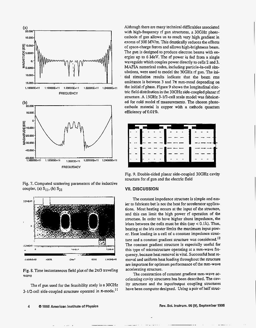
The matching can be made by using either reactive irises or reactive stubs: the irises and the stubs can be ei- ther inductive or capacitive. The inductive irises have an indentation somewhere between the top and the bottom surfaces of the half structure, and the capacitive irises can have full height with smaller gap in between. A case with inductive irises has been computer-simulated using MAFIA codes. Figure 6 shows the inductive inputlout- put coupler design used for the planar cavity structure. The scattering parameters, S I I and S21. of a seven-cell structure are shown in Figure 7. A time instantaneous electric field plot of the 2rd3 traveling wave is shown in Figure 8,
the shunt impedance (s > 0.lmm) becomes lower at greater cutwidths.
0 . m . ‘ ’ I . .
-
s 0 . m -
0.0302 -
0.W 0.02 OM 0.m 0.W : (m)
Fig. 5. Cutwidth s of a 120GHz structure along z-axis.
V. INPUT/OUTPUT COUPLERS
The accelerating structures must be fed by an exter- nal rf power source. The cavity structure is fed through a rectangular waveguide which is a natural choice for a DXL-processed planar structure. The rectangular waveguide connects to the coupling cell, which requires impedance matched to the periodic structure. The imped-
Rev. Sci. Instrum. 66 (9), September 1995
Fig. 6. Bottom half of inputloutput couplers used in the simulation for a planar cavity structure.
VI. RF GUN STRUCTURE
The next generation of linear collider and short wavelength free-electron lasers imposes stringent re- quirements on the quality of the electron beam. The rf photocathode source pla)s 3 key role in obtaining small emittance beams with ultra-high brightness suitable for these applications. At the PXC95 conference, MIT re- searchers working on a 15GHz rf photocathode gun re- ported encouraging results using high frequency rf gun structures for generation of low emittance and high brightness beams. At Argonne. we have started a feasi- bility study for a 30GHz rf photocathode source based on a double-sided planar DXL structure. Recent results on DXL exposures presented by Guckel‘s group at the Uni- versity of Wisconsin indicate that I-cm-deep x-ray expo sure is possible.
@ 1995 American Institute of Physics 3
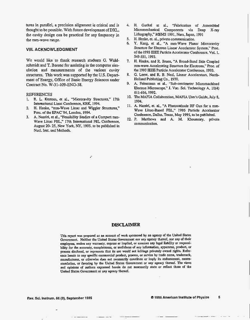
Although there are many technical difficulties associated with high-frequency rf gun structures, a 30GHz photo- cathode rf gun allows us to reach very high gradient in excess of 500 lMV/m. This drastically reduces the effects of space-charge forces and allows high-brightness beam. The gun is designed to produce electron beams with en- ergies up to 6 MeV. The rf power is fed from a single waveguide which couples power directly to cells 2 and 3. MAFIA numerical codes, including particle-in-cell sim- ulations, were used to model the 30GHt rf gun. The ini-
‘ tial simulation results indicate that the beam rms emittance is between 3 and 75c mm-mrad depending on
1.16MH)E+11 1,18000E+11 1,2m-+11 l,zoooE+ll 1.24000E+11 the initial rf phase. Figure 9 shows the longitudinal elec- tric field distribution in the 30GHz side-coupled planar rf structure. A 15GHz 3-1/2-cell scale model was fabricat- ed for cold model rf measurements. The chosen photo- cathode material is copper with a cathode quantum efficiency of 0.01%.
FREQUENCY
-5o.Ooo ’ I l.lMXX)E+ll 1.18000€+11 1 , 2 0 0 ~ ~ ~ 1 1 1.220WFll 1.24OooE+11
FREQUENCY
Fig. 9. Double-sided planar side-coupled 30GHz cavity structure for rf gun and the electric field
VII. DISCUSSION Fig. 7. Computed scattering parameters of the inductive coupler, (a) SI I , (b) S21
Fig. 8. Time instantaneous field plot of the 2 d 3 traveling wave
The rf gun used for the feasibility study is a 30GHz 3- I/Zcell side-coupled structure operated in E-mode.’ ’
The constant impedance structure is simple and eas- ier to fabricate but is not the best for accelerator applica- tions. Most heating occurs at the input of the structure, and this can limit the high power rf operation of the structure. In order to have higher shunt impedance, the irises between the cells must be thin (say c 0. I A). Thus, heating at the ins center limits the maximum input pow- er. Heat loading in a cell of a constant impedance svuc- ture and a constant gradient structure was considered.” The constant gradient structure is especially useful for this type of microstructure operating at a mm-wave fre- quency, because heat removal is vital. Successful heat re- moval and uniform heat loading throughout the structure are important for optimum performance of the mm-wave acceleratin, CI structure.
The construction of constant gradient mm-wave ac- celerating cavity structures has been described. The cav- ity structure and the inpudoutput coupling structures have been computer designed. Using a pair of half struc-
4 @I 1995 American Institute of Physics Rev. Sci. Instrum. 66 (9). September 1995
tures in parallel, a precision alignment is critical and is thought to be possible. With future development of DXL, the cavity design can be practical for any frequency in the mm-wave range.
VIII. ACKNOWLEDGMENT
We would like to thank research students G. Wald- Schmidt and T. Berenc for assisting in the computer sim- ulation and measurements of the various cavity structures. This work was supported by the U.S. Depart- ment of Energy, Ofice of Basic Energy Sciences under Con tract No. W-3 1 - 109-ENG-3 8.
REFERENCES 1.
2.
3.
R. L. Kustom, et al., “Microcavity Structures,” 17th International Linac Conference, KEK, 1994. H. Henke, “mm-Wave Linac and Wiggler Structures,” Proc. of the EPAC ’94, London, 1994. A. Nassiri, et al., “Feasibility Studies of a Compact mm- Wave Linac EL,” 17th International FEL Conference, August 20- 25, New York. NY, 1995, to be published in Nucl. Inst. and Methods.
4.
5. 6.
7.
8.
9.
H. Guckel at al.. “Fabrication of Assembled Micromechanical Components via Deep X-ray Lithography,” IMEMS 1991. Nara, Japan, 1991 H. Henke. et. al.. private communication. Y. Kang, et al., “A mm-Wave Planar Microcavity Structure for Electron Linear Accelerator System.” Proc. of the 1993 IEEE Particle Accelerator Conference, Vol. 1.
H. Henke, and R. Bruns. “A Broad-Band Side Coupled mm-wave Accelerating Structure for Electrons.” Roc. of the 1993 IEEE Particle Accelerator Conference. 1993. G. Loew, and R. B. Neal. Linear Accelerators, North- Holland Publishing Co.. 1970. A. Feinerman et al., “Sub-centimeter Micromachined Electron Microscope,” J. Vac. Sci. Technology A. lO(4)
549-551, 1993.
61 1-616,1992. 10. The MAFIA Collaboration, MAFIA User‘s Guide, July 8.
1994. 11. A. Nassiri. et. al.. “A Photocathode RF Gun for a mm-
Wave Linac-Based FEL,” 1995 Particle Accelerator Conference, Dallas. Texas, May 1995, to be published.
12. P. Matthews and A. M. Khounsary. private communication.
I’
DISCLAIMER
This report was prepared as an account of work sponsored by an agency of the United States Government. Neither the United States Government nor any agency thereof, nor any of their employees, makes any warranty, express or implied, or assumes any legal liability or responsi- bility for the accuracy, completeness, or usefulness of any information, apparatus, product, or process disclosed, or represents that its use would not infringe privately owned rights. Refer- ence herein to any specific commercial product, process, or service by trade name, trademark, manufacturer, or otherwise does not necessarily constitute or imply its endorsement, recom- mendation, or favoring by the United States Government or any agency thereof. The views and opinions of authors expressed herein do not necessarily state or reflect those of the United States Government or any agency thereof.
Rev. Sci. Instrum. 66 (9), September 1995 Q 1995 Amw-can Institute of Physics 5


![Cavity Field Control · Vector Sum Control of Pulsed Accelerating Fields in Lorentz Force Detuned Superconducting Cavities. Ph. D. Thesis of DESY, 1998 [3] M. Hoffmann. Development](https://img.pdfslide.us/doc/110x75/5fb38ceca806c2129b20c3b4/cavity-field-control-vector-sum-control-of-pulsed-accelerating-fields-in-lorentz.jpg)