Embed Size (px)
Citation preview

1
Design and Characterization of Submicron CCDs in CMOS
Keith Fife, Abbas El Gamal, Philip WongDepartment of Electrical Engineering, Stanford University, Stanford, CA 94305
2009 International Image Sensor Workshop

2
Camera History
• Despite progress, each of these cameras form images in the same way

3
Image Formation in a Camera
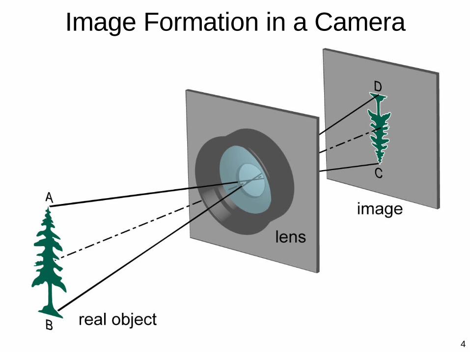
4
Image Formation in a Camera

5
Image Formation in a Camera
6
Outline
• Multi-Aperture application
• FT-CCD array– Surface-channel
– Buried-channel– Pinned phase buried-channel
• Results
• Summary
7
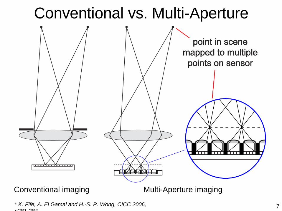
Conventional vs. Multi-Aperture
Conventional imaging Multi-Aperture imaging
* K. Fife, A. El Gamal and H.-S. P. Wong, CICC 2006, p281-284
8
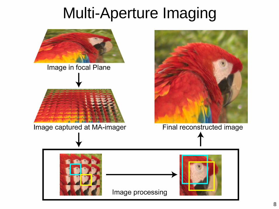
Multi-Aperture Imaging
9
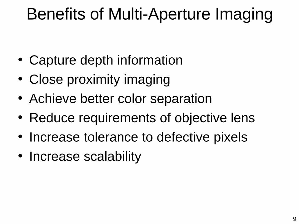
Benefits of Multi-Aperture Imaging
• Capture depth information
• Close proximity imaging
• Achieve better color separation• Reduce requirements of objective lens
• Increase tolerance to defective pixels
• Increase scalability
10
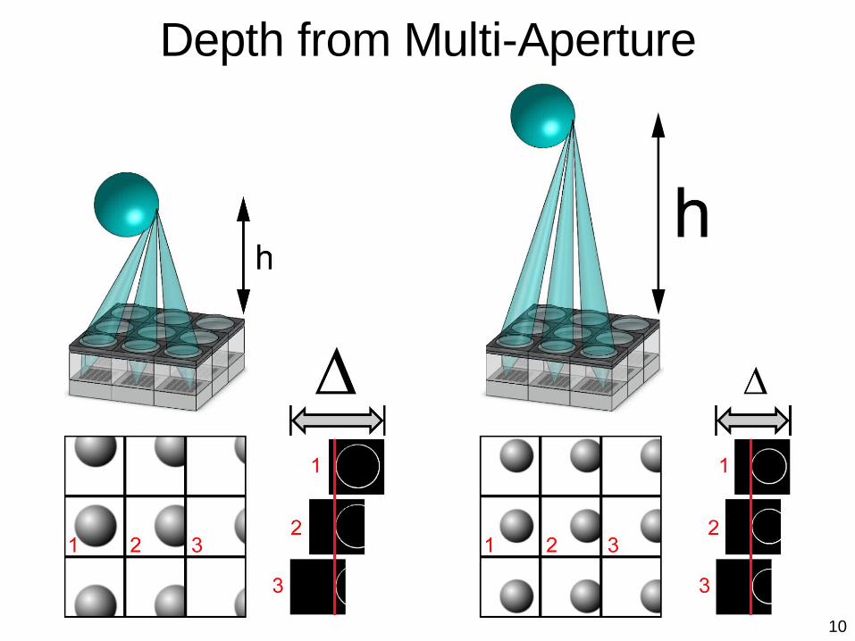
Depth from Multi-Aperture
11
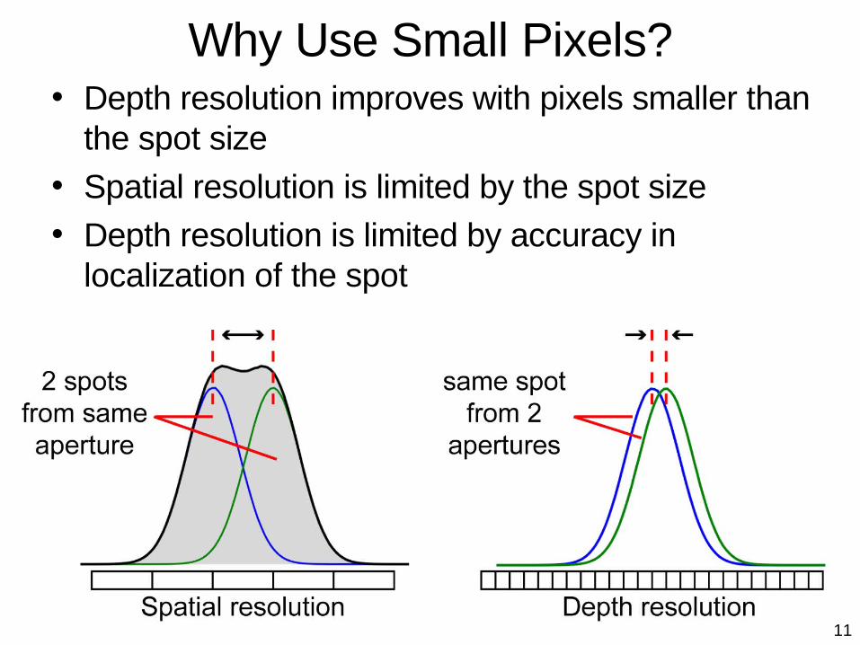
Why Use Small Pixels?• Depth resolution improves with pixels smaller than
the spot size• Spatial resolution is limited by the spot size• Depth resolution is limited by accuracy in
localization of the spot

12
Feature Localization vs. Pixel Size
Poor location accuracy High location accuracy
Pixels
13
Implementation
• Submicron pixels are difficult to build
• Small, disjoint arrays of pixels (clusters) are needed for MA architecture– Easier to implement pixels as clusters
– Several performance advantages
• We selected a hybrid CCD/CMOS image sensor architecture

14
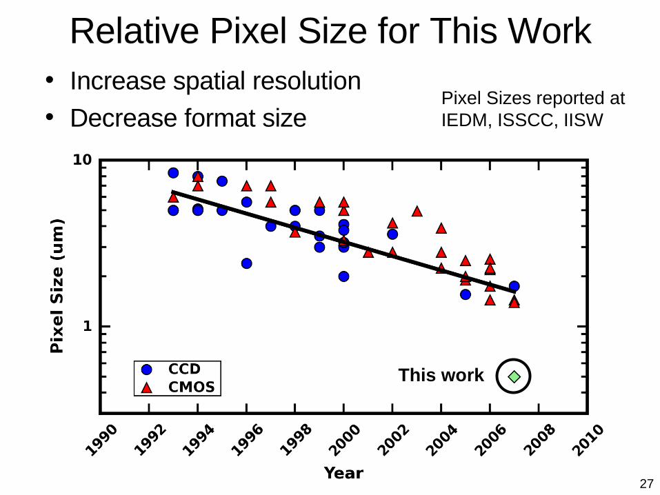
• Increase spatial resolution• Decrease format size
Pixel Sizes reported at IEDM, ISSCC, IISW
Recent Pixel Scaling
15
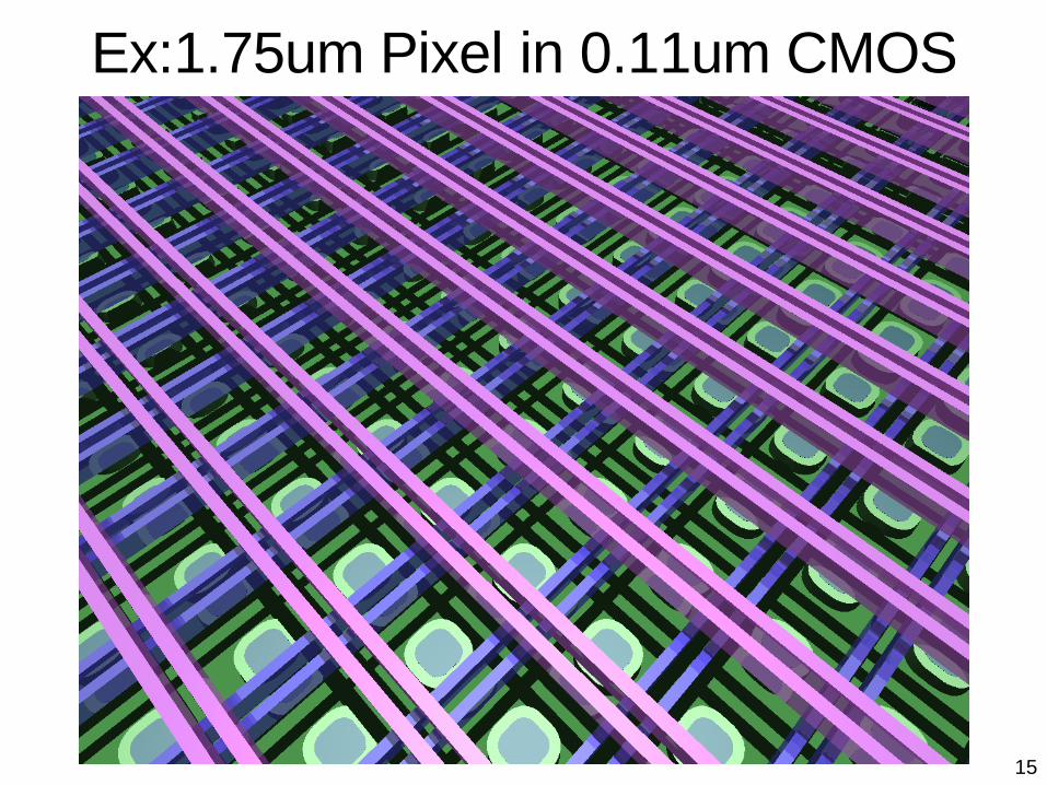
Ex:1.75um Pixel in 0.11um CMOS
16
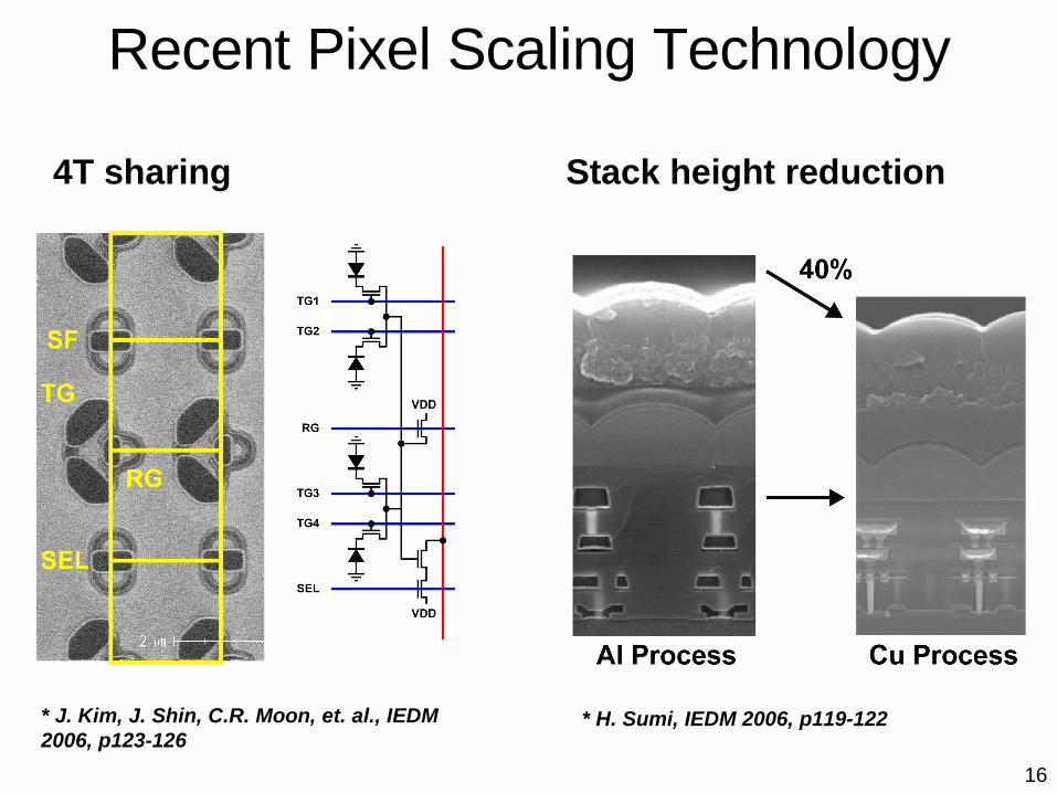
Recent Pixel Scaling Technology
* H. Sumi, IEDM 2006, p119-122* J. Kim, J. Shin, C.R. Moon, et. al., IEDM 2006, p123-126
4T sharing Stack height reduction
17
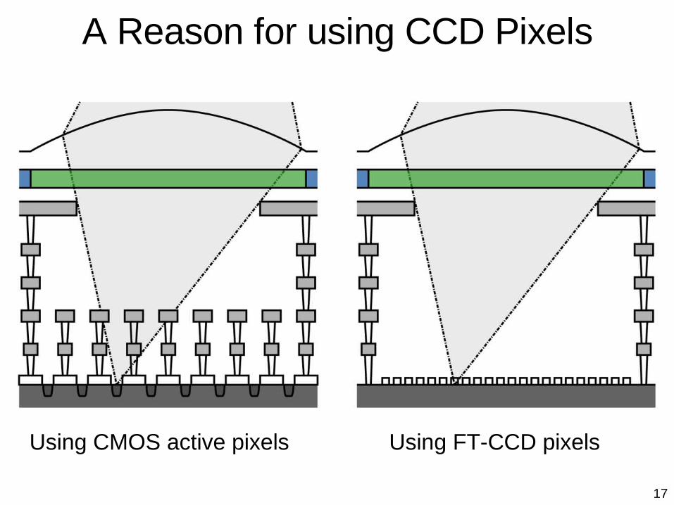
A Reason for using CCD Pixels
Using CMOS active pixels Using FT-CCD pixels
18
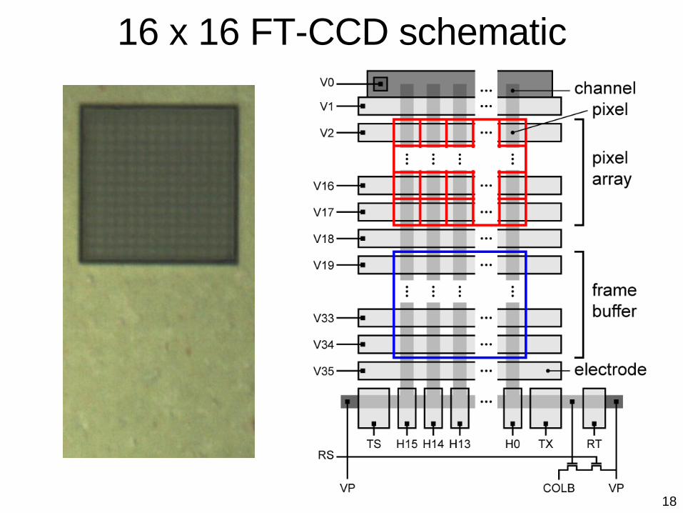
16 x 16 FT-CCD schematic
19
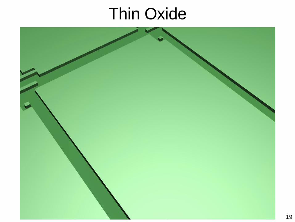
Thin Oxide
20
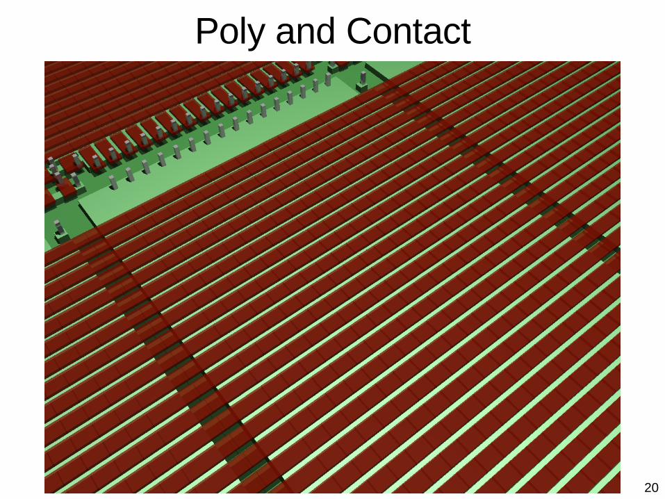
Poly and Contact
21
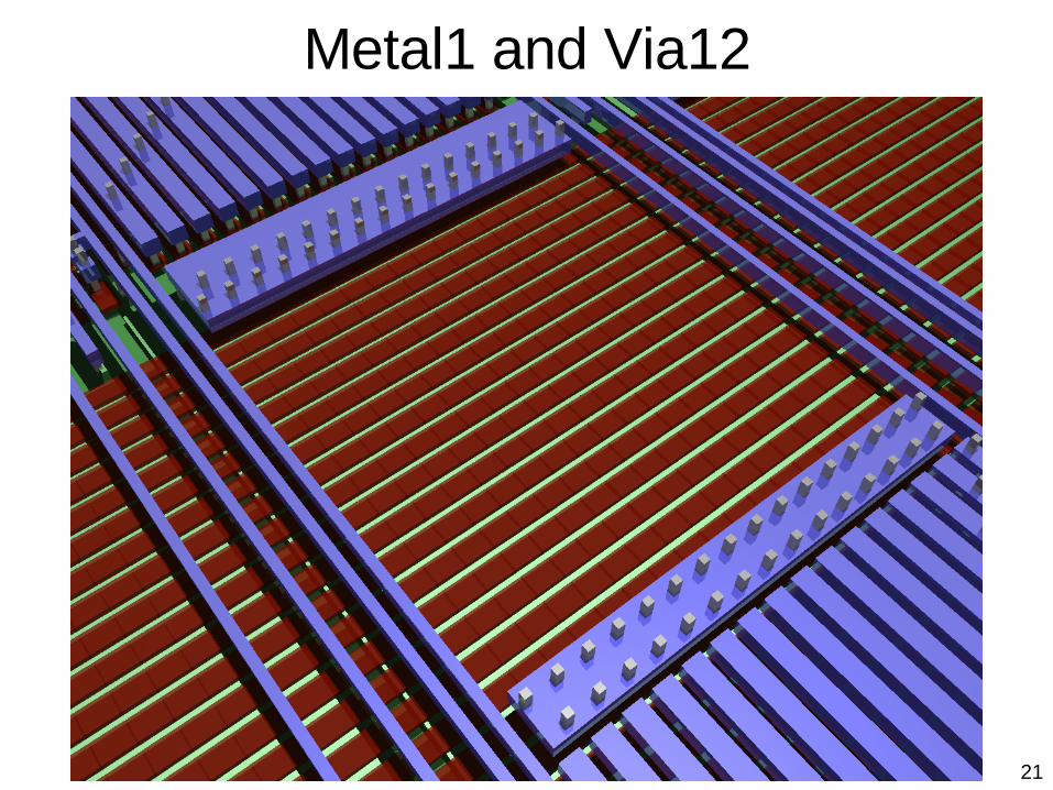
Metal1 and Via12
22
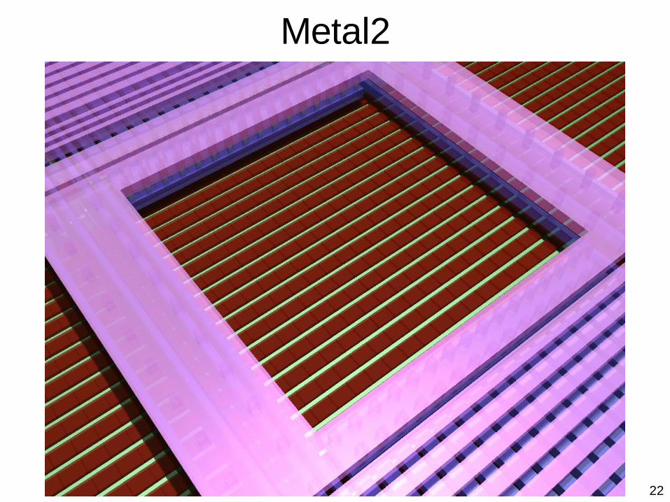
Metal2
23
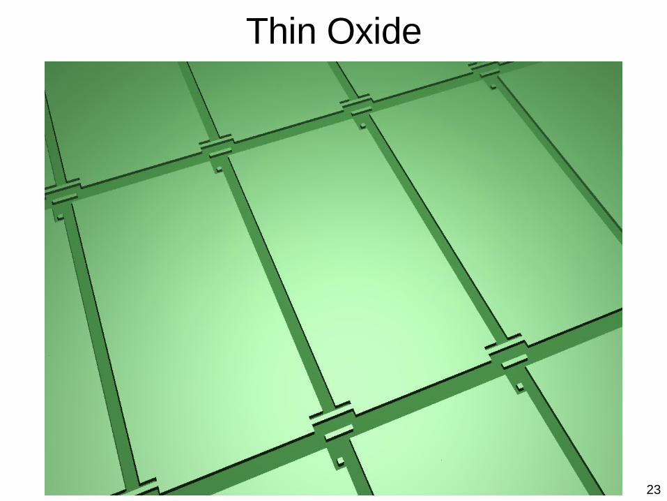
Thin Oxide
24
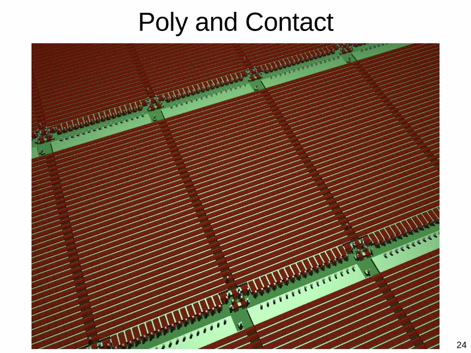
Poly and Contact
25
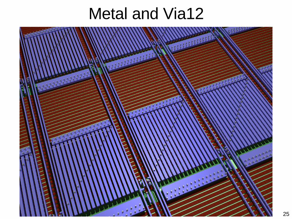
Metal and Via12

26
Metal2
27
• Increase spatial resolution• Decrease format size
This work
Pixel Sizes reported at IEDM, ISSCC, IISW
Relative Pixel Size for This Work
28
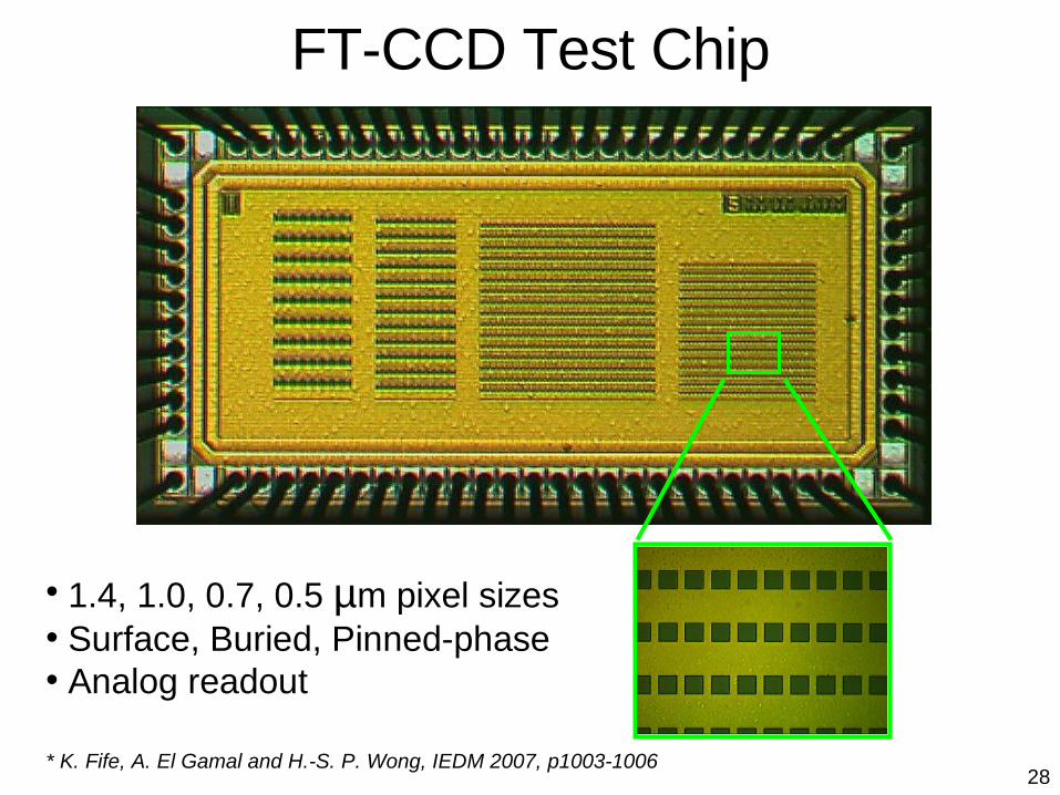
FT-CCD Test Chip
* K. Fife, A. El Gamal and H.-S. P. Wong, IEDM 2007, p1003-1006
• 1.4, 1.0, 0.7, 0.5 µm pixel sizes• Surface, Buried, Pinned-phase• Analog readout
29
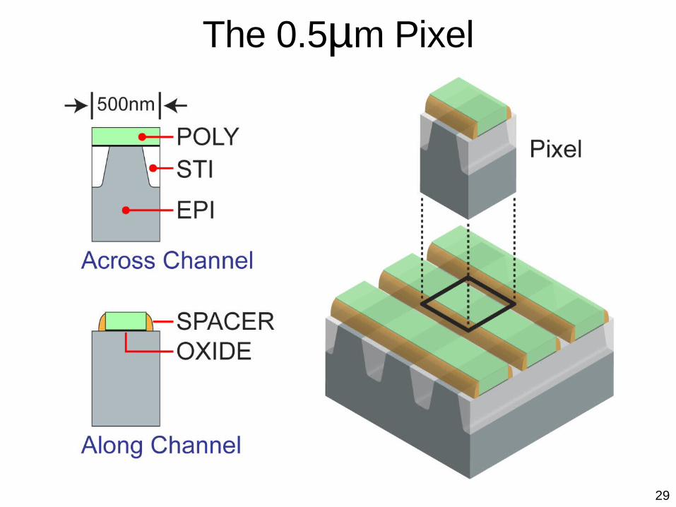
The 0.5µm Pixel
30
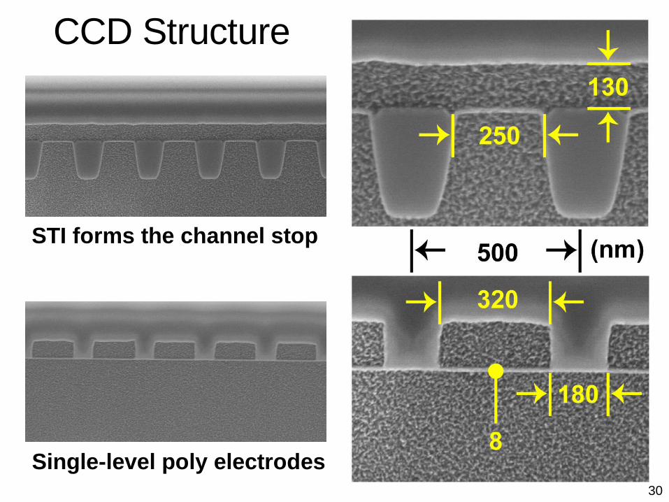
CCD Structure
STI forms the channel stop
Single-level poly electrodes

31
The 0.7µm Buried Channel Pixel
33
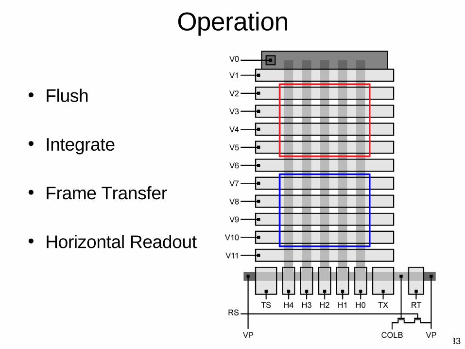
• Flush
• Integrate
• Frame Transfer
• Horizontal Readout
Operation

34
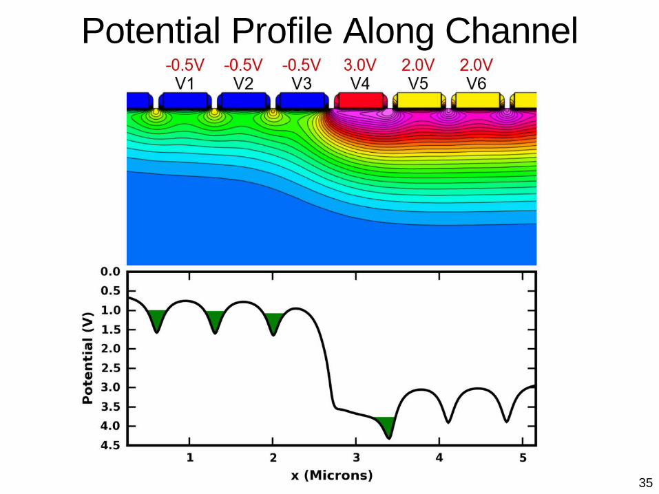
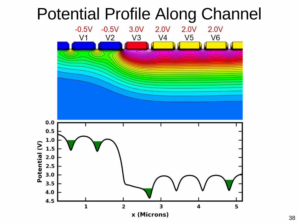
Potential Profile Along Channel
35
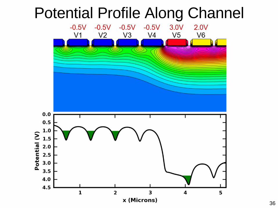
Potential Profile Along Channel
36
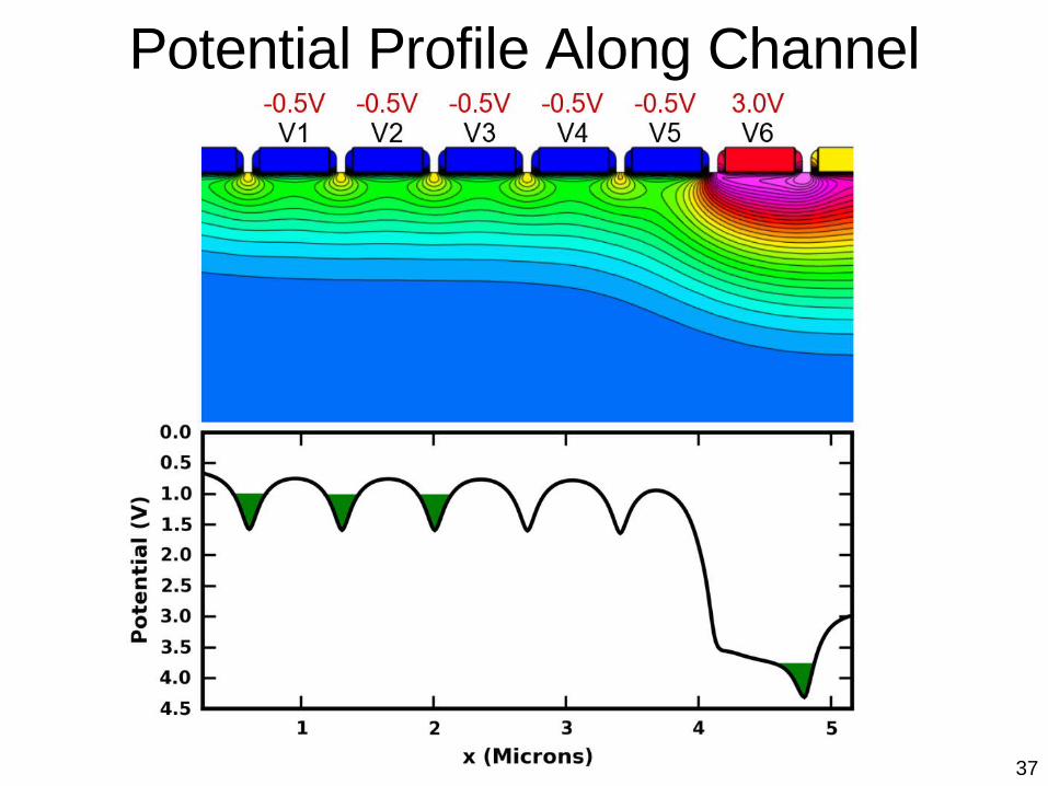
Potential Profile Along Channel
37
Potential Profile Along Channel
38
Potential Profile Along Channel
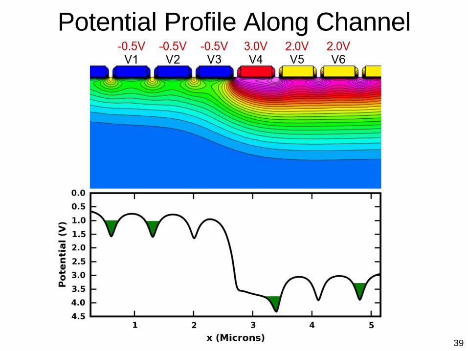
39
Potential Profile Along Channel

40
Potential Profile Along Channel
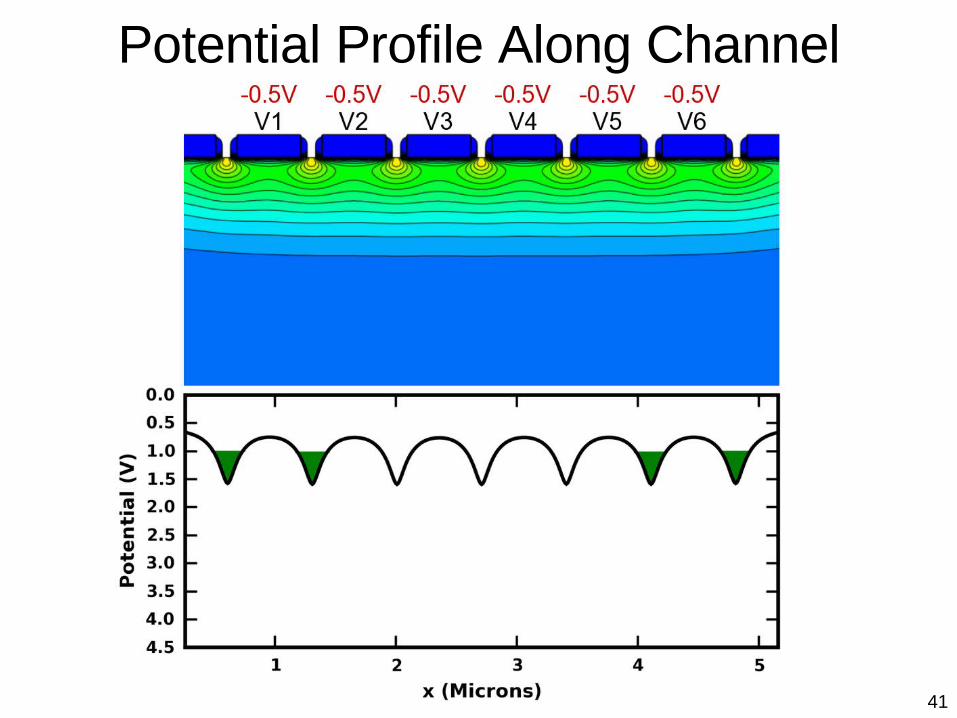
41
Potential Profile Along Channel
42
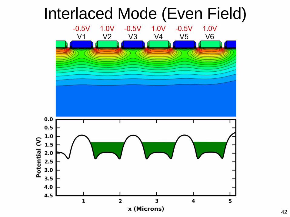
Interlaced Mode (Even Field)
43
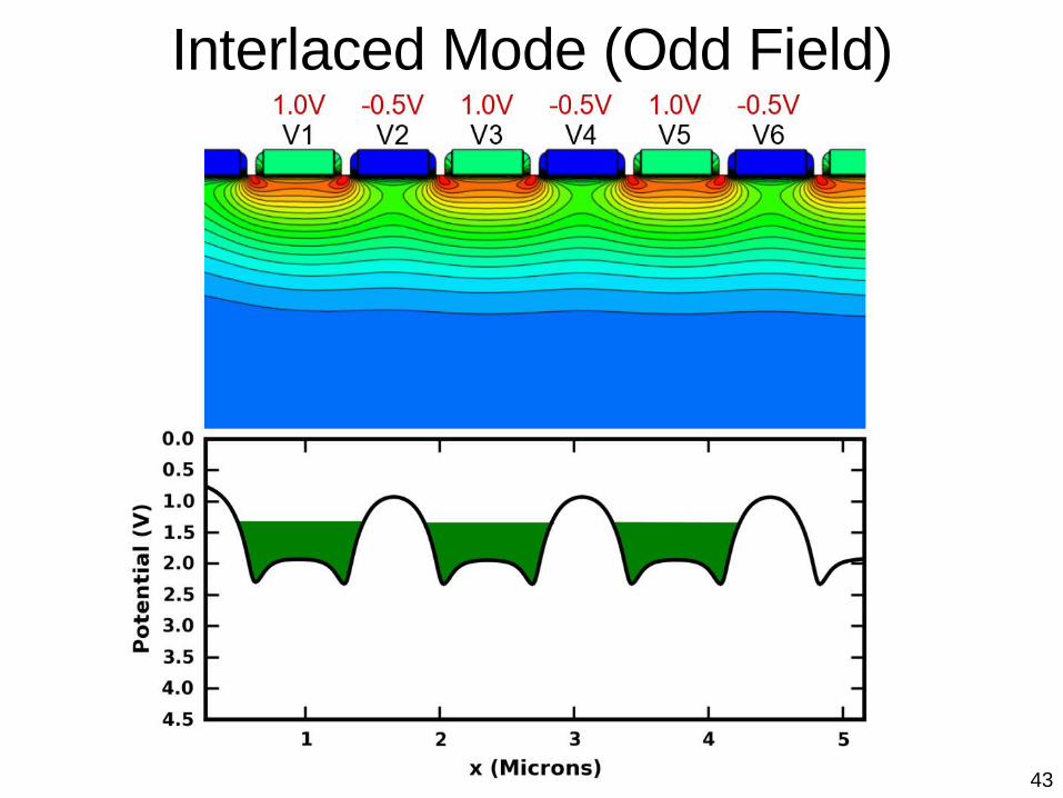
Interlaced Mode (Odd Field)
44
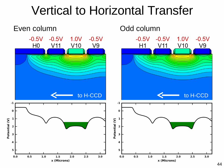
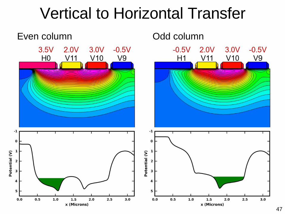
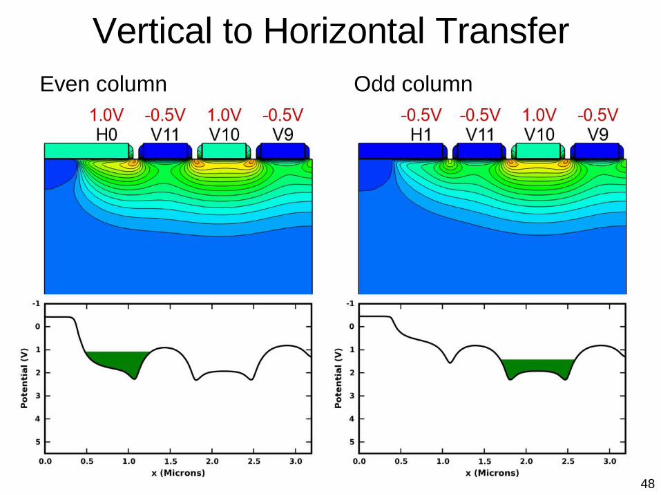
Even column Odd column
Vertical to Horizontal Transfer
to H-CCD to H-CCD
45
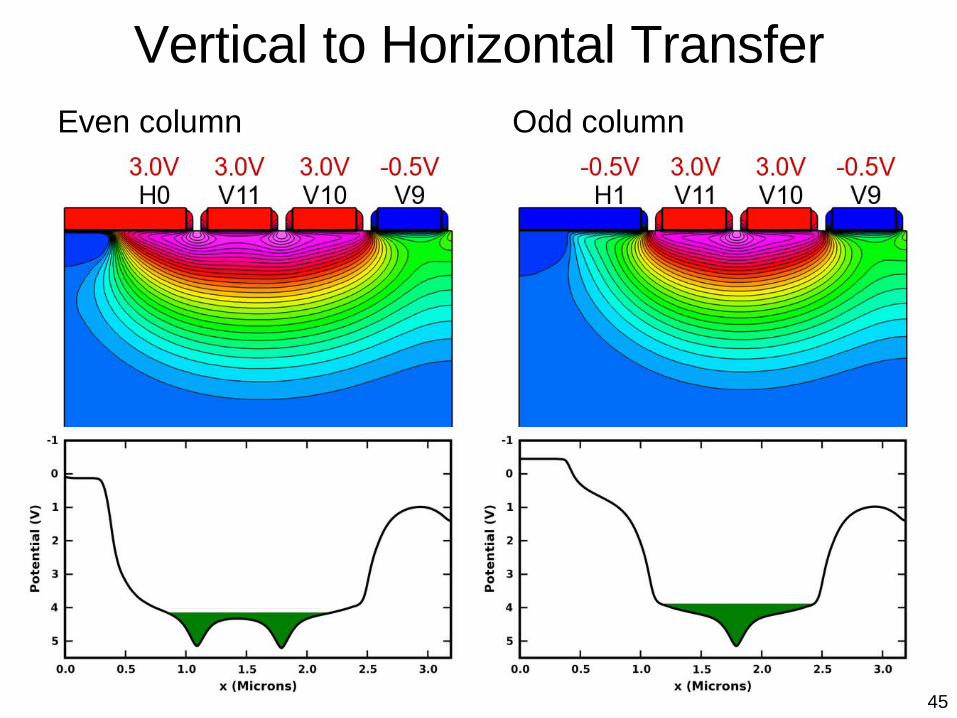
Even column Odd column
Vertical to Horizontal Transfer
46
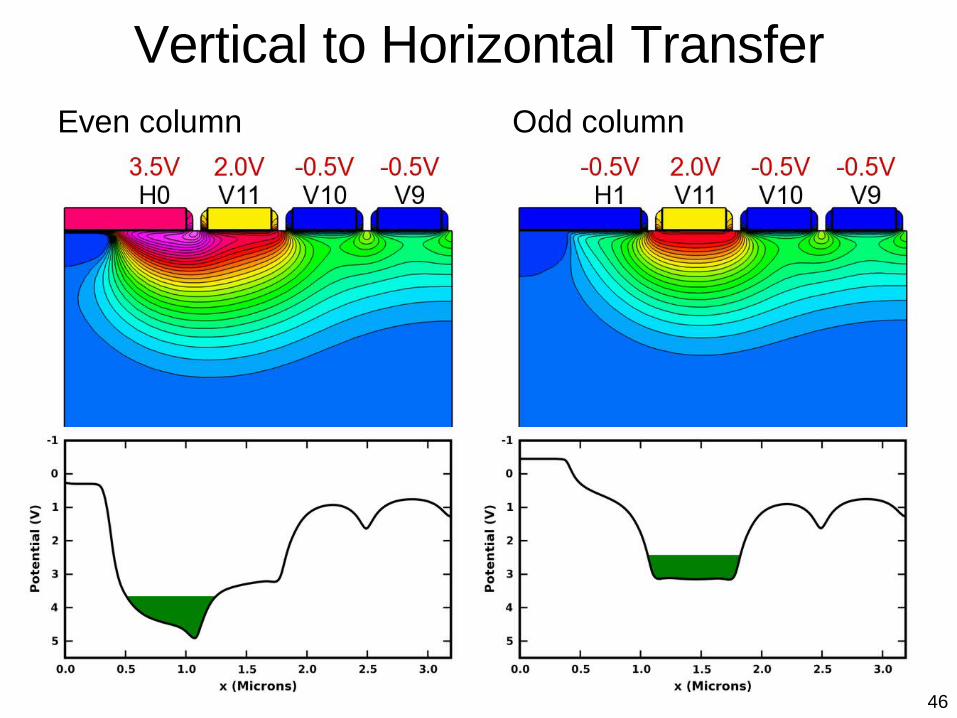
Even column Odd column
Vertical to Horizontal Transfer
47
Even column Odd column
Vertical to Horizontal Transfer
48
Even column Odd column
Vertical to Horizontal Transfer
49
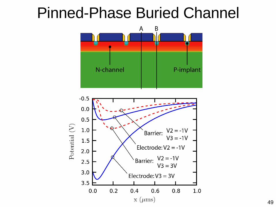
Pinned-Phase Buried Channel
50
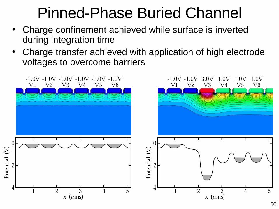
Pinned-Phase Buried Channel• Charge confinement achieved while surface is inverted
during integration time• Charge transfer achieved with application of high electrode
voltages to overcome barriers
51
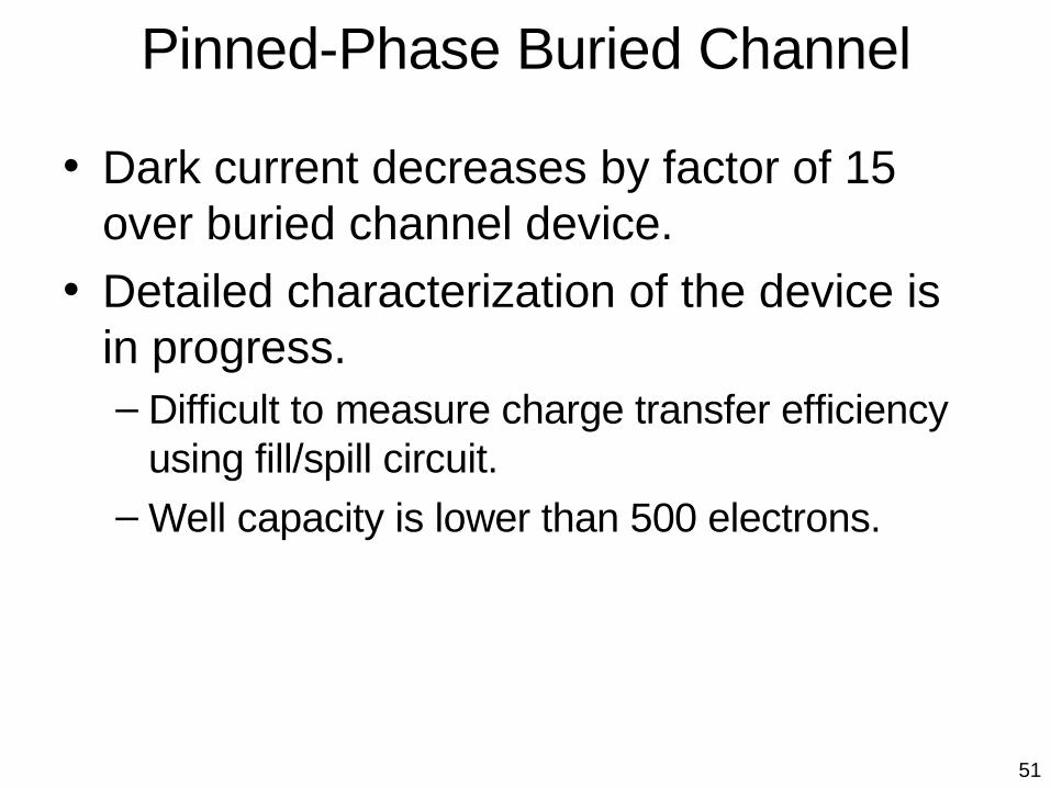
Pinned-Phase Buried Channel
• Dark current decreases by factor of 15 over buried channel device.
• Detailed characterization of the device is in progress.– Difficult to measure charge transfer efficiency
using fill/spill circuit.– Well capacity is lower than 500 electrons.
52
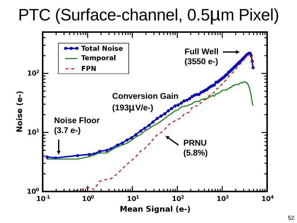
Noise Floor(3.7 e-)
Full Well(3550 e-)
PRNU(5.8%)
Conversion Gain
(193µV/e-)
PTC (Surface-channel, 0.5µm Pixel)

53
Noise Floor(5 e-)
Full Well(3500 e-)
PRNU(2%)
Conversion Gain
(165µV/e-)
PTC (Buried-channel, 0.7µm Pixel)
54
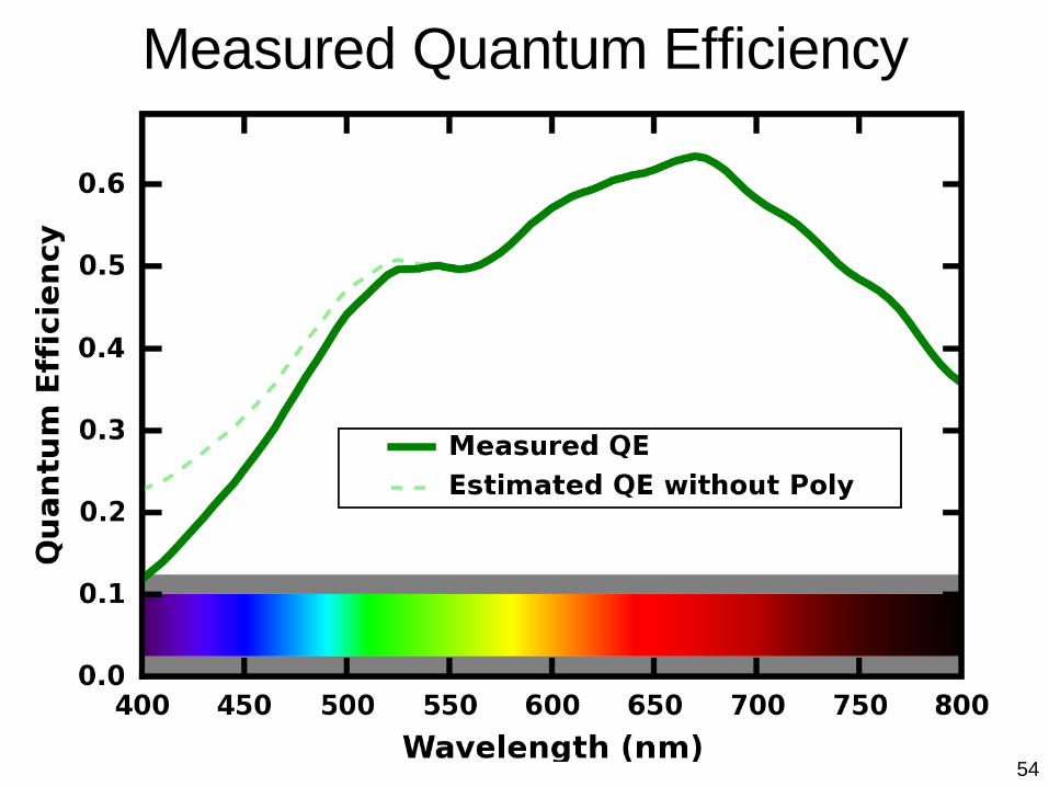
Measured Quantum Efficiency
55
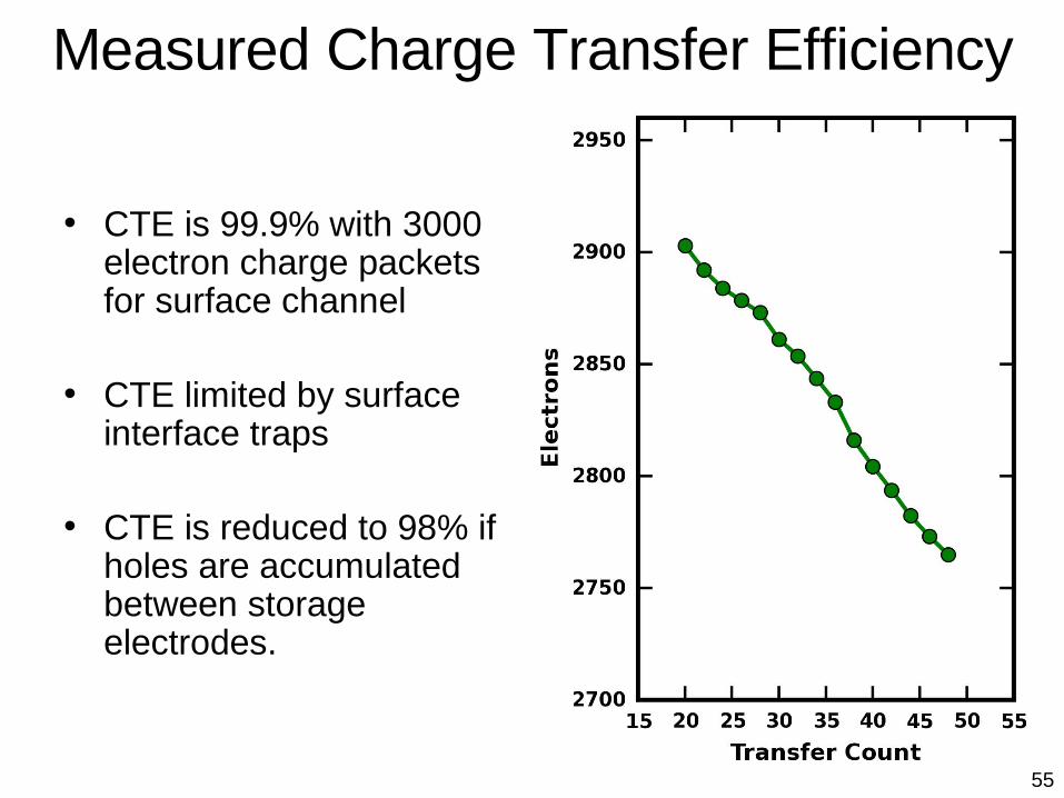
• CTE is 99.9% with 3000 electron charge packets for surface channel
• CTE limited by surface interface traps
• CTE is reduced to 98% if holes are accumulated between storage electrodes.
Measured Charge Transfer Efficiency
56
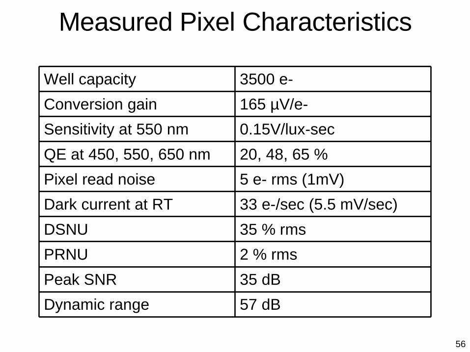
Measured Pixel Characteristics
57 dBDynamic range
35 dBPeak SNR
2 % rmsPRNU
35 % rmsDSNU
33 e-/sec (5.5 mV/sec)Dark current at RT
5 e- rms (1mV)Pixel read noise
20, 48, 65 %QE at 450, 550, 650 nm
0.15V/lux-secSensitivity at 550 nm
165 µV/e-Conversion gain
3500 e-Well capacity

57
Images from Single Subarray
Captured with F/2.8, f=6mm lens at 1/10 sec
Raw data Added contrast
Electrical Optical Optical
3000 electron charge packets from fill/spill input
58
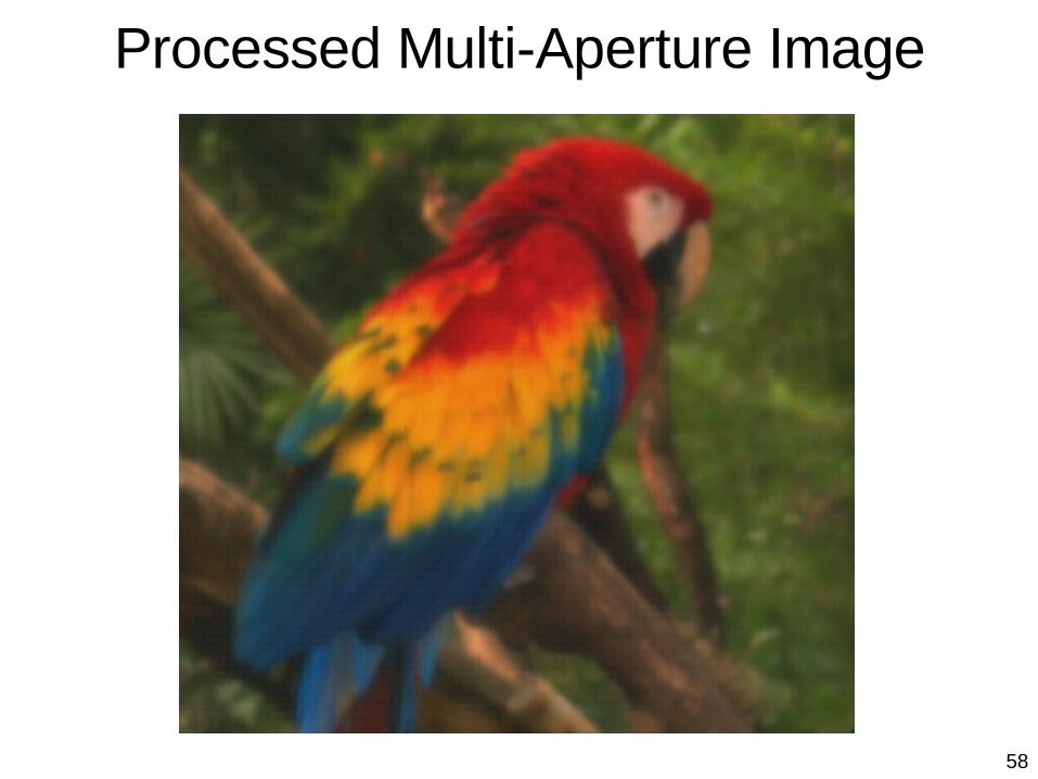
Processed Multi-Aperture Image
59
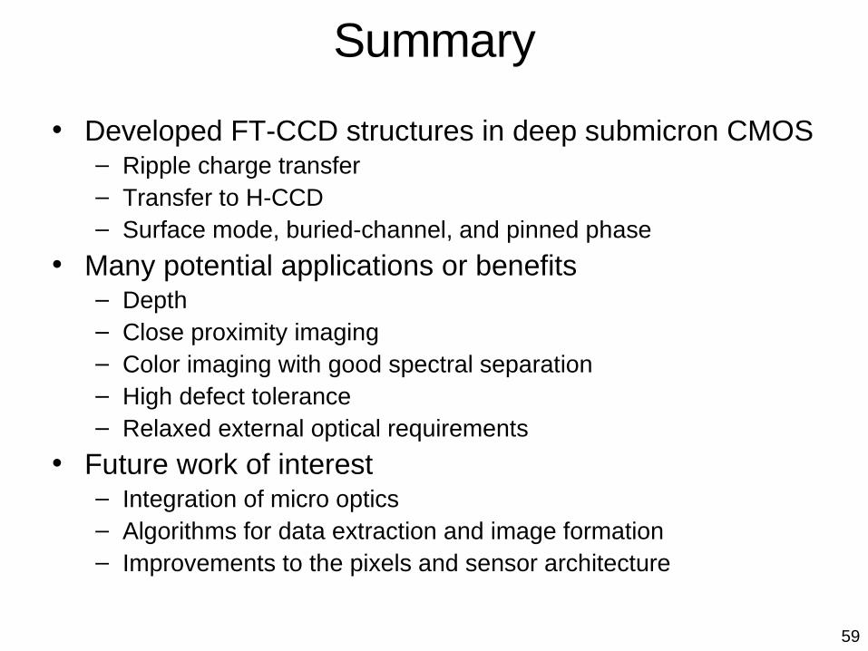
Summary
• Developed FT-CCD structures in deep submicron CMOS– Ripple charge transfer– Transfer to H-CCD– Surface mode, buried-channel, and pinned phase
• Many potential applications or benefits– Depth– Close proximity imaging– Color imaging with good spectral separation– High defect tolerance– Relaxed external optical requirements
• Future work of interest– Integration of micro optics– Algorithms for data extraction and image formation– Improvements to the pixels and sensor architecture
60
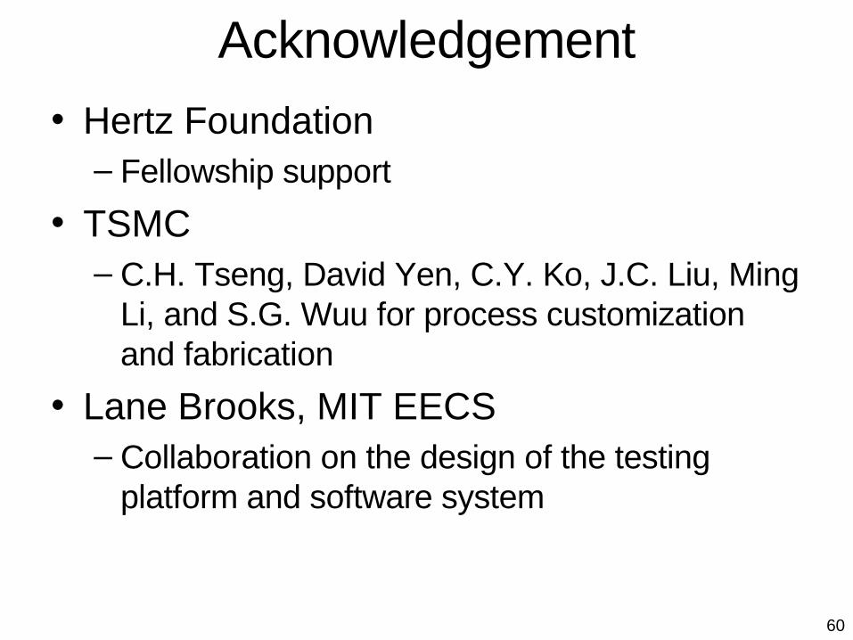
Acknowledgement
• Hertz Foundation– Fellowship support
• TSMC– C.H. Tseng, David Yen, C.Y. Ko, J.C. Liu, Ming
Li, and S.G. Wuu for process customization and fabrication
• Lane Brooks, MIT EECS– Collaboration on the design of the testing
platform and software system