Embed Size (px)
Citation preview

Design And Characterization Of Multi-Layer Coplanar Waveguid Baluns And Inductors
by
Khaled Obeidat
A thesis submitted in partial fulfillment of the requirements for the degree of
Master of Electrical Engineering Department of Electrical Engineering
College of Engineering University of South Florida
Major Professor: Tom M. Weller, Ph.D. Lawrance P. Dunleavy, Ph.D Horace C. Gordon, Jr., M.S.E
Date of Approval: July 1, 2003
Keywords: model, marchand,antenna, compensation, spiral
© Copyright 2003 , Khaled Ahmad Obeidat

DEDICATION
To my mother Haia, my brother Omar, my sisters Rash and Loda, my wife Noor, and
in memory of my father Ahmad Obeidat, who had been through a lot.

ACKNOWLEDGEMENTS
I sincerely thank my advisor, Dr. Tom Weller, for his guidance throughout the
program and for his unlimited support. His professional insight added considerably to
my graduate education. It was comforting to find his door always open to discuss my
problems and concerns. I would like also to thank my committee members for
reviewing my thesis and participating in my defense.
My deepest thanks go to the faculty and staff members of the WAMI
Laboratory, and in particular to Professors Lawrance Dunleavy and Horace Gordon.
Also I thanks my colleagues who contributed to this work through many interesting
disucssions: Eid Alsabbagh, Clemente Toro, Lester Lopez, Christopher Trent, Balaji
Lakshminarayanan, Sathya Padmanabhan, Mark Laps, Thomas Ketterl, Catherine
Boosales, Hariharasudhan Kannan , Saravana Natarajan and Alberto Rodriguez.
I would like to thank my advisor in my undergrad study, Dr. Nihad Dib who
was always there to support me with his valube advices and for his help that led me to
continue my higher education in the United Sates.
Finaly I thank my family for their patient and support, most importantly my
mother Haia and my wife Noor who never failled to believe in me.

i
TABLE OF CONTENTS
LIST OF TABLES............................................................................................................. iii
LIST OF FIGURES ........................................................................................................... iv
ABSTRACT...................................................................................................................... xii
CHAPTER 1 – INTRODUCTION ..................................................................................... 1
1.1 Introduction....................................................................................................... 1 1.2 Thesis Organization .......................................................................................... 3 1.3 Research Contributions..................................................................................... 4
CHAPTER 2 - BALUN BACKGROUND......................................................................... 5
2.1 Introduction....................................................................................................... 5 2.2 Marchand Balun................................................................................................ 7 2.3 Monolithic Planar Marchand Balun................................................................ 11 2.4 Enhanced Marchand Balun............................................................................. 13
2.4.1 Compensated Coupled Lines ................................................................... 13 2.4.2 Short Transmission Line Between the Couplers...................................... 14
2.5 Parallel Connected Marchand Balun .............................................................. 16 2.6 Multilayer Spiral Transmission-Line Balun ................................................... 17 Summary............................................................................................................... 20
CHAPTER 3 – DESIGN AND ANALYSES OF A MULTILAYER CPW SPIRAL BALUN............................................................................................................................. 21
3.1 Introduction..................................................................................................... 21 3.2 Design Procedure of the Multilayer CPW Spiral Balun ................................. 23 3.3 Compensation Techniques.............................................................................. 25
3.3.1 Ground plane below the air bridge and between the two couplers .......... 25 3.3.1.1 Changing the Ground Width and Air Bridge Width......................... 27 3.3.1.2 Changing air bridge height................................................................ 32 3.3.1.3 Insulator permittivity ........................................................................ 34
3.3.2 The Capacitance between the air bridge and the spiral............................ 38 3.3.3 Open circuit capacitance .......................................................................... 40
3.4 Design Specification ....................................................................................... 43 Summary............................................................................................................... 45
CHAPTER 4 – EQUIVALENT MULTILAYER CPW SPIRAL BALUN MODEL ...... 47
4.1 Introduction..................................................................................................... 47

ii
4.2 Equivalent Split model for the Multilayer spiral Balun.................................. 48 4.3 Equivalent Lumped Elements Model for the Multilayer Spiral Balun........... 58 Summary............................................................................................................... 69
CHAPTER 5 – MEASUREMENT RESULTS ................................................................ 70
5.1 Introduction..................................................................................................... 70 5.2 Balun number 1............................................................................................... 71 5.3 Balun number 2............................................................................................... 80 5.4 Balun number 3............................................................................................... 88 5.5 Balun number 4............................................................................................... 97 5.6 Balun Performance. ...................................................................................... 105 Summary............................................................................................................. 107
CHAPTER 6 – COMPARISON OF MoM AND FDTD................................................ 108
6.1 Introduction................................................................................................... 108 6.2 Finite-Difference Time-Domain method (FDTD)........................................ 109 6.3 Method of Moments...................................................................................... 110 6.4 Discussion of the results ............................................................................... 110 Summary............................................................................................................. 117
CHAPTER 7 – THE EFFECT OF THE GROUND PLANE ON THE SPIRAL INDUCTOR MODEL..................................................................................................... 118
7.1 Introduction................................................................................................... 118 7.2 Spiral Inductor .............................................................................................. 127 7.3 Lumped Element Model ............................................................................... 132 Summary............................................................................................................. 137
CHAPTER 8 – CONCLUSIONS AND RECOMMENDATIONS................................ 138
8.1 Conclusion .................................................................................................... 138 8.2 Recommendations......................................................................................... 139
REFERENCES ............................................................................................................... 140
APPENDICES ................................................................................................................ 143
APPENDIX A - BALUN GEOMETRICAL DIMENSIONS ............................ 144 APPENDIX B – FOUR-PORT ON-WAFER TRL CALIBRATION AND BALUN MEASUREMENT PROCEDURE....................................................... 149 B.1 Equipments Configuration ........................................................................... 149 B.2 Calibration Kit.............................................................................................. 150 B.3 Calibration Setup.......................................................................................... 150 B.4 Calibration Measurement ............................................................................. 152 B.5 Calculating Correction Factor ...................................................................... 160 B.6 Making The Four-Port Measurement........................................................... 161 B.6 De-embedding The Four-Port Measurement ............................................... 161 B.7 Display corrected Four-Port Data ................................................................ 162

iii
LIST OF TABLES
Table 3. 1 - Design parameters of the small and large size baluns, see Figure 3.22 –
Figure 3.24 for visualization. ........................................................................ 43 Table 4. 1 - The optimized parameter values of the equivalent model............................. 62 Table 5. 1 - Comparison between the previously reported balun performance results
and our balun design results (the small and the large size baluns). ............ 106 Table 6. 1 - Cells description for the balun (balun #1 in Appendix A) structure
simulated using Empire............................................................................... 110 Table A. 1 - Common geometrical dimension of the small size balun.See (Figure
3.22 – Figure 3.24) in section 3.4 for parameters visualization................. 144

iv
LIST OF FIGURES
Figure 1. 1 - Simple dipole with balanced feed. ................................................................. 2 Figure 1. 2 - Radiation diagram of a dipole with balun in free space................................. 2 Figure 1. 3 - Radiation diagram of a dipole without balun................................................. 2 Figure 2. 1 - Balanced two wire transmission line, |I1| = |I2|............................................... 5 Figure 2. 2 - Unbalanced transmission lines (a) coaxial cable and (b) microstrip.............. 6 Figure 2. 3 - Coaxial Cross section of compensated Marchand balun................................ 7 Figure 2. 4 - Wide band coaxial Marchand balun............................................................... 8 Figure 2. 5 - Equivalent circuit diagram of the wide band coaxial Marchand balun.......... 9 Figure 2. 6 - Monolithic planar Marchand balun.............................................................. 11 Figure 2. 7 - The bottom two strip lines serve as a short-circuit stub............................... 12 Figure 2. 8 - Capacitive-compensated Marchand balun. .................................................. 13 Figure 2. 9 - Compensated Marchand balun using a short transmission line between
the two couplers. .......................................................................................... 14 Figure 2. 10 - Compensated Marchand balun using a capacitor to ground between the
two couplers. .............................................................................................. 15 Figure 2. 11 - Parallel-connected Marchand balun........................................................... 16 Figure 2. 12 - (6-GHZ) multi-layer Marchand spiral balun.............................................. 18 Figure 2. 13 - Cross section of multilayer spiral balun (2D). ........................................... 18 Figure 2. 14 - Cross section of a multi-layer CPW spiral balun. ...................................... 19

v
Figure 3. 1 - Multi-layer Marchand spiral balun............................................................... 21 Figure 3. 2 - Cross section of a multi-layer CPW spiral balun. ........................................ 22 Figure 3. 3 - Broadside spiral coupler, in the drawing the bottom spiral is horizontally
offset to get the required coupling factor. .................................................... 23 Figure 3. 4 - Equivalent representation of the lower metal spirals. .................................. 24 Figure 3. 5 - Cross section of a multi-layer CPW spiral balun ......................................... 25 Figure 3. 6 - Varying the value of the capacitance by varying the ground plane width
or the air bridge width to get the desired performance. ............................. 27 Figure 3.7 - Changing the amplitude imbalance by varying the ground plane width
or the air bridge width (increasing C from 0.07pF-to-0.1 pF). ..................... 28 Figure 3. 8 - Changing the phase difference by varying the ground plane width or the
air bridge width (increasing the value of C from 0.1 pF-to 0.08 pF)........... 29 Figure 3. 9 - Changing the amplitude imbalance by varying the ground plane width or
the air bridge width (increasing the value of C from 0.14pF-to-0.18 pF..... 30 Figure 3. 10 - Changing the phase difference by varying the ground plane width or the
air bridge width (increasing the value of C from 0.14 pF-to 0.18 pF)....... 31 Figure 3. 11 - Shifting the amplitude imbalance by decreasing the height of the air
bridge. For H= 2µm, 10µm and 25µm the BW is 3.63, 4.77 and 1.7 GHz, respectively....................................................................................... 32
Figure 3. 12 - Shifting the phase difference by decreasing the height of the air bridge. .. 33 Figure 3. 13 - Cross section of the multilayer spiral balun............................................... 34 Figure 3. 14 - Shifting the amplitude imbalance by increasing the value of εr................. 35 Figure 3. 15 - Shifting the phase difference by increasing the value of εr........................ 36 Figure 3. 16 - The change in the return loss by increasing the value of εr. ...................... 37 Figure 3. 17 - Balun implementing side capacitance techniques for compensation......... 38 Figure 3. 18 - Phase difference and amplitude imbalance comparison of the balun
when varying the value of the capacitance exists between the air bridge and the spiral strips.. .................................................................................. 39

vi
Figure 3. 19 - Implementing capacitance (Copen) at the output port to tune the balun. ..... 40 Figure 3. 20 - Shifting the amplitude imbalance by increasing the value of the
capacitor Copen,.. ......................................................................................... 41 Figure 3. 21 - Phase difference of the balun. Notice that Copen has less effect on the
phase difference. ........................................................................................ 42 Figure 3. 22 - (6 GHz) multilayer CPW spiral Marchand balun. ..................................... 43 Figure 3. 23 - Spiral line coupler. ..................................................................................... 44 Figure 3. 24 - Spiral line part of the spiral coupler. .......................................................... 44 Figure 4. 1 - Full balun diagram. ...................................................................................... 48 Figure 4. 2 - The two Separated Couplers (a) left coupler (b) right coupler. ................... 48 Figure 4. 3 - Split model representation of the Marchand balun. ..................................... 49 Figure 4. 4 - Split model representation of the Marchand balun for the purpose of
studying the effect of the capacitance to ground between the two couplers. .................................................................................................... 50
Figure 4. 5 - Similar phase difference performance between the split model and the
full-wave simulation result for C=0 pF........................................................ 51 Figure 4. 6 - Similar amplitude imbalance performance between the split model and the
full-wave simulation result for C=0 pF........................................................ 52 Figure 4. 7 - Similar return loss performance between the split model and the full-wave
balun simulation result. ................................................................................ 53 Figure 4. 8 - Comparison in the amplitude imbalance performance between the split
model and the full-wave balun simulation result when adding a 0.05 pF capacitor to ground between the two couplers............................................. 54
Figure 4. 9 - The change of amplitude imbalance performance by varying the value of
C from 0.05 pF-to-0.2pF.............................................................................. 55 Figure 4. 10 - The change of phase difference performance by varying the value of C
from 0.05 pF-to-0.2 pF............................................................................... 56 Figure 4. 11 - The change in the magnitude of dB|S11| by varying the value of C from
0.05 pF-to-0.2 pF. ...................................................................................... 57

vii
Figure 4. 12 - Left side coupler that is part of the balun................................................... 59 Figure 4. 13 - Right side coupler that is part of the balun. ............................................... 59 Figure 4. 14 - Equivalent circuit model of the left hand side coupler. ............................. 60 Figure 4. 15 - Equivalent circuit modal of the right hand side coupler.. .......................... 61 Figure 4. 16 - The full balun equivalent circuit model consisting of the two optimized
coupler models. .......................................................................................... 62 Figure 4. 17 - Comparisons of the value of dB (S11), equivalent model versus full
balun and split model. ............................................................................... 64 Figure 4. 18 - Comparisons of the value of dB (S12), equivalent model versus full
balun and split model. ............................................................................... 65 Figure 4. 19 - Comparisons of the value of dB (S13), equivalent model versus full
balun and split model. ................................................................................ 66 Figure 4. 20 - Comparisons of the value of Phase (S12), equivalent model versus full
balun and split model. ................................................................................ 67 Figure 4. 21 - Comparisons of the value of Phase (S13), equivalent model versus full
balun and split model. ............................................................................... 68 Figure 5. 1 - (6-GHZ) multi-layer spiral Marchand balun............................................... 71 Figure 5. 2 - Amplitude imbalance of a balun circuit, measurements versus full-wave
EM simulation data. ..................................................................................... 72 Figure 5. 3 - Amplitude imbalance of a balun circuit, measurements versus full-wave
EM simulation data on a different scale. ..................................................... 73 Figure 5. 4 - Phase difference of a balun circuit, measurements versus full-wave EM
simulation data. ............................................................................................ 74 Figure 5. 5 - Return loss (S11) of the balun circuit, measurements versus full-wave
EM simulation data. ..................................................................................... 75 Figure 5. 6 - dB(S12) of the balun circuit number 1, measurements versus full-wave
EM simulation data. ..................................................................................... 76 Figure 5. 7 - dB(S13) of the balun circuit number 1, measurements versus full-wave
EM simulation data. ..................................................................................... 77

viii
Figure 5. 8 - Phase(S12) of the balun circuit number 1, measurements versus full- wave EM simulation data............................................................................ 78
Figure 5. 9 - Phase(S13) of the balun circuit number 1, measurements versus full-
wave EM simulation data............................................................................ 79 Figure 5. 10 - Amplitude imbalance of a balun circuit, measurements versus full-
wave EM simulation data........................................................................... 80 Figure 5. 11 - Amplitude imbalance of a balun circuit, measurements versus full-
wave EM simulation data on a different scale. .......................................... 81 Figure 5. 12 - Phase difference of a balun circuit, measurements versus full-wave
EM simulation data. ................................................................................... 82 Figure 5. 13 - Return loss (S11) of the balun circuit, measurements versus full-wave
EM simulation data. ................................................................................... 83 Figure 5. 14 - dB(S12) of the balun circuit number 2, measurements versus full-wave
EM simulation data. ................................................................................... 84 Figure 5. 15 - dB(S13) of the balun circuit number 2, measurements versus full-wave
EM simulation data. ................................................................................... 85 Figure 5. 16 - Phase(S12) of the balun circuit number 2, measurements versus full-
wave EM simulation data........................................................................... 86 Figure 5. 17 - Phase(S13) of the balun circuit number 2, measurements versus full-
wave EM simulation data........................................................................... 87 Figure 5. 18 - (6-GHZ) multi-layer Marchand spiral balun. Notice the air bridge
cross shape above the ground plane........................................................... 88 Figure 5. 19 - Amplitude imbalance of a balun circuit, measurements versus full-
wave EM simulation data........................................................................... 89 Figure 5. 20 - Amplitude imbalance of a balun circuit, measurements versus full-
wave EM simulation data on different scale.............................................. 90 Figure 5. 21 - Phase difference of a balun circuit, measurements versus full-wave
EM simulation data. ................................................................................... 91 Figure 5. 22 - Return loss (S11) of the balun circuit, measurements versus full-wave
EM simulation data. ................................................................................... 92

ix
Figure 5. 23 - dB(S12) of the balun circuit number 3, measurements versus full-wave EM simulation data. ................................................................................... 93
Figure 5. 24 - dB(S13) of the balun circuit number 3, measurements versus full-wave
EM simulation data. ................................................................................... 94 Figure 5. 25 - Phase(S12) of the balun circuit number 3, measurements versus full-
wave EM simulation data.......................................................................... 95 Figure 5. 26 - Phase(S13) of the balun circuit number 3, measurements versus full-
wave EM simulation data........................................................................... 96 Figure 5. 27 - Balun implementing side capacitance techniques for compensation......... 97 Figure 5. 28 - Amplitude imbalance of a balun circuit, measurements versus full-
wave EM simulation data............................................................................ 98 Figure 5. 29 - Phase difference of a balun circuit, measurements versus full-wave
EM simulation data. ................................................................................... 99 Figure 5. 30 - Return loss (S11) of the balun circuit, measurements versus full-wave
EM simulation data. ................................................................................. 100 Figure 5. 31 - dB(S12) of the balun circuit number 4, measurements versus full-
wave EM simulation data......................................................................... 101 Figure 5. 32 - dB(S13) of the balun circuit number 4, measurements versus full-
wave EM simulation data........................................................................ 102 Figure 5. 33 - Phase(S12) of the balun circuit number 4, measurements versus full-
wave EM simulation data........................................................................ 103 Figure 5. 34 - Phase(S13) of the balun circuit number 4, measurements versus full-
wave EM simulation data........................................................................ 104 Figure 6. 1 - Return loss (S11) of the balun circuit #1, FDTD versus MoM versus
measurement. ............................................................................................. 112 Figure 6. 2 - Insertion loss dB(S12) of the balun circuit #1, FDTD versus MoM
versus measurement. .................................................................................. 113 Figure 6. 3 - Insertion loss Phase(S12) of the balun circuit #1, FDTD versus MoM
versus measurement. .................................................................................. 114 Figure 6. 4 - Insertion loss (S13) of the balun circuit #1, FDTD versus MoM versus
measurement. ............................................................................................. 115

x
Figure 6. 5 - Insertion loss Phase(S13) of the balun circuit #1, FDTD versus MoM
versus measurement. .................................................................................. 116 Figure 7. 1 - Rectangular spiral mounted on CPW line.................................................. 119 Figure 7. 2 - Inductance versus ground plane distance for the 4.5nH inductor
xeL 6.249.1
41.4−+
= . ........................................................................................ 120
Figure 7. 3 - Inductance versus ground plane distance for the 3nH Inductor
xeL 2.1043.1
9.2−+
= . ........................................................................................ 121
Figure 7. 4 - Capacitance to ground versus ground plane distance for the 4.5nH
inductor xg eC 208.2771.1
033.0−−
= .................................................................... 122
Figure 7. 5 - Capacitance to ground versus ground plane distance for the 3nH
inductor xg eC 077.981.1
00311.0−−
= . .................................................................... 123
Figure 7. 6 - Mutual capacitance between the spiral strips versus ground plane
distance for the 4.5nH inductor xs eC 004.4406.1
144.0−+
= ................................ 124
Figure 7. 7 - Mutual capacitance between the spiral strips versus ground plane
distance for the 3nH inductor xs eC 201.2291.1
148.0−+
= . .................................. 125
Figure 7. 8 - Two-turn rectangular spiral inductor. ........................................................ 127 Figure 7. 9 - Spiral Inductor’s Lumped Element Model................................................. 129 Figure 7. 10 - Strip conductor in free space. l = length, w = width and t = thickness. ... 131 Figure 7. 11 - Schematic diagram showing the optimization of the lumped
element model and the data obtained from full wave simulation (Momentum - ADS)................................................................................. 132
Figure 7. 12 - Schematic diagram of the 4.5nH spiral lumped elements model............. 133 Figure 7. 13 - Schematic diagram of the 4.5nH spiral data blocks with two de-embed
blocks to cancel the effect of the right and the left taper. ........................ 134

xi
Figure 7. 14 - CPW spiral inductor, notice the left and right taper................................. 134 Figure 7. 15 - Comparison of the insertion loss (S12) between the simulated data
and the optimized circuit model for the 4.5 nH inductor.. ....................... 135 Figure 7. 16 - Comparison of the return loss (S11) between the simulated data and
the optimized circuit model for the 4.5 nH inductor operated in 50ΩΩΩΩ CPW line.................................................................................................. 136
Figure A. 1 - Balun number 1, dimensions are in mm.................................................... 145 Figure A. 2 - Balun number 2, dimensions are in mm.................................................... 146 Figure A. 3 - Balun number 3, dimensions are in mm.................................................... 147 Figure A. 4 - Balun number 4, dimensions are in mm.................................................... 148 Figure B. 1 - General equipment configuration for the measurement. ........................... 149 Figure B. 2 - CPW calibration kit dimension. ................................................................ 150 Figure B. 3 - Insertion loss- S21- for delay line at 6GHz (West-East). .......................... 152 Figure B. 4 - Return loss - S11 - for delay line at 6GHz (West-East)............................. 153 Figure B. 5 - Insertion loss - S21- for delay line at 8GHz (West-East). ......................... 153 Figure B. 6 - Return loss- S11- for delay line at 8GHz (West-East)............................... 154 Figure B. 7 - Insertion loss- S21- for Open (West-East). ................................................. 155 Figure B. 8 - Return loss- S11- for open (West-East). ................................................... 155 Figure B. 9 - Insertion Loss- S21 - for Thru (North-South)............................................ 156 Figure B. 10 - Return loss- S11- for Thru (North-South)................................................. 156 Figure B. 11 - Insertion Loss- S21- for delay line at 6GHz (North-South)...................... 157 Figure B. 12 - Return loss- S11 - for delay line at 6GHz (North-South). ....................... 158 Figure B. 13 - Return loss- S11 - for delay line at 6GHz (South - North). ..................... 158 Figure B. 14 - Return loss- S11- for delay line at 8GHz (South-North) ......................... 159 Figure B. 15 - Menu display for calculating Calibration Coefficients and Error Boxes 160
xii
DESIGN AND CHARACTERIZATION OF MULTI-LAYER COPLANAR WAVEGUIDE BALUNS AND INDUCTORS
Khaled Obeidat
ABSTRACT
This work examined the design and characterization of multilayer coplanar
waveguide baluns and inductors. This work derives a design procedure that helps RF
engineers design cost effective multilayer coplanar waveguide (CPW) spiral balun that
works in the frequency range 1-8 GHz. The accuracy of the developed procedure has
been proven by designing two balun circuits of different dimensions and simulating them
using available commercial software, Momentum (MoM) and Empire (FDTD). The
simulation results have shown good balun performance over the desired frequency range.
Furthermore some of the designed balun circuits have been fabricated and measured and
the results agree with the simulations. The smaller balun (2.4 mm x 1.4 mm) with a
minimum spacing of 25µm works very good in the frequency range 4-8 GHz with a 4
GHz operational bandwidth (OBW) and 5o phase difference and 0.5 dB amplitude
imbalance. The larger balun (5.6mm x 3.0 mm) with minimum spacing of 100µm works
well in the frequency range 2-4 GHz with a 2 GHz operational bandwidth (OBW) and
10o phase difference and 0.5 dB amplitude imbalance. Such a large-size balun is suitable
for a new fabrication technique called Direct-Write.

xiii
This thesis focuses on techniques that can be used to enhance balun performance, it
has been shown through this work that adding some capacitance at certain points in the
balun circuit will decrease both the phase difference and the amplitude imbalance of the
balun. Some of these techniques were discovered through the thesis work and the other
techniques were used before, but for different balun structures.
An additional study to the effect of the ground plane on the spiral inductor model is
included herein. Formulas for the inductance nominal value in the existing CPW ground
plane for some spiral inductors are derived here, in addition to the derivation of an RF
spiral inductor model that is independent of the ground plane. The importance of this
model lies in its necessity in designing an antenna dipole loaded with lumped elements
(in the absence of ground plane) to control the antenna electrical length without changing
its physical length.

1
CHAPTER 1 – INTRODUCTION
1.1 Introduction
Symmetric dipole antennas are symmetric resonant structures requiring a
balanced feed as shown in Figure 1.1. However, the connection to the signal source is
typically an unbalanced line such as a coaxial cable. Coaxial cable is inherently
unbalanced because the currents on the inner and outer parts of the ground conductor are
not the same – i.e., they are unbalanced. The matching network between the unbalanced
cable and balanced antenna terminals is called a balun, derived from Balanced to
Unbalanced. If the currents on the antenna element are not balanced, spurious back lobes
and asymmetry will appear in the radiation pattern (Figure 1.2 and Figure 1.3). The
balun job is to deliver equal current amplitude through its two output ports with 180o
phase difference, return loss should be minimum to ensure proper matching and the
insertion loss should be high to ensure most of the power is delivered to the output ports.
In order to control the antenna dipole electrical length without changing its
physical length lumped elements can be used to load the antenna dipole. However, the
lumped elements formulas should be independent of the effect of the ground plane since
the dipole exists in free space (No ground).

2
Figure 1. 2 - Radiation diagram of a dipole with balun in free space.
Figure 1. 3 - Radiation diagram of a dipole without balun.
Figure 1. 1 - Simple dipole with balanced feed.
Current Distribution
I

3
1.2 Thesis Organization
The thesis is divided into eight chapters. The first chapter describes the general
problem tackled in this research and defines the meaning and the importance of the balun.
Brief summary to the thesis and all of its chapters is presented at the end of this chapter.
The second chapter describes the Marchand balun and a CPW (Coplanar Wave Guide)
multilayer version of it. The third chapter addresses the design procedure of the spiral
multilayer CPW Marchand balun to help the designer design similar type of circuits. It
also describes different compensation techniques that can be used to enhance the
performance of the multilayer CPW Marchand spiral balun. The fourth chapter describes
two different model of the spiral multilayer CPW Marchand balun and it provides
comparative results obtained by using full-wave simulation (Momentum) and using the
two models. The fifth chapter includes comparison of the measured results of certain
balun structures and the results obtained from the full-wave EM simulation. The last
section of this chapter also shows comparison of the baluns designed in this work and in
previous works. The sixth chapter is a benchmark comparison of the simulation results of
the balun circuit obtained using two commercial full-wave EM simulators, namely
Momentum, which uses MoM (Method of Moment) and Empire, which uses the FDTD
(Finite-Difference Time-Domain) method. The seventh chapter is an additional study of
the effect of the ground plane on the spiral inductor model. A spiral inductor model
independent of ground plane was derived. This model is important for designing a dipole
loaded with inductors, since there is no physical ground at the dipole. The last chapter is a
summary of the whole thesis work and some recommendations for future work in this
area.

4
1.3 Research Contributions
The problems solved here are important for antenna design engineers. In this
research we developed a design procedure for baluns that works in the frequency range 1-
8 GHz. Also we developed a procedure for finding an accurate inductor model that is
independent of the ground plane. Another issue addressed here that might be helpful for
future work in measurements is the process of four ports TRL calibration.

5
CHAPTER 2 - BALUN BACKGROUND
2.1 Introduction
A balun (balanced-to-unbalanced) is a transformer used to connect balanced
transmission line circuits to unbalanced transmission line circuits. Coaxial cable,
microstrip and CPW lines are examples of unbalanced transmission lines, while a two
wire transmission line is an example of balanced transmission line as shown in Figure 2.1
and 2.2 (a,b). Two conductors of the same geometry having equal potential with 180-
degree phase difference constitute a balanced line; when this condition is not satisfied the
transmission line is termed as unbalanced as shown in Figure 2.2 (a, b) (i.e, I1 ≠ I2 and Ig
≠ 0) in this case Ig is finite and flows through the outer side of the grounded shield, since
there is also potential voltage at the outer conductor.
I1
I2
Figure 2. 1 - Balanced two wire transmission line, |I1| = |I2|.

6
I1
I2
Ig
`
Outer Conductor
Center Conductor
(a)
I1 I2
Ig
(b)
Figure 2. 2 - Unbalanced transmission lines (a) coaxial cable and (b) microstrip.
Baluns are required for such circuits as balanced mixers, push pull amplifiers,
balanced frequency multipliers, phase shifters, balanced modulators, and dipole antenna
feeds. Several different kinds of balun structures have been developed, such as the
coaxial balun, lumped-element balun and the Marchand Balun. In this work, the focus
was on building a planar Marchand balun utilizing a multi-layer spiral coupler structure
to feed a 6-GHZ dipole antenna.
In this chapter an overview of Marchand balun (one of the most commonly used
broadband balun) will be presented. The overview will include the operation of
Marchand balun and a study of its impedance analysis. An analysis of a monolithic planar
version of the Marchand balun and some techniques used to enhance its performance
over wide frequency range will also be discussed. A CPW multilayer spiral transmission-
line balun will be presented at the end of this chapter.

7
2.2 Marchand Balun
The Marchand balun is one of the most commonly used components in broadband
balanced circuit design. As compared with other baluns, the Marchand balun structure
when implemented using couplers will have less strict requirements for Zoe (even
mode characteristic impedance) [1]. To obtain a balun with good performance it is
sufficient to have Zoe ≈ 3 to 5 times larger than Zoo (odd mode characteristic
impedance) [1]. A wide bandwidth balun can be obtained by proper selection of the
balun parameters. Figure 2.3 shows the original Marchand balun [2], which consists
of an unbalanced, an open-circuited, and two short-circuited and balanced
transmission line sections.
Z1 (Unbalancedline)
Zo
ZB (Balanced Line)
Z2 (Opensection)
Zs2ZS1
ZL
θ = 90ο θ = 90ο
a b
Second short-circuited stubFirst short-circuited
stub
Figure 2. 3 - Coaxial Cross section of compensated Marchand balun.

8
In the Marchand balun topology, each section of transmission line is about a quarter-
wavelength long at the center frequency of operation. The left-hand line (unbalanced) has
the characteristic impedance of Z1. The second line, which has a characteristic impedance
of Z2, is open circuited. The outer conductor of these transmission line sections combined
with the housing make another two short-circuited λ/4 lines that are in series with each
other and shunt the balanced line. The balanced line has characteristic impedance of ZB
at locations a and b. The stubs Zs1 and Zs2 are in series and shunt the balanced lines.
A coaxial version [3] of a compensated Marchand balun is shown in Figure 2.4. The
device is composed of two lengths of coaxial transmission line, a and b. Za and Zb
represent the characteristic impedance of lines a and b, respectively. Zab is the
characteristic impedance of the balanced transmission line ab composed of the outer
conductors of transmission lines a and b.
Zab
Zb
Za
Input
Open
d
C
c’
O'
o
θ b
θ ab
ZLP
Figure 2. 4 - Wide band coaxial Marchand balun.
The external unbalanced source (or load) to the balun is located at P, while the
terminals O and O’ are the points of attachment of the balanced load (or source). ZL is the
9
external impedance which may be connected to the balun at OO’. Center conductors of
lines a and b are connected at C and C’, while outer conductors of a and b are connected
at D.
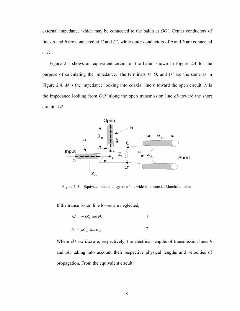
Figure 2.5 shows an equivalent circuit of the balun shown in Figure 2.4 for the
purpose of calculating the impedance. The terminals P, O, and O’ are the same as in
Figure 2.4. M is the impedance looking into coaxial line b toward the open circuit. N is
the impedance looking from OO’ along the open transmission line ab toward the short
circuit at d.
Zab Short
θ abθ ba
b
ZL
Open
Input
Zin
C’
O
O’
C
P
M
N
Figure 2. 5 - Equivalent circuit diagram of the wide band coaxial Marchand balun.
If the transmission line losses are neglected,
bbjZM θcot−= ... 1
,tan ababjZN θ= ... 2
Where θ b and θ ab are, respectively, the electrical lengths of transmission lines b
and ab, taking into account their respective physical lengths and velocities of
propagation. From the equivalent circuit:

10
MNZ
NZZL
Lin +
+= ... 3
bbababL
ababLin jZ
jZZZjZ
Z θθ
θcot
tantan
−+
= ... 4
bbababL
ababL
abab
L
Lin jZ
ZZZjZ
ZZ
ZZ θθ
θ
θ
cottantan
1tan
222
2
22
2 −+
++
= ... 5
If the electrical lengths of line segments b and ab are equal (θ b=θ ab=θ ), and the
characteristic impedance Zab= LZ and Zb= Za =S = Zo, then
θθθ cot))(sin()(sin 22 SZjZZ LLin −+= ... 6
When o90=θ (cotθ =0 and Sinθ = 1) the reactive component of Zin is zero and Zin
equals LZ . While when LZ
S=θ2sin , Zin equal to S (S = Zo). As the lengths of the
transmission lines approach 4λ , i.e., θ goes to
2π the impedance of the short circuit stub
becomes larger while the open stub input impedance gets smaller, and hence the input
impedance Zin converges to ZL. Note that the operating frequency range of the balun is
centered about its resonant frequency. When frequencies are slightly off the center
frequency, the short stub impedance (N) mainly determines Zin since the value of the open
circuit stub impedance (M) is small. Thus larger values of Zab in Figure 2.4 make the
balun more insensitive to frequency.
11
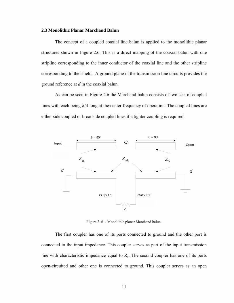
2.3 Monolithic Planar Marchand Balun
The concept of a coupled coaxial line balun is applied to the monolithic planar
structures shown in Figure 2.6. This is a direct mapping of the coaxial balun with one
stripline corresponding to the inner conductor of the coaxial line and the other stripline
corresponding to the shield. A ground plane in the transmission line circuits provides the
ground reference at d in the coaxial balun.
As can be seen in Figure 2.6 the Marchand balun consists of two sets of coupled
lines with each being λ/4 long at the center frequency of operation. The coupled lines are
either side coupled or broadside coupled lines if a tighter coupling is required.
Input
Output 1 Output 2
Open
Za ZbZab
C
d d
θ = 90ο θ = 90ο
ZL
Figure 2. 6 - Monolithic planar Marchand balun.
The first coupler has one of its ports connected to ground and the other port is
connected to the input impedance. This coupler serves as part of the input transmission
line with characteristic impedance equal to Za. The second coupler has one of its ports
open-circuited and other one is connected to ground. This coupler serves as an open

12
transmission line with characteristic impedance equal to Zb. The two strip lines connected
to the load impedance serve as a short-circuit stub (Figure 2.7).
Output 1 Output 2
Zab
d d
ZL
Figure 2. 7 - The bottom two strip lines serve as a short-circuit stub.
In an inhomogeneous medium, where there is partly air and partly dielectric such
as in the case of microstrip and CPW lines, the odd- and even-mode phase velocities are
unequal [4]. The even-mode effective dielectric constant is higher than the odd-mode
effective dielectric constant because the former has less fringing field in the air region.
The result is a lower phase velocity (r
cvε
= ) in the case of the even-mode than in the
case of the odd-mode.
In the case of a directional coupler, the phase velocity inequality will result in
poor directivity [5]. Directivity is a measure of the coupler’s ability to isolate forward and
backward waves, and its directivity performance becomes worse as the coupling is
decreased or as the dielectric permittivity is increased. When analyzing the Marchand
balun as two coupled line sections in cascade, the isolated ports of the couplers will
actually be the two unbalanced ports of the balun. Therefore, any of the undesired effects

13
due to even and odd mode phase velocity inequities contribute to the balun’s amplitude
and phase performance.
2.4 Enhanced Marchand Balun
Two compensation techniques that are used to improve the performance of baluns
in an inhomogeneous medium will be presented. The two techniques proved to provide
compact wide–band baluns.
2.4.1 Compensated Coupled Lines
Compensated coupled lines [6] can be used to design the enhanced Marchand
balun by employing capacitors at each end of the coupled lines, as shown in Figure 2.8.
Input
Output 1 Output 2
Open
Za ZbZab
C
d d
θ = 90ο θ = 90ο
ZL
Figure 2. 8 - Capacitive-compensated Marchand balun.

14
The added capacitors will not affect the even-mode (since the polarity on both strip lines
comprising the coupler is the same) but effectively decrease the odd-mode phase
velocity. This equalization of even and odd mode phase velocity will increase the
directivity and thus provide broadband characteristics with good isolation. The
compensation capacitor is given by [3]
0000 tan41
ϑπ ZfC = ... 7
Where, effe
effo
εεπϑ
20 = , and fo = frequency of operation, Zoo = odd-mode characteristic
impedance, 0ϑ = odd-mode electrical length of the coupled section.
2.4.2 Short Transmission Line Between the Couplers
Compensation can also be accomplished by interconnecting a short transmission
line (Figure 2.9) to a pair of couplers. The variation in the amplitude and phase of the
transmission line will compensate for the amplitude and phase difference of the balun
that is caused by the difference in phase velocities.
Input
Output 1 Output 2
Open
Za ZbZab
`
Short TL
Figure 2. 9 - Compensated Marchand balun using a short transmission line between the two couplers.

15
The short transmission line can be approximated as a capacitor connected
between the ground plane (CPW or microstrip) and the connection point of both couplers
(Figure 2.10). The existence of this capacitor will result in a virtual decrease in the odd-
mode phase velocity of the coupler. This technique compensates for the amplitude and
phase differences of the Marchand balun by creating a circuit that generates differences
in electrical field opposite to those of the balun [7] and thus resulting in cancellation of
the amplitude and phase differences of the balun.
Input
Output 1 Output 2
Open
ZaZb
Zab
Figure 2. 10 - Compensated Marchand balun using a capacitor to ground between the two couplers.

16
2.5 Parallel Connected Marchand Balun
In order to design a broadband Marchand Balun, the balun should have small odd
mode characteristic impedance, which means large coupling capacitance between
individual lines. o
oo CZ 1∝ , where Co is the coupling capacitance [8]. However, it is
difficult to realize a large coupling capacitance because it requires very narrowly-spaced
coupled lines. Two Marchand Baluns can be connected in parallel [8] to solve this
problem (Figure 2.11). The parallel connection of the two baluns will decrease the odd
and even characteristic impedances by 50% and thus provide the required small odd
mode characteristic impedance.
Input
Output 1 Output 2
Open
Za ZbZab
Output 1 Output 2
Open
Za ZbZab
Figure 2. 11 - Parallel-connected Marchand balun.
17
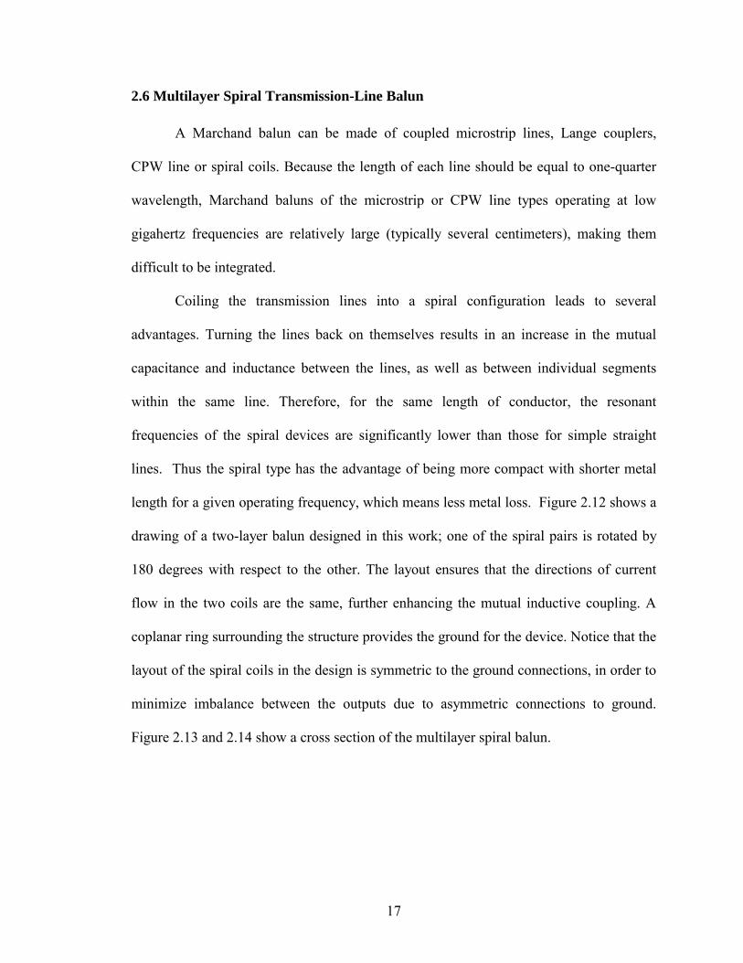
2.6 Multilayer Spiral Transmission-Line Balun
A Marchand balun can be made of coupled microstrip lines, Lange couplers,
CPW line or spiral coils. Because the length of each line should be equal to one-quarter
wavelength, Marchand baluns of the microstrip or CPW line types operating at low
gigahertz frequencies are relatively large (typically several centimeters), making them
difficult to be integrated.
Coiling the transmission lines into a spiral configuration leads to several
advantages. Turning the lines back on themselves results in an increase in the mutual
capacitance and inductance between the lines, as well as between individual segments
within the same line. Therefore, for the same length of conductor, the resonant
frequencies of the spiral devices are significantly lower than those for simple straight
lines. Thus the spiral type has the advantage of being more compact with shorter metal
length for a given operating frequency, which means less metal loss. Figure 2.12 shows a
drawing of a two-layer balun designed in this work; one of the spiral pairs is rotated by
180 degrees with respect to the other. The layout ensures that the directions of current
flow in the two coils are the same, further enhancing the mutual inductive coupling. A
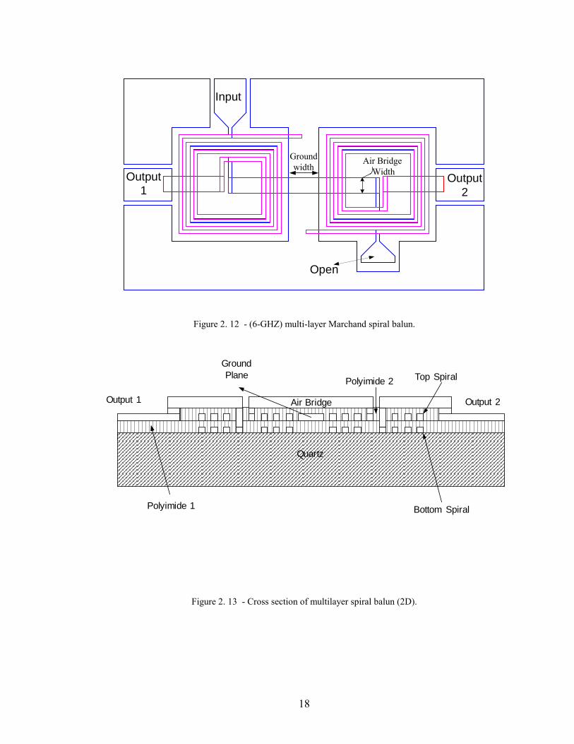
coplanar ring surrounding the structure provides the ground for the device. Notice that the
layout of the spiral coils in the design is symmetric to the ground connections, in order to
minimize imbalance between the outputs due to asymmetric connections to ground.
Figure 2.13 and 2.14 show a cross section of the multilayer spiral balun.
18
Input
Output1
Output2
Open
Groundwidth
Air Bridge Width
Figure 2. 12 - (6-GHZ) multi-layer Marchand spiral balun.
Air Bridge
Quartz
Polyimide 1
Output 1 Output 2
Top Spiral
Bottom Spiral
Polyimide 2
GroundPlane
Figure 2. 13 - Cross section of multilayer spiral balun (2D).

19
Quartz
Polyimide 1
Output 2Output 1
Top Spiral
BottomSpiral
Air Bridge
Ground plane
Polyimide 2
Figure 2. 14 - Cross section of a multi-layer CPW spiral balun. Notice that the input port and the output port were omitted from the drawing for simplicity.

20
Summary
This chapter defined the general problem tackled in the research, that is the
symmetric resonant dipole antenna requires a balanced feed line that can’t be achieved
with a direct connection between the dipole antenna and the regular coaxial transmission
line, and how this problem can be solved using a device called balun (balanced-to-
unbalanced). The work in this chapter gave a description of one of the commonly used
types of baluns, the Marchand Balun. Next it described three of the techniques used to
enhance the performance of the Marchand Balun. At the end of this chapter we presented
the multilayer CPW (coplanar wave guide) spiral Marchand balun.

21
CHAPTER 3 – DESIGN AND ANALYSES OF A MULTILAYER CPW SPIRAL
BALUN
3.1 Introduction
In the previous chapter we have introduced the multilayer spiral CPW balun
(Figure 3.1), which consists of two spiral couplers connected together using an air bridge.
Each coupler consists of two spirals on top of each other in order to obtain tight coupling
(Figure 3.2).
Input
Output1
Output2
Open
Figure 3. 1 - Multi-layer Marchand spiral balun.
Air Bridge

22
Quartz
Output 2Output 1
Top Spiral
Bottom Spiral
Air Bridge
Ground plane
Polyimide
Figure 3. 2 - Cross section of a multi-layer CPW spiral balun. Notice that both the input and open ports were omitted from the drawing for simplicity.
In this chapter we will present the design procedure of the multi-layer CPW spiral
balun. Furthermore, three compensation techniques to enhance the balun performance
will be presented. Those techniques are: introducing a ground plane below the air bridge
and between the two couplers; increasing the capacitance between the air bridge and the
spiral; and varying the capacitance value at the open port.

23
3.2 Design Procedure of the Multilayer CPW Spiral Balun
The required coupling factor k [9] for optimum balun performance can be found
from the following equation:
121
0
+=
ZZ
kL
For a 50 Ω single-ended load impedance and 50 Ω input impedance, k is -4.75dB.
The vertical distance between the two stacked spirals, as well as the horizontal
center-to-center distance between the spirals, are the main parameters to determine the
required amount of coupling. From the simulation for one spiral coupler, the required
parameters (vertical and horizontal offset) can be determined (Figure 3.3).
Figure 3. 3 - Broadside spiral coupler, in the drawing the bottom spiral is horizontally offset to get the required coupling factor.

24
From equation (2.4) (previous chapter):
bbababL
ababLin jZ
jZZZjZ
Z θθ
θcot
tantan
−+
=
The value of Zab should be very large to ensure a broadband balun. Looking from the two
output ports (Figure 3.4) Zab can be considered, as the characteristic impedance exists
between the lower two spirals. It should be mentioned here that the definition of the
characteristic impedance doesn’t apply completely for this case, since the two spirals are
not exactly a real transmission line.
Zab
Output 2Output 1
Zab
Output 2Output 1
Zab
Output 2Output 1
Figure 3. 4 - Equivalent representation of the lower metal spirals.
12
12
CLZ ab ∝
where C12 and L12 are the mutual capacitance per unit length and mutual inductance per
unit length, respectively, between the two spirals. In order to get a high Zab value, C12
should be small and L12 should be high. To increase Zab the distance between the two
spirals should be large enough to decrease the value of C12 and the direction of the

25
currents in the two spirals should be in the same direction to ensure large mutual
inductance between the two bottom spirals.
3.3 Compensation Techniques
3.3.1 Ground plane below the air bridge and between the two couplers
When introducing a ground plane between the two couplers, the performance of
the balun was improved compared to its performance without the ground plane. One valid
explanation for the better performance is that the ground plane, along with the air-bridge
that connects the two couplers and passes over the ground plane, created a capacitance to
ground between the two couplers (Figure 3.5), and as was explained in the previous
chapter, adding a capacitance to ground between the two couplers is one of the
techniques used to enhance the performance of the balun.
Quartz
Polyimide 1
Output 1 Output 2
Top Spiral
BottomSpiral
Polyimide 2GroundPlane
Air Bridge
Figure 3. 5 - Cross section of a multi-layer CPW spiral balun. Notice the area between the ground plane and the air bridge.

26
The capacitance to ground between the two couplers decreases the amplitude and
phase difference over the operational frequency range with only a small change in the
magnitude of S11. When increasing the value of this capacitance, the frequency band
where the acceptable output amplitude difference occurs (typically ~0.5 dB difference
between S21 and S31) will be shifted to a lower frequency range, and the BW will become
smaller. Varying the value of this capacitance is thus a useful tuning mechanism, and
does not induce unwanted degradation in the return loss characteristics (Figure 3.6). In
the following three sub–sections, the values of the parameters in the capacitance equation
(area, height and permittivity) were varied in order to study their effect on the balun
performance.

27
3.3.1.1 Changing the Ground Width and Air Bridge Width
Varying the width of the ground plane between the two couplers or the air bridge
width is one of the methods that could be used to vary the value of the capacitance to
ground. Increasing the capacitance to ground between the two couplers (by increasing
either the ground width or the air bridge width) will decreases the amplitude and phase
difference over the operational frequency range with only a small change in the
magnitude of S11 (Figure 3.6), also the frequency band where the acceptable output
amplitude difference occurs (typically ~0.5 dB difference between S21 and S31) will be
shifted to a lower frequency range (Figure 3.6).
0.00E+0 2.00E+9 4.00E+9 6.00E+9 8.00E+9 1.00E+10
-30.00
-20.00
-10.00
0.00
-0.20
0.20
-0.40
0.00
0.40
Frequency, Hz
dB(S11) dB(S12)-dB(S13)
C = 0.12 pF
C = 0.11 pF
C = 0.1 pF
C = 0.12 pF
C = 0.11 pF
C = 0.1 pF
Figure 3. 6 - Varying the value of the capacitance by varying the ground plane width or the air bridge width to get the desired performance. S11 (solid lines) and S21 (dashed lines).

28
As can be seen in Figure 3.7, by varying the value of C from 0.07 pF to 0.1 pF, the
frequency range where |dB (S21) – dB (S31)| is below 0.5dB shifts to a lower frequency
range with some enhancement on the balun phase difference and the amplitude
imbalance. A larger value of the capacitance will shrink both the amplitude and the phase
bandwidth and will tend to degrade the phase performance (Figures 3.9 to 3.10). From
the shown figures the value of C at which the balun has the best amplitude imbalance and
phase difference occurred at C equal 0.1 pF. Other values of C could also be chosen
depending on the balun bandwidth requirements.
2.00E+9 4.00E+9 6.00E+9 8.00E+9 1.00E+10
-0.20
0.20
-0.40
0.00
0.40
C = 0.07 pF
C = 0.09 pF
C = 0.08 pF
C = 0.1 pF
Frequency, Hz
dB(S12)-dB(S13)
Figure 3.7 – Changing the amplitude imbalance by varying the ground plane width or the air bridge width (increasing C from 0.07pF-to-0.1 pF).

29
0.00E+0 2.00E+9 4.00E+9 6.00E+9 8.00E+9 1.00E+10
170.00
172.00
174.00
176.00
178.00
180.00C = 0.8 pf
C = 0.9 pf
C = 0.1 pf
Frequency, Hz
Phase Difference
Figure 3. 8 - Changing the phase difference by varying the ground plane width or the air bridge width (increasing the value of C from 0.1 pF-to 0.08 pF).

30
0.00E+0 2.00E+9 4.00E+9 6.00E+9 8.00E+9
-0.20
0.20
-0.40
0.00
0.40
C = 0.14 pF
C = 0.16 pF
C = 0.18 pF
Frequency, Hz
dB(S12)-dB(S13)
Figure 3. 9 – Changing the amplitude imbalance by varying the ground plane width or the air bridge width
(increasing the value of C from 0.14pF-to-0.18 pF.

31
0.00E+0 2.00E+9 4.00E+9 6.00E+9 8.00E+9
170.00
172.00
174.00
176.00
178.00
180.00
C = 0.18 pF
C = 0.16 pF
C = 0.14 pF
Frequency, Hz
Phase Difference
Figure 3. 10 - Changing the phase difference by varying the ground plane width or the air bridge width
(increasing the value of C from 0.14 pF-to 0.18 pF).

32
3.3.1.2 Changing air bridge height
To study the effect of the middle capacitor, three similar baluns with different air
bridge heights (H = 2µm, H = 10µm and H = 25µm) were simulated. The performance
when using the highest air bridge balun (smallest capacitance value) was the worst, as
can be seen in Figures 3.11 and 3.12.
2.00E+9 4.00E+9 6.00E+9 8.00E+9 1.00E+10
-0.40
0.00
0.40
Frequency, Hz
dB(S12) - dB(S13)
H = 25e-6
H = 2e-6
H = 10e-6
Figure 3. 11 - Shifting the amplitude imbalance by decreasing the height of the air bridge. For H= 2µm, 10µm and 25µm the BW is 3.63, 4.77 and 1.7 GHz, respectively.

33
0.00E+0 2.00E+9 4.00E+9 6.00E+9 8.00E+9 1.00E+10
170.00
172.00
174.00
176.00
178.00
180.00Ph
ase
Diff
eren
ce
Frequency, Hz
H = 10e-6 m
H = 25e-6 m
H = 2e-6 m
Figure 3. 12 - Shifting the phase difference by decreasing the height of the air bridge.

34
3.3.1.3 Insulator permittivity
The permittivity constant (εr) of the material (polyimide 2, see Figure 3.13) that exists
between the air bridge and the ground plane was varied to study its effect on the balun
performance. A higher value of εr will increase the capacitance between the two couplers
and shift the phase difference and the amplitude imbalance to a lower frequency range
(Figures 3.14 and 3.15). However increasing the value of εr reduced the return loss BW
(Figure 3.16) while the increases in the other capacitance-related parameters (see section
3.3.1.2 and 3.3.1.1) did not have same effect. An explanation for this difference is that
changing the insulator material will affect not only the capacitance between the couplers
but also the characteristics of the CPW lines comprising the balun, as the insulator
material is uniformly deposited over the balun geometry.
Quartz
Polyimide 1
Output 1 Output 2
Top Spiral
BottomSpiral
Polyimide 2GroundPlane
Air Bridge
Figure 3. 13 - Cross section of the multilayer spiral balun. Notice that polyimide 2 in the graph is uniformly deposited over the balun geometry since this balun was simulated using Momentum (ADS) that work better
with uniform material depositing.

35
0.00E+0 2.00E+9 4.00E+9 6.00E+9 8.00E+9 1.00E+10
-0.40
0.00
0.40
Frequency, Hz
dB(S12)-dB(S13)
epsonR = 8
epsonR = 2.6
epsonR = 5
epsonR = 1
Figure 3. 14 - Shifting the amplitude imbalance by increasing the value of εr.

36
0.00E+0 2.00E+9 4.00E+9 6.00E+9 8.00E+9 1.00E+10
170.00
172.00
174.00
176.00
178.00
180.00
Phas
e D
iffer
ence
epsonR = 8
epsonR = 5
epsonR = 1
epsonR = 2.6
Frequency, Hz Figure 3. 15 - Shifting the phase difference by increasing the value of εr.

37
0.00E+0 2.00E+9 4.00E+9 6.00E+9 8.00E+9 1.00E+10
-40.00
-30.00
-20.00
-10.00
0.00
dB(S11)
Frequency, Hz
Legend Title
EpsonR = 1
EpsonR = 8
EpsonR = 5
EpsonR = 2.6
Figure 3. 16 - The change in the return loss by increasing the value of εr.

38
3.3.2 The Capacitance between the air bridge and the spiral
A large capacitance between the air bridge and the spiral strips (Cb) (Figure 3.17)
was used to compensate for the difference in the odd and the even mode phase velocities.
Figure 3.18 presents a comparison between small capacitance and large capacitance
values. The result was better for the case of large capacitance.
Figure 3. 17 - Balun implementing side capacitance techniques for compensation.

39
0.00E+0 2.00E+9 4.00E+9 6.00E+9 8.00E+9 1.00E+10
-0.40
0.00
0.40
170
172
174
176
178
180C = 50 fF
C = 16 fF
C = 50 fF
C = 16 fF
Frequency, Hz
dB(S12)-dB(S13)Phase difference
Figure 3. 18 - Phase difference and amplitude imbalance comparison of the balun when varying the value of the capacitance exists between the air bridge and the spiral strips. Phase difference (dotted lines) and
amplitude imbalance (solid lines).
40
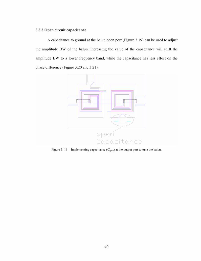
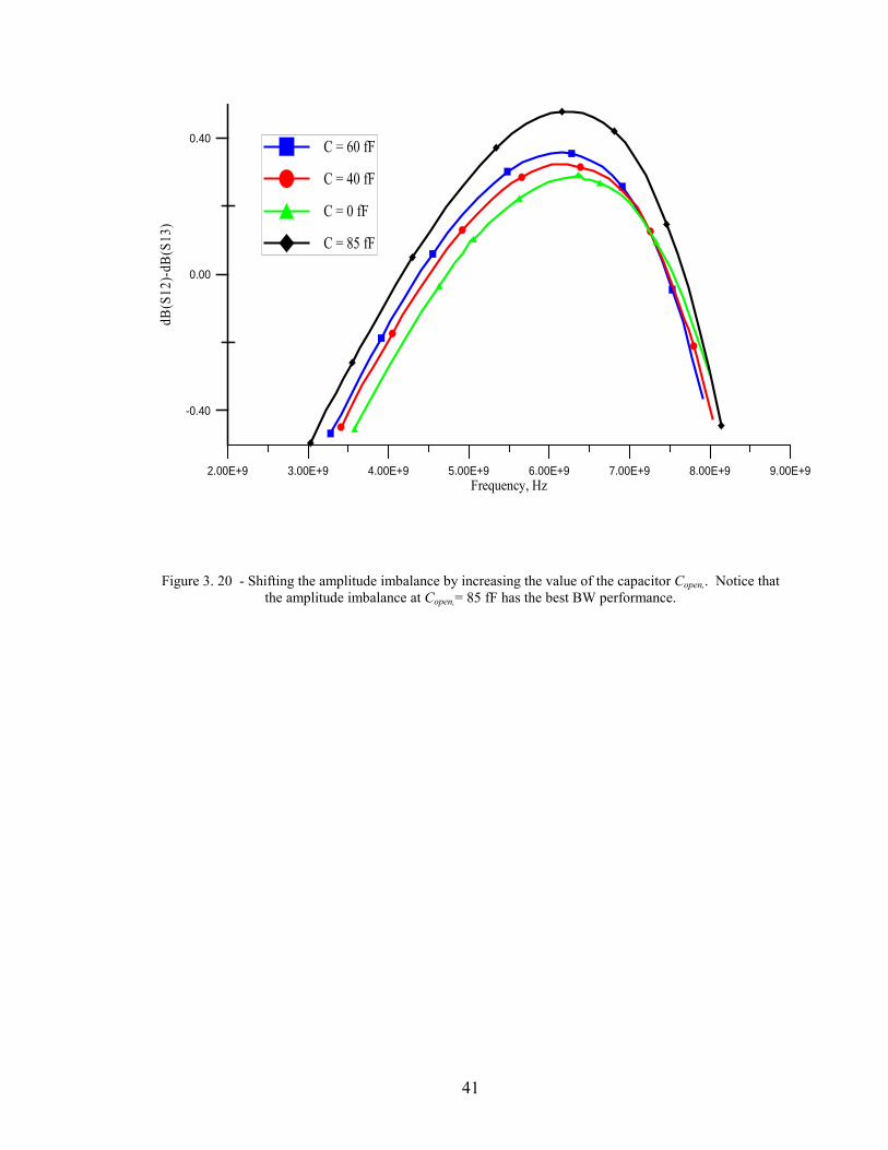
3.3.3 Open circuit capacitance
A capacitance to ground at the balun open port (Figure 3.19) can be used to adjust
the amplitude BW of the balun. Increasing the value of the capacitance will shift the
amplitude BW to a lower frequency band, while the capacitance has less effect on the
phase difference (Figure 3.20 and 3.21).
Figure 3. 19 - Implementing capacitance (Copen) at the output port to tune the balun.
41
2.00E+9 3.00E+9 4.00E+9 5.00E+9 6.00E+9 7.00E+9 8.00E+9 9.00E+9Frequency, Hz
-0.40
0.00
0.40
dB(S
12)-
dB(S
13)
C = 60 fF
C = 40 fF
C = 0 fF
C = 85 fF
Figure 3. 20 - Shifting the amplitude imbalance by increasing the value of the capacitor Copen,. Notice that the amplitude imbalance at Copen,= 85 fF has the best BW performance.

42
0.00E+0 2.00E+9 4.00E+9 6.00E+9 8.00E+9 1.00E+10
170.00
172.00
174.00
176.00
178.00
180.00
Frequency, Hz
C = 85 fF
C = 60 fF
C = 40 fF
Phase Difference
Figure 3. 21 - Phase difference of the balun. Notice that Copen has less effect on the phase difference.

43
3.4 Design Specification
Table 3. 1 - Design parameters of the small and large size baluns, see Figure 3.22 – Figure 3.24 for visualization.
Balun Type Small size balun Large size balun Balun size (mm2) 1.4 x 2.4 3 x 5.6 Air Bridge width (µm) 100 300 Ground width (µm) 200 500 Spiral strip line width (µm) 25 100 Spiral gap width (µm) 25 100 Spiral inner radius (µm) 212 340 Spiral outer radius (µm) 338 635 Horizontal offset (µm) 0 150 Vertical offset (polyimide 1 thickness) (µm)
10 20
Polyimide 2 thickness (µm) 10 10 Polyimide 1 and 2 permittivity
2.6 2.6
Quartz permittivity 3.8 3.8 Quartz thickness (mil) 25 25 Spiral line length λ/4 (mm) 6.7 7.0
Input
Output1
Output2
Open
Groundwidth
Air Bridge Width
Figure 3. 22 - (6 GHz) multilayer CPW spiral Marchand balun.

44
Strip Line Width
Horizontal Offset
Figure 3. 23 - Spiral line coupler.
Gab Width
StripLine
Width
Figure 3. 24 - Spiral line part of the spiral coupler.

45
Summary
In this chapter the design procedure of a multilayer CPW spiral Marchand balun and
three techniques used to enhance the balun performance were presented. The first
technique makes use of the capacitance to ground introduced between the ground plane
and the short interconnect transmission line that is used to connect between the two
couplers. The second technique makes use of the capacitance between the same short
interconnect transmission line and the spiral strip lines. The last technique involves
introducing an extra capacitance to ground at the open port.
The capacitance to ground provided by the short interconnect transmission line
between the two couplers and the ground plane was shown to decrease the phase
difference and the amplitude imbalance between the two balun’s output ports, one valid
explanation for that enhancement is that the capacitance to ground equalized the phase
velocity difference between the odd and the even mode and thus increased the balun
bandwidth. To study the effect of this capacitance on the balun performance, the values
of the parameters in the capacitance equation (area, height and permittivity) were varied.
The study showed that by increasing the capacitance value the operational bandwidth of
the balun was shifted to a lower frequency range and the amplitude and the phase
difference over the operational frequency were minimized with only a small change in
the magnitude of S11 (Return Loss). However, A larger value of the capacitance to ground
will shrink both the amplitude and the phase bandwidth and will tend to degrade the
phase performance.
The other compensation technique, changing the capacitance between the short
interconnection (Air bridge) and spiral strips proved to have good enhancement on the

46
balun performance where the amplitude imbalance bandwidth was doubled by increasing
the capacitance value for example from 16fF to 50 fF. Also increasing the capacitance to
ground at the balun open port proved to be a good technique to tune the amplitude
bandwidth with just small impact on the balun phase difference.

47
CHAPTER 4 – EQUIVALENT MULTILAYER CPW SPIRAL BALUN MODEL
4.1 Introduction
Modeling a microwave device is a useful technique for the design engineer for its
ease in studying the performance of the device under design without the need to run full
wave simulation for each design iteration. In this chapter two models that can be use in
studying the effect on the balun performance due to varying the width of the air bridge,
varying the ground plane width between the two couplers and increasing the capacitance
at the open port were derived. In the first model the two couplers that comprise the balun
were studied by analyzing the two couplers individually using a full wave simulation
software (Momentum) and then combining the results in a circuit simulator. In the second
model, a lumped elements model for each coupler was derived through circuit
optimization against the full wave simulation results obtained using Momentum (ADS)
and then the two models were combined in one single model that represent the balun.

48
4.2 Equivalent Split model for the Multilayer spiral Balun
The two couplers that comprise the balun were analyzed individually and the
derived [S] parameters were combined in a circuit simulator. The representation
developed from this approach will be termed the ‘split model’. Figure 4.1 shows a
diagram of the full balun, Figure 4.2 shows the two separated couplers, and Figure 4.3
shows the circuit representation of the split model.
Figure 4. 1 - Full balun diagram.
(a) (b)
Figure 4. 2 - The two Separated Couplers (a) left coupler (b) right coupler. The arrows point to the CPW transmission line added to enable proper simulation of the circuits in Momentum; these lines were de-
embedded when circuit simulations were performed.

49
De-embed Boxs
TermTerm4
TermTerm5
S3PSNP1
2
3 Ref
1
Deembed2SNP4
21
Ref
Deembed2SNP3
21
Ref
S2PSNP2
21
RefTermTerm6
Figure 4. 3 - Split model representation of the Marchand balun.
One of the main purposes behind deriving the split model was to study the effect
of the capacitance to ground between the two couplers without the need to run the full
wave simulation for each changes in the capacitance parameters. Hence a variable
capacitor to ground C was added at the connection point between the two couplers
(Figure 4.4), the results shown in Figure 4.5, 4.6 and 4.7 show that the performance of the
split model matched the full-wave simulation results of the balun when C is equal to zero
(no ground plane bellow the air bridge in the balun circuit). However, increasing the line
width of the air-bridge from 25µ to 100µ above the ground plane, which corresponds to
adding a 50 fF capacitance to ground at the connection point between the two couplers in
the split model didn’t achieve the same result even so it enhanced the balun performance.

50
The reason for the difference in the performance between the full-wave results and the
split model is due to the fact that increasing the air-bridge width will also introduce
additional capacitance between the air bridge and the spiral strips and as was shown in
section 3.3.2 this type of capacitance served as a compensation technique. Simply
changing the capacitance value in the split model didn’t not introduce the same effect.
Figure 4. 4 - Split model representation of the Marchand balun for the purpose of studying the effect of the capacitance to ground between the two couplers. The de-embed boxes negated the CPW lines denoted in
Figure 4.2.
S2PSNP2
21 Ref
1 2
3
1
Deembed2 SNP3File="CPTL.ds"
2
Ref
1 2
3
1
CC1C=C pF
2
1Deembed2SNP4File="CPTL.ds"
21
Ref
1 2
3
1
TermTerm3
Z=50 OhmNum=3
1
2
Term Term2
Z=50 Ohm Num=2 1
2
TermTerm1
Z=50 OhmNum=1
1
2
1 111
S3PSNP1
2
3 Ref
11 2
3 41 Deembed boxs

51
0.00E+0 2.00E+9 4.00E+9 6.00E+9 8.00E+9
170.00
172.00
174.00
176.00
178.00
180.00
Split Model
Full Balun
Frequency, Hz
Phase Difference
Figure 4. 5 Similar phase difference performance between the split model and the full-wave simulation result for C=0 pF.

52
4.00E+9 4.40E+9 4.80E+9 5.20E+9 5.60E+9 6.00E+9
-0.40
0.00
0.40
Split Model
Full Balun
Frequency, Hz
dB(S12)-dB(S13)
Figure 4. 6 Similar amplitude imbalance performance between the split model and the full-wave simulation result for C=0 pF.

53
0.00E+0 4.00E+9 8.00E+9
-50.00
-40.00
-30.00
-20.00
-10.00
0.00
Frequency, Hz
dB(S11)
Split Model
Full Balun
Figure 4. 7 Similar return loss performance between the split model and the full-wave balun simulation
result.

54
3.00E+9 4.00E+9 5.00E+9 6.00E+9 7.00E+9 8.00E+9
-0.40
0.00
0.40
Frequency, Hz
dB(S12)-dB(S13)
Split Model
Full Balun
Figure 4. 8 Comparison in the amplitude imbalance performance between the split model and the full-wave balun simulation result when adding a 0.05 pF capacitor to ground between the two couplers.

55
To get an optimum capacitance value, the capacitance value in the split model can
be tuned using the circuit schematic in ADS. The performances of the balun return loss,
phase difference and amplitude imbalance can be derived as a function of the capacitance
value as shown in Figure 4.9, Figure 4.10 and Figure 4.11.
0.00E+0 2.00E+9 4.00E+9 6.00E+9 8.00E+9 1.00E+10
-0.80
-0.40
0.00
0.40
0.80
Frequency,Hz
dB(S12)-dB(S13)
C = 0.2 pF
C = 0.17 pF
C = 0.14 pF
C = 0.11 pF
C = 0.08 pF
C = 0.05 pF
Figure 4. 9 The change of amplitude imbalance performance by varying the value of C from 0.05 pF-to-
0.2pF.

56
0.00E+0 2.00E+9 4.00E+9 6.00E+9 8.00E+9 1.00E+10
170.00
172.00
174.00
176.00
178.00
180.00
C = 0.17pF
C = 0.08pF
C = 0.05pF
C = 0.2pF
Frequency,Hz
Phase Difference
Figure 4. 10 The change of phase difference performance by varying the value of C from 0.05 pF-to-0.2 pF.

57
0.00E+0 2.00E+9 4.00E+9 6.00E+9 8.00E+9 1.00E+10
-40.00
-30.00
-20.00
-10.00
0.00
C = 0.05pF
C = 0.08pF
C = 0.11pF
C = 0.14pF
C = 0.17pF
C = 0.2pF
Frequency,Hz
dB(S11)
Figure 4. 11 The change in the magnitude of dB|S11| by varying the value of C from 0.05 pF-to-0.2 pF.
As can be seen in figure 4.9 and 4.10 there is a point at which the amplitude
imbalances and phase difference are optimum. Notice that S11 (Figure 4.11) is less
sensitive than the phase difference and the amplitude imbalance to the change in the
value of C. This fact can be used to adjust the center frequency by shifting the frequency
range where the amplitude imbalance ( |dB (S21) – dB (S31)| ) is less than 0.5dB and the
phase difference (|Phase (S21) – Phase (S31)|) is 180 +/- 5 degrees or less to the range
where dB|S11| is minimum.

58
4.3 Equivalent Lumped Elements Model for the Multilayer Spiral Balun
A lumped element model that represents the performance of the multilayer CPW
spiral balun over the desired frequency range (1-8 GHz) was developed and
characterized. The lumped element model is an important tool in understanding different
parameters that comprise the balun. The lumped element model can also help analyzing
the effect of previously discussed compensation techniques such as varying the
capacitance to ground at the point between the two couplers, varying the air bridge width
over the spiral strips and adding extra capacitance to ground at the open port of the balun.
Since the balun consists of two couplers, a lumped element model was developed for
each. The first model represents the left hand side coupler that has three ports (Figure
4.12 and 4.14). The second model represents the right hand side coupler (Figure 4.13 and
4.15) that has two ports. Figure 4.16 shows the balun equivalent lumped element model
after connecting the two couplers models together; an ideal capacitor was added between
the connection point between the two models and ground to represent the capacitance to
ground resulted from the air bridge and the ground plane.
The lumped element model for a one side spiral coupler consists of seven broadside
couplers each one representing a half turn in the real spiral couplers, The capacitors (Cb)
represent the capacitance between half portion of the air bridge that connect between the
two couplers and each strip of the upper spiral below that air bridge. The capacitors (Ca)
represent the capacitance between each strip of the upper spiral and the air bridge that
connects the bottom spiral to the output port. Copen represents the capacitance to ground at
the open port of the balun. Table 4.1 shows the values of the equivalent model optimized-
parameters.

59
Figure 4. 12 - Left side coupler that is part of the balun.
Figure 4. 13 - Right side coupler that is part of the balun.

60
CC b _ 2
CC b _ 1
CC b _ 3
C L IN PT L 1
C L IN PT L 2
C L IN PT L 3
C L IN PT L 4
C L IN PT L 5
C L IN PT L 6
C L IN PT L 7
C P WC P W 1
P o r tP 3
C P WC P W 2
P o r tP 2
CC a _ 1
CC a _ 2
CC a _ 3
P o r tP 1
C P WC P W 3
Figure 4. 14 - Equivalent circuit model of the left hand side coupler. The capacitors (Cb) represent the capacitance between the right air bridge and every strip of the upper spiral that passes below that air bridge.
The capacitors (Ca) represent the capacitance between the strip lines of the upper spiral and the left air bridge that connects the bottom spiral to the output port.

61
CC o p e n
CC a _ 3
CC a _ 2
CC a _ 1
CC b _ 3
CC b _ 2
CC b _ 1
P o r tP 2
P o r tP 1
C L I N PT L 2
C L I N PT L 7
C L I N PT L 6
C L I N PT L 5
C L I N PT L 4
C L I N PT L 3
C L I N PT L 1
C P WC P W 1
C P WC P W 2
Figure 4. 15 - Equivalent circuit modal of the right hand side coupler. Notice that the capacitors (Cb)
represent the capacitance resulted between the left air bridge and every single strip of the upper spiral that pass below that air bridge, also notice that the capacitors (Ca) represent the capacitance between every
single strip of the upper spiral and the right air bridge that connects the bottom spiral to the output port, the capacitance Copen represent the equivalent open circuit capacitance.

62
CC2C=00.1 pF
2
1
1
2portCouplerOptimazation_glopal_AbX5
1 2
3portCouplerOptimazation_glopal_AbX4
1 2
3
TermTerm1
Z=50 OhmNum=1
1
2
1
TermTerm2
Z=50 OhmNum=2
1
2
1
TermTerm3
Z=50 OhmNum=3
1
21
Figure 4. 16 - The full balun equivalent circuit model consisting of the two optimized coupler models.
Table 4. 1 - The optimized parameter values of the equivalent model.
Ca (Ca_1 = Ca_2 = Ca_3 =) 15.0328 fF
Cb (Cb_1 = Cb_2 = Cb_3 =) 15.0 fF
Copen 30.0 fF
C 50 fF
Zoo 45.6124 Ω
Zoe 477.901 Ω
εoo 3.79986
εoe 2.39395
L (length of each coupler) .855 mm
Attenuation even 0.0251977
Attenuation odd 68.6089

63
When applying the same capacitance to ground between the two couplers for both the
equivalent model and the split model the results of both models matched very will with
each other. When applying the corresponding capacitance value to the full balun circuit
its full-wave simulation results also matched with the two models results. Figures 4.17 –
4.21 show comparisons of the value of dB (S11), dB (S12), dB (S13), phase (S12) and phase
(S13) when the value of the capacitance to ground equal .05 pF. The physical dimensions
of the full small size balun are presented in Table 3.1. Notice from the result that at high
frequency range both models result don’t match completely with the full-wave simulation
result, since lumped element models usually work better at low frequency.

64
0.00E+0 4.00E+9 8.00E+9
-30.00
-20.00
-10.00
0.00
Frequency, Hz
dB(S11)
Equivalent Model
Split Model
Full Balun
Figure 4. 17 – Comparisons of the value of dB (S11), equivalent model versus full balun and split model.

65
0.00E+0 4.00E+9 8.00E+9Frequency, Hz
-40.00
-30.00
-20.00
-10.00
0.00
dB(S
12)
Equivalent Model
Split Model
Full Balun
Figure 4. 18 – Comparisons of the value of dB (S12), equivalent model versus full balun and split model.

66
0.00E+0 4.00E+9 8.00E+9Frequency, Hz
-40.00
-30.00
-20.00
-10.00
0.00
dB(S
13)
Equivalent Model
Split Model
Full Balun
Figure 4. 19 – Comparisons of the value of dB (S13), equivalent model versus full balun and split model.

67
0.00E+0 4.00E+9 8.00E+9Frequency, Hz
-200.00
-100.00
0.00
100.00
200.00
Phas
e(S1
2)Equivalent Model
Split Model
Full Balun
Figure 4. 20 – Comparisons of the value of Phase (S12), equivalent model versus full balun and split model.
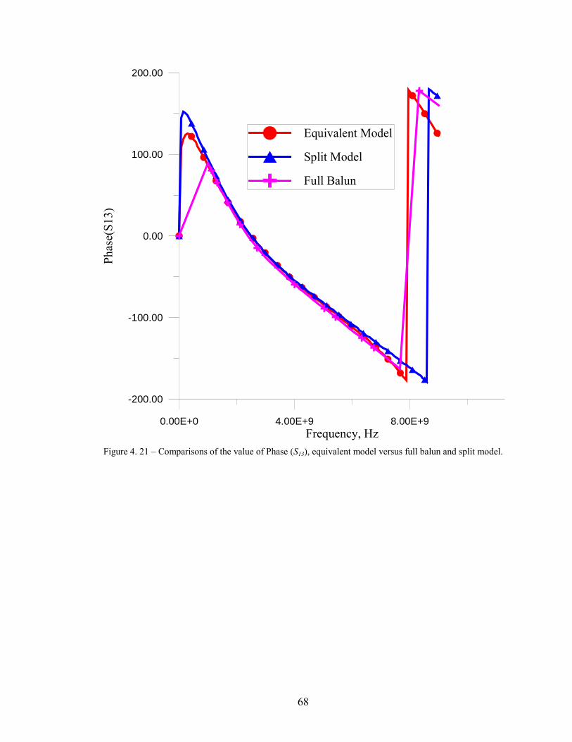
68
0.00E+0 4.00E+9 8.00E+9Frequency, Hz
-200.00
-100.00
0.00
100.00
200.00
Phas
e(S1
3)
Equivalent Model
Split Model
Full Balun
Figure 4. 21 – Comparisons of the value of Phase (S13), equivalent model versus full balun and split model.

69
Summary
In this chapter two multilayer CPW spiral Marchand balun models were presented.
The two models helped in analyzing the balun physical parameters and in studying the
effect of introducing different lumped elements on the balun circuit to derive the
techniques required to compensate between the difference in the phase velocity of the
odd mode and the even mode. In the first model (split model) the two couplers that
comprise the balun were studied by analyzing the two couplers individually using a full
wave simulation software (Momentum) and then combining the results in a circuit
simulator, this model was used to study the effect of the capacitance to ground (exist
between the two couplers) on the balun performance. The study showed good agreement
between the model (split model) results and results obtained using the full wave
simulation (Momentum). In the second model (equivalent model) the lumped element
model for each coupler were combined in one lumped element model. Each coupler
model was derived through circuit optimization against the full wave simulation results
obtained using Momentum (ADS). The equivalent model result were compared with the
results obtained from both the full-wave simulation (Momentum) and the split model, the
comparisons showed good agreement.
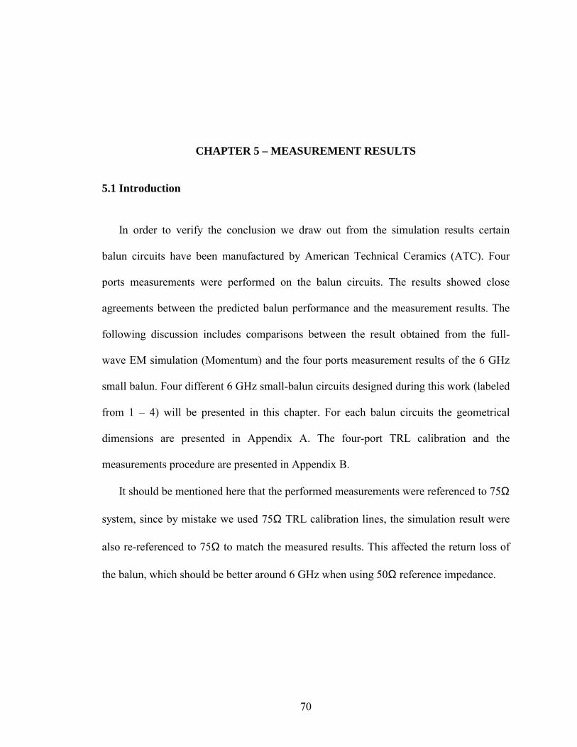
70
CHAPTER 5 – MEASUREMENT RESULTS
5.1 Introduction
In order to verify the conclusion we draw out from the simulation results certain
balun circuits have been manufactured by American Technical Ceramics (ATC). Four
ports measurements were performed on the balun circuits. The results showed close
agreements between the predicted balun performance and the measurement results. The
following discussion includes comparisons between the result obtained from the full-
wave EM simulation (Momentum) and the four ports measurement results of the 6 GHz
small balun. Four different 6 GHz small-balun circuits designed during this work (labeled
from 1 – 4) will be presented in this chapter. For each balun circuits the geometrical
dimensions are presented in Appendix A. The four-port TRL calibration and the
measurements procedure are presented in Appendix B.
It should be mentioned here that the performed measurements were referenced to 75Ω
system, since by mistake we used 75Ω TRL calibration lines, the simulation result were
also re-referenced to 75Ω to match the measured results. This affected the return loss of
the balun, which should be better around 6 GHz when using 50Ω reference impedance.

71
5.2 Balun number 1
For a small balun circuit working at 6 GHz (Figure 5.1) that has 304µm ground width
and 100µm air bridge width (capacitance to ground between the two couplers equal 70
fF), the comparison results are shown in Figure 5.2 - 5.9.
Input
Output1
Output2
Open
Groundwidth
Air Bridge Width
Figure 5. 1 - (6-GHZ) multi-layer spiral Marchand balun.

72
0.00E+0 4.00E+9 8.00E+9Frequency, Hz
-3.00
-2.00
-1.00
0.00
1.00
2.00
dB(S
12)-
dB
(S13
)
Figure 5. 2 - Amplitude imbalance of a balun circuit, measurements versus full-wave EM simulation data.

73
0.00E+0 4.00E+9 8.00E+9Frequency, Hz
-0.40
0.00
0.40dB
(S12
)- d
B(S
13)
Figure 5. 3 - Amplitude imbalance of a balun circuit, measurements versus full-wave EM simulation data
on a different scale.

74
0.00E+0 4.00E+9 8.00E+9Frequency, Hz
140.00
150.00
160.00
170.00
180.00
Phas
e D
iffer
ence
Figure 5. 4 - Phase difference of a balun circuit, measurements versus full-wave EM simulation data.

75
0.00E+0 4.00E+9 8.00E+9
-16.00
-12.00
-8.00
-4.00
0.00
dB(S
11)
Frequency, Hz
Measured Data
Simulated Data
Figure 5. 5 - Return loss (S11) of the balun circuit, measurements versus full-wave EM simulation data.
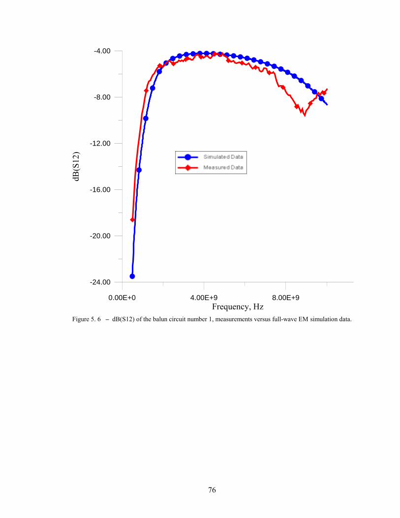
76
0.00E+0 4.00E+9 8.00E+9Frequency, Hz
-24.00
-20.00
-16.00
-12.00
-8.00
-4.00
dB(S
12)
Figure 5. 6 – dB(S12) of the balun circuit number 1, measurements versus full-wave EM simulation data.

77
0.00E+0 4.00E+9 8.00E+9Frequency, Hz
-30.00
-20.00
-10.00
0.00
dB(S
13)
Figure 5. 7 – dB(S13) of the balun circuit number 1, measurements versus full-wave EM simulation data.
78
0.00E+0 4.00E+9 8.00E+9Frequency, Hz
-200.00
-100.00
0.00
100.00
200.00
Phas
e(S1
2)
Simulated Data
Measured Data
Figure 5. 8 – Phase(S12) of the balun circuit number 1, measurements versus full-wave EM simulation
data.

79
0.00E+0 4.00E+9 8.00E+9Frequency, Hz
-200.00
-100.00
0.00
100.00
200.00
Phas
e(S1
3)
Figure 5. 9 – Phase(S13) of the balun circuit number 1, measurements versus full-wave EM simulation
data.

80
5.3 Balun number 2
For a small balun circuit working at 6 GHz (Figure 5.1) that has 200µm ground
width and 50µm air bridge width (capacitance to ground between the two couplers equal
23 fF), the comparison results are shown in Figure 5.10 - 5.17.
0.00E+0 2.00E+9 4.00E+9 6.00E+9 8.00E+9 1.00E+10Frequency,Hz
-4.00
-2.00
0.00
2.00
4.00
dB(S
12)-
dB(S
13)
Measured Data
Simulated Data
Figure 5. 10 - Amplitude imbalance of a balun circuit, measurements versus full-wave EM simulation data.

81
3.00E+9 4.00E+9 5.00E+9 6.00E+9 7.00E+9 8.00E+9 9.00E+9Frequency,Hz
-0.40
0.00
0.40
dB(S
12)-
dB(S
13) Measured Data
Simulated Data
Figure 5. 11 - Amplitude imbalance of a balun circuit, measurements versus full-wave EM simulation data
on a different scale.

82
0.00E+0 2.00E+9 4.00E+9 6.00E+9 8.00E+9 1.00E+10Frequency,Hz
100.00
120.00
140.00
160.00
180.00Ph
ase
Def
eren
ce
Simulated Data
Measured Data
Figure 5. 12 - Phase difference of a balun circuit, measurements versus full-wave EM simulation data.
Phase Difference

83
0.00E+0 4.00E+9 8.00E+9Frequency, Hz
-20.00
-16.00
-12.00
-8.00
-4.00
0.00
dB(S
11)
Figure 5. 13 - Return loss (S11) of the balun circuit, measurements versus full-wave EM simulation data.

84
0.00E+0 2.00E+9 4.00E+9 6.00E+9 8.00E+9 1.00E+10Frequency,Hz
-30.00
-20.00
-10.00
0.00
dB(S
12)
Simulated Data
Measured Data
Figure 5. 14 – dB(S12) of the balun circuit number 2, measurements versus full-wave EM simulation data.

85
0.00E+0 2.00E+9 4.00E+9 6.00E+9 8.00E+9 1.00E+10Frequency,Hz
-30.00
-20.00
-10.00
0.00
dB(S
13)
Simulated Data
Measured Data
Figure 5. 15 – dB(S13) of the balun circuit number 2, measurements versus full-wave EM simulation data.

86
0.00E+0 2.00E+9 4.00E+9 6.00E+9 8.00E+9 1.00E+10Frequency,Hz
-200.00
-100.00
0.00
100.00
200.00
Phas
e(S1
2)
Simulated Data
Measured Data
Figure 5. 16 – Phase(S12) of the balun circuit number 2, measurements versus full-wave EM simulation
data.
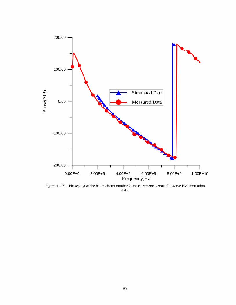
87
0.00E+0 2.00E+9 4.00E+9 6.00E+9 8.00E+9 1.00E+10Frequency,Hz
-200.00
-100.00
0.00
100.00
200.00
Phas
e(S1
3) Simulated Data
Measured Data
Figure 5. 17 – Phase(S13) of the balun circuit number 2, measurements versus full-wave EM simulation
data.

88
5.4 Balun number 3
For a small balun circuit working at 6 GHz (Figure 5.18) that has 204µm ground
width and 300µm air bridge width (capacitance to ground between the two couplers equal
140 fF), the comparison results are shown in Figure 5.19 - 5.26.
Figure 5. 18 - (6-GHZ) multi-layer Marchand spiral balun. Notice the air bridge cross shape above the
ground plane.

89
0.00E+0 2.00E+9 4.00E+9 6.00E+9 8.00E+9 1.00E+10Frequency,Hz
-4.00
0.00
4.00
8.00dB
(S12
)-dB
(S13
)
Measured Data
Simulated Data
Figure 5. 19 - Amplitude imbalance of a balun circuit, measurements versus full-wave EM simulation data.

90
0.00E+0 2.00E+9 4.00E+9 6.00E+9 8.00E+9Frequency,Hz
-0.40
0.00
0.40dB
(S12
)-dB
(S13
)Measured Data
Simulated Data
Figure 5. 20 - Amplitude imbalance of a balun circuit, measurements versus full-wave EM simulation data
on different scale.

91
0.00E+0 2.00E+9 4.00E+9 6.00E+9 8.00E+9 1.00E+10Frequency,Hz
100.00
120.00
140.00
160.00
180.00
Phas
e D
efer
ence Simulated Data
Measured Data
Figure 5. 21 - Phase difference of a balun circuit, measurements versus full-wave EM simulation data.
Phase Difference

92
0.00E+0 4.00E+9 8.00E+9Frequency, Hz
-25.00
-20.00
-15.00
-10.00
-5.00
0.00
dB(S
11)
Figure 5. 22 - Return loss (S11) of the balun circuit, measurements versus full-wave EM simulation data.

93
0.00E+0 2.00E+9 4.00E+9 6.00E+9 8.00E+9 1.00E+10Frequency,Hz
-30.00
-20.00
-10.00
0.00
dB(S
12)
Simulated Data
Measured Data
Figure 5. 23 – dB(S12) of the balun circuit number 3, measurements versus full-wave EM simulation data.

94
0.00E+0 2.00E+9 4.00E+9 6.00E+9 8.00E+9 1.00E+10Frequency,Hz
-30.00
-20.00
-10.00
0.00
dB(S
13)
Simulated Data
Measured Data
Figure 5. 24 – dB(S13) of the balun circuit number 3, measurements versus full-wave EM simulation data.

95
0.00E+0 2.00E+9 4.00E+9 6.00E+9 8.00E+9 1.00E+10Frequency,Hz
-200.00
-100.00
0.00
100.00
200.00
Phas
e(S1
2)
Simulated Data
Measured Data
Figure 5. 25 – Phase(S12) of the balun circuit number 3, measurements versus full-wave EM simulation
data.

96
0.00E+0 2.00E+9 4.00E+9 6.00E+9 8.00E+9 1.00E+10Frequency,Hz
-200.00
-100.00
0.00
100.00
200.00
Phas
e(S1
3)
Simulated Data
Measured Data
Figure 5. 26 – Phase(S13) of the balun circuit number 3, measurements versus full-wave EM simulation
data.

97
5.5 Balun number 4
For a small balun circuit working at 6 GHz (Figure 5.27) that has 204µm ground
width and 50µm air bridge width (Capacitance to ground between the two couplers equal
23 fF), but with capacitance between the air bridge and the spiral strips equal to 16fF at
each side. The comparison results are shown in Figure 5.28 - 5.34.
Figure 5. 27 - Balun implementing side capacitance techniques for compensation.

98
0.00E+0 2.00E+9 4.00E+9 6.00E+9 8.00E+9 1.00E+10Frequency,Hz
-4.00
0.00
4.00
8.00dB
(S12
)-dB
(S13
)
Measured Data
Simulated Data
Figure 5. 28 - Amplitude imbalance of a balun circuit, measurements versus full-wave EM simulation data.

99
0.00E+0 2.00E+9 4.00E+9 6.00E+9 8.00E+9 1.00E+10Frequency,Hz
100.00
120.00
140.00
160.00
180.00
Phas
e D
efer
ence
Simulated Data
Measured Data
Figure 5. 29 - Phase difference of a balun circuit, measurements versus full-wave EM simulation data.
Phase Difference

100
0.00E+0 4.00E+9 8.00E+9Frequency, Hz
-25.00
-20.00
-15.00
-10.00
-5.00
0.00
dB(S
11)
Figure 5. 30 - Return loss (S11) of the balun circuit, measurements versus full-wave EM simulation data.

101
0.00E+0 2.00E+9 4.00E+9 6.00E+9 8.00E+9 1.00E+10Frequency,Hz
-30.00
-20.00
-10.00
0.00
dB(S
12)
Simulated Data
Measured Data
Figure 5. 31 – dB(S12) of the balun circuit number 4, measurements versus full-wave EM simulation data.

102
0.00E+0 2.00E+9 4.00E+9 6.00E+9 8.00E+9 1.00E+10Frequency,Hz
-30.00
-20.00
-10.00
0.00
dB(S
13)
Simulated Data
Measured Data
Figure 5. 32 – dB(S13) of the balun circuit number 4, measurements versus full-wave EM simulation data.

103
0.00E+0 2.00E+9 4.00E+9 6.00E+9 8.00E+9 1.00E+10Frequency,Hz
-200.00
-100.00
0.00
100.00
200.00
Phas
e(S1
2)
Simulated Data
Measured Data
Figure 5. 33 – Phase(S12) of the balun circuit number 4, measurements versus full-wave EM simulation
data.

104
0.00E+0 2.00E+9 4.00E+9 6.00E+9 8.00E+9 1.00E+10Frequency,Hz
-200.00
-100.00
0.00
100.00
200.00
Phas
e(S1
3) Simulated Data
Measured Data
Figure 5. 34 – Phase(S13) of the balun circuit number 4, measurements versus full-wave EM simulation
data.

105
5.6 Balun Performance.
A previous paper on Marchand baluns by Yeong J, Yoon and Robert C. Frye
reported a small size CPW multilayer spiral fabricated on silicon with good performance
- RL (return loss) better than 17dB in the frequency range from 1.6 GHz – 4.1 GHz, and
better than 39dB RL around 1.9 GHz. The amplitude imbalance was less than 0.3 dB
through the whole band, and the phase difference was less than 2º over the frequency
range 1.6-2.6 GHz. The overall size is 1.2 x 2.3 mm² [10]. The same authors reported a
similar topology spiral balun, fabricated on glass and high resistivity silicon [11]. The
frequency response was similar in both cases since the mutual coupling capacitance
occurred in the insulator between the spirals of the couplers. The ratio of the conductor
width to pitch (the conductor strip width plus the width of the gap between two adjacent
spiral strips) fell between 0.4-0.6 to get good return loss and good amplitude and phase
difference for a 50Ω input impedance and a 50Ω load impedance. The center frequency
of the 3dB BW ranged from 1.2 to 3.5 GHz, while the relative BW normalized by the
center frequency was typically ~ 1.48. Return loose (RL) at the center frequency in all
cases was in the range of 13-18 dB. Amplitude imbalance within the OBW (operational
bandwidth) was less than 0.9dB for the glass substrate balun and less than 0.5dB for the
silicon substrate balun.
In [12] a balun built using a microstrip transmission line and a short transmission line
between the two couplers to compensate for the phase and amplitude imbalance was
described. They reported a 2-6 GHz bandwidth with amplitude imbalance of 0.2dB and
phase difference of 10º, and an overall size equal to 0.7 x 1.5 mm².

106
We developed a new CPW multilayer spiral Marchand balun based on the techniques
in [10, 12]. Both the simulation and measurement results showed a 75% bandwidth
around the center frequency of 5.5 GHz with return loss better than 14dB. The amplitude
and phase difference are less than 0.5dB and 3o, respectively. Overall balun size is 1.4 x
2.4 mm² the balun has 25µm minimum line width and 25µm minimum spacing between
adjacent strips. The balun Operational BW (OBW) is 4 GHZ. The center frequency λ/4 (6
GHz) corresponds to a spiral line length equal to 6.7 mm. The vertical offset distance that
gives the required coupling factor was found to be 0.01 mm without the need to vary the
horizontal offset. Another larger balun size (3 x 5.6 mm²) was designed with minimum
line and gap widths of 100µm, the balun OBW equal to 2.0 GHZ around 4 GHZ with
return loss (RL) better than 11 dB. The amplitude imbalance and phase difference are 0.5
dB and 10o, respectively.
Table 5. 1 - Comparison between the previously reported balun performance results and our balun design results (the small and the large size baluns).
Balun type OBW (GHz)
Phase Difference (Degree)
Amplitude Imbalance (+/- dB)
Frequency Range (GHz)
Size (mm²)
Robert CPW balun [10]
2.5 3o - 6o 0.2 1.6 – 4.1 1.2 x 2.3
Microstrip balun [12]
4 10o 0.2 2 - 6 0.7 x 1.5
Small balun Range 1 4 3o 0.5 4 - 8 1.4 x 2.4 Small balun Range 2 5.5 5o 0.5 5.5 -10 1.4 x 2.4 The large size balun 2 10o 0.5 3 -5 3 x 5.6

107
Summary
This chapter presented comparisons between the full-wave EM simulation results,
obtained using Momentum, and the results of the four ports measurements of the small
size balun circuit. Both results showed good agreement with each other, which supports
the validity of other results obtained using Momentum. At the end of this chapter
previously published balun designs were compared with the two balun designs (small
balun and large balun) presented in this work. The comparison showed that the small size
balun has very good performance over the desired frequency range.

108
CHAPTER 6 – COMPARISON OF MoM AND FDTD
6.1 Introduction
Before the advent of high-speed computers, it was advantageous to spend
considerable effort to manipulate solutions analytically into a form, which minimized the
subsequent computational effort. Nowadays with the high-speed computers it is more
convenient to use simple analytical methods without worrying about the amounts of
computation. Many numerical techniques have been derived to solve Maxwell’s
differential or integral equations [13]- [15] such as, finite-difference time-domain
(FDTD) and method of moments (MoM).
In this chapter two commercial softwares, Momentum (MoM) and Empire
(FDTD), were applied to the 6 GHz balun and compared in terms of accuracy of
scattering parameters, CPU speed and memory usage. This chapter is organized in the
following way: Sections 6.1 and 6.2 briefly introduce the FDTD and MoM techniques
and, section 6.3 discusses the numerical results.

109
6.2 Finite-Difference Time-Domain method (FDTD)
The FDTD as introduced by Yee [16], has been proven to be convenient and
simple tool for time domain analysis and for various electromagnetic scattering problems.
The basis of the FDTD algorithm is the Maxwell’s curl equations. For uniform, isotropic
and homogenous media Maxwell’ s curl equation is given as:
tHE∂∂−=×∇ µ
tEEH
∂∂+=×∇ εσ
where E, H,ε , µ , and σ are the electric field, magnetic field, permittivity, permeability,
and conductivity, respectively. The central difference approximation is given by the
following equation as a function of time and space [16]
[ ] [ ]nkjiz
nkjiz
nkjiy
nkjiy
nkjix
nkjix EE
ytEE
ztHH )1,,1()1,,1(),1,()1,1,(
2/1)1,1,(
2/1)1,1,( +−+++++
−++
+++ −
∆∆−−
∆∆+=
µµ
for Hx and similar equations for the Ex, Ey, Ez, Hy and Hz components. The scattering
parameters as a function of the frequency can be obtained from the time-domain solutions
E and H fields using Fourier transform (FT).
Stability restriction limits the time increment t∆ . The maximum time step that
that can be used to avoid numerical instability as a function of the grid sizes x∆ , y∆ , and
z∆ is given by the following formula:
2/1
222max
1111−
∆+
∆+
∆<∆
zyxvt
where vmax is the maximum speed of the electromagnetic wave inside the modeled
martial.

110
Since it is not possible to use infinite grid size the solution domain for the FDTD
must be terminated probably by absorbing boundaries around the grid [17][18], in order
to reduce the computational cost.
6.3 Method of Moments
The method of Moments (MoM) [14] can be used for solving both differential and
integral equations. After discretizing the required integral equation into a matrix
equation, evaluates the matrix elements, and solves the matrix equation.
6.4 Discussion of the results
The FDTD method (Empire) used a non-uniform grid with total 1.5124 x 10⁶
cells; see Table 6.1 for the cells description. Refer to balun #1 in chapter five to see the
simulated structure physical dimensions.
Table 6. 1 – Cells description for the balun (balun #1 in Appendix A) structure simulated using Empire.
Number of lines Minimum cell size (µm) Maximum cell size (µm)
X- direction 199 6 28
Y- direction 95 .8 53.6
Z- direction 80 3 30
The computational domain was truncated using PML that was 4 cells deep. Both, the
source line and the receiver line were truncated into the PML. The source has excitation
frequency content up to 10 GHz. A total of 160,000 time steps were used in simulations.
The MoM method (Momentum) is easy to set-up, the steps involved are:
1. Creating a physical design of the balun.

111
2. Defining the substrate characteristics, which included the number of layers in the
substrate and the position of the layer of the balun.
3. Solving the substrate for a range of frequencies from 1 to 10 GHz. With 50 cells
per wavelength at 10 GHz
4. Specifying input and output ports on input and output lines, respectively.
Empire (FDTD) full-wave simulation results showed good agreement with the balun
measurement results and with the result obtained using the full-wave simulator
Momentum (MoM), as shown in Figures 6.1 – 6.5. Bellow are some of the differences
between Empire and Momentum:
1. Empire simulates finite substrates, while substrates extend to infinity in
Momentum.
2. Momentum assumes zero metallization thickness (After simulation it account for
the skin effect), while Empire is capable of simulating the exact metallization
thickness.
3. Momentum is easy to use, while Empire is not, which could lead to some
simulation mistakes using Empire.
4. For our specific structure (the Balun) and using 2.8 GHz CPU, the CPU time for
running Empire was four hours, while it took Momentum two hours to finish the
simulation. However, Momentum consumed large amount of memory (225,380
KB) compared to Empire (40,000 KB).

112
0.00E+0 4.00E+9 8.00E+9
-16.00
-12.00
-8.00
-4.00
0.00
dB(S
11)
Frequency, Hz
measurement
MoM Simulation
FDTD Simulation
Figure 6. 1 - Return loss (S11) of the balun circuit #1, FDTD versus MoM versus measurement.

113
0.00E+0 4.00E+9 8.00E+9Frequency, Hz
-12.00
-10.00
-8.00
-6.00
-4.00
dB(S
12)
FDTD Simulation
Measurement
MoM simulation
Figure 6. 2- Insertion loss dB(S12) of the balun circuit #1, FDTD versus MoM versus measurement.

114
0.00E+0 4.00E+9 8.00E+9Frequency, Hz
-200.00
-100.00
0.00
100.00
200.00
Phas
e(S1
2)
MoM Simulation
FDTD Simulation
Measurement
Figure 6. 3 - Insertion loss Phase(S12) of the balun circuit #1, FDTD versus MoM versus measurement.
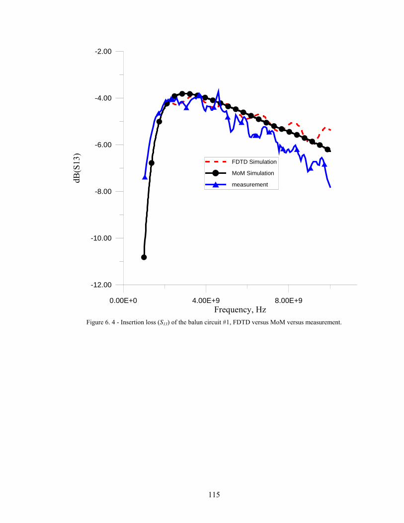
115
0.00E+0 4.00E+9 8.00E+9Frequency, Hz
-12.00
-10.00
-8.00
-6.00
-4.00
-2.00
dB(S
13)
FDTD Simulation
MoM Simulation
measurement
Figure 6. 4 - Insertion loss (S13) of the balun circuit #1, FDTD versus MoM versus measurement.

116
0.00E+0 4.00E+9 8.00E+9Frequency, Hz
-200.00
-100.00
0.00
100.00
200.00
Phas
e(S1
3)FDTD Simulation
Measurement
MoM Simulation
Figure 6. 5 - Insertion loss Phase(S13) of the balun circuit #1, FDTD versus MoM versus measurement.

117
Summary
A full-wave FDTD and MoM have been used to analyze the multilayer spiral
transmission-line balun; the results obtained were compared to the result obtained from
the four-port measurements. In all cases the output matched reasonably well. The
difference between Empire (FDTD) and Momentum (MoM) were compared, every
software has it is own advantages and disadvantages. The geometrical dimension of the
balun under comparison was presented in Appendix A (balun number 1).
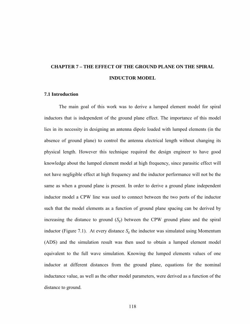
118
CHAPTER 7 – THE EFFECT OF THE GROUND PLANE ON THE SPIRAL
INDUCTOR MODEL
7.1 Introduction
The main goal of this work was to derive a lumped element model for spiral
inductors that is independent of the ground plane effect. The importance of this model
lies in its necessity in designing an antenna dipole loaded with lumped elements (in the
absence of ground plane) to control the antenna electrical length without changing its
physical length. However this technique required the design engineer to have good
knowledge about the lumped element model at high frequency, since parasitic effect will
not have negligible effect at high frequency and the inductor performance will not be the
same as when a ground plane is present. In order to derive a ground plane independent
inductor model a CPW line was used to connect between the two ports of the inductor
such that the model elements as a function of ground plane spacing can be derived by
increasing the distance to ground (Sg) between the CPW ground plane and the spiral
inductor (Figure 7.1). At every distance Sg the inductor was simulated using Momentum
(ADS) and the simulation result was then used to obtain a lumped element model
equivalent to the full wave simulation. Knowing the lumped elements values of one
inductor at different distances from the ground plane, equations for the nominal
inductance value, as well as the other model parameters, were derived as a function of the
distance to ground.
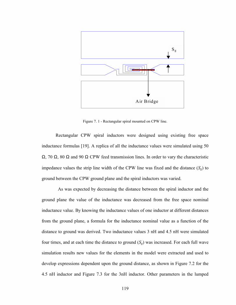
119
Sg
Air Bridge
Figure 7. 1 - Rectangular spiral mounted on CPW line.
Rectangular CPW spiral inductors were designed using existing free space
inductance formulas [19]. A replica of all the inductance values were simulated using 50
Ω, 70 Ω, 80 Ω and 90 Ω CPW feed transmission lines. In order to vary the characteristic
impedance values the strip line width of the CPW line was fixed and the distance (Sg) to
ground between the CPW ground plane and the spiral inductors was varied.
As was expected by decreasing the distance between the spiral inductor and the
ground plane the value of the inductance was decreased from the free space nominal
inductance value. By knowing the inductance values of one inductor at different distances
from the ground plane, a formula for the inductance nominal value as a function of the
distance to ground was derived. Two inductance values 3 nH and 4.5 nH were simulated
four times, and at each time the distance to ground (Sg) was increased. For each full wave
simulation results new values for the elements in the model were extracted and used to
develop expressions dependent upon the ground distance, as shown in Figure 7.2 for the
4.5 nH inductor and Figure 7.3 for the 3nH inductor. Other parameters in the lumped

120
element model were also affected by varying the distance to ground, such as the mutual
capacitance between the spiral turns, and the capacitance between the ground plane and
the spiral turns (which should approach zero at infinite distance to ground), (Figures 7.4
to 7.7).
0.00 0.40 0.80 1.20 1.60 2.00Distance (mm)
2.80
3.20
3.60
4.00
4.40
Indu
ctan
ce (n
H)
Figure 7. 2 - Inductance versus ground plane distance for the 4.5nH inductor xeL 6.249.1
41.4−+
= .

121
0.00 0.40 0.80 1.20 1.60 2.00Distance (mm)
2.00
2.20
2.40
2.60
2.80
3.00
Indu
ctan
ce (n
H)
Figure 7. 3 - Inductance versus ground plane distance for the 3nH Inductor xeL 2.1043.1
9.2−+
= .

122
0.00 0.40 0.80 1.20 1.60 2.00Distance (mm)
0.00
0.04
0.08
0.12
0.16
0.20
Cap
acita
nce
(pF)
Figure 7. 4 – Capacitance to ground versus ground plane distance for the 4.5nH inductor
xg eC 208.2771.1
033.0−−
= .

123
0.00 0.40 0.80 1.20 1.60 2.00Distance (mm)
0.00
0.04
0.08
0.12
0.16
Cap
acita
nce
(pF)
Figure 7. 5 – Capacitance to ground versus ground plane distance for the 3nH inductor
xg eC 077.981.1
00311.0−−
= .
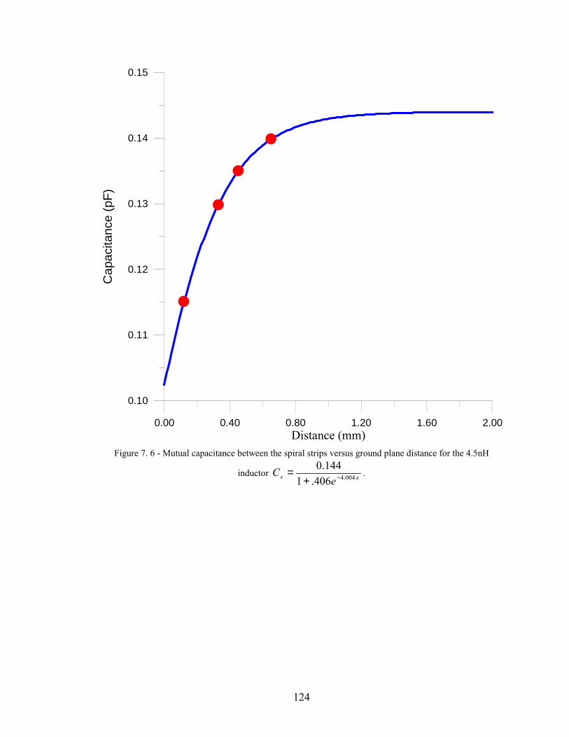
124
0.00 0.40 0.80 1.20 1.60 2.00Distance (mm)
0.10
0.11
0.12
0.13
0.14
0.15
Cap
acita
nce
(pF)
Figure 7. 6 - Mutual capacitance between the spiral strips versus ground plane distance for the 4.5nH
inductor xs eC 004.4406.1
144.0−+
= .

125
0.00 0.40 0.80 1.20 1.60 2.00Distance (mm)
0.11
0.12
0.13
0.14
0.15
Cap
acita
nce
(pF)
Figure 7. 7 - Mutual capacitance between the spiral strips versus ground plane distance for the 3nH
inductor xs eC 201.2291.1
148.0−+
= .

126
It should be mentioned that square and circular spiral inductors are more practical
than the rectangular shape spiral inductors since they exhibit a higher Q-factor and higher
resonant frequency. However, the rectangular geometry is more convenient in this
research for studying the effect of ground spacing since for certain characteristic
impedance the distance to ground is fixed and to get different inductance values all that
has to be changed is the length of the spiral inductor.
127
7.2 Spiral Inductor
The CPW spiral inductor modeled here is shown in Figure 7.8. It should be noted
that the spiral under consideration is a rectangular one of width do1 and length do2. An air-
bridge is used to connect the inner port of the spiral to the output CPW (Figure 7.1). The
number of turns (N) is two. Only the length of the spiral (do2) was varied to vary the
inductance value.
W
do2
do1
S
bb di2
b
b
di2
Figure 7. 8 - Two-turn rectangular spiral inductor.

128
When analyzing a CPW rectangular spiral inductor the following parameters need to
be specified:
1. do1: the outer width of the spiral.
2. do2: the outer length of the spiral.
3. W: the spiral strip width.
4. S: the spacing between the spiral turns.
5. Sg: the distance between the outermost turn and the ground plane (Ground
spacing).
6. Ha: the height of the air-bridge.
7. Wa: the width of the air-bridge.
8. t: the metallization thickness.
9. ρ: The metallization resistivity.
After a thorough literature search and numerical experiments, the lumped element
equivalent circuit shown in Figure 7.9 was chosen to model the CPW spiral inductor
[20]. This circuit should be applicable up to the first resonant frequency of the
inductor, which is the frequency range of interest as it represents the region where the
spiral acts as an inductor.

129
Figure 7. 9 - Spiral Inductor’s Lumped Element Model.
The optimized lumped elements nominal values should be converged to the
values obtained from the free space analytical formulas listed bellow when increasing
the value of the distance to ground (Sg). The values obtained using the analytical
formula can also be used to set the range by which the lumped element values will be
varied in the optimizer. The lumped element values of the spiral inductor model are
obtained as follows:
1- To evaluate the inductance L in free space, the simpler expression in [19] was
used.
+++
+−
++•+
++=
11
1
21
2
21
1
2
1
211
2
477.0
22
)))((
2ln()
))((2
ln(104
mm
m
mm
m
mm
m
m
m
mmm
dtbd
gd
ddtbgd
dddd
tbgddd
dNL
Where,
.
Port Port
frequencybafR +=)(
CS
Cg Cg
L Air-BridgeL

130
bddbddbddbddddg
waNbswa
im
im
mo
mo
mm
+=+=+=+=+=
+−=+=
22
11
22
11
22
21
)1(
With L in nH and all dimension in mm.
2- The resistance R was computed using the expression from [20], which takes the
skin effect into account: fbafR ∗+=)( , (where f is the frequency). The values
of the variables a and b were extracted from the EM full wave simulation result
(obtained from ADS- Momentum) through circuit optimization.
3- The series capacitor Cs models the parasitic capacitive coupling between the
input and the output ports of the inductor, as well as the turn-to-turn capacitance
in the spiral itself. Both the crosstalk between the adjacent turns and the overlap
between the spiral and air-bridge contribute to this capacitance Cs. The following
approximate expression is used to evaluate this capacitance:
bridgeaircouplings CCC −+= , where bridgeairC − is approximated as a parallel-plate
capacitance between the air-bridge and the spiral metallization. This
approximation is valid since the height of the air bridge is very small compared to
the bridge width and the spiral strip width.
a
aobridgeair H
WWNC ε=−
))()()()(1(21'212 kK
kKddN
NC mmroCoupling ++∗−= εε

131
2
))(4
tan(
=awk π , 2' 1 kk −=
Where )(kK and )( 'kK are the complete elliptic integral of the first kind of k and
k’, rε is the relative dielectric constant of the substrate. [19]
4- The parallel capacitors Cg is used to model the capacitance between the spiral
(mainly the outermost turn) and the ground plane. Usually the distance to the
ground Sg is large to reduce its effect on the spiral response. The expression for Cg
can be determined by considering every turn of the spiral as an asymmetric CPW
transmission line with line width equal to W [21], Cg is the sum of the individual
self capacitances of all the turns since these capacitance are connected in parallel.
5- LAir-Bridge can be evaluated if we consider the air bridge as a strip conductor in free
space. Since the air bridge strip width is small and relatively far from the ground
plane its inductance value can be assumed to be constant even with varying the
distance to ground. Using a free space closed-form expression for the strip
conductor in free space [24] the inductance of the air-bridge (Figure 7.10) can be
found as following: ]02235.193.1)[ln(102)( 4
ltw
twllnHL +∗+++
∗∗×= −
For a strip line of width 100µm, length 700µm and 3µm thickness the inductance
is equal 0.44 nH.
l
tW
Figure 7. 10 - Strip conductor in free space. l = length, w = width and t = thickness.

132
7.3 Lumped Element Model
Two spiral inductors 3nH and 4.5nH fed with 50Ω, 70Ω, 80Ω and 90Ω CPW
transmission lines were designed and simulated. The simulated results were then
optimized to extract the lumped element values in the equivalent circuit model as a
function of the characteristic impedance (distance to ground) as shown in Figure 7.11.
.
TermTerm2
Z=50 OhmNum=2
S_ParamSP1
Step=Stop=10 GHzStart=50 MHz
S-PARAMETERS
OptimOptim1
OPTIM
TermTerm3
Z=50 OhmNum=3
TermTerm4
Z=50 OhmNum=4Shem_CPW_70_5nH
X14
TermTerm1
Z=50 OhmNum=1 Data_CPW_70ohm_5nH
X13
GoalOptimGoal2Expr="mag(S21-S43)"SimInstanceName="SP1"Min=0Max=0.001Weight=1RangeVar[1]=RangeMin[1]=RangeMax[1]=
GOAL
GoalOptimGoal1Expr="mag(S11-S33)"SimInstanceName="SP1"Min=0Max=0.001Weight=1RangeVar[1]=RangeMin[1]=RangeMax[1]=
GOAL
Figure 7. 11 - Schematic diagram showing the optimization of the lumped element model and the data obtained from full wave simulation (Momentum - ADS).

133
Figure 7.12 shows the schematic diagram of the lumped element model and Figure 7.13
shows the schematic diagram of the simulated data blocks. Notice that the left and the
right taper, used to connect between the spiral inductor and the CPW line from both side,
were de-embedded to get correct optimized values. Figure 7.14 shows a drawing of a
4.5nH CPW spiral inductor and the location of the tapered-line sections. Figure 7.15 and
7.16 show comparisons between the insertion loss (IL) and the return loss (RL) of both
the full-wave EM simulation data and the result of the optimized equivalent circuit
model.
.
LL2R=
CC4
CC3
LL1R=
Z1P_EqnZ1P1Z[1,1]=complex(a+b*sqrt(freq),0)
CC1
VARVAR1
b=-6.45686e-06 opt -8 to 5 a=3.24818e-08 opt 0 to 5 L1=4.595 opt 2.5 to 6 C3=0.0431195 opt 0 to 2 C2=0.0785383 opt 0 to 2 L2=1.34825 opt 0 to 2 C1=0.131282 opt 0 to 2
EqnVar
PortP2Num=2
PortP1Num=1
Figure 7. 12 - Schematic diagram of the 4.5nH spiral lumped elements model.

134
.
Deembed2SNP3
21
Ref
S2PSNP1
21
Ref
Deembed2SNP2
21
Ref
PortP1Num=1
PortP2Num=2
Figure 7. 13 - Schematic diagram of the 4.5nH spiral data blocks with two de-embed blocks to cancel the
effect of the right and the left taper.
L e f t T a p e r R i g h t T a p e r
Figure 7. 14 - CPW spiral inductor, notice the left and right taper.

135
Due to a miscommunication with the company that was contracted to manufacture
the spiral inductors, the circuits were not properly fabricated. As such, only the full-wave
simulation data and the associated equivalent circuit model results are shown herein.
Actual performance should be very close to the simulated result due to the simplicity of
the structure.
0.00E+0 4.00E+9 8.00E+9Frequency, Hz
-50.00
-40.00
-30.00
-20.00
-10.00
0.00
dB(S
12)
Simulated Data
Optimized Data
Figure 7. 15 - Comparison of the insertion loss (S12) between the simulated data and the optimized circuit
model for the 4.5 nH inductor operated in 50Ω CPW line..

136
0.00E+0 4.00E+9 8.00E+9Frequency, Hz
-20.00
-15.00
-10.00
-5.00
0.00
5.00
dB(S
11)
Simulated Data
Optimized Data
Figure 7. 16 - Comparison of the return loss (S11) between the simulated data and the optimized circuit
model for the 4.5 nH inductor operated in 50Ω CPW line.

137
Summary
The elements in the lumped elements model of a spiral inductor have been
discussed and their nominal formulas have been presented. A lumped element model
that is independent of the ground plane has been derived for different spiral inductor
values. Formulas for the nominal inductance value, calculated in free space, as a
function of distance to ground in CPW line were also derived. Since the existing
inductor formulas for rectangular spiral inductors that can be found in literature
assume a free space condition, we have derived a formula that can be used to obtain
the value of the nominal inductance in the presence of the CPW ground plane. The
formula is a function of the distance to ground plane from the spiral inductor edge.
Furthermore formulas for the mutual capacitance between the spiral strips and for the
capacitance to ground of the spiral inductor were derived as a function of distance to
ground in CPW line.

138
CHAPTER 8 – CONCLUSIONS AND RECOMMENDATIONS
8.1 Conclusion
In this work we derived a design procedure to help RF engineers design cost
effective multilayer CPW spiral balun that works in the frequency range 1-8 GHz.
Furthermore three techniques to enhance the balun performance were developed. The
importance of the balun for feeding symmetric resonant antenna dipole was discussed, in
addition to the balun background and its impedance analysis. The accuracy of the
developed procedure has been proven by designing two balun circuits of different
dimensions and simulating them using available commercial software, Momentum
(MoM) and Empire (FDTD). The simulation results have shown good balun performance
over the desired frequency range. It has been also shown through this work that
introducing some capacitance at certain points in the balun circuit decreases both the
phase difference and the amplitude imbalance of the balun. Furthermore some of the
designed balun circuits have been fabricated and measured and the results agreed with the
simulations.
A procedure to derive independent of ground lumped element model, which is
independent of ground for spiral inductor, has been discussed at the end of this work.
Formulas for lumped elements in the spiral inductors model were extracting as a function
of distance to ground. The result showed that the nominal inductance value in the
inductor model decreased by reducing the distance to ground (slot width in the

139
CPW line) and the capacitance to ground decreased by increasing the CPW line slot
width.
8.2 Recommendations
Using the two derived lumped element models for the balun circuit, further work
in future can be done to study the effect of varying physical parameter values in the
balun circuit on the balun performance. More detailed analysis can be performed on
the derived compensation techniques to understand its operation. The derived
independent of ground lumped element model of the spiral inductor can be tested in
the design of an antenna dipole loaded with spiral inductor.

140
REFERENCES
[1] Inder Bahl, “RF and Microwave Coupled Line circuit”.
[2] Nathan Marchand “Transmission-line conversion,” Federal Telephone and Radio Laboratories New York, N. Y.
[3] Roperts, “A new Wide-Band Balun”.
[4] S.L. March, “Phase velocity Compensation in paralle coupled Microsrtip,” IEEE-MTT-S Int. Microwave Symp. Dig. , pp 410-412, 1982.
[5] G. Schaller, “Optimization of Microstrip Directional couplers with Lumped Capacitors,” Arch Elel. Uebertage. Tech., vol. 31, pp 301-307, Jul-Aug. 1977.
[6] Ng, C.Y.; Chongcheawchamnan, M.; Robertson, I.D, “Analysis and design of a high-performance planar Marchand balun”. Microwave Symposium Digest, 2002 IEEE MTT-S International , 2002 Page(s): 113 -116 vol.1.
[7] K.; Toyoda, I.; Tokumitsu, T., “Compact and broad-band three-dimensional MMIC balun Nishikawa” Microwave Theory and Techniques, IEEE Transactionson, Volume: 47Issue:1, Jan.1999 Page(s): 96 –98.
[8] Shimozawa, M.; Itoh, K.; Sasaki, Y.; Kawano, H.; Isota, Y.; Ishida, O., “A parallel connected Marchand balun using spiral shaped equal length coupled lines” Microwave Symposium Digest, 1999 IEEE MTT-S International , Volume: 4 , 1999 Page(s): 1737 -1740 vol.4.
[9] Kian Sen Ang; Robertson, I.D., “Analysis and design of impedance-transforming planar Marchand baluns” Microwave Theory and Techniques, IEEE Transactions on , Volume: 49 Issue: 2 , Feb. 2001 Page(s): 402 –406.

141
[10]Yeong J. Yoon, Yicheng Lu, Member, IEEE, Robert C. Frye, Member, IEEE, Maureen Y. Lau,Peter R. Smith, Lou Ahlquist, and Dean P. Kossives, “Design and Characterization of Multilayer Spiral Transmission-Line Baluns”.
[11] Yeong J,Yoon Member IEEE, Robert C. Frye, member IEEE, “A silicon Monolithic Spiral Transmission Line Balun with Symmetrical design”.
[12] Nishikawa, K.; Toyoda, I.; Tokumitsu, T., “Compact and broad-band three-dimensional MMIC balun” Microwave Theory and Techniques, IEEE Transaction son, Volume: 47Issue:1, Jan.1999 Page(s): 96 –98.
[13] T. Itoh, Numerical Techniques for Microwave and Millimeter-Wave Passive Structures. New York: J. Wiley, 1989.
[14] J. J. H. Wang, Generalized Moment Methods in Electromagnetics; Formulation and Computer Solution of Integral Equations. New York. J. Wiley, 1991. [15] M. Sadiku, Numerical Techniques in Electromagnetics. Boca Raton, FL. CRC Press, 1992.
[16] K. S. Yce " Numerical Solution of iniria1 boundary value problem in solving Maxwell's equations in isotropic media," IEEE Trans, Antennas Propagation, vol. AP-14, pp, 302-307, May 1966.
[17] G. Mur, "Absorbing boundary conditions for the finite difference approximation of the time-domain electromagneric field equations," IEEE Trans. Electromagn. Compat., vol. 23, pp. 377-382, Nov 1981.
[18] J J. P. Berenger, "A perfectJy matched layer for the absorption of electromagnetics waves," J. Computational Phys., vol. 114, pp. 185-200, 1994.
[19] T. Koryu Ishii, Handbook of Microwave Technology, New York, Academic Press, 1995.
[20] M. Abdo-Tuko, M. Naghed, and I. Wolff, ”Novel 18/36 GHz (M) MIC GaAs FET Frequency Doublers”

142
[21] Brian C. Wadell, “Transmission Line Design Handbook”, Artech House, 1991.

143
APPENDICES

144
APPENDIX A - BALUN GEOMETRICAL DIMENSIONS
Table A. 1 - Common geometrical dimension of the small size balun. See (Figure 3.22 – Figure 3.24) in section 3.4 for parameters visualization.
Spiral strip line width 25µm
Spiral gap width 25µm
Spiral inner radius 212µm
Spiral outer radius 338µm
Horizontal offset 10µm
Vertical offset (polyimide 1 thickness) 10µm
Polyimide 2 thickness 10µm
Polyimide 1 and 2 permittivity 2.6
Quartz permittivity 3.8
Quartz thickness 25 mil
Spiral line width 6.7 mm
CPW line width 0.21 mm
CPW line slot width .03 mm

145
APPENDIX A (Continued)
Figure A. 1 Balun number 1, dimensions are in mm.

146
APPENDIX A (Continued)
Figure A. 2 Balun number 2, dimensions are in mm.

147
APPENDIX A (Continued)
Figure A. 3 Balun number 3, dimensions are in mm.
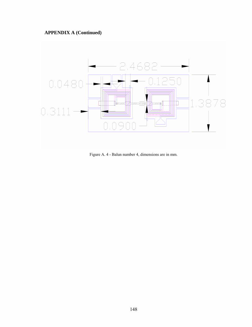
148
APPENDIX A (Continued)
Figure A. 4 - Balun number 4, dimensions are in mm.

149
APPENDIX B – FOUR-PORT ON-WAFER TRL CALIBRATION AND BALUN
MEASUREMENT PROCEDURE
B.1 Equipments Configuration
The four-port on-wafer TRL calibration and the balun measurements were performed
using the following equipments:
• Anristu Lightening Network Analyzer • Flexible Coaxial Cables (4) • SUSS Semi-automatic Probing Station • PC with a GPIB Port • GPIB Cable (1) • NIST-Cal (Multi-Port NIST) Installed on PC • 2-Port to 4-Port Switch Box (1) • Semi-flex Coaxial Cables with K connectors (2) • CGB Wafer Pico-probes (4) • 6 GHz Balun Wafer fabricated by ATC • SMA to K connector (2) • TRL Calibration Substrate (1)
Figure B. 1 - General equipment configuration for the measurement.

150
Appendix B (Continued)
B.2 Calibration Kit
The Coplanar Waveguide width dimensions for the small size balun measurements are as follows:
1. Signal Line width 0.21 mm 2. Gap width 30um
Figure B. 2 – CPW calibration kit dimension.
The Cal kit consists of the following standards:
1. Thru line connection with a length of 0.4mm (thru =0.2mm) 2. 2 delay line lines:
a. At 4GHz with a length of 12.5mm. b. At 6GHz with a length of 8.5mm.
3. Open standard with a pad length of 0.2mm.
B.3 Calibration Setup
Before starting the Multi-Port NIST program, it is important to set up a number of
folders for the data to be stored. We will need one folder for calibration standards, and
one folder for every Balun that will be measured. It is also important to go ahead and set
up the VNA to default specifications. This needs to be done before proceeding to the
following steps.
1. Open the NIST Multi-port Calibration Software.

151
2. Click on 8510 Tab from main menu and change the selection to Anritsu
Lightening
3. Click on Error Box Configuration from main menu and make sure all ports are
transparent.
4. Click on the Perform 4 Port Calibration tab from main menu
5. Click on Measure and then go to Browse Cal.
6. Open the folder that we have designated as our calibration data folder and click on
the Select Current Directory.
7. Click on Browse Device and open the folder we’ve designated as the Balun
folder. Click on Select Current Directory. This folder should be the Balun we are
measuring first.
Now enter the names of our cal standards, i.e. thru, line, open/ short.
The name that entered does not matter, but where we put that name does matter.
All these files will be stored in the calibration directory we have selected.
Note: make sure the GPIB address field is set to 16.
8. For the line standard enter a name in the 1st row to the right of the Start tab, select
a name such as delay1SB. This will make locating the file easier. If there are
multiple delay lines, enter it to into the next row under the 1st line. Make sure a
different name is given.
9. For the reflect standard, enter a name in any of the remaining rows except the thru
row. Once a name is assigned, click on the reflect dot to the left of the reflect
name. It does not matter if we have entered and open or a short name.
10. Finally, enter a name for the thru standard in the standard row.

152
Setting up the file names is now completed. It is time to make calibration
measurements. There is no need at this point to define calibration standard. This is taken
care of in the later steps.
B.4 Calibration Measurement
1. Make sure that the tab at the top of the measure window is set at the measure
West/East Calibration STD’s.
2. Connect the line standard to the west and east ports, and click the start tab
corresponding to the line standard. Wait until measurement is through. The
measurement was done with “probe-tip” calibration reference planes, since in the
calibration the reference was not at zero but it was shifted to the outside of the
circuit by 0.185mm.
Figure B. 3 - Insertion loss- S21- for delay line at 6GHz (West-East).

153
Figure B. 4 - Return loss - S11 - for delay line at 6GHz (West-East).
Figure B. 5 - Insertion loss - S21- for delay line at 8GHz (West-East).

154
Figure B. 6 - Return loss- S11- for delay line at 8GHz (West-East).
3. Connect the open standard and click the corresponding tab. if the reflect
measurement is made using only one port at a time then click the 2-P tab before
starting the measurements.

155
Figure B. 7 - Insertion loss- S21- for Open (West-East).
Figure B. 8 - Return loss- S11- for open (West-East). Notice that the decay in phase is due to the amount of
calibration reference shift

156
4. Continue to the thru standard.
Figure B. 9 - Insertion Loss- S21 - for Thru (North-South).
Figure B. 10 - Return loss- S11- for Thru (North-South).
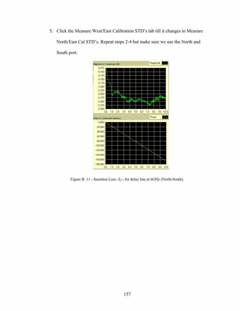
157
5. Click the Measure West/East Calibration STD’s tab till it changes to Measure
North/East Cal STD’s. Repeat steps 2-4 but make sure we use the North and
South port.
Figure B. 11 - Insertion Loss- S21- for delay line at 6GHz (North-South).

158
Figure B. 12 - Return loss- S11 - for delay line at 6GHz (North-South).
Figure B. 13 - Return loss- S11 - for delay line at 6GHz (South - North).

159
Figure B. 14 - Return loss- S11- for delay line at 8GHz (South-North)
6. Click continue. This concludes the measurements of our cal standards.

160
B.5 Calculating Correction Factor
1. Click on Calibrate West/East tab. We should see all the line standards that we
have measured in the menus, but without line
2. Lengths. Enter the physical line lengths at this time.
Figure B. 15 - Menu display for calculating Calibration Coefficients and Error Boxes.
3. The software has a reflect standard defaulted as a short. Change to an open and
record the reflect length.
4. Enter the estimated dielectric constant (Er=2.25).
5. When done recording values, click on Calculate Calibration Coefficients and
Error Boxes.
6. Click Display Corrected Data.
7. Look thru this thoroughly to check for good calibration. If the calibration is bad,
repeat the calibration steps. There is no need to repeat the Balun measurement.
8. Click Continue to exit out of window.

161
9. Save the corrected data. Saving the corrected data might take a few minutes
depending on the PC.
10. Repeat steps 1-9 for the North/South, and South/North configurations.
B.6 Making The Four-Port Measurement
1. In the measurement setup window verify the selection of measuring single ended
S-parameters and not the differential S-parameters
2. From Four Port main menu, click Measure.
3. Change the device path for which you want the Balun to be located.
4. Attach the Balun to the ports making note which measurement port is attached to
which device port. Make sure you are extremely careful when landing the probes
on the wafer. Stop the descending of the probes after a maximum of 30micron of
skating. Click Measure 4-Port. When lifting the probes observe the skating marks
on the metal and make sure all probe tips contacted properly with the circuit.
5. Repeat steps 2-3 making sure we change the dive path.
B.6 De-embedding The Four-Port Measurement
1. Go to Measure from the 4-port main menu and change the device path to the one
our Balun is currently located.
2. Repeat the steps in the section Calculating Correction Coefficients. This step is so
that our calibration coefficients are placed in the device directory for de-
embedding. When saving the coefficients in these steps, replace any files when
prompted to.
3. From the main menu click on 4-Por Calibrate.

162
4. Click De-embed Four Port from the 4-port main menu.
5. Make sure that the device directory is set to the Balun that we have measured.
Also make note of the port definitions. We will use this when looking at our data.
6. If using ADS for the s4p data, change the format to Touchtone
7. If we want to look at the data in the NIST program, we will have to de-embed the
device in Column (dB-phase) format. The NIST program will only read Column
(dB-phase).
8. Click De-embed and save Four Prot S-Parameters.
9. Click Exit when finished.
B.7 Display corrected Four-Port Data
1. From 4-port main menu, click Display corrected 4-port data.
2. Choose the text file in which we named previously for the device.