Embed Size (px)
Citation preview
Design and Analysis of High‐Speed Links
1
Wendem BeyeneRambus Inc. Sunnyvale, CA USA
17th Workshop onSignal and Power Integrity (SPI)
May 12‐15, 2013Paris, France
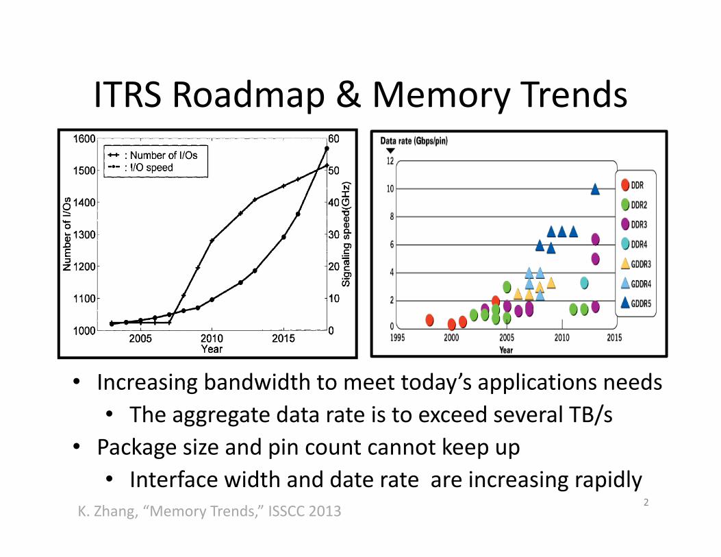
ITRS Roadmap & Memory Trends
• Increasing bandwidth to meet today’s applications needs• The aggregate data rate is to exceed several TB/s
• Package size and pin count cannot keep up • Interface width and date rate are increasing rapidly
2K. Zhang, “Memory Trends,” ISSCC 2013
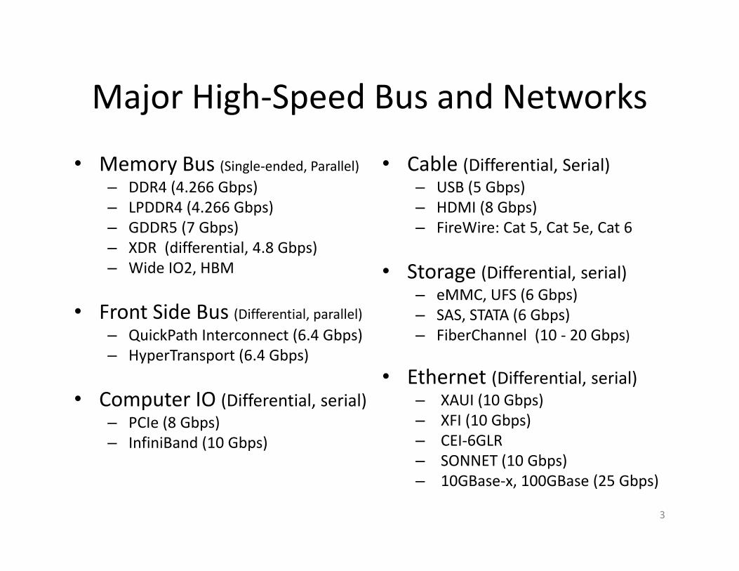
Major High‐Speed Bus and Networks
• Memory Bus (Single‐ended, Parallel)– DDR4 (4.266 Gbps)– LPDDR4 (4.266 Gbps)– GDDR5 (7 Gbps)– XDR (differential, 4.8 Gbps)– Wide IO2, HBM
• Front Side Bus (Differential, parallel)– QuickPath Interconnect (6.4 Gbps)– HyperTransport (6.4 Gbps)
• Computer IO (Differential, serial)– PCIe (8 Gbps)– InfiniBand (10 Gbps)
• Cable (Differential, Serial)– USB (5 Gbps)– HDMI (8 Gbps)– FireWire: Cat 5, Cat 5e, Cat 6
• Storage (Differential, serial)– eMMC, UFS (6 Gbps)– SAS, STATA (6 Gbps)– FiberChannel (10 ‐ 20 Gbps)
• Ethernet (Differential, serial)– XAUI (10 Gbps)– XFI (10 Gbps)– CEI‐6GLR– SONNET (10 Gbps)– 10GBase‐x, 100GBase (25 Gbps)
3
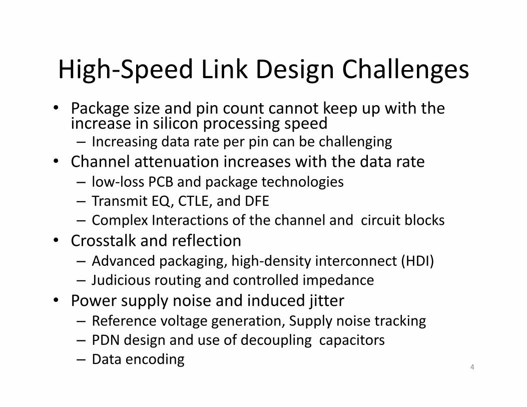
High‐Speed Link Design Challenges• Package size and pin count cannot keep up with the increase in silicon processing speed– Increasing data rate per pin can be challenging
• Channel attenuation increases with the data rate– low‐loss PCB and package technologies– Transmit EQ, CTLE, and DFE – Complex Interactions of the channel and circuit blocks
• Crosstalk and reflection – Advanced packaging, high‐density interconnect (HDI) – Judicious routing and controlled impedance
• Power supply noise and induced jitter– Reference voltage generation, Supply noise tracking– PDN design and use of decoupling capacitors– Data encoding
4
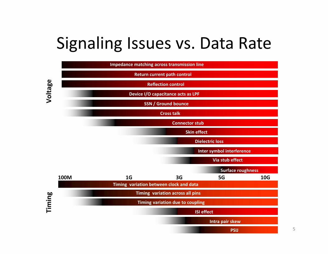
Signaling Issues vs. Data RateTiming Timing variation across all pins
Timing variation between clock and data
Timing variation due to coupling
PSIJ
Intra pair skew
ISI effect
Volta
ge
Return current path control
SSN / Ground bounce
Cross talk
Surface roughness
Connector stub
Impedance matching across transmission line
Reflection control
Device I/O capacitance acts as LPF
Via stub effect
Dielectric loss
Inter symbol interference
Skin effect
1G100M 3G 5G 10G
5
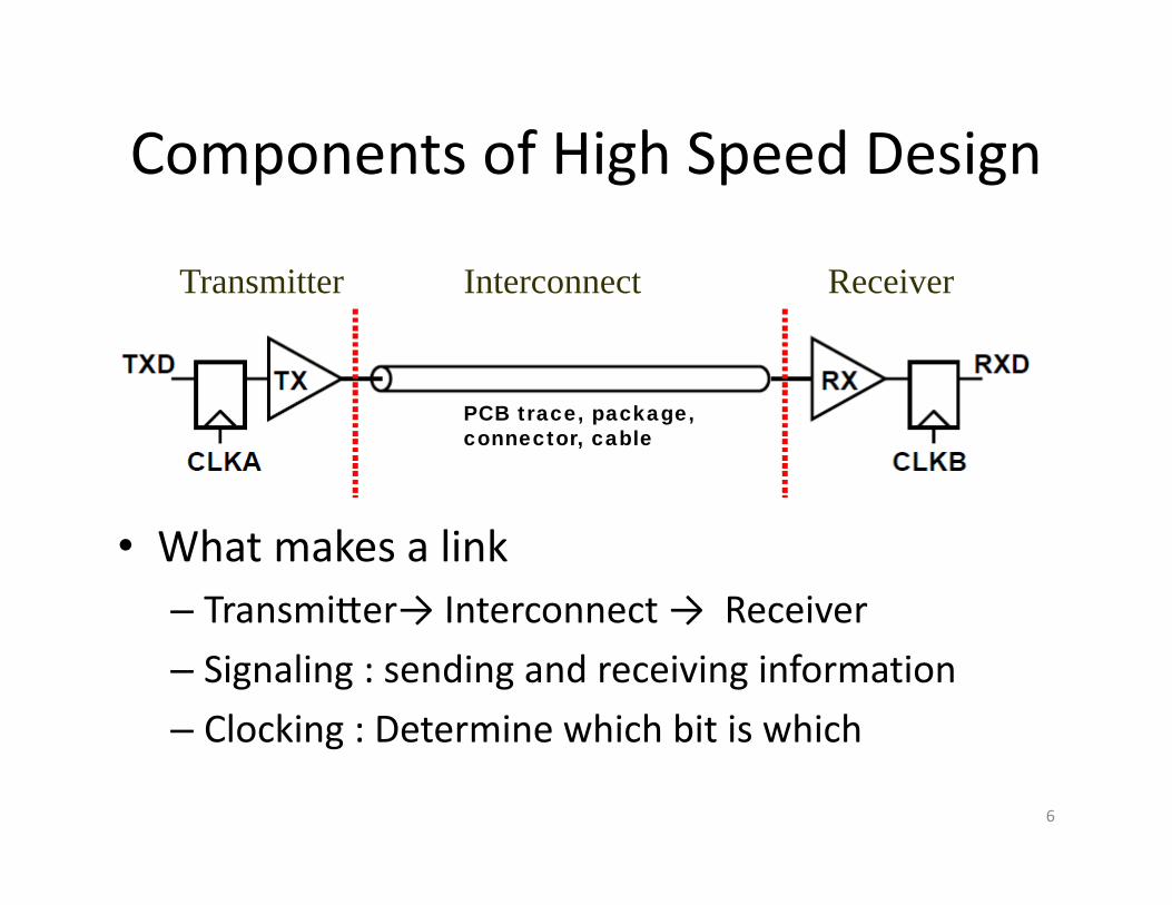
Components of High Speed Design
• What makes a link– Transmi er→ Interconnect → Receiver– Signaling : sending and receiving information– Clocking : Determine which bit is which
6
Transmitter Interconnect Receiver
PCB trace, package,connector, cable
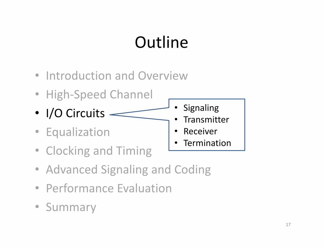
Outline
• Introduction and Overview• High‐Speed Channel• I/O Circuits• Equalization• Clocking and Timing • Advanced Signaling• Performance Evaluation• Summary
7
• Typical channels• Source of losses• Reflection • Crosstalk• ISI
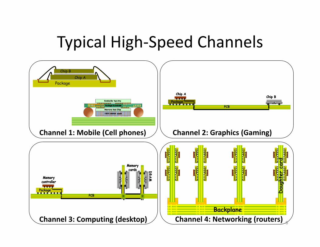
Typical High‐Speed Channels
Package
Memory controller
PCB
DRA
MMemory cards
Package
Memory controller
PCB
DRA
MMemory cards
PCBPCB
Chip BPackage
Chip A
PCBPCBPCB
Chip BPackage
Chip A
PCB
PackagePackage
PackagePackage
PackagePackage
PackagePackage
PackagePackage
PackagePackage
PackagePackage
PackagePackage
PackagePackage
PackagePackage
PackagePackage
PackagePackage
PackagePackage
PackagePackage
PackagePackage
PackagePackage
PackagePackage
PackagePackage
PackagePackage
PackagePackage
PackagePackage
PackagePackage
PackagePackage
PackagePackage
PackagePackage
PackagePackage
PackagePackage
PackagePackage
PackagePackage
PackagePackage
PackagePackage
PackagePackage
PackagePackage
PackagePackage
PackagePackage
PackagePackage
PackagePackage
PackagePackage
PackagePackage
PackagePackage
PackagePackage
PackagePackage
PackagePackage
PackagePackage
PackagePackage
PackagePackage
PackagePackage
PackagePackage
Backplane
Dau
ghte
r ca
rd
Channel 1: Mobile (Cell phones)
Channel 3: Computing (desktop) Channel 4: Networking (routers)
Channel 2: Graphics (Gaming)
PackageChip A
Chip B
8
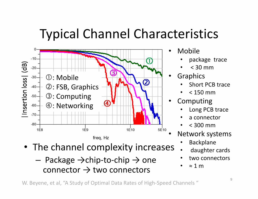
Typical Channel Characteristics
: Mobile: FSB, Graphics: Computing: Networking
• The channel complexity increases– Package →chip‐to‐chip → one connector → two connectors
9
• Mobile• package trace• < 30 mm
• Graphics• Short PCB trace • < 150 mm
• Computing• Long PCB trace• a connector• < 300 mm
• Network systems• Backplane • daughter cards• two connectors• ≈ 1 m
W. Beyene, et al, “A Study of Optimal Data Rates of High‐Speed Channels “
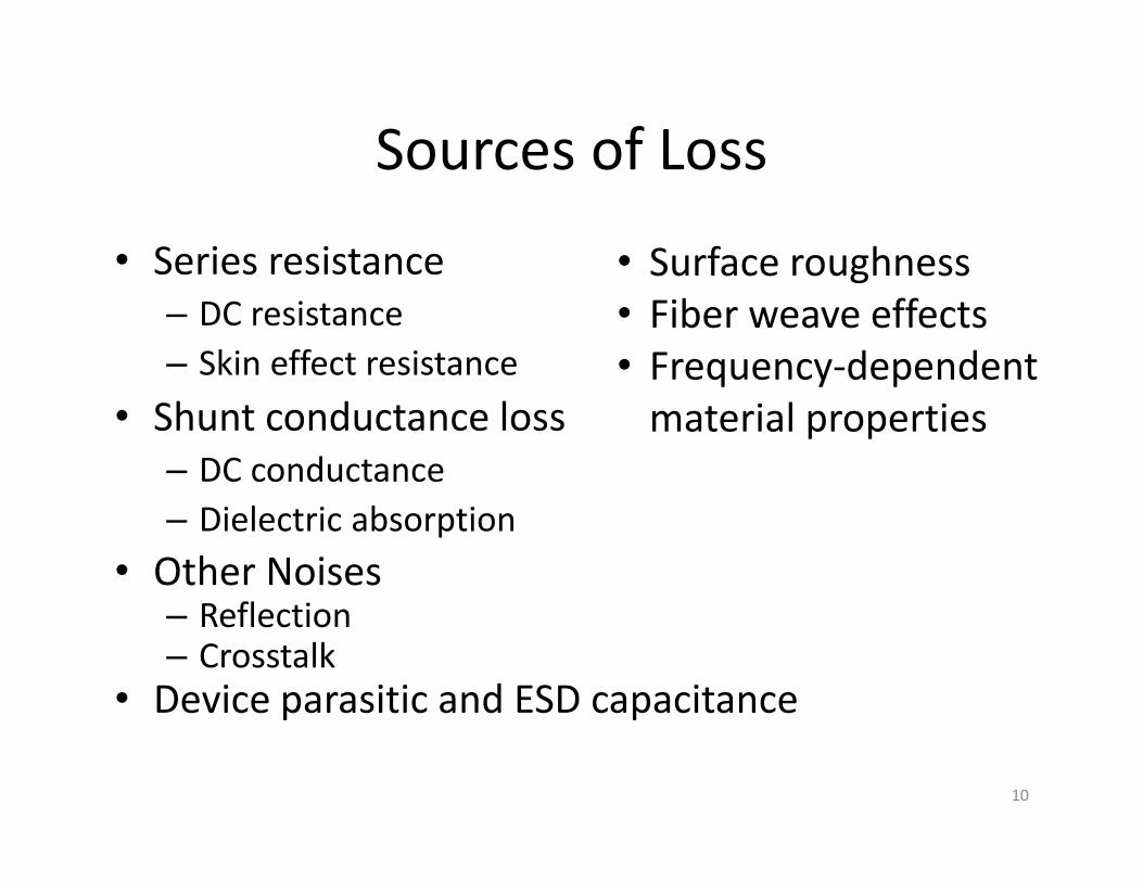
Sources of Loss
• Series resistance– DC resistance– Skin effect resistance
• Shunt conductance loss– DC conductance– Dielectric absorption
• Other Noises– Reflection – Crosstalk
• Device parasitic and ESD capacitance
10
• Surface roughness• Fiber weave effects• Frequency‐dependent material properties
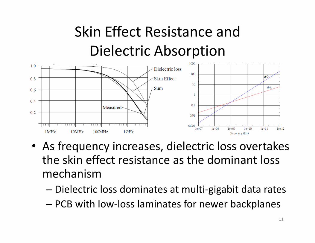
Skin Effect Resistance andDielectric Absorption
• As frequency increases, dielectric loss overtakes the skin effect resistance as the dominant loss mechanism– Dielectric loss dominates at multi‐gigabit data rates– PCB with low‐loss laminates for newer backplanes
11
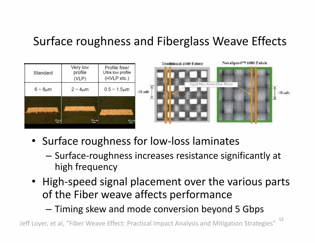
Surface roughness and Fiberglass Weave Effects
• Surface roughness for low‐loss laminates – Surface‐roughness increases resistance significantly at high frequency
• High‐speed signal placement over the various parts of the Fiber weave affects performance– Timing skew and mode conversion beyond 5 Gbps
12Jeff Loyer, et al, “Fiber Weave Effect: Practical Impact Analysis and Mitigation Strategies”
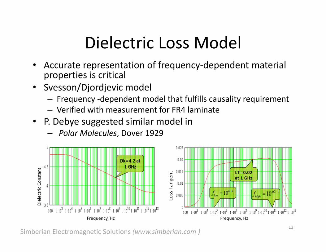
Dielectric Loss Model• Accurate representation of frequency‐dependent material
properties is critical• Svesson/Djordjevic model
– Frequency ‐dependent model that fulfills causality requirement– Verified with measurement for FR4 laminate
• P. Debye suggested similar model in– Polar Molecules, Dover 1929
Dielectric Con
stant
Frequency, Hz Frequency, Hz
Loss Tangent
13Simberian Electromagnetic Solutions (www.simberian.com )
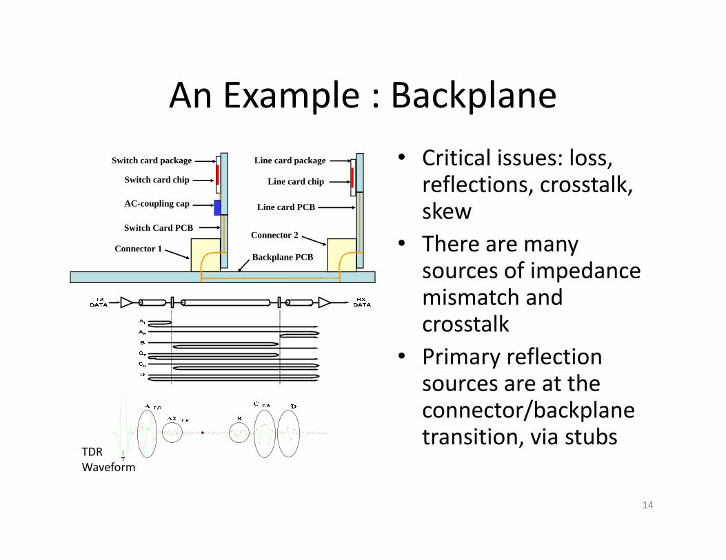
An Example : Backplane• Critical issues: loss, reflections, crosstalk, skew
• There are many sources of impedance mismatch and crosstalk
• Primary reflection sources are at the connector/backplane transition, via stubs
14
Connector 2Switch Card PCB
Line card package
Line card chip
Backplane PCB
AC-coupling cap Line card PCB
Connector 1
Switch card package
Switch card chip
TDRWaveform
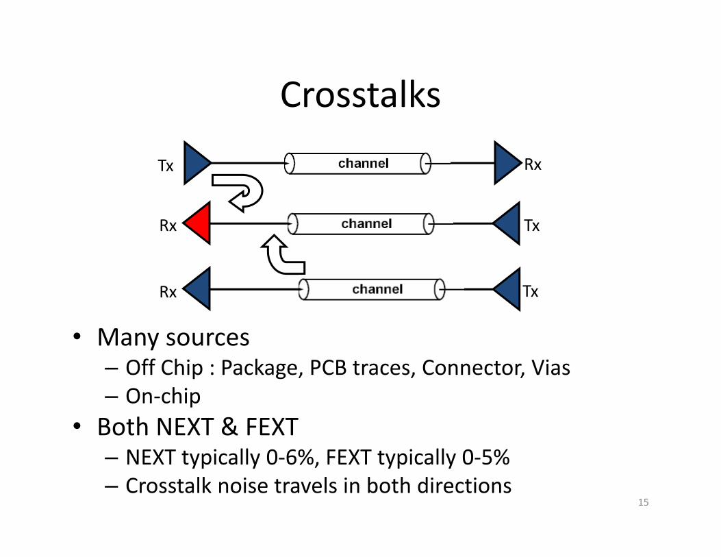
Crosstalks
• Many sources– Off Chip : Package, PCB traces, Connector, Vias– On‐chip
• Both NEXT & FEXT– NEXT typically 0‐6%, FEXT typically 0‐5%– Crosstalk noise travels in both directions
15
Tx
Tx
Tx Rx
Rx
Rx
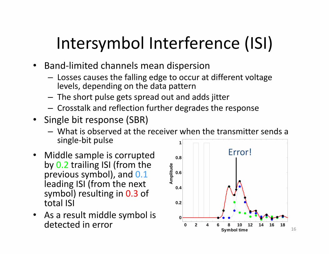
Intersymbol Interference (ISI)• Band‐limited channels mean dispersion
– Losses causes the falling edge to occur at different voltage levels, depending on the data pattern
– The short pulse gets spread out and adds jitter– Crosstalk and reflection further degrades the response
• Single bit response (SBR)– What is observed at the receiver when the transmitter sends a
single‐bit pulse
160 2 4 6 8 10 12 14 16 18
0
0.2
0.4
0.6
0.8
1
Symbol time
Am
plitu
de
Error!• Middle sample is corrupted by 0.2 trailing ISI (from the previous symbol), and 0.1leading ISI (from the next symbol) resulting in 0.3 of total ISI
• As a result middle symbol is detected in error
Outline
• Introduction and Overview• High‐Speed Channel• I/O Circuits• Equalization• Clocking and Timing • Advanced Signaling and Coding• Performance Evaluation• Summary
17
• Signaling• Transmitter• Receiver• Termination
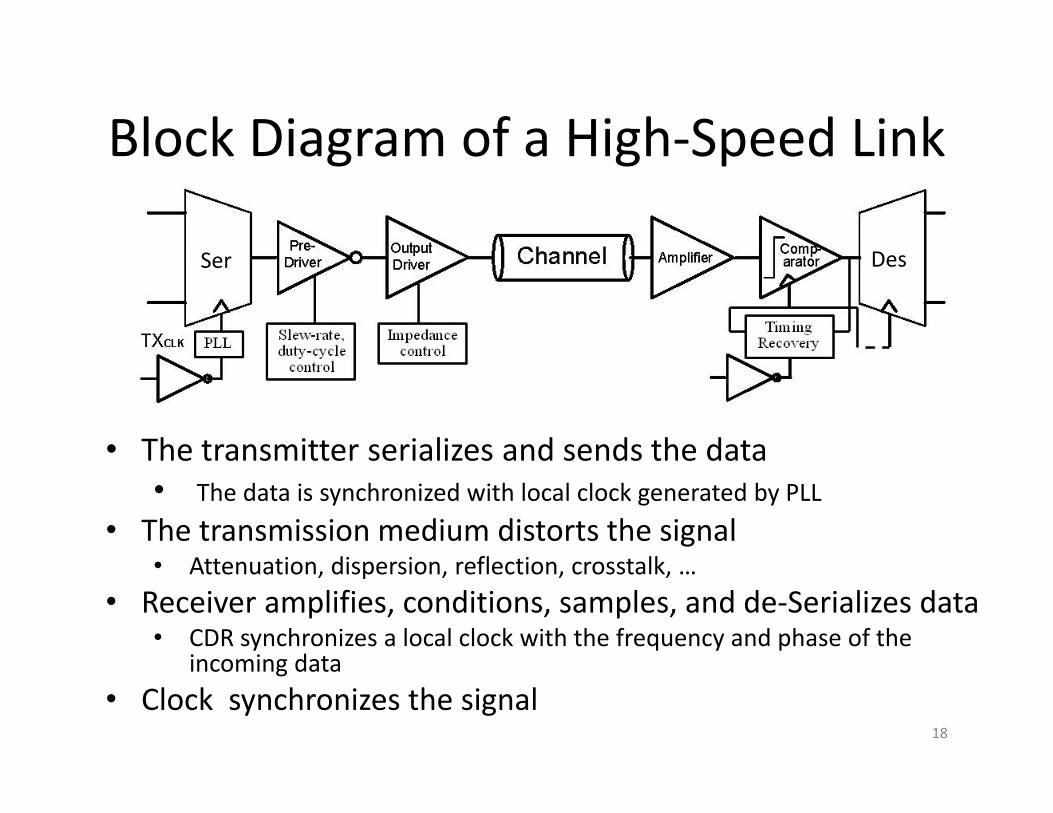
Block Diagram of a High‐Speed Link
18
• The transmitter serializes and sends the data• The data is synchronized with local clock generated by PLL
• The transmission medium distorts the signal• Attenuation, dispersion, reflection, crosstalk, …
• Receiver amplifies, conditions, samples, and de‐Serializes data • CDR synchronizes a local clock with the frequency and phase of the
incoming data • Clock synchronizes the signal
Ser Des
Single‐ended vs. Differential
• Single‐ended signaling – compare to shared reference– Often used with a bus
• Issues– Generates SSO noise– How to make reference– How to quiet reference : difference in bypass network if shared
– Crosstalk cannot be made common‐mode• Differential must run > 2x as fast as single‐ended to make sense– More expensive to implement ?
19

20
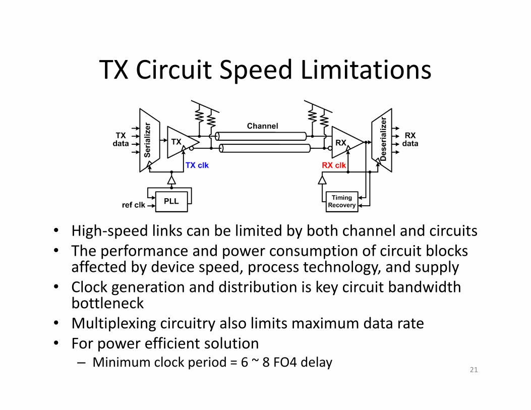
TX Circuit Speed Limitations
• High‐speed links can be limited by both channel and circuits• The performance and power consumption of circuit blocks
affected by device speed, process technology, and supply• Clock generation and distribution is key circuit bandwidth
bottleneck• Multiplexing circuitry also limits maximum data rate• For power efficient solution
– Minimum clock period = 6 ~ 8 FO4 delay21
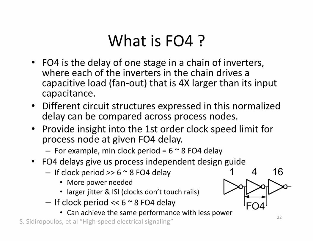
What is FO4 ?• FO4 is the delay of one stage in a chain of inverters, where each of the inverters in the chain drives a capacitive load (fan‐out) that is 4X larger than its input capacitance.
• Different circuit structures expressed in this normalized delay can be compared across process nodes.
• Provide insight into the 1st order clock speed limit for process node at given FO4 delay.– For example, min clock period = 6 ~ 8 FO4 delay
• FO4 delays give us process independent design guide– If clock period >> 6 ~ 8 FO4 delay
• More power needed• larger jitter & ISI (clocks don’t touch rails)
– If clock period << 6 ~ 8 FO4 delay • Can achieve the same performance with less power
1 4 16
FO422
S. Sidiropoulos, et al “High‐speed electrical signaling”
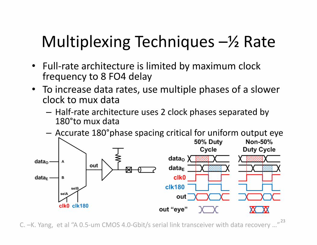
Multiplexing Techniques –½ Rate• Full‐rate architecture is limited by maximum clock frequency to 8 FO4 delay
• To increase data rates, use multiple phases of a slower clock to mux data– Half‐rate architecture uses 2 clock phases separated by 180°to mux data
– Accurate 180°phase spacing critical for uniform output eye
23C. –K. Yang, et al “A 0.5‐um CMOS 4.0‐Gbit/s serial link transceiver with data recovery …”
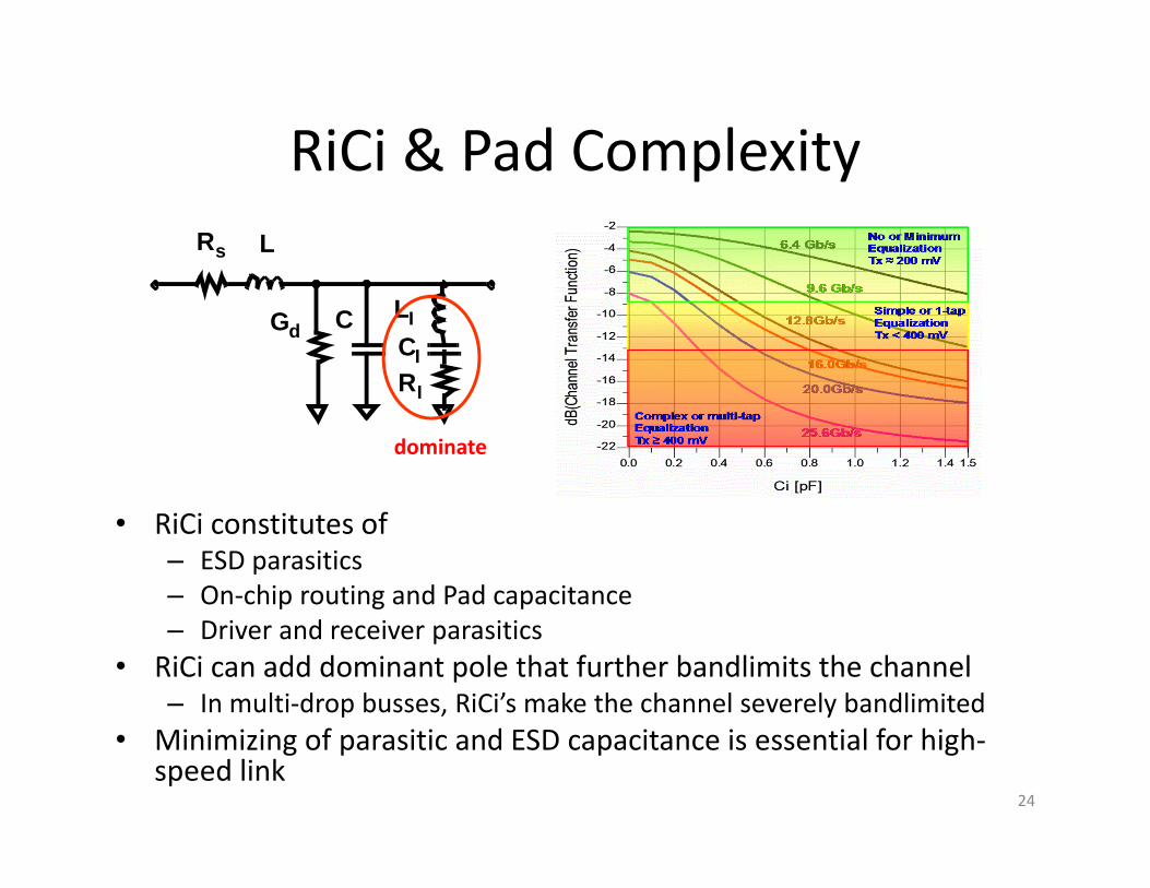
RiCi & Pad Complexity
• RiCi constitutes of – ESD parasitics– On‐chip routing and Pad capacitance– Driver and receiver parasitics
• RiCi can add dominant pole that further bandlimits the channel– In multi‐drop busses, RiCi’s make the channel severely bandlimited
• Minimizing of parasitic and ESD capacitance is essential for high‐speed link
24
LICI
Rs L
CGd
RI
dominate
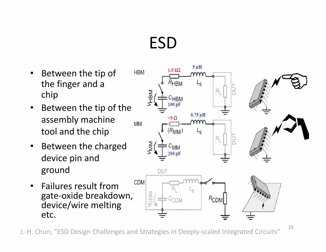
ESD
• Failures result from gate‐oxide breakdown, device/wire melting etc.
25
• Between the tip of the finger and a chip
• Between the tip of the assembly machine tool and the chip
• Between the charged device pin and ground
J.‐H. Chun, “ESD Design Challenges and Strategies in Deeply‐scaled Integrated Circuits”
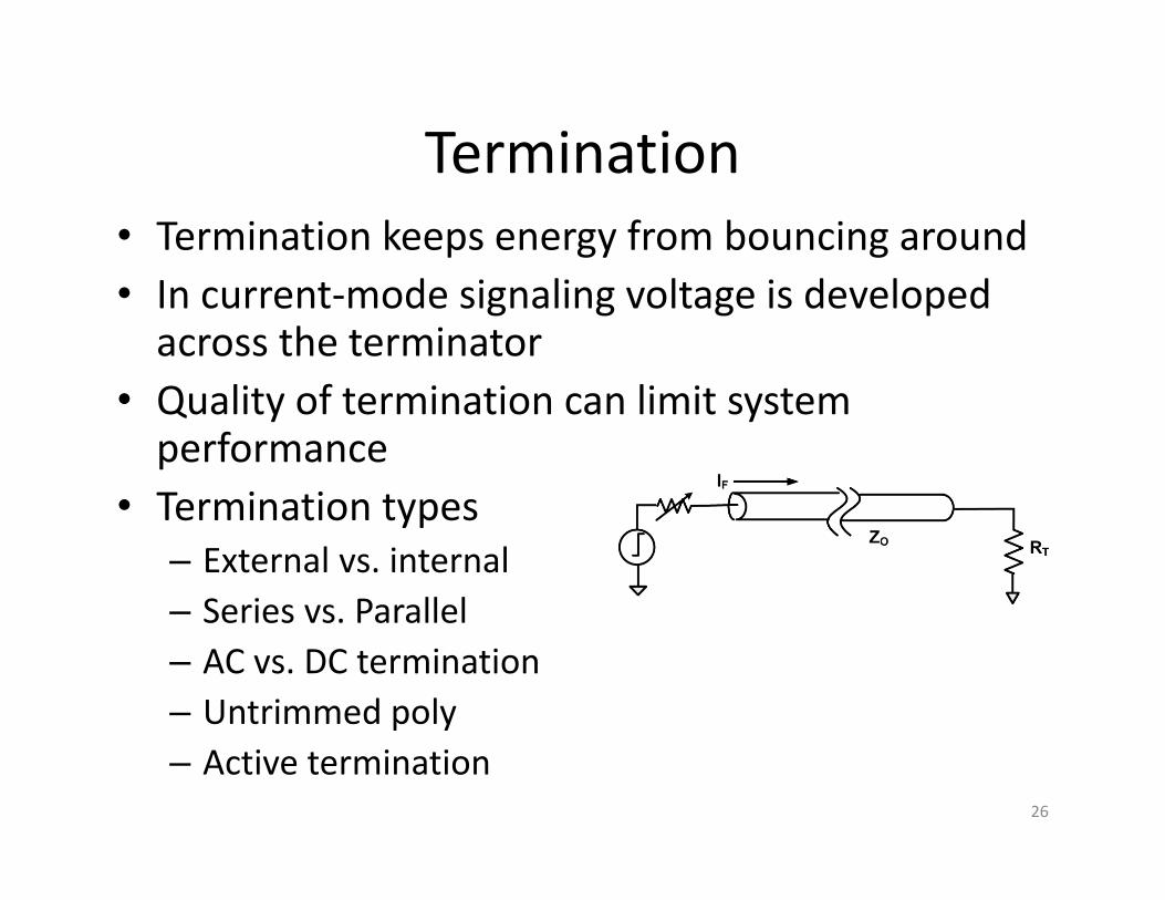
Termination• Termination keeps energy from bouncing around• In current‐mode signaling voltage is developed across the terminator
• Quality of termination can limit system performance
• Termination types– External vs. internal– Series vs. Parallel– AC vs. DC termination– Untrimmed poly– Active termination
26
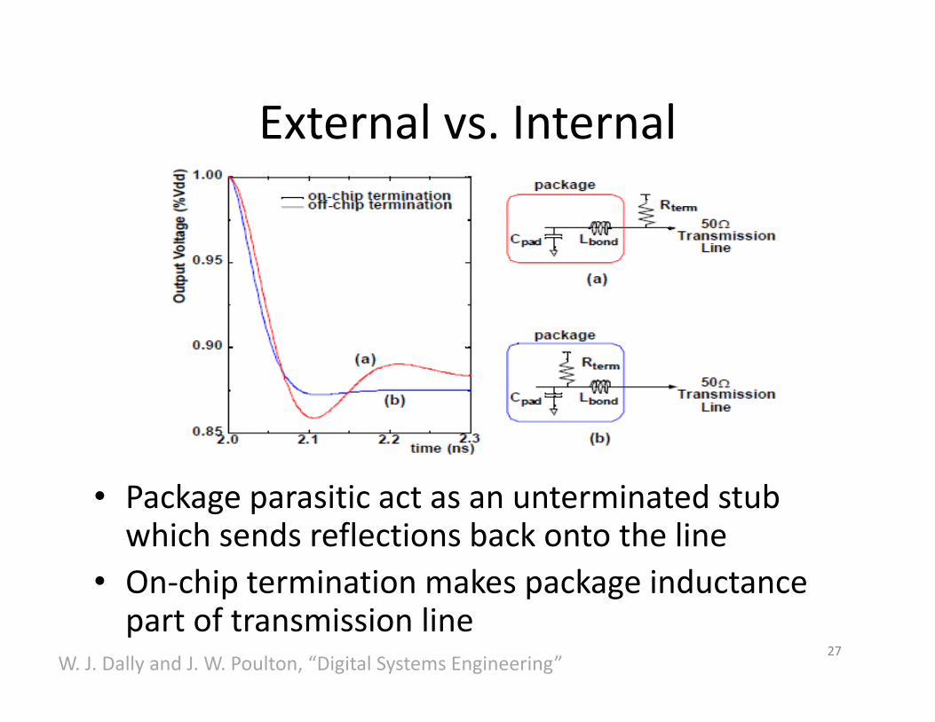
External vs. Internal
• Package parasitic act as an unterminated stub which sends reflections back onto the line
• On‐chip termination makes package inductance part of transmission line
27W. J. Dally and J. W. Poulton, “Digital Systems Engineering”
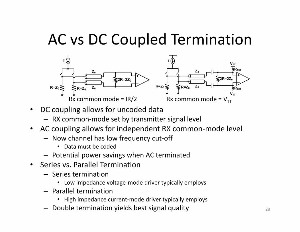
AC vs DC Coupled Termination
• DC coupling allows for uncoded data– RX common‐mode set by transmitter signal level
• AC coupling allows for independent RX common‐mode level– Now channel has low frequency cut‐off
• Data must be coded– Potential power savings when AC terminated
• Series vs. Parallel Termination– Series termination
• Low impedance voltage‐mode driver typically employs – Parallel termination
• High impedance current‐mode driver typically employs – Double termination yields best signal quality
Rx common mode = IR/2 Rx common mode = VTT
28
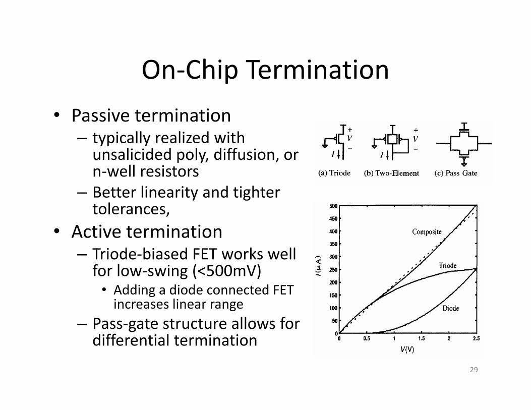
On‐Chip Termination• Passive termination
– typically realized with unsalicided poly, diffusion, or n‐well resistors
– Better linearity and tighter tolerances,
• Active termination– Triode‐biased FET works well for low‐swing (<500mV)
• Adding a diode connected FET increases linear range
– Pass‐gate structure allows for differential termination
29
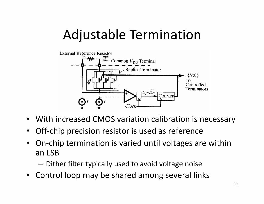
Adjustable Termination
• With increased CMOS variation calibration is necessary • Off‐chip precision resistor is used as reference• On‐chip termination is varied until voltages are within an LSB– Dither filter typically used to avoid voltage noise
• Control loop may be shared among several links30
Tx Slew Rate Control• Output stage slew rate is controlled to reduce noise– Crosstalk noise– Simultaneous switching noise– Reflections at discontinuities
• Too slow→ Limits max data rate• Slew rate control is accomplished by controlling the pre‐driver delay and/or pre‐driver strength
• Output stage is divided and pre‐drive signal is designed to sequentially arrive at the different sections
31
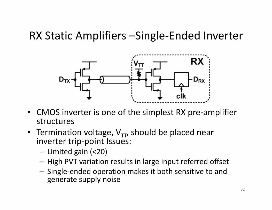
RX Static Amplifiers –Single‐Ended Inverter
• CMOS inverter is one of the simplest RX pre‐amplifier structures
• Termination voltage, VTT, should be placed near inverter trip‐point Issues:– Limited gain (<20)– High PVT variation results in large input referred offset– Single‐ended operation makes it both sensitive to and generate supply noise
32
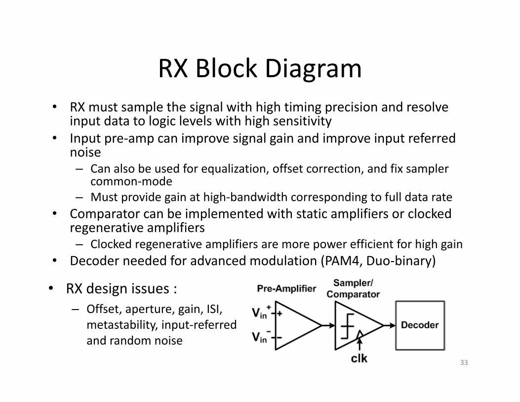
RX Block Diagram• RX must sample the signal with high timing precision and resolve
input data to logic levels with high sensitivity• Input pre‐amp can improve signal gain and improve input referred
noise– Can also be used for equalization, offset correction, and fix sampler
common‐mode– Must provide gain at high‐bandwidth corresponding to full data rate
• Comparator can be implemented with static amplifiers or clocked regenerative amplifiers– Clocked regenerative amplifiers are more power efficient for high gain
• Decoder needed for advanced modulation (PAM4, Duo‐binary)
33
• RX design issues :– Offset, aperture, gain, ISI,
metastability, input‐referred and random noise
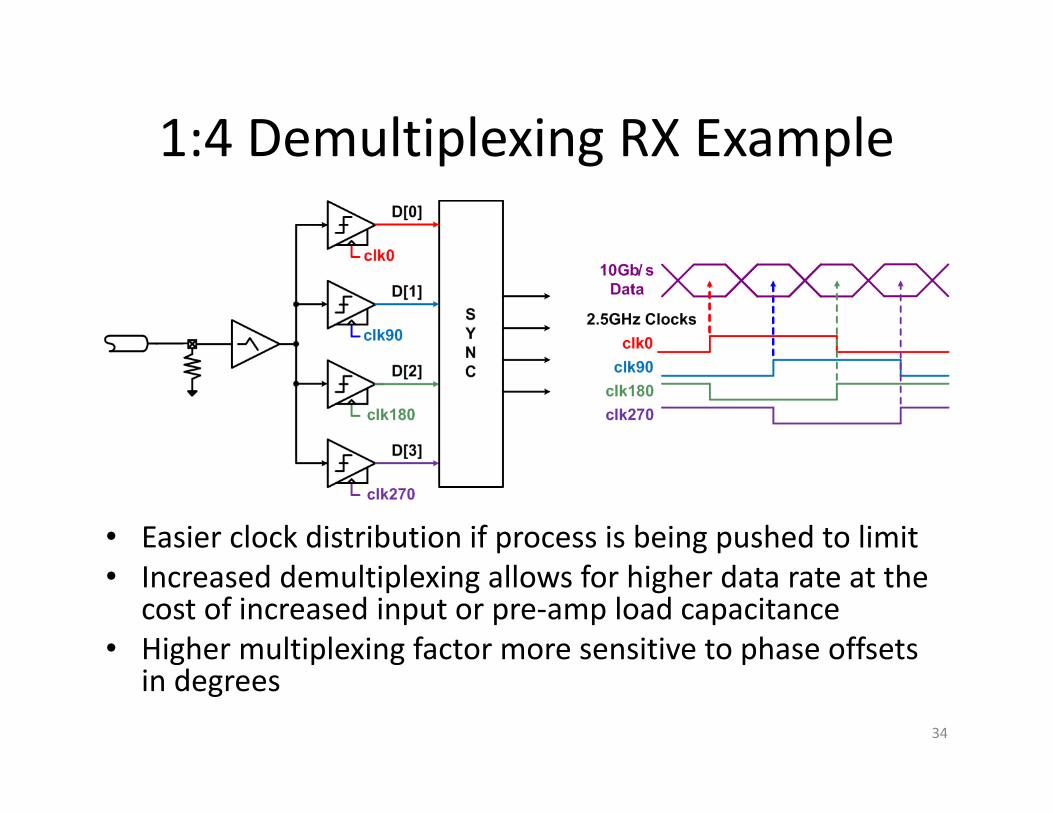
1:4 Demultiplexing RX Example
• Easier clock distribution if process is being pushed to limit• Increased demultiplexing allows for higher data rate at the
cost of increased input or pre‐amp load capacitance• Higher multiplexing factor more sensitive to phase offsets
in degrees34
14 16 18 20 22 24 1416
1820
2224-10
-8
-6
-4
-2
0
Log(
BER
)
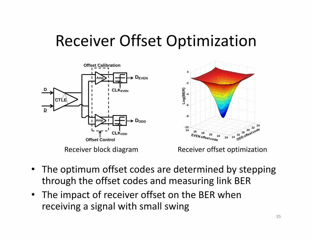
Offset Calibration
CTLE
Offset Control
D
D
DEVEN
DODD
Amp
Amp
CLKEVEN
CLKODD
Receiver Offset Optimization
• The optimum offset codes are determined by stepping through the offset codes and measuring link BER
• The impact of receiver offset on the BER when receiving a signal with small swing
Receiver block diagram Receiver offset optimization
35
Outline
• Introduction and Overview• High‐Speed Channel• I/O Circuits• Equalization• Clocking and Timing • Advanced Signaling and Coding• Performance Evaluation• Summary
36
• Receive Linear Equalization• Transmit Linear Equalization• Rx Linear EQ• RX DFE• Setting coefficients
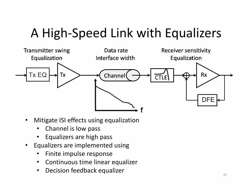
A High‐Speed Link with Equalizers
• Mitigate ISI effects using equalization• Channel is low pass• Equalizers are high pass
• Equalizers are implemented using• Finite impulse response • Continuous time linear equalizer• Decision feedback equalizer
37
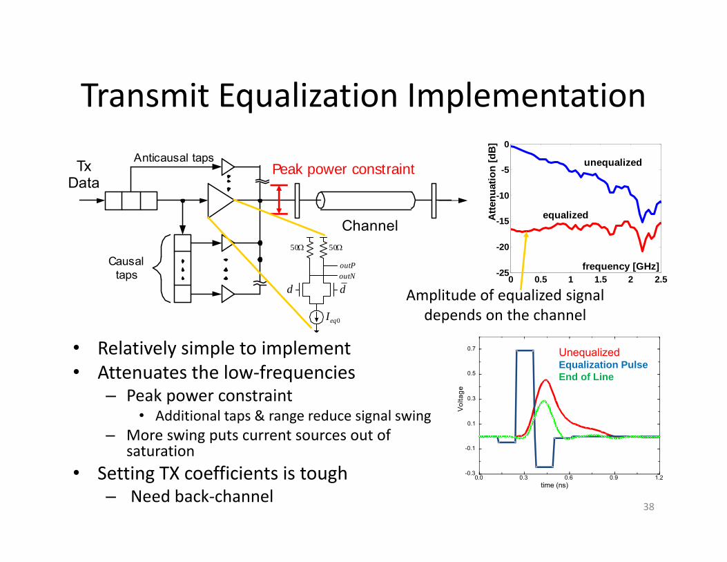
• Relatively simple to implement• Attenuates the low‐frequencies
– Peak power constraint• Additional taps & range reduce signal swing
– More swing puts current sources out of saturation
• Setting TX coefficients is tough– Need back‐channel
Transmit Equalization Implementation
38
0 0.5 1 1.5 2 2.5-25
-20
-15
-10
-5
0
frequency [GHz]
Atte
nuat
ion
[dB
]
equalized
unequalized
Amplitude of equalized signaldepends on the channel
TxData
Causaltaps
Anticausal taps
Channel
Peak power constraint
0eqI
doutNoutP
d
5050
0.0 0.3 0.6 0.9 1.2-0.3
-0.1
0.1
0.3
0.5
0.7UnequalizedEqualization PulseEnd of Line
time (ns)
Vol
tage
UnequalizedEqualization PulseEnd of Line
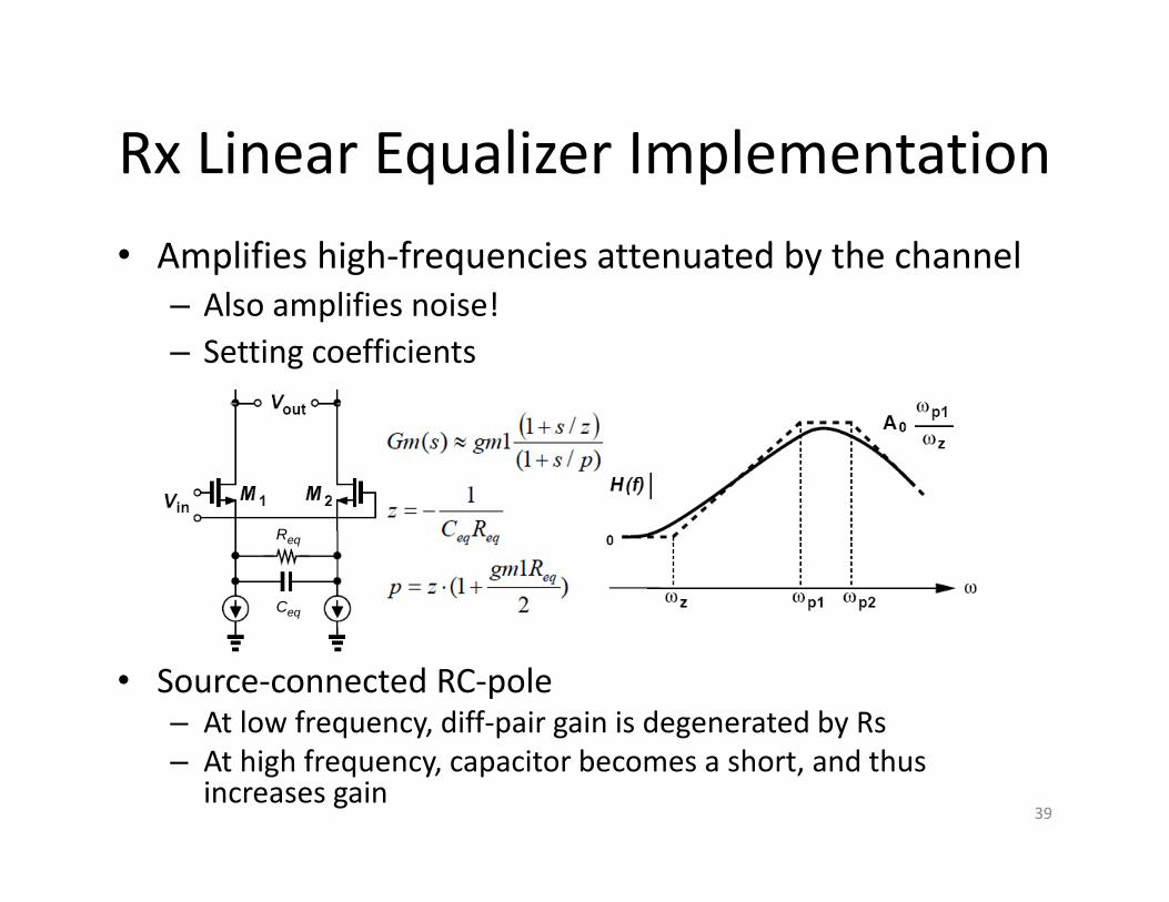
Rx Linear Equalizer Implementation
• Source‐connected RC‐pole– At low frequency, diff‐pair gain is degenerated by Rs– At high frequency, capacitor becomes a short, and thus
increases gain39
Ceq
Req
• Amplifies high‐frequencies attenuated by the channel– Also amplifies noise!– Setting coefficients
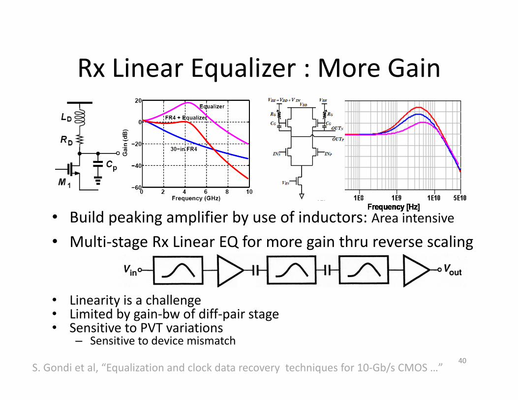
Rx Linear Equalizer : More Gain
• Build peaking amplifier by use of inductors: Area intensive• Multi‐stage Rx Linear EQ for more gain thru reverse scaling
40
• Linearity is a challenge• Limited by gain‐bw of diff‐pair stage• Sensitive to PVT variations
– Sensitive to device mismatch
S. Gondi et al, “Equalization and clock data recovery techniques for 10‐Gb/s CMOS …”
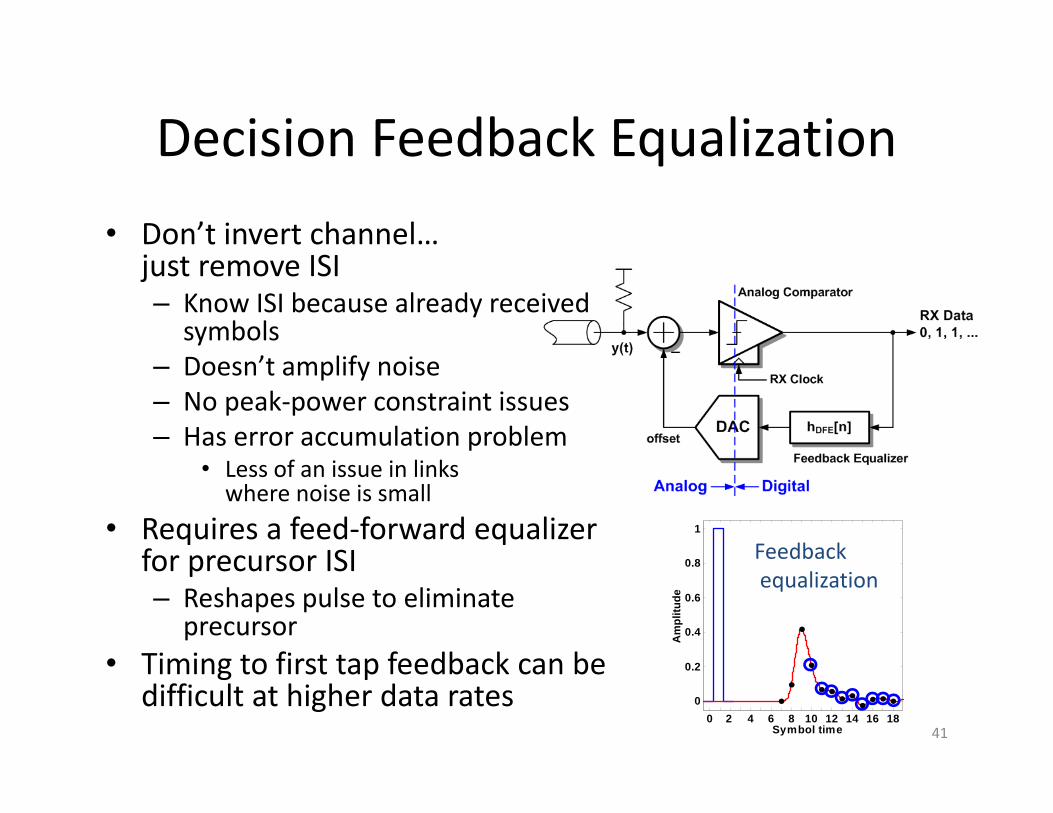
Decision Feedback Equalization• Don’t invert channel…
just remove ISI– Know ISI because already received
symbols– Doesn’t amplify noise– No peak‐power constraint issues– Has error accumulation problem
• Less of an issue in linkswhere noise is small
• Requires a feed‐forward equalizer for precursor ISI– Reshapes pulse to eliminate
precursor• Timing to first tap feedback can be
difficult at higher data rates41
0 2 4 6 8 10 12 14 16 180
0.2
0.4
0.6
0.8
1
Symbol time
Am
plitu
de
Feedbackequalization
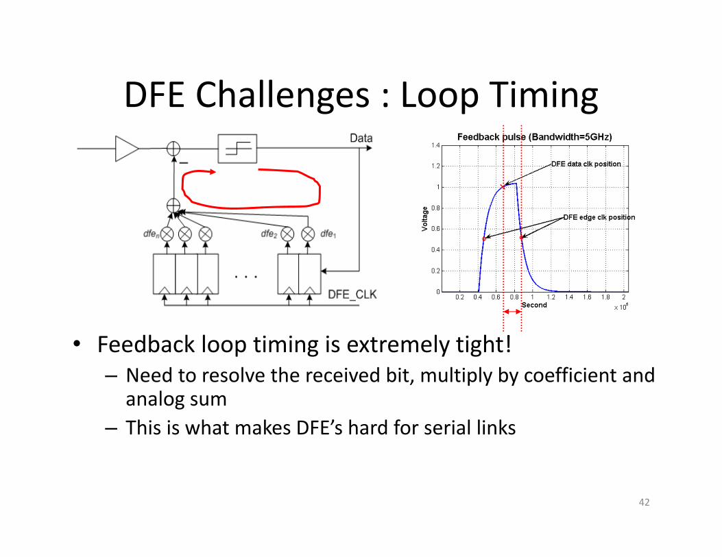
DFE Challenges : Loop Timing
• Feedback loop timing is extremely tight!– Need to resolve the received bit, multiply by coefficient and analog sum
– This is what makes DFE’s hard for serial links
42
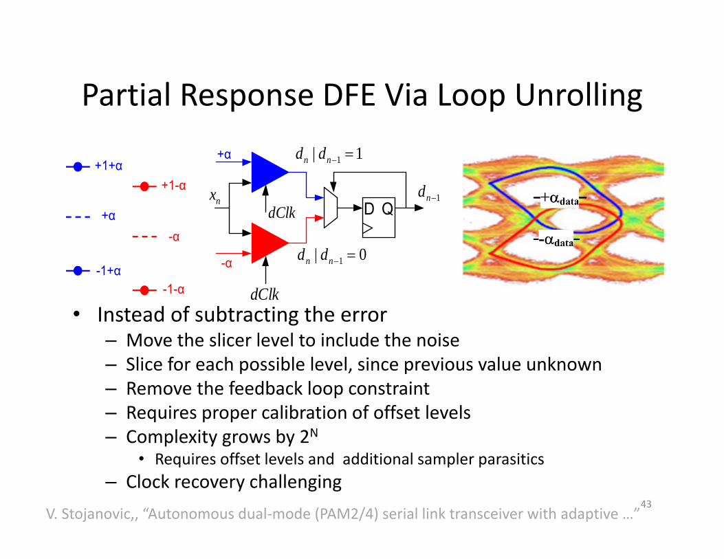
Partial Response DFE Via Loop Unrolling
• Instead of subtracting the error– Move the slicer level to include the noise– Slice for each possible level, since previous value unknown– Remove the feedback loop constraint– Requires proper calibration of offset levels– Complexity grows by 2N
• Requires offset levels and additional sampler parasitics– Clock recovery challenging
43
+1+α
-1+α
+α
+1-α
-1-α
-α
D Q1nd
dClk
1| 1 nn dd
0| 1 nn dd
dClknx
+α
-α
V. Stojanovic,, “Autonomous dual‐mode (PAM2/4) serial link transceiver with adaptive …”
Equalizer Optimization Algorithms• Two Types :ZF vs. MMSE
– ZF (Zero‐Forcing) • Direct and easy to implement• ZF implies infinite filter gain at points of singularity
– (MMSE) Minimum‐Mean‐Square Error• ZF amplifies noise at those null frequencies• Hence is often preferred over ZF
– If there is no Gaussian noise, ZF=MMSE–
• Three Basic Methods for Setting Equalization Coefficients– Lookup table ‘set and forget’
• Simple, based on lab measurement• Subject to manufacturing and environment variations
– Adapt once on power‐up• More complex• Subject to environment variation
– Continuous adaptation• Most complex• Most complete
44
Outline• Introduction and Overview• High‐Speed Channel• I/O Circuits • Equalization• Clocking and Timing • Advanced Signaling and Coding• Performance Evaluation• Summary
45
• Clocking overview• Common clock• Source synchronous • Embedded clocks • Asynchronous systems
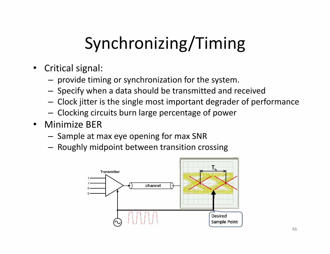
Synchronizing/Timing• Critical signal:
– provide timing or synchronization for the system.– Specify when a data should be transmitted and received– Clock jitter is the single most important degrader of performance– Clocking circuits burn large percentage of power
• Minimize BER– Sample at max eye opening for max SNR– Roughly midpoint between transition crossing
46
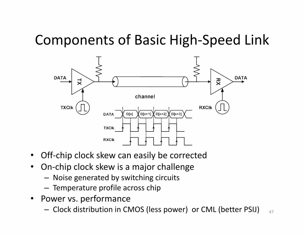
Components of Basic High‐Speed Link
• Off‐chip clock skew can easily be corrected• On‐chip clock skew is a major challenge
– Noise generated by switching circuits– Temperature profile across chip
• Power vs. performance– Clock distribution in CMOS (less power) or CML (better PSIJ) 47
Phase‐Locked and Delay‐Locked Loops
• PLLs and DLLs find wide application in areas such as communications, wireless systems, digital circuits and disk‐drive electronics.
• Benefits:– Jitter Reduction– Skew Suppression– Frequency Synthesis– Clock Recovery
• Minimize BER– Sample at max eye opening for max SNR– Roughly midpoint between transition crossing– Timing information of data transitions required
48
I/O Clocking Architectures
• Three basic I/O architectures – Common Clock (Synchronous) – Forward Clock (Source Synchronous)– Embedded Clock (Clock Recovery)
• These I/O architectures are used for varying applications that require different levels of I/O bandwidth
• A processor may have one or all of these I/O types• Often the same circuitry can be used to emulate different I/O schemes for design reuse
49
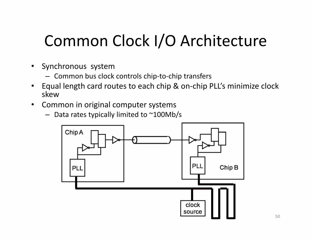
Common Clock I/O Architecture• Synchronous system
– Common bus clock controls chip‐to‐chip transfers• Equal length card routes to each chip & on‐chip PLL’s minimize clock
skew• Common in original computer systems
– Data rates typically limited to ~100Mb/s
50
Common Clock I/O Limitations
• Difficult to control clock skew and propagation delay
• Need to have tight control of absolute delay to meet a given cycle time
• Sensitive to delay variations in on‐chip circuits and board routes
• Hard to compensate for delay variations due to low correlation between on‐chip and off‐chip delays
• While commonly used in on‐chip communication, offers limited speed in off‐chip I/O applications
51
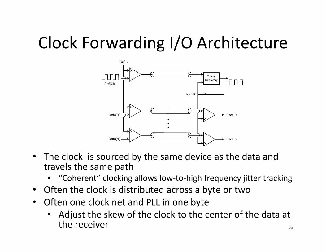
Clock Forwarding I/O Architecture
• The clock is sourced by the same device as the data and travels the same path• “Coherent” clocking allows low‐to‐high frequency jitter tracking
• Often the clock is distributed across a byte or two• Often one clock net and PLL in one byte
• Adjust the skew of the clock to the center of the data at the receiver 52
Clock Forwarding I/O De‐Skew
• Per‐channel de‐skew allows for significant data rate increases
• Sample clock adjusted to center clock on the incoming data eye
• Implementations– Delay‐Locked Loop and Phase Interpolators– Injection‐Locked Oscillators
• Clock forwarding I/O limitations– Low pass channel causes jitter amplification
• 20 dB channel loss could result 5X DCD amplification– Clock skew can limit forward clock I/O performance
53
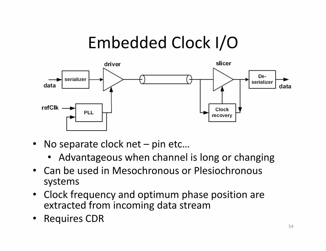
Embedded Clock I/O
• No separate clock net – pin etc…• Advantageous when channel is long or changing
• Can be used in Mesochronous or Plesiochronoussystems
• Clock frequency and optimum phase position are extracted from incoming data stream
• Requires CDR54
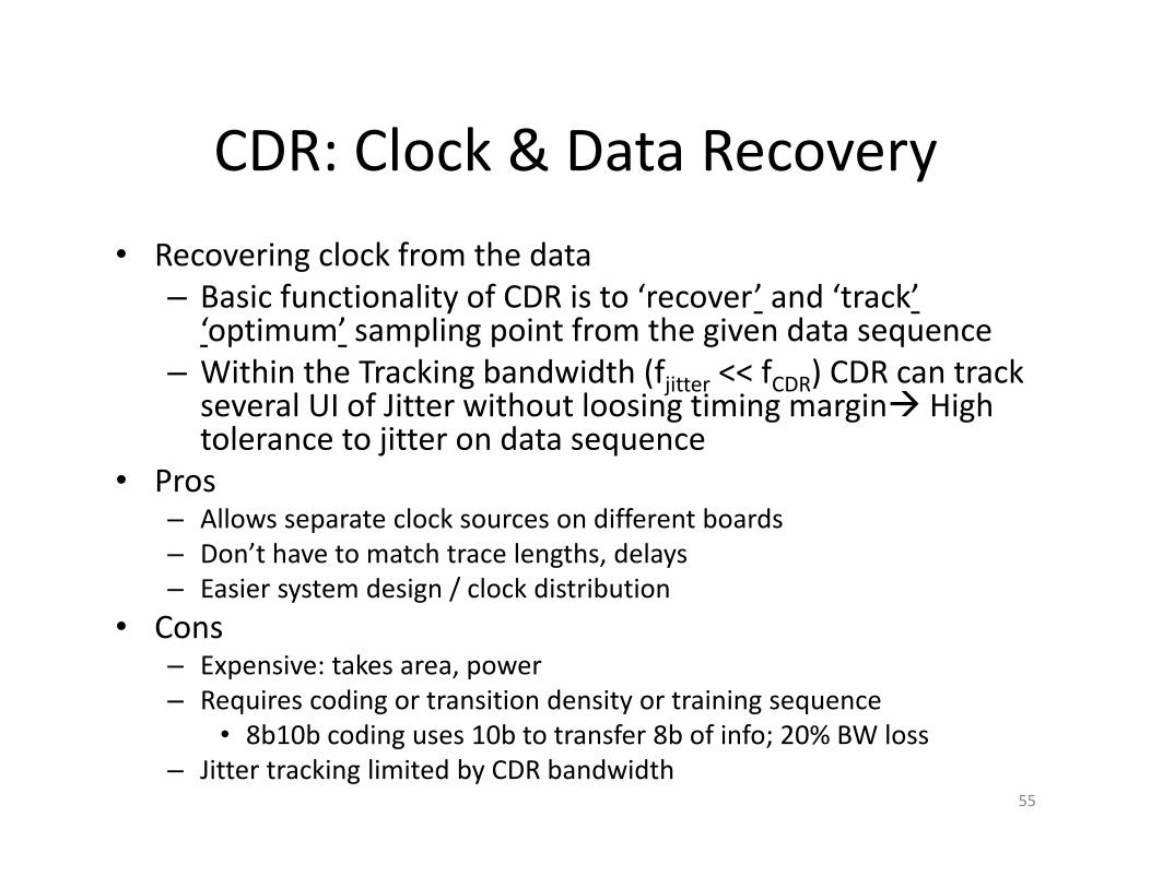
CDR: Clock & Data Recovery• Recovering clock from the data
– Basic functionality of CDR is to ‘recover’ and ‘track’‘optimum’ sampling point from the given data sequence
– Within the Tracking bandwidth (fjitter << fCDR) CDR can track several UI of Jitter without loosing timing margin High tolerance to jitter on data sequence
• Pros– Allows separate clock sources on different boards– Don’t have to match trace lengths, delays– Easier system design / clock distribution
• Cons– Expensive: takes area, power– Requires coding or transition density or training sequence
• 8b10b coding uses 10b to transfer 8b of info; 20% BW loss– Jitter tracking limited by CDR bandwidth
55
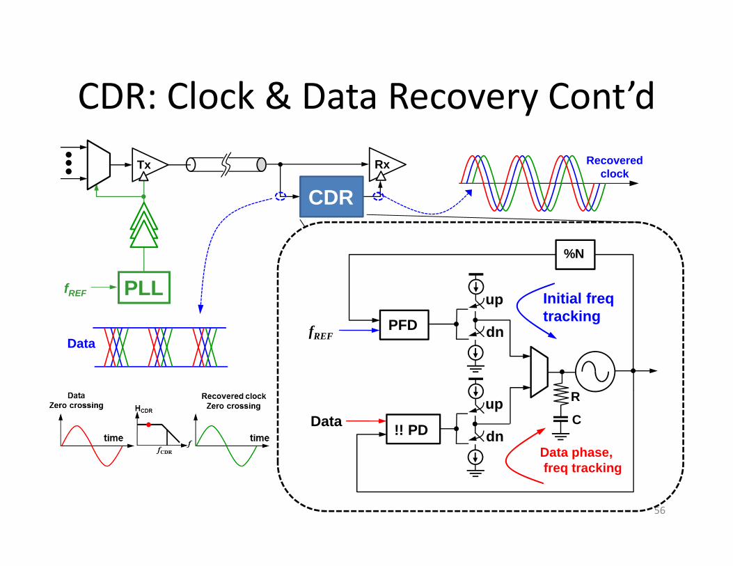
CDR: Clock & Data Recovery Cont’d
56
PLL
Tx Rx
fREF
CDR
R
Cup
dn
PFDfREF
up
dn
!! PDData
%N
Initial freqtracking
Data phase,freq tracking
Data
Recoveredclock
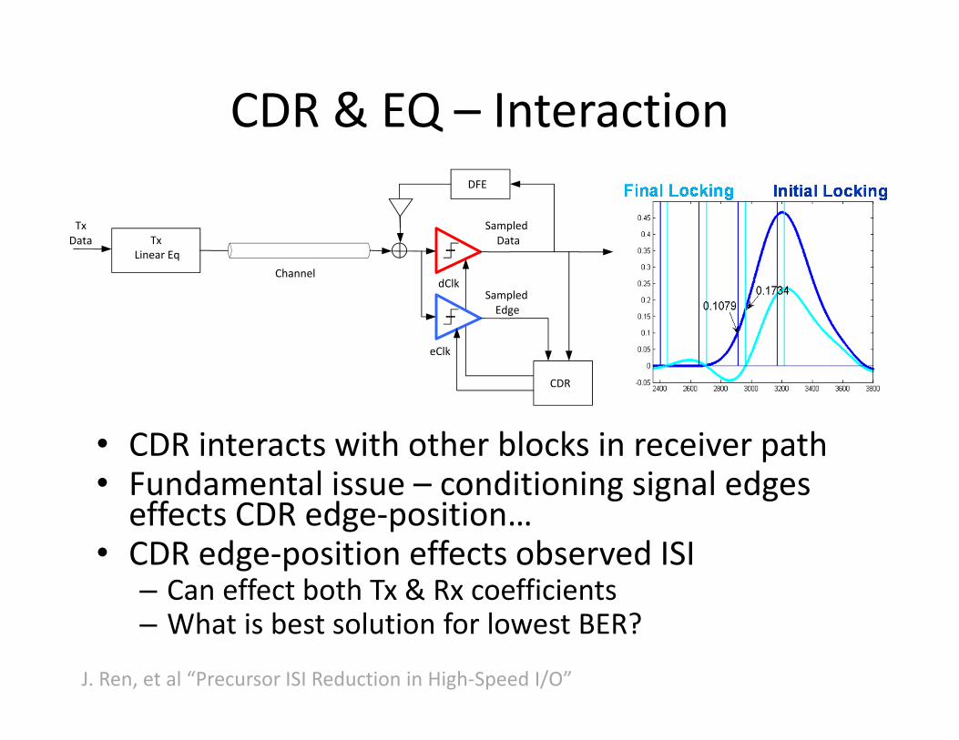
CDR & EQ – Interaction
• CDR interacts with other blocks in receiver path• Fundamental issue – conditioning signal edges effects CDR edge‐position…
• CDR edge‐position effects observed ISI– Can effect both Tx & Rx coefficients– What is best solution for lowest BER?
Tx Linear Eq
Channel
CDR
DFE
dClk
eClk
SampledData
Sampled Edge
Tx Data
J. Ren, et al “Precursor ISI Reduction in High‐Speed I/O”
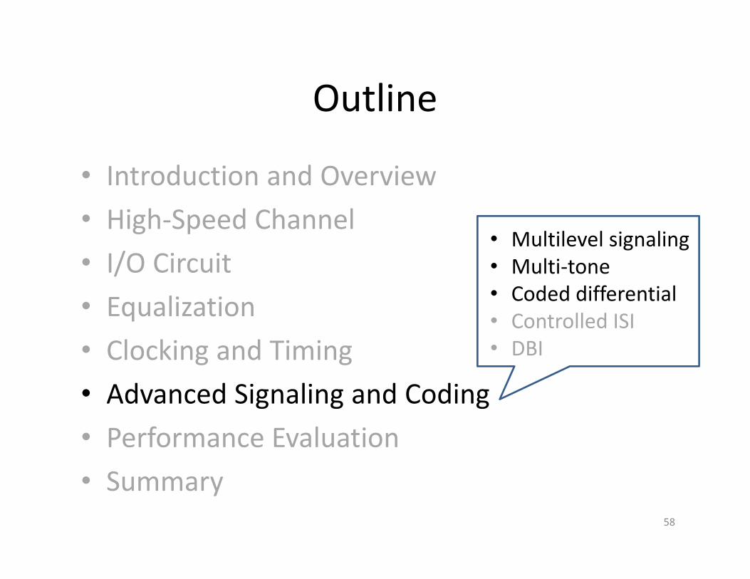
Outline
• Introduction and Overview• High‐Speed Channel• I/O Circuit • Equalization• Clocking and Timing • Advanced Signaling and Coding• Performance Evaluation• Summary
58
• Multilevel signaling• Multi‐tone• Coded differential • Controlled ISI• DBI
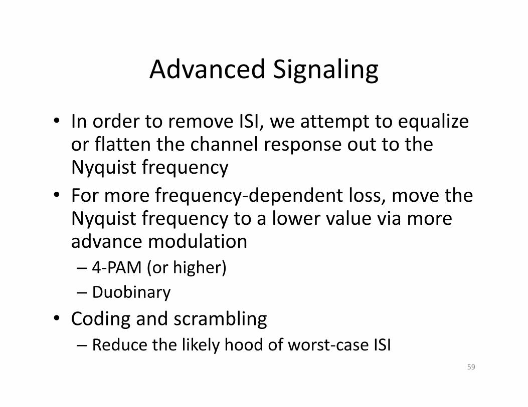
Advanced Signaling
• In order to remove ISI, we attempt to equalize or flatten the channel response out to the Nyquist frequency
• For more frequency‐dependent loss, move the Nyquist frequency to a lower value via more advance modulation– 4‐PAM (or higher)– Duobinary
• Coding and scrambling– Reduce the likely hood of worst‐case ISI
59
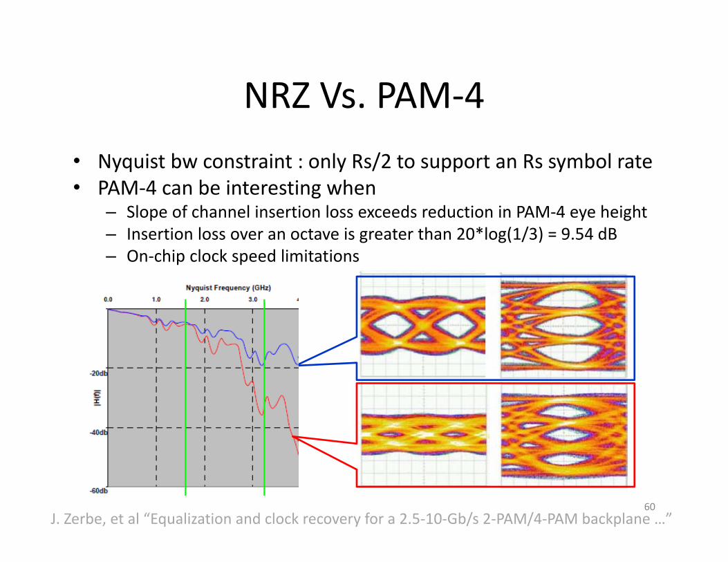
NRZ Vs. PAM‐4• Nyquist bw constraint : only Rs/2 to support an Rs symbol rate• PAM‐4 can be interesting when
– Slope of channel insertion loss exceeds reduction in PAM‐4 eye height– Insertion loss over an octave is greater than 20*log(1/3) = 9.54 dB– On‐chip clock speed limitations
60J. Zerbe, et al “Equalization and clock recovery for a 2.5‐10‐Gb/s 2‐PAM/4‐PAM backplane …”
Multi‐Level PAM Challenges• Need to balance with Tx, RX circuit complexity
– Advanced equalization (DFE) can allow NRZ signaling to have comparable (or better) performance even with > 9.5dB loss per octave
• Receiver complexity increases considerably– 3x input comparators (2‐bit ADC)– Input signal is no longer self‐referenced at 0V differential
– DFE complexity doubles if required• CDR can display extra jitter due to multiple “zero crossing” times
• Smaller eyes are more sensitive to crosstalk due to maximum transitions
61
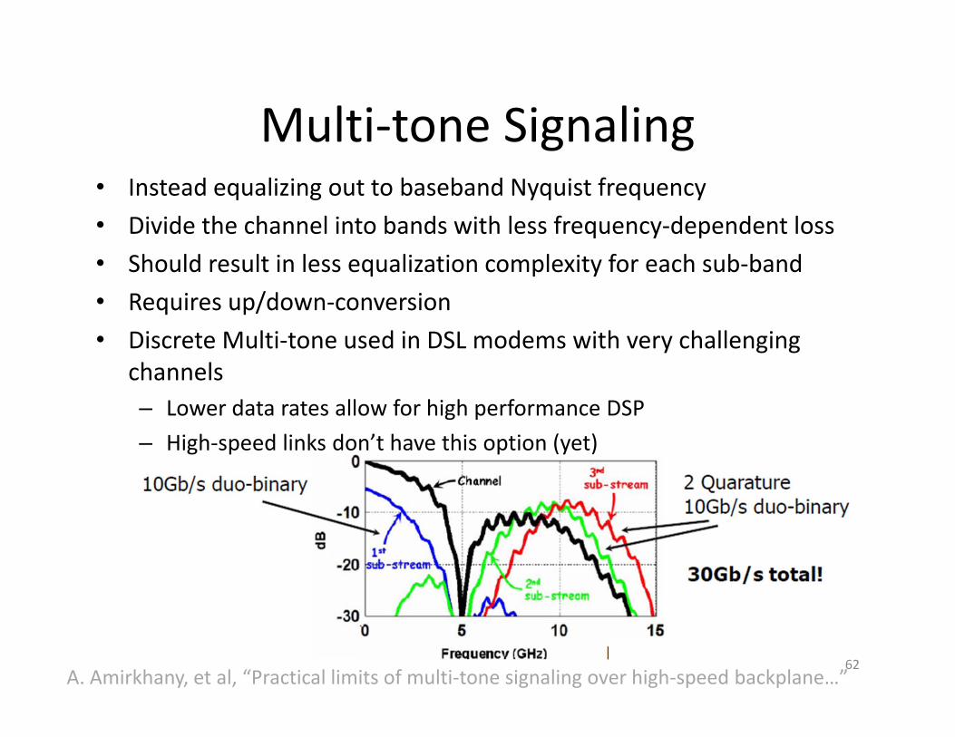
Multi‐tone Signaling• Instead equalizing out to baseband Nyquist frequency• Divide the channel into bands with less frequency‐dependent loss• Should result in less equalization complexity for each sub‐band• Requires up/down‐conversion• Discrete Multi‐tone used in DSL modems with very challenging
channels– Lower data rates allow for high performance DSP– High‐speed links don’t have this option (yet)
62A. Amirkhany, et al, “Practical limits of multi‐tone signaling over high‐speed backplane…”
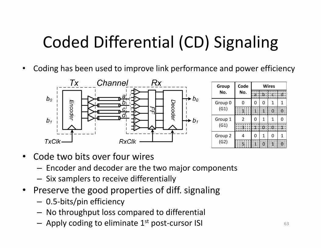
Coded Differential (CD) Signaling
• Code two bits over four wires– Encoder and decoder are the two major components– Six samplers to receive differentially
• Preserve the good properties of diff. signaling– 0.5‐bits/pin efficiency – No throughput loss compared to differential– Apply coding to eliminate 1st post‐cursor ISI 63
Group No.
CodeNo.
Wires
a b c d
Group 0 (G1)
0 0 0 1 1
1 1 1 0 0
Group 1 (G1)
2 0 1 1 0
3 1 0 0 1
Group 2 (G2)
4 0 1 0 1
5 1 0 1 0
• Coding has been used to improve link performance and power efficiency
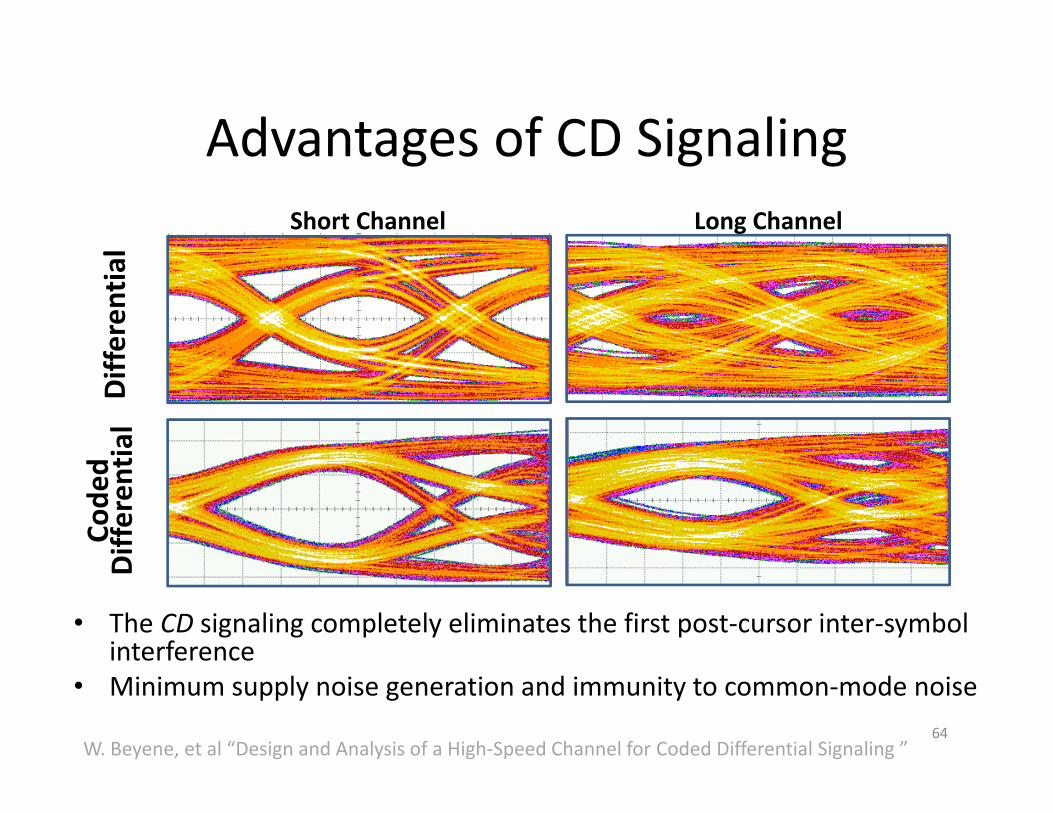
Advantages of CD SignalingShort Channel Long Channel
Differen
tial
Code
dDifferen
tial
64
• The CD signaling completely eliminates the first post‐cursor inter‐symbol interference
• Minimum supply noise generation and immunity to common‐mode noise
W. Beyene, et al “Design and Analysis of a High‐Speed Channel for Coded Differential Signaling ”
Outline
• Introduction and Overview• High‐Speed Channel• I/O Circuits• Equalization• Clocking and Timing • Advanced Signaling and Coding• Performance Evaluation• Summary
65
• Link simulation• Link measurement• Link budget
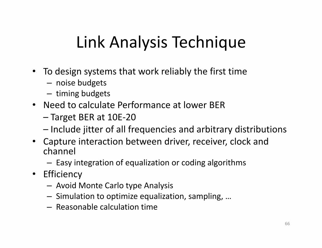
Link Analysis Technique• To design systems that work reliably the first time
– noise budgets– timing budgets
• Need to calculate Performance at lower BER– Target BER at 10E‐20– Include jitter of all frequencies and arbitrary distributions
• Capture interaction between driver, receiver, clock and channel– Easy integration of equalization or coding algorithms
• Efficiency– Avoid Monte Carlo type Analysis– Simulation to optimize equalization, sampling, …– Reasonable calculation time
66
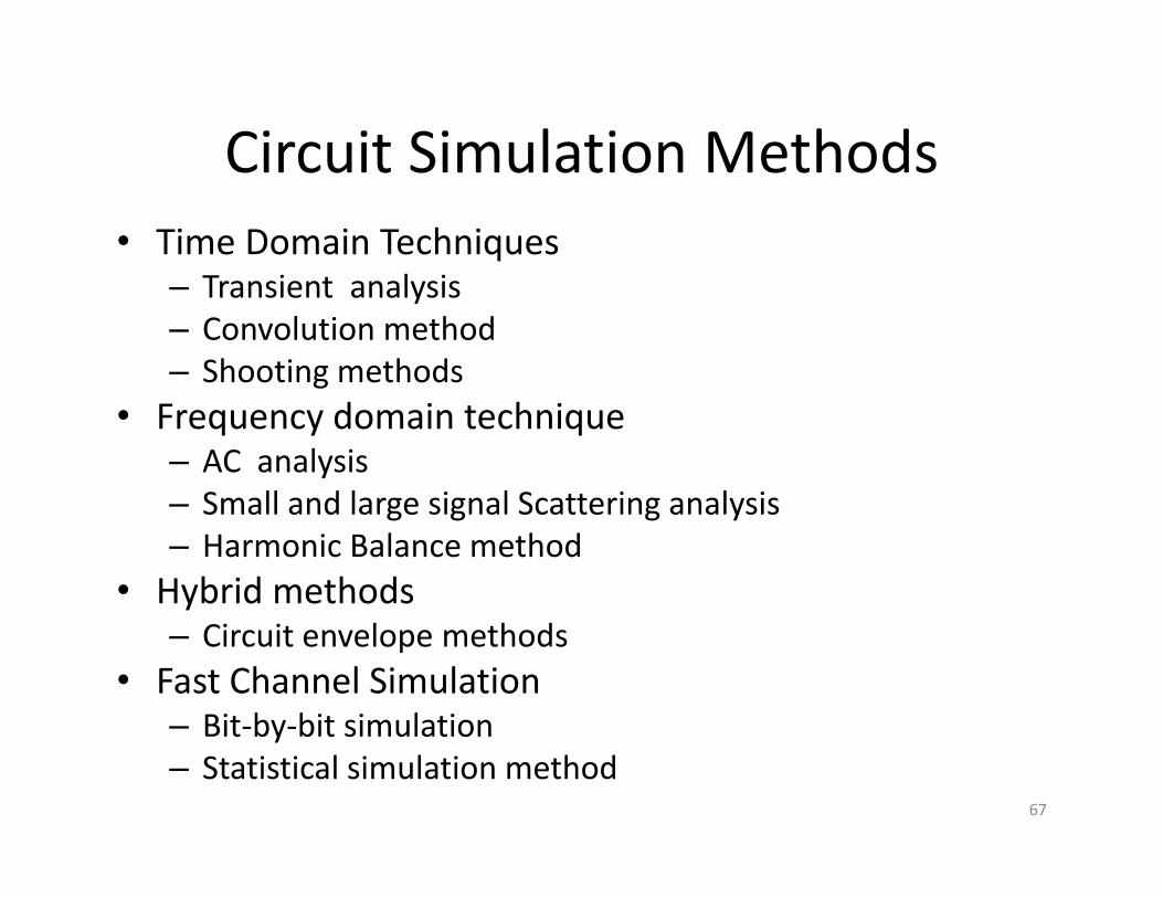
Circuit Simulation Methods• Time Domain Techniques
– Transient analysis– Convolution method– Shooting methods
• Frequency domain technique– AC analysis– Small and large signal Scattering analysis– Harmonic Balance method
• Hybrid methods– Circuit envelope methods
• Fast Channel Simulation– Bit‐by‐bit simulation– Statistical simulation method
67

Advantage Fast Channel Simulation• Accurate reprentation of channel using S‐parameter
– Direct convolution : model order reduction method• Interaction between circuit and channel characteristics• Compare different modulation techniques: NRZ, partial signaling, ...• Quantify performance improvement and cost due
– Better package, low‐loss PCB laminate– better board ref clock– backdrill vias– improved supply filtering
• Relate PLL jitter to BER or max data rate.• Quantify the minimum PLL BW (before failure).• What type of equalization should I use?
– Know how well equalizer coefficients can be optimized using adaptive control• Evaluate impact of spread spectrum : data rate reduction • Decide where I should put most of my design effort.
– PLL, DLL, buffer, equalizer, RX
68A. Sanders, “Statistical simulation of physical transmission media”
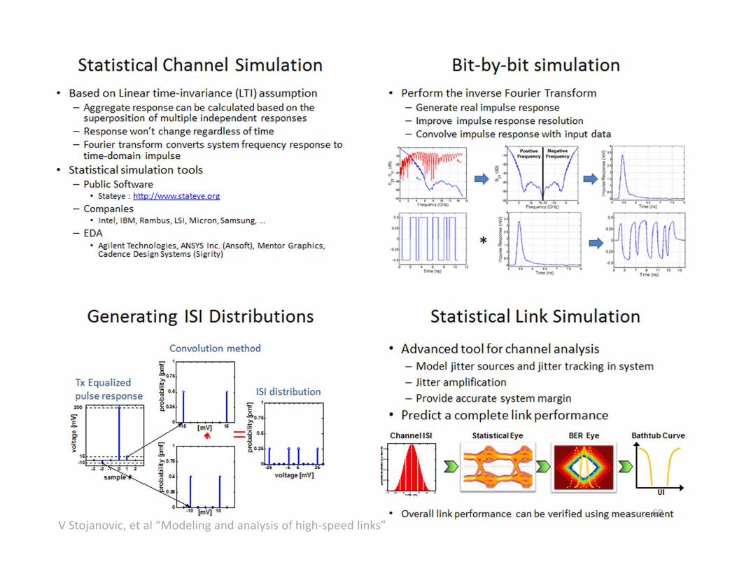
69V Stojanovic, et al “Modeling and analysis of high‐speed links”
Measurements of Complete Link• On‐bench measurements can be limited by
– Stub effects– Probe loading effects
• On‐chip measurement techniques can allow us – To accurately characterize high‐speed links– To capture the interaction between passive and active circuits
• Indirect measurement and on‐chip measurement techniques enable us to characterize components or link that are not easily observable
• Time and frequency‐domain responses from on‐chip and on‐bench measurements are correlated
70
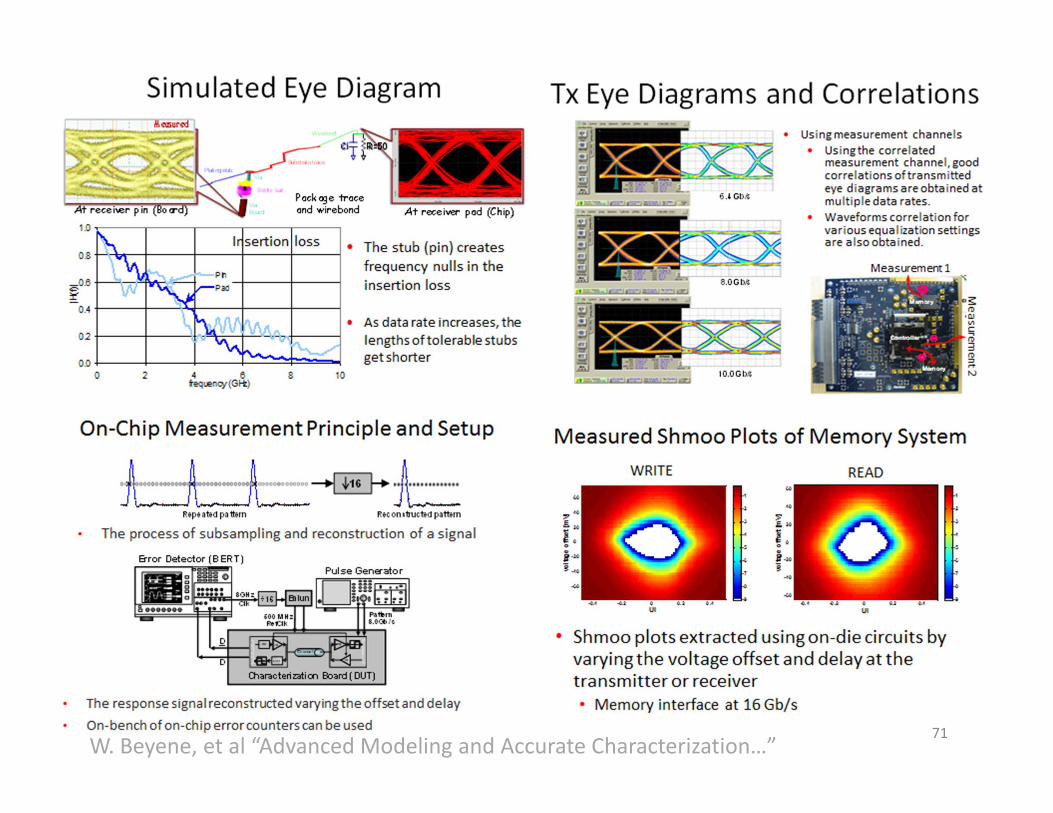
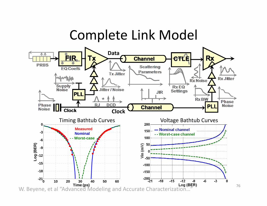
71W. Beyene, et al “Advanced Modeling and Accurate Characterization…”
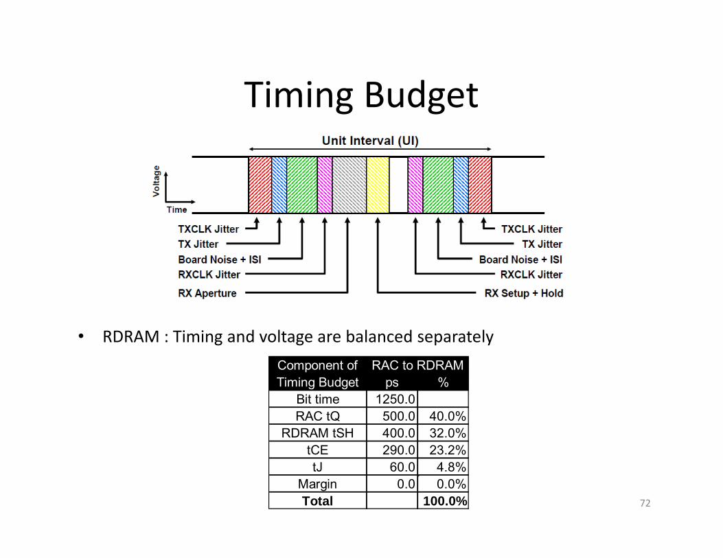
Timing Budget
72
Component of RAC to RDRAMTiming Budget ps %
Bit time 1250.0RAC tQ 500.0 40.0%
RDRAM tSH 400.0 32.0%tCE 290.0 23.2%tJ 60.0 4.8%
Margin 0.0 0.0%Total 100.0%
• RDRAM : Timing and voltage are balanced separately
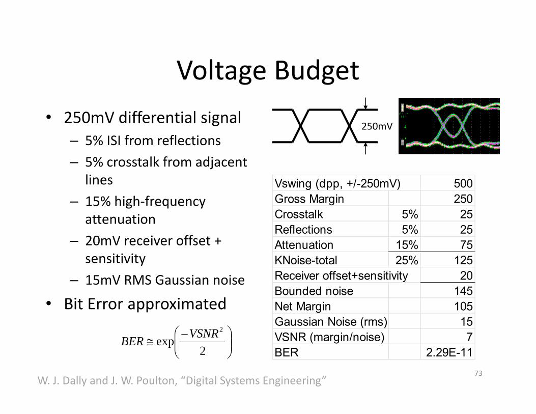
Voltage Budget• 250mV differential signal
– 5% ISI from reflections– 5% crosstalk from adjacent
lines– 15% high‐frequency
attenuation– 20mV receiver offset +
sensitivity– 15mV RMS Gaussian noise
• Bit Error approximated
73
2exp
2VSNRBER
250mV
Vswing (dpp, +/-250mV) 500Gross Margin 250Crosstalk 5% 25Reflections 5% 25Attenuation 15% 75KNoise-total 25% 125Receiver offset+sensitivity 20Bounded noise 145Net Margin 105Gaussian Noise (rms) 15VSNR (margin/noise) 7BER 2.29E-11
W. J. Dally and J. W. Poulton, “Digital Systems Engineering”
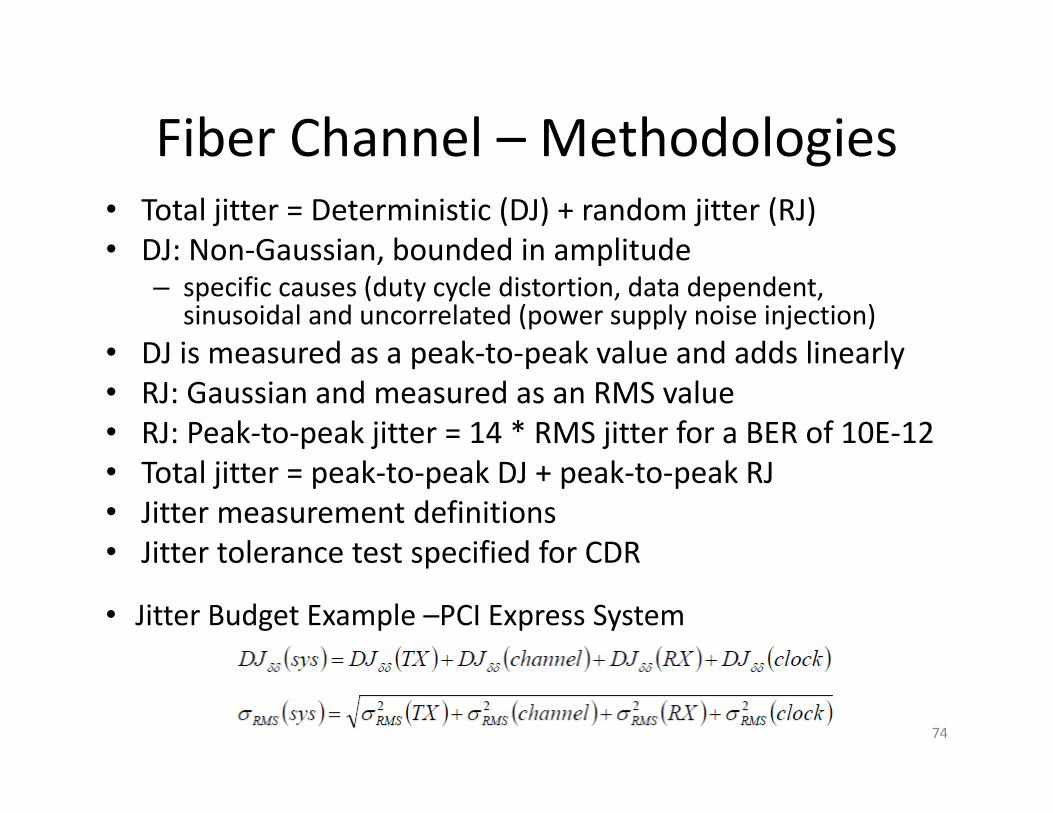
Fiber Channel – Methodologies• Total jitter = Deterministic (DJ) + random jitter (RJ)• DJ: Non‐Gaussian, bounded in amplitude
– specific causes (duty cycle distortion, data dependent, sinusoidal and uncorrelated (power supply noise injection)
• DJ is measured as a peak‐to‐peak value and adds linearly• RJ: Gaussian and measured as an RMS value• RJ: Peak‐to‐peak jitter = 14 * RMS jitter for a BER of 10E‐12• Total jitter = peak‐to‐peak DJ + peak‐to‐peak RJ• Jitter measurement definitions• Jitter tolerance test specified for CDR
74
• Jitter Budget Example –PCI Express System
Link Budget• Newer approach is needed to managing jitter and noise in new generation interfaces– To remove pessimism built in equation based or spread sheet based link budget
– Capture the interaction between off‐chip and on‐chip blocks
– Consider the relationship between voltage noise and timing jitter
– Adopt more realistic jitter and noise models• Consider jitter and noise spectrum• Include jitter/noise enhancement, filtering, and tracking
– Balance budget with power efficient solutions• Both distribution and spectral content need to be considered
75
0 10 20 30 40 50 60-21
-18
-15
-12
-9
-6
-3
0
Time (ps)
Log
(BER
)
MeasuredNominal
- - Worst-case
Timing Bathtub Curves Voltage Bathtub Curves
Complete Link Model
76
Data
Clock
W. Beyene, et al “Advanced Modeling and Accurate Characterization…”
Summary• Accurate modeling and analysis of high‐speed channels
– Surface roughness, Fiber weave effects, …• Interaction between on‐chip circuits and off‐chip components• Interaction between clock recovery and equalization
adaptation loops– CDR and EQ interaction
• Advanced modulation and coding can improve link performance– Multi‐level, multi‐tone, coding
• Fast link simulation – Nonlinearity– Jitter correlation and spectrum– Both voltage noise and timing jitter
• Performance of high‐speed link are verified with both on‐chip and off‐chip measurement techniques 77
Acknowledgments
• A lot of the materials are borrowed from internal and external presentations made by many Rambus engineers
78
Backup Slides Partial Response Signaling
Data Bus Inversion (DC and AC)
79
Controlled ISI Channel Design
• Channel capacity can be improved using controlled inter‐symbol interference (ISI) design technique
• Shaping the channel to match a partial response system by “intentionally” introducing additional loss or impedance discontinuities
• Since the ISI is known or controlled, it can be removed at the receiver– produce correlated signals – converts binary to multilevel signals– also known as Partial‐Response signaling
80
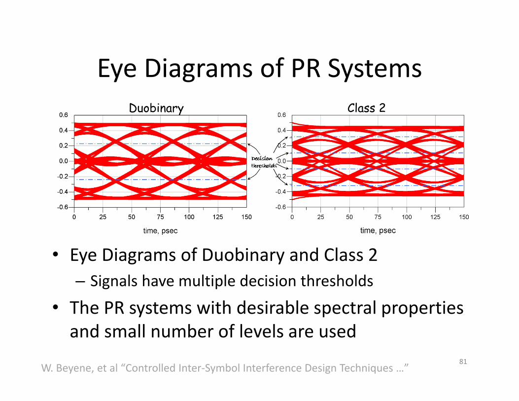
Eye Diagrams of PR Systems
• Eye Diagrams of Duobinary and Class 2 – Signals have multiple decision thresholds
• The PR systems with desirable spectral properties and small number of levels are used
81
Duobinary Class 2
W. Beyene, et al “Controlled Inter‐Symbol Interference Design Techniques …”
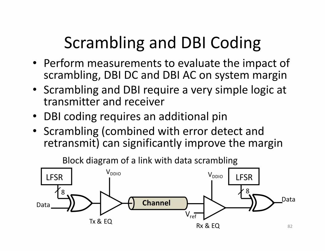
Scrambling and DBI Coding• Perform measurements to evaluate the impact of scrambling, DBI DC and DBI AC on system margin
• Scrambling and DBI require a very simple logic at transmitter and receiver
• DBI coding requires an additional pin• Scrambling (combined with error detect and retransmit) can significantly improve the margin
VDDIO
Vref
VDDIOLFSR LFSR8 8
DataData
Tx & EQ Rx & EQ
Channel
Block diagram of a link with data scrambling
82
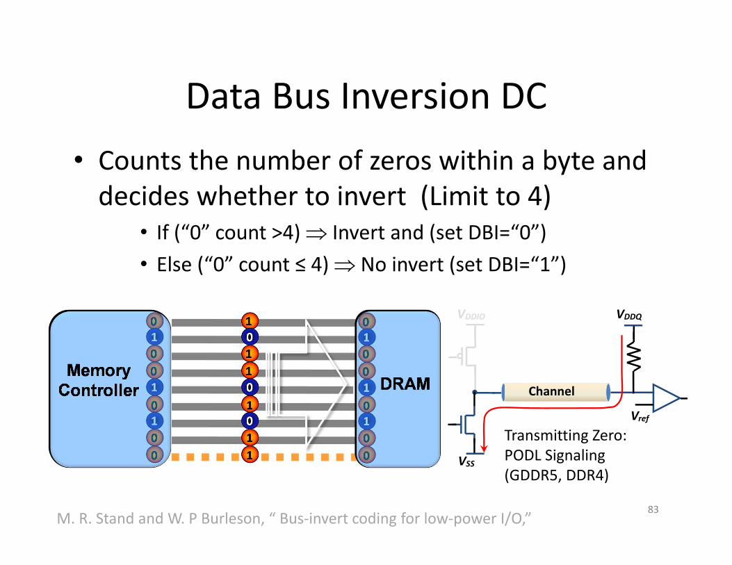
Data Bus Inversion DC• Counts the number of zeros within a byte and decides whether to invert (Limit to 4)
• If (“0” count >4) Invert and (set DBI=“0”)• Else (“0” count ≤ 4) No invert (set DBI=“1”)
83
Channel
VDDIO
Vref
VDDQ
VSS
Transmitting Zero: PODL Signaling(GDDR5, DDR4)
M. R. Stand and W. P Burleson, “ Bus‐invert coding for low‐power I/O,”
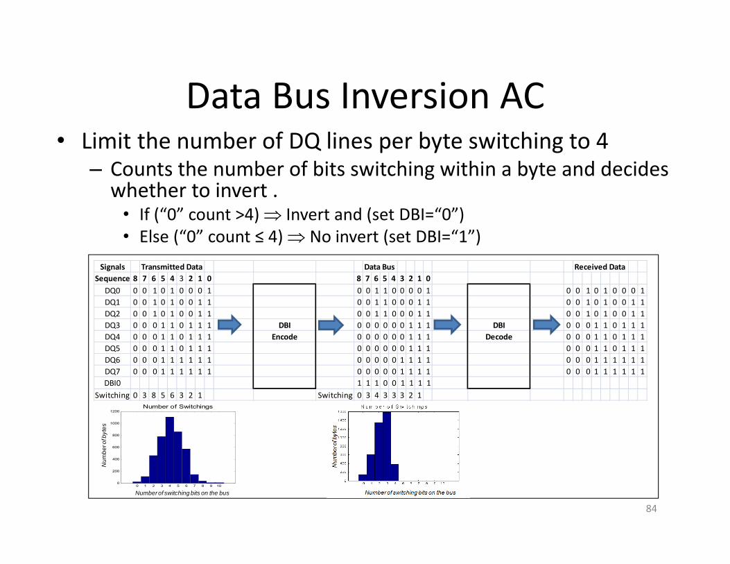
Data Bus Inversion AC• Limit the number of DQ lines per byte switching to 4
– Counts the number of bits switching within a byte and decides whether to invert .
• If (“0” count >4) Invert and (set DBI=“0”)• Else (“0” count ≤ 4) No invert (set DBI=“1”)
0 1 2 3 4 5 6 7 8 9 100
200
400
600
800
1000
1200Number of Switchings
Num
ber o
f byt
es
Number of switching bits on the bus
Signals Transmitted Data Data Bus Received DataSequence 8 7 6 5 4 3 2 1 0 8 7 6 5 4 3 2 1 0
DQ0 0 0 1 0 1 0 0 0 1 0 0 1 1 0 0 0 0 1 0 0 1 0 1 0 0 0 1DQ1 0 0 1 0 1 0 0 1 1 0 0 1 1 0 0 0 1 1 0 0 1 0 1 0 0 1 1DQ2 0 0 1 0 1 0 0 1 1 0 0 1 1 0 0 0 1 1 0 0 1 0 1 0 0 1 1DQ3 0 0 0 1 1 0 1 1 1 DBI 0 0 0 0 0 0 1 1 1 DBI 0 0 0 1 1 0 1 1 1DQ4 0 0 0 1 1 0 1 1 1 Encode 0 0 0 0 0 0 1 1 1 Decode 0 0 0 1 1 0 1 1 1DQ5 0 0 0 1 1 0 1 1 1 0 0 0 0 0 0 1 1 1 0 0 0 1 1 0 1 1 1DQ6 0 0 0 1 1 1 1 1 1 0 0 0 0 0 1 1 1 1 0 0 0 1 1 1 1 1 1DQ7 0 0 0 1 1 1 1 1 1 0 0 0 0 0 1 1 1 1 0 0 0 1 1 1 1 1 1DBI0 1 1 1 0 0 1 1 1 1
Switching 0 3 8 5 6 3 2 1 Switching 0 3 4 3 3 3 2 1
84