Embed Size (px)
Citation preview
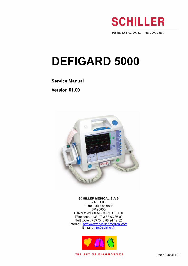
Part : 0-48-0065
SCHILLER MEDICAL S.A.SZAE SUD
4, rue Louis pasteurBP 90050
F-67162 WISSEMBOURG CEDEXTéléphone : +33 (0) 3 88 63 36 00Télécopie : +33 (0) 3 88 94 12 82
Internet : http://www.schiller-medical.comE.mail : [email protected]
DEFIGARD 5000Service Manual
Version 01.00
DEFIGARD 5000
0-48-0065 Page I June 2005
Revision historyof the service manual
Version 01.00 : June 2005
DEFIGARD 5000
0-48-0065 Page II June 2005
WARNING
This manual shall be considered to form an integral part of the devicedescribed.
This technical manual is intended for qualified personnel and describesthe operating, maintenance and troubleshooting procedures forDEFIGARD 5000.
Compliance with its content is a prerequisite for proper deviceperformance and for the safety of the patient and operator.
The manufacturer shall only be liable for the safety, reliability andperformance of the device if:
- assembly, extensions, adjustments, modifications or repairs areperformed by the manufacturer or by persons authorised by themanufacturer.
- the electrical installation of the facility of use complies with therequirements applicable in the country.
- the device is used in accordance with its instructions for use.
- the spare parts used are original parts from SCHILLER.
This manual describes the device at the time of printing.
The supply of this manual does not in any event constitute permissionor approval to modify or repair a device.
The manufacturer agrees to supply all the spare parts for a period often years.
All rights reserved for the devices, circuits, processes and namesappearing in this manual.
The DEFIGARD 5000 device shall be used as described in the User’sManual. The device may not be used for any purpose that has not beenspecifically described in the manual, as such use could be hazardous.
DEFIGARD 5000
0-48-0065 Page III June 2005
SAFETY INFORMATION
The product is marked as follows:
CE- 0459
in accordance with the requirements of Council Directive 93/42/EEC relating to medicalequipment, based on the essential requirements of annex I of the directive.
It fully meets the electromagnetic compatibility requirements of standard IEC 60601-1-2/EN60601-2 “Electromagnetic compatibility of medical electrical devices”.
The device has undergone interference suppression in accordance with the requirements ofstandard EN 50011, class B.
In order to optimise patient safety, electromagnetic compatibility, accurate measurementindication and proper device performance, users are advised to use only original spare partssupplied by SCHILLER. Any use of accessories other than original accessories shall be at theexclusive risk of the user. The manufacturer shall not be liable for any damage due to the use ofincompatible accessories or consumable supplies.
The manufacturer shall only be liable for the safety, reliability and performance of the device if:
- assembly, configuration, modifications, extensions or repairs are made by personnel fromSCHILLER MEDICAL or personnel duly authorised by SCHILLER MEDICAL.
- the device is used in accordance with its instructions for use.
Any use of the device other than as described in the instructions for use shall be made at theexclusive risk of the user.
This manual covers the device version and the safety standards applicable at the time ofprinting. All rights reserved for the circuits, processes, names, software and devices appearingin this manual.
The quality assurance system in use in the facilities of SCHILLER meets international standardsEN ISO 9001 and EN 46001.
Unless otherwise agreed in writing by SCHILLER, no part of the manufacturer’s literature may beduplicated or reproduced.
DEFIGARD 5000
0-48-0065 Page IV June 2005
Safety symbols used on the device
Danger! High voltage
Conventions used in the manual
Danger: indicates an imminent hazard which, if not avoided, will result in
death or serious injury to the user (and/or others).
Caution: Warning indicating conditions or actions that could lead to device
or software malfunctioning.
Note: Useful information for more effective and practical deviceoperation.
Additional information or explanation relating to the paragraphspreceding the note.
Manufacturer:
SCHILLERMEDICAL SA4, rue Louis Pasteur ZAE sudF- 67 162 Wissembourg
Tel. : **33 / (0) 3.88.63.36.00Fax : **33 / (0) 3.88.94.12.82
DEFIGARD 5000
0-48-0065 Page V June 2005
PRECAUTIONS WHILE TESTING THE DEVICE
While testing the DEFIGARD 5000 defibrillator, the patient may only be simulated with fixed high-voltage and high-power resistors that are well insulated from the ground or earth. Poorly insulateddevices or devices with loose contacts or devices containing components such as spark arresters orelectronic flash lamps may never be used as they could irremediably destroy the device..
DEFIGARD 5000
0-48-0065 Page VI June 2005
CONTENTS
1. Operation_________________________________________________________ 1-11.1. Display and controls._____________________________________________________ 1-11.2. Explanation of symbols used ______________________________________________ 1-31.3. Device operation. _______________________________________________________ 1-51.4. Technical specifications __________________________________________________ 1-9
2. Testing and maintenance ____________________________________________ 2-12.1. Functional testing _______________________________________________________ 2-12.2. Cleaning and disinfecting _________________________________________________ 2-1
3. Troubleshooting____________________________________________________ 3-14. Replacement of parts _______________________________________________ 4-1
4.1. Device disassembly procedure _____________________________________________ 4-24.2. Replacing the high-voltage capacitor ________________________________________ 4-44.3. Reassembling the device _________________________________________________ 4-54.4. Replacement of parts ____________________________________________________ 4-6
5. Technical description of boards________________________________________ 5-15.1. Overall description of the DEFIGARD 5000.___________________________________ 5-15.2. DEFI BOARD (part no. WSM0050A) ________________________________________ 5-25.3. CPU BOARD (part no. 3.2852) ____________________________________________ 5-315.4. POWER BOARD (part no. 3.2653)_________________________________________ 5-365.5. UPPER KEYPAD BOARD (part no. WSM0062A) _____________________________ 5-375.6. KEYPAD + BATTERY BOARD: (part no. WSM0060A) _________________________ 5-385.7. PACEMAKER BOARD: (part no. WSM0059A)________________________________ 5-39
6. Device modifications ________________________________________________ 6-16.1. Définition ______________________________________________________________ 6-16.2. DEFI BOARD __________________________________________________________ 6-16.3. CPU BOARD___________________________________________________________ 6-16.4. POWER BOARD________________________________________________________ 6-26.5. UPPER KEYPAD BOARD ________________________________________________ 6-26.6. KEYPAD + BATTERY BOARD _____________________________________________ 6-26.7. PACEMAKER BOARD ___________________________________________________ 6-2
7. Diagrams and layout drawings ________________________________________ 7-17.1. General synoptic ________________________________________________________ 7-17.2. DEFI BOARD (part no. WSM0050A) ________________________________________ 7-37.3. CPU BOARD (part no. 3.2852) _____________________________________________ 7-67.4. POWER BOARD (part no. 3.2653)__________________________________________ 7-97.5. UPPER KEYPAD BOARD (part no. WSM0062A) _____________________________ 7-117.6. KEYPAD + BATTERY BOARD: (part no. WSM0060A) _________________________ 7-137.7. PACEMAKER BOARD: (part no. WSM0059A)________________________________ 7-157.8. LCD DISPLAY TFT 800X600 : (part no. 4-30-0001) ___________________________ 7-187.9. LIGHTING BOARD: (part no. 4-24-0003) ____________________________________ 7-19
Operation
0-48-0065 Page 1-1 June 2005
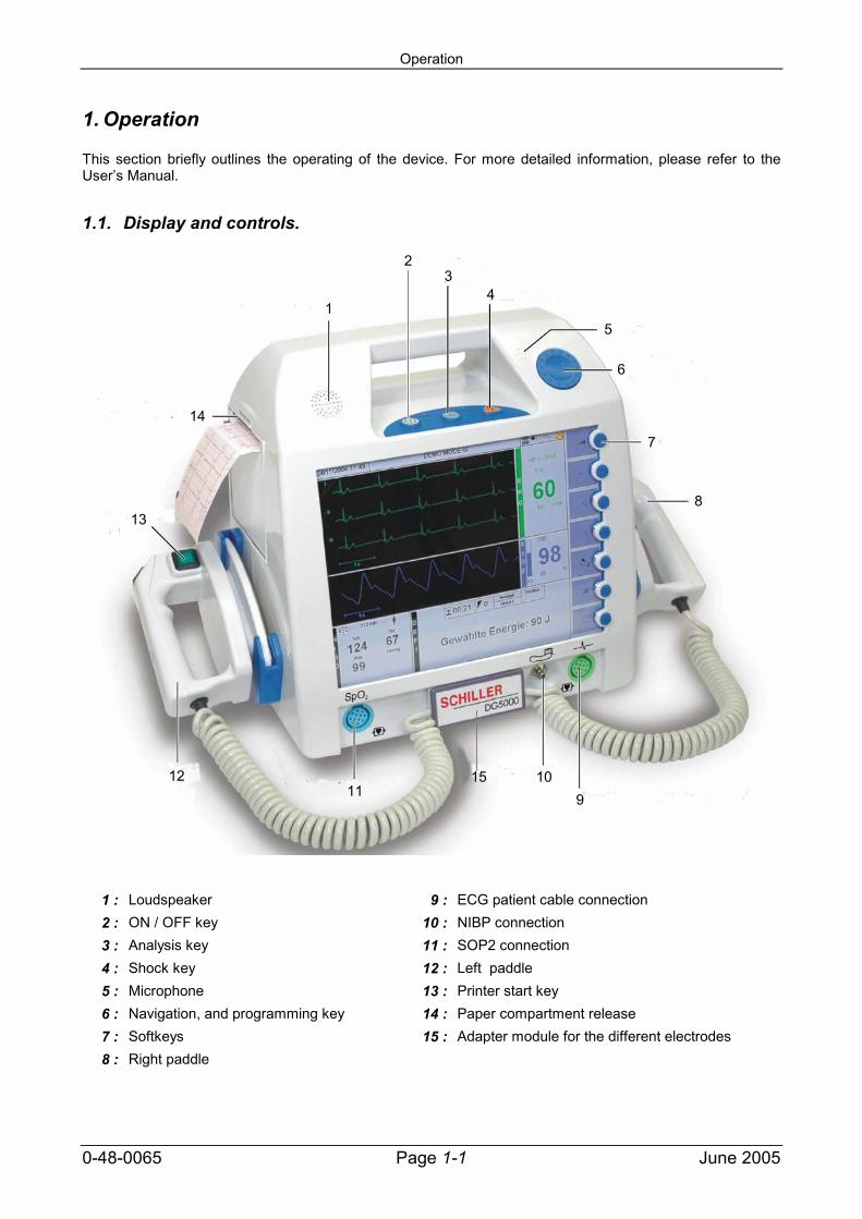
1. Operation
This section briefly outlines the operating of the device. For more detailed information, please refer to theUser’s Manual.
1.1. Display and controls.
1 : Loudspeaker 9 : ECG patient cable connection2 : ON / OFF key 10 : NIBP connection3 : Analysis key 11 : SOP2 connection4 : Shock key 12 : Left paddle5 : Microphone 13 : Printer start key6 : Navigation, and programming key 14 : Paper compartment release7 : Softkeys 15 : Adapter module for the different electrodes8 : Right paddle
1
23
4
5
6
7
8
910
1112
13
14
15
Operation
0-48-0065 Page 1-2 June 2005
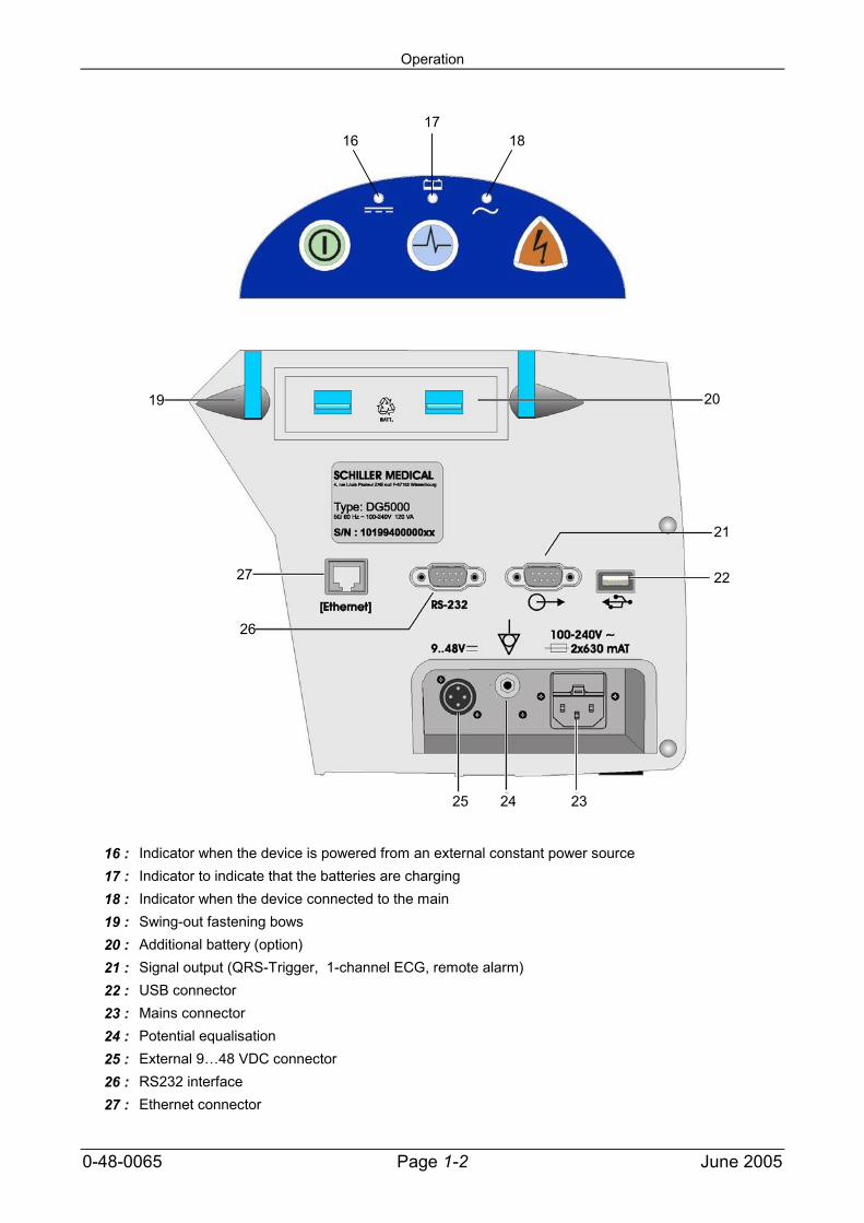
16 : Indicator when the device is powered from an external constant power source17 : Indicator to indicate that the batteries are charging18 : Indicator when the device connected to the main19 : Swing-out fastening bows20 : Additional battery (option)21 : Signal output (QRS-Trigger, 1-channel ECG, remote alarm)22 : USB connector23 : Mains connector24 : Potential equalisation25 : External 9…48 VDC connector26 : RS232 interface27 : Ethernet connector
1617
18
19 20
21
22
23
26
25 24
27
Operation
0-48-0065 Page 1-3 June 2005
1.2. Explanation of symbols used
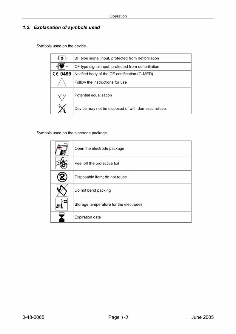
Symbols used on the device.
BF type signal input, protected from defibrillation
CF type signal input, protected from defibrillation
Notified body of the CE certification (G-MED)
Follow the instructions for use
Potential equalisation
Device may not be disposed of with domestic refuse.
Symbols used on the electrode package.
Open the electrode package
Peel off the protective foil
Disposable item; do not reuse
Do not bend packing
Storage temperature for the electrodes
Expiration date
Operation
0-48-0065 Page 1-4 June 2005
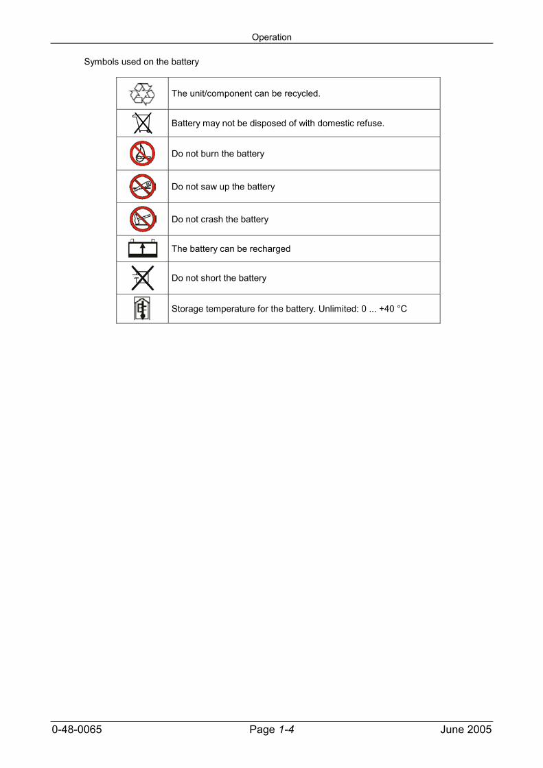
Symbols used on the battery
The unit/component can be recycled.
Battery may not be disposed of with domestic refuse.
Do not burn the battery
Do not saw up the battery
Do not crash the battery
The battery can be recharged
Do not short the battery
Storage temperature for the battery. Unlimited: 0 ... +40 °C
Operation
0-48-0065 Page 1-5 June 2005
1.3. Device operation.
DEFIGARD 5000 is a monitor/defibrillator designed for in-hospital use. It is started up by keeping the On/Offkey on the upper keypad pressed down for two seconds or more.
Power supply:The device is powered by the mains, a battery (lithium ion battery only) or an external 9 - 48 VDC powersupply. It has a fixed battery in the lower slot, which can be charged from the mains or the external VDCpower supply. The capacity of the battery is sufficient for:
- 70 shocks at the maximum energy or- 2 hours of monitor operation.
A second removable battery (optional) may be inserted in the upper slot to double the life.
Defibrillation:DEFIGARD 5000 is a defibrillator that uses pulse biphasic waveforms - Multipulse Biowave®.The device offers two operating modes, the semiautomatic mode, called SAD, and the manual mode. Thesetwo operating modes depend on the type of defibrillation cartridge inserted. There are three types of cartridge- adhesive electrode cartridge, internal electrode cartridge and handheld paddle electrode cartridge. Awindow on the screen indicates the defibrillator settings.
Possibilities offered by the defibrillator:- Manual defibrillation with adhesive electrodesFor manual defibrillation with adhesive electrodes, you need to use the cartridge for adhesive electrodes. Thecharge and energy selection buttons are located on the side keypad, whilst the shock button is located on theupper keypad.- Semiautomatic defibrillation with adhesive electrodesThe same cartridge is used with adhesive electrodes. The device must offer the semiautomatic function.Adhesive electrodes are available for children and adults. The device recognises the type of electrode appliedand selects the defibrillation energy levels accordingly. The control buttons for analysing and shock deliveryare located on the upper keypad.- Internal manual defibrillation (optional)Use the cartridge that offers the facility to use the internal defibrillation paddles. The charge and energyselection buttons are on the side keypad. The shock button is located on the upper keypad.- Manual defibrillation with handheld electrodes (optional)Use the handheld electrode cartridge. The charge/shock button and the energy selection button can be foundon the electrodes.
Semiautomatic mode:In the SAD mode, the user takes action on the basis of the messages sent by the system (in accordance withAHA/ERC protocols).At any time (except during CPR), if an electrode fault is detected, the AHA/ERC protocol is stopped. It isresumed when the fault disappears.During the analysis (which is set off by pressing the Analyse key), if a loose contact is detected, the analysisis interrupted throughout the duration of the fault. It is automatically resumed when the fault disappears.After an initial analysis, if the analysed ECG signal is too weak, a message asks the user to apply CPR(cardiac pulmonary resuscitation) for one minute. The display lasts during that time, when pressing theAnalyse key starts off the analysis cycle.After an initial analysis, if there is noise in the ECG signal, a message is displayed for one minute to ask theuser to apply CPR (cardiopulmonary resuscitation). The display lasts during that time, when pressing theAnalyse key starts off the analysis cycle.
Operation
0-48-0065 Page 1-6 June 2005
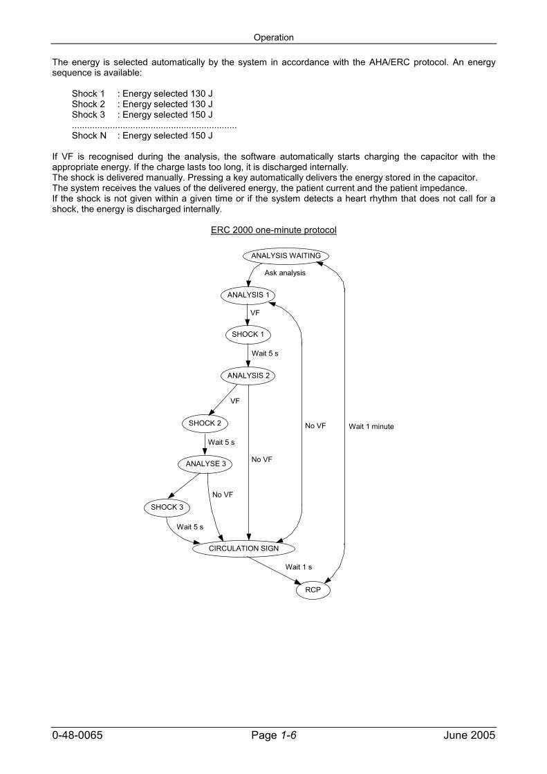
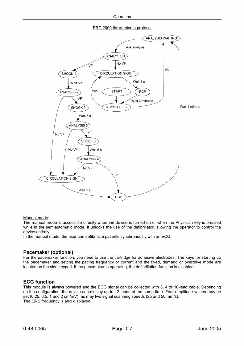
The energy is selected automatically by the system in accordance with the AHA/ERC protocol. An energysequence is available:
Shock 1 : Energy selected 130 JShock 2 : Energy selected 130 JShock 3 : Energy selected 150 J.................................................................Shock N : Energy selected 150 J
If VF is recognised during the analysis, the software automatically starts charging the capacitor with theappropriate energy. If the charge lasts too long, it is discharged internally.The shock is delivered manually. Pressing a key automatically delivers the energy stored in the capacitor.The system receives the values of the delivered energy, the patient current and the patient impedance.If the shock is not given within a given time or if the system detects a heart rhythm that does not call for ashock, the energy is discharged internally.
ERC 2000 one-minute protocol
Wait 1 minute
Ask analysis
ANALYSIS WAITING
ANALYSIS 1
SHOCK 1
CIRCULATION SIGN
RCP
Wait 1 s
Wait 5 s
No VF
Wait 5 s
VF
No VF
No VF
Wait 5 s
VF
ANALYSIS 2
ANALYSE 3
SHOCK 2
SHOCK 3
Operation
0-48-0065 Page 1-7 June 2005
ERC 2000 three-minute protocol
Wait 3 minutes
Ask analysis
ANALYSIS WAITING
ANALYSIS 1
CIRCULATION SIGN
RCP
Wait 1 s
Wait 5 s
VF
No VF
No VF
Wait 5 s
VF
ANALYSIS 2
ANALYSiS 3
RCP
CIRCULATION SIGN
START
ASYSTOLIE ?
Yes
Wait 1 s
ANALYSiS 4
VF
Wait 5 s
No VF
No VF
NoVF
Wait 1 minute
SHOCK 1
SHOCK 2
SHOCK 3
Manual mode:The manual mode is accessible directly when the device is turned on or when the Physician key is pressedwhile in the semiautomatic mode. It unlocks the use of the defibrillator, allowing the operator to control thedevice entirely.In the manual mode, the user can defibrillate patients synchronously with an ECG.
Pacemaker (optional)For the pacemaker function, you need to use the cartridge for adhesive electrodes. The keys for starting upthe pacemaker and setting the pacing frequency or current and the fixed, demand or overdrive mode arelocated on the side keypad. If the pacemaker is operating, the defibrillation function is disabled.
ECG functionThis module is always powered and the ECG signal can be collected with 3, 4 or 10-lead cable. Dependingon the configuration, the device can display up to 12 leads at the same time. Four amplitude values may beset (0.25, 0.5, 1 and 2 cm/mV), as may two signal scanning speeds (25 and 50 mm/s).The QRS frequency is also displayed.
Operation
0-48-0065 Page 1-8 June 2005
SPO2 function (optional)The window of this function is only displayed on the screen when the SPO2 connector is detected by thedevice. The window displays the SPO2 curve and the saturation rate.When the screen displays the 12 leads of the ECG, the SPO2 curves disappears, but the saturation rateremains displayed.
NIBP function (optional)The NIBP may be set to Adult or Infant. For each configuration, you can take manual, continuous or cyclicalmeasurements.The Sys, Dia and MAP values are displayed on the screen.
Memory functionThe ECG curve and the trends are saved in a compact flash memory in the device.
Data transmission function- A connection for GSM or standard modems is provided for transmitting the 12-lead ECG- A USB connector is provided for retrieving data from the device- An Ethernet link for upgrading softwareAll the connectors are located at the rear of the device.
Recorder function (optional)The recorder can print ECG, SPO2 or trend curves.
Operation
0-48-0065 Page 1-9 June 2005
1.4. Technical specifications
Manufacturer : SCHILLER MEDICAL
Device type : DEFIGARD 5000
Dimensions : 289 x 271 x 177 mm (height x width x depth)
Weight : 5,3 kg
Protection case : IPX 1
Power supplyVoltage : 100 - 240 VAC, 50/60HzPower consumption : 120 VABattery operation : Up to 2 hours, option with additional battery up to 4 hours.Fuses : 2 x 200 mAT at 250 VAC, 2 x 315 mAT at 115 VACExternal power supply : 9 - 48 VDC max. 2,5 A
: The unit is suitable for use in networks according to IEC 60601-1-2
BatteriyBattery type : Lithium / ion 10,8 V 4,3 A.Autonomy : 70 schocks with maximum energy or 4 hours of monitoring (alternately 30
min on, 30 min off).
Environmental conditionsTransport / storage : Temperature -10 to + 50 °C
: Relative humidity 0 to 95 %, no condensation: Atmospheric pressure 700 à 1060 hPa
Operating : Temperature 0 à + 40 °C: Relative humidity 30 à 95 %, no condensation: Atmospheric pressure 500 à 1060 hPa
DisplayType : High resolution colour LCD (800 X 600) with backlightDimensions : 214 mm x 158,4 mm (10,4")
PrinterResolution : 8 dots / mm (amplitude-axis), 40 dots / mm (time-axis) at 25 mm / sPaper : Thermoreactive, Z-foldet, 72 mm width, length approx. 20 m.Print speed : 25, 50 mm / sRecording tracks : 3-channel display, with optimal width of 72 mm.
Connections : ECG patient cable, SPO2, PNI.
Interfaces : RS-232: Analogue for QRS trigger, 1-chanel ECG and remote alarm: USB: Ethernet
Défibrillation pulse form- Biphasic pulsed defibrillation impulse with fixed physiological optimum phase durations.- Near stabilisation of the emitted energy in function with the patient resistance us ing pulse-pause
modulation depending on the measured patient resistance.
Operation
0-48-0065 Page 1-10 June 2005
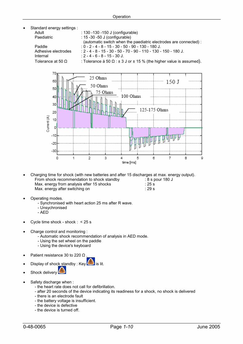
Standard energy settings :Adult : 130 -130 -150 J (configurable)Paediatric : 15 -30 -50 J (configurable)
(automatic switch when the paediatric electrodes are connected) :Paddle : 0 - 2 - 4 - 8 - 15 - 30 - 50 - 90 - 130 - 180 J.Adhesive electrodes : 2 - 4 - 8 - 15 - 30 - 50 - 70 - 90 - 110 - 130 - 150 - 180 J.Internal : 2 - 4 - 6 - 8 - 15 - 30 J.Tolerance at 50 Ω : Tolerance à 50 Ω : ± 3 J or ± 15 % (the higher value is assumed).
Charging time for shock (with new batteries and after 15 discharges at max. energy output).From shock recommendation to shock standby : 8 s pour 180 JMax. energy from analysis efter 15 shocks : 25 sMax. energy after switching on : 29 s
Operating modes.- Synchronised with heart action 25 ms after R wave.- Unsychronised- AED
Cycle time shock - shock : < 25 s
Charge control and monitoring :- Automatic shock recommendation of analysis in AED mode.- Using the set wheel on the paddle- Using the device's keyboard
Patient resistance 30 to 220 Ω .
Display of shock standby : Key is lit.
Shock delivery
Safety discharge when :- the heart rate does not call for defibrillation.- after 20 seconds of the device indicating its readiness for a shock, no shock is delivered- there is an electrode fault- the battery voltage is insufficient.- the device is defective- the device is turned off.
Operation
0-48-0065 Page 1-11 June 2005
Shock delivery.- Via applied disposable adhesive defibrillation electrodes.- Via paddles.- Via spoons
Defibrillation electrode connection.External defibrillation : Type BF.Internal defibrillation : Type CF.
Defibrillation electrodes:- Adult electrode : 78 cm2 de surface active- Paediatric electrode : 28 cm2 de surface active- Electrode cable length : 2 m
VF/VT detection :- Shock recommendation : in case of VF and VT (VT > 180 p/min)- Sensitivity : 98.43 %
Specificity: 99.8 %. These values have been found with the AHA database, which contains casesof VF and VT with and without artefacts..
- Conditions required for ECG analysis :Minimum amplitude for the signals used > 0.15 mV , signals of < 0.15 mV are considered to showasystole
- Definition :Sensitivity: Correct detection of heart rates for which defibrillation shocks are recommended.Specificity: Correct detection of heart rates for which defibrillation shocks are not recommended.
ECG :Leads : Simultaneous, synchronous recording 12 leadsPatient cable : 3-,4-, 10-lead cable, type CFHeart rate : 30 – 300 beats/minLead display : Selection of 1 to 12 simultaneous leadsBand pass : 0.5...35 Hz or 0.05...150 Hz (depending on the ECG source)
NIBP - non-invasive blood pressure :Measurement : Automatic or manualMeasuring method : OscillometricConnection : Type CFMeasurement range :Adults : Sys 30...255 mmHg, dia 15...220 mmHgNeonates : Sys 30...135 mmHg, dia 15...110 mmHgAccuracy : ± 3 mmHg et ± 2 B/min
SPO2 (pulsoximetry) :Amplifier : MasimoUsing the Monitor : Normal and sensitiveAccuracy : - SPO2
Adults 1…100% ± 2 Neonates 70…100% ± 3 - PP 25 …240/min ± 4
Calibration range : 70…100%Connection : Type CFMeasurement range : SPO2 1…100%
: PP 25 …240/minDisplayed range : 1…100%
SavingECG : 1 hourEvents : 500
Testing and maintenance
0-48-0065 Page 2-1 June 2005
2. Testing and maintenanceThis section describes the test and maintenance procedures recommended with DEFIGARD 5000.
2.1. Functional testing
The device runs an automatic test every time is switched on. The test lasts less than 5 seconds and consistsin checking all the hardware functions. If a blocking error is found, an error message is displayed on thescreen and a sound alarm is emitted till the device is switched off by the operator (by pressing the Off key).The device is blocked and goes off automatically after five minutes.
The device can run a periodic automatic test at a configurable frequency. That automatic test may be daily,weekly or user-defined by indicating the number of days between two tests (1 to 30 days). A key forimmediately starting up the test is available as well. During the self test, all the hardware functions and thebattery charge status are tested. No information is displayed on the screen during the test. The test result issaved and can be retrieved subsequently. The last 30 tests are saved.If the tests do not show any error, the system goes off automatically.If, on the other hand, a serious error is found, a sound alarm is emitted for 10 seconds every 2 minutes till thedevice is switched on again. At that time, the error is displayed on the screen. The device is blocked.A selection is available to restart all the tests.If the tests do not show any error, the system starts up nominal operation.If, on the other hand, a blocking error is found, the error is displayed on the screen and a sound alarm isemitted till the device is switched off by the operator (by pressing Off). The device is blocked.
2.2. Cleaning and disinfecting
Caution: Switch the device off before cleaning it. Remove the cellbefore you start cleaning the device in order to eliminate therisk of the device starting up accidentally. Also disconnectthe defibrillation electrodes of the device before cleaning.
No liquid shall be allowed to enter into the device. However,if that does happen, the device may not be used before it isverified by the after-sales service department.
The device or electrodes may never be cleaned with substances such as ether, acetone, esters,aromatic chemicals etc.Never use phenol-based cleaners or cleaners containing peroxide derivatives to disinfect thesurfaces of the housing of the device. Dispose of all single-use electrodes immediately after use in order to eliminate the risk of
accidental reuse (disposal with hospital waste). Before cleaning the electrode cables of sensors, disconnect them from the device. For cleaning
and disinfecting, wipe the cables with a gauze cloth moistened with cleaner or disinfectant.Never immerse the connectors in liquid. The cleaning solution used may be any cleaning ordisinfecting solution that is commonly used in hospitals.
Proceed likewise with the device housing, with a cloth moistened with cleaner or disinfectant. Noliquid may be allowed to penetrate into the device during the operation.

Troubleshooting
0-48-0065 Page 3-1 June 2005
3. Troubleshooting
This section addresses the troubleshooting procedures for DEFIGARD 5000. If you have trouble locating orcorrecting the problem, contact the after-sales service department of SCHILLER.
Note: If an error message is displayed before you call in a Schillertechnician, note the error number and restart the device to checkthat the reason for the problem is not merely a program crash.
Precautions during troubleshooting
While testing the DEFIGARD 5000 defibrillator, the patient may only be simulated with fixed high-voltage and high-power resistors that are well insulated from the ground or earth. Poorly insulateddevices or devices with loose contacts or devices containing components such as spark arresters orelectronic flash lamps may never be used as they could irremediably destroy the device.
Danger: Before any work on an open device, you need to IMPERATIVELY
CHECK IF THE HV CAPACITOR IS PROPERLY DISCHARGED.
ERROR FINDING POSSIBLE CAUSES CORRECTIVE ACTION
ERROR MESSAGES
Board error(in the ECG window)
1. CPU board problem 1. Replace the CPU board
Board error(in the SPO2 window)
1. SPO2 board problem 1. Replace the SPO2 board
Board error(in the NIBP window)
1. NIBP board problem 1. Replace the NIBP board
Analogue board 1. CPU board fault 1. Replace the CPU boardPower board error 1. POWER board fault 1. Replace the POWER boardVF error 1. CPU board fault 1. Replace the CPU boardNIBP error 1. NIBP module fault 1. Replace the NIBP board
DEFIBRILLATOR ERROR MESSAGES
Board error(in DEFI window)
1. DEFI board problem 1. Replace the DEFI board
PROCESSOR ERROR 1. DEFI board fault 1. Replace the DEFI boardPROGRAM ERROR 1. Program problem with
DEFI board1. Reload the program
ERROR DETECTION CIRCUIT ERROR 1. DEFI board fault 1. Replace the DEFI boardSELECTED ENERGYVOLTAGE REFERENCE ERROR
1. DEFI board fault 1. Replace the DEFI board
ADC CONVERTER ERROR 1. DEFI board fault 1. Replace the DEFI boardCHARGE TRANSISTOR ERROR 1. DEFI board fault 1. Replace the DEFI boardDISCHARGE TRANSISTOR ERROR 1. DEFI board fault 1. Replace the DEFI boardCOMPENSATION EPROM ERROR 1. DEFI board fault 1. Replace the DEFI boardSHOCK BUTTON ERROR 1. Problem with handheld
paddle cartridge2. UPPER KEYPAD boardfault
1. Replace the cartridge
2. Replace the UPPERKEYPAD board
Replacement of parts
0-48-0065 Page 4-1 June 2005
4. Replacement of partsThis section addresses the issue of how to dismantle DEFIGARD 5000 in order to replace faulty parts. Thewarnings below apply to all work inside the device.
Warning: The DEFIGARD 5000 is a defibrillator with a high-voltagecapacitor that can be charged to a fatal voltage. The devicemay only be dismantled by specially authorised and trainedpersonnel.
Before any work on an open device, you need toIMPERATIVELY CHECK IF THE HV CAPACITOR IS PROPERLYDISCHARGED.
Caution: Before dismantling the device, remove the battery or the cellfrom its slot.
Caution: The device contains circuits sensitive to electrostaticdischarge. All work on the DEFIGARD 5000 device shall beperformed in accordance with ESD rules. The repairs shall beperformed on an antistatic mat connected to the earth and theoperator shall wear an antistatic strap also connected to themat. In the event of any work on the high-voltage part of thedefibrillator, remove the antistatic strap.
Caution: A general device test shall be performed each time the deviceis opened.
Replacement of parts
0-48-0065 Page 4-2 June 2005
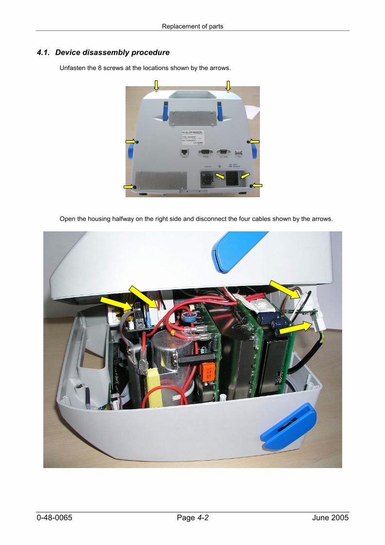
4.1. Device disassembly procedure
Unfasten the 8 screws at the locations shown by the arrows.
Open the housing halfway on the right side and disconnect the four cables shown by the arrows.
Replacement of parts
0-48-0065 Page 4-3 June 2005
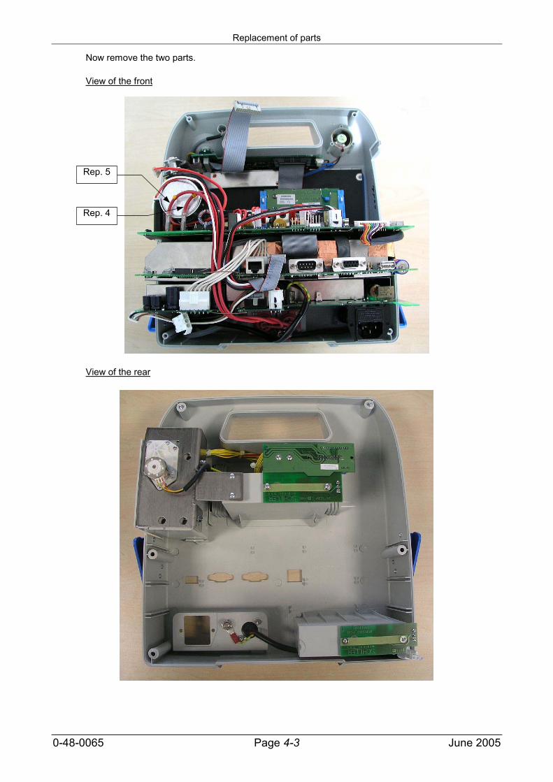
Now remove the two parts.
View of the front
View of the rear
Rep. 5
Rep. 4
Replacement of parts
0-48-0065 Page 4-4 June 2005
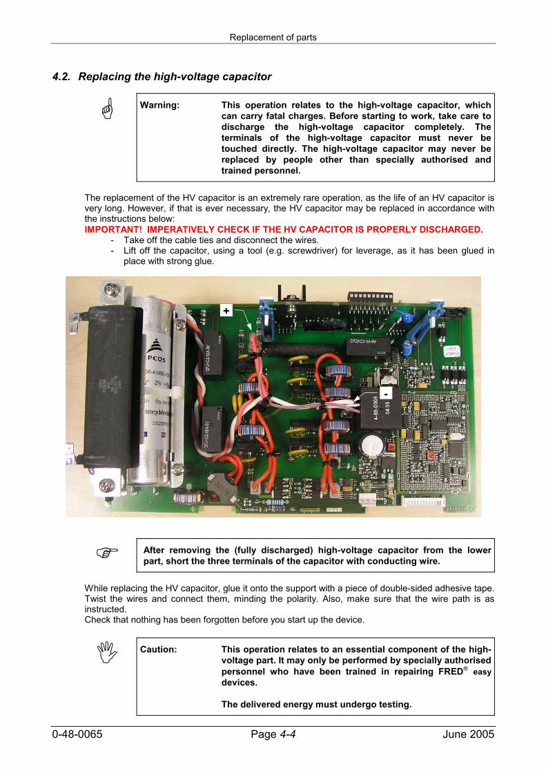
4.2. Replacing the high-voltage capacitor
Warning: This operation relates to the high-voltage capacitor, whichcan carry fatal charges. Before starting to work, take care todischarge the high-voltage capacitor completely. Theterminals of the high-voltage capacitor must never betouched directly. The high-voltage capacitor may never bereplaced by people other than specially authorised andtrained personnel.
The replacement of the HV capacitor is an extremely rare operation, as the life of an HV capacitor isvery long. However, if that is ever necessary, the HV capacitor may be replaced in accordance withthe instructions below:IMPORTANT! IMPERATIVELY CHECK IF THE HV CAPACITOR IS PROPERLY DISCHARGED.
- Take off the cable ties and disconnect the wires.- Lift off the capacitor, using a tool (e.g. screwdriver) for leverage, as it has been glued in
place with strong glue.
After removing the (fully discharged) high-voltage capacitor from the lowerpart, short the three terminals of the capacitor with conducting wire.
While replacing the HV capacitor, glue it onto the support with a piece of double-sided adhesive tape.Twist the wires and connect them, minding the polarity. Also, make sure that the wire path is asinstructed.Check that nothing has been forgotten before you start up the device.
Caution: This operation relates to an essential component of the high-voltage part. It may only be performed by specially authorisedpersonnel who have been trained in repairing FRED easydevices.
The delivered energy must undergo testing.
-
+
Replacement of parts
0-48-0065 Page 4-5 June 2005
4.3. Reassembling the device
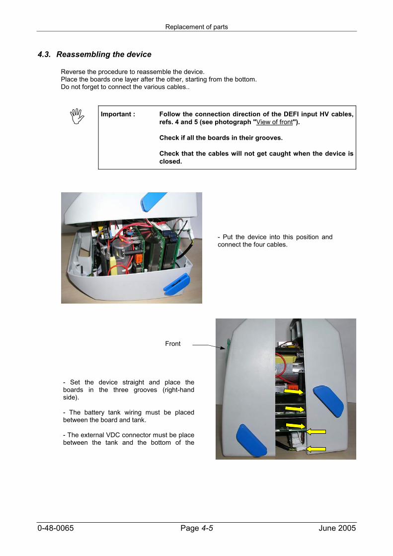
Reverse the procedure to reassemble the device.Place the boards one layer after the other, starting from the bottom.Do not forget to connect the various cables..
Important : Follow the connection direction of the DEFI input HV cables,refs. 4 and 5 (see photograph "View of front").
Check if all the boards in their grooves.
Check that the cables will not get caught when the device isclosed.
- Put the device into this position andconnect the four cables.
- Set the device straight and place theboards in the three grooves (right-handside).
- The battery tank wiring must be placedbetween the board and tank.
- The external VDC connector must be placebetween the tank and the bottom of the
Front
Replacement of parts
0-48-0065 Page 4-6 June 2005
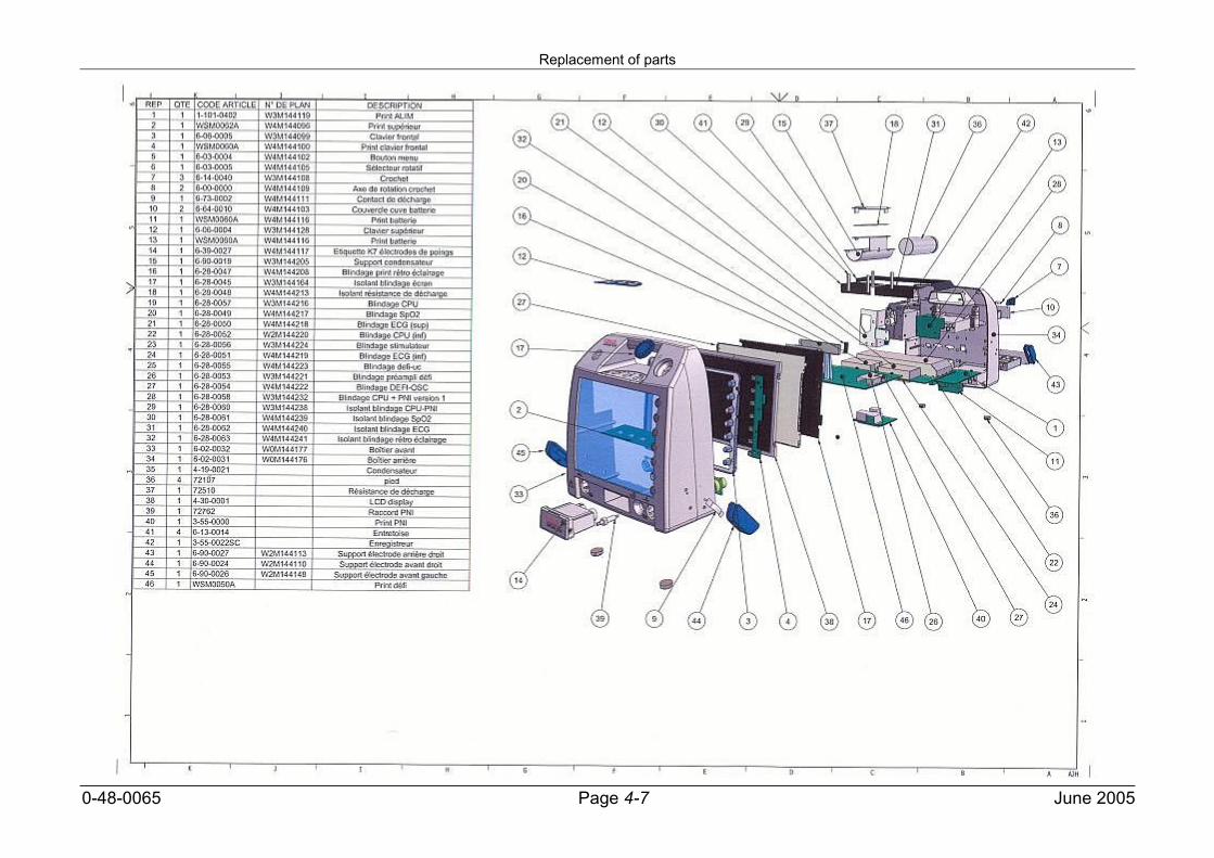
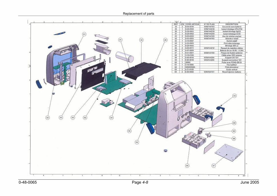
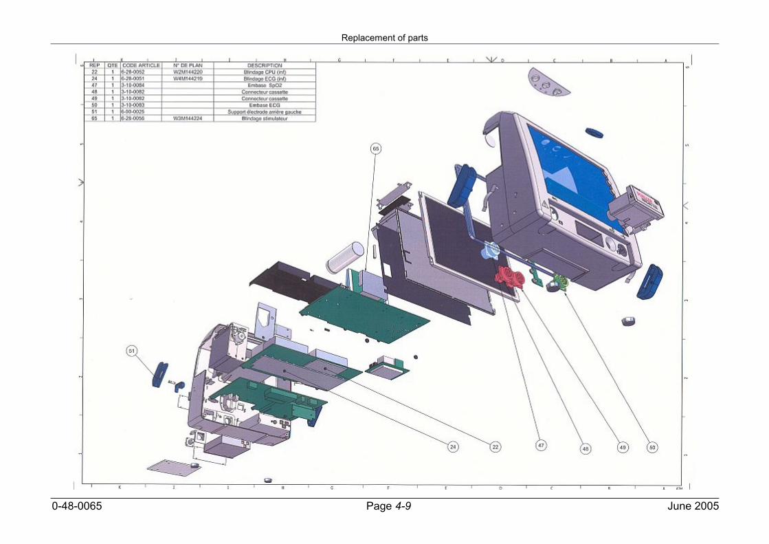
4.4. Replacement of parts
Warning: Parts may only be replaced by personnel who have beenspecially trained and authorised by SCHILLER.
Besides, the replacement parts shall be original SCHILLERparts.
Note: To order a new part from SCHILLER, provide the part number and theserial number of the device located under the device. After that, specifythe item code of the part..
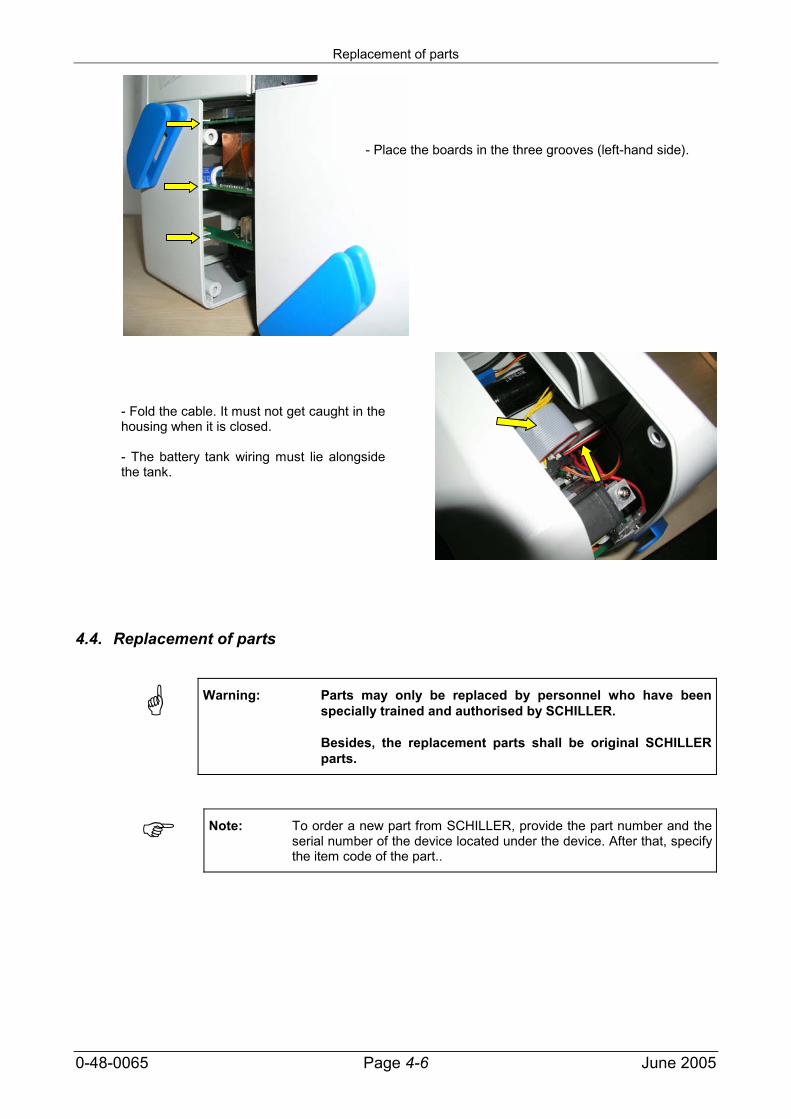
- Fold the cable. It must not get caught in thehousing when it is closed.
- The battery tank wiring must lie alongsidethe tank.
- Place the boards in the three grooves (left-hand side).
Replacement of parts
0-48-0065 Page 4-7 June 2005
Replacement of parts
0-48-0065 Page 4-8 June 2005
Replacement of parts
0-48-0065 Page 4-9 June 2005
Technical description of boards
0-48-0065 Page 5-1 June 2005
5. Technical description of boards
5.1. Overall description of the DEFIGARD 5000.
Overview of DEFIGARD 5000 :
DEFIGARD 5000 is made up of the following subassemblies:
The DEFI board, which contains the various digital processing functions specific to the defibrillator,the analogue processing functions and the high-voltage circuit of the defibrillator. The board may alsohave an (optional) PACEMAKER board.
The CPU board, which contains the various digital processing, analogue processing and savingfunctions. It may also have (optional) SPO2 and NIBP boards.
The POWER board, which supplies the power required for all the functions.
Two KEYPAD boards that act as the interface between the user and the device.
Two BATTERY boards that act as the interface between the batteries and the device.
An LCD SCREEN with a BACKLIGHTING board that acts as the visual interface betweenDEFIGARD 5000 and the user.
Technical description of boards
0-48-0065 5-2 June 2005
5.2. DEFI BOARD (part no. WSM0050A)
5.2.1. DEFIBRILLATOR PCB
The Defibrillator PCB (part no. WSM 0050_PCB) includes the various parts below: ECG preamplifier
The ECG preamp part acquires the ECG signal collected through the defibrillation electrodes andmeasures the contact impedance.
Input interface circuitThe input interface circuit part acts as the interface between the various defibrillation cartridges and thedefibrillator control circuit.
Defibrillator control circuitThe defibrillator control circuit part controls the charging and discharging of the HV capacitor throughthe electrode cartridges or the keys on the front of the device.
High-voltage circuit and HV capacitorThe high-voltage circuit charges and discharges the HV capacitor and measures the charging voltageand the patient current during the defibrillation shock.
IGBT control circuitThe IGBT control circuit controls the IGBTs of the high-voltage unit in order to generate a pulsebiphasic waveform with patient impedance compensation.
Fault detection circuitThe fault detection circuit monitors the critical components in order to detect any fault.
5.2.2. FUNCTIONING OF THE DEFIBRILLATOR PART
The explanation of the working of the defibrillator part refers to chart DG 5000 Defibrillator..
5.2.2.1. OVERALL DESCRIPTION
The defibrillator circuit has seven connectors: connector JP1 (3 contacts) for powering the defibrillator circuit connector JP2 (20 contacts) for connecting with the CPU board and the front connectors JP3 & JP4 (high-voltage contacts) connected to the HV cables of the defibrillator electrode
base connector JP7 (10 contacts) connected to the floating part of the 10-channel ECG preamplifier two connectors JP3 (14 contacts) connected to the LV cables of the defibrillator electrode base
The power circuit of the defibrillator part, which charges the HV capacitor, is directly powered by DC voltagewith a protective fuse (voltage DC_FUSED). The defibrillator control circuits, the IGBT control circuits and thefault detection circuit is powered by +5 V generated on the defibrillator board from the +12 V voltage. TheECG preamplifier circuit is powered from the power supplied by the 10-channel ECG preamplifier viaconnector JP7. The voltage references used by the defibrillator part are generated locally on the defibrillatorcircuit.
Technical description of boards
0-48-0065 5-3 June 2005
The defibrillator function of DG 5000 is a sequential circuit with six distinct phases:
1) Standby phase: Phase where DG5000 is on (monitoring function); the defibrillator part isstanding by (no demand for a charge).
2) Charge phase: Phase during which the HV generator charges the HV capacitor (40 µF /3.1 kV). The charge phase in the semiautomatic mode may be initiated bytwo different controls:
1. Pre-charge control2. Charge control
3) Pre-charge completed: Phase that follows initiation by the pre-charge control (in semiautomaticmode), when the selected energy has been reached. After pre-charging iscompleted, the delivery of the defibrillation shock is not allowed.
4) Hold phase: Phase that follows initiation by the charge control, when the selectedenergy is reached. This phase lasts for no more than 20 seconds, whenthe HV capacitor remains charged. DG5000 is ready to deliver adefibrillation shock.
5) Shock phase: This is the phase where DG5000 delivers the pulse biphasic defibrillationshock with patient impedance.
6) Safety discharge: This is the phase where the energy stored in the HV capacitor is deliveredinto a safety discharge circuit of DG5000.
5.2.2.2. ECG PREAMPLIFIER
The preamplifier part carries out the following functions: Powering the floating defibrillator ECG part Acquisition of the ECG signal Amplification and processing of the ECG signal Verification of the acquisition chain Patient impedance measurement Transmission of QRS pulses from the 10-channel ECG preamplifier
OVERALL DESCRIPTION:On the defibrillator PCB, the floating part of the defibrillation ECG preamplifier is located under the two metalshields that occupy the space under the high-voltage capacitor.The floating power of the defibrillation ECG preamplifier is provided through transformer TR3 from thevoltages supplied by the 10-channel ECG preamplifier. The defibrillator ECG preamplifier part amplifies theECG signal and measures the patient impedance sent by the defibrillation electrodes (handheld paddles oradhesive electrodes).The amplified ECG signal and the patient impedance signal are sent by an optocoupler to the floating ECGpart of the 10-channel ECG preamplifier. The signals are transmitted by cyclic ratio modulation. The 10-channel ECG preamplifier therefore receives two possible sources of ECG signals: the ECG signal throughthe patient cable and the ECG signal through the defibrillation electrodes.The 10-channel ECG preamplifier directly controls the defibrillator ECG preamplifier if pacemaker pulses aredetected (signal INH_PACE). The test of the ECG signal acquisition chain by the defibrillation electrodes isalso controlled by the 10-channel ECG preamplifier board during the self test of DG5000 (10 Hz signal). TheQRS signal detected and formed by the 10-channel ECG preamplifier is sent by an optocoupler to thedefibrillator control circuit in order to control working during cardioversion (signal –QRSTRIG_DEF).The defibrillator ECG preamplifier part measures the patient impedance through a 30 kHz sine-wave signal.After processing, the signal with the patient impedance value is sent to the 10-channel ECG preamplifier. Thedefibrillator ECG preamplifier circuit has a window comparator where the output signal is used by thedefibrillator control circuit in order to authorise the defibrillation shock only if the defibrillation electrodes areglued correctly (signal –PIMP_DEF).
Technical description of boards
0-48-0065 5-4 June 2005
ECG PREAMPLIFIER AMPLIFICATION:The power supply for the floating part of the ECG preamplifier is generated through voltages +VFM and –VFM supplied by the 10-channel ECG preamplifier. Oscillator U47 controls transformer TR3 through driverU46. The secondary voltages are rectified, filtered and regulated by means of linear regulators U44 and U45.The power supply voltages obtained, +VFD (+5 V) and –VFD (-5 V), together power all the elements of thefloating part connected to the potential of the defibrillation electrodes.
ECG SIGNAL ACQUISITION:The ECG signal collected by the defibrillation electrodes is acquired through following stages U28A, U28Band resistive networks made up of R376 - R384. The input stage of the ECG preamplifier is protected fromthe defibrillation shocks by means of sparker E3 and clipping diodes D39 and D40. The clipping diodes arepolarised in relation to reference voltages +2.5 VD and –2.5 VD generated by voltage references U32 andU33.
AMPLIFICATION AND PROCESSING OF THE ECG SIGNAL:The two circuits U27A and U27B make up a differential amplifier with a gain of 4. Capacitor C112 is used toattenuate the amplitude of the 30 kHz sine-wave signal used to measure patient impedance. The two stagesU27C and U27D make up an amplifier with a gain of about 47 with continuous-component compensation byelements R301 and C174. If pacemaker pulses are recognised by the microprocessor of the 10-channel ECGpreamplifier, the analogue switch U30C is opened by signal INH_PACE_FL in order to limit the continuouscomponent overrun. Signal INH_PACE_FL from the 10-channel ECG preamplifier circuit is sent by means ofoptocoupler U36. Output signal ECG_DEFI_FL is transmitted to the 10-channel ECG preamplifier throughoptocoupler U37. Stages U26A and U26B make up the ramp wave generator that makes it possible tomodulate the cyclical ratio for the transmission of signals from the floating part to the 10-channel ECGpreamplifier. The ECG signal is demodulated by stages U39A and U39D, hysteresis comparator and low-pass filter respectively. The output signal from U39D, ECG_DEFI, is the input source of the ECG signal fromthe defibrillation electrodes of the 10-channel ECG preamplifier.The output signal from U27D that corresponds to the amplitude of the continuous component of the ECGsignal is compared with reference limits through window comparator U29A and U29B. If the polarisationvoltage of the ECG signal is high (above +/-1 V at the input), window comparator U29 blocks transistor Q29,which activates analogue switch U30D. The activation of U30D leads to the addition of +5V offset voltagethrough R266 at the inverting adder U51B.Under those conditions, the patient impedance measurement signal (ZPAT) becomes equal to 0 V, whichinforms the user by means of a message "CONNECT THE ELECTRODES".
VERIFICATION OF THE ECG SIGNAL ACQUISITION CHAIN:The ECG signal acquisition chain is verified when the device is switched on through the 10-Hz signalgenerated on the 10-channel ECG preamplifier and transmitted in the floating part by optocoupler U35. Signal10 Hz_FL ranging between +5 V and –5 V controls transistor Q28, which generates a differential signal withan amplitude of about 1.5 mV. The signal is injected at the inputs of the differential amplifier U27A and U27Bthrough analogue switches U30A, U30B and resistors R319 and R320. The control signal of U30A and U30Bis also generated by signal 10 Hz_FL through D2, R323 and C92. While verifying the acquisition chain, theoscillator used for measuring the patient impedance built around U31A and U31B is blocked by means oftransistor Q27.
PATIENT IMPEDANCE MEASUREMENT:Patient impedance is measured by oscillator U31A and U31B, which injects a sine-wave current of about 30kHz into the patient through networks R374, R373, C172, R258 and R375, R372, C171, R257. The sine-wave oscillator is protected during the defibrillation shock by sparker E2 and clipping diodes DZ29 and DZ30.Patient impedance is measured by processing the amplitude of the 30-kHz signal contained in the ECGsignal. The 30-kHz is extracted by means of cells C160, R134 and C161, R135, which are preceded byvoltage followers U25A and U25B. Stage U25C makes up a differential amplifier with a gain of 10. Thefollowing stage, U25D, is a peak-to-peak rectifier where the amplification is adjustable with P2, which is usedto make the overall adjustment of the gain of the patient impedance measurement chain. Peak-to-peakrectifier U25D is followed by unit gain differential amplifier U51A. The output of U51A supplies an analoguevoltage located from 0 V and –5 V proportional to the patient impedance. The output signal of inverting adderU51B attacks the cyclical report modulation stage made up by comparator U26C. SignalIMP_ELEC_DEFI_FL is transmitted to the 10-channel ECG preamplifier by optocoupler U38, controlled bytransistor Q31.
Technical description of boards
0-48-0065 5-5 June 2005
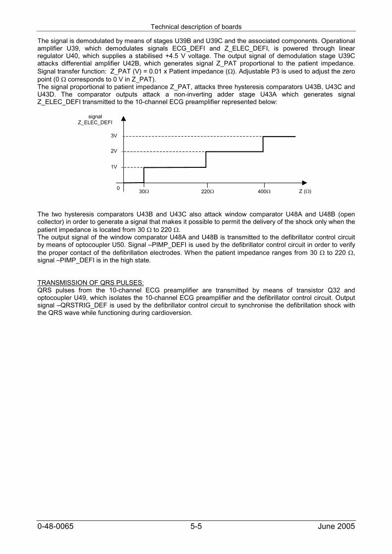
The signal is demodulated by means of stages U39B and U39C and the associated components. Operationalamplifier U39, which demodulates signals ECG_DEFI and Z_ELEC_DEFI, is powered through linearregulator U40, which supplies a stabilised +4.5 V voltage. The output signal of demodulation stage U39Cattacks differential amplifier U42B, which generates signal Z_PAT proportional to the patient impedance.Signal transfer function: Z_PAT (V) = 0.01 x Patient impedance (). Adjustable P3 is used to adjust the zeropoint (0 corresponds to 0 V in Z_PAT).The signal proportional to patient impedance Z_PAT, attacks three hysteresis comparators U43B, U43C andU43D. The comparator outputs attack a non-inverting adder stage U43A which generates signalZ_ELEC_DEFI transmitted to the 10-channel ECG preamplifier represented below:
0
signalZ_ELEC_DEFI
3V
Z ()22030 400
2V
1V
The two hysteresis comparators U43B and U43C also attack window comparator U48A and U48B (opencollector) in order to generate a signal that makes it possible to permit the delivery of the shock only when thepatient impedance is located from 30 to 220 .The output signal of the window comparator U48A and U48B is transmitted to the defibrillator control circuitby means of optocoupler U50. Signal –PIMP_DEFI is used by the defibrillator control circuit in order to verifythe proper contact of the defibrillation electrodes. When the patient impedance ranges from 30 to 220 ,signal –PIMP_DEFI is in the high state.
TRANSMISSION OF QRS PULSES:QRS pulses from the 10-channel ECG preamplifier are transmitted by means of transistor Q32 andoptocoupler U49, which isolates the 10-channel ECG preamplifier and the defibrillator control circuit. Outputsignal –QRSTRIG_DEF is used by the defibrillator control circuit to synchronise the defibrillation shock withthe QRS wave while functioning during cardioversion.
Technical description of boards
0-48-0065 5-6 June 2005
5.2.2.3. CIRCUIT INTERFACE D’ENTREE.
The input interface circuit performs the following functions: Interfacing of signals from defibrillation cartridges Interfacing of signals to defibrillation cartridges
OVERALL DESCRIPTION:The input interface circuit forms the signals from the defibrillation cartridges and controls the functioning ofthe indicators of the handheld paddle electrodes or the front of the device.If the handheld paddle electrode cartridge is being used, the input interface circuit generates analoguevoltage corresponding to the selected energy, signal AWSEL. The various signals –PCIS, DKY1 and DKY2relating to the pressing of Charge/Shock keys in order to set off the charging of the HV capacitor or thedefibrillation shock. Besides, the input interface circuit also supplies a signal when the graph starting key ispressed, namely signal RECB. The LEDs of the handheld paddles are switched on by signal DEFREADYfrom the defibrillator control circuit. If the adhesive electrode cartridge is being used, the signals for energyselection and triggering the charging of the HV capacitor come from the CPU board through the serial link.Signal –ANAB corresponds to pressing the Analyse key. Signal –ANAKL is used to control the lighting of theAnalyse LED. Signals –DMPR and DMTP are used to verify the presence of a defibrillation cartridge and forthe identification of the type of cartridge by the defibrillator control circuit.
INPUT SIGNAL INTERFACE:The energy selection by means of the knob on the handheld paddles is achieved by analogue voltage WREFmade up by divider R101 and R336 in parallel with the resistor put into the circuit by the energy selector in thepaddles themselves. Signal WREF is buffered by voltage follower U22A before it attacks analoguemultiplexer U14.The type of defibrillation cartridge put in place in DG5000 is identified by means of analogue voltage MOD1polarised by R280, R330 and a fixed resistor inside the various cartridges.The insertion of a defibrillation cartridge in the slot provided for that purpose is recognised by means of signalMOD0.The connection of a pair of adhesive electrodes at the connector provided on the adhesive electrodecartridge is detected by signal –ELECTR, which switches to the low status in that case.The triggering of a charge by means of the handheld paddles is achieved by signal –DCIS, whichcorresponds to the pressing of one of the keys Charge/Shock on the paddle electrodes. Signal –DCIS isgenerated by comparator U22B and the associated components from signal –PCIS from the handheld paddleelectrodes. Signal –DCIS switches to the low level when a Charge/Shock key is pressed.Signal DDIS1 corresponds to pressing a Charge/Shock key. The signal generated by comparator U22C isused by the defibrillation microcontroller during the defibrillation shock.Signal –DDIS2 from line DKY2, corresponds with the second signal used by defibrillation microcontroller U16during a defibrillation shock. Signal –DDIS2 generated by U22D switches to the low level when the twoCharge/Shock keys are pressed.The pressing of the graph starting key on a handheld paddle is detected by signal REC and throughcomparators U23A, U23B and logical gates U24A, U24B and U24C if the paddle electrode cartridge is used.Pressing the Analyse key on the front is recognised by means of signal –ANAKEY, which switches to the lowlevel when the key is pressed.
OUTPUT SIGNAL INTERFACE:The DEFI READY indication LEDs of the handheld paddles are switched on by means of lines READY and –READY. These signals are generated by transistor Q24 and open-collector driver U12F and also buffer U21Adriven by signal EPDU generated by the defibrillation microcontroller U16.If the adhesive electrode cartridge is being used, the LED of the Analyse key on the front is switched on byline ANALED. Line ANALED is driven by transistor Q23 and driver U12A, which is driven by signal ANKLgenerated by defibrillation microcontroller U16.
Technical description of boards
0-48-0065 5-7 June 2005
5.2.2.4. DEFIBRILLATOR CONTROL CIRCUIT
The defibrillator control circuit part carries out the following functions: Self test of the defibrillator part Transfer of information through a serial link to the CPU board Handling of information from defibrillation cartridges Control of the charging of the high-voltage capacitor Measurement of the energy stored in the high-voltage capacitor Triggering of the defibrillation shock if the Shock key is pressed Control of synchronised shock Determination of patient impedance during defibrillation shocks Control of the pulse biphasic waveform with patient impedance compensation Safety discharge of the high-voltage capacitor.
OVERALL DESCRIPTION:The defibrillator control circuit contains a microcontroller that carries out all the functions described above.When the device is switched on, the defibrillator control circuit runs a self test of the defibrillator part. Themicrocontroller of the defibrillator control circuit exchanges information with the CPU board through a seriallink that is decoupled from the CPU board by an optocoupler.During manual use (handheld paddle electrode cartridge), the microcontroller of the defibrillator control circuittakes account of the various signals from the input interface circuit in order to control the high-voltage circuit.Signal AWSEL is an analogue voltage that is determined by the energy selected by means of the knob on thehandheld paddle electrodes. The two signals –DMPR and DMTP indicate the presence of a defibrillationcartridge and the type of defibrillation cartridge respectively. If the graph triggering key on the handheldpaddle electrodes is pressed (signal RECB), the microcontroller transmits the information corresponding withthe pressing of the key to the CPU through the serial link.Signal –PCIS which indicates the pressing of one of the Charge/Shock keys of the handheld paddleelectrodes sets off the charting of the HV capacitor at the selected energy. Before triggering the charging ofthe HV capacitor, the microcontroller of the defibrillator control circuit checks if the Charge transistor isoperating correctly by means of signal CTFC. When the test is completed, the defibrillator control circuitgenerates the Charge transistor activation signal (signal EHVG). The safety discharge relay is also excited bymeans of signal WDRA. When the different operations are performed, the charging of the HV capacitor istriggered by the activation of the HV generator (signal LHVC). While the HV capacitor is being charged, themicrocontroller measures the energy stored in the HV capacitor through signal THVM. The microcontrolleralso generates two signals that block the IGBTs (signals PHASE1_B and PHASE2_B). If, during the chargingof the HV capacitor, the user selects a lower energy value, the microcontroller sets off a safety discharge ofthe HV capacitor by deactivating all the active outputs (deactivation of signals LHVC, WDRA and EHVG). Ifthe user selects a higher energy, the microcontroller sets off a compensation charge by means of signalLHVC till the new selected energy value is reached. When the stored energy is equal to the selected energy,the microcontroller stops the HV generator by means of signal LHVC.The defibrillator is now in the hold phase, during which the two LEDs of the handheld paddle electrodes areswitched on by means of signals EPDU and READY. During this phase, the stored energy is measured bysignal CHVM. During the hold phase, simultaneously pressing the two keys Charge/Shock triggers thedefibrillation shock through two independent channels. The first channel for triggering the shock is directlymade up of the signal resulting from the serial arrangement of the two keys Charge/Shock in the handheldpaddle electrodes (signal DKY2). The second channel for triggering the defibrillation shock is made up of themicrocontroller of the defibrillator control circuit (signal UPRA) lasting 100 ms. The two signals above activatethe patient relay of the high-voltage unit. After a 25-ms time, the first defibrillation pulse is generated by theIGBT control circuit. During the first pulse, the microcontroller measures the defibrillation current by means ofsignal IPAT in order to determine the patient impedance. Once that has been determined, the microcontrolleradapts the cyclic ratio of the defibrillation wave to the calculated impedance.During the shock, the IGBTs are driven by the IGBT control circuit (signals PHASE1_C and PHASE2_C) togenerate the pulse biphasic wave with patient impedance compensation. After a duration of 100ms, signalUPRA deactivates the patient relays and disables the IGBT control circuit. The microcontroller deactivates allthe outputs and the energy remaining in the HV capacitor is dissipated in the safety discharge circuit. Duringthe defibrillation shock, the microcontroller calculates the energy delivered and transmits the value and thepeak current and the patient impedance to the CPU board.In the case of synchronised defibrillation, the microcontroller generates signal UPRA only in the presence of asynchronisation pulse in relation to the QRS wave, signal –QRSTRIG.If the adhesive electrode cartridge is being used, the energy is selected (in manual mode) by means of thefunction keys on the front of the device and the selected energy value is transmitted by the CPU board to thedefibrillator microcontroller by means of the serial link.
Technical description of boards
0-48-0065 5-8 June 2005
In the SAD operating mode, the microcontroller of the defibrillator control circuit checks if the Analyse key ofthe front has been pressed (signal -ANAB) and transmits the corresponding information through the serial linkto the CPU board. If the master microprocessor of the CPU board recognises VF/VT, the CPU board sends arequest for pre-charging and the selected energy through the serial link. That pre-charge control starts off theprocess of charging the HV capacitor as described above. When the energy stored is equal to the selectedenergy, the microcontroller stops the HV generator and the defibrillator circuit is located in the phase whenthe pre-charge is completed, where the defibrillation shock is as yet not authorised. During that phase, themicrocontroller measures the energy stored in the HV capacitor by means of signal CHVM. If, during theprevious phase, an analysis of the ECG signal of the CPU board confirms VF/VT, the CPU board sends anew request for charging to the defibrillator circuit. The defibrillator control circuit once again activates the HVgenerator (signal LHVC) till the new selected energy is reached. When the energy stored in the HV capacitoris equal to the selected energy, the microcontroller stops the HV generator and authorises the defibrillationshock (signal EPDU). In that case, the Defi Ready LEDs of the Shock key on the front go on and thedefibrillation shock is triggered by pressing by the Shock button.
SELF TEST OF THE DEFIBRILLATOR PART:The defibrillator control circuit part is powered by the +5V voltage that is generated independently by linearregulator U13. When the DG 5000 device is started up, circuits U12D and U7D generate a reset of themicrocontroller of the defibrillator control circuit. The +5V power voltage is monitored by the BOR functionintegrated to microcontroller U16, which resets U16 if it fails (when the voltage drops below +4.5 V). Themaster microprocessor of the CPU board can also generate a reset of U16 through signal DE_µC_RST thatdrives optocoupler U19. The voltage reference of the ADC internal to U16 is made up by U20.
When the DG 5000 device is switched on, microcontroller U16 of the defibrillator control circuit runs a selftest of the defibrillator part. During the self test, microcontroller U16 does the following: Configuration of input/output ports Check of the proper operating of the serial link with the CPU board Check of program integrity Check of the proper operating of the fault detection circuit Check of the proper operating of the ADC Check of the proper operating of the voltage reference of the fault detection circuit (U8) and analogue
multiplexer U14. Check of signal –DDIS2. Check of the status of the Charge transistor (Q1) Check of the charging voltage of the HV capacitor
During the self test, all the output ports of the microcontroller are deactivated. The operating of fault latchU10A is tested by signal –SFDU, which must trigger latch U10A by means of gate U7B. In order to check theproper working of the latch, microcontroller U16 reads signal FDUO by means of multiplexer U15. During thetest, signal FDUO must be high. When the test result confirms the proper operating of the safety latch,microcontroller U16 resets U10A by means of signal –RFDU.The ADC internal to microcontroller U16 is tested by reading the +5 V and GND voltage via analoguemultiplexer U14. Voltage reference U8 (+2.5 V) is also verified by analogue multiplexer U14. That voltagereference is used by the fault detection circuit comparators.During the self test, the microcontroller also checks the status of buttons Charge/Shock by means of signal –DDIS2. Signal –DDIS2 comes from the serial arrangement of the two keys Charge/Shock and is formed byU22D and the associated components. During the test (when the two keys are not pressed), signal –DDIS2must be on the high level.The status of Charge transistor Q1 is verified by means of signal CTFC. Signal CTFC corresponds to thevoltage present on the drain of Q1, divided by R140 and R141. During the self test, signal CTFC must beclose to 0 V.The charging voltage of the HV capacitor is verified by means of signal CHVM, also via analogue multiplexerU14. During the self test, the charging voltage of the HV capacitor must be close to 0 V (HV capacitordischarged).In a fault is detected during the self test, microcontroller U16 sends an error message to the CPU board bymeans of the serial link. In that case, U16 deactivates all the outputs so as to block the operating of the high-voltage part of the defibrillator. When the defibrillator circuit self test is completed without detecting a fault,the defibrillator enters the standby phase.
Technical description of boards
0-48-0065 5-9 June 2005
EXCHANGE OF INFORMATION BY THE SERIAL LINK WITH THE CPU BOARD:The transfer of information between the CPU board and the defibrillator part is achieved by means of a seriallink. In the defibrillator circuit, the serial link is directly managed by microcontroller U16, signals RxD and TxD.The transmission of the information from the serial link to the CPU board is achieved by means ofoptocouplers U17 and U18. The dialogue through the serial link takes place by sending a frame every 100ms.The serial link transmits the following information: Information for testing proper communication between the CPU board and the defibrillator Information about the malfunctioning of the defibrillator part Information about the standby phase of the defibrillator part Information about the charging phase of the HV capacitor Information about the pre-charge completed status Information about the hold phase of the HV capacitor Information about the application of the shock defibrillation Information about the safety discharge phase Real time information about the energy stored during the charging or hold phase of the HV capacitor Information about operating in direct or synchronous mode Information about the energy delivered during the application of the defibrillation shock Information about the peak current during the application of the defibrillation shock Information about the identification of the defibrillation cartridge put in place and the connection of a pair of
adhesive electrodes Information about the pressing of a graph triggering key on the handheld paddle electrodes Information about the pressing of the Analyse key on the front of the device Information leading to a battery test Information about the energy selected if an adhesive electrode cartridge is in use Information about the triggering of the pre-charge to the selected energy value Information about the triggering of the charge to the selected energy value Information about the safety discharge of the HV capacitor
CONTROL OF THE HIGH-VOLTAGE CAPACITOR CHARGE:
STANDBY PHASE:During the standby phase, microcontroller U16 dialogues with the master microprocessor of the CPU boardby means of the serial link. The high-voltage circuit of the defibrillator part is disabled. The controlling of thecharging of the HV capacitor is started either by signal –DCIS, if the handheld paddle electrode cartridge isbeing used, or by the master microprocessor of the CPU board via the serial link if the adhesive electrodecartridge is being used. In semiautomatic mode, two pieces of information are used to trigger the charging ofthe HV capacitor - the pre-charge information and the charge information. In both cases, the procedure of ccharging the HV capacitor is identical. The difference lies in the status of the defibrillator after charging iscomplete. If the HV capacitor is charged by the pre-charge command, the defibrillator goes into the pre-charge completed state when charging is complete. During the pre-charge completed phase, the defibrillatorstands by for a new charging request and does not allow the delivery of defibrillation shocks. If the HVcapacitor is charged by the charge command, the defibrillator enters the hold phase when charging iscomplete. During the hold phase, the defibrillator authorises the defibrillation shock. When the charging orpre-charging is triggered, the master microprocessor also sends a signal corresponding to the selectedenergy.
CHARGE PHASE:The charge phase is either triggered by signal –DCIS or, while using the adhesive electrode cartridge, by thecharge signal from the master microprocessor to the serial link. When charging is triggered, microcontrollerU16 checks the Charge transistor (Q1) through signal CTFC. After verifying signal CTFC, microcontroller U16activates Charge transistor Q1 and Q2 through signal EHVG and open-collector driver U12B. The activationof Q1 generates the high-current power voltage of the HV generator +UCHARGE from the DC voltagesupplied by the Power Board. That +UCHARGE voltage is protected by fuse F1. The activation of transistorQ2 generates the power supply voltage of chopping regulator U1.Microcontroller U16 also activates signal WDRA, which excites the safety discharge relay RL1 by means ofbuffer U21E and transistor Q11A. After a 50-ms time, microcontroller U16 activates the HV generator bymeans of signal LHVC and buffer U21B. When all the conditions are met, the HV capacitor starts charging.The maximum time of the charge initiated by signal –DCIS or a charge command via the serial link is limitedto 30 s (in the event of a problem), after which U16 triggers the safety discharge of the HV capacitor bydeactivating all the active outputs.
Technical description of boards
0-48-0065 5-10 June 2005
In order to actively block the IGBTs of the HV switching circuit, microcontroller U16 also generates twosignals PHASE1_B and PHASE2_B with a period of 16 ms and a duration of 200 µs. The two signalsPHASE1_B and PHASE2_B generate blocking pulses in the cores that drive the gates of the IGBTs throughdrivers U5B and U6B and transistors Q19 and Q21. Microcontroller U16 generates these IGBT blockingpulses during the charge, pre-charge completed and hold phases.During the charge phase of the HV capacitor, microcontroller U16 measures the charging voltage of the HVcapacitor through signal THVM via multiplexer U14. The energy stored in the HV capacitor is calculated byU16. When the value is equal to the selected energy, U16 deactivates the LHVC signal, which stops thecharging of the HV capacitor.
HOLD PHASE:When the defibrillator enters the hold phase, microcontroller U16 determines the energy stored in the HVcapacitor by means of signal CHVM and checks that it is located within the permitted tolerances. If that is notso, U16 triggers a safety discharge of the HV capacitor. During the hold phase, microcontroller U16 activatessignal EPDU, which makes Q11B conduct through open-collector driver U12C. In these conditions, thedefibrillation shock may be delivered to the patient. The hold phase does not last longer than 20 s, after whichmicrocontroller U16 triggers a safety discharge.
PRE-CHARGE PHASE:In the semiautomatic mode using the adhesive electrode cartridge, the master microprocessor of the CPUboard initiates a pre-charge of the capacitor during the analysis of the ECG signal. The pre-charge commandand the selection of the corresponding energy value is transmitted by the serial link to the defibrillator. Thepre-charge process is identical to the charge process, and the maximum duration of the pre-charge phase is20 s. When the energy stored in the HV capacitor is equal to the selected energy, microcontroller U16 entersthe pre-charge completed phase.
PRE-CHARGE COMPLETED PHASE:After the pre-charge phase, the defibrillator enters the pre-charge completed phase. During this pre-chargecompleted phase, microcontroller U16 calculates the energy stored in the HV capacitor by means of signalCHVM and stands by for a new charging request. During the pre-charge completed phase, signal EPDUremains low and the defibrillation charge is not validated. The maximum duration of the pre-chargecompleted phase is set to 15 s. After that time, microcontroller U16 triggers a safety discharge of the HVcapacitor by deactivating all the outputs.If, during the pre-charge completed phase, U16 receives a new signal requesting a charge to the selectedenergy, the microcontroller goes back to the charge phase by activating signal LHVC.
MEASUREMENT OF THE ENERGY STORED IN THE HIGH-VOLTAGE CAPACITOR:The energy stored in the HV capacitor is measures by means of two independent signals, THVM and CHVM.During the HV capacitor charge sequences, the stored energy is measured by signal THVM. Signal THVMcomes from the primary winding of the HV converter and is formed by Q3, U2A and U2C. Signal THVM isdirectly proportional to the charge voltage of the HV capacitor.During the pre-charge completed and hold phases, the stored energy is measured by signal CHVM. SignalCHVM is directly taken at the terminals of the HV capacitor, by means of resistive dividers with a high ohmicvalue (R251, R252 and R259 and R253, R254 and R206) referenced in relation to the ground. The twosymmetrical voltages obtained are amplified by differential amplifier U4C.
TRIGGERING OF THE DEFIBRILLATION SHOCK:If, during the hold phase, the two keys Charge/Shock of the handheld paddle electrodes or the Shock key onthe front is pressed, the defibrillator triggers the defibrillation shock. When the two keys Charge/Shock of thehandheld paddle electrodes or the Shock key on the front of the device are pressed in, line DKY2 isconnected to the ground. When line DKY2 is low, patient relays RL2 and RL3 are excited by two independentcontrol channels.The first channel for activating the patient relay RL2, RL3 is made up of transistor Q12B and buffer U21Ddriven by signal UPRA generated by microcontroller U16. When one of the Shock keys is pressed,comparator U22D makes signal –DDIS2 switch to low. Signal –DDIS2 is taken into account by microcontrollerU16. When signal–DDIS2 is active for more than 150ms, U16 generates a high level on signal UPRA for100ms.The second channel for activating the patient relay is made up of transistor Q12A that is activated directly byline DKY2 and transistors Q9 and Q10. In order to excite the patient relay, the two triggering channels mustbe active.
Technical description of boards
0-48-0065 5-11 June 2005
Direct or synchronised shock operation is defined by the master microprocessor through a piece ofinformation in the serial link. In the event of synchronised defibrillation, the shock is only delivered in thepresence of a syncing pulse on the QRS wave, signal -QRSTRIG. In this operating mode, the shock is alsogiven by the two distinct control channels. The first of them is made up by microcontroller U16, which in thiscase generates signal UPRA, only when the two keys Charge/Shock are pressed and there is asynchronisation pulse on signal –QRSTRIG. The second channel is made up by gate U7C driven by U16according to the operating mode - direct or synchronous. In the synchronous shock operating mode, thesignal SYNC is high. In this case, the syncing pulses from U21C and the differentiating network C146, R347triggers high syncing pulses at the output of U7C. These pulses enable the activation of transistor Q10through open-collector driver U12E. If, in these conditions, the Shock key or keys are simultaneously pressedand a synchronising pulse is present, the patient relays are activated by transistors Q9, Q10, Q12A, Q12Band the associated components. The activation duration of patient relays RL2 and RL3 is defined by signalUPRA, which lasts 100 ms.During the 100 ms of activation of patient relays RL2 and RL3, the patient is connected to the high-voltagecircuit of the defibrillator.
DRIVING THE BIPHASIC WAVE WITH PATIENT IMPEDANCE COMPENSATION:The first IGBT control pulse (first defibrillation shock pulse) is generated 25 ms after the rising edge of signalUPRA. That first pulse of signal PHASE1_C makes the first-phase IGBTs conduct, namely Q13 and Q14.While the IGBTs are conducting the microcontroller measures the patient peak current.The patient peak current is measured by means of signal IPAT taken from the patient discharge circuit bycurrent transformer TR2. The signal from the secondary winding of current transformer TR2 is filtered andbuffered by U2B and the associated components before it is amplified by U2D to supply signal IPAT.From the charging voltage of the HV capacitor (signal CHVM) and the patient current value (signal IPAT),microcontroller U16 determines the value of the patient impedance.After calculating the patient impedance value, microcontroller U16 direct adapts the cyclic ratio of the IGBTcontrol signals to the patient impedance. Signals PHASE1_C and PHASE2_C lead to the driving of the IGBTsof the first phase (Q13, Q14) and the second phase (Q15, Q16 and Q17, Q18) respectively. Durations Tonand Toff (determined by microcontroller U16) of signals PHASE1_C and PHASE2_C make the IGBTs of thehigh-voltage switching circuit conduct or not in order to generate the pulse biphasic wave with patientimpedance.After 100 ms, signal UPRA deactivates patient relay RL2, RL3. Microcontroller U16 deactivates all its outputs,signals EPDU, WDRA and EHVG are switched to low, leading to a safety discharge of the energy remainingin the HV capacitor. During the defibrillation shock, microcontroller U16 also calculates the energy deliveredto the patient and transmits the corresponding information and the value of the peak current and the patientimpedance to the master microprocessor of the CPU board.
SHOCK OUTSIDE THE NOMINAL IMPEDANCE RANGE:When the Shock key or keys is/are pressed, microcontroller U16 first checks the status of signal -PIMP whichcorresponds to the patient impedance range in which the defibrillation shock is permitted. When signal -PIMPis high, the patient impedance ranges from 30 to 220 and the defibrillation shock is allowed. When signal-PIMP is low, microcontroller U16 does not permit the defibrillation shock and directly leads to a safetydischarge of the HV capacitor. Signal -PIMP is taken from the ECG preamplifier part and transmitted byoptocoupler U50.
HV CAPACITOR SAFETY DISCHARGE:The HV capacitor safety discharge may be initiated either directly by microcontroller U16 when it enters thesafety discharge phase or by a safety discharge command from the master microprocessor of the CPUboard, or by the fault detection circuit by means of fault latch U10A. In any event, the safety discharge of theHV capacitor is triggered by a return to the low level of signal WDRA.
Technical description of boards
0-48-0065 5-12 June 2005
5.2.2.5. HIGH-VOLTAGE CIRCUIT
The high-voltage circuit part carries out the following functions: Patient insulation from the high-voltage circuit Charging the HV capacitor to the defined energy value Measuring the HV capacitor charging voltage Blocking the high-voltage switching circuit Generating the pulse biphasic wave with patient impedance compensation Measuring the peak value of the defibrillation current Safety discharge of the HV capacitor
OVERALL DESCRIPTION:The high-voltage circuit insulates the patient from the high-voltage unit of the defibrillator by means of twopatient relays. The defibrillator charging circuit is directly powered by the DC voltage from the power circuit -Power Board. The high-voltage unit is activated by the Charge transistor (signal EHVG). The HV capacitor ischarged by the HV generator (signal LHVC). When the HV capacitor is charged, the safety discharge relay isalso activated (signal WDRA). During the charging of the HV capacitor, the HV generator supplies a signal tomeasure the charge voltage by the primary winding of the HV converter (signal THVM). The signal is used bythe defibrillator control circuit to determine the energy stored in the HV capacitor. When the energy stored inthe HV capacitor is equal to the selected energy, the HV generator is deactivated, which stops the charge.When the defibrillator is in the hold phase, the charge voltage is measured by two symmetrical high-voltagedividers at the terminals of the HV capacitor (signal CHVM). The two HV dividers are referenced in relation tothe ground. During the charge and hold phases, the high-voltage circuit actively blocks the IGBTs of the HVswitching circuit by means of the pulse transformers associated with the IGBTs. The active blocking of theIGBTs is controlled by the microcontroller (signals PHASE1_B and PHASE2_B). During the entire duration ofthe hold phase, the activation of the patient relay control stage is authorised (signal EPDU). When the twokeys Charge/Shock are pressed on the handheld paddle electrodes are pressed simultaneously or the Shockkey on the front is pressed, the defibrillator control circuit activates the patient relay for 100ms (signals UPRAand DKY2). The IGBT control circuit controls the high-voltage switching stage with IGBTs in order to generatethe pulse biphasic wave with patient impedance compensation (signals PHASE1_C and PHASE2_C). In theevent of synchronised defibrillation, shock synchronisation is also driven by two distinct channels. The first ofthese is made up of signal –SYNC and it directly activates the patient relay if a synchronisation pulse ispresent on the QRS wave while the two Charge/Shock keys are pressed. The second channel is made up ofthe microcontroller, which generates the UPRA signal in the synchronised defibrillation mode only if the thereis a QRS synchronisation pulse and the two keys Charge/Shock are pressed. The syncing signal –QRSTRIG_DEF is taken from the floating part of the 10-channel ECG preamplifier and transmitted to thedefibrillator control circuit by means of an optocoupler in the defibrillator ECG preamplifier part.During the first current pulse of the defibrillation wave, the high-voltage circuit measures the patient currentvalue by means of current transformer TR2, which generates signal IPAT after it is formed. This piece ofinformation enables the defibrillator control circuit to determine the patient resistance in order to drive theIGBT control circuit.The high-voltage circuit also enables the safety discharge of the HV capacitor through a power resistanceand the safety discharge relay. The safety discharge of the HV capacitor is driven by the defibrillator controlcircuit (signal WDRA). The safety discharge may be initiated either directly by the microcontroller of thedefibrillator circuit or by information transmitted by the serial link from the CPU board.
PATIENT INSULATION FROM THE HIGH-VOLTAGE CIRCUIT:The patient is insulated from the high-voltage circuit by means of the open contacts of patient relay RL2 andRL3 of the defibrillator part. In the idle position, the HV contacts of the defibrillation electrodes are connectedto the optional pacemaker if it is present. During the 100-ms activation time during the defibrillation shock, thepacemaker is disconnected from the defibrillator through working contacts of the patient relay.An ECG signal taken by the defibrillation electrodes is sent by means of optocoupler U37 in the floating partof the 10-channel ECG preamplifier. The floating part of the defibrillation ECG preamp is further insulated byoptocouplers U35, U36, U38 and transformer TR3.
Technical description of boards
0-48-0065 5-13 June 2005
CHARGING THE HV CAPACITOR TO THE DEFINED ENERGY VALUE:If the handheld paddle electrode cartridge is being used, the energy is selected by means of signal WREF. Ifthe adhesive electrode cartridge is being used, the energy is selected by the master microprocessor, whichtransmits the corresponding information to microcontroller U16 via the serial link. After receiving a chargerequest, either through signal –DCIS or through charge information in the serial link, the microcontrollerchecks the CTFC signal to check that there is no voltage at the drain of the Charge transistor Q1. When thatcondition is met, signal -EHVG switches to low, which makes Q1 and Q2 conduct. When Charge transistorQ1 conducts, that makes voltage +UCHARGE appear. When Q2 conducts, chopping regulator U1 is suppliedwith +12 V. Microcontroller U16 also controls the activation of the safety discharge relay, RL1, by signalWDRA and transistor Q11A. In those conditions, the contacts of the safety discharge relay RL1 are open,making it possible to charge the HV capacitor. The charging of the HV capacitor is started by means of signalLHVC, which switches to high. When signal LHVC is high, transistor Q5 unlocks the HV generator builtaround U1, Q6, Q7 and associated components, leading to the charging of the HV capacitor 40 µF / 3.1 kVby means of the secondary winding of transformer HT, TR1.
MEASUREMENT OF THE CHARGING VOLTAGE OF THE HV CAPACITOR:The charging voltage of the HV capacitor is measured by means of two different circuits.The first circuit that measures the charging voltage of the HV capacitor is made up of resistors R251, R252and R259 and also R253, R254 and R260, which directly take the charging voltage at the terminals of the HVcapacitor. Signals HV_M+ and HV_M- generated by the resistive divider attack the differential amplifier U4C,which supplies signal CHVM used as the measuring signal by microcontroller U16. Signal CHVM indicatesthe charging voltage of the HV capacitor divided by 850.The second circuit that measures the charging voltage of the HV capacitor only generates a signal during thecharging phases of the HV capacitor. The measurement signal is taken by means of the primary winding ofHV transformer TR1, which reflects the charging voltage of the HV capacitor when transistor Q7 is blocked.The signal from the primary winding of TR1 is taken by transistor Q3 and the associated components. StagesU2A and U2C make up the forming circuits of the signal supplied by Q3. The output signal from U2C, THVM,also indicates the charging voltage of the HV capacitor divided by 850. Signal THVM is used bymicrocontroller U16 to measure the charging voltage of the HV capacitor in order to stop charging the HVgenerator. The charge stopping is adjusted by means of adjustable P1.
HV SWITCHING CIRCUIT BLOCKING:During the charge, pre-charge completed and hold phases, the microcontroller generates two signals,PHASE1_B and PHASE2_B, which actively block IGBTs Q13, Q14, Q15, Q16, Q17 and Q18 of the HVswitching circuit. The IGBTs are blocked by signals PHASE1_B and PHASE2_B, which control the primarycurrent of the IGBT control cores L1, L2, L3, L4, L5 and L6 through drivers U5B, U6B and transistors Q19and Q21. While driving the cores of transistors Q19 and Q21, the secondary windings of the controls coresgenerate a negative gate voltage in order to effectively block the IGBTs of the two phases.
GENERATION OF THE BIPHASIC WAVE WITH PATIENT IMPEDANCE COMPENSATION:The biphasic wave with patient impedance is generated by means of signals PHASE1_C and PHASE2_C.These two signals drive the primary current of the control cores of the IGBTs by means of drivers U5A, U6Aand transistors Q20 and Q22. The primary current of cores is limited by resistors R237, R420 and R238,R239. While the cores are driven by transistors Q20 and Q22, the secondary windings generate positive gatevoltage (on the rising edges of signals PHASE1_C and PHASE2_C), which makes the IGBTs of phase 1 orphase 2 conduct, and negative gate voltage (on the falling edges of signals PHASE1_C and PHASE2_C),which blocks the IGBTs of phase 1 or phase 2.The biphasic wave defibrillation shock with patient impedance compensation is achieved by the successiveconducting and blocking phases of IGBTs Q13 - Q18, which form an H bridge enabling biphasic discharge.The first phase of the biphasic wave is provided by conduction by Q13 and Q14 and the second byconduction by Q15, Q16 and Q17, Q18. The high-voltage switching circuit with IGBTs is connected to thepatient by means of the patient relay made up of RL2 and RL3. The patient relay control is made up of signalUPRA and line DKY2. The first signal UPRA, which drives transistor Q12B, is generated by microcontrollerU27 of the defibrillator control circuit. Signal UPRA has a duration of 100 ms. The second control signalcomes directly from the serial application of the two Charge/Shock keys of the handheld paddle electrodes orthe Shock key on the front of the device. In the direct shock operating mode (Q10 saturated), line DKY2activates transistor Q9, which saturates Q12A by means of network D6, C91 and R123. Transistor Q10controls the hardware of the patient relay in the event of a synchronised shock. When the two transistorsQ12A, Q12B conduct and the defibrillator is in the hold phase, the patient relay is activated for a duration of
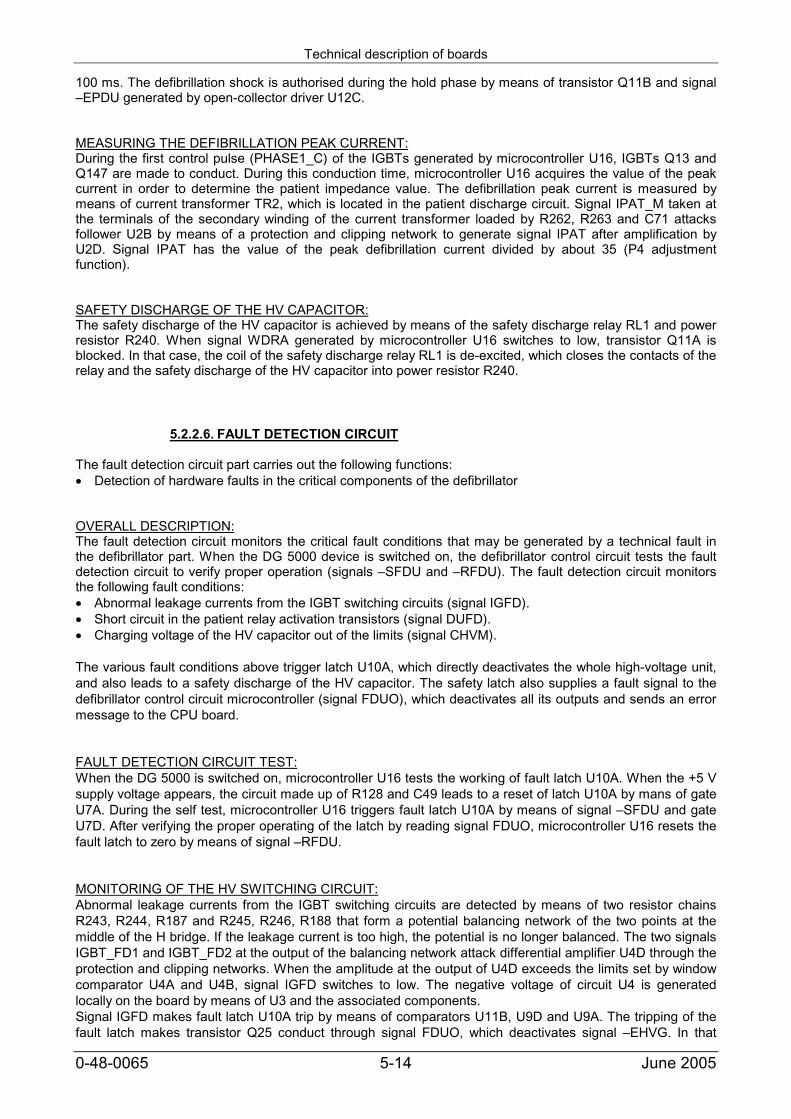
Technical description of boards
0-48-0065 5-14 June 2005
100 ms. The defibrillation shock is authorised during the hold phase by means of transistor Q11B and signal–EPDU generated by open-collector driver U12C.
MEASURING THE DEFIBRILLATION PEAK CURRENT:During the first control pulse (PHASE1_C) of the IGBTs generated by microcontroller U16, IGBTs Q13 andQ147 are made to conduct. During this conduction time, microcontroller U16 acquires the value of the peakcurrent in order to determine the patient impedance value. The defibrillation peak current is measured bymeans of current transformer TR2, which is located in the patient discharge circuit. Signal IPAT_M taken atthe terminals of the secondary winding of the current transformer loaded by R262, R263 and C71 attacksfollower U2B by means of a protection and clipping network to generate signal IPAT after amplification byU2D. Signal IPAT has the value of the peak defibrillation current divided by about 35 (P4 adjustmentfunction).
SAFETY DISCHARGE OF THE HV CAPACITOR:The safety discharge of the HV capacitor is achieved by means of the safety discharge relay RL1 and powerresistor R240. When signal WDRA generated by microcontroller U16 switches to low, transistor Q11A isblocked. In that case, the coil of the safety discharge relay RL1 is de-excited, which closes the contacts of therelay and the safety discharge of the HV capacitor into power resistor R240.
5.2.2.6. FAULT DETECTION CIRCUIT
The fault detection circuit part carries out the following functions: Detection of hardware faults in the critical components of the defibrillator
OVERALL DESCRIPTION:The fault detection circuit monitors the critical fault conditions that may be generated by a technical fault inthe defibrillator part. When the DG 5000 device is switched on, the defibrillator control circuit tests the faultdetection circuit to verify proper operation (signals –SFDU and –RFDU). The fault detection circuit monitorsthe following fault conditions: Abnormal leakage currents from the IGBT switching circuits (signal IGFD). Short circuit in the patient relay activation transistors (signal DUFD). Charging voltage of the HV capacitor out of the limits (signal CHVM).
The various fault conditions above trigger latch U10A, which directly deactivates the whole high-voltage unit,and also leads to a safety discharge of the HV capacitor. The safety latch also supplies a fault signal to thedefibrillator control circuit microcontroller (signal FDUO), which deactivates all its outputs and sends an errormessage to the CPU board.
FAULT DETECTION CIRCUIT TEST:When the DG 5000 is switched on, microcontroller U16 tests the working of fault latch U10A. When the +5 Vsupply voltage appears, the circuit made up of R128 and C49 leads to a reset of latch U10A by mans of gateU7A. During the self test, microcontroller U16 triggers fault latch U10A by means of signal –SFDU and gateU7D. After verifying the proper operating of the latch by reading signal FDUO, microcontroller U16 resets thefault latch to zero by means of signal –RFDU.
MONITORING OF THE HV SWITCHING CIRCUIT:Abnormal leakage currents from the IGBT switching circuits are detected by means of two resistor chainsR243, R244, R187 and R245, R246, R188 that form a potential balancing network of the two points at themiddle of the H bridge. If the leakage current is too high, the potential is no longer balanced. The two signalsIGBT_FD1 and IGBT_FD2 at the output of the balancing network attack differential amplifier U4D through theprotection and clipping networks. When the amplitude at the output of U4D exceeds the limits set by windowcomparator U4A and U4B, signal IGFD switches to low. The negative voltage of circuit U4 is generatedlocally on the board by means of U3 and the associated components.Signal IGFD makes fault latch U10A trip by means of comparators U11B, U9D and U9A. The tripping of thefault latch makes transistor Q25 conduct through signal FDUO, which deactivates signal –EHVG. In that
Technical description of boards
0-48-0065 5-15 June 2005
case, the power supply voltage +UCHARGE disappears, which stops the HV generator if it is charging andthe leads to the safety discharge of the HV capacitor. The tripping of fault latch U10A also generates faultinformation recognised by microcontroller U16 by means of signal FDUOS. Microcontroller U16 deactivatesall its outputs and supplies an error message transmitted to the CPU board by means of the serial link.
MONITORING OF THE PATIENT RELAY ACTIVATION TRANSISTORS:The detection of faults in transistors Q12A and Q12B that activate the patient relay is achieved by means ofsignal DUFD. If one of the transistors is shorted, the idle potential of signal DUFD polarised by resistors R97and R98 is modified. The variation is detected by means of the window comparator made up of U11C andU11D. After a duration of about 2.5 s, fault latch U10A is tripped by means of U11A, U9C and U9A. Asdescribed above, the tripping of the fault latch makes transistor Q25 conduct by means of signal FDUO andtherefore the safety discharge of the HV capacitor (see previous paragraph, Monitoring of the HV switchingcircuit).
MONITORING OF THE HV CAPACITOR CHARGE VOLTAGE:Overvoltage in the event of a fault in the charge stopping circuit is detected by comparator U9B, whichmonitors the amplitude of signal CHVM. When the charging voltage of the HV capacitor reachesapproximately 3.3 kV, signal CHVM divided by R269 and R273 makes comparator U9B trip, which activatesfault latch U10A by means of U9A. The safety discharge of the HV capacitor and the stopping of the HVgenerator is achieved as described earlier (see previous paragraph, Monitoring of the HV switching circuit).
Technical description of boards
0-48-0065 5-16 June 2005
5.2.3. CHRONOGRAMS
5.2.3.1. HV CAPACITOR CHARGE.
t0
t0
t0
t0
t0
t0
t0
t0
signal-DCIS
signalPHASE2_B
signalEHVG
+ UCHARGEDrain Charge
Transistor
signalWDRA
LHVC
VDSSwitchingtransistor
signalTHVM
+ UBATT
Internal dischargerelay activation
50 ms
+ UBATT
signalCHVM
70 V
Voltage referencefor 180 J
VREF = 3,65 V
pour U HT = 3101 V ( 180 J )CHVM = 3101 / 850 = 3,65 V
+ 3,65 V
End of charge
CHARGE REQUEST
t0 Tmin = 100 ms
t0
signalPHASE1_B
Technical description of boards
0-48-0065 5-17 June 2005
5.2.3.2. HV CAPACITOR PRE-CHARGE AND CHARGE
Semiautomatic mode operation
t0
t0
t0
signalWDRA
signalLHVC
signalEPDU
t0
+ UDISCHENDrain Discharge
Enable Transistor
50 ms
50 ms Tmax = 20 s
+ UBATT
t0
signalEHVG
Defi state
Beginning of charge
PRE-CHARGEREADY STATE
WAITSTATE
READYSTATE
CHARGESTATE
INTERNALDISCHARGE
STATE
CHARGESTATE
Tmax = 30 s
Tmax = 20 s
Tmax = 15 s
t0
signalPHASE1_B
t0
signalPHASE2_B
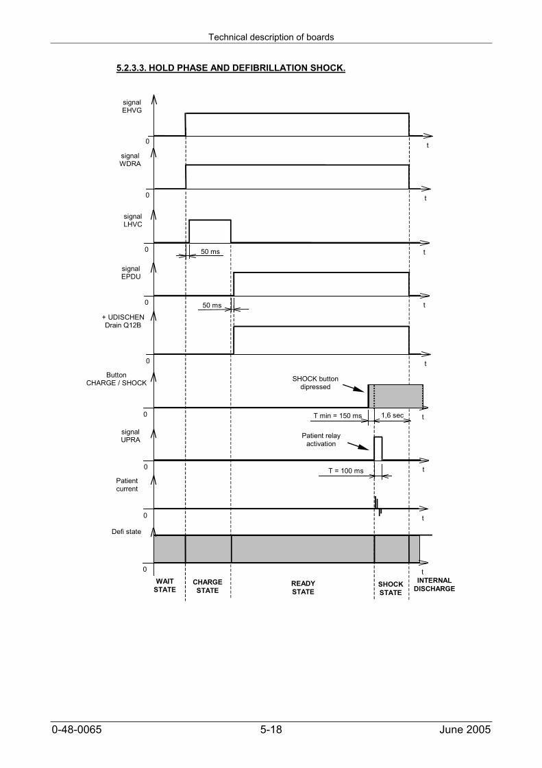
Technical description of boards
0-48-0065 5-18 June 2005
5.2.3.3. HOLD PHASE AND DEFIBRILLATION SHOCK.
t0
t0
t0
signalWDRA
signalLHVC
signalEPDU
t0
+ UDISCHENDrain Q12B
50 ms
50 ms
t0
signalEHVG
t0
ButtonCHARGE / SHOCK SHOCK button
dipressed
INTERNALDISCHARGE
T min = 150 ms 1,6 sec
Defi state
WAITSTATE
READYSTATE
CHARGESTATE
SHOCKSTATE
t0
t0
t0
signalUPRA
Patientcurrent
Patient relayactivation
T = 100 ms
Technical description of boards
0-48-0065 5-19 June 2005
5.2.4. DESCRIPTION OF SIGNALS
The names of signals refer to chart DG 5000 Defibrillator circuit.
5.2.4.1. ECG PREAMPLIFIER
ECG preamplifier input signals:
+VFM: Positive floating power supply voltage.+5 V supply voltage generated in the floating part of the 10-channel ECG preamplifier circuit. This power supply voltage ranges from +4.8 V to +5.2 V.
-VFM: Negative floating power supply voltage.-6 V supply voltage generated in the floating part of the 10-channel ECG preamplifier. This power supply voltage ranges from –5.5 V to –6.5 V.
FGND: Floating reference potentialReference potential (floating ground) of the floating part of the 10-channel ECG preamplifier. Floating reference potential 0 V.
STERNUM: ECG signal from the defibrillation electrode connectorSignal STERNUM is used to acquire the patient ECG signal by means of the defibrillation electrodesconnected to the defibrillation electrode connector.During the defibrillation shock, signal STERNUM is connected to the high-voltage circuit of the defibrillator bythe patient relay. Signal for acquiring the patient ECG through the defibrillation electrodes.
APEX: ECG signal from the defibrillation electrode connector.Signal APEX is used to acquire the patient's ECG signal through the defibrillation electrodes connected to thedefibrillation electrode connector.During the defibrillation shock, signal APEX is connected to the high-voltage circuit of the defibrillator by thepatient relay. signal for acquiring the ECG patient through the defibrillation electrodes.
INH_PACE: Pacemaker Inhibition.Logical signal generated by the microcontroller in the floating part of the 10-channel ECG preamplifier circuitfor activating an analogue switch in the amplification chain of the ECG signal if pacemaker pulses arerecognised. Signal INH_PACE is referenced in relation to FGND. If pacing pulses are detected, signalINH_PACE becomes active for the duration of the pacing pulse. Input signal INH_PACE ranges from 0V to +5V. The signal is active when low (active at 0V).
10 Hz: 10 Hz Test Signal.Logical signal generated by the microcontroller in the floating part of the circuit 10-channel ECG preamplifiercircuit which is used to test the ECG acquisition chain when the device is switched on. During the test of theECG signal acquisition chain, the 10-Hz signal produces a 10-Hz square signal oscillating between 0 V and+5 V. When the 10-Hz signal is inactive, it is at +5 V. The 10-Hz input signal oscillates from 0 V to +5 V during the acquisition chain test. Normally (signalinactive), the 10-Hz signal is at +5 V.
QRS_TRIG_F: QRS Trigger Signal.Logical signal generated by the microcontroller in the floating part of the 10-channel ECG preamplifier circuit,enabling the operating of synchronised defibrillation. Signal QRS_TRIG_F is referenced in relation to FGND.The duration of pulse QRS_TRIG_F is 100 ms. Signal QRS_TRIG_Fest is active during the QRS wave. Input signal QRS_TRIG ranges from 0 V to +5 V. The signal is active when low (active at 0 V).
Technical description of boards
0-48-0065 5-20 June 2005
ECG preamplifier output signals:
ECG_DEFI: Defibrillator ECG Signal.Analogue signal that corresponds to the ECG signal of the patient collected by means of the defibrillationelectrodes. Signal ECG_DEFI has a gain of 35 in relation to the input signal. Signal ECG_DEFI is located in the 0 V to +5 V range, centred on +2.048 V.
Z_ELEC_DEFI: Defibrillator Electrode Impedance Signal.Analogue signal where the amplitude (in steps) corresponds with an impedance range connected betweenthe two defibrillation electrodes. This signal is used to determine the patient-electrodes impedance range inorder to check if the defibrillation electrodes are stuck properly. Signal Z_ELEC_DEFI ranges from 0 V to +3 V maximum.
DEFI_AVALAIBLE: Defibrillator Available Signal. Signal DEFI_AVALAIBLE is connected to FGND.
-PIMP_DEF: Patient Impedance Out of Range.Logical signal from the patient impedance measurement chain via the defibrillation electrodes. Signal –PIMP_DEF is referenced in relation to GND. Signal –PIMP_DEFI is high when the patient impedance islocated between 30 and 220 . Out of these limits, the signal is low. Signal –PIMP_DEF ranges from 0 V to +5 V.
-QRSTRIG_DEF: Defibrillator QRS Trigger Signal.Logical signal from signal QRS_TRIG_F transmitted by the microcontroller in the floating part of the 10-channel ECG preamplifier circuit. Signal -QRSTRIG_DEF is referenced in relation to GND. Signal -QRSTRIG_DEF is active during the QRS wave. Signal -QRSTRIG_DEF ranges from 0 V to +5 V. The signal is active when low (active at 0 V).
5.2.4.2. DEFIBRILLATOR CONTROL CIRCUIT
Defibrillator control circuit input signals
-PCIS: Paddle Charge Input Signal.Signal used to trigger the charge with the two Charge/Shock buttons of the handheld paddle electrodes. Input signal –PCIS is active when low, when either of the Charge/Shock keys is pressed (0V if the key ispressed).
-ELECTR: Sticking electrode connected.Logical signal to detect the connection of defibrillation electrodes into the adhesive electrode cartridge. Input signal–ELECTR is active when low when a pair of adhesive electrodes is connected to the cartridge(0V if electrodes connected).
DKY 1: Discharge Key 1.Signal corresponding to the mid point of the two Charge/Shock keys connected in series of the handheldpaddle electrodes. Input signal DKY 1 is active when low when the Charge/Shock key connected to the ground is pressed (0V if the key is pressed).
WREF: Energy Reference.Analogue reference voltage that corresponds to the energy value selected by means of the energy selector ofthe handheld paddle electrodes. Input signal WREF ranges from 0 to +4 V.
FPR_LED: Front Panel Ready Led.Signal that directly controls the lighting of the LEDs corresponding to the Defibrillator Ready phase in theShock key on the front. This signal is interconnected to the Ready signal in the adhesive electrode cartridge. Signal FPR_LED is active when high (+5 V for lighting the LEDs).
Technical description of boards
0-48-0065 5-21 June 2005
DKY 2: Discharge Key 2.Logical signal corresponding to the signal from the two Charge/Shock keys connected in series of thehandheld paddle electrodes or from the Shock key on the front of the device, if the adhesive electrodecartridge is being used. This signal is used activate the entirely hardware channel for triggering the shock. Input signal DKY 2 is active when low when the Charge/Shock key/s is/are pressed (0 V if key pressed).
MOD 0: Defibrillator Module Presence.Logical signal used to verify the presence of a defibrillation cartridge. Input signal MOD 0 is active when low (0 V if cartridge present).
MOD 1: Defibrillator Module Type.Analogue signal that is used to identify the type of defibrillation cartridge. Input signal MOD 1 ranges from 0 to + 5 V. If handheld paddle electrodes cartridge: signal MOD 1 = + 0.6 V. If internal electrode cartridge: signal MOD 1 = + 2.6 V. If adhesive electrode cartridge: signal MOD 1 = + 3.0 V with child electrodes If adhesive electrode cartridge: signal MOD 1 = + 3.4 V with adult electrodes
REC: Recorder Start.Analogue signal that corresponds with the status of the Recorder key on one of the two handheld paddleelectrodes, which is used to trigger the graph from the electrodes. During the standby phase, the REC input signal ranges from 0 to + 5 V with the key pressed in. During the hold phase, the REC input signal ranges from +4.0 V to + 3.6 V with the key pressed in.
-FPS_KEY: Front Panel Shock Key.Logical signal that is used to trigger the shock by means of the Shock key on the front panel. The signal isinterconnected with signals DKY1 and DKY2 in the internal electrode and the adhesive electrode cartridges. Input signal –FPS_KEY is active when low when the internal or adhesive electrode cartridges are used,and the Shock key on the front is pressed in (0 V if key pressed).
-ANAKEY: Analyse Key.Logical signal corresponding to the status of the Analyse key on the front. Input signal –ANAKEY is active when low (0 V when the key is pressed).
FDUOS: Failure Discharge Unit Output.Logical signal that corresponds to the tripping of the safety latch. The safety latch is voluntarily triggered uponpowering up by signal -SFDU to check its proper operation. If any hardware faults are detected, the fault latchis tripped by one of the input signals - CHVM, DUFD, IGFD. When the latch is triggered, signal FDUOS ishigh. Input signal FDUOS is active when high (active at +5 V).
-PIMP: Patient Impedance Out of Range.Logical signal from the patient impedance measurement chain. Signal -PIMP is high when the patientimpedance is located between about 30 and 220 . Outside these limits, the signal is low. Input signal -PIMP is located between 0 V and +5 V.
-QRS: Defibrillator QRS Trigger Signal.Logical signal from signal –QRSTRIG_DEF transmitted by microcontroller in the floating part of the 10-channel ECG preamplifier. Signal –QRS corresponds to buffered signal –QRSTRIG. Signal -QRS is activeduring the QRS wave. Signal -QRS is active when low (active at 0 V).
-MCLR: Master Clear Defibrillator Microcontroller.Logical signal for resetting the defibrillator microcontroller when the device is switched on or through themicroprocessor of the CPU board. Input signal -MCLR is active when low.
RxD_Defi: Defibrillator Data Receiver.Logical signal of data reception from the serial link, sent by the microprocessor of the CPU board. The dataare transmitted in frames every 100 ms. Input signal RxD_Defi is normally high. The frames corresponding to the data are active when low.
Technical description of boards
0-48-0065 5-22 June 2005
-TDEF: Test defibrillator.Logical signal from the circuit including the defibrillator test circuit detection core, which is used todifferentiate 'external' defibrillation and a defibrillator test. During a defibrillator test, signal –TDEF switches tolow during the shock. Signal –TDEF is active when low (active at 0 V).
THVM: Transformer High Voltage Measurement.Analogue signal that makes up the first channel for measuring the charging voltage of the HV capacitor. Thismeasurement is taken by means of the primary winding of the HV converter. Signal THVM is taken intoaccount by the defibrillator microcontroller to stop charging the HV generator. Signal THVM ranges from 0 to +4 V maximum. Scale factor: THVM (V) = U HT (V) / 850 where U HT charging voltage of the HV capacitor.
CHVM: Capacitor High Voltage Measurement.Analogue signal that makes up the second channel for measuring the charging voltage of the HV capacitor.This measurement is taken by means of two voltage dividers with a high resistive value, which are referencedto the ground and balance the high-voltage circuit voltage. Signal CHVM is taken into account by thedefibrillator microcontroller and transmitted by the serial link to the host CPU to display the energy stored,corrected for 50 . The signal is also used if there is a fault in the stopping of the charge by latch FDU. Themaximum charging voltage of the HV capacitor must not exceed 3.4 kV. Signal CHVM ranges from 0 to +4 V maximum. Scale factor: CHVM (V) = U HT (V) / 850 where U HT charging voltage of the HV capacitor.
CTFC: Charge Transistor Fault Condition.Analogue signal that is used to detect any short circuit in the Charge transistor Q1, which powers the high-voltage unit. The transistor is considered to have failed when signal CTFC is greater than 1.0 V before thestart of the charging of the HV capacitor.
IPAT: Patient Defibrillation Current.Analogue signal that corresponds to the measurement of the patient current during a defibrillation shock. Thesignal is used to compensate the pulse biphasic wave according to the patient impedance. For a maximumvoltage value of 3100 V, the maximum patient current is 103 A (for a patient impedance of 30 ). Signal IPAT ranges from 0 to +4 V maximum. Scale factor: IPAT (V) = I peak (A) / 35 where I peak patient peak current.
Technical description of boards
0-48-0065 5-23 June 2005
Defibrillator control circuit output signals:
TxD_Defi: Defibrillator Data Transmitter.Logical signal of data transmission from the serial link, sent by the defibrillator microcontroller. The data aretransmitted in frames every 100 ms. Input signal TxD_Defi is normally high. The frames corresponding to the data are active when low.
ANALED: Analyse LEDBuffered logical signal that directly controls the switching on or flashing of the corresponding LED of theAnalyse key on the front panel. Output signal ANALED is active when high (+5 V to switch on the LED).
-READY: Defibrillator Ready (inverse)Buffered logical signal that allows the switching on of the Defibrillator Ready indicator LED in the handheldpaddle electrode that has the Recorder key that is used to trigger the graph. Output signal -READY is active when low (0 V for switching on the LED).
READY: Defibrillator Ready.Buffered logical signal that enables the switching on of the Defibrillator Ready indicator LED in the handheldpaddle electrodes with the energy selector and the Defibrillator Ready LEDs in the Shock key on the frontpanel. Output signal READY is either at a high impedance or at + 5 V maximum.
DEFREADY: Defibrillator Ready.Logical signal that corresponds to the buffered EPDU signal generated by the microcontroller of thedefibrillator part. The signal is active during the entire duration of the hold phase. The duration of the signal islimited to 20 seconds maximum. Input signal DEFREADY is active when high (active at +5 V).
EHVG: Enable High Voltage Generator.Logical signal that powers the high-voltage unit. When it is active, the signal activates the Charge transistorand the power supply to chopping regulator U1, in order to authorise a request for charging the HV capacitoror a battery test. Output signal EHVG is active when high (active at +5 V).
WDRA: Energy Dump Relay Activation.Logical signal that activates the safety discharge relay of the high-voltage unit through a transistor. The signalis active during the entire duration of the defibrillation cycle. During a battery test, signal WDRA is notactivated. Output signal WDRA is active when high (active at +5 V).
LHVC: Load High Voltage Capacitor.Logical signal that directly activates the HV generator in order to charge the HV capacitor. The signal is activethroughout the duration of the charging of the HV capacitor till charging stops. Output signal LHVC is active when high (active at +5 V).
EPDU: Enable Patient Discharge Unit.Logical signal that switches on the shock delivery hardware circuit through a transistor. The signal is activeduring the entire hold phase, till the shock is delivered. Output signal EPDU is active when high (active at +5 V).
UPRA: Micro-Controller Patient Relay Activation.Logical signal from the defibrillator microcontroller, which activates a channel for triggering the patient relayby means of a transistor. The signal is active for 100 ms during the defibrillation shock. Output signal UPRA is active when high (active at +5 V).
SYNC: Synchronisation.Logical signal that controls either a DIRECT SHOCK or a SYNCHRONISED SHOCK depending on theoperating mode transmitted by the microprocessor of the CPU board by means of the serial link. In the directmode, signal SYNC is low. In synchronised mode, signal SYNC is high. Output signal SYNC is active when high for synchronised shocks.
Technical description of boards
0-48-0065 5-24 June 2005
-SFDU: Set Failure Detection Unit.Logical signal from the defibrillator microcontroller, which trips the safety latch when the device is poweredup, before it is tested by the microcontroller. Signal –SFDU is active for 5 ms. Output signal -SFDU is active when low (active at 0 V).
-RFDU: Reset Failure Detection Unit.Logical signal that directly resets the safety latch to zero after it is tested upon power up. Signal –RFDU isactive for 5 ms. Output signal -RFDU is active when low (active at 0 V).
PHASE1_C: Phase 1 conduction.Logical signal that makes the first-phase IGBTs conduct. The signal is only generated during the defibrillationshock. The Ton/Toff ratio of the signal is variable depending on the patient impedance. Output signal PHASE1_C is active when high.
PHASE1_B: Phase 1 blocking.Logical signal that blocks the first-phase IGBTs. During the charge, pre-charge completed and hold phases,signal PHASE1_B has a period of 16 ms and is offset by 8 ms in relation to signal PHASE2_B. During theshock phase, signal PHASE1_B is generated after every 30 ms and offset by 5 ms in relation to signalPHASE2_B.When it is active, signal PHASE1_B has a duration of 200 µs. Output signal PHASE1_B is active when high.
PHASE2_C: Phase 2 conduction.Logical signal that makes the second-phase IGBTs conduct. The signal is only generated during thedefibrillation shock. The Ton/Toff ratio of the signal is variable depending on the patient impedance. Output signal PHASE2_C is active when high.
PHASE2_B: Phase 2 blocking.Logical signal that blocks the second-phase IGBTs. During the charge, pre-charge completed and holdphases, signal PHASE2_B has a period of 16 ms and is offset by 8 ms in relation to signal PHASE1_B.During the shock phase, signal PHASE2_B is generated after every 30 ms and offset by 5 ms in relation tosignal PHASE1_B.When it is active, signal PHASE2_B has duration of 200 µs. Output signal PHASE2_B is active when high.
5.2.4.3. HIGH-VOLTAGE CIRCUIT
High-voltage circuit input signals:
DC: DC Power Supply.Filtered power supply voltage from the power supply circuit of DG5000. The DC power supply voltage is usedto supply current for the working of the HV generator while charging the HV capacitor. The DC power supply voltage ranges from +9 V to +15 V.
-EHVG: Enable High Voltage Generator.Logical signal (buffered open-collector) that that switches on the high-voltage unit. When it is active, thesignal activates the Charge transistor and the power supply of chopping regulator U1 in order to authorise arequest for a charge of the HV capacitor or a battery test. Input signal -EHVG is active when low (active at 0 V, open collector).
WDRAb: Energy Dump Relay Activation.Buffered logical signal that activates the safety discharge transistor of the high-voltage unit by means of atransistor. The signal is active during the entire duration of a defibrillation cycle. During a battery test, signalWDRAb is not activated. Input signal WDRAb is active when high (active at +5 V).
Technical description of boards
0-48-0065 5-25 June 2005
LHVCb: Load High Voltage Capacitor.Buffered logical signal that directly activates the HV generator in order to charge the HV capacitor. The signalis active during the entire duration of the charge phase of the HV capacitor till charging stops. Input signal LHVCb is active when high (active at +5 V).
-EPDU: Enable Patient Discharge Unit.Logical signal (buffered open collector) that switches on the shock delivery hardware circuit by means of atransistor. This signal is active during the entire duration of the hold phase till the shock is delivered. Input signal -EPDU is active when low (active at 0 V, open collector).
UPRAb: Micro-Controller Patient Relay Activation.Buffered logical signal from the defibrillator microcontroller that activates one channel for triggering thepatient relay by means of a transistor. This signal is active for 100 ms during the defibrillation shock. Input signal UPRAb is active when high (active at +5 V).
-SYNC: Synchronisation.Logical signal (buffered, open collector) that controls either a DIRECT SHOCK or a SYNCHRONISEDSHOCK depending on the operating mode of the device. Signal –SYNC drives a transistor in the patient relayactivation chain. Signal–SYNC corresponds to signal SYNC generated by the defibrillator microcontroller andhard coupled to the QRS pulses. Input signal -SYNC is active when low (active at 0 V, open collector).
DKY 2: Discharge Key 2.Logical signal that corresponds to the signal from the two Charge/Shock keys connected in series of thehandheld paddle electrodes or from the Shock key on the front panel, if the adhesive electrode cartridge isbeing used. This signal is used to activate the entirely hardware channel for triggering the shock. Input signal DKY 2 is active when low and when the Charge/Shock key or keys is/are pressed in (0 V whenthe key is pressed).
PHASE1_C: Phase 1 conduction.Logical signal that makes the first-phase IGBTs conduct. This signal is only generated during the defibrillationshock. The Ton/Toff ratio of the signal varies depending on the patient impedance. Output signal PHASE1_C is active when high.
PHASE1_B: Phase 1 blocking.Logical signal that makes the first-phase IGBTs block. During the charge, pre-charge completed and holdphases, signal PHASE1_B has a period of 16 ms and is offset by 8 ms in relation to signal PHASE2_B.During the shock phase, signal PHASE1_B is generated after every 30 ms and offset by 5 ms in relation tosignal PHASE2_B.When it is active, signal PHASE1_B has a duration of 200 µs. Output signal PHASE1_B is active when high.
PHASE2_C: Phase 2 conduction.Logical signal that makes the second-phase IGBTs conduct. The signal is only generated during thedefibrillation shock. The Ton/Toff ratio of the signal is variable depending on the patient impedance. Output signal PHASE2_C is active when high.
PHASE2_B: Phase 2 blocking.Logical signal that blocks the second-phase IGBTs. During the charge, pre-charge completed and holdphases, signal PHASE2_B has a period of 16 ms and is offset by 8 ms in relation to signal PHASE1_B.During the shock phase, signal PHASE2_B is generated after every 30 ms and offset by 5 ms in relation tosignal PHASE1_B.When it is active, signal PHASE2_B has duration of 200 µs. Output signal PHASE2_B is active when high.
PACE_NEG: Pacer negativeReference potential of the pacemaker output stage that supplies the pacing pulses (optional pacemaker).This line is insulated during the shock by the inverting contacts of the patient relay. Line PACER_NEG corresponds to the floating potential reference of the pacemaker.
Technical description of boards
0-48-0065 5-26 June 2005
PACE_POS: Pacer positiveSource of pacing pulses supplied by the pacemaker output stage. This line is referenced in relation toPACE_NEG (optional pacemaker). This line is insulated during the shock by the inverting contacts of thepatient relay. Line PACER_POS corresponds to the pacing pulses generated by the pacemaker.
High-voltage circuit output signals:
THVM: Transformer High Voltage Measurement.Analogue signal that makes up the first channel for measuring the charging voltage of the HV capacitor. Themeasurement is taken by means of the primary winding of the HV converter. Signal THVM is applied by thedefibrillator microcontroller to stop charging the HV generator. Signal THVM ranges from 0 to +4 V maximum. Scale factor: THVM (V) = U HT (V) / 850 where U HT charging voltage of the HV capacitor.
CHVM: Capacitor High Voltage Measurement.Analogue signal that makes up the second channel for measuring the charging voltage of the HV capacitor.The measurement is taken by means of two voltage dividers with a high resistive value referenced to theground, which balance the voltage of the high-voltage circuit. Signal CHVM is applied by the defibrillatormicrocontroller and transmitted by a serial link to the host CPU to display the stored energy corrected for 50. The signal is also used if there is any fault in the stopping of the charge by means of latch FDU. Themaximum charging voltage of the HV capacitor must not exceed 3.4 kV. Signal CHVM ranges from 0 to +4 V maximum. Scale factor: CHVM (V) = U HT (V) / 850 where U HT charging voltage of the HV capacitor.
CTFC: Charge Transistor Fault Condition.Analogue signal for detecting any short circuit of Charge transistor Q1, which switches on the high-voltageunit. The transistor is considered to be failing if signal CTFC is greater than 1.0 V before the starting of thecharging of the HV capacitor.
IPAT: Patient Defibrillation Current.Analogue signal that corresponds to the measurement of the patient current during a defibrillation shock. Thissignal is used to compensate the pulse biphasic wave on the basis of the patient impedance. With amaximum charging voltage of 3100 V, the maximum patient current is 103 A (with a patient impedance valueof 30 ). Signal IPAT ranges from 0 to +4 V maximum. Scale factor: IPAT (V) = I peak (A) / 35 where I peak patient peak current.
DUFD: Discharge Unit Failure Detection.Analogue signal that corresponds to the mid point of the two transistors that activate the patient relay. SignalDUFD triggers the safety latch when one of the two relay activation transistors conducts for more than 2.5 s.That makes it possible to detect any short circuit in one of the two transistors (or both). Input signal DUFD ranges from 0 V to the power supply voltage of the DC line.
IGFD: IGBT Failure Detection.Analogue signal that corresponds to the differential potential between the mid points of the two branches ofthe H bridge. The signal is amplified and its amplitude is compared to a reference limit. Signal IGFD triggersthe safety latch when the IGBT or IGBTs of one branch of the H bridge conduct/s for more than 1.5 s. Thatwill enable the detection of a possible short circuit in the IGBTs of the HV switching stage. Signal IGFD is active when low (active at 0 V).
APEX: Apex electrode of the defibrillator connectorConnection between the defibrillator/pacemaker part and the patient by means of the patient electrodeconnector. This connection makes it possible to collect the ECG signal from the patient, perform cardiacdefibrillation and pacing (if the optional pacemaker is installed). Line APEX is connected to the floating potential of the pacemaker by the inverting contacts of the patientrelay. During the defibrillation shock (patient relay active), the pacemaker is disconnected from thedefibrillator HV circuit.
Technical description of boards
0-48-0065 5-27 June 2005
STERNUM: Sternum electrode of the defibrillator connectorConnection between the defibrillator/pacemaker part and the patient by means of the patient electrodeconnector. This connection makes it possible to collect the ECG signal from the patient, perform cardiacdefibrillation and pacing (if the optional pacemaker is installed). Line STERNUM is connected to the floating potential of the pacemaker by the inverting contacts of thepatient relay. During the defibrillation shock (patient relay active), the pacemaker is disconnected from thedefibrillator HV circuit.
5.2.4.4. FAULT DETECTION CIRCUIT
Fault detection circuit input signals:
-SFDU: Set Failure Detection Unit.Logical signal from microcontroller U27 that triggers the safety latch when the device is powered up before itis tested by the microcontroller. Signal –SFDU is active for 5 ms. Input signal -SFDU is active when low (active at 0 V).
-RFDU: Reset Failure Detection Unit.Logical signal that directly resets the safety latch to zero after it is tested when the device is powered up.Signal –RFDU is active for 5 ms. Input signal -RFDU is active when low (active at 0 V).
CHVM: Capacitor High Voltage Measurement.Analogue signal that makes up the second channel for measuring the charging voltage of the HV capacitor.This signal is used to activate the safety latch if there is any fault in stopping the charge. The maximumcharging voltage must not exceed 3.4 kV. Signal CHVM ranges from 0 to +4 V maximum. Scale factor: CHVM (V) = U HT (V) / 850 where U HT charging voltage of the HV capacitor.
DUFD: Discharge Unit Failure Detection.Analogue signal that corresponds to the mid point of the two transistors that activate the patient relay. SignalDUFD triggers the safety latch when one or both relay activation transistors conduct for more than 2.5 s. Thatmakes it possible to detect any short circuit in one of the two transistors (or both). Input signal DUFD ranges from 0 V to the DC power supply voltage.
IGFD: IGBT Failure Detection.Analogue signal that corresponds to the differential potential between the mid points of the two branches ofthe H bridge. The signal is amplified and its amplitude compared to a reference limit. Signal IGFD triggers thesafety latch when the IGBT or IGBTs of a branch of the H bridge conducts for more than 1.5 s. That makes itpossible to detect any short circuit in the IGBTs of the HV switching stage. signal IGFD is active when low (active at 0 V).
Fault detection circuit output signals:
FDUO: Failure Discharge Unit Output.Logical signal that corresponds to the triggering of the safety latch. The latch is triggered upon power up tocheck if it is operating correctly. It is triggered by means of signal –SFDU. If any hardware fault is detected,the fault latch is triggered by one of the input signals - CHVM, DUFD, IGFD. When the latch is triggered,signal FDUO is high. Output signal FDUO is active when high (active at +5 V).
Technical description of boards
0-48-0065 5-28 June 2005
5.2.4.5. OPTIONAL PACEMAKER
Pacemaker input signals:
+12 V: +12 V Supply.The +12V power supply voltage is used to supply the current required for the operating of the stage thatgenerates the pacing pulses. The +12 V power supply voltage comes from the power supply circuit of DG5000.
+5 V_CPU: +5 V Supply.The +5 V_CPU power supply voltage powers the non-floating control circuit of the pacemaker circuit. The +5 V power supply voltage comes from the CPU board of DG5000.
RxD_PACER: Pacemaker Data Receiver.Logical signal relating to the reception of data through the serial link from the microprocessor of the CPUboard. The data are transmitted in frames every 500 ms. Input signal RxD_PACER is normally high. The frames corresponding to the data are active when low.
PACER_ON/OFF: Pacemaker On /OffLogical signal from the CPU board via an optocoupler, which is used to control the starting or stopping thepacemaker function. Signal PACER_ON/OFF ranges from 0 to +12 V. The signal is active when low (pacemaker operating).
QRS_TRIG_PACER: QRS Trigger for Pacemaker.Logical signal for QRS wave synchronisation from the CPU board. This signal is used for the Demandoperating mode of the pacemaker. Signal QRS_TRIG_PACER ranges from 0 to +5 V. The signal has a duration of 100 ms and is active whenhigh (active at +5 V).
Pacemaker output signals:
TxD_PACER: Pacemaker Data Transmitter.Logical signal relating to the transmission of data through the serial link from the pacemaker microcontroller.The data are transmitted in frames every 500 ms. Input signal TxD_PACER is normally high. The frames corresponding to the data are active when low.
PACE_NEG: Pacemaker negativeReference potential of the pacemaker output stage, which supplies pacing pulses. This line is insulatedduring the shock by the inverting contacts of the patient relay. Line PACER_NEG corresponds to the floating reference potential of the pacemaker.
PACE_POS: Pacemaker positiveSource of pacing pulses supplied by the pacemaker output stage. This line is reference in relation toPACE_NEG and insulated during the shock by the inverting contacts of the patient relay. Line PACER_POS corresponds to the pacing pulses generated by the pacemaker.
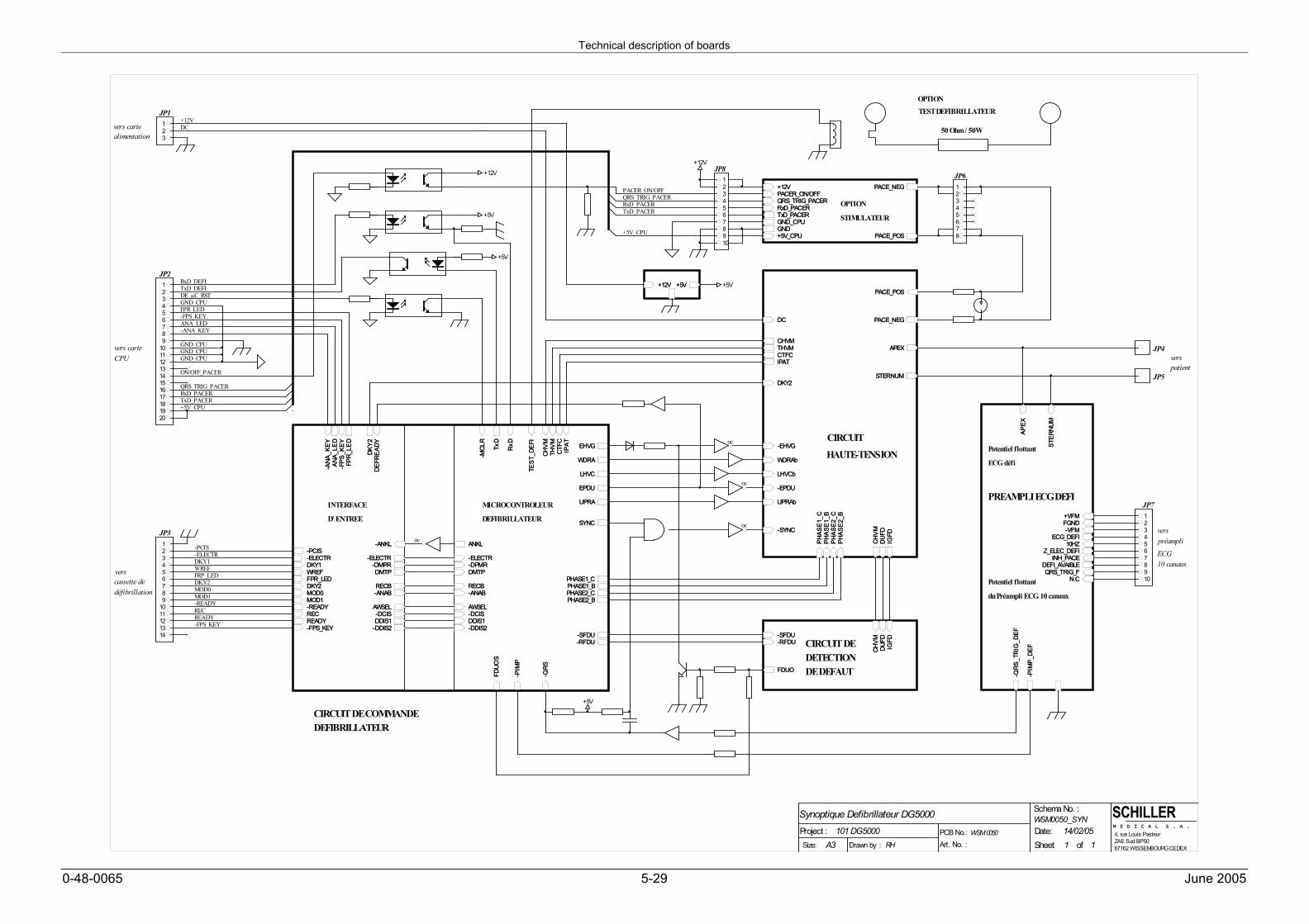
Technical description of boards
0-48-0065 5-29 June 2005
1WSM 0050
1
WSM0050_SYN14/02/05
Size:
Date:Sheet ofA3
Synoptique Defibrillateur DG5000
4, rue Louis PasteurZAE Sud BP5067162 WISSEMBOURG CEDEX
Schema No. :
Project :Art. No. :PCB No.:101 DG5000
Drawn by : RH
SCHILLERM E D I C A L S . A .
123
1234
14
89
10111213
1234567
12345678910
+12VDC
+5V
+5V
-PCIS-ELECTRDKY1WREFFRP_LEDDKY2MOD0MOD1-READYRECREADY-FPS_KEY
-PCIS-ELECTRDKY1WREFFPR_LEDDKY2MOD0MOD1-READY
READYREC
DKY2
DEFR
EADY
-DMPRDMTP
RECB-ANAB
AWSEL-DCISDDIS1
-DDIS2
-ANKL
-FPS_KEY
-ELECTR
-ANA
_KEY
ANA_
LED
-FPS
_KEY
FPR_
LED
-PCIS-ELECTRDKY1WREFFPR_LEDDKY2MOD0MOD1-READY
READYREC
DKY2
DEFR
EADY
-DMPRDMTP
RECB-ANAB
AWSEL-DCISDDIS1
-DDIS2
-ANKL
-FPS_KEY
-ELECTR
-ANA
_KEY
ANA_
LED
-FPS
_KEY
FPR_
LED
INTERFACE
D' ENTREE
JP1
JP2
JP3
IPAT
CTFC
THVM
CHVM
-DPMRDMTP
RECB-ANAB
AWSEL-DCISDDIS1-DDIS2
FDUO
S
-PIM
P
-QRS
EHVG
WDRA
LHVC
EPDU
UPRA
SYNC
PHASE1_CPHASE1_BPHASE2_CPHASE2_B
-SFDU-RFDU
ANKL
RxD
TxD
-MCL
R
-ELECTR
TEST
_DEF
I
IPAT
CTFC
THVM
CHVM
-DPMRDMTP
RECB-ANAB
AWSEL-DCISDDIS1-DDIS2
FDUO
S
-PIM
P
-QRS
EHVG
WDRA
LHVC
EPDU
UPRA
SYNC
PHASE1_CPHASE1_BPHASE2_CPHASE2_B
-SFDU-RFDU
ANKL
RxD
TxD
-MCL
R
-ELECTR
TEST
_DEF
I
MICROCONTROLEUR
DEFIBRILLATEUR
+12V +5V+12V +5V +5V
DC
CHVMTHVMCTFCIPAT
-EHVG
WDRAb
LHVCb
-EPDU
UPRAb
-SYNC
DKY2
PHAS
E1_C
PHAS
E1_B
PHAS
E2_C
PHAS
E2_B
CHVM
DUFD
IGFD
APEX
STERNUM
PACE_POS
PACE_NEGDC
CHVMTHVMCTFCIPAT
-EHVG
WDRAb
LHVCb
-EPDU
UPRAb
-SYNC
DKY2
PHAS
E1_C
PHAS
E1_B
PHAS
E2_C
PHAS
E2_B
CHVM
DUFD
IGFD
APEX
STERNUM
PACE_POS
PACE_NEG
CIRCUIT
HAUTE-TENSION
-SFDU-RFDU
FDUO
CHVM
DUFD
IGFD
-SFDU-RFDU
FDUO
CHVM
DUFD
IGFDCIRCUIT DE
DETECTIONDE DEFAUT
+5V
APEX
STER
NUM
+VFMFGND-VFM
ECG_DEFI10HZ
Z_ELEC_DEFIINH_PACE
DEFI_AVAIBLEQRS_TRIG_F
N.C
-QRS
_TRI
G_D
EF
-PIM
P_DE
FAP
EX
STER
NUM
+VFMFGND-VFM
ECG_DEFI10HZ
Z_ELEC_DEFIINH_PACE
DEFI_AVAIBLEQRS_TRIG_F
N.C
-QRS
_TRI
G_D
EF
-PIM
P_DE
F
Potentiel flottant
ECG défi
PREAMPLI ECG DEFI
Potentiel flottant
du Préampli ECG 10 canaux
JP7
RxD_DEFITxD_DEFIDE_µC_RST
oc
oc
oc
oc
GND_CPU
50 Ohm / 50W
TEST DEFIBRILLATEUR
56789
1011121314151617181920
FPR_LED-FPS_KEYANA_LED-ANA_KEY
21
345678910
JP8
ON/OFF_PACER
QRS_TRIG_PACERRxD_PACERTxD_PACER+5V_CPU
GND_CPUGND_CPUGND_CPU
CIRCUIT DE COMMANDEDEFIBRILLATEUR
+12VPACER_ON/OFFQRS_TRIG_PACERRxD_PACERTxD_PACERGND_CPUGND+5V_CPU
PACE_NEG
PACE_POS
+12VPACER_ON/OFFQRS_TRIG_PACERRxD_PACERTxD_PACERGND_CPUGND+5V_CPU
PACE_NEG
PACE_POS
+12V+12V
PACER_ON/OFFQRS_TRIG_PACERRxD_PACERTxD_PACER
+5V_CPU
2345678
1
JP6
OPTION
OPTION
STIMULATEUR
JP4
JP5
vers carteCPU
vers cartealimentation
cassette dedéfibrillation
vers
verspréampli
ECG
verspatient
10 canaux
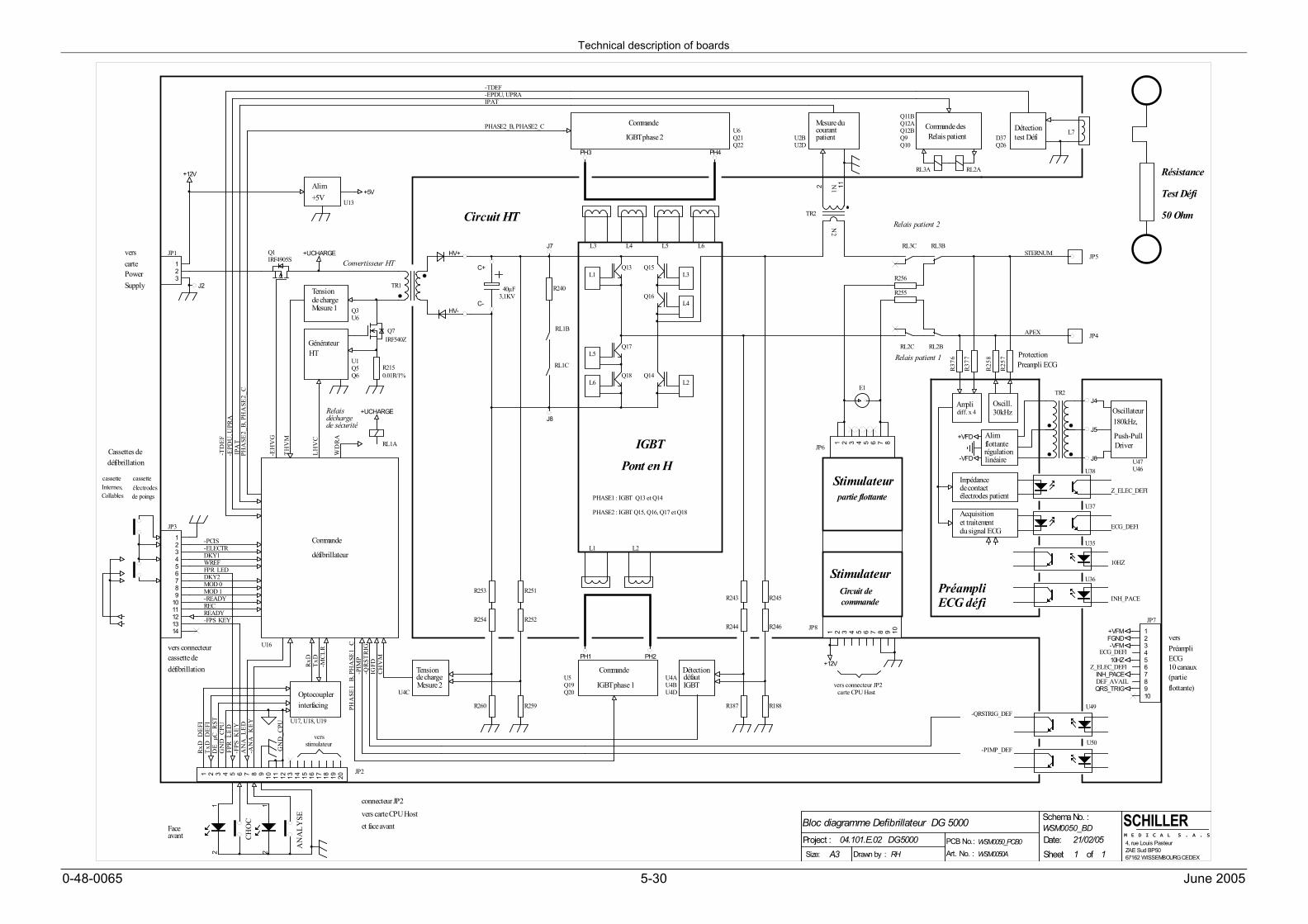
Technical description of boards
0-48-0065 5-30 June 2005
1WSM0050_PCB0
WSM0050A 1
WSM0050_BD21/02/05
Size:
Date:Sheet ofA3
Bloc diagramme Defibrillateur DG 5000
4, rue Louis PasteurZAE Sud BP5067162 WISSEMBOURG CEDEX
Schema No. :
Project :Art. No. :PCB No.:04.101.E.02 DG5000
Drawn by : RH
SCHILLERM E D I C A L S . A . S.
123
JP1
12345678910
JP7
L3 L4 L5 L6
L2L1
2 11N1
N2
TR2
U38
U37
U35
U36
U49
U50
J4
J5
J6
R25
7
R25
8
R37
6
R37
7
APEX
STERNUM
RL2ARL3A
PH3 PH4
40µF
J7
R240
RL1A
RL1B
RL1C
J8
R246R244R254 R252
PH1 PH2
-QRSTRIG_DEF
-PIMP_DEF
Z_ELEC_DEFI
ECG_DEFI
10HZ
INH_PACE
ProtectionPreampli ECG
J2
Convertisseur HT
déchargede sécurité
123456789
1011121314
JP3
HV-
HV+
C+
C-3,1KV
R253 R251R245R243
L7
TR1
1 2 3 4 5 6 7 8 9 10 11 12 13 14 15 16 17 18 19 20
JP2
1 2 3 4 5 6 7 8 9 10
JP8
RL3B
1 2 3 4 5 6 7 8
JP6
RL3C
RL2BRL2C
R255
R256
R260 R259 R187 R188
IGBT
Pont en H
PréampliECG défi
E1
partie flottanteStimulateur
JP5
JP4
Résistance
Test Défi
50 Ohm
Acquisitionet traitementdu signal ECG
Impédance
électrodes patientde contact
Amplidiff. x 4
Oscill.30kHz
Q7IRF540Z
R2150.01R/1%
Q1IRF4905S
GénérateurHT
Tensionde chargeMesure 2
DétectiondéfautIGBT
Commande
IGBT phase 1
Mesure ducourantpatient
Commande desRelais patient
Commande
IGBT phase 2
CH
VM
IGFD
PHA
SE1_
B, P
HA
SE1_
C
Commande
défibrillateur
Détectiontest Défi
Tensionde chargeMesure 1
-PIM
P-Q
RST
RIG
Relais patient 1
Relais patient 2
-EH
VG
TH
VM
LH
VC
WD
RA
Circuit HT
Préampli
10 canaux(partie
vers connecteur
défibrillationcassette de
verscartePowerSupply
vers carte CPU Hostet face avant
+VFD
-VFD
Alimflottanterégulationlinéaire
-TDEF-EPDU, UPRAIPAT
PHASE2_B, PHASE2_C
-TD
EF-E
PDU
, UPR
AIP
AT
PHA
SE2_
B, P
HA
SE2_
C+UCHARGE
Relais +UCHARGE
D37Q26
Q11BQ12AQ12BQ9Q10
U2BU2D
U6Q21Q22
U16
Q6
Q3
Q5U1
U6
U4CQ19Q20
U4BU4A
U4D
U5
+12V
+5VAlim+5V
Oscillateur180kHz,
DriverPush-Pull
U47U46
-PCIS-ELECTRDKY1WREFFPR_LEDDKY2MOD 0MOD 1-READYRECREADY-FPS_KEY
FGND-VFM
+VFM
ECG_DEFI10HZ
Z_ELEC_DEFIINH_PACE
QRS_TRIGDEF_AVAIL
RxD
TxD
-MC
LR
-FPS
_KE
Y
-AN
A_K
EY
FPR
_LE
D
AN
A_L
ED
U13
StimulateurCircuit de commande
versstimulateur
GN
D_C
PU
+12V
vers connecteur JP2carte CPU Host
Q13
Q17
Q18
Q15
Q16
Q14
de poings
vers
ECG
flottante)Optocouplerinterfacing
U17, U18, U19
GN
D_C
PU
RxD
_DE
FIT
xD_D
EFI
DE_
µC_R
ST1
2
Internes,Collables
Cassettes dedéfibrillation
12
CHO
C
AN
AL
YSE
connecteur JP2
Faceavant
PHASE1 : IGBT Q13 et Q14
PHASE2 : IGBT Q15, Q16, Q17 et Q18
TR2
cassette cassetteélectrodes
L1 L3
L2
L4
L5
L6
Technical description of boards
0-48-0065 5-31 June 2005
5.3. CPU BOARD (part no. 3.2852)
This circuit has the part number 3.2652 or WSM0057A.
5.3.1. General
The CPU board is the main board of DG5000. It contains the operating system (Linux), all the associatedapplications, the display and the management of the keypad, the management of all the signals from thesensors and the management of all the inputs and outputs (devices).
The CPU board can be divided into two large parts:- CPU board- ANA part
The CPU board contains the Coldfire microprocessor, the (RAM and flash) memory and devices such asEthernet, USB, the TFT controller, the graph (LPT), the clock (RTC), the sound (OKI + Buzzer) and seriallinks. These serial links enable the board to communicate with the other boards of DG5000(DEFIBRILLATOR and POWER) and the ANA part and the outside environment (RS232).A programmable component (CPLD) is used to decode addresses (selecting the right device), generate resetsignals and some control signals, managing the LPT port, keypad and the rotating button.
The ANA part is based on an Atmel microcontroller that manages the analogue signals of the sensors (Spo2,NIBP, ECG) and the VF data for detecting fibrillation. It communicates all the signals to the Coldfiremicroprocessor by means of a serial link.
The board is supplied with power by the POWER board.
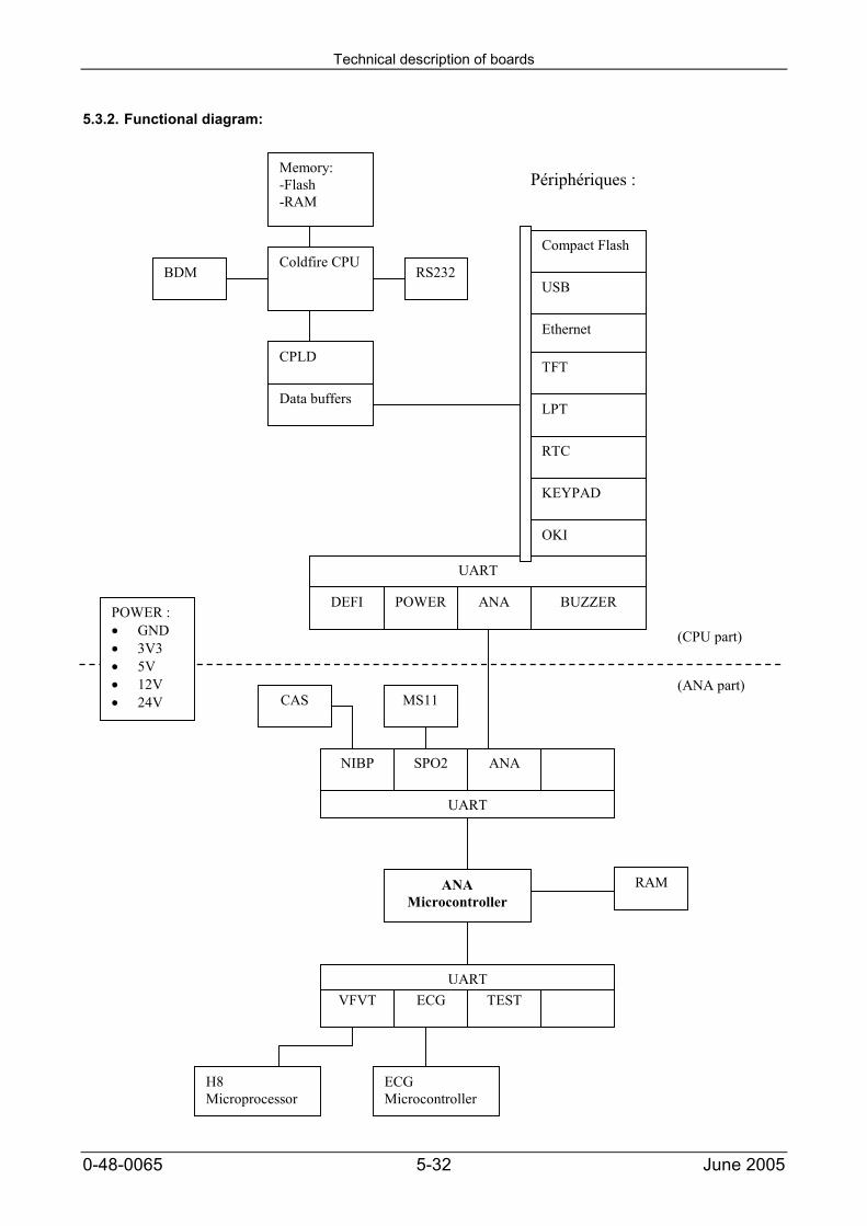
Technical description of boards
0-48-0065 5-32 June 2005
5.3.2. Functional diagram:
TEST
Coldfire CPU
Memory:-Flash-RAM
CPLD
BDM
Compact Flash
USB
Ethernet
TFT
LPT
RTC
BUZZER
OKI
POWER ANADEFI
ANAMicrocontroller
(ANA part)
Data buffers
RS232
KEYPAD
Périphériques :
UART
UART
ANA
RAM
(CPU part)
CAS MS11
ECGMicrocontroller
H8Microprocessor
SPO2NIBP
VFVT
POWER : GND 3V3 5V 12V 24V
ECGUART
Technical description of boards
0-48-0065 5-33 June 2005
5.3.3. Explanation of the various assemblies:
5.3.3.1. CPU board
The CPU is a Motorola Coldfire microprocessor, which executes the different programs (starting up,operating system and applications).
The flash memory contains the bootloader (booting program) and the operating system.
The programs that are running are contained in the RAM (working memory).
The BDM (Background Debug Mode) connector is used to debug and develop applications and hardware. Itis also used for hardware tests.
A console connected to the RS232 output of the CPU shows what the microprocessor is doing and sends itinstructions.
The CPU board access the flash memory and RAM directly. But data buffers are used for access to thedifferent devices.
The CPLD handles address decoding and generates the Chip Select signals that individually activate eachdevice. It also manages the signals of the keypad and the rotating button, the LPT port and the differentcontrol signals.
The compact flash memory contains the applications and configurations (options).
The CPU board of DG5000 has USB and Ethernet connections for communicating with the outside.
A 10"4 TFT screen is interfaced with a flat jumper.
An RTC (Real Time Clock) keeps the time of the device and wakes it up from time to time to perform thetests.
Alarms are generated by a Buzzer and an OKI component saves conversations and plays them back.
A QUAD UART is used for interfacing 4 serial links. These links are used to communicate with the buzzer,the Defibrillator boards (defibrillator status), the power board (battery status) and the ANA part (data fromNIBP, SPO2, ECG, PACE and VF sensors).
5.3.3.2. ANA part
The ANA microcontroller collects the analogue signals from the various sensors (Spo2, NIBP, ECG, PACEand VFVT). It communicates all the signals to the Coldfire microprocessor through a serial link (ANA).
A CAS module is connected to the CPU board to calculate the non-invasive blood pressure (NIBP).
An MS11 module is used to calculate the SPO2 rate and pulse.
Microprocessor H8 is used to process signals and diagnose ventricular fibrillation or ventricular tachycardia.
An ECG microcontroller processes the data from the ECG chain and sends them to the ANA microcontroller.
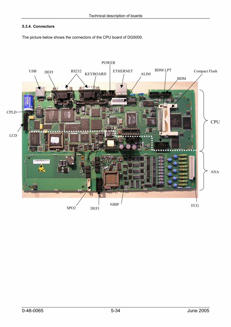
Technical description of boards
0-48-0065 5-34 June 2005
5.3.4. Connectors
The picture below shows the connectors of the CPU board of DG5000.
CPLD
USBKEYBOARD
POWER
ETHERNETALIM
BDM
Compact FlashRS232DEFI
LCD
ECG
ANA
CPU
NIBP
BDM LPT
DEFISPO2
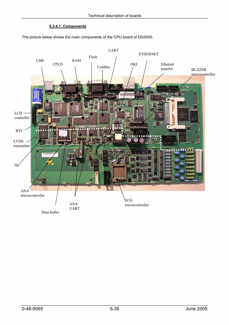
Technical description of boards
0-48-0065 5-35 June 2005
5.3.4.1. Components
The picture below shows the main components of the CPU board of DG5000.
USB RAMFlash
ETHERNET
RTC
Ethernettransfor
LVDStransmitter
Coldfire
LCDcontroller
UART
ANAUART
CPLD
ECGmicrocontroller
OKI
H8
Data buffer
ANAmicrocontroller
BUZZERmicrocontroller

Technical description of boards
0-48-0065 5-36 June 2005
5.4. POWER BOARD (part no. 3.2653)
The part number of this circuit is 3.2653 or WSM0065A.
Technical description of boards
0-48-0065 5-37 June 2005
5.5. UPPER KEYPAD BOARD (part no. WSM0062A)
5.5.1. GeneralThis circuit is located at the top of the front housing. It enables the user to control the device through a foiland to see the proper execution of certain functions by means of indicators. The circuit also includes a CPUinterface function.
5.5.2. Control and displayPressing the On/Off button (S1) switches the ON/OFF signal to the ground and starts the device with the helpof the CPU. Pressing the button once again sets of the device stopping procedure.
Pressing the Charge/Shock button (S2) switches signal -FPS KEY to the ground. Signal - FPS KEY isdetected by the CPU and, depending on the device status, it charges the capacitor or triggers the shock.Three LEDs (LD4, LD5 and LD6) located around the button indicate if the shock is ready.
Pressing the Analyse button (S3) switches signal -ANA KEY to the ground. Signal - ANA KEY is detected bythe CPU and if the three LEDs (LD7, LD8 and LD9) located around the button are illuminated, an analysis isstarted.
The pulses of signal CHARGE LED1 make LD1 flash to show the battery charge.When high, signal DC LED1 switches on LD2 which shows that the external VDC power is present.When high, signal AC LED1 switches on LD3, which shows that the mains power is present.
5.5.3. CPU interfaceAll the signals to the CPU via connector J405M come from the following components:
- Loud speaker (J401M)- Microphone (J402)- Side keypad (J403M)- Rotating selector (J701M)- Recorder (J703)- Backlighting (J704)
Technical description of boards
0-48-0065 5-38 June 2005
5.6. KEYPAD + BATTERY BOARD: (part no. WSM0060A)
5.6.1. GeneralThis circuit is a board made up of three different snap-off circuits. When the circuits are separated, they haveseparate part numbers, namely WSM0060B, WSM0060C and WSM0060D.
5.6.2. DG5000 SIDE KEYPAD PCB: WSM0060BThis circuit has 7 push-buttons and acts as the interface between the user and the machine. The controlsignals go through connector J702M circuit "UPPER KEYPAD" and then to the CPU.
5.6.3. DG5000 BATTERY 1 PCB: WSM0060CThis circuit is screwed to the lower battery tank and is only used as an adapter for battery 1. Contacts JP1,JP2 and JP3 form the connection with the battery and connector J306M is used to connect the assembly tothe power circuit.
5.6.4. DG5000 BATTERY 2 PCB: WSM0060DThis circuit is screwed to the upper battery tank and is the adapter for battery 2 and the interface for thegraph signals.
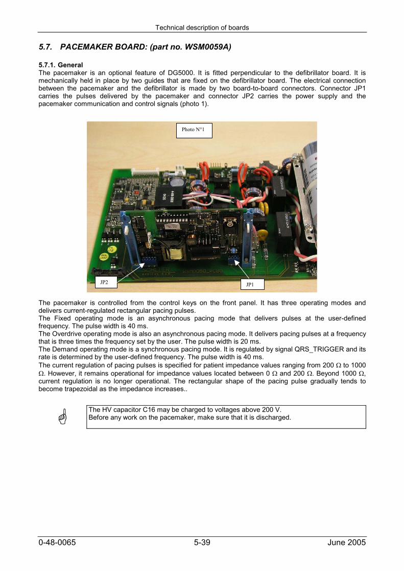
Technical description of boards
0-48-0065 5-39 June 2005
5.7. PACEMAKER BOARD: (part no. WSM0059A)
5.7.1. GeneralThe pacemaker is an optional feature of DG5000. It is fitted perpendicular to the defibrillator board. It ismechanically held in place by two guides that are fixed on the defibrillator board. The electrical connectionbetween the pacemaker and the defibrillator is made by two board-to-board connectors. Connector JP1carries the pulses delivered by the pacemaker and connector JP2 carries the power supply and thepacemaker communication and control signals (photo 1).
Photo N°1
JP1JP2
The pacemaker is controlled from the control keys on the front panel. It has three operating modes anddelivers current-regulated rectangular pacing pulses.The Fixed operating mode is an asynchronous pacing mode that delivers pulses at the user-definedfrequency. The pulse width is 40 ms.The Overdrive operating mode is also an asynchronous pacing mode. It delivers pacing pulses at a frequencythat is three times the frequency set by the user. The pulse width is 20 ms.The Demand operating mode is a synchronous pacing mode. It is regulated by signal QRS_TRIGGER and itsrate is determined by the user-defined frequency. The pulse width is 40 ms.The current regulation of pacing pulses is specified for patient impedance values ranging from 200 to 1000. However, it remains operational for impedance values located between 0 and 200 . Beyond 1000 ,current regulation is no longer operational. The rectangular shape of the pacing pulse gradually tends tobecome trapezoidal as the impedance increases..
The HV capacitor C16 may be charged to voltages above 200 V.Before any work on the pacemaker, make sure that it is discharged.
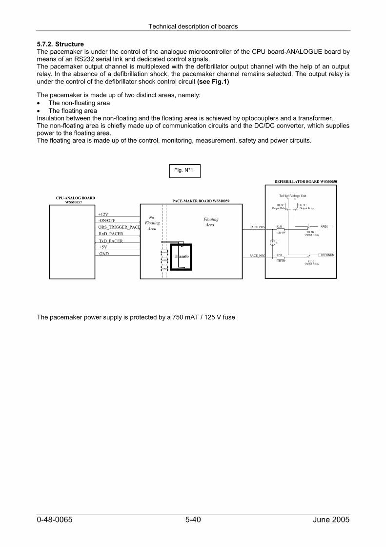
Technical description of boards
0-48-0065 5-40 June 2005
5.7.2. StructureThe pacemaker is under the control of the analogue microcontroller of the CPU board-ANALOGUE board bymeans of an RS232 serial link and dedicated control signals.The pacemaker output channel is multiplexed with the defibrillator output channel with the help of an outputrelay. In the absence of a defibrillation shock, the pacemaker channel remains selected. The output relay isunder the control of the defibrillator shock control circuit (see Fig.1)
The pacemaker is made up of two distinct areas, namely: The non-floating area The floating areaInsulation between the non-floating and the floating area is achieved by optocouplers and a transformer.The non-floating area is chiefly made up of communication circuits and the DC/DC converter, which suppliespower to the floating area.The floating area is made up of the control, monitoring, measurement, safety and power circuits.
OPTO
OPTO
OPTO
Transfo
RL2BOutput Relay
RL3BOutput Relay
RL3COutput Relay
RL2COutput Relay
+12V
GND
QRS_TRIGGER_PACE
TxD_PACER+5V
RxD_PACER
-ON/OFFPACE_POS
PACE_NEG
R255
10R/1W
R256
10R/1W
E1
APEX
STERNUM
To High Voltage Unit
DEFIBRILLATOR BOARD WSM0050
PACE-MAKER BOARD WSM0059
NoFloating
Area
FloatingArea
CPU-ANALOG BOARDWSM0057
The pacemaker power supply is protected by a 750 mAT / 125 V fuse.
Fig. N°1
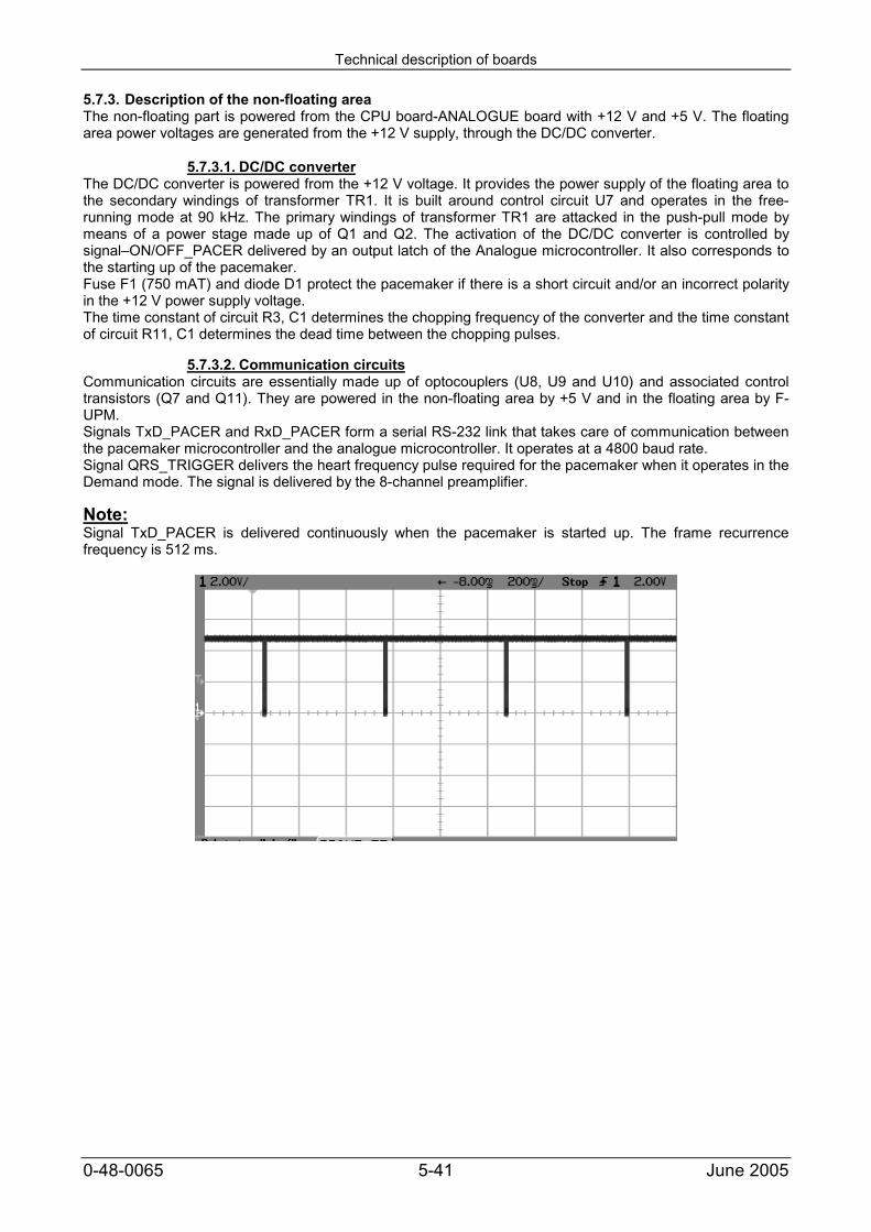
Technical description of boards
0-48-0065 5-41 June 2005
5.7.3. Description of the non-floating areaThe non-floating part is powered from the CPU board-ANALOGUE board with +12 V and +5 V. The floatingarea power voltages are generated from the +12 V supply, through the DC/DC converter.
5.7.3.1. DC/DC converterThe DC/DC converter is powered from the +12 V voltage. It provides the power supply of the floating area tothe secondary windings of transformer TR1. It is built around control circuit U7 and operates in the free-running mode at 90 kHz. The primary windings of transformer TR1 are attacked in the push-pull mode bymeans of a power stage made up of Q1 and Q2. The activation of the DC/DC converter is controlled bysignal–ON/OFF_PACER delivered by an output latch of the Analogue microcontroller. It also corresponds tothe starting up of the pacemaker.Fuse F1 (750 mAT) and diode D1 protect the pacemaker if there is a short circuit and/or an incorrect polarityin the +12 V power supply voltage.The time constant of circuit R3, C1 determines the chopping frequency of the converter and the time constantof circuit R11, C1 determines the dead time between the chopping pulses.
5.7.3.2. Communication circuitsCommunication circuits are essentially made up of optocouplers (U8, U9 and U10) and associated controltransistors (Q7 and Q11). They are powered in the non-floating area by +5 V and in the floating area by F-UPM.Signals TxD_PACER and RxD_PACER form a serial RS-232 link that takes care of communication betweenthe pacemaker microcontroller and the analogue microcontroller. It operates at a 4800 baud rate.Signal QRS_TRIGGER delivers the heart frequency pulse required for the pacemaker when it operates in theDemand mode. The signal is delivered by the 8-channel preamplifier.
Note:Signal TxD_PACER is delivered continuously when the pacemaker is started up. The frame recurrencefrequency is 512 ms.
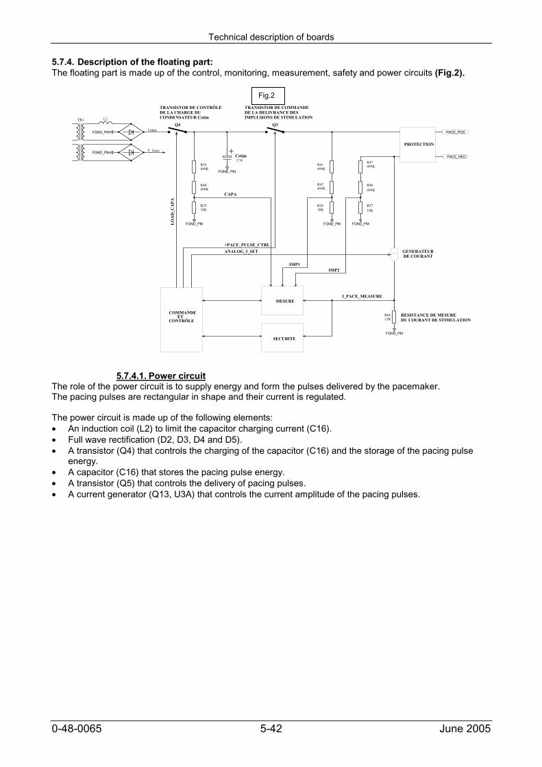
Technical description of boards
0-48-0065 5-42 June 2005
5.7.4. Description of the floating part:The floating part is made up of the control, monitoring, measurement, safety and power circuits (Fig.2).
TR1
FGND_PM
FGND_PM F_Uaux
Ustim
C16R39499K
R40499K
R41499K
R42499K
R2510K
R2610K
R2710K
R48499K
R47499K
PACE_NEG
PACE_POS
R6615R
FGND_PM
FGND_PMFGND_PMFGND_PM
FGND_PM
COMMANDE
CONTRÔLE
SECURITE
MESURE
ET
LO
AD
_CA
PA
CAPA
+PACE_PULSE_CTRLANALOG_I_SET
IMP1IMP2
GENERATEURDE COURANT
RESISTANCE DE MESUREDU COURANT DE STIMULATION
Cstim
TRANSISTOR DE CONTRÔLEDE LA CHARGE DUCONDENSATEUR Cstim
TRANSISTOR DE COMMANDEDE LA DELIVRANCE DESIMPULSIONS DE STIMULATION
Q4 Q3L2
I_PACE_MEASURE
PROTECTION
5.7.4.1. Power circuitThe role of the power circuit is to supply energy and form the pulses delivered by the pacemaker.The pacing pulses are rectangular in shape and their current is regulated.
The power circuit is made up of the following elements: An induction coil (L2) to limit the capacitor charging current (C16). Full wave rectification (D2, D3, D4 and D5). A transistor (Q4) that controls the charging of the capacitor (C16) and the storage of the pacing pulse
energy. A capacitor (C16) that stores the pacing pulse energy. A transistor (Q5) that controls the delivery of pacing pulses. A current generator (Q13, U3A) that controls the current amplitude of the pacing pulses.
Fig.2
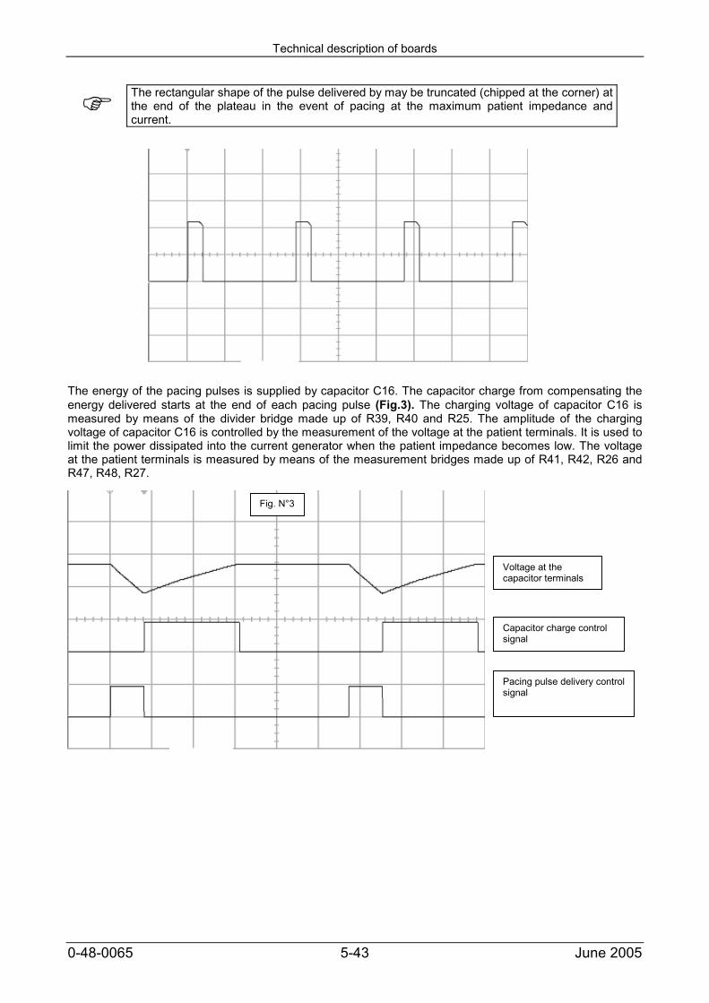
Technical description of boards
0-48-0065 5-43 June 2005
The rectangular shape of the pulse delivered by may be truncated (chipped at the corner) atthe end of the plateau in the event of pacing at the maximum patient impedance andcurrent.
The energy of the pacing pulses is supplied by capacitor C16. The capacitor charge from compensating theenergy delivered starts at the end of each pacing pulse (Fig.3). The charging voltage of capacitor C16 ismeasured by means of the divider bridge made up of R39, R40 and R25. The amplitude of the chargingvoltage of capacitor C16 is controlled by the measurement of the voltage at the patient terminals. It is used tolimit the power dissipated into the current generator when the patient impedance becomes low. The voltageat the patient terminals is measured by means of the measurement bridges made up of R41, R42, R26 andR47, R48, R27.
Voltage at thecapacitor terminals
Capacitor charge controlsignal
Pacing pulse delivery controlsignal
Fig. N°3
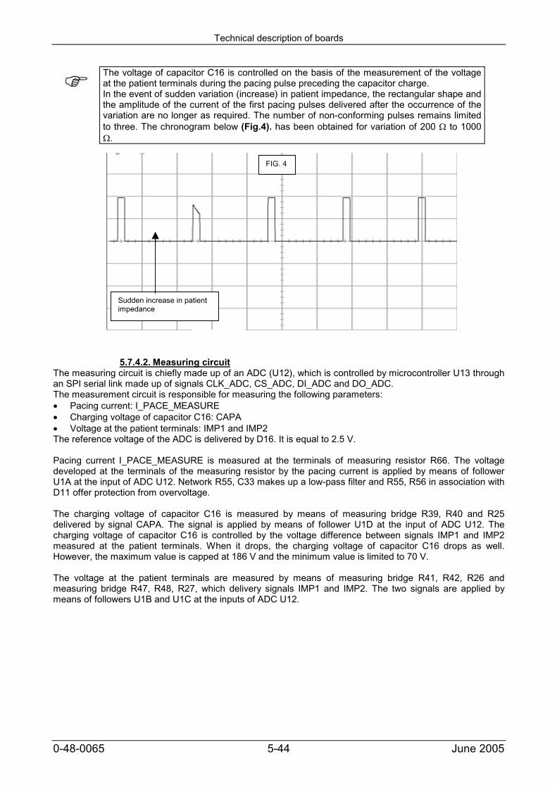
Technical description of boards
0-48-0065 5-44 June 2005
The voltage of capacitor C16 is controlled on the basis of the measurement of the voltageat the patient terminals during the pacing pulse preceding the capacitor charge.In the event of sudden variation (increase) in patient impedance, the rectangular shape andthe amplitude of the current of the first pacing pulses delivered after the occurrence of thevariation are no longer as required. The number of non-conforming pulses remains limitedto three. The chronogram below (Fig.4). has been obtained for variation of 200 to 1000.
5.7.4.2. Measuring circuitThe measuring circuit is chiefly made up of an ADC (U12), which is controlled by microcontroller U13 throughan SPI serial link made up of signals CLK_ADC, CS_ADC, DI_ADC and DO_ADC.The measurement circuit is responsible for measuring the following parameters: Pacing current: I_PACE_MEASURE Charging voltage of capacitor C16: CAPA Voltage at the patient terminals: IMP1 and IMP2The reference voltage of the ADC is delivered by D16. It is equal to 2.5 V.
Pacing current I_PACE_MEASURE is measured at the terminals of measuring resistor R66. The voltagedeveloped at the terminals of the measuring resistor by the pacing current is applied by means of followerU1A at the input of ADC U12. Network R55, C33 makes up a low-pass filter and R55, R56 in association withD11 offer protection from overvoltage.
The charging voltage of capacitor C16 is measured by means of measuring bridge R39, R40 and R25delivered by signal CAPA. The signal is applied by means of follower U1D at the input of ADC U12. Thecharging voltage of capacitor C16 is controlled by the voltage difference between signals IMP1 and IMP2measured at the patient terminals. When it drops, the charging voltage of capacitor C16 drops as well.However, the maximum value is capped at 186 V and the minimum value is limited to 70 V.
The voltage at the patient terminals are measured by means of measuring bridge R41, R42, R26 andmeasuring bridge R47, R48, R27, which delivery signals IMP1 and IMP2. The two signals are applied bymeans of followers U1B and U1C at the inputs of ADC U12.
Sudden increase in patientimpedance
FIG. 4
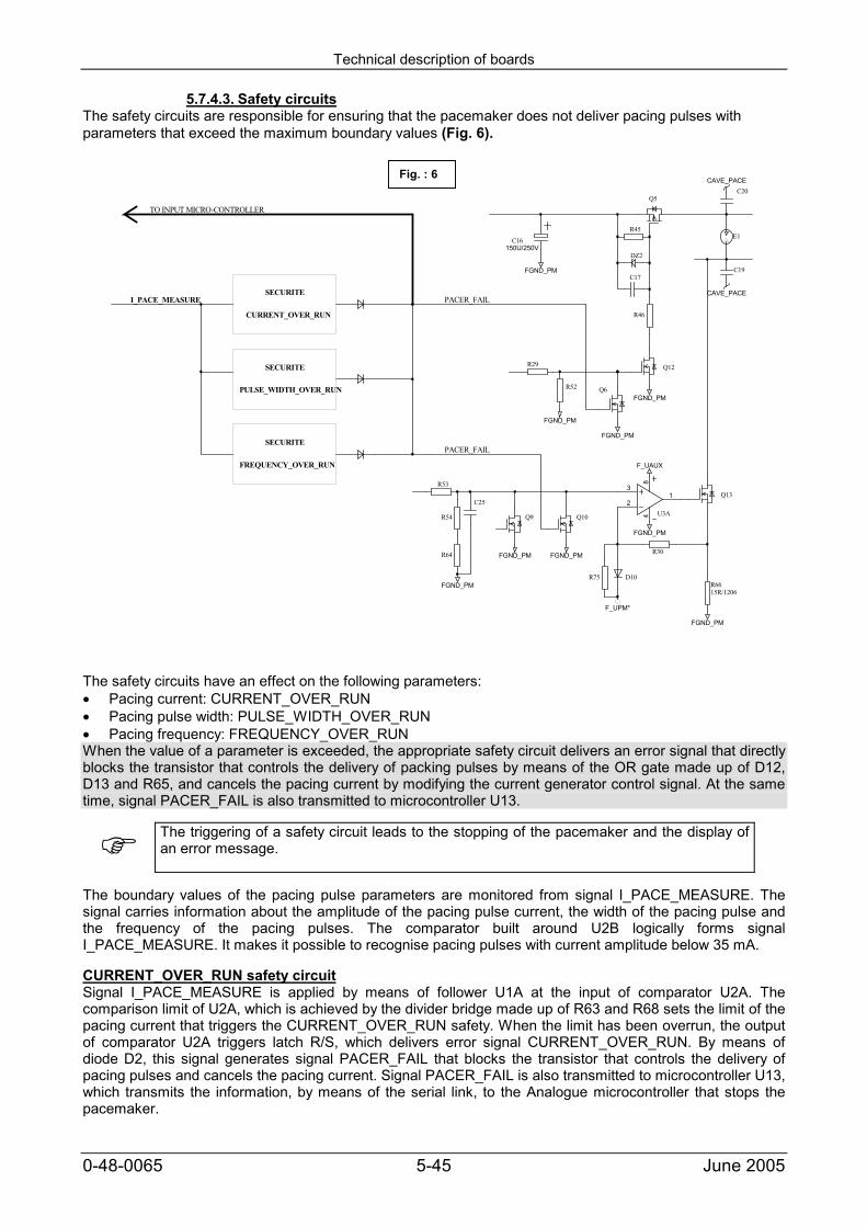
Technical description of boards
0-48-0065 5-45 June 2005
5.7.4.3. Safety circuitsThe safety circuits are responsible for ensuring that the pacemaker does not deliver pacing pulses withparameters that exceed the maximum boundary values (Fig. 6).
F_UAUX
R29
R52
R54
R53
Q6
Q10
FGND_PM
FGND_PM
FGND_PM
FGND_PM
FGND_PM
3
21
84 U3A
Q12
Q13
C17
R46
DZ2
C25
FGND_PM
Q9
FGND_PMR64
R45
D10
F_UPM*
R30
R75
Q5C20
C19
CAVE_PACE
CAVE_PACE
E1
FGND_PM
C16150U/250V
R6615R/1206
FGND_PM
CURRENT_OVER_RUN
SECURITE
FREQUENCY_OVER_RUN
SECURITE
PULSE_WIDTH_OVER_RUN
SECURITEI_PACE_MEASURE PACER_FAIL
PACER_FAIL
TO INPUT MICRO-CONTROLLER
The safety circuits have an effect on the following parameters: Pacing current: CURRENT_OVER_RUN Pacing pulse width: PULSE_WIDTH_OVER_RUN Pacing frequency: FREQUENCY_OVER_RUNWhen the value of a parameter is exceeded, the appropriate safety circuit delivers an error signal that directlyblocks the transistor that controls the delivery of packing pulses by means of the OR gate made up of D12,D13 and R65, and cancels the pacing current by modifying the current generator control signal. At the sametime, signal PACER_FAIL is also transmitted to microcontroller U13.
The triggering of a safety circuit leads to the stopping of the pacemaker and the display ofan error message.
The boundary values of the pacing pulse parameters are monitored from signal I_PACE_MEASURE. Thesignal carries information about the amplitude of the pacing pulse current, the width of the pacing pulse andthe frequency of the pacing pulses. The comparator built around U2B logically forms signalI_PACE_MEASURE. It makes it possible to recognise pacing pulses with current amplitude below 35 mA.
CURRENT_OVER_RUN safety circuitSignal I_PACE_MEASURE is applied by means of follower U1A at the input of comparator U2A. Thecomparison limit of U2A, which is achieved by the divider bridge made up of R63 and R68 sets the limit of thepacing current that triggers the CURRENT_OVER_RUN safety. When the limit has been overrun, the outputof comparator U2A triggers latch R/S, which delivers error signal CURRENT_OVER_RUN. By means ofdiode D2, this signal generates signal PACER_FAIL that blocks the transistor that controls the delivery ofpacing pulses and cancels the pacing current. Signal PACER_FAIL is also transmitted to microcontroller U13,which transmits the information, by means of the serial link, to the Analogue microcontroller that stops thepacemaker.
Fig. : 6
Technical description of boards
0-48-0065 5-46 June 2005
PULSE_WIDTH_OVER_RUN safety circuitSignal I_PACE_MEASURE is applied by means of follower U1A at the input of comparator U2B, which formssignal I_PACE_MEASURE, which is used to apply the pacing pulses with currents that are as low as 25 mA.The signal delivered by the output of comparator U2B attacks its rising edge at the input of monostable U6A.U6A delivers an active pulse with the low status that sets the maximum limit of the pacing pulse width. Thepulse is applied simultaneously with the signal delivered by comparator U2B to logical gate U4B. If the pacingpulse duration exceeds the duration of the pulse generated by monostable U6A, the output of logical gateU4B switches to low and triggers latch R/S. At its PULSE_WIDTH_OVER_RUN output, the latch delivers theerror signal PACER_FAIL, which blocks the transistor that controls the delivery of pacing pulses and cancelsthe pacing current by modifying the control signal of the current generator. At the same time, signalPACER_FAIL is also transmitted to microcontroller U13, which transmits the information by means of theserial link to the Analogue microcontroller that controls the stopping of the pacemaker.Latch R/S is reinitialised by signal–FOR_INHIB, which is active when low.
If there is a fault that affects the pacing current by reducing its amplitude beyond 25 mA, thePULSE_WIDTH_OVER_RUN and FREQUENCY_OVER_RUN safety circuits cease tooperate.
FREQUENCY_OVER_RUN safety circuitSignal I_PACE_MEASURE is applied by means of follower U1A at the input of comparator U2B, which formssignal I_PACE_MEASURE that is used to apply pacing pulses with currents as low as 25 mA. The signaldelivered by the output of comparator U2B attacks the input of monostable U6B on its falling edge. U6Bdelivers a pulse that is active when high, which sets the maximum limit of the pacing frequency. The pulse isapplied simultaneously with the signal delivered by comparator U2B to logical gate U5C. If the durationbetween two consecutive pacing pulses is smaller than the duration of the pulse delivered by monostableU6B, the output from logical gate U5C switches to low and triggers latch R/S. At itsFREQUENCY_OVER_RUN output, latch R/S delivers error signal PACER_FAIL that blocks the transistorthat controls the delivery of pacing pulses and cancels the pacing current by affecting the control signal of thecurrent generator. At the same time, signal PACER_FAIL is also transmitted to microcontroller U13. U13transmits the information by means of the serial link to the Analogue microcontroller that stops thepacemaker.Latch R/S is reinitialised by signal –FOR_INHIB that is active when low.
The OVER_RUN_FREQUENCY safety circuit is disabled when the pacemaker is inOverdrive mode.Such disabling is activated by means of signal –FOR_INHIB. The other safety circuitsremain operational.
The RESET signal generated by voltage supervisor U14 also affects signal PACER_FAIL in the same way asthe three safety circuits. However, the RESET pulse does not lead to the stopping of the pacemaker. It onlyprevents the delivery of a parasite pulse during the pacemaker starting and stopping phases.
Technical description of boards
0-48-0065 5-47 June 2005
5.7.4.4. Control and monitoring circuitThe control and monitoring circuit is chiefly made up of microcontroller U13. It operates with an 11,0592 MHzclock delivered by oscillator Q14. It delivers the various control and monitoring signals and receives the statussignals from the safety circuits. It also supports communication signals with the ADC, the Analoguemicrocontroller and the 8-channel preamplifier.
Signals CLK_ADC, CS_ADC, DI_ADC and DO_ADC form a synchronous serial link that communicateswith ADC U12.
Signals RxD_PACER and TxD_PACER form an RS232 serial link that communicates with the Analoguemicrocontroller.
Signal QRS_TRIGGER_FLOAT delivers to microcontroller U13 the QRS synchronisation information frothe Demand operating mode.
Signal LOAD_CAPA controls and monitors the charging of capacitor C16. Transistor Q3 translates thelevel between control signal LOAD_CAPA and transistor Q4 that controls the charging of capacitor C16.
Signal PACE_PULSE_CTRL controls the delivery of pacing pulses. Transistor Q12 translates the levelbetween control signal PACE_PULSE_CTRL and transistor Q5 that controls the delivery of pacingpulses.
Signal –PACE_PULSE_CTRL affects the current generator adjustment voltage by means of transistorQ9. During the pacing pulse delivery phase, transistor Q9 remains blocked and has no effect on thecurrent generator adjustment voltage. Away from the pacing pulse delivery phase, transistor Q9 issaturated and forces the current generator adjustment voltage to zero.
Signal –FOR_INHIB delivered by microcontroller U13 is used as the reset signal of latches R/S of thesafety circuits. It also controls the disabling of the FREQUENCY_OVER_RUN safety circuit when thepacemaker is operating in Demand mode.
Error signal PACER_FAIL delivered by the safety circuits informs microcontroller U13 of the triggering ofa safety circuit.
Signal PWM_I_SET delivered by microcontroller U13 controls the pacing pulse current. It acts bymodulating the pulse width. The low-pass filter built around U3B generates analogue signalANALOG_I_SET from the pulse-width modulated signal for adjusting the current generator current. Thetime constant by R53, R54, R64 and C25 controls the rising edge of the pacing pulse current.
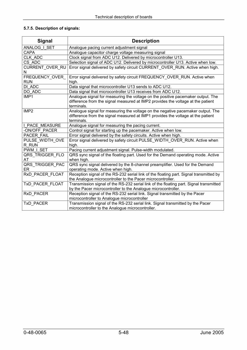
Technical description of boards
0-48-0065 5-48 June 2005
5.7.5. Description of signals:
Signal DescriptionANALOG_I_SET Analogue pacing current adjustment signalCAPA Analogue capacitor charge voltage measuring signalCLK_ADC Clock signal from ADC U12. Delivered by microcontroller U13.CS_ADC Selection signal of ADC U12. Delivered by microcontroller U13. Active when low.CURRENT_OVER_RUN
Error signal delivered by safety circuit CURRENT_OVER_RUN. Active when high.
FREQUENCY_OVER_RUN
Error signal delivered by safety circuit FREQUENCY_OVER_RUN. Active whenhigh.
DI_ADC Data signal that microcontroller U13 sends to ADC U12.DO_ADC Data signal that microcontroller U13 receives from ADC U12.IMP1 Analogue signal for measuring the voltage on the positive pacemaker output. The
difference from the signal measured at IMP2 provides the voltage at the patientterminals.
IMP2 Analogue signal for measuring the voltage on the negative pacemaker output. Thedifference from the signal measured at IMP1 provides the voltage at the patientterminals.
I_PACE_MEASURE Analogue signal for measuring the pacing current.-ON/OFF_PACER Control signal for starting up the pacemaker. Active when low.PACER_FAIL Error signal delivered by the safety circuits. Active when high.PULSE_WIDTH_OVER_RUN
Error signal delivered by safety circuit PULSE_WIDTH_OVER_RUN. Active whenhigh.
PWM_I_SET Pacing current adjustment signal. Pulse-width modulated.QRS_TRIGGER_FLOAT
QRS sync signal of the floating part. Used for the Demand operating mode. Activewhen high.
QRS_TRIGGER_PACER
QRS sync signal delivered by the 8-channel preamplifier. Used for the Demandoperating mode. Active when high.
RxD_PACER_FLOAT Reception signal of the RS-232 serial link of the floating part. Signal transmitted bythe Analogue microcontroller to the Pacer microcontroller.
TxD_PACER_FLOAT Transmission signal of the RS-232 serial link of the floating part. Signal transmittedby the Pacer microcontroller to the Analogue microcontroller.
RxD_PACER Reception signal of the RS-232 serial link. Signal transmitted by the Pacermicrocontroller to Analogue microcontroller
TxD_PACER Transmission signal of the RS-232 serial link. Signal transmitted by the Pacermicrocontroller to the Analogue microcontroller.
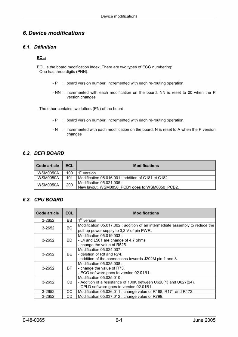
Device modifications
0-48-0065 6-1 June 2005
6. Device modifications
6.1. Définition
ECL:
ECL is the board modification index. There are two types of ECG numbering:- One has three digits (PNN).
- P : board version number, incremented with each re-routing operation
- NN : incremented with each modification on the board. NN is reset to 00 when the Pversion changes
- The other contains two letters (PN) of the board
- P : board version number, incremented with each re-routing operation.
- N : incremented with each modification on the board. N is reset to A when the P versionchanges
6.2. DEFI BOARD
Code article ECL Modifications
WSM0050A 100 1st versionWSM0050A 101 Modification 05.016.001 : addition of C181 et C182.
WSM0050A 200 Modification 05.021.005 :New layout, WSM0050_PCB1 goes to WSM0050_PCB2.
6.3. CPU BOARD
Code article ECL Modifications
3-2652 BB 1st version
3-2652 BCModification 05.017.002 : addition of an intermediate assembly to reduce thepull-up power supply to 3,3 V of pin PWR.
3-2652 BDModification 05.019.003 :- L4 and L501 are change of 4,7 ohms- change the value of R525.
3-2652 BEModification 05.024.007 :- deletion of R8 and R74.- addition of the connections towards J202M pin 1 and 3.
3-2652 BFModification 05.025.008 :- change the value of R73.- ECG software goes to version 02.01B1.
3-2652 CBModification 05.035.010 :- Addition of a resistance of 100K between U620(1) and U627(24).- CPLD software goes to version 02.01B1.
3-2652 CC Modification 05.036.011 : change value of R168, R171 and R172.3-2652 CD Modification 05.037.012 : change value of R799.
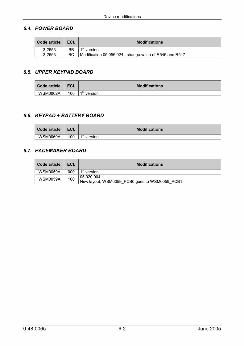
Device modifications
0-48-0065 6-2 June 2005
6.4. POWER BOARD
Code article ECL Modifications
3-2653 BB 1st version3-2653 BC Modification 05.056.024 : change value of R546 and R547
6.5. UPPER KEYPAD BOARD
Code article ECL Modifications
WSM0062A 100 1st version
6.6. KEYPAD + BATTERY BOARD
Code article ECL Modifications
WSM0060A 100 1st version
6.7. PACEMAKER BOARD
Code article ECL Modifications
WSM0059A 000 1st version
WSM0059A 100 05.020.004 :New layout, WSM0059_PCB0 goes to WSM0059_PCB1.
Diagrams and layout drawings
0-48-0065 7-1 June 2005
7. Diagrams and layout drawings7.1. General synoptic
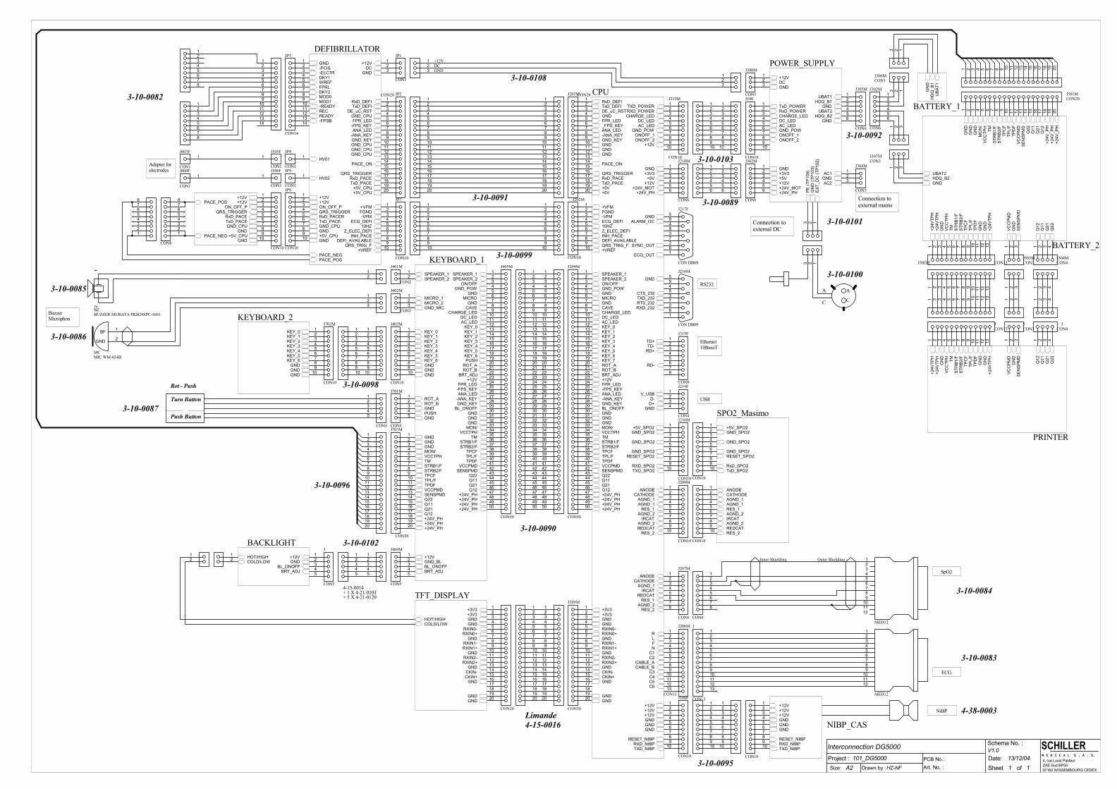
1 1
V1.013/12/04
Size:
Date:Sheet ofA2
Interconnection DG5000
4, rue Louis PasteurZAE Sud BP5067162 WISSEMBOURG CEDEX
Schema No. :
Project :Art. No. :PCB No.:101_DG5000
Drawn by :HZ-NF
SCHILLERM E D I C A L S . A . S.
GND-PCIS
DKY1WREF
HV01
DKY2MOD0MOD1-READY
READYREC
HV02
RxD_DEFITxD_DEFI
DE_uC_RST
DCGND
GND_CPU
+VREF
ECG_DEFI
DEFI_AVAILABLE
Z_ELEC_DEFIINH_PACE
10HZ
+VFMFGND-VFM
QRS_TRIG_F
+12V
-ELCTR
FPRL
-FPSB
-ANA_KEYANA_LED
-FPS_KEYFPR_LED
GND_KEY
PACE_ON
TxD_PACERxD_PACE
QRS_TRIGGER
+5V_CPU+12V+12VON_OFF_PQRS_TRIGGERRxD_PACERTxD_PACEGND_CPUGND
GND+5V_CPU
PACE_NEGPACE_POS
+5V_CPU
GND_CPUGND_CPUGND_CPU
DEFIBRILLATOR
123456789
101112
MED12
123456789
101112
MED12
12345678
1J105F
CON1
1J106F
CON1
12345678
1JP4
CON1
1JP5
CON1
Adapter forelectrodes
RLFN
C1C2
CABLE_ACABLE_B
C3C4C5C6
10HZ
INH_PACEZ_ELEC_DEFI
+VFMFGND-VFMECG_DEFI
DEFI_AVAILABLEQRS_TRIG_F+VREF
RxD_DEFITxD_DEFIDE_uC_RSTGND
TD+TD-
RD+
D-V_USB
GNDD+
RD-
CTS_232TXD_232RTS_232
ANODECATHODE
AGND_1IRCAT
REDCAT
AGND_2
CATHODEAGND_1
AGND_2
REDCATAGND_2
RXD_232
ANODE
TXD_POWERRXD_POWERCHARGE_LED
DC_LEDAC_LED
GND_POWONOFF_1ONOFF_2
GND
GNDALARM_OC
+24V_MOT
SYNC_OUT
ECG_OUT
AGND_1
IRCAT
+5V_SPO2GND_SPO2
GND_SPO2
GND_SPO2RESET_SPO2
RXD_SPO2TXD_SPO2
+24V_PH
+12V+5V
GND+3V3
GND
GNDMICRO
SPEAKER_2SPEAKER_1
ON/OFFGND_POW
AC_LEDDC_LEDCHARGE_LED
BL_ONOFFGND
BRT_ADJ
+12V+12V
GNDGND
RESET_NIBPRXD_NIBPTXD_NIBP
KEY_0
KEY_2KEY_3KEY_4KEY_5KEY_6KEY_7
KEY_1
ROT_AROT_B
GND
+3V3+3V3
MON/GND
RXIN0-RXIN0+GNDRXIN1-RXIN1+GNDRXIN2-RXIN2+GNDCKIN-CKIN+
GND
GNDGND
+12VFPR_LED
-ANA_KEYGND_KEY
-FPS_KEYANA_LED
FPR_LED_FPS_KEYANA_LED-ANA_KEYGND_KEY
+24V_PH
+24V_PH
GND
VCCTPHTMSTRB1/FSTRB2/FTPCFTPL/FTPDF
GND
+24V_PH
VCCPMDSENSPMD
Q12
Q11Q21
Q22
PACE_ON
TxD_PACERxD_PACEQRS_TRIGGER
+5V
GNDGNDGND
+5V
+12V
+12VGND
RES_1
RES_2
RES_2
RES_1
CAVE
+24V_PH
CPU
ANODECATHODE
AGND_2IRCAT
REDCATAGND_2
RxD_SPO2TxD_SPO2
RESET_SPO2
+5V_SPO2GND_SPO2
GND_SPO2
GND_SPO2
AGND_1AGND_1RES_1
RES_2
SPO2_Masimo
123456789
10
JP7
CON10
12345678910
J202M
CON10
GN
D (T
P103
)EX
T_D
C (T
P102
)
AC2
AC1
UBAT2
GND
UBAT1
GND
GND
+24V_MOT
+5V+12V
GND
ONOFF_1
AC_LED
CHARGE_LED
DC
GND_POW
RxD_POWERTxD_POWER
+12V
ONOFF_2
DC_LED
+24V_PH
+3V3GND
HDQ_B1
HDQ_B2
PE (T
P104
)
POWER_SUPPLY
Connection toexternal mains
Connection toexternal DC
UBA
T1
GN
DH
DQ
_B1
BATTERY_1
594837261
J216M
CON DB09
1234
J214F
CON4
RS232
USB
Ethernet10BaseT
12345678
J215F
CON8
DCGND
123456789
10
12345678910
123
JP1
CON3
123
123
123
J300M
CON3
+12V
BuzzerMicrophon
123456
J302M
CON6
123456
ECG
SpO2
NiBP
TXD_NIBPRXD_NIBPRESET_NIBP
+12V
GND
+12V
GNDGND+12V
NIBP_CAS
12345678910
CON10
12345678910
123456789
10
123456789
10
J108F
CON10
123456789
10
J209M
CON10
12345678910
CON10
123456789
10
J210M
CON10
12345678910
CON10
BRT_ADJ
GND_BLBL_ONOFF
+12V
SPEAKER_1SPEAKER_2
MICRO_1MICRO_2
BRT_ADJ
GND
+12V
BL_ONOFF
FPR_LED-FPS_KEYANA_LED
-ANA_KEY
CHARGE_LEDDC_LEDAC_LED
GND
ON/OFFGND_POW
SPEAKER_1SPEAKER_2
MICROGND
CAVEGND_MIC
GND_KEY
KEY_1KEY_2KEY_3KEY_4
GND
KEY_5KEY_6
KEY_0
GND ROT_AROT_B
GND
KEY_2KEY_3
KEY_6PUSH
KEY_0
KEY_4KEY_5
KEY_1
GNDMON/
VCCTPHTM
STRB1/FSTRB2/F
TPCFTPL/FTPDF
VCCPMDSENSPMD
Q11
Q12Q21
Q22
+24V_PH+24V_PH+24V_PH+24V_PH
ROT_AROT_B
PUSHGND
GNDGND
TMSTRB1/FSTRB2/FTPCFTPL/FTPDFVCCPMDSENSPMD
Q11
Q12Q21
Q22
+24V_PH
VCCTPH
+24V_PH
GND
GND
+24V_PH
MON/
GND
KEYBOARD_112
J401M
CON2
12
12345
J404M
CON5
KEY_1KEY_2KEY_3KEY_4KEY_5KEY_6
KEY_0
GNDGNDGND
KEYBOARD_2
BRT_ADJ
GNDBL_ONOFF
+12VHOT/HIGHCOLD/LOW
BACKLIGHT12345
12345
12345
J
CON5
12
BZBUZZER MURATA PKB24SPC-3601
BF 1
GND 2
MCMIC WM-034B
123456789
1011121314151617181920
CON20
123456789
1011121314151617181920
1234567891011121314151617181920
594837261
J217F
CON DB09
HOT/HIGHCOLD/LOW
+3V3+3V3GNDGND
RXIN0-RXIN0+
GNDRXIN1-RXIN1+
GNDRXIN2-RXIN2+
GNDCKIN-CKIN+
GND
GNDGND
TFT_DISPLAY
12
12
123
123
J402M
CON3
Outer ShieldingInner Shielding
1234567891011121314
JP3
CON14
123456789
1011121314
1J603F
CON1
1J604F
CON1
123456
J218M
CON6
123456
1 2 3 1 2 3 41 2 3 4 5 6 7 8 9 10 11 12 13
1 2 3
JCON3
1 2 3 4
1 2 3 4 5 6 7 8 9 10 11 12 13
JCON13
1 2 3
1 2 3 4
JCON4
1 2 3 4 5 6 7 8 9 10 11 12 13
+24V
TPH
+24V
TPH
GN
DVC
CTP
HTM
STR
B1/F
STR
B2/F
TPC
FTP
L/F
TPD
FG
ND
GN
D+2
4VTP
H
GN
DVC
CPM
D
SEN
SPM
D
Q12
Q11
Q21
Q22
PRINTER
123
123
J304M
CON3
UBAT2
GND
+24V
TPH
+24V
TPH
+24V
TPH
GN
D
GN
D
GN
DG
ND
VCC
TPH
TM STR
B1/F
STR
B2/F
TPC
FTP
L/F
TPD
F
VCC
PMD
SEN
SPM
D
Q11
Q12
Q21
Q22
GN
DG
ND
GN
DM
ON
/VC
CTP
H TM
+24V
_PH
+24V
_PH
+24V
_PH
STR
B1/F
STR
B2/F
TPC
FTP
L/F
TPD
FVC
CPM
DSE
NSP
MD
Q11
Q12
Q21
Q22
HDQ_B2
BATTERY_2
123456789
10
J219M
CON10
123456789
10
12345678910
12345678910
J100
CON10
12345678910
JP8
CON10
123456789
10
CON10
PACE_POS
PACE_NEG
+12V+12V
GND_CPUGND
GND+5V_CPU
ON_OFF_PQRS_TRIGGER
RxD_PACETxD_PACE
12345678
CON8
12345678
123456789
1011121314151617181920
JP2CON201234567891011121314151617181920
123456789
1011121314151617181920
1234567891011121314151617181920
J203MCON20
12345678
J207M
CON8
12345678
CON8
1234567891011121314151617181920212223242526272829303132333435363738394041424344454647484950
J204M
CON50
123456789
1011121314151617181920212223242526272829303132333435363738394041424344454647484950
1234567891011121314151617181920212223242526272829303132333435363738394041424344454647484950
123456789
1011121314151617181920212223242526272829303132333435363738394041424344454647484950
J405M
CON50
1234567891011121314151617181920
J205M
CON20
1 2 3
J503MCON3
1 2 3 4
J504MCON4
1 2 3 4 5 6 7 8 9 10 11 12 13
J502M CON13
1234567891011121314151617181920
J703M
CON20
123456789
1011121314151617181920
1 2 3 4 5 6 7 8 9 10 11 12 13 14 15 16 17 18 19 20
J501MCON20
1 2 3 4 5 6 7 8 9 10 11 12 13 14 15 16 17 18 19 20
123456789
10111213
J206M
CON13
12345678910111213
J
CON13
12345678910
J403M
CON10
123456789
10
J702M
CON10
123456789
10
12345678910
12345
J701M
CON5
12345
CON5
Push Button
Turn Button
Rot - Push
123456
J305M
CON6
123456
J302M
CON6
123
J306MCON3
1 2 3
J307MCON3
1231 2 3
123
A
CC
A
3-10-0084
3-10-0083
4-38-0003
3-10-0095
Limande4-15-0016
3-10-0090
3-10-0102
4-15-0014+ 1 X 4-21-0103+ 5 X 4-21-0120
3-10-0096
3-10-0087
3-10-0086
3-10-0085
3-10-0098
3-10-0082
3-10-0108
3-10-0091
3-10-0099
3-10-0103
3-10-0089
3-10-0101
3-10-0100
3-10-0092
Diagrams and layout drawings
0-48-0065 7-3 June 2005
7.2. DEFI BOARD (part no. WSM0050A)
Diagrams and layout drawings
0-48-0065 7-4 June 2005
WSM0050_PCB1
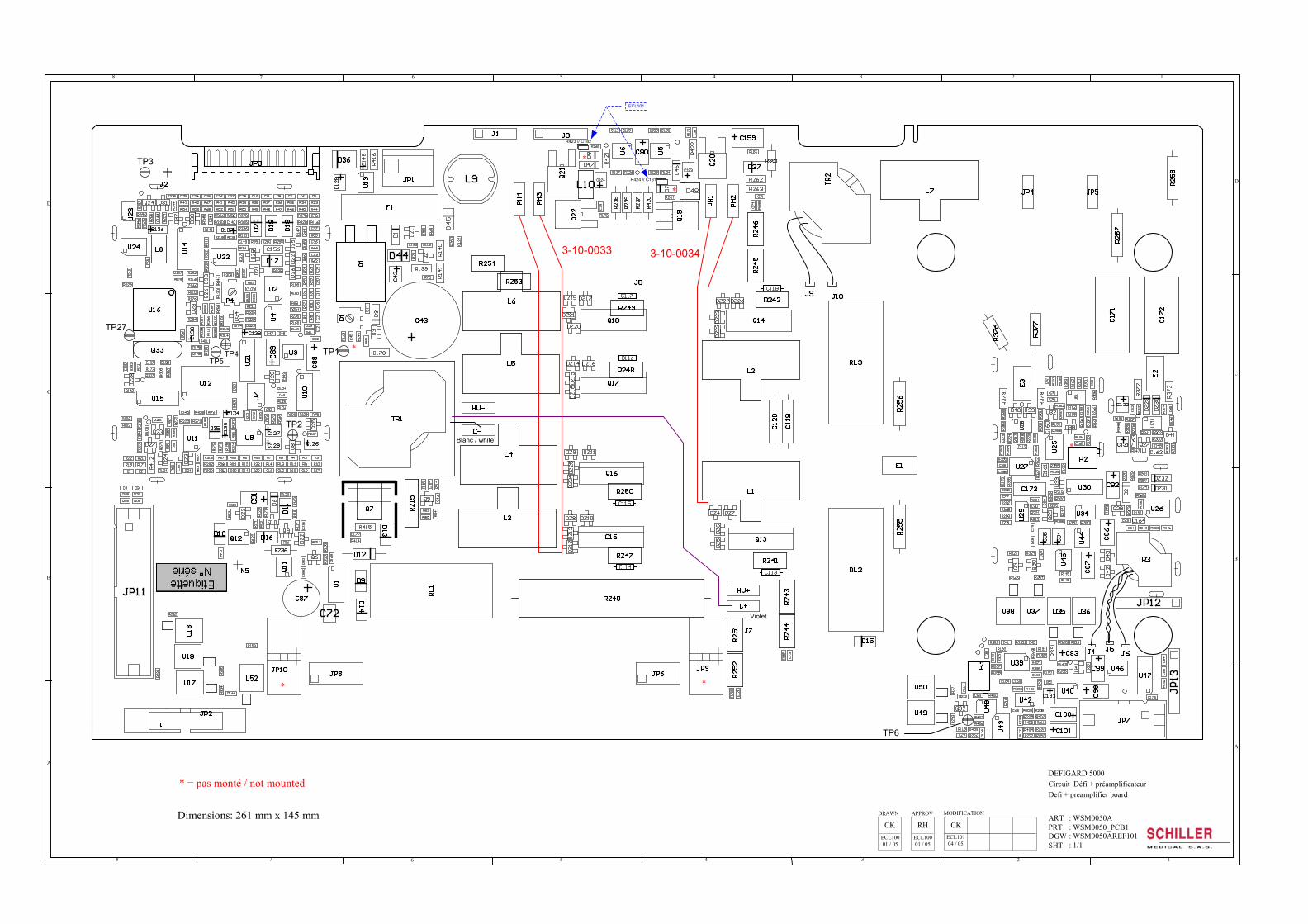
12345678
12345678
D
C
B
A
A
B
C
D
CKDRAWN APPROV MODIFICATION
Defi + preamplifier boardCircuit Défi + préamplificateurDEFIGARD 5000
SHT
ARTPRTDGW
: WSM0050A: WSM0050_PCB1: WSM0050AREF101: 1/1
ECL10001 / 05
RH CKECL10001 / 05
ECL10104 / 05
* = pas monté / not mounted
Dimensions: 261 mm x 145 mm
*
*
*
*
*
*TP3
TP27
TP5TP4
TP2
TP1
TP6
3-10-0033 3-10-0034
Blanc / white
Violet
R423 // C182
R424 // C181
ECL101

Diagrams and layout drawings
0-48-0065 7-5 June 2005
WSM0050_PCB2
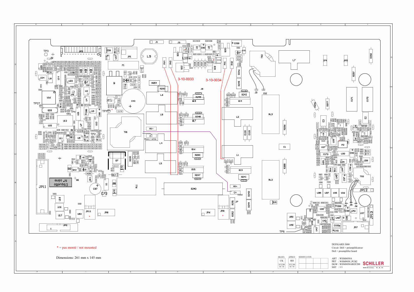
12345678
12345678
D
C
B
A
A
B
C
D
CKDRAWN APPROV MODIFICATION
Defi + preamplifier boardCircuit Défi + préamplificateurDEFIGARD 5000
SHT
ARTPRTDGW
: WSM0050A: WSM0050_PCB2: WSM0050AREF200: 1/1
ECL20004 / 05
RHECL20004 / 05
* = pas monté / not mounted
Dimensions: 261 mm x 145 mm
*
*
*
*
*
*TP3
TP27
TP5TP4
TP2
TP1
TP6
3-10-0033 3-10-0034
Blanc / white
Violet
Diagrams and layout drawings
0-48-0065 7-6 June 2005
7.3. CPU BOARD (part no. 3.2852)
The part number of this board is 3.2652 or WSM0057A.
Diagrams and layout drawings
0-48-0065 7-7 June 2005
D2652BA
Diagrams and layout drawings
0-48-0065 7-8 June 2005
S2652CAD2652CA
Diagrams and layout drawings
0-48-0065 7-9 June 2005
7.4. POWER BOARD (part no. 3.2653)
The part number of this board is 3.2653 or WSM0065A.
Diagrams and layout drawings
0-48-0065 7-10 June 2005
D2653BA
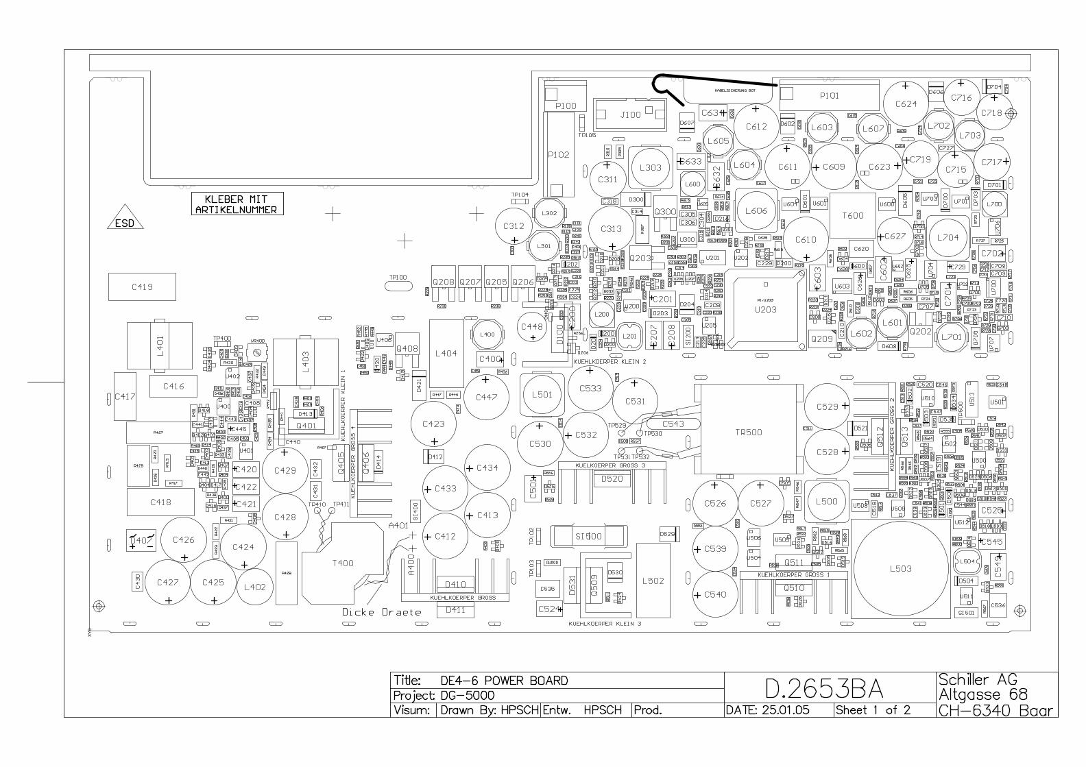
Diagrams and layout drawings
0-48-0065 7-11 June 2005
7.5. UPPER KEYPAD BOARD (part no. WSM0062A)

Diagrams and layout drawings
0-48-0065 7-12 June 2005
WSM0062_PCB1
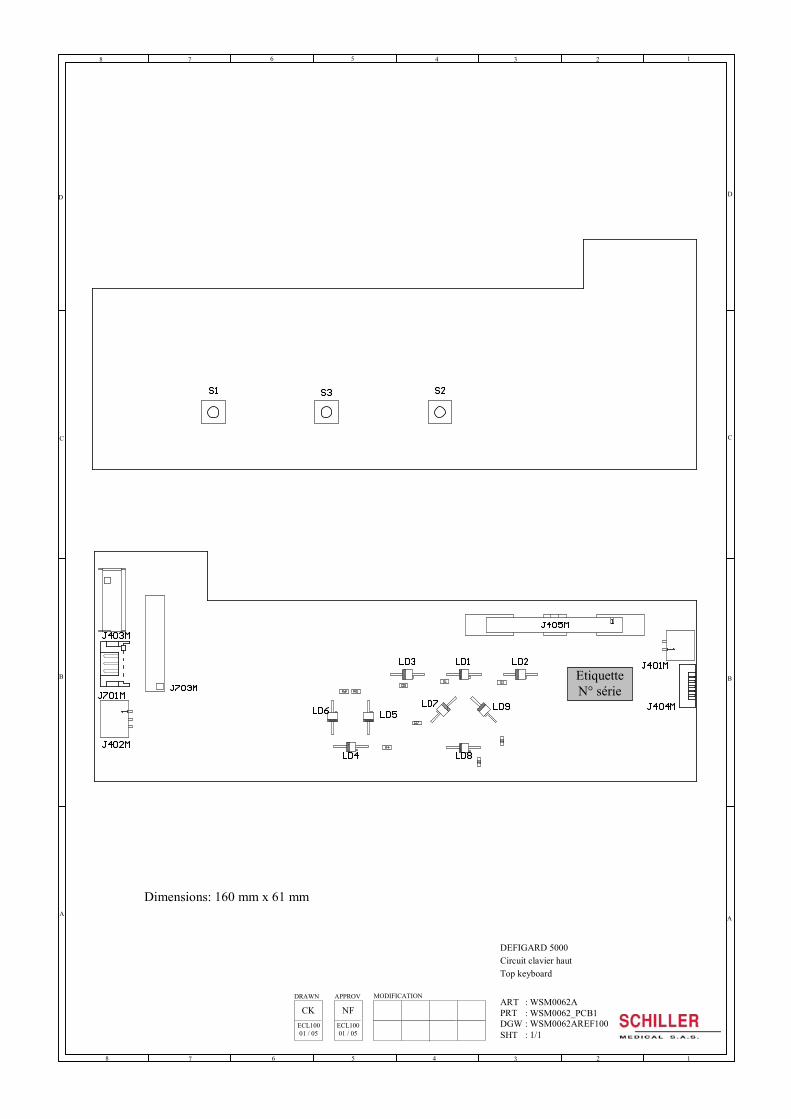
12345678
12345678
D
C
B
AA
B
C
D
CKDRAWN APPROV MODIFICATION
Top keyboardCircuit clavier hautDEFIGARD 5000
SHT
ARTPRTDGW
: WSM0062A: WSM0062_PCB1: WSM0062AREF100: 1/1
ECL10001 / 05
NFECL10001 / 05
Dimensions: 160 mm x 61 mm
EtiquetteN° série
Diagrams and layout drawings
0-48-0065 7-13 June 2005
7.6. KEYPAD + BATTERY BOARD: (part no. WSM0060A)
This circuit is made up of three different snap-off circuits. When the circuits are separated, each has adifferent part number:
- WSM0060B: DG5000 SIDE KEYPAD PCB- WSM0060C: DG5000 BATTERY 1 PCB- WSM0060D: DG5000 BATTERY 2 PCB2

Diagrams and layout drawings
0-48-0065 7-14 June 2005
WSM0060_PCB1
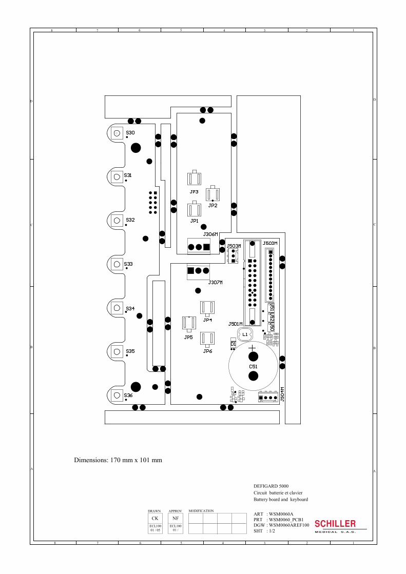
12345678
12345678
D
C
B
AA
B
C
D
CKDRAWN APPROV MODIFICATION
Battery board and keyboardCircuit batterie et clavierDEFIGARD 5000
SHT
ARTPRTDGW
: WSM0060A: WSM0060_PCB1: WSM0060AREF100: 1/2
ECL10001 / 05
NFECL100
01 /
Dimensions: 170 mm x 101 mm
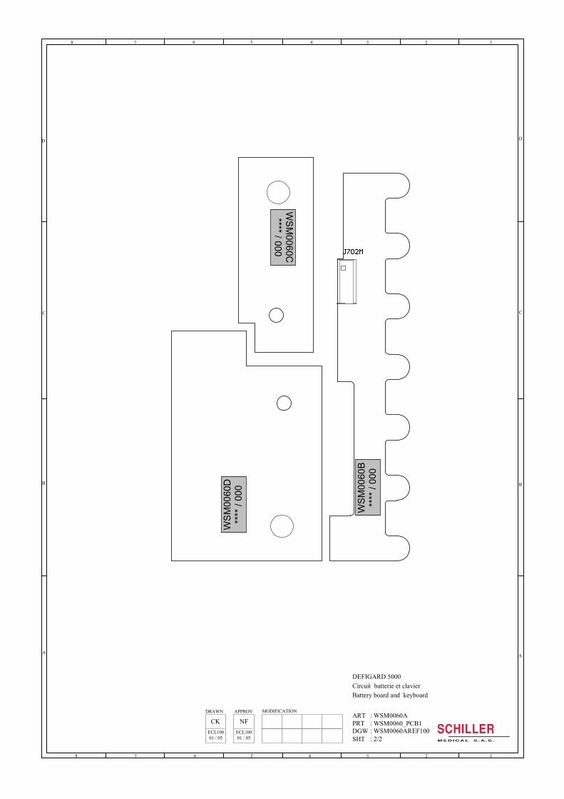
12345678
12345678
D
C
B
AA
B
C
D
CKDRAWN APPROV MODIFICATION
Battery board and keyboardCircuit batterie et clavierDEFIGARD 5000
SHT
ARTPRTDGW
: WSM0060A: WSM0060_PCB1: WSM0060AREF100: 2/2
ECL10001 / 05
NFECL10001 / 05
WSM
0060
D**
** /
000
WSM
0060C**** / 000
WSM
0060
B**
** /
000
Diagrams and layout drawings
0-48-0065 7-15 June 2005
7.7. PACEMAKER BOARD: (part no. WSM0059A)
Diagrams and layout drawings
0-48-0065 7-16 June 2005
WSM0059_PCB0
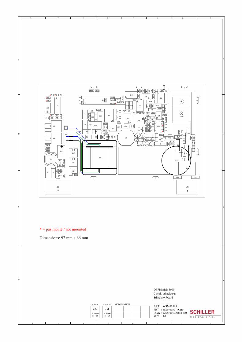
12345678
12345678
D
C
B
AA
B
C
D
CKDRAWN APPROV MODIFICATION
Stimulator boardCircuit stimulateurDEFIGARD 5000
SHT
ARTPRTDGW
: WSM0059A: WSM0059_PCB0: WSM0059AREF000: 1/1
ECL00011 / 04
JMECL00011 / 04
* = pas monté / not mounted
Dimensions: 97 mm x 66 mm
*
R75D10
C33
C34
*
*
R76
D14
*** *
*

Diagrams and layout drawings
0-48-0065 7-17 June 2005
WSM0059_PCB1
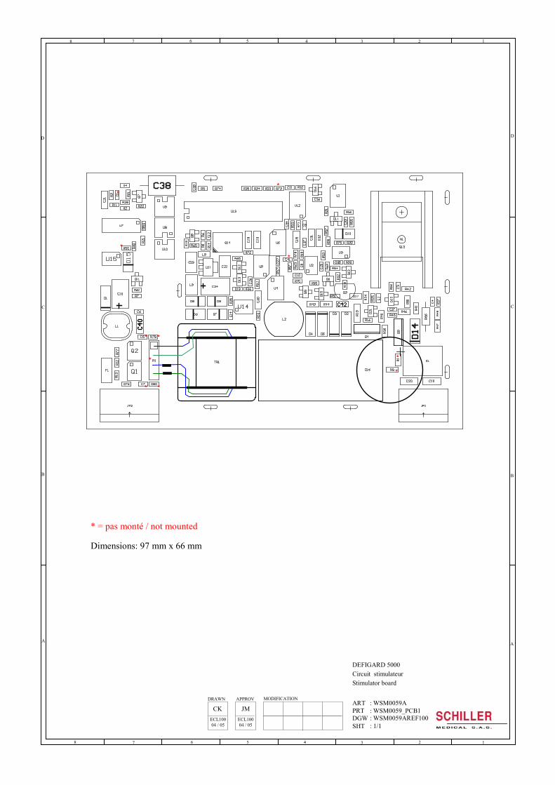
12345678
12345678
D
C
B
AA
B
C
D
CKDRAWN APPROV MODIFICATION
Stimulator boardCircuit stimulateurDEFIGARD 5000
SHT
ARTPRTDGW
: WSM0059A: WSM0059_PCB1: WSM0059AREF100: 1/1
ECL10004 / 05
JMECL10004 / 05
* = pas monté / not mounted
Dimensions: 97 mm x 66 mm
*
*
*
*
*
**
*
*
*
*
Diagrams and layout drawings
0-48-0065 7-18 June 2005
7.8. LCD DISPLAY TFT 800X600 : (part no. 4-30-0001)
Référence AUO : G104SN03
(C) Copyright AU Optronics, Inc. 2004 All Right Reserved. G104SN03 V.0 No Reproduction and Redistribution Allowed.
1.0 Handing Precautions 1) Since front polarizer is easily damaged, pay attention not to scratch it. 2) Be sure to turn off power supply when inserting or disconnection from input connector. 3) Wipe off water drop immediately. Long contact with water may cause discoloration or spots. 4) When the panel surface is soiled, wipe it with absorbent cotton or other soft cloth. 5) Since the panel is made of glass, it may break or crack if dropped or bumped on hard surface. 6) Since CMOS LSI is used in this module, take care of static electricity and insure human earth when
handling. 7) Do not open nor modify the module Assembly. 8) Do not press the reflector sheet at the back of the module to any directions. 9) In case if a module has to be put back into the packing container slot after once it was taken out
from the container, do not press the center of the CCFL Reflector edge. Instead, press at the far ends of the CFL Reflector edge softly. Otherwise the TFT module may be damaged.
10) At the insertion or removal of the Signal Interface Connector, be sure not to rotate nor tilt the interface Connector of the TFT module.
11) After installation of the TFT module into an enclosure, do not twist nor bend the TFT module even momentary. At designing the enclosure, it should be taken into consideration that no bending/twisting forces are applied to the TFT module from outside. Otherwise the TFT module may be damaged.
12) Cold cathode fluorescent lamp in LCD contains a small amount of mercury. Please follow local ordinances or regulations for disposal.
13) Small amount of materials having no flammability grade is used in the LCD module should be supplied by power complied with requirements of Limited Power Source, or be applied exemption.
14) The LCD module is designed so that the CFL in it is supplied by Limited Current Circuit. Do not connect the CFL in Hazardous Voltage Circuit.
(C) Copyright AU Optronics, Inc. 2004 All Right Reserved. G104SN03 V.0 No Reproduction and Redistribution Allowed.
2.0 General Description This specification applies to the 10.4 inch color TFT LCD module G104SN03 V.0. This module is designed for General Display. The screen format is intended to support the SVGA (800(H) x 600(V)) screen and 262k colors (RGB 6-bits data driver). All input signals are LVDS interface compatible. The module does not contain an inverter card for backlight.
Features - SVGA 800(H) x600(V) resolution - 1 CCFL(Cold cathode Fluorescent Lamp) - High contrast ratio, High transmittance ratio - Wide viewing angle - High speed response - Low power consumption - LVDS interface
Applications Information Appliance Industrial Application
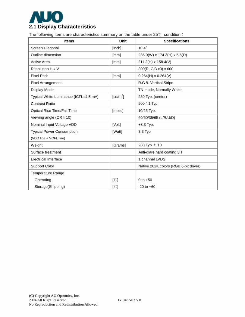
(C) Copyright AU Optronics, Inc. 2004 All Right Reserved. G104SN03 V.0 No Reproduction and Redistribution Allowed.
2.1 Display Characteristics The following items are characteristics summary on the table under 25 condition:
Items Unit Specifications
Screen Diagonal [inch] 10.4”
Outline dimension [mm] 236.0(W) x 174.3(H) x 5.6(D)
Active Area [mm] 211.2(H) x 158.4(V)
Resolution H x V 800(R, G,B x3) x 600
Pixel Pitch [mm] 0.264(H) x 0.264(V)
Pixel Arrangement R.G.B. Vertical Stripe
Display Mode TN mode, Normally White
Typical White Luminance (ICFL=4.5 mA) [cd/m2] 230 Typ. (center)
Contrast Ratio 500:1 Typ.
Optical Rise Time/Fall Time [msec] 10/25 Typ.
Viewing angle (CR≧10) 60/60/35/65 (L/R/U/D)
Nominal Input Voltage VDD [Volt] +3.3 Typ.
Typical Power Consumption
(VDD line + VCFL line)
[Watt] 3.3 Typ
Weight [Grams] 280 Typ ± 10
Surface treatment Anti-glare,hard coating 3H
Electrical Interface 1 channel LVDS
Support Color Native 262K colors (RGB 6-bit driver)
Temperature Range
Operating
Storage(Shipping)
[]
[]
0 to +50
-20 to +60
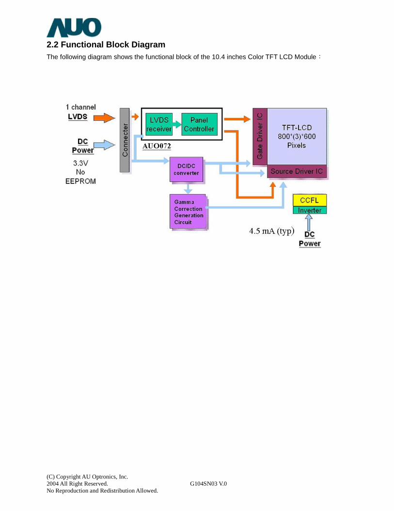
(C) Copyright AU Optronics, Inc. 2004 All Right Reserved. G104SN03 V.0 No Reproduction and Redistribution Allowed.
2.2 Functional Block Diagram The following diagram shows the functional block of the 10.4 inches Color TFT LCD Module:
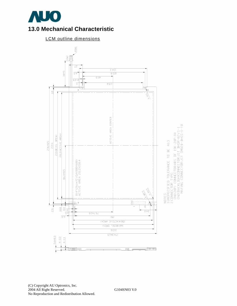
(C) Copyright AU Optronics, Inc. 2004 All Right Reserved. G104SN03 V.0 No Reproduction and Redistribution Allowed.
13.0 Mechanical Characteristic LCM outline dimensions
Diagrams and layout drawings
0-48-0065 7-19 June 2005
7.9. LIGHTING BOARD: (part no. 4-24-0003)
Référence AUO : GH025A
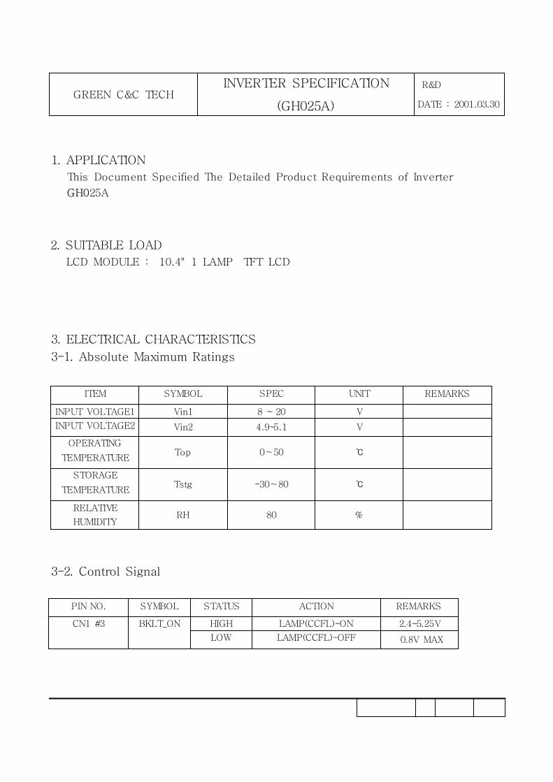
2. SUITABLE LOAD
LCD MODULE : 10.4" 1 LAMP TFT LCD
1. APPLICATION
This Document Specified The Detailed Product Requirements of Inverter
GH025A
3. ELECTRICAL CHARACTERISTICS
3-1. Absolute Maximum Ratings
3-2. Control Signal
PIN NO. SYMBOL STATUS ACTION REMARKS
CN1 #3 BKLT_ON HIGH LAMP(CCFL)-ON 2.4~5.25V
LOW LAMP(CCFL)-OFF 0.8V MAX
ITEM SYMBOL SPEC UNIT REMARKS
INPUT VOLTAGE1 Vin1 8 ~ 20 V
INPUT VOLTAGE2 Vin2 4.9~5.1 V
OPERATING
TEMPERATURETop 0∼50
STORAGE
TEMPERATURETstg -30∼80
RELATIVE
HUMIDITYRH 80 %
GREEN C&C TECHINVERTER SPECIFICATION
(GH025A)
R&D
DATE : 2001.03.30
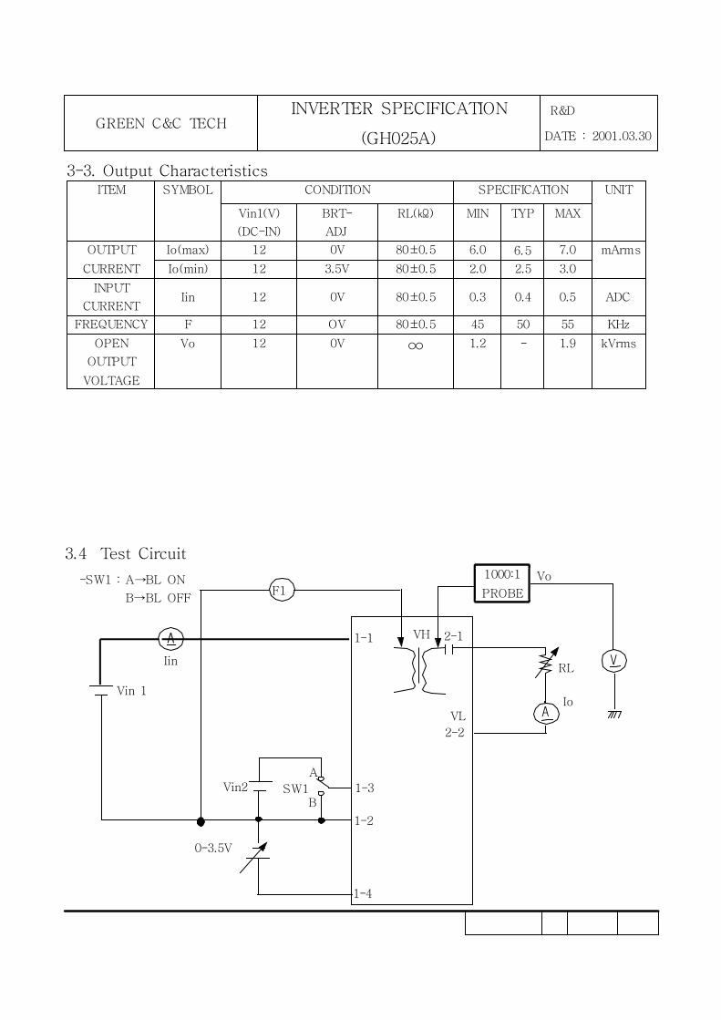
3-3. Output Characteristics
3.4 Test Circuit
A
F1
Iin
Vin 1
-SW1 : A→BL ON
B→BL OFF
1-4
1-1
SW1
0-3.5V
A
B
1-2
VH
AIo
VL
VRL
2-1
2-2
Vo1000:1
PROBE
1-3Vin2
ITEM SYMBOL CONDITION SPECIFICATION UNIT
Vin1(V)
(DC-IN)
BRT-
ADJ
RL() MIN TYP MAX
OUTPUT
CURRENT
Io(max) 12 0V 80±0.5 6.0 6.5 7.0 mArms
Io(min) 12 3.5V 80±0.5 2.0 2.5 3.0
INPUT
CURRENTIin 12 0V 80±0.5 0.3 0.4 0.5 ADC
FREQUENCY F 12 OV 80±0.5 45 50 55 KHz
OPEN
OUTPUT
VOLTAGE
Vo 12 0V ∞ 1.2 - 1.9 kVrms
GREEN C&C TECHINVERTER SPECIFICATION
(GH025A)
R&D
DATE : 2001.03.30
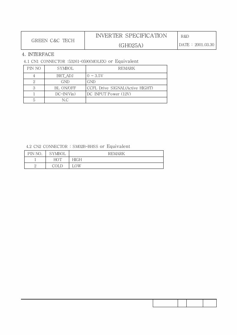
4.2 CN2 CONNECTOR : SM02B-BHSS or Equivalent
PIN NO. SYMBOL REMARK
1 HOT HIGH
2 COLD LOW
4. INTERFACE
4.1 CN1 CONNECTOR :53261-0590(MOLEX) or Equivalent
PIN NO SYMBOL REMARK
4 BRT_ADJ 0 ~ 3.5V
2 GND GND
3 BL ON/OFF CCFL Drive SIGNAL(Active HIGHT)
1 DC-IN(Vin) DC INPUT Power (12V)
5 N.C
GREEN C&C TECHINVERTER SPECIFICATION
(GH025A)
R&D
DATE : 2001.03.30
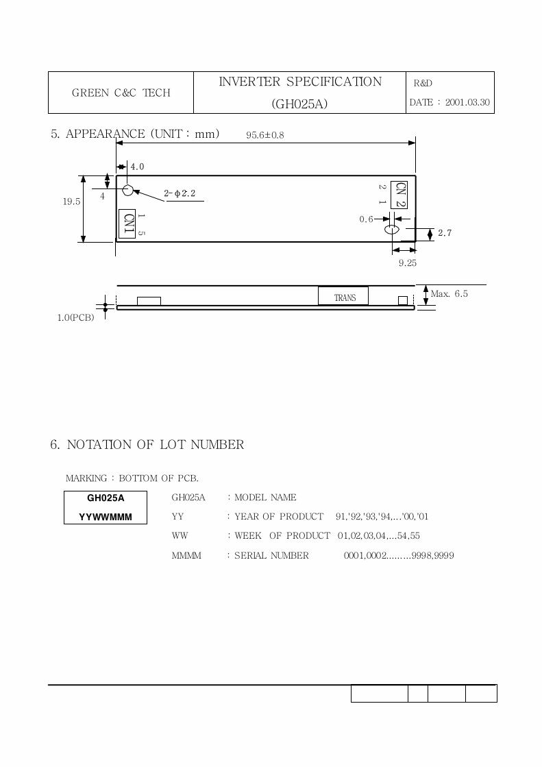
5. APPEARANCE (UNIT : mm)
6. NOTATION OF LOT NUMBER
95.6±0.8
1.0(PCB)
Max. 6.5
4.0
2-φ2.2
2.7
CN1
9.25
19.5
CN2
TRANS
21
15
4
MARKING : BOTTOM OF PCB.
GH025A
YYWWMMM
GH025A : MODEL NAME
YY : YEAR OF PRODUCT 91,'92,'93,'94,...'00,'01
WW : WEEK OF PRODUCT 01,02,03,04,...54,55
MMMM : SERIAL NUMBER 0001,0002...... ...9998,9999
GREEN C&C TECHINVERTER SPECIFICATION
(GH025A)
R&D
DATE : 2001.03.30
0.6
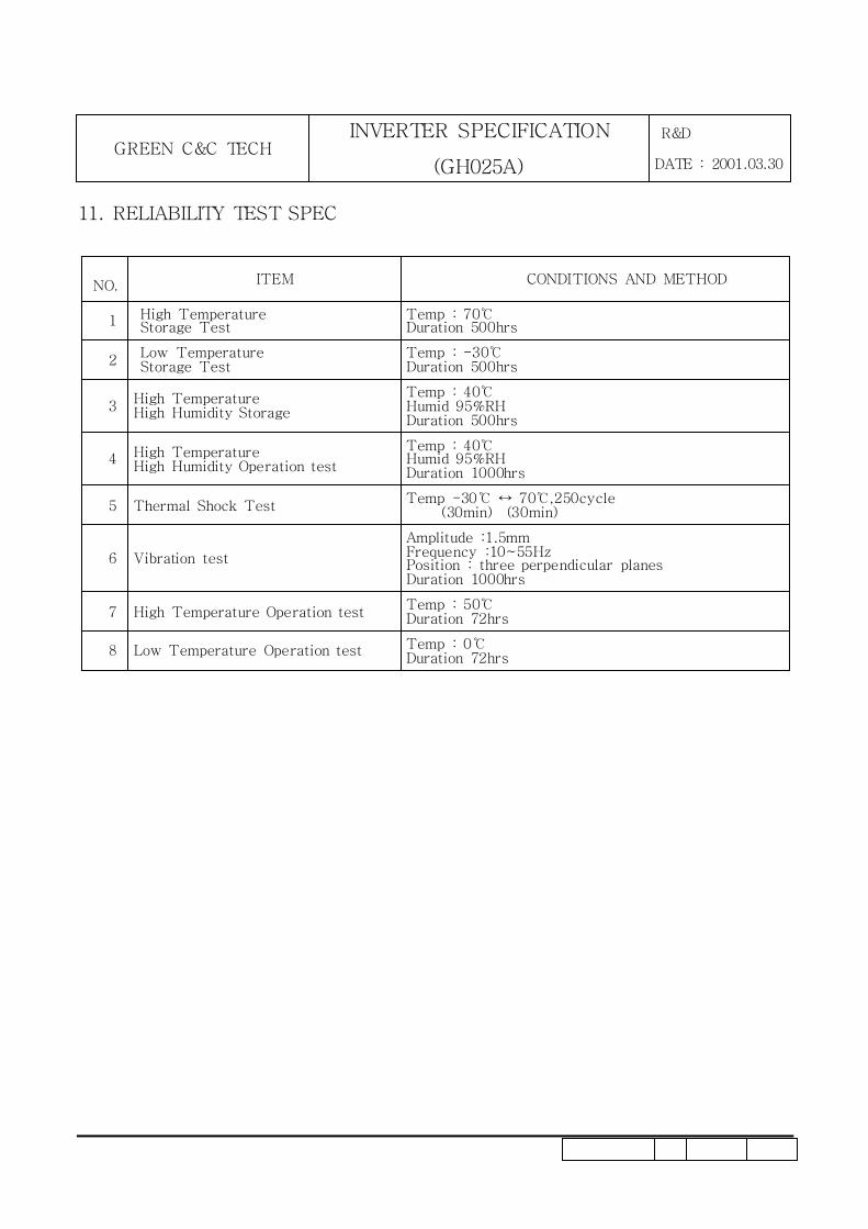
11. RELIABILITY TEST SPEC
NO. ITEM CONDITIONS AND METHOD
1 High TemperatureStorage Test
Temp : 70Duration 500hrs
2Low TemperatureStorage Test
Temp : -30Duration 500hrs
3High TemperatureHigh Humidity Storage
Temp : 40Humid 95%RHDuration 500hrs
4 High TemperatureHigh Humidity Operation test
Temp : 40Humid 95%RHDuration 1000hrs
5 Thermal Shock TestTemp -30 ↔ 70,250cycle
(30min) (30min)
6 Vibration test
Amplitude :1.5mmFrequency :10~55HzPosition : three perpendicular planesDuration 1000hrs
7 High Temperature Operation testTemp : 50Duration 72hrs
8 Low Temperature Operation test Temp : 0Duration 72hrs
GREEN C&C TECHINVERTER SPECIFICATION
(GH025A)
R&D
DATE : 2001.03.30
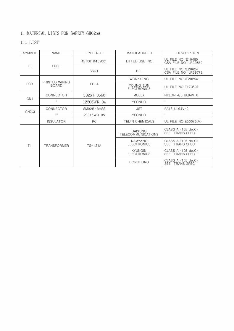
1. MATERIAL LISTS FOR SAFETY GH025A
1.1 LIST
SYMBOL NAME TYPE NO. MANUFACURER DESCRIPTION
FI FUSE
451001&452001 LITTELFUSE INCUL FILE NO :E10480CSA FILE NO :LR29862
SSQ1 BELUL FILE NO :E20624CSA FILE NO :LR39772
PCBPRINTED WIRING
BOARD FR-4
WONKYENG UL FILE NO :E202541
YOUNG EUNELECTRONICS
UL FILE NO:E173507
CN1CONNECTOR 53261-0590 MOLEX NYLON 4/6 UL94V-0
" 12505WR-04 YEONHO "
CN2,3CONNECTOR SM02B-BHSS JST PA46 UL94V-0
"'' 20015WR-05 YEONHO "
INSULATOR PC TEIJIN CHEMICALS UL FILE NO:E50075(M)
T1 TRANSFORMER TS-121A
DAISUNGTELECOMMUNICATIONS
CLASS A (105 de.C)SEE TRANS SPEC
NAMYANGELECTRONICS
CLASS A (105 de.C)SEE TRANS SPEC
KYUNGINELECTRONICS
CLASS A (105 de.C)SEE TRANS SPEC
DONGHUNGCLASS A (105 de.C)SEE TRANS SPEC