Embed Size (px)
Citation preview
DEPARTMENT OF ELECTRICAL ENGINEERING AND COMPUTER SCIENCE MASSACHUSETTS INSTITUTE OF TECHNOLOGY
CAMBRIDGE, MASSACHUSETTS 02139
6.101 Introductory Analog Electronics Laboratory Laboratory No. 2
READING ASSIGNMENT You should have read the diode reading assignments in the course outline before doing this lab. For this laboratory, you will need to refer to the instruction manual for the Tektronix 577-177 or 575 Curve Tracers [manuals may be signed out at the 38-501 stockroom window]. At a minimum, you should refer to the section of the manuals entitled Applications that describes how to set up the curve tracer to make measurements on specific devices such as diodes, bipolar transistors, etc. Since the 577-177 is a severely ergonometrically-challenged design, it is strongly suggested that you use the model 575. Simplified instructions for the 575 curve tracers are chained to the instruments in the lab and are also available at the stockroom window. DANGER: HIGH VOLTAGE is available on the collector terminals of any curve tracer depending on the setting of the collector voltage switch and the variable collector voltage pot position. Be sure to turn the transistor selector switch to the center “off” position before inserting or removing transistors, and to keep your hands free while applying voltage. [This voltage is pulsed and is current limited, but may still “surprise” you if you touch the collector terminals!] SPECIAL CURVE TRACER SETUP: One of the curve tracers has been modified to allow the curves to be displayed on the new Tektronix sampling scopes. While the curves are not as clean as those displayed on an analog display, the new scopes do allow you to print your displays to a floppy disc. I suggest that you use .TIF file types for these curves. Instructions for using this hybrid curve tracer are posted on the equipment. This will save lots of sketching of device curves. OBJECTIVE Diodes! Zener diodes! Bipolar Transistors! OpAmps! Power Supplies! These are some of the fundamental devices and circuits in analog electronics. You will learn more about our test equipment, and you’ll study some of the properties of the devices above. You will also build three [count ‘em!] [3] different linear [non-switching] power supplies and compare them. You will learn how to display the input-output characteristics of some of these devices on our antique [but still very useful] curve tracers. Experiment 1: Diode Fundamentals: Building a Simple Log Amplifier.
Lab. No. 2 1 9/1103
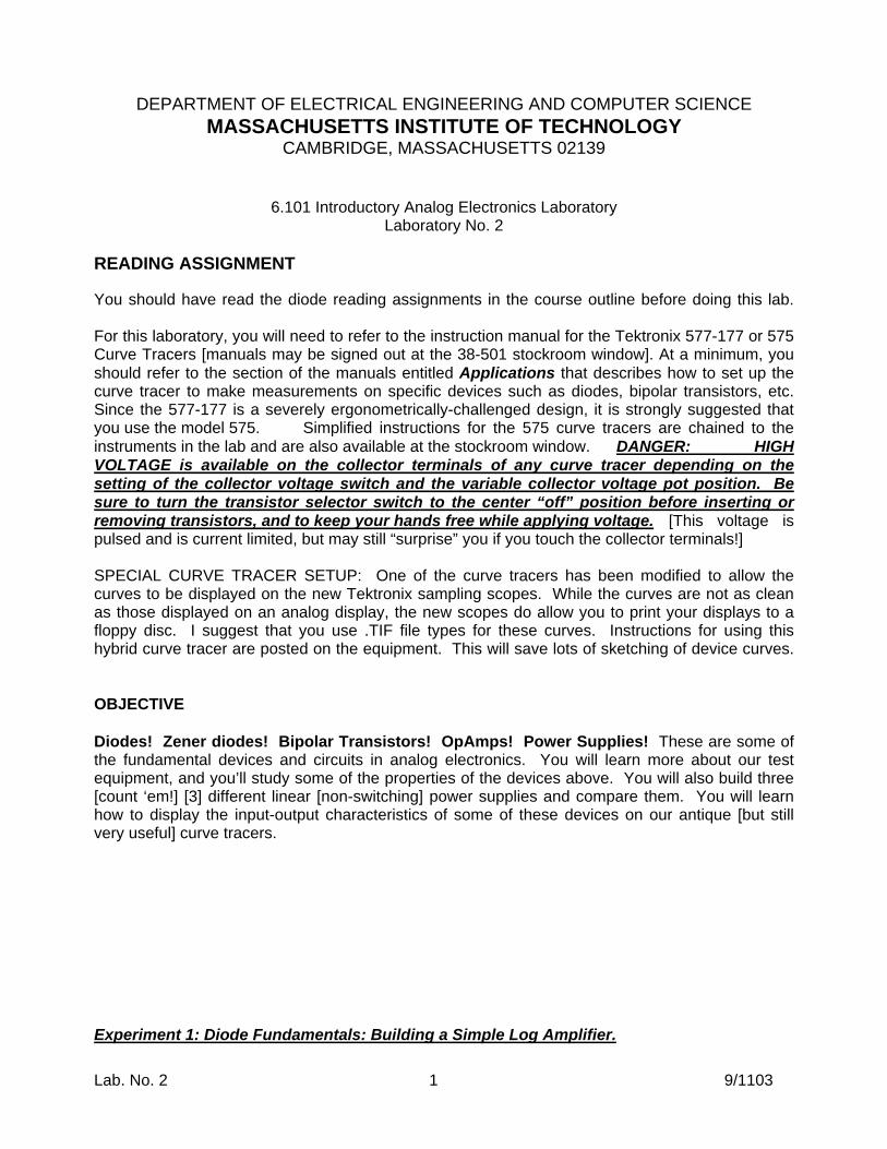
In this experiment, you will learn more about the diode by studying a simple log amplifier.
Simple Logarithmic Amplifier
[You need to know that the voltage gain of this amplifier is Ω
−=−=k
RVV
A diode
in
outV 0.1
; you also need to
know that the inverting input, pin 2, is a virtual ground, in this case, for both AC and DC signals.] [We suggest that you express Rdiode in more useful terms!] 1. Build the logarithmic amplifier shown in figure 1. Q 1.1 What is the ideal input/output relationship VOUT versus VIN for this amplifier when the diode is biased with forward current? Q1.2 For what range of input voltages is there a logarithmic VOUT versus VIN relationship? 2. When the diode is forward biased, the diode voltage/current relationship is given by:
ID IS e
qVDkT
ISe
qVDkT
= − ≈
⎡
⎣⎢
⎤
⎦⎥
⎡
⎣⎢
⎤
⎦⎥
( )1
where kT/q is the thermal voltage [≈ 26 mV at room temperature] and IS is the diode reverse saturation current which depends on the particular device, temperature, etc. Q 1.3 When the diode forward current is increased by a factor of 10, how much does the diode voltage change?
-
+
+15
LF356
2
34
76
vin
vout+
_ -15
1.0kΩ
1N914
Figure 1: Circuit for Experiment 1
3. Plot the amplifier input/output relationship for 10 mV < VIN < 1000 mV. Use the DC offset adjustment control on your Function Generator to provide the DC voltage source. Make sure that the AC signal from the generator is turned off. To do this, press and hold the button labeled OFFSET for two seconds or until you hear a click. This will produce a pure DC output without any AC riding on top of it. Put one of your scope probes at the output of the amplifier to observe the output and to make sure that the only signal present is a DC signal. You should use your DMM to read first the input voltage [set to a convenient value], and then move the DMM to the output terminal to read the output DC voltage. Measure for several points per decade of input voltage, and use semi-log axes; this should result in a linear plot on semi-log axes.
Lab. No. 2 2 9/1103
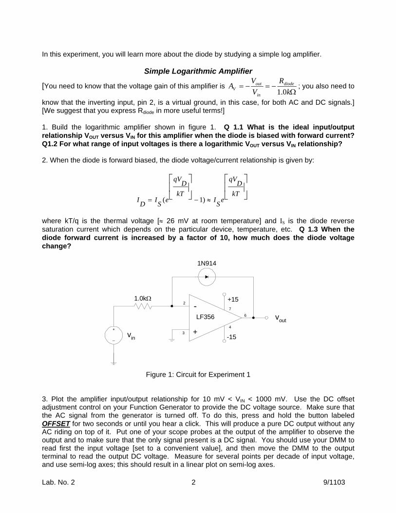
4. Q 1.4 Find the diode coefficient IS from your data. You will need to know that the current entering pin 2 of the operational amplifier is negligible compared to the current through the diode, at least at the higher DC input voltages. If you find that the logarithmic relationship between input and output disappears at low DC input voltages, it may be due to the fact that the pin 2 input current is the same order of magnitude as the current through the diode at low input voltages. This can still happen even though the LM356 has a JFET input stage, and thus very very low input bias current. 5. Q 1.5 Measure an approximate temperature coefficient for the diode voltage, in mV/oC. [Hint: this can be done with the diode operating in your circuit; we want you to make a very rough estimate of the diode temperature coefficient. One possible method to change the temperature of the diode is to hold the diode between your thumb and forefinger with your fingers. Hold the diode until the output voltage stops changing.] Q 1.6 Comment on the practicality of using this amplifier in a piece of equipment where the temperature may vary widely [for instance, in a piece of commercial electronics where the ambient temperature may vary from 40oF to 150oF]. 6. Replace the 1N914 in your circuit with another 1N914 from your kit or from the drawers in the lab. On the same set of axes, plot the VOUT/VIN relationship. Q 1.6 Observe if there are any differences between the two curves, and explain why.
+
v in
-
1N4001
1.0k Ω
+
v out
-
Figure 2: Circuit for Experiment 2.
Experiment 2: Rectifier diodes. 1. Use the curve tracer to measure the characteristics of a 1N4001 rectifier diode from your lab kit. [Solder smaller diameter wires to the leads of your diode to get it to fit into the socket on the curve tracer; otherwise you will damage the curve tracer socket. Or, you can attach the diode to the curve tracer using the binding posts.] Refer to the section entitled SIGNAL AND RECTIFYING DIODES on page 33 of the 577-177 manual, or use the setup for Diode Forward Characteristic on page 4 of the manual attached to the 575 Curve Tracer [attached]. [The forward characteristics of a zener diode and an ordinary rectifier or signal diode are all measured in the same manner.] In your lab notebook [or on a separate piece of linear graph paper which you can insert in your lab notebook] plot the diode v - i characteristic for currents up to 20 mA. Repeat this plot on semi-log paper, using the log scale for the y-axis [current]. 2. Construct the circuit of Figure 2. Apply a 100 Hz, 6 V peak-peak signal from the signal generator to the input, vin . Measure the peak value of the output voltage vout and the fraction of
Lab. No. 2 3 9/1103
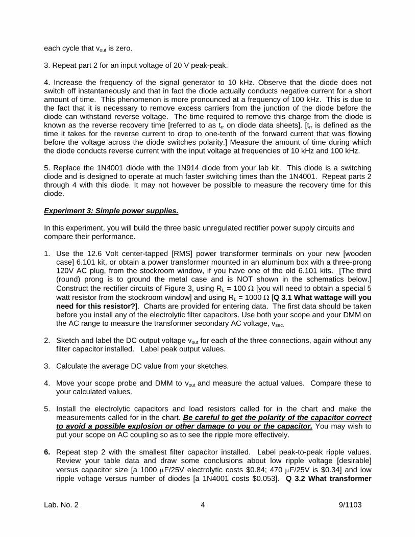
each cycle that vout is zero. 3. Repeat part 2 for an input voltage of 20 V peak-peak. 4. Increase the frequency of the signal generator to 10 kHz. Observe that the diode does not switch off instantaneously and that in fact the diode actually conducts negative current for a short amount of time. This phenomenon is more pronounced at a frequency of 100 kHz. This is due to the fact that it is necessary to remove excess carriers from the junction of the diode before the diode can withstand reverse voltage. The time required to remove this charge from the diode is known as the reverse recovery time [referred to as trr on diode data sheets]. [trr is defined as the time it takes for the reverse current to drop to one-tenth of the forward current that was flowing before the voltage across the diode switches polarity.] Measure the amount of time during which the diode conducts reverse current with the input voltage at frequencies of 10 kHz and 100 kHz. 5. Replace the 1N4001 diode with the 1N914 diode from your lab kit. This diode is a switching diode and is designed to operate at much faster switching times than the 1N4001. Repeat parts 2 through 4 with this diode. It may not however be possible to measure the recovery time for this diode. Experiment 3: Simple power supplies. In this experiment, you will build the three basic unregulated rectifier power supply circuits and compare their performance. 1. Use the 12.6 Volt center-tapped [RMS] power transformer terminals on your new [wooden
case] 6.101 kit, or obtain a power transformer mounted in an aluminum box with a three-prong 120V AC plug, from the stockroom window, if you have one of the old 6.101 kits. [The third (round) prong is to ground the metal case and is NOT shown in the schematics below.] Construct the rectifier circuits of Figure 3, using RL = 100 Ω [you will need to obtain a special 5 watt resistor from the stockroom window] and using RL = 1000 Ω [Q 3.1 What wattage will you need for this resistor?]. Charts are provided for entering data. The first data should be taken before you install any of the electrolytic filter capacitors. Use both your scope and your DMM on the AC range to measure the transformer secondary AC voltage, vsec.
2. Sketch and label the DC output voltage vout for each of the three connections, again without any
filter capacitor installed. Label peak output values. 3. Calculate the average DC value from your sketches. 4. Move your scope probe and DMM to vout and measure the actual values. Compare these to
your calculated values. 5. Install the electrolytic capacitors and load resistors called for in the chart and make the
measurements called for in the chart. Be careful to get the polarity of the capacitor correct to avoid a possible explosion or other damage to you or the capacitor. You may wish to put your scope on AC coupling so as to see the ripple more effectively.
6. Repeat step 2 with the smallest filter capacitor installed. Label peak-to-peak ripple values. Review your table data and draw some conclusions about low ripple voltage [desirable] versus capacitor size [a 1000 µF/25V electrolytic costs $0.84; 470 µF/25V is $0.34] and low ripple voltage versus number of diodes [a 1N4001 costs $0.053]. Q 3.2 What transformer
Lab. No. 2 4 9/1103
secondary voltage would be required to make the output of the full-wave rectifier circuit equal to the output of the bridge or half-wave rectifier circuits?
C F R L
1N4001
3a) Half-wave rectifier circuit diagram
120 V 60 Hz
+
v OUT
-
Pri Sec
12.6 VCT RMS
C F R L
3b) Full-wave rectifier circuit diagram
1N4001
+
v OUT
-
Pri Sec
12.6 VCT RMS
1N4001
120 V 60 Hz
R L
3c) Bridge rectifier circuit diagram
CF
+
v OUT
-
Pri Sec
12.6 VCT RMS120 V 60 Hz
4x 1N4001
+
+
+
Figure 3: Circuits for Experiment 3
Lab. No. 2 5 9/1103

Table for Rectifier Circuits Data; 100 Ω Load
Circuit Capacitor size
Vsecondary [p-p]
Vsecondaryrms [DMM]
Vout DC [DMM]
Vripple [p-p]
Ripple frequency
none
470 µF
1000 µF
Half-wave
1470 µF
none
470 µF
1000 µF
Full-wave
1470 µF
none
470 µF
1000 µF
Bridge
1470 µF
Table for Rectifier Circuits Data; 1000 Ω Load
Circuit Capacitor size
Vsecondary [p-p]
Vsecondaryrms [DMM]
Vout DC [DMM]
Vripple [p-p]
Ripple frequency
none
470 µF
1000 µF
Half-wave
1470 µF
none
470 µF
1000 µF
Full-wave
1470 µF
none
470 µF
1000 µF
Bridge
1470 µF
Lab. No. 2 6 9/1103
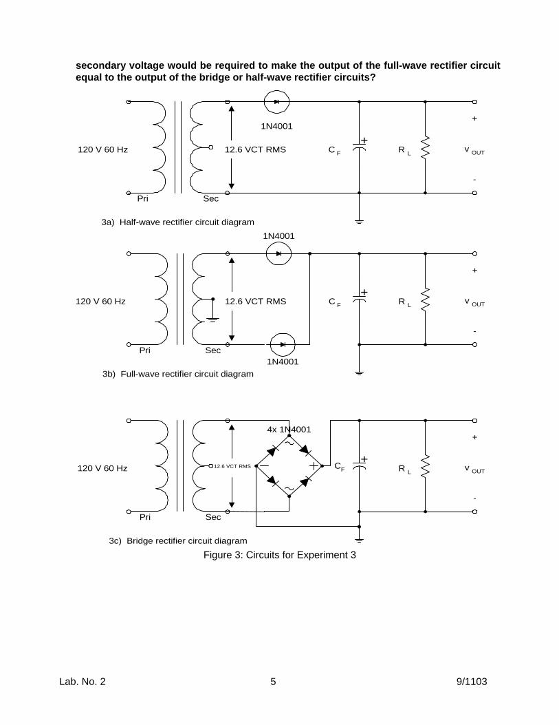
Experiment 4: Zener diodes. As you will see, Zener diodes have a constant-voltage component of their reverse V - I characteristic which makes them useful as voltage regulators in simple power supplies and as voltage references in more complex power supplies and other applications.
+15 V
1N754 R
1.2 kΩ
Figure 4: Circuit for Experiment 4.
1. Use the curve tracer to measure the characteristics of the 1N754 Zener diode from your lab kit. Refer to the section entitled ZENER DIODES on page 35 of the 577-177 manual, or page 5 of the 575 manual. [Your zener point will be a different voltage from that listed in the manual.] Plot the diode V - I characteristic for currents up to 20 mA in both forward and reverse directions. 2. Construct the circuit shown in Figure 4. Measure the voltage across resistor R for R = 10kΩ, R = 1.0 kΩ, and R = 100 Ω. 3. Calculate the value of R in Figure 4 for which the Zener diode will no longer provide voltage regulation. Verify your calculation experimentally. [Q 4.1 Explain why the Zener stops regulating for certain values of R. Hint: think “voltage divider” or “current divider”.] Experiment 5: Bipolar transistors. In this experiment, you will look at the basic characteristics of bipolar transistors. In later experiments you will look at some practical applications of these devices. For transistor number 1 only, sketch or draw or print the characteristic curves from the curve tracer display onto linear graph paper. 0.25 inch grid paper will be plenty good enough. You will need four [4] 2N3904 NPN transistors from your lab kit or from the drawers in the lab. 1. Use the curve tracer to measure the characteristics of a 2N3904 NPN transistor from your lab kit. Label this transistor as number 1 so that you can distinguish it from the remaining 2N3904 transistors in your lab kit. Refer to the section entitled BIPOLAR TRANSISTORS on page 19 of the 577-177 manual, or to pages 9ff in the 575 manual [page 9 attached]. Specifically, set the curve tracer to measure the transistor collector current IC as a function of collector-emitter voltage VCE for 10 steps of base current at 5 µA/step. Set the MAX PEAK POWER WATTS control to 0.6 watts [model 577-177 only].
Lab. No. 2 7 9/1103
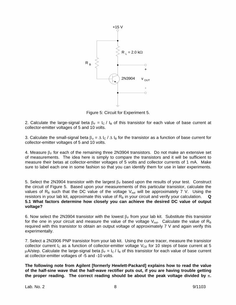
+
v OUT
-
R B
R L = 2.0 kΩ
+15 V
2N3904
Figure 5: Circuit for Experiment 5.
2. Calculate the large-signal beta βF = IC / IB of this transistor for each value of base current at collector-emitter voltages of 5 and 10 volts. 3. Calculate the small-signal beta βo = ∆ IC / ∆ IB for the transistor as a function of base current for collector-emitter voltages of 5 and 10 volts. 4. Measure βF for each of the remaining three 2N3904 transistors. Do not make an extensive set of measurements. The idea here is simply to compare the transistors and it will be sufficient to measure their betas at collector-emitter voltages of 5 volts and collector currents of 1 mA. Make sure to label each one in some fashion so that you can identify them for use in later experiments. 5. Select the 2N3904 transistor with the largest βF based upon the results of your test. Construct the circuit of Figure 5. Based upon your measurements of this particular transistor, calculate the values of RB such that the DC value of the voltage Vout will be approximately 7 V. Using the resistors in your lab kit, approximate this value of RB in your circuit and verify your calculation. Q 5.1 What factors determine how closely you can achieve the desired DC value of output voltage? 6. Now select the 2N3904 transistor with the lowest βF from your lab kit. Substitute this transistor for the one in your circuit and measure the value of the voltage Vout. Calculate the value of RB required with this transistor to obtain an output voltage of approximately 7 V and again verify this experimentally. 7. Select a 2N3906 PNP transistor from your lab kit. Using the curve tracer, measure the transistor collector current IC as a function of collector-emitter voltage VCE for 10 steps of base current at 5 µA/step. Calculate the large-signal beta βF = IC / IB of this transistor for each value of base current at collector-emitter voltages of -5 and -10 volts. The following note from Agilent [formerly Hewlett-Packard] explains how to read the value of the half-sine wave that the half-wave rectifier puts out, if you are having trouble getting the proper reading. The correct reading should be about the peak voltage divided by π.
Lab. No. 2 8 9/1103

”The 34401A does not auto-range very well when measuring AC signals in DC mode. Since the AC does integrate down it chooses the wrong range, too small and then the input is overdriven. You have to manually select a range where the AC signal will not clip. For 17V peak you will need the 100V range. Then it should work correctly. The integration time can be set from using the MEAS command, from the menu or from the keys with the blue Digits and the blue numbers 4,5,6. To use them press the shift key (also blue) then the key, for example if you want to change to 4.5 digits press shift then the down arrow key (it has the blue 4 above it). The integration time will not effect this measurement unless it is less than a full period of the signal you are measuring. Since this is a 60Hz signal anything with an NPLC of 1 or more will work. Yes we could have made the auto-range algorithm work on this kind of signal but it would have made it much slower and most users want it to work fast on DC. Best regards, Hal Wright Agilent Technologies”
Lab. No. 2 9 9/1103
DEPARTMENT OF ELECTRICAL ENGINEERING AND COMPUTER SCIENCE MASSACHUSETTS INSTITUTE OF TECHNOLOGY
CAMBRIDGE, MASSACHUSETTS 02139
HOW TO ADJUST THE STEP-ZERO ON THE 575 CURVE TRACER
1. First, make sure that the Vertical and Horizontal displays are zeroed: Hold the calibration switch for each one at zero, and position the dot so it lies in the lower left corner of thegraticule for NPN devices, and in the upper right corner of the graticule for PNP devices.This is best done with no transistor under test [TUT] connected, and with the PEAK VOLTS pot turned fully CCW.
2. Next, insert, for this example, an NPN device into the test socket, and set the Vertical gainfor 0.5mA/DIV, and the Horizontal gain for 2V/DIV. Set the base current for 0.005mA/STEP, set the switch to “Repetitive” and turn the STEP ZERO control fully CW.
3. Adjust the STEPS/FAMILY pot fully CCW, to 4 STEPS/FAMILY. You will actually see FIVEsteps, the IB = 0 step, and then the 4 steps corresponding to IB = .005 mA, .010 mA, .015 mA, and .020 mA.
4. Once you have verified that there are five steps, now increase the base current stepselector to 0.01 mA/STEP. The upper steps will disappear but it will be easier to view the0th step.
5. Push up the ZERO CURRENT switch and note where the 0th step falls. Release the switch and adjust the STEP ZERO pot CCW until the 0th step just moves down to the bottom line on the graticule [IC=0, IB=0]. DO NOT TURN THE KNOB ANY FURTHER!. If you continueto turn the knob, the 0th step trace will not go any lower, but the 1st, 2nd, 3rd, 4th traces etc will move downward and thus screw up the calibration. You may want to alternate pushing upand releasing the ZERO CURRENT switch while you turn the step zero knob.
6. You should not have to repeat this calibration unless you use a PNP transistor or someone else comes along and decides to do this adjustment improperly!
7. When you view the curves for JFET’s on this curve tracer, be sure to connect the 1000 ohmresistor across the base emitter terminals to convert base mA to gate volts. Then, when you do the calibration procedure above, just be sure to set the switch to ZERO VOLTSduring the calibration procedure.
Lab. No. 2 10 9/1103

Lab. No. 2 11 9/1103

Reverse Recovery Time
Lab. No. 2 12 9/1103
For more information on reverse recovery time, please look at the article written by Anton Kruger at:
http://www.chipcenter.com/eexpert/akruger/akruger004.html