Embed Size (px)
Citation preview

A Thesis on
Development of Low Power Wireless Sensor
Network Node - an SOC Approach
Submitted for partial fulfillment of award of
Degree of
Doctor of Philosophy from
School of Electronics
By Kshitij Shinghal
Under the Supervision of
Dr. Arti Noor & Dr. R.P. Agarwal
SHOBHIT UNIVERSITY
Meerut, INDIA
2013

Dedicated to Memories of my Sister
Aparajita

i
Candidate Declaration
I, hereby, declare that the work presented in this thesis entitled
“Development of Low Power Wireless Sensor Network Node – an SOC
Approach” in fulfillment of the requirements for the award of Degree of
Doctor of Philosophy, submitted in the School of Electronics at Shobhit
University, Modipuram, Meerut is an authentic record of my own research
work under the supervision of Dr. Arti Noor & Dr. R. P. Agarwal.
I also declare that the work embodied in the present thesis
(i) is my original work/extension of the existing work and has not been
copied from any Journal/thesis/book, and
(ii) has not been submitted by me for any other Degree/Diploma.
(Kshitij Shinghal)

ii
Certificate of the Supervisor (s)
This is to certify that the thesis entitled “Development of Low Power
Wireless Sensor Network Node – an SOC Approach” submitted by Kshitij
Shinghal for the award of Degree of Doctor Philosophy in the School of
Electronics of Shobhit University, Meerut is a record of authentic work carried
out by him under our supervision.
The matter embodied in this thesis is the original work of the candidate and
has not been submitted for the award of any other degree or diploma.
It is further certified that he has worked with me for the required period in the
School of Electronics, Shobhit University, Modipuram, Meerut.
(Dr. Arti Noor) (Dr. R.P. Agarwal)

iii
Acknowledgement
First and foremost I would like to thank Almighty God for giving me life,
health and ability to study.
No volume of words is enough to express my gratitude towards my guide Dr.
Arti Noor, for her invaluable guidance and support. Inspite of having so much
busy schedule; she has given me the time for solving my problems during the
work. There was once a time I almost lost all hopes and was demotivated. She
supported and helped me a lot to overcome that phase. I feel privileged and
proud to have such a genial person as my supervisor.
I would also like to give a special thanks to my supervisors Dr. R. P. Agarwal
and Dr. Neelam Srivastava for their valuable guidance and support. I would
also like to pay special regards and thanks to Prof. S. K. Srivastava,
Prof. R. Yadav and Prof. O. P. Singhal for the motivation and inspiration that
triggered me for the thesis work.
I wish to thank all my friends. Special thanks to Mr. Amit Saxena and Nishant
Saxena for their valuable suggestions to improve the quality of this work.
This work would not have been possible without the support from my family.
I am highly thankful to my mother Ms. Suneeta Shinghal for encouraging and
supporting me. I could not have succeeded without her unconditional love,
support, and prayers.

iv
And of course, special thanks to my wife Ms. Deepti Shinghal, my children
Shashwat Shinghal and Arjun Shinghal who has put up with me throughout
all this, caring and supporting me, and most of all believing in me.
Kshitij Shinghal

v
Abstract
Wireless Sensor Networks (WSN) is rapidly getting more and more important
in today’s society. Since the WSN nodes need to be easily deployed they
require being battery powered. Power consumption is one of the most crucial
design issues in WSN nodes. Increasing the WSN nodes lifetime depends on
the efficient management of available energy. In this thesis, a low power WSN
node with new approach for energy management is introduced. In the
proposed WSN node, to achieve energy conservation, the amount of data
transmitted was reduced through data compression by lowering the transceiver
duty cycle and frequency of data transmissions using an event-driven
transmission strategy. In an event-driven transmission strategy data is
transmitted only when the data sensed by the sensor is above a particular
threshold value, which is identified as event occurs. Power reduction strategies
for the different components of WSN node were also applied like gating off
power supply of the components. It is gated on only when the components are
used.
The hardware of WSN node has been designed and implemented in this thesis.
Tests of the WSN node have been performed and the results have shown that
the designed node works very well and fulfills all of the requirements.
Furthermore the power consumption is reduced significantly prolonging the
life of WSN node.

vi
Further an attempt was made to design and simulate a customized processing
unit – an event processor for optimizing the power consumption of the WSN
node. Designing such a processing unit is a highly challenging task that
requires new approaches in many different aspects of the whole system design
and even the design methodology itself. The results were very good and all
components of customized processing unit – an event processor were working
as planned. This thesis has produced a very good platform to use as a base for
further development of a low power WSN node. Wireless Sensor Network
technology offers significant potential in numerous applications. However,
there are significant amount of technical challenges and design issues those
needs to be addressed.

vii
Table of Contents
Candidate Declaration i
Certificate of the Supervisor (s) ii
Acknowledgement iii
Abstract v
Table of Contents vii
List of Figures xiv
List of Tables xviii
List of Abbreviations xx
1 Introduction 1
1.1 Wireless Sensor Network (WSN) Introduction 2
1.2 Brief Historical Survey of Sensor Networks 7
1.3 Applications of Wireless Sensor Network 9
1.4 Agriculture and Environmental Monitoring 11
1.4.1 Precision Agriculture Application 11
1.5 Technical Challenges 12
1.6 Performance Metrics of Wireless Sensor
Network
12
1.7 Summary of the Chapter 14
2 Survey and Research Methodology 15
2.1 Introduction 16
2.2 Various types of WSN nodes 18
2.2.1 Power Consumption 19

viii
2.2.2 Node Unit Costs 20
2.2.3 Environment 20
2.2.4 Energy Consumption 21
2.3 Hardware of existing WSN node 23
2.4 Issues with wireless sensor network nodes 25
2.4.1 Reliability 25
2.4.2 Importance of Energy Management 25
2.4.3 Methods of Energy Management 26
2.4.3.1 Using data reduction
techniques
26
2.4.3.2 Nodes switch between
active (on) and sleeping
(off) mode
27
2.4.3.3 Nodes are independent 27
2.4.3.4 Event based
communication
29
2.4.3.5 By reducing the coverage
area
30
2.4.3.6 Scavenging Energy 30
2.5 Literature survey of WSN for agriculture
applications
31
2.6 Objectives 36
2.7 Research Approach and Strategy 38
2.8 Thesis outline 40
2.9 Summary of the Chapter 43

ix
3 Design and Implementation of WSN Node 44
3.1 Sensing unit 45
3.2 Processing unit 46
3.3 Sensor Subsystem 47
3.3.1 Humidity Sensor 49
3.3.2 Temperature Sensor 54
3.3.3 Sensor interface voltage
requirements
57
3.4 Processor Subsystem 58
3.4.1 Memory Organization 62
3.4.2 Watch dog timer (one-time enabled
with reset-out)
62
3.4.2.1 Setting the watch dog
timer
63
3.4.2.2
Watch dog timer during
Power – down and Idle
mode
64
3.4.3 UART 64
3.4.4 Timer 0 AND 1 65
3.4.5 Interrupts 65
3.4.6 Power 65
3.4.7 Speed 66
3.5 RF Communication Subsystem 66
3.6 Power subsystem 70
3.7 Analog to Digital Converter (ADC 0809) 71

x
3.8 Working of the Circuit 74
3.9 Software Description 77
3.10 Design Evaluation 79
3.11 Experimental Results 83
3.12 Debugging Circuit 87
3.13 Summary of the Chapter 87
4 System Architecture for Wireless Sensor
Node
89
4.1 Overview 90
4.2 Processing Unit 90
4.3 Architecture Description 93
4.3.1 Event-Driven System 94
4.3.2 Improved Performance and Power 94
4.3.3 Scheduling events 95
4.3.4 Event handling process 96
4.3.5 Modularity 97
4.3.6 Power Management 97
4.4 System Components 98
4.4.1 Processing blocks 99
4.4.2 Event Detector 100
4.5 Internal Blocks Descriptions 103
4.5.1 Arithmetic Logic Unit (ALU) 103
4.5.2 Register Array 104

xi
4.5.3 Control Unit 105
4.5.4 Input / Output Ports 106
4.5.5 Bi Register 107
4.5.6 Comparator 108
4.5.7 Shift Unit 108
4.5.8 Latch 109
4.6 Memory Unit 110
4.6.1 Read Only Memory (ROM) 110
4.6.2 Random Access Memory (RAM) 111
4.7 Summary of the Chapter 112
5 Implementation and Result 113
5.1 Introduction 114
5.2 Implementation of Processing Unit-Custom
Designed Event Processor
115
5.2.1 ALU 116
5.2.2 Register Array 119
5.2.3 Shift Unit 122
5.2.4 Tri-State Register 124
5.2.5 Biregister 127
5.2.6 Comparator 129
5.2.7 Control Unit 132
5.2.8 RAM 134
5.2.9 ROM 136
5.2.10 Latch 137

xii
5.2.11 Event Processor 139
5.3 Comparison and analysis of proposed node with
existing nodes
142
5.4 Summary of the Chapter 147
6 Conclusions and Future Research 149
6.1 Conclusions 150
6.2 Directions for future research 152
Appendix A 154
Bibliography 155
List of websites visited 177
Appendix B 179
VHDL Code 180
Appendix C 210
Synthesis Reports 211
Appendix D 224
Microcontroller (AT89S52) Assembly code 225
Appendix E 238
Biography 239
Appendix F 240
List of reprints (attached) Publications 241
Appendix G 244
Acceptance Letters/Communications 245

xiii
List of Figures Figure No. Description Page No.
1.1 Various components of Wireless sensor
Network
5
2.1 Components of a Sensor Node 18
2.2 Research approach and strategy 38
3.1 Block Schematic Overview of the
subsystems
46
3.2 Block Schematic Overview of the
subsystems of WSN node 47
3.3 Circuit Schematic of Capacitive Sensor 51
3.4 Humidity sensor 53
3.5 Simulation model for LM-35 Series
temperature sensor
56
3.6 LM-35Temperature Sensor 57
3.7 General block Diagram of a
AT89S52microcontroller
61
3.8 Application and Evaluation Circuit of
CC2500
68
3.9 CC2500RF transceiver 69
3.10 Getting data from the analog world 72
3.11 Typical application and interface circuit of
ADC 0809
73
3.12 Block diagram of wireless sensor network
node
74
3.13 Component description of WSN node 75
3.14 Circuit diagram of wireless sensor network
node
76

xiv
3.15 Software operation flowchart 78
3.16 WSN node in field testing measuring
humidity & temperature
79
3.17 WSN node in field testing 80
3.18 LCD panel showing temperature and
humidity
80
3.19 Measurement configuration 81
3.20 (a) Measurement set-up 82
3.20 (b) Measurement set-up 82
4.1 Control unit and the datapath of processing
unit
91
4.2 Event detector state machine diagram 100
4.3 Block Diagram of Event Processor 103
4.4 Block Diagram of ALU 103
4.5 Block Diagram of Register Array 104
4.6 Block Diagram of Control Unit 105
4.7 A 4 bit Input Port 106
4.8 A 4 bit Output Port 107
4.9 Block Diagram of Bi Register 107
4.10 Block Diagram of Comparator 108
4.11 Block Diagram of Shift Unit 108
4.12 Block Diagram of Latch 109
4.13 Block Diagram of ROM 111
4.14 Block Diagram of RAM 112
5.1 Logical Diagram of ALU 116
5.2 RTL View of ALU 117

xv
5.3 Snap Shot of RTL View of ALU (using
Synplicity Pro)
118
5.4 Result Verification Waveform of ALU 118
5.5 Logical Diagram of Register Array 119
5.6 RTL View of Register Array 120
5.7 Result Verification Waveform Register
Array
121
5.8 Logical Diagram of Shift Unit 122
5.9 RTL View of Shift Unit 123
5.10 Snap Shot of RTL View of Shift Unit 123
5.11 Result Verification Waveform of Shift Unit 124
5.12 Logical Diagram of Tri State Register 125
5.13 RTL View of Tri State Register 125
5.14 Snap Shot of RTL View of Tristate Register 126
5.15 Result Verification Waveform of Tristate
Register
126
5.16 Logical Diagram of Bi Register 127
5.17 RTL View of Bi Register 128
5.18 Snap Shot of RTL View of Bi Register 128
5.19 Result Verification Waveform Bi Register 129
5.20 Logical Diagram of Comparator 129
5.21 RTL View of Comparator 130
5.22 Result Verification Waveform Comparator 131
5.23 Logical Diagram of Control Unit 132
5.24 Result Verification Waveform Control Unit 133
5.25 Logical Diagram of RAM 134

xvi
5.26 RTL View of RAM 135
5.27 Snap Shot of RTL View of RAM 135
5.28 Result Verification Waveform RAM 136
5.29 Logical Diagram of ROM 136
5.30 Result Verification Waveform ROM 137
5.31 Logical Diagram of Latch 138
5.32 RTL View of Latch 138
5.33 Snap Shot of RTL View of Latch 139
5.34 Result Verification Waveform of Latch 139
5.35 Snapshot of event processor 140
5.36 Logical diagram of event processor 141
5.37 Result Verification Waveform of event
processor
141
5.38 Comparison of proposed WSN node with
other nodes (Active Power)
143
5.39 Comparison of proposed WSN node with
other nodes (Sleep Power)
144
5.40 Power consumption of event processor 146
5.41 Power consumption of different
components of event processor
146
5.42 Percentage utilization of different
components of event processor
147

xvii
List of Tables Table No. Description Page No.
2.1 Four Classes of Sensor-Network Nodes [33,
34]
22
2.2 Reduced-Complexity Taxonomy of Wireless
sensor network nodes [33, 34]
22
2.3 Comparison of Wireless Sensor Nodes [37,
38]
23-25
2.4 Various states of the wireless sensor network
node
29
2.5 Sleep state power, latency and thresholds 29
3.1 Performance specifications humidity sensor
HIH-4030
53-54
3.2 The comparison of the features of low power
MCUs
58
3.3 RF Transceivers features and current
consumptions
67
3.4 Absolute maximum rating of CC2500 RF
transceiver
70
3.5 Power Consumption per Circuit 84
3.6 Calculated Current Consumption 86
3.7 Measured Current Consumption 86
4.1 Instruction Set with description 101-102
4.2 Signal Description of ALU 104
4.3 Signal Description of Register Array 104
4.4 Signal Description of Control Unit 105-106
4.5 Signal Description of Bi Register 108
4.6 Signal Description of Comparator 108

xviii
4.7 Signal Description of Shift Unit 109
4.8 Signal Description of Latch 110
4.9 Signal Description of ROM 111
4.10 Signal Description of RAM 112
5.1 Comparison of Proposed Node with other
nodes
142-143
5.2 Comparison of Proposed Node Event
processor with other nodes
144
5.3 Power Analysis Results for the Proposed
Node Event processor 145

xix
List of Abbreviations
ADC – Analog to Digital Converter
ALU – Arithmetic and Logical Unit
CLK – Clock
COTS – Commercial off the Shelf
CPU – Central Processing Unit
CU – Control Unit
DARPA – Defence Advanced Research Project Agency
DPTR - Data Pointer
DSN – Distributed Sensor Networks
EEPROM – Electrically Erasable Programmable Read Only Memory
EN – Enable
EPROM – Erasable Programmable Read Only Memory
GPS – Global Positioning System
I/O – Input/output
IC – Integrated Circuit
ISA – Instruction Set Architecture
ISR – Interrupt Service Routine
MCU – Microcontroller Unit
MIPS – Million Instructions per Second
OEM – Original Equipment Manufacturer
PCB – Printed Circuit Board
PIC – Programmable Interrupt Controller
RAM – Random Access Memory
RF – Radio Frequency
RFID – Radio Frequency Identification
ROM – Read Only Memory
RTL – Resistor Transfer Logic

xx
SDF – Standard Delay File
SFR - Special Function Register
SOSUS – Sound Surveillance System
SRAM – Static Read Access Memory
UART – Universal Asynchronous Receiver Transmitter
VHDL- Very High Speed Integrated Circuit Hardware Description
Language
WDT – Watchdog Timer
WDTRST – Watchdog Timer Reset
WN – Wireless Node
WSN – Wireless Sensor Node

1
CHAPTER 1:
Introduction
An introduction to Wireless Sensor
Networks and its applications is done
in the chapter to get an idea of the
topic.

2
CHAPTER 1: Introduction
1.1 Wireless Sensor Network (WSN) Introduction
A network is a connection of several entities at short or long distances spread
over a small or wide area such that the interconnected entities will be able to
communicate with each other. Earlier twisted pair wires were the mostly
used medium to connect the entities for communication. Later for high
frequency to very high frequency coaxial cables were used in place of
twisted pair. With the growth and development of technology the coaxial
cables were replaced by waveguides for microwave communication. Further
advancements in communication area resulted in development of wireless
technology for the connection of entities. A network consisting of sensor
nodes connected by wireless technology as communication channel is known
as Wireless Sensor Networks (WSN). Wireless sensor network may require
many times to work in a performance and bandwidth limited wireless
communications medium. These wireless communications links operate in
the radio, infrared, or optical range. Many low power wireless sensor
network nodes use RF transceiver operating at 916 MHz [1, 2], while many

3
others use a 2.4-GHz transceiver working at bluetooth, or 2.4 GHz IEEE
802.11b technology, 5.0 GHz IEEE 802.11a technology, or other bands
defined by the IEEE 802.15.4/IEEE 802.16 . For proper operation of these
nodes in wireless environment, the transmission channel must be selected
carefully as per the requirement of application.
Deploying and managing a high number of nodes in an environment require
special techniques. Hundreds to thousands of sensors in close proximity may
be deployed in a sensor field. Nodes could be deployed in mass or be
injected in the sensor field individually e.g., they could be deployed by
dropping them from a helicopter, scattered by an artillery shell or rocket, or
deployed individually by a human or a robot. Any time after deployment
changes in sensor node position, battery drain, dropouts, malfunctioning,
reachability impairments, jamming, etc. may occur. At some future time,
additional sensor nodes may need to be deployed to replace malfunctioning
nodes. Some sensor nodes may fail or be blocked due to lack of power or
have physical damage or environmental interference, this failure should not
affect the overall mission of the sensor network [3].
WSN is gaining increasing popularity with advancements in technology.
WSN nodes have started finding use in various applications of day to day
life. These sensor networks employ nodes which are small in size and able
to sense, process, and communicate data with each other, over an RF (radio
frequency) channel. A node is designed to detect events or phenomena,

4
collect and process data, and transmit sensed information to interested users
through WSN. Various essential components of a wireless sensor network
are:
Sensor Field: A sensor field is the area in which the nodes are placed.
Wireless Sensor Network Nodes: Sensor nodes are the heart of the
wireless sensor network. They collect data and route the collected
information back to a sink as shown in figure 1.1.
Sink: A sink is a node of wireless sensor network. This serves the
specific tasks such as receiving, transmitting, processing and storing
data from and to the sensor nodes as shown in figure 1.1. They help in
reducing the total number of channels needed for sending and
receiving data. Sinks are also known as data aggregation points.
Task Manager: The task manager also known as base station is a
centralized point of control within the network, which extracts
information from the sensor field and sends the control information
back into the sensor field. It is a powerful data processing, storage
center and an access point for a human interface. It also serves as a
gateway to other networks

5
Figure 1.1 Various components of Wireless sensor Network
Basic features of wireless sensor network are:
• Self-organizing capabilities.
• Short-range communication
• Easy deployment.
• Adaptive to rapid changes in shape of network due to node failures.
• Low energy consumption.
A typical wireless sensor network should have following characteristics:
1. WSNs may consist of thousands of nodes. The density of nodes
depends on the application requirements for sensing coverage and
reliability.
2. In WSNs a particular is not important, since a WSN network is data-
centric, which means that events are not sent to any particular node
but to specific locations based on the requirement of application.

6
3. A WSN node is designed for maximum performance for a certain
application. The application specific design of node enables data
aggregation, and in-network processing.
4. WSNs are typically deployed to observe certain physical phenomenon
that range in duration from fractions of a second to a few months or
even several years. Nodes must optimize their energy usage for
increasing network lifetime since replacement of batteries is not
feasible due to large size of network and deployment of the node in
possibly hazardous environment.
5. Should be cost effective for deployment of a large number of nodes.
6. The WSN should be able to overcome unavoidable conditions such as,
changes in the environment of the nodes being outdoor, and dying of
nodes due to depleted energy resources along with the mobility of
nodes. This makes the system unreliable or may even lead to system
failure.
7. The WSN should be able to configure itself automatically after
deployment. This typical characteristic of WSN enables the
deployment of large number of nodes in random manner.
1.2 Brief Historical Survey of Sensor Networks
The use of Wireless Sensor Network development was first started by the
United States during the Cold War [4]. A network based on acoustic sensors

7
was used at the bottom of the ocean to detect and track Soviet submarines.
This system of acoustic sensors was known as the Sound Surveillance
System (SOSUS). Human operators played an important role in these
systems.
The major inputs to research on wireless sensor networks took place in the
early 1980s with programs sponsored by the Defense Advanced Research
Projects Agency (DARPA). The distributed sensor networks (DSN) work
aimed at determining if newly developed TCP–IP protocols and ARPAnet’s
(the predecessor of the Internet) approach to communication could be used
in the wireless sensor networks. DSN used sensing nodes which were low in
cost. These nodes were specially designed to work in a collaborative manner.
The major aim of DSN in this design was to route the information to a
particular location in the network [1, 4]. The DSN major area of work was
distributed computing, signal processing, and tracking. Technology
elements included acoustic sensors, high-level communication protocols,
processing and algorithm calculations [5, 6]. While researchers at Carnegie
Mellon University focused on providing operating system for wireless sensor
networks, and researchers at the Massachusetts Institute of Technology
focused on signal-processing techniques for wireless sensor networks.
Wireless sensor networks were developed for tracking multiple targets in a
distributed environment all components in the network were custom built.
Early WSNs developed in the 1980s and 1990s were also called first -

8
generation commercial off the shelf (COTS). Based on the results generated
by the DARPA–DSN research, military planners adopted wireless sensor
network technology as key component of network-centric warfare in 1980s
and 1990s. They started using commercially available wireless sensor
networks technology and common network interfaces to reduce cost and
development time. In traditional war scenario each system owns its weapons
in dedicated manner. Whereas in network-centric war, weapons are not
dedicated to a specific system but with the use of wireless sensor network
technology, the weapons and various systems collaborate with each other
over a sensor network, and information is sent to the appropriate node.
Wireless sensor networks can improve detection and tracking performance
through multiple observations, geometric and phenomenological diversity,
extended detection range, and faster response time [7, 8]. An example of
network-based war scenario is a system in which multiple radars detect and
track various flying air objects. Other applications of wireless sensor
networks in the military are use of acoustic sensors for antisubmarine
warfare, there are two types sensor systems fixed distributed system and
autonomous sensor system these find applications in remote battlefields and
tactical remote sensor based warfare system.
Present-Day Wireless Sensor Network Research Also known as second-
generation commercial products. Advances in computing and
communication that have taken place in the late 1990s and early 2000s have

9
resulted in a new generation of wireless sensor network technology.
Evolving wireless sensor networks represent a significant improvement over
traditional sensors [8, 9]. Inexpensive compact sensors based on a number of
high-density technologies, including MEMS and in the next few years
nanoscale electromechanical systems NEMS, are appearing. Advances in
IEEE 802.11a/b/g-based wireless networking and other wireless systems
such as Bluetooth, ZigBee and WiMax are now providing reliable
connectivity. Availability of processors with low cost and low power
consumption makes possible the easy deployment of wireless sensor
networks for a variety of applications [9].
1.3 Applications of Wireless Sensor Network
Wireless sensor networks are widely used in various applications like
military applications, environmental applications, health applications, home
applications etc. Existing and potential applications of wireless sensor
network include physical security, air traffic control, traffic surveillance,
video surveillance, industrial and manufacturing automation, process control,
inventory management, distributed robotics, weather sensing, environment
monitoring, national border monitoring, and building and structures
monitoring. In addition to agriculture Application which has been explained
in section 1.4 in details the applications of WSN in other areas are listed as
follows:
1. For Automotive Telemetries.

10
2. For fingertip accelerometer virtual keyboards in PCs and musical
instruments.
3. For sensing and maintenance in industrial plants, because cables are
expensive and subject to wear and tear caused by the robot’s
movement, companies are replacing them by wireless connections.
4. In smart office spaces: sensors are used to regulate intensity of light,
temperature, movement, microphones for voice activation, and
pressure sensors in chairs
5. For tracking of goods in retail stores
6. For tracking of containers and boxes in Shipping companies are
assisted in keeping track of their goods.
7. For social studies of human social behavior.
8. For commercial and residential security.
9. For monitoring of structures like bridges water reservoirs tall
buildings
10. For Urban planning to track groundwater patterns and to make better
land-use decisions.
11. For Disaster recovery using sensor robots.
12. For Asset monitoring and management in military Commanders can
monitor the status and locations of troops, weapons, and supplies to
improve military command, control, communications, and computing.
13. For Surveillance and battle-space monitoring.

11
14. For Protection and warning system in military.
15. For Medical sensing of Physiological data.
16. For Microsurgery by MEMS-based robots.
1.4 Agriculture and Environmental Monitoring
The Precision Agriculture Application for which the proposed WSN node is
optimized is discussed below in detail:
1.4.1 Precision agriculture Application
Precision Agriculture is information and technology based farm management
system to identify, analyze and manage needs of farm for maximum
profitability and sustainability. Precision agriculture concentrates on
providing the means for observing, assessing and controlling agricultural
practices.
The wireless sensor network (WSN) technology has spread rapidly into
farming, incorporation of WSN technology in farming tends to improve its
production and enhance agriculture yield quality. By monitoring and
understanding requirements of individual crops farmers can potentially
identify the proper amount of fertilizers, adequate quantity of water for
irrigation and other requirements. The sensor node, which is small in size
and low in power consumption, shows significant potential in this context.
The opportunities for wireless sensor networks are unlimited. However, a
number of challenges must be solved before these applications may become
reality.

12
1.5 Technical Challenges
For WSNs to become truly ubiquitous, a number of challenges and hurdles
must be overcome. Challenges and limitations of wireless sensor networks
are the following:
Limited functional capabilities
Smaller size
Low power consumption
Node costs
Environmental factors
Transmission channel factors
Scalability concerns
1.6 Performance Metrics of Wireless Sensor Network
Following is list of parameters that determine the performance of wireless
sensor network node:
Energy efficiency/system lifetime: The sensors are battery operated,
efficient energy management is necessary in order to extend the
lifetime of the network.
Latency: Many sensor applications require timeliness of operation
i.e. the sensed data should be delivered to the user within a certain
time.
Accuracy: Obtaining accurate information is the primary objective.

13
Fault tolerance: A WSN node should be robust and safe from link
failures this can be achieved by redundancy and collaborative
processing and communication.
Scalability: Because a wireless sensor network may contain
thousands of nodes, scalability is a critical factor that guarantees the
network performance which does not significantly degrade as the
network size or node density increases.
Transport capacity/throughput: All the data collected by WSN
node must be delivered to a base station. Many times a critical area is
created in the sensor network. The data generated by all nodes in the
network is routed through the node in that critical area. Thus, the
traffic load at such critical nodes is heavy. Even when the average
traffic rate is low. Apparently, this area has an important influence on
system lifetime.
1.7 Summary of the Chapter
The goal of the chapter was to understand the basic concept behind the
wireless sensor network and its applications. We had presented through the
chapter the importance of wireless sensor network its applications, design
challenges and performance metrics.it is evident from the chapter that WSN
is becoming popular day by day and finding use in numerous applications.

14

15
CHAPTER 2:
Survey and Research
Methodology
Literature Review, Research
Methodology and
Objective of the Research
The research methodology adopted during
the research and literature survey made is
discussed in detail in the chapter. The
various requirements of the WSN node are
stated and outline of thesis is discussed in
the chapter

16
CHAPTER 2: Survey and Research Methodology
2.1 Introduction
The objective of this chapter is to present the literature review, research
methodology adapted during the research and objective framed for research.
The section on literature review is being divided into subsections in order to
understand how the knowledge on subject was acquired. The subsections are
literature survey and review on various types of WSN nodes. Next was the
study of existing nodes. This was done intensively to understand the area
where WSN nodes found its importance [10-15].
Further the chapter presents the chosen research approach and methods for
achieving the research objective. The approach, strategy and methodology
are also described in this chapter. Finally some features of WSN node are
discussed and a brief summary of the chapter is presented at the end.
The terms sensor node, wireless node (WN), Smart Dust, mote, and COTS
(commercial off-the-shelf) mote are used somewhat interchangeably in the
industry. In this thesis the most general terms used are sensor node and WSN
node.

17
A WSN consists of a group of dispersed wireless sensor nodes that have the
task of gathering the required data for recording and monitoring the
environment in the sensor field [16-18]. WSNs that combine physical
sensing of parameters such as temperature, light, or seismic events with
computation and transmission facilities are expected to become ubiquitous
in the future [19]. Successful development of low-cost, low power, robust
miniaturized wireless sensor nodes will be of great use. Design of such
systems is now being encouraged by research agencies all over the world
(e.g., the National Science Foundation) [20].
The basic functions to be served by a WSN node generally depends on its
application, however the following requirements are typical [21-25]:
1. To determine the value of a physical parameter at a given location.
WSN node having capability of combining the physical parameters such as
temperature, light intensity, humidity etc. with computation and
communication facilities are expected to become ubiquitous in future.
2. To detect the occurrence of events of interest and estimate the
parameters of the events. To determine the parameter in which sudden
change has occurred.
3. To classify an event that has been detected. For example, sudden
change in any sensed parameter of network. This has to be determined
exactly that change has occurred in which measured parameter, whether it is
humidity or temperature etc.

18
4. Track an event. It means tracking change in the value of parameter
measured. The data collected by the WSN node in above steps must be
transmitted to the appropriate data-consumption entity in a timely fashion.
2.2 Various types of WSN nodes
The basic components of a sensor node are shown in figure 2.1
Figure 2.1 Components of a Sensor Node
A sensor node is typically comprised of four key components and three
optional components. The key components include a power unit (batteries
and/or solar cells), a sensing unit (sensors and analog-to-digital converters),
a processing unit (processor and storage), and a transmission unit consisting
of transceiver (connects the node to the network). The optional components
may include position finding systems, mobilizers that are required to move
the node in specific applications and power generators [26-29]. The analog
signals are measured by the sensors. The output of sensors is digitized via an
ADC and then fed into the processor. The processor and its associated

19
memory commonly RAM is used to manage the procedures that make the
sensor node carry out its assigned sensing and collaboration tasks. Memories
like EEPROM or flash are used to store the program code [30]. The radio
transceiver connects the node with the network and serves as the
communication medium of the node. An integral and most important part of
a sensor node is its power supply because lifetime of the node depends solely
upon the power supply. Due to size limitations of conventional batteries
smaller size cells are preferably used as the primary sources of power
for WSN nodes. To give an indication of the energy consumption involved,
the average sensor node will consume approximately 4.8mA while
receiving a message, 12mA while transmitting data and 5µA during sleep
mode. In addition the processing unit of a typical sensor node uses on
average 5.5mA when in active mode.
2.2.1 Power Consumption:
The sensor node lifetime typically exhibits a strong dependency on battery
life. In many cases, the wireless sensor node has a limited power source
(<500 mAh, 5 V), and replenishment of power may be limited or impossible
altogether. Battery operation for sensors used in commercial applications is
typically based on two AA alkaline cells or one Li-AA cell. It follows that
power management and power conservation are critical functions for sensor
networks, and one needs to design power-aware WSN nodes. The function
of a sensor node in a sensor field is to detect events, perform local data

20
processing, and transmit raw and/or processed data [31-33]. Power
consumption can therefore be allocated to three functional domains: sensing,
communication, and data processing, each of which requires optimization.
2.2.2 Node Unit Costs:
A wireless sensor network consists of a large set of sensor nodes. The cost of
an individual node is an important contributor to the overall financial metric
of the wireless sensor network. Clearly, the cost of each sensor node has to
be kept low so as to minimize the setup cost of the complete wireless sensor
network [34-37].
2.2.3 Environment:
Wireless sensor networks often are required to work in an unattended
manner in remote geographic locations. Since nodes may be deployed in
harsh, hostile, or widely scattered environments. Such environments give
rise to challenging management mechanisms. While many times it may be
the requirement of an application that either the sensor nodes should be
deployed in large number within the environment to be observed or in close
proximity to that environment [38-40].
2.2.4 Energy Consumption:
To model energy consumption, four basic different states of a node can be
identified: transmission, reception, listening, and sleeping. They consist of
the following tasks:
Acquisition: sensing, A/D conversion, preprocessing, and perhaps

21
storing
Transmission: transmitting acquired data
Reception: receiving data from other nodes
Listening: Similar to reception except that the signal processing chain
stops at the detection
Sleeping: Power down mode
Because the most challenging issue in wireless sensor networks is limited
and un-rechargeable energy provision, many research efforts aim at
improving the energy efficiency from different aspects [41]. In sensor
networks, energy is consumed mainly for three purposes: data transmission,
signal processing, and hardware operation [42]. It is desirable to develop
energy-efficient processing techniques that minimize power requirements
across all levels for network control and coordination.
Wireless sensor nodes can be classified in to four categories Specialized
wireless sensor network nodes ,Generic wireless sensor network nodes High-
bandwidth wireless sensor network nodes and Gateway wireless sensor
network nodes The following table taken from [43-48] shows the various
types of wireless sensors nodes along with their characteristics.
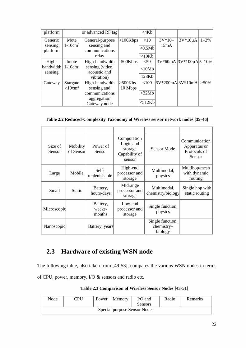
Table 2.1 Four Classes of Sensor-Network Nodes [39-46].
Node Type Name
and Size
Application
Sensors
Radio
Bandwidth
MIPS
Flash
RAM
Active
Energy
(mW)
Sleep
Energy
(µW)
Duty
Cycle
(%)
Specialized
sensing
Spec
mm2
Specialized low-
bandwidth sensor
<50Kbps <5 1.8V*10–
15mA
1.8V*lµA 0.1–
0.5% <0.1Mb
22
platform or advanced RF tag <4Kb
Generic
sensing
platform
Mote
1-10cm3
General-purpose
sensing and
communications
relay
<100Kbps <10 3V*10–
15mA
3V*10µA 1–2%
<0.5Mb
<10Kb
High-
bandwidth
sensing
Imote
1-10cm3
High-bandwidth
sensing (video,
acoustic and
vibration)
-500Kbps <50 3V*60mA 3V*100µA 5–10%
<10Mb
128Kb
Gateway Stargate
>10cm3
High-bandwidth
sensing and
communications
aggregation
Gateway node
>500Kbs–
10 Mbps
<100 3V*200mA 3V*10mA >50%
<32Mb
<512Kb
Table 2.2 Reduced-Complexity Taxonomy of Wireless sensor network nodes [39-46]
Size of
Sensor
Mobility
of Sensor
Power of
Sensor
Computation
Logic and
storage
Capability of
sensor
Sensor Mode
Communication
Apparatus or
Protocols of
Sensor
Large Mobile Self-
replenishable
High-end
processor and
storage
Multimodal,
physics
Multihop/mesh
with dynamic
routing
Small Static Battery,
hours-days
Midrange
processor and
storage
Multimodal,
chemistry/biology
Single hop with
static routing
Microscopic
Battery,
weeks-
months
Low-end
processor and
storage
Single function,
physics
Nanoscopic Battery, years
Single function,
chemistry–
biology
2.3 Hardware of existing WSN node
The following table, also taken from [49-53], compares the various WSN nodes in terms
of CPU, power, memory, I/O & sensors and radio etc.
Table 2.3 Comparison of Wireless Sensor Nodes [43-51]
Node CPU Power Memory I/O and
Sensors
Radio Remarks
Special purpose Sensor Nodes

23
Spec
2003
4–8Mhz
Custom 8-bit
3mW
peak
3µW
idle
3K RAM IO Pads on
chip.
ADC
50–
100Kbps
Full custom
silicon, trade
RF range and
accuracy for
low-power
operation
Generic Sensor Nodes
Rene
1999
ATMEL
8535
.036mW
sleep
60mW
active
512B-
RAM 8K
Flash
Large
expansion
connector
10Kbps Primary
TinyOS
development
platform
Mica-2
2001
ATMEGA
128
.036mW
sleep
60mW
active
4K RAM
128K
Flash
Large
expansion
connector
76Kbps Primary
TinyOs
development
platform
Telos
2004
Motorola
HCS08
.001mW
sleep
32mW
active
4K RAM USB and
Ethernet
250Kbps Supports IEEE
802.15.4
standard.
Allows higher
layer Zigbee
stardard.
1.8V operation
Mica-Z
2004
ATMEGA
128
4K RAM
128K
Flash
Large
expansion
connector
250Kbps Supports IEEE
802.15.4
standard.
Allows higher-
layer Zigbee
stardard.
High-bandwidth Sensor Nodes
BT Node
2001
ATMEL
Mega 128L
7.328Mhz
50MW
idle 285
MW
active
128KB
Flash 4KB
EEPROM
4KB
SRAM
8-channel 10-
bit
A/D, 2
UARTS
Expandable
connectors
Bluetooth Easy
connectivity
with cell
phones.
Supports
TinyOS.
Multihop using
Multiple
radios/nodes
Imote 1.0
2003
ARM
7TDMI 12-
48MHz
1mW
Idle
120mW
Active
64KB
SRAM
512KB
Flash
UART.USB.
GPIO.I2C.SPI
Bluetooth
1.1
Multihop using
scatternets,
easy
connections to
PDAs. Phones,
TinyOS
1.0.1.1.
Gateway Nodes
Stargate
2003
Intel
PXA255
64KNSRM 2PCMICA/CF.
com ports.
Ethernet, USB
Serial
connection
to sensor
network
Flexible I/O
and small form
factor power
management.
Inrysnc
Cerfcube
2003
Intel
PX4255
32KB.
Flash
64KB.
Single CF
card.
general-
Small form
factor,
Robust

24
SRAM purpose
I/O
industrial
support, Linux
and
Windows CE
support.
PCI04
Nodes
X86
Processor
32KB
Flash
64 KB
SRAM
PCI Bus Embedded
Linux or
Windows
support.
EmberNet
2005
Atmega128L - 4KB
SRAM
128KB
Flash
Ember250 Ember
IP-Link MSP430 - 10KB
SRAM
48KB
Flash
CC2420 Helicomm
Spot ARM - 64KB
SRAM
512KB
Flash
Bluetooth CC2420 Sun
Zbnode ARM - 64KB
SRAM
512KB
Flash
Bluetooth CC2420 Taiwan ITRI
XYZ
2007
ARM - 64KB
SRAM
512KB
Flash
Bluetooth CC2420 Yale
WINS
2008
PXA255 - 256KB
SRAM
32KB
Flash
2.4 Ghz 802.11b Sensoria
Embernet ATmega1281 - 128KB
Flash 4KB
EEPROM
4KB
SRAM
2.4 Ghz Ember250 Ember
Cicada1
2010
MC9S08GT60 - 4KB
SRAM
60KB
Flash
2.4 Ghz MC13193 Tsinghua
Cicada2
2011
MC13193 - 4KB
SRAM
60KB
Flash
2.4 Ghz MC13193 Tsinghua
2.4 Issues with wireless sensor network nodes
2.4.1 Reliability:

25
Problems with batteries running out cause WSN nodes to be lost. This results
in uncovered areas in the network at the areas where the batteries of WSN
nodes are drained out. The possibility of data getting lost also exists if a
WSN node cannot connect to other WSN nodes in the network to pass along
information, highlighting the importance of robust design and longer life
[54-59].
2.4.2 Importance of Energy Management
In most of the applications WSN nodes are deployed in remote geographical
locations and often it is difficult to replace the batteries once the nodes are
deployed in the field. Therefore the efficient energy management plays a
significant role in optimizing the lifetime of a WSN node. For example in
agricultural applications, it is not practically feasible to replace the batteries
or perform any type of maintenance on WSN nodes. The cost involved in the
replacing batteries of nodes is another important consideration which poses
restriction on maintenance of nodes once deployed. Further when there are
thousands of WSN nodes deployed it is not practically viable to have to be
concerned with the maintenance of a given WSN node [60-63]. Therefore
WSN nodes are designed to be disposable, making it more cost effective to
deploy additional new nodes rather than replace batteries in existing nodes.
Therefore most of wireless sensor network applications require the WSN
nodes to be operational for many years. It is thus essential that the WSN
nodes are reliable and work on their own for the complete duration of the

26
application. If in a network a large number of WSN nodes become unusable
due to dead batteries or maintenance requirements then the reliability of the
network is affected significantly [64-67].
2.4.3 Methods of Energy Management
Energy management techniques are those that reduce power consumption of
some components of the node or the entire node. The tradeoff between
energy savings and latency are of major concern. Sometime critical
applications cannot tolerate delay delivery of the sensed data.
2.4.3.1 Using data reduction techniques
It is desirable to reduce the amount of data that needs to be transmitted
between nodes because transmission consumes a lot of power. Data
aggregation methods are used to minimize the amount of redundancy in the
data that needs to be transmitted. Although the processor consumes power
during this process, it is much less than that consumed by the transmitting
and receiving tasks [68].
2.4.3.2 Nodes switch between active (on) and sleeping (off)
mode
Different studies have been carried out that involve nodes switching between
an active and sleep mode [69]. The parameters include how to determine the
active/sleep schedule, the duration of the active/sleep period, and whether or
not the nodes are aware of the schedules of the other nodes in the network.

27
In order for the network to be reliable, events must not be missed. The
nodes should be designed in a way such that even during the sleep mode
nodes should be able to detect the desired events as per the requirement of
application [70].
2.4.3.3 Nodes are independent
In a typical application several nodes are deployed. All of these nodes are
not in active mode for complete operational duration. The nodes are
switched between active and sleeping mode independently of each other.
Nodes are responsible for sensing a particular area and sending data to the
base node by using other nodes as communication link to relay the message.
The base node is always connected and in active mode. Other nodes spend
more time sleeping than in active mode [71].
When a node detects an event of interest it becomes active. This node then
starts sending the signal to all the neighboring nodes alerting them so that
they comes in active mode and become ready to receive the signal. The node
keeps transmitting the information until all of its immediate neighbors are in
active mode, since they can only receive the message and relay it to the base
station only if they are awake.
When all the neighboring nodes are in active mode and the event of interest
has been properly detected and relayed to the base station through
neighboring nodes. The nodes can resume their original process of switching
between active and sleep modes until the occurrence of the next event of

28
interest takes place, in case of which the complete process described above
will be repeated.
One major problem in using this scheme is the delay (latency) introduced by
a message trying to reach a sleeping node. Latency is acceptable in some
applications such as those that gather statistical information. Time critical
applications such as those that send an alarm when an unexpected event
occurs are much less tolerant of latency [70].
Latency is affected by random placement of the nodes, random radio range,
sensing distance, random sleeping and active periods of the nodes. Even
applications that can tolerate latency would not tolerate a high degree of
variability in the amount of latency. The latency will be larger as the node
gets farther away from the base node.
Since the information is relayed from the particular location where the event
of interest has taken place to the base station therefore the delay or latency is
proportional to the distance of the base station form the node which has
detected the event of interest. In many applications latency is not an
important factor and it can be compromised to improve the power
consumption and the lifetime of WSN node.
Table 2.4: Various states of the wireless sensor network node
State SA-1110 Sensor, A/D Radio
Active (S0) active sense tx/rx
Ready (S1) idle sense rx

29
Monitor (S2) sleep sense rx
Observe (S3) sleep sense off
Deep Sleep (S4) sleep off off
Table 2.5: Sleep state power, latency and thresholds
State Power (mW) Time (ms) Threshold time(ms)
Active 1040 - -
Ready 400 5 8
Monitor 270 15 20
Look 200 20 25
Sleep 10 50 50
If a node is in a deep sleep state energy saving will be more, and the wakeup
time will be longer. While putting the node to sleep state care must be taken
to make sure that more energy is not consumed by putting the node to sleep
and waking it up than leaving it awake constantly[49].
2.4.3.4 Event based communication
In the event based communication model nodes are in sleep mode. Nodes
becomes active only in the case if they detect the occurrence of the event of
interest has taken place. Each node is designed to receive, transmit and
process the data and power its radio down to a low-power sleep mode. An
event detector periodically alerts the node to sample the data for the
detection of the event of interest. There is a master node which serves as the
base station. Since the master node should remain connected and in active

30
mode all whole duration of operation. Therefore a master node is designed
with the greater computational, transmission and storage capability. Other
nodes are generally kept in sleep mode and they optimize the power
consumption by only responding or becoming active only during the
occurrence of the event of interest
2.4.3.5 By reducing the coverage area
The nature and the criticality of particular application determine the
frequency of the sensing activity therefore it is difficult to optimize or reduce
the sampling frequency of the node. The amount of energy consumed by a
WSN node is directly dependent upon the size of area covered by it [68].
Therefore by reducing the coverage area of a WSN node its power
consumption can also be reduced. To compensate the coverage of the area
per node, the number of WSN nodes used by the application requires to be
increased. This will result in significant improvement in the lifetime of a
particular wireless sensor network node.
2.4.3.6 Scavenging Energy
The amount of power consumed by the processing and communications
tasks is also dependent on the hardware. The Berkeley Wireless Research
Center PicoRadio project is trying to reduce energy consumption in Wireless
Sensor Networks by concentrating on the hardware. One method they are
exploring is using custom RF integrated circuitry to scavenge energy from
other resources such as solar and vibration sources. A study by [69-70]

31
indicates that 100% of the necessary power can come from the sun, while
vibration can contribute about 2.6% of the needed power [71].
2.5 Literature survey of WSN for agriculture applications
There are no examples of commercial applications of WSN in agriculture
applications to date. However, in recent years a number of investigations
have been conducted by scientists in realistic agricultural settings. In 2004,
Beckwith et al. [72] reported on the use of sensor networks for integrated
management of a vineyard. They first assessed the needs of vineyard
managers for designing and deploying a WSN system in the field. To
maintain the desired temperature in the field, this is necessary for the
development of grapes for good quality of wine [73]. Earlier than 2004
because of the high costs of environment monitoring, most vineyard owners
used single sensor for vineyard monitoring purpose. Field work was
conducted by Beckwith et al.[73]. 48 nodes were deployed over a period of
more than 6 months in an Oregon vineyard, reporting temperature every five
minutes. The results were logged at centralized place and could be displayed
on a map and retrieved on a per-sensor basis. Moreover, alarms were sent
when the temperature decreased below 0oC, indicating a risk of frost. The
history of the temperature variations throughout a cropping season is
especially critical. Variation in fruit maturity within a management block is a

32
well-known phenomenon and vineyard owners adapt their harvesting
strategy accordingly.
In 2006, Pereira [74] presented the results of the monitoring of climate in a
crop field. The deployed nodes monitored humidity and temperature in order
to better fight phytophtora in a potato field. In Pereira’s words, phytophtora
is a fungal disease which can enter a field through a variety of sources. The
development and associated attack of the crop depends strongly on the
climate conditions within the field. Humidity is an important factor in the
development of the disease. His aim was to predict the disease and to
schedule fungicide treatment to prevent disease. The authors only reported
on the pilot study, however. The full-size network has not been deployed yet.
Ahonen et al. [75] in 2008 developed a small wireless sensor network in
order to monitor the emergence of certain diseases in a greenhouse: gray
mould, leaf mould and powdery mildew. The goal was to explore the
potential of WSNs for the control and maintenance of temperature, humidity
and CO2 concentrations within optimal limits. Bishop-Hurley [76] explored
the potential of wireless sensor networks for nationwide cattle monitoring
systems at farms. Each wireless sensor acts as an extended RFID collar
storing the identity and health status of the cattle, which can be tracked at
different locations, such as pasture or farm buildings. Each location is
equipped with a base station recording the information from the collars as

33
the cattle come into its range. The system was evaluated through extensive
rounds of simulations.
Bishop-Hurley et al. [76-78] also tested the responsiveness of cattle to
electrical and audio stimuli designed to modify their behavior and prevent
them from crossing a line in an experimental alley. Cattle were equipped
with collars containing a GPS receiver for positioning and a wireless
transceiver similar to a wireless sensor. Each collar communicated to a base
station connected to a server responsible to analyze the received signals and
to generate the appropriate cues. The goal was to design a virtual fencing
application replacing expensive wired fences in extensive grazing systems.
Hirafuji et al. [79] developed the concept of Field-Monitoring Server, a Wi-
Fi based wireless sensing platform that was applied in settings as various as
Earth observation, urban image monitoring and agriculture. They report on
the deployment of a network of 5 nodes in paddy fields [78]. They stated that
agricultural monitoring systems need enhanced capabilities, such as wireless
broadband communication and high-resolution image-monitoring
technology. In their words, “specific data such as images of emerging rice
blast are indispensable to revise the prediction system” [80]. However,
concrete results on how to process this information and for what benefit have
not been published yet.
Precision agriculture has been using state-of-the-art sensors for decades.
However, the possibilities offered by environmental monitoring were limited

34
due to the infrastructure and the labor costs it incurred. In this section, we
have presented four typical projects in the area of wireless sensor networks
for agriculture. Although it is generally admitted that fine-grained
environmental monitoring holds great promise for agricultural sciences,
related projects are still few in the scientific literature [80-83].
A possible explanation is that the wireless sensor networking is just reaching
its maturity phase. Some work done on WSNs in environmental monitoring
in general have finally demonstrated the feasibility of deploying and
maintaining such networks for periods of time in the order of a few months.
Such endeavors were a prerequisite to the collection and analysis of the
amount of data necessary to develop useful applications for agriculture.
Another observation is that most of the projects were focused on few and
simple data measurements, usually air temperature and humidity. A possible
explanation is that such sensors come as standards on most platforms, which
makes them easy to use. Whereas, the soil moisture probes for wireless
sensors network required until recently the design of special data acquisition
boards, and in most cases needed to be properly calibrate for WSN use [84].
A closer look at the individual projects leads to the following observations.
Firstly, event-detection emerges as a strong theme in the envisioned
applications. Two of the projects deal with early detection of diseases, one
with prediction of frost, and one with virtual fencing (i.e., redirecting cattle
when they risk to leave their grazing area). In all these applications, the
35
capacity of wireless sensor network to report events in real-time is
emphasized. In two occurrences, vineyard and paddy field monitoring,
continuous monitoring is also used to adapt farming strategies, in the short or
long term. In all cases, spatial and time fine-grained resolutions are
perceived as a critical improvement.
Secondly, most of the networks focus on sensing rather than actuating. The
goal is to provide the user with enhanced information that lets him take his
own decision. Only for cattle monitoring is the sensor coupled with an
actuator, namely an audio or electrical stimulus.
As for a power source, batteries are used in most cases, for different reasons.
In vineyard monitoring, the constraint was to deploy light-weight sensing
nodes on the vines themselves. Solar panels would be difficult to adapt in
this situation, because of their size and the effect of vegetation on solar
energy collection over time. Similar concerns were probably considered by
Bishop-Hurley et al. [76], as solar panels would be problematic to install on
cows’ collars. The tomato disease prediction application is aimed at
greenhouses, where solar energy is not directly available.
Finally, the size of the networks remains small, in the order of a few tens of
nodes in the largest case. This indicates both the investigative nature of the
experiments, which are primarily aimed at research rather than production,
and the scalability challenges raised by WSNs to this day. In particular,
Beckwith et al. [73, 77] acknowledge resorting to a planned network

36
configuration rather than a self-organizing one, for deployment facilitation.
Such an approach would not scale to large networks.
To summarize briefly, we can consider these projects as proofs of concepts,
whose transposition to commercial products will be the measure of success
in years to come. This situation is likely to change, as proper commercial
tools are soon going to be in the hands of agricultural scientists. Tim Wark et
al. [85, 86] deployed a network of 16 of such nodes equipped with ECH2O
soil moisture probes in order to observe the effects of irrigation on
agricultural plots.
2.6 Objectives
The basic objective of the study has been to assess the various factors
affecting the lifetime of wireless sensor node. The objective of this thesis
was to design and develop a low power wireless sensor network node for
agricultural application. The main aim was to minimize power consumption
and overall power management in such a way to increase the lifetime of a
WSN node. There are four major units of wireless sensor network node (as
discussed in chapter one) a power unit, a sensing unit, a processing unit, and
a transmission unit. The power consumption of WSN node can be optimized
by reducing the power consumption by any or all of these four units. In this
thesis the processing unit has been optimized to reduce the overall power
consumption of the WSN node. For this the processing unit has been custom

37
designed for a WSN node for agricultural application. The architectural
details of processing unit are further discussed in detail in chapter 4.
Designing such an efficient system is a highly challenging task that requires
new approaches in many different aspects of the whole system design and
even the design methodology itself. A low power node will not require the
frequent replacement of batteries during the lifetime.
The basic objective of the study has been to assess the impact of:
Evaluation of wireless sensor network and WSN node hardware.
Assessment of the validity of use of WSN node in agriculture
application.
Designing customized event processor for WSN Node.
Developing a low power WSN node specifically for agriculture
application.
Evaluation of the effect of the custom designed processing unit of
agriculture application-dependent WSN node on enhancing the
lifetime of a WSN node.
2.7 Research Approach and Strategy
The figure 2.2 depicts research is carried out through problem identification,
approach and strategy adopted for solving the problem.

38
Figure 2.2 Research approach and strategy
Our study is exploratory as the reader become familiar with the basic facts,
setting and concerns. It also formulates and focuses on question for future
research, generate new ideas and hypotheses. The study is also descriptive as
it clarifies a systematic study of wireless sensor network nodes, its
applications, its role in agriculture application and the known issues in
wireless sensor nodes. It is explanatory as we have carried out hardware trial
of wireless sensor node and also tested wireless sensor node through
simulation.
In research, different approaches can be taken such as deductive or inductive,
and qualitative and quantitative. The existing papers and research work were
studied thoroughly by us and then the formulation of hypothesis was done

39
which suggest that the research approach was deductive in nature. As the
purpose of this study is to enhance the overall lifetime of wireless senor node
the selection of appropriate section of WSN node was done to fulfill the
stated purpose of reducing power consumption and increasing overall
lifetime of wireless sensor node. In addition, as this study is intended to
explore, describe and find information as much as possible, the qualitative
approach is found the most appropriate. At later stage hardware of WSN
node was designed and tested this shows our approach is quantitative as
well.
In carrying out this study, the answers of the following questions have been
found and investigated:
What is WSN and what are the major areas and applications of WSN
node?
How can WSN nodes be used in agricultural applications and what is
their existing use?
How the overall lifetime of WSN node can be maximized, what
parameters effect the power consumption of WSN node?
The survey strategy was chosen for finding the existing facts and difference
between them (comparison). The literature survey of WSN its applications,
its hardware and agricultural application of WSN node was carried to decide
research strategy. The investigations, simulations and hardware trials were
carried out to support the chosen strategy.

40
2.8 Thesis outline
The thesis presents the results of study and findings on implementation and
design of a low power WSN node. The area considered for research id
limited to the agricultural application that means lower clock frequency for
processing unit and tolerance to latency. The main thrust of the work
reported in this thesis has been on developing custom designed low power
processing unit for the WSN node.
The thesis is divided in to six chapters which described the thesis as follows:
Chapter-1 starts with the introduction of wireless sensor networks (WSN)
and components of a sensor node. Further the overview of WSN and its
applications are given. Followed with the discussion of requirements and
design factors in wireless sensor Networks. Each design factor is described.
From this chapter, we had one publication in international journal and one
publication in conference.
Chapter-2 gives the WSN background and the related work. Starting with
introduction the chapter deals with importance of WSN and its
characteristics like size, power consumption, cost, lifetime, ease of
deployment, Response time, security and sample rate etc. then a
classification of WSN nodes is given along with comparison. Then the
components of a WSN node are described along with potential problems

41
with WSN. The potential problems in WSN like path obstruction &
reliability are discussed. Thereafter the issue of energy management, its
importance; methods of energy management are discussed. Then a
comparison of sensor network node Hardware is given in tabular form
followed by system specifications for a sample Node. Chapter is concluded
with thesis objective, contributions and detailed thesis outline.
Chapter- 3 describes the construction of Hardware of WSN node. The
chapter starts with overall system specifications including specifications for
processor subsystem, RF subsystem and sensor subsystem. Then a detailed
description of modular design of processor & it’s essential blocks like
memory, watchdog times UART, interrupts and Power sensor subsystem &
its parts like Humidity sensor, temperature sensor & PH sensor are given and
finally RF subsystem details are discussed at the end the complete circuit
diagram of the WSN node with its working is given. From this chapter we
had two publications in international journal. We had one publication in
conference from this chapter.
Chapter-4 covers the system architecture design for wireless sensor node.
The chapter starts with overview of system architecture along with a block
diagram covering each unit i.e. sensing unit, processing unit and transmitting
unit in detail. A special focus is given the custom designed processing unit
for the WSN node, each block of the processing node is discussed in detail

42
along-with its signal name, signal type and description a complete
architecture of the custom designed processor for WSN node is also
followed by the discussion of the transceiver section.
Chapter-5 starts with an introduction to the design implementation of WSN
node. Followed by the description RTL View, results verification waveforms
of the various blocks of custom designed event processor. Then a
comparison of proposed nodes custom designed processor with other
existing nodes processor is done. Finally the comparison of the power of
proposed node with existing nodes is given. There is another international
publication from this chapter.
Chapter-6 concludes the work and presents the scope for future work in
detail.
At the end, a systematic bibliography and list of references of all the text
books, research papers, monographs, etc. used in thesis are given.
Finally, an Appendix B containing synthesis report and Appendix C
containing VHDL code for the custom designed event processor is given.
2.9 Summary of the chapter
In this chapter, we discussed the literature review, issues related to design
and implementation of WSN node. We also discussed the methodology
employed to address our research problem and research questions were

43
discussed. The research purpose, approach, strategy implementation
approach were presented, discussed and justified.

44
CHAPTER 3:
Design and Implementation
of WSN Node
Design and Implementation
of WSN Node is done and
which is presented in the chapter
Hardware Implementation of WSN Node
and power estimation is done. The design
and implementation are discussed in the
chapter.

45
CHAPTER 3: Design and Implementation of WSN
Node
3.1 Introduction
The aim was to design a prototype of WSN Node using easily available
discrete components. The various components required for the development
of prototype were surveyed. The need to first design a WSN node made of
commercially available components was realized and the current work is
channeled towards that objective. A survey of various existing nodes was
undertaken and the evolution of the node hardware was understood and
discussed in the previous chapter. Then a basic configuration of a wireless
sensor node was designed and the components were identified. A tentative
circuit layout has been designed.
Now that attempt is to design an individual node with a goal to evaluate
performance of a sensor node made of commercially available components
[87].

46
3.2 Design of WSN node
A typical Wireless Sensor Networks node has the task of sensing, processing
and communicating the data. WSN node requires several components to
accomplish these tasks. Each of these components can be considered
separately, they can be managed separately, in different subsections or
subcomponents allowing better energy management [88].
The block diagram of prototype of WSN node is given in figure 3.1. Various
WSN node subsystems and their designs are discussed in the following
subsections.
Figure 3.1: Block Schematic of the subsystems of WSN node
Different modules of the WSN node along with their specifications are
shown in figure 3.2.

47
Figure 3.2: Block Schematic Overview of the subsystems of WSN node
WSN node system design requirements are as follows:
1. Two signals – Temperature and Humidity, are to be sensed
periodically, Bandwidth of the signals is at a maximum of 1Hz.
2. Terminal voltage of battery for System – 5V.
3. Wireless Transceiver operating at ISM band (2.4-2.483GHz).
4. The System must operate at minimum power requirement.
5. The node must also act as a repeater/router.
6. The whole design must be compact and light-weight.
In the following sections each system subsection/ module of WSN node, its
design and other features are given in detail [89-92].
3.3 Sensor Subsystem

48
There exists a large variety of low power sensors suitable for WSNs [93].
For example, sensors are available for acceleration, air pressure, humidity,
illumination, infra-red, magnetic field, geographic position, and temperature.
Important requirements for sensors are low power consumption and short
sensing time, which determine the energy consumption of a single sensing.
In addition, adequate accuracy is required within the entire temperature
range. The features of some example sensors are presented in Table 3.1.
Table 3.1 Features of typical sensors.
Physical quantity Example sensor Accuracy Active
Current
Sensing
time
Acceleration VTI SCA 3000 1% 120 μA 10 ms
Air pressure VTI SCP1000 150 Pa 25 μA 110 ms
Humidity Sensorion SHT15 2% 300 μA 210 ms
Magnetic field Hitachi HM55B 5% 9.0 ma 30 ms
Position Fastrax iTRAX03 1.0m 32 mA 4.0 s
Temperature Dallas DS620U 0.50C 800 μA 200 ms
Most of the sensors fulfill the requirements well. A WSN node can also
operate as a decision unit, which takes sensor readings as input and generates
action commands as output. The prototype of WSN node is designed to
measure two physical parameters i.e. humidity and temperature [94-98].
Therefore the sensor subsystem of WSN node employ two sensors namely a
humidity sensor and a temperature sensor. Detailed description of the

49
sensors used in sensor subsystem, their design requirements etc. are given in
the following sections.
3.3.1 Humidity Sensor
The prototype WSN node uses a conventional sensor and a microcontroller
that can process the data acquired using algorithms to reduce the amount
of data collected, to extract only relevant information and to present this
information in a format which minimizes the amount of data to be
transmitted. As a result of which the final processing end has to perform a
little computation that too only on features like significant changes in
humidity rather on the huge data hence reducing the power consumption
[99]. Further the prototype WSN node reduces the amount of data
processed by 50% (depending upon humidity variations) and thereby also
reducing the power consumption.
The most common problems that are involved with the conventional
humidity sensors used in WSN node in agricultural applications is generation
of large amount of data to be processed/transmitted, which consumes large
amount of power from a small battery operated WSN node. Other associated
problem is of corrosion of the connectors due to moisture, extreme/sudden
temperature changes etc.
A calibration table is stored in the memory of processing subsystem of WSN
node. In this calibration table the pre-acquired different standard reference
values of capacitances are stored in the memory map (look up table) for

50
processing by the processor of WSN node. That is, the humidity sensor uses
the look up table stored in the memory of the embedded processor for
displaying the calibrated reading of soil water tension. This WSN node
employing humidity sensor can play a significant role in soil moisture
measurement technology and hence can be very useful for the precision
agriculture [100-102]. The WSN node with humidity sensor is an ideal
solution for both agricultural and landscape applications. Its electrical
characteristics make it ideally suited to use with central master/base station
electronic data processing equipment for collecting and processing data from
various sensors deployed in agriculture field for precision agriculture
applications [103].
A capacitance type humidity sensor is selected here as the sensing element in
the WSN node design. A capacitance type humidity sensor detects changes
in humidity by measuring the change in the electrostatic capacity of an
element relative to the ambient humidity [104]. Capacitive moisture meters
deliver a capacitance value with respect to the air humidity in the area
around the measuring element. The value of the capacitance can be estimated
with the help of digital measurement techniques. A particular moisture value
is confirmed with the measured capacitance value, using further look up
table and other comparative parameters [105]. Humidity sensing elements of
the capacitance sensing type sensor, usually consist of moisture resistive,
non-conducting design with an electrode made up of layer or coating of

51
dielectric. The coating used for the dielectric is generally very highly
moisture-sensitive. Electrodes are positioned such that they are able to
absorb water from the surrounding atmosphere easily in short duration of
time. This type of humidity sensors are fabricated by depositing layer of
dielectric material on a substrate. This type of humidity sensors does not
show a linear relationship between the capacitance and humidity. Therefore
they require calibration to compensate this nonlinearity. For the calibration
purpose reference data obtained from Honeywell HCH 1000 series air
humidity sensor was used [106]. Figure 3.3 depicts the circuit schematic of
the capacitive sensor used for simulation of humidity sensor of WSN node
before actual hardware trial.
Figure 3.3 Circuit schematic of capacitive sensor
Capacitance is measured by applying 1 Vrms at 20 kHz at 25 °C. The sensor
characteristic is determined by the following formula [106]:
CC (%RH) = CS at 55%RH + S x [(%RH (CM ) - %RH(CS )]pF (3.1)

52
Where S is Sensitivity (pF/%RH), CC is (%RH) calculated capacitance at the
measured relative humidity, CS at 55 %RH is standard capacitance value at
55% RH, %RH(CM) is measured relative humidity value, %RH(CS) is
standard relative humidity value (55%RH).
% RH(CC ) = C M (%RH) - CS at 55%RH + % RH(CS ) (3.2)
S
The average increase in capacitance value within the working range of 10%
RH to 95% RH is typically 56 pF.
The HIH-4030 Series Humidity Sensor is chosen in the design of WSN node
prototype. It is chosen due to the following of its characteristics:
• Molded plastic housing.
• Near linear voltage output vs %RH.
• Laser trimmed interchange ability.
• Low power design.
• Enhanced accuracy.
• Fast response time.
• Stable, low drift performance.
The HIH-4030 series humidity sensors are designed specifically for high
volume OEM (Original Equipment Manufacturer) users. HIH-4030 gives
almost linear voltage output therefore its output can be given directly to the
input of a controller or other device. Since it draws very little current about
200 μA therefore it is well suited for low drain, battery operated WSN nodes.
Close sensor compatibility reduces production and calibration costs.

53
Individual sensor calibration data is available. The selected sensor gives very
good relative humidity (RH) sensing performance suitable for use in a WSN
node. The HIH-4030 is a closed IC based humidity sensor [106-109].
Figure 3.4 Humidity sensors
The HIH-4030 sensor uses a thermoset polymer type capacitive element for
sensing. It is also having on-chip integrated signal conditioning capabilities.
The special multilayer design of this polymer type capacitive sensing
element makes it very robust. It also provides the sensor very good corrosion
resistance. The sensor is almost insensitive to typical WSN application
hazards such as corrosion and deterioration caused by dust, grit, water, soil
and other common chemicals present in an agricultural field.
Table 3.1 Performance specifications of humidity sensor HIH-4030
Parameter Minimum Typical Maximum Unit
0% RH to 59% RH -5 _ 5 0%RH
60% RH to 100% RH -8 _ 8 0%RH
Accuracy -3.5 _ 3.5 0%RH
Hysteresis _ 3 _ 0%RH
Repeatability _ 0.5 _ 0%RH
Settling time _ _ 70 ms

54
Voltage supply 4 _ 5.8 Vdc
Current supply _ 200 500 µA
3.3.2 Temperature Sensor
Measurement of temperature is critical in modern electronic devices. A
temperature sensor produces a voltage that is proportional to the ambient
temperature sensed. This voltage is supplied as one of the single-ended
inputs to the Analog to Digital Converter (ADC) converter [110]. The
LM35 is an integrated circuit that provides a linear output proportional to
temperature, with a sensitivity of 10mV per degree Celsius. It does not
require any external calibration or trimming and provides typical
accuracies of +/- 0.25 degrees at room temperature and +/- 0.75 degrees
over a full -55 to +150 degrees C temperature range. It is available in a
number of different packages, e.g. TO-46, TO-92, 8-lead surface mount
SO, and TO-220.
To simulate this device in SPICE, such that it produces the normally
expected voltage output at any given temperature, a linear temperature
controlled element is required. There is an option for the resistor model to
specify a temperature coefficient, or a polynomial series of temperature
coefficients [111]. A current source and a resistor can be used to create a
voltage source that has a linear temperature coefficient. The resistor has a
value:
R = R0 (1+ dt.tc1) (3.3)

55
where R0denotes the value of resistance at the minimum temperature,
dt denotes the change between the resistor's temperature andR0, and
tc1denotes the temperature coefficient.
LM-35 is calibrated to give zero output voltage at designated
temperature. Therefore another current source and resistor are used to
generate a voltage corresponding to a fixed temperature at 0oC [112]. A
voltage-controlled current source G1 is used to subtract the reference
voltage from the temperature dependent voltage to obtain a temperature
dependent output that is zero at the reference temperature for the LM-35.
The gain of G1 and its shunt resistor are chosen to give a voltage gain of
1 and an output impedance of 0.1 ohms to match the dynamic impedance
of the LM-35 for a 1mA load.
This simulation uses the built-in global temperature value of SPICE that
is generally used to specify the operating temperature of a circuit. It is
also used to measure characteristics of the circuit over a given
temperature range [112-115].
Figure 3.5 shows the simulation model for the temperature sensor. The
circuit given in figure 3.5 is purely a behavioral model. It requires a pull-
down resistor for the coverage of full sub-zero temperature range.

56
Figure 3.5 Simulation model for LM-35 Series temperature sensor
After the simulation, the LM-35 Series Temperature Sensor is chosen for the
prototype of WSN node. It is chosen due to the following of its
characteristics:
The output voltage is proportional to temperature.
The output of LM-35 is directly calibrated in degrees Celsius.
It has a guaranteed accuracy of 0.5 ° C to 25 ° C.
It has low output impedance.
It gives linear output.
It has precise inherent calibration.
It is easy to interface to readout or control circuitry.
It can be used with single power supplies, or with plus and minus
supplies.
It is low cost since it does not require calibration.
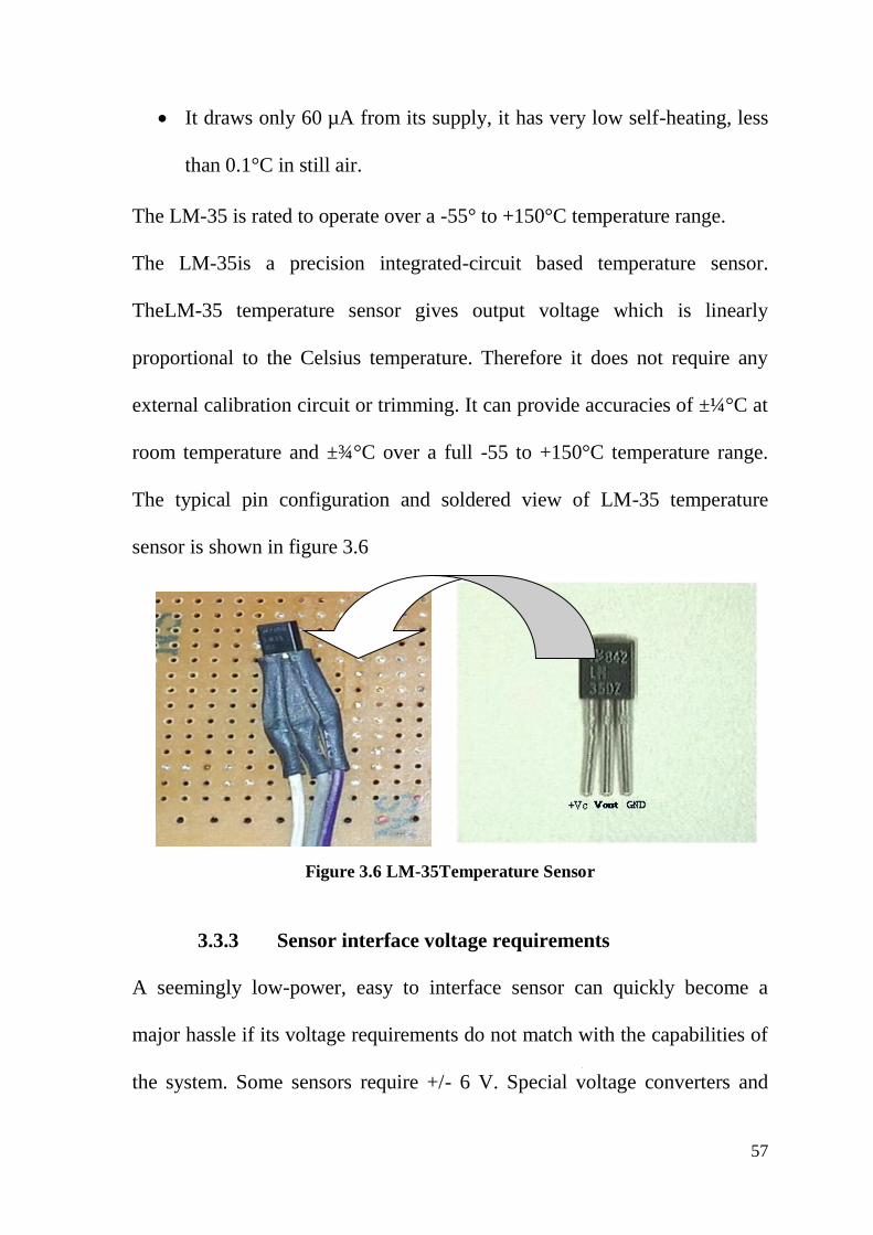
57
It draws only 60 µA from its supply, it has very low self-heating, less
than 0.1°C in still air.
The LM-35 is rated to operate over a -55° to +150°C temperature range.
The LM-35is a precision integrated-circuit based temperature sensor.
TheLM-35 temperature sensor gives output voltage which is linearly
proportional to the Celsius temperature. Therefore it does not require any
external calibration circuit or trimming. It can provide accuracies of ±¼°C at
room temperature and ±¾°C over a full -55 to +150°C temperature range.
The typical pin configuration and soldered view of LM-35 temperature
sensor is shown in figure 3.6
Figure 3.6 LM-35Temperature Sensor
3.3.3 Sensor interface voltage requirements
A seemingly low-power, easy to interface sensor can quickly become a
major hassle if its voltage requirements do not match with the capabilities of
the system. Some sensors require +/- 6 V. Special voltage converters and

58
regulators have to be added to systems operating on AA or lithium batteries
in order to use the sensor [116-119]. The power consumption and turn-on
times of the regulator, filters etc. are also included in the total energy budget
of the WSN node.
3.4 Processor Subsystem
The central component of a WSN node is a processor unit. The processor
unit is typically implemented using a microcontroller, which integrates a
processor core with program and data memories, timers, configurable I/O
ports, Analog-to-Digital Converter (ADC) and other peripherals [120 -124].
Flash memory is typically used as a program memory, while data memory
consists of SRAM and Electrically Erasable Programmable Read-Only
Memory (EEPROM). WSN nodes utilize typically 1-10 Million Instructions
per Second (MIPS) processing speed. Memory resources typically consist of
1-10 kB of data memory and 16-128 kB of program memory [125]. The
characteristics of potential MCUs from different manufacturers are
compared in Table 3.2.
Table3.2 The comparison of the features of low power MCUs.
MCU FLASH (kB) SRAM (kB) EEPROM (kB) Sleep (μA)
Atmel AT89C51 (8051) 128 8 NA 75
Atmel ATmega (AVR) 128 4 4096 1
Atmel AT91FR40162S
(ARM)
2048 256 NA 400
Cypress CY8C2966 32 2 NA 5
Freescale M68HC08 61 2 NA 22
Microchip PICI8LF8722 128 3.9 1024 2.32
Microchip PIC24FJ128 128 8 NA 21
NA: not available on chip

59
The major task of the processor subsystem is the processing of the data
collected by the sensors. For the efficient power management, the sensors
used in the WSN node are not kept active for all the time but they are
triggered on at regular intervals by the microcontroller. The microcontroller
sends the signal to turn on the sensor for sampling and also subsequently
power to the signal conditioning block of the sensor. Thereby significantly
reducing the overall power consumption in comparison to the system in
which the sensors are always kept active with their signal conditioning
block. Processing subsystem performs the digital linearization and cross-
sensitivity compensation. It uses look-up tables for this purpose. Algorithms
based look-up tables offer good accuracy [126-129]. The microcontroller is
also used to implement smart compression algorithms to extract the relevant
information from the sensor signals. Hence, the amount of information that
needs to be transmitted is decreased. This reduces the power consumption
significantly, since the transceiver or the communication subsystem
consumes maximum power in the sensor node.
The microcontroller was programmed and incorporated in the circuit using
co-simulation feature of NI Multisim –Multi MCU module. A look up table
was prepared and stored in the memory of the microcontroller [130-131].
The microcontroller compared the acquired data with the reference look up
table stored in the memory and processed/transmitted the data only when the
acquired data from the sensor crossed the specified threshold points. This

60
concept can be further extended in such a way that a look up table can be
prepared or updated dynamically by acquiring data from the sensor and can
be compared with recently acquired data, processing will be done only if
there is a significant change between the successive data. AT89S52 of Atmel
Corp. is chosen as the processing unit subsystem [132]. This is having
following characteristics:
• 8MHz, 8 bit
• 128KB In-system reprogrammable Flash memory
• 4KB SRAM
• 32 programmable I/O lines
• Can operate under 2.7 – 5.5 V power supply
The considerations to select this Microcontroller is availability of an
assembler, debugger, compiler and technical support and ready availability
in needed quantities for present and future work.
The microcontroller AT89S52 satisfies the selection criterion necessary for
the
propos
ed
applic
ation.

61
Figure 3.7 General block Diagram of AT89S52microcontroller
The AT89S52 is a low-power, high-performance 8-bitmicrocontroller with
8K bytes of in-system programmable Flash memory [133]. The on-chip
Flash allows the program memory to be reprogrammed in-system or by a
conventional nonvolatile memory programmer. In addition, the AT89S52 is
designed with static logic for operation down to zero frequency and supports
two software selectable power saving mode.
The AT89S52 has following architectural features: it has 8 Kilo bytes of on
chip program memory (Flash) , 256 bytes of data memory (RAM), 4 I/O
ports with eight lines in each port, dedicated Watch dog timer, two special
function registers to act as data pointer(DPTR) , two 16-bit timer/counters,
an interrupt structure which can be cascaded up to two levels and with five
vectored interrupts, a full duplex serial port, on-chip oscillator, and clock
circuitry. In addition, the AT89S52 is designed with static logic for operation

62
down to zero frequency [134]. It can be operated in two program controlled
power saving modes. The Idle Mode stops the CPU while allowing the other
components like data memory, timer/counters, serial port, and interrupt
system etc. to continue functioning. The Power-down mode saves the
contents of data memory but freezes the oscillator, disabling all other CPU
functions until the occurrence of next interrupt service request or hardware
reset [135].
3.4.1 Memory Organization
In general, sensor nodes only require small amounts of storage and program
memory. Data is only stored long enough for it to be analyzed and then
transmitted through the network to the base station. In general, modern flash-
based microcontrollers contain between 1 and 128 KB of on-chip program
storage. This can be used as both program memory and as temporary data
storage. Additionally they contain between 128 and 32KB of data RAM that
can be used for program execution.MCS-51 devices have a separate address
space for Program and Data Memory. Up to 64K bytes each of external
Program and Data Memory can be addressed [136].
3.4.2 Watch dog timer (one-time enabled with reset-out)
The watch dog timer is used in situations where the processing unit is
subjected to programming disturbances. It consists of a 14-bit counter and
the Watch dog Timer Reset (WDTRST) special function register. By default

63
watch dog timer is disabled when microcontroller is reset. To enable the
watch dog timer, 01EH and 0E1H is written in sequence to the Reset register
of watch dog timer. Once the watch dog timer is enabled, it will increment
every machine cycle while the oscillator is running. The watch dog timer
time out period is dependent on the external clock frequency. The watch dog
timer can be disabled only either by hardware reset or by watch dog timer
overflow reset. When watch dog timer overflows, it will drive an output
RESET HIGH pulse at the RST pin.
3.4.2.1 Setting the watch dog timer
To set watch dog timer, a user must write command word 01EH and 0E1H
in sequence to the watch dog timer RST register. Once the watch dog timer
is enabled, it needs to be serviced by writing 01EH and 0E1H to watch dog
timer RST to avoid a watch dog timer overflow. The 14-bit counter over
flows when it reaches 16383 (3FFFH), and this will reset the device. When
the watch dog timer is enabled, it will increment every machine cycle while
the oscillator is running. This means that the watch dog timer must be reset
at least every 16383 machine cycles. To reset the watch dog timer requires
01EH and 0E1H should be written to watch dog timer RST. Watch dog timer
RST is a write – only register. The watch dog timer counter cannot be read
or written. When watch dog timer overflows, it will generate an output
RESET pulse at the RST pin.
3.4.2.2 Watch dog timer during Power – down and Idle mode

64
In Power – down mode the oscillator stops, which means the watch dog
timer also stops. While in power down mode, the watch dog timer does not
requires to be serviced. There are two methods of exiting Power-down mode:
by a hardware reset or via a level-activated external interrupt, which is
enabled prior to entering Power-down mode. To ensure that the watch dog
timer does not overflow within a few states of exiting Power-down, it is best
to reset the watch dog timer just before entering Power-down mode.
3.4.3 UART
The AT89S52’s has an integrated UART which is also known as a serial
port. Due to the availability of integrated serial port it is very easy to read
and write data to the serial port. In absence of a dedicated serial port, sending
data to a serial line would become a very complicated task. It will require
software tosend0 and 1 to one of the I/O lines in rapid succession to properly
send out each individual bit, including start bits, stop bits, and parity bits.
AT89S52 requires only configuring the serial port’s operation mode and
baud rate. Once configured, it only requires SFR to write a value to the serial
port or read the same SFR to read a value from the serial port [137]. The
AT89S52 will automatically indicate when it has finished sending the
character wrote to it and will also indicate whenever it has received a byte.
3.4.4 Timer 0 AND 1
The AT89S52 has Two Timer/Counter of 16 Bits each known asT0 and T1
(Timer 0 and Timer 1).T0 and T1 are used as timers, external event counter

65
etc. They can be easily configured in 4 different modes using Special
function registers.
3.4.5 Interrupts
The AT89S52 has a total of five vectored interrupt. Out of which two are
external interrupts (INT0 and INT1) and other two are used as timer
interrupts (Timers 0 and 1), and the fifth one is used as serial port interrupt.
Each of these interrupt sources can be individually enabled or disabled by
setting or clearing a bit in Special Function Register IE. IE also contains a
global disable bit, EA, which disables all interrupts at once.
3.4.6 Power
An important parameter for power measurement of a microcontroller is the
estimate of its sleep mode power consumption. In a WSN node a CPU is a
major contributor to the node’s standby power consumption. While in idle
condition, the CPU will stop execution and go in to a low-power sleep state.
The processor only requires to maintain its memory and time
synchronization, so that it can properly wake-up whenever it is necessary.
Sleep mode current consumption is around50 µA. This current has a
significant impact on node performance because the CPU is expected to be
idle 99.9% of the time.
3.4.7 Speed
The main tasks of the microcontroller in a processing unit of a WSN node
are to execute the communication between nodes, control the RF subsection

66
(transceiver), apply data compression scheme (if any), communicate with
sensors and perform processing on the data collected by the sensors. Most of
these operations have low speed requirements reducing the overhead of the
controller. The critical variable in determining the necessary computational
speed for a wireless sensor node is the amount of data analysis and in-
network processing that must be performed. The CPU must be capable of
meeting the real-time deadlines demanded by the data processing.
3.5 RF Communication Subsystem
The radio frequency (RF) communication subsystem is another important
sub system of a wireless sensor node. It is one of the primary energy
consumers in almost every application scenarios. Generally low power
transceivers consume approximately the same amount of energy when in
receive or transmit mode. If the receiver is left on 100% of the time during
periods of intermittent communication the power consumption of the RF
subsystem increases drastically.
The communication subsystem consists of a wireless transceiver and an
antenna that is used to transmit and receive data to and from the other nodes.
The tasks to be performed by the transceiver are the selections of a frequency
channel, selection of transmit power, the type of modulation for the
transmitted data and demodulation of received signal, symbol
synchronization and clock generation for received data.
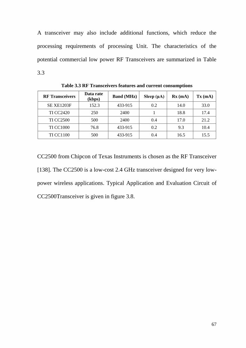
67
A transceiver may also include additional functions, which reduce the
processing requirements of processing Unit. The characteristics of the
potential commercial low power RF Transceivers are summarized in Table
3.3
Table 3.3 RF Transceivers features and current consumptions
RF Transceivers Data rate
(kbps) Band (MHz) Sleep (μA) Rx (mA) Tx (mA)
SE XE1203F 152.3 433-915 0.2 14.0 33.0
TI CC2420 250 2400 1 18.8 17.4
TI CC2500 500 2400 0.4 17.0 21.2
TI CC1000 76.8 433-915 0.2 9.3 10.4
TI CC1100 500 433-915 0.4 16.5 15.5
CC2500 from Chipcon of Texas Instruments is chosen as the RF Transceiver
[138]. The CC2500 is a low-cost 2.4 GHz transceiver designed for very low-
power wireless applications. Typical Application and Evaluation Circuit of
CC2500Transceiver is given in figure 3.8.
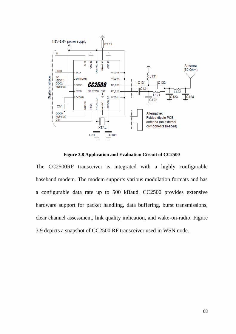
68
Figure 3.8 Application and Evaluation Circuit of CC2500
The CC2500RF transceiver is integrated with a highly configurable
baseband modem. The modem supports various modulation formats and has
a configurable data rate up to 500 kBaud. CC2500 provides extensive
hardware support for packet handling, data buffering, burst transmissions,
clear channel assessment, link quality indication, and wake-on-radio. Figure
3.9 depicts a snapshot of CC2500 RF transceiver used in WSN node.

69
Figure 3.9 CC2500RF transceiver
It has the following functionalities:
High sensitivity (–104 dBm at 2.4 kBaud, 1% packet error rate).
Low current consumption (13.3mAin RX).
Programmable output power upto+1dBm.
Excellent receiver selectivity and blocking performance.
Programmable data rate from 1.2 to 500 kBaud.
Frequency range: 2400–2483.5MHz.
OOK, FSK, GFSK, and MSK supported.
Programmable channel filter bandwidth.
Programmable Carrier Sense (CS) Indicator.

70
Complete on chip components, no external filters or RF switch
needed.
Small size (QLP 4x4 mm package, 20pins).
Support for asynchronous and synchronous serial receive / transmit
mode.
Table 3.4 summarizes the ratings of CC2500 RF transceiver used in WSN
node.
Table 3.4: Absolute maximum rating of CC2500 RF transceiver
Parameter Min Max Units
Supply voltage -0.3 3.6 V
Voltage on any digital
pin
-0.3 3.6 V
Voltage on the pins -0.3 2.0 V
3.6 Power subsystem
The power subsystem stores supply energy and convert it to an appropriate
supply voltage level. The subsystem consists of energy storage, a voltage
regulator, and optionally an energy scavenging unit. As most of the Wireless
Sensor Network nodes are powered by batteries; battery life becomes a
primary design consideration. Maximizing battery life requires to develop an
understanding of the capabilities and limitations of the batteries that power
such systems, and to incorporate battery considerations into the system
design process. The amount of energy that can be supplied by a given battery
varies significantly, depending on how the energy is drawn [139].

71
Consequently, attempt is being made to develop new battery-driven Low
power WSN node, which provides longer battery life over and above what
can be achieved through conventional design techniques. In the prototype
WSN node for testing purpose, power supply section consists of step down
transformers of 230V primary to 9V and 12V secondary voltages for the
+5V and +12V power supplies respectively. The stepped down voltage is
then rectified by 4 1N4007 diodes. The high value of capacitor 1000 μF
charges at a slow rate as the time constant is low, and once the capacitor
charges there is no resistor for capacitor to discharge. This gives a constant
value of DC. IC 7805 is used for regulated supply of +5 volts and IC 7812 is
used to provide a regulated supply of +12 volts in order to prevent the circuit
ahead from any fluctuations. The filter capacitors connected after this IC
filters the high frequency spikes. These capacitors are connected in parallel
with supply and common so that spikes filter to the common. These give
stability to the power supply circuit. The idea is to combine power supply for
communication, computation and sensing on the same board.
3.7 Analog to Digital Converter (ADC 0809)
The parameters such as temperature, pressure, humidity, and velocity etc.
detected by the sensors of a WSN node are analog signals. These analog
quantities require to be converted into digital signal before being fed to the
processing unit. Therefore an analog to digital converter (ADC) is required
between the sensing unit and processing unit of WSN node that converts

72
continuous signals into discrete form so that the processing unit of WSN
node can read and process the data. Figure 3.9 gives illustrates through a
block diagram process of data acquisition using ADC.
Figure 3.10 Getting data from the analog world
The ADC0809 families are CMOS 8-Bit, successive approximation A/D
converters which use a modified potentiometric ladder and are designed to
operate with microcontroller’s control bus via three-state outputs was
selected for A/D conversion in WSN node [110]. These converters appear to
the processor as memory locations or I/O ports, and hence no interfacing
logic is required. The differential analog voltage input has good common
mode- rejection and permits offsetting the analog zero-input voltage value.
A typical application and interfacing circuit of ADC 0809 is given in figure
3.11.

73
Figure 3.11 Typical application and interface circuit of ADC 0809
In addition, the voltage reference input can be adjusted to allow encoding
any smaller analog voltage span to the full 8 bits of resolution [140]. It has
following characteristics:
• Conversion Time <100µs.
• Easy Interface to Most Microprocessors.
• Will Operate in a “Stand Alone” Mode.
• Differential Analog Voltage Inputs.
• TTL Compatible Inputs and Outputs.
• On-Chip Clock Generator.
• Analog Voltage Input Range (Single + 5V Supply).

74
• No Zero-Adjust Required.
3.8 Working of the Circuit
The block diagram of wireless sensor network node designed for use of
measuring humidity and temperature in an agricultural field is given in
figure 3.12.
Figure 3.12: Block diagram of wireless sensor network node
Two WSN nodes are designed for testing purpose. These two nodes are
placed at physically separate locations. One is kept at the field and other one
is kept at operating room. The node placed in the field senses two physical
quantities i.e. humidity and temperature. The ADC converts the measured
values of these physical quantities- humidity and temperatures, which are in
the form of analog data into digital form. The sensed parameters are
compared by the microcontroller with predefined threshold values. These
threshold values are vectored as look up table in the program memory of the
microcontroller. The sensed data is compared with a threshold value. If this

75
data is above the threshold, it is then transmitted to the other node for
recording and display. These processed values are then wirelessly
transmitted to the base node by the transceiver of the field node. At base
node the data is received by transceiver and displayed on LCD display
interfaced to base WSN node. The sensors are continuously sensing the
change in humidity and temperature. Figure 3.13 and 3.14 gives the
component description, circuit diagram of the final prototype of the WSN
node respectively.
Figure 3.13: Component description of WSN node

76
Fig
ure
3.1
4:
Cir
cuit
dia
gra
m o
f w
irel
ess
sen
sor
net
work
nod
e

77
3.9 Software Description
A microcontroller controls the operation of the entire sensor node. It is
programmed to wake the rest of the WSN node’s circuits when it detects
data sensed above the threshold value. It must take readings from all
available transducers and decide whether it is necessary to send a message
with these readings in it. Also, the microcontroller needs to monitor sensed
data and process it as programmed.
The WSN sensor node microcontroller’s Programming has been done in
assembly language. This design decision was made due to the low
programming overheads in many code sections. The use of tightly optimized
assembly language in critical loops allows for the use of low operating
frequencies, saving power. NI Multimcu was used for assembly language
programming, testing and debugging purpose. The code is also extremely
compact it uses less than 2kb of the microcontroller’s program memory.
The program flow is straight forward. Figure 3.15 shows a flowchart of its
operation. To initialize, the microcontroller turns off all unnecessary
peripherals to save power. It also puts all unused I/O pins into output mode
for additional power savings.

78
Figure 3.15: Software operation flowchart.
The microcontroller uses its hardware serial port to send and receive data
through the radio transceiver. Each outgoing byte is split into two 4-bit
nibbles which are then sent via the serial port. Because the serial port
hardware adds a start and stop bit to every byte sent, this means that every 8
bits of information are encoded as 20 bits for transmission.

79
3.10 Design Evaluation
The prototype of the WSN node was fabricated and the nodes were deployed
for the field testing. Two nodes were first built. After the components were
soldered to the PCB some initial testing was made. The results were very
good and all components were working as planned. The only change in the
design was the oscillator for the schedule timer that needed a capacitive load
to be stable in its oscillating frequency. Figures 3.16 and 3.17 shows the
WSN node deployed for field testing.
Figure 3.16: WSN node in field testing measuring humidity & temperature

80
Figure 3.17: WSN node in field testing
Figure 3.18: LCD panel showing temperature and humidity
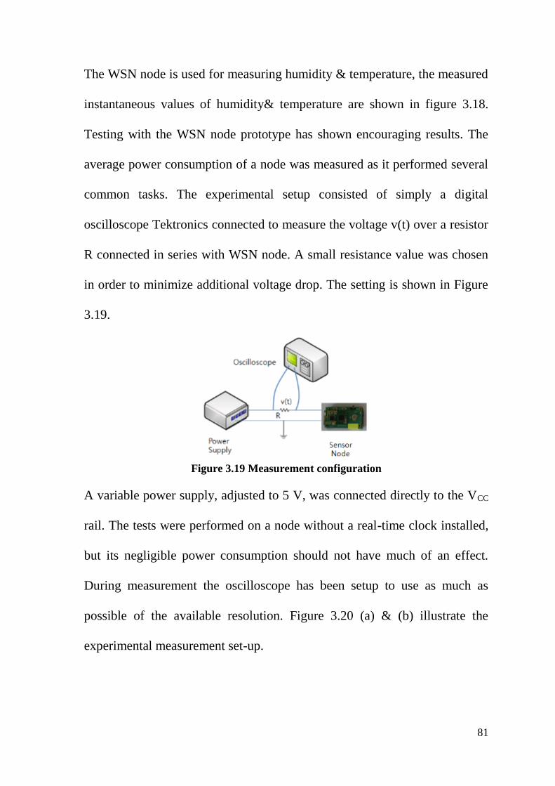
81
The WSN node is used for measuring humidity & temperature, the measured
instantaneous values of humidity& temperature are shown in figure 3.18.
Testing with the WSN node prototype has shown encouraging results. The
average power consumption of a node was measured as it performed several
common tasks. The experimental setup consisted of simply a digital
oscilloscope Tektronics connected to measure the voltage v(t) over a resistor
R connected in series with WSN node. A small resistance value was chosen
in order to minimize additional voltage drop. The setting is shown in Figure
3.19.
Figure 3.19 Measurement configuration
A variable power supply, adjusted to 5 V, was connected directly to the VCC
rail. The tests were performed on a node without a real-time clock installed,
but its negligible power consumption should not have much of an effect.
During measurement the oscilloscope has been setup to use as much as
possible of the available resolution. Figure 3.20 (a) & (b) illustrate the
experimental measurement set-up.

82
Figure 3.20(a) Measurement set-up
Figure 3.20(b) Measurement set-up

83
Several assembly language program routines were written to test various
modes of WSN node. The WSN node modes are sleep, receive, send and
measure. Sleep mode is when the node has nothing to do and therefore the
components are in their power save mode. Receive mode is when the node
listens and receives sensed data. Send mode is when the node transmits data
and measure mode is when the node measures the humidity and temperature.
The first, sleep mode, put the microcontroller and radio transceiver into their
low-power sleep modes. Second, the current consumption of measuring
mode was tested. The microcontroller enables ADC and samples data from
it. Next, receive mode was tested. In this mode, the microcontroller put the
radio transceiver into it’s receive mode. Finally, transmission mode was
tested. To transmit, the microcontroller placed the radio transceiver into
OOK transmit mode, then enabled its onboard serial port and transmitted
DC-balanced data.
3.11 Experimental Results
The nodes shall consume less power. Table 3.5 gives the calculated current
consumption per circuit for all the modes. Typical current ratings of various
components were taken from their standard datasheets.

84
Table 3.5 Power Consumption per Circuit
Mode Transceiver
mA
ADC
mA
MCU
mA
Sensor 1
mA
Sensor 2
mA
Total
mA
Sleep 0.160 0.001 0.050 0.002 0.001 0.214
Receive 17.000 0.001 25.000 0.002 0.001 42.004
Send 21.500 0.001 25.000 0.002 0.001 46.504
Measure 0.160 3.000 0.050 0.500 0.060 3.770
The nodes must be able to live at least a couple of months since it will be
impractical to change batteries all the time. To be able to fulfill this
requirement, the nodes cannot constantly listen for communications. To
transmit data the node must know when the receiving node is listening.
Therefore all nodes follow a schedule that defines when each node listens,
sleep or transmit data. The schedule will be based on a 24 bit timer that is
divided into 3 parts. The first part is called Sensor Schedule and is used to
schedule sensor measurements. Next part is called Transceiver schedule and
is used to schedule the transmitting and receiving data from the nodes. Each
step in the Transceiver schedule will be dedicated to a specific node and
these slots will be called time slots. Node 1 listens on time slot 1 and node 2
listens on time slot 2 and so on. The lowest part is used to determine the
position in the current time slot and is called Transceiver schedule Position
Counter. The slots, sensor schedule, transceiver schedule and transceiver
position counter are each 8 bits long because of the 8bit processor
architecture. There are 256 time slots because the Transceiver schedule

85
Position Counter is one byte. 16 of those time slots are needed by transceiver
for transmission or reception of data. This will give a maximum of 240 time
slots that can be used by nodes and since every node needs at least one time
slot there can at most be 240 nodes including the base station. The
Transceiver schedule is clocked with 4096 Hz so that the whole time cycle
becomes (256*256)/4096Hz which comes out to be 16 seconds. Since there
are 256 time slots we divide the time with 256 to get the time for each time
slot i.e. 256/4096Hz equals to 0.0625 seconds. The bit rate is specified as 20
kbit per second and that will give 20 kbits/second * (16seconds / 256slots)
which comes out to be 1250 bits/slot.
The bit per slot rate will give (1250bits/slots) / (8x8bytes/package) which
equals to 19.5 packets/slot. The calculations show that 19 packets can be
transmitted per time slot. Since each packet needs to be acknowledged by the
receiver there will only be 8 data packets and 8 acknowledge packets per
time slot. In Table 3.6 the average current is calculated from the usage
percentage and current consumption of each mode.
Since WSN node transmits one data packet every time cycle and every
packet takes 1/16 of a time slot gives the Transmit time (%) as 2/(256 x 16)
which becomes 0.048 %. The node listen one slot per time cycle which gives
Receive time (%) as 1/256 which becomes 0.4%. The measurement takes
200ms and the time cycle is 16s long. This gives Measure time (%) as

86
0.2/16 which is equal to 1.25% and the rest of the time the node will be in
sleep mode which is given by 100 - 0.4 - 0.048 - 1.25 that comes out to be
98.302%. for each mode usage percentage is then multiplied with its current
and the sum of all currents gives average current consumption.
Table 3.6 Calculated Current Consumption
Mode % of Time mA mA
Sleep 98.302 0.214 0.210
Receive 0.4 42.004 0.168
Send 0.048 46.504 0.022
Measure 1.25 3.770 0.047
Total 100.0 0.447
The actual current consumption of the node was also measured and recorded.
Since it is not possible to measure the current consumption of each
component, therefore only the total consumption per mode is presented in
Table 3.7.
Table 3.8 Measured Current Consumption
Mode % of Time mA mA
Sleep 98.302 0.279 .274
Receive 0.4 42.29 .169
Send 0.048 46.817 .022
Measure 1.25 3.98 .049
Total 100.0 .514
A node equipped with 2 AA batteries with capacity 3000mAh having an
average current consumption of 0.514 mA will stay alive for about
3000mAh / 0.514 that is equal to 5836 hours which is equivalent to 243 days
(8 months approx).

87
The measured current values matched closely with calculated current
consumptions. The sleep mode currents are negligible, and will allow
operation from AA size lithium battery for months. This testing verified that
this design had the functionality to be a WSN node for agricultural
application.
3.12 Debugging Circuit
For optimizing power consumption and size of the board, limited debugging
capabilities are built onto the WSN node circuit board. Various test points
were created on circuit board and the voltages were recorded at each point
for future reference and debugging. The transceiver must be tested by
programming the microcontroller with a test program and monitoring data
received on the other node for this a test program was created and stored in
program memory of microcontroller. A reset switch is added to reset the
system.
3.13 Summary of the chapter
A pair of WSN node was constructed, one is kept at the field and other one is
kept at operating room. The Node is effectively monitoring and transmitting
the change in humidity & temperature. A step-by-step approach in designing
the microcontroller based system for monitoring the essential parameters for
plant growth, i.e. humidity & temperature has been followed. The results
obtained from the measurement have shown that the system performance is

88
quite reliable and accurate. The system has successfully overcome quite a
few shortcomings of the existing systems by reducing the power
consumption, maintenance and complexity, at the same time providing a
flexible and precise form of maintaining the environment. The continuously
decreasing costs of hardware and software, the wider acceptance of
electronic systems in agriculture, and an emerging agricultural control
system industry in several areas of agricultural production, will result in
reliable control systems that will address several aspects of quality and
quantity of production. In future more developments will be made as cost
effective and more reliable WSN nodes will be made available for use in
agricultural production.

89
CHAPTER 4:
System Architecture for
Wireless Sensor Node
System architecture of Wireless Sensor
Networks Node was developed and these are
discussed in the chapter.

90
CHAPTER 4: System Architecture for Wireless Sensor
Node
4.1 Overview
This chapter deals with the design of architecture of the processing unit of
WSN node. A custom designed processing unit is a programmable unit
optimized for WSN node agricultural application and is the heart of WSN
node. A custom designed processing unit will have an event processor as
main computational element. Use of custom designed processing unit in a
WSN node has the advantage of flexibility along with achieving good
performance, high reliability and low power consumption over conventional
processing units [141-144].
4.2 Processing Unit
A basic processing unit consists of a controller and a datapath as shown in
figure 4.1 [145-146].

91
Figure 4.1 Control unit and the datapath of processing unit.
The datapath stores and manipulates system’s data. The data in the case of
WSN node is the data acquired by the sensors of node after measuring the
ambient conditions [147-149]. The data is stored, processed and compressed
for transmission. The controller is capable of moving data through datapath.
The combinational and sequential logic design techniques are applied to
build a controller and data path for a custom designed event processor for
WSN Node. Such custom designed event processor results in several
benefits in terms of faster performance, smaller size lower power
consumption [150-152].
Custom designed processing unit consists of datapath for storing and
manipulating data and a controller block. The controller block consists of
two parts: an event detector and a sub-controller. The event detector
indicates to the sub-controller when there is significant change in the
measured quantity (event) [153]. In an event-based system, the occurrence of

92
an event, rather than the time, is what decides when a sample should be
taken. The nature of the event can be defined as the value when a measured
signal crosses a certain limit or threshold [154].
The event-based processor has allowed a considerable decrease in the
number of changes in the control action and made possible the compromise
between quantity of transmission and performance. Event-based processor
for WSN node will not only reduce post processing latency but will also
reduce the overall power consumption in a wireless sensor network node.
This is achieved by reducing the amount of data transmitted by the post
processing unit which shares a large amount of total power consumed by a
WSN node there by resulting in a low power WSN node. WSN node using
customizable low power processor can find a wide application in different
areas, especially where it is needed to monitor and save bulk data for
different agricultural and non-agricultural practices [155-163]. Custom
designed processor can be designed at various abstraction levels. The lowest
level is the transistor level in which discrete transistors are connected to form
the circuit. The next level up is the gate level in this level, logic gates are
used to build the circuit. In gate level, design the circuit is created using
either a truth table or a Boolean equation. Finally, at the highest level is the
behavioral level [164]. In behavioral modelling the circuit is designed by
describing the behavior or operation of the circuit using a hardware

93
description language. This is very similar to writing a computer program
using a programming language [165-167].
A Custom Designed event processor is implemented by VHDL code. Design
verification was done at the pre-synthesis, post-synthesis and post-layout
levels using Active HDL6.3 sp3 [168]. The Custom Designed event
processor was synthesized using Synplify Pro. Final layout was imported
into Xilinx ISE to perform design rule check.
4.3 Architecture Description
To fulfill design goals, the basic functionality of a general-purpose
processing unit is replaced with a modularized, custom designed event-
driven system [169-172]. There are two distinct divisions within the system.
We refer some of the components as slave components and some as master
components. The system bus has three divisions – data, interrupt, and power
control. The central arbitration system resolves the interrupt requests in case
of the multiple interrupt request raised by the slave components compete for
the interrupt bus. The master components read, decode and control
execution of the instructions. In this process the slave components follow
the read and write instructions issued from the master components on the
data bus for smooth execution of the decoded instructions [173].
4.3.1 Event-Driven System
An event-driven system is the one in which all of the master components are

94
involved with event handling, and the slaves assist the master components in
their tasks and slave components also signal the occurrence of events to the
master components. All external events, such as the beginning of data
transmission, are indicated as interrupts by an appropriate slave component.
The slave components also raise interrupts request for their internal events,
such as completion of an assigned task. Master components do not
differentiate between external and internal events. Also, since the
occurrence of all events is signaled by interrupts, the terms event and
interrupt are used interchangeably. The system remains in idle mode until
one of the slaves component signals the presence of an event and raises an
interrupt request, and when all outstanding interrupts have been processed,
the system again returns to its idle mode. Since all the system does is
respond to an interrupt only when an event occurs, there is no software
overhead for interrupt handling [174].
4.3.2 Improved Performance and Power
In the proposed design the event detector calls upon main processing section
to perform a task only if the event of interest i.e. significant change in the
measured quantity occurs. Specific tasks that are considered common to a
wide variety of application are offloaded to hardware components like
comparator, which can be more power and cycle efficient than the main
processor. Hence, the custom designed processor can usually be powered
down by gating the supply voltage [175]. This reduces active power as well

95
as leakage power, in a digital system leakage power is a very significant
source of power consumption for low duty cycle operation.
4.3.3 Scheduling events
Within an application all immediate interrupt handling is offloaded to the
event detector block while the other processing blocks are powered down.
The event detector is a simple state machine that can be programmed to
handle an interrupt by transferring data blocks between the slave devices
and setting up control information for these devices to complete their tasks.
The event detector has the option to be programmed to wake up the other
processing blocks if the desired function for processing the current interrupt
is not possible by slave components. The event detector can be considered
as an intelligent programmable interrupt controller (PIC) [176-178].
Interrupt service routines (ISRs) are processed at two different stages: first
all the ISRs are handled at the event detector stage and secondly they are
passed for handling at the processing blocks level. ISRs at both the stages
whether the event detector stage or the processing blocks stage are stored as
vector table in the main memory. The main memory acts as a program and
data memory for handling ISRs. Events can be classified as a regular event
and an irregular event. A regular event is one that can be processed wholly
by the event detector and the slave components. An irregular event is one
that requires the other processing blocks like ALU etc. One of the tasks
involved in mapping an application to the system is to determine the

96
partitioning of events into regular and irregular events. Whether an event is
regular or not is determined is dependent on the capabilities of event
detector and processing unit for example if a particular event can be handled
totally by event detector and its supporting components then it is a regular
event [179-181]. For a general WSN application, events like sensing,
collecting sample data, transmitting and forwarding samples would be
considered as regular events while processing or compressing the data
would be classified as irregular.
4.3.4 Event handling process
The system is designed to process one interrupt request at a given instance
of time. Therefore if the slave devices have more than one outstanding
interrupt they may continue to raise interrupt request to interrupt bus. Since
the system can process only one interrupt at a time therefore eventually all
the interrupts generated by the other events while the current interrupt is
processed will be dropped i.e. events generated during this period will be
dropped [182]. Outstanding events cannot request interrupt handling unit to
relinquish the bus either from the processing blocks or the event detector.
The system bus, the processing blocks, and the event detector are all non-
pipelined. All of these simplifications give rise to a light-weight system that
is well suited to handle monitoring applications while consuming very little
power.
4.3.5 Modularity

97
The entire slave devices are attached to the system bus and are memory
mapped. Both control and data are communicated to and from the slaves by
simply reading from and writing to appropriate addresses in the memory.
This memory mapped interface allows the system design to be extremely
modular and new components and hence new functionality can be added on
to the system bus without modification of the event detector or the
processing blocks [183-184].
4.3.6 Power Management
Is based on Computational Requirements since the master components are
triggered by interrupts, the ISRs for each interrupt can configure the system
according to its computational requirements for handling the interrupt. To
sufficiently curb leakage power, special instructions within the event
detector are used to gate the supply voltages of system components. Note
that the system does not infer the resource usage for an event; rather, the
ISR programmer selects the components to turn on depending on the needs
of the application. Individual power enable lines are required for each
component under direct control. Vdd-gating and power down
implementations will vary depending on the circuit-level design of the
individual slave components [185]. Such power control may not only be
exercised over the slave components, but also over segments within the
main memory that contain temporary data, such as application scratch space.
The event-driven programmable resource usage is one of the most

98
significant innovations of the system design. It allows configuration of
system power consumption with very little logic over- head, as opposed to a
technique that attempts to infer resource usage. Also, it allows the addition
of several specific components to the system as slaves that can be used in
varying combinations to provide the functionality required by an
application. Any component unused in an application can be turned off (i.e.,
supply voltage gated) and is nearly invisible during the entire lifetime of the
application. Therefore, the system can satisfy the general-purpose
requirements of applications by providing a broad range of slave
components, enabling an on-demand functionality that imposes negligible
overhead when a component is not required [186].
4.4 System Components
Details of other system components are described in following section:
System Bus: As discussed earlier, the system bus consists of the data bus,
the address bus, and control bus. The control bus has generates control
signals indicating read and write operations. In current implementation the
address bus has 16 lines, the data bus has 8 lines, and there is one control
signal each for read and write operations. The address space for memory-
mapped architecture is therefore 64K. The address and control lines can be
controlled only by the event detector and the processing blocks in mutual
exclusion as determined by the bus arbiter, which is just a multiplexer. The

99
data lines are driven by the controller that determines that whether the
current request lies in its address range, and are demultiplexed to the
initiator of the request, i.e., the event detector or the processing blocks.
The interrupt bus has 6 address lines and control signals for arbitrating the
writing of interrupts by slaves. The system is therefore capable of handling
64 interrupts. The event detector has control signals in the interrupt bus to
indicate when it has read the current interrupt address.
The handshake is relevant only when a component is turned on, to determine
the time when the component can be used.
4.4.1 Processing blocks:
The processing blocks is used to handle irregular events, as discussed
in previous sections, such as system initialization and reprogramming.
The processing blocks is a simple non pipelined processing blocks. It
implements an 8-bit Instruction Set Architecture (ISA). The system uses
available computational cores with necessary modifications for low-power
features required for the system.
4.4.2 Event Detector:
The event detector is essentially a programmable state machine designed to
perform the repetitive task of interrupt handling. Figure 4.2 illustrates a
simplified version of the actual state machine within the event processor.
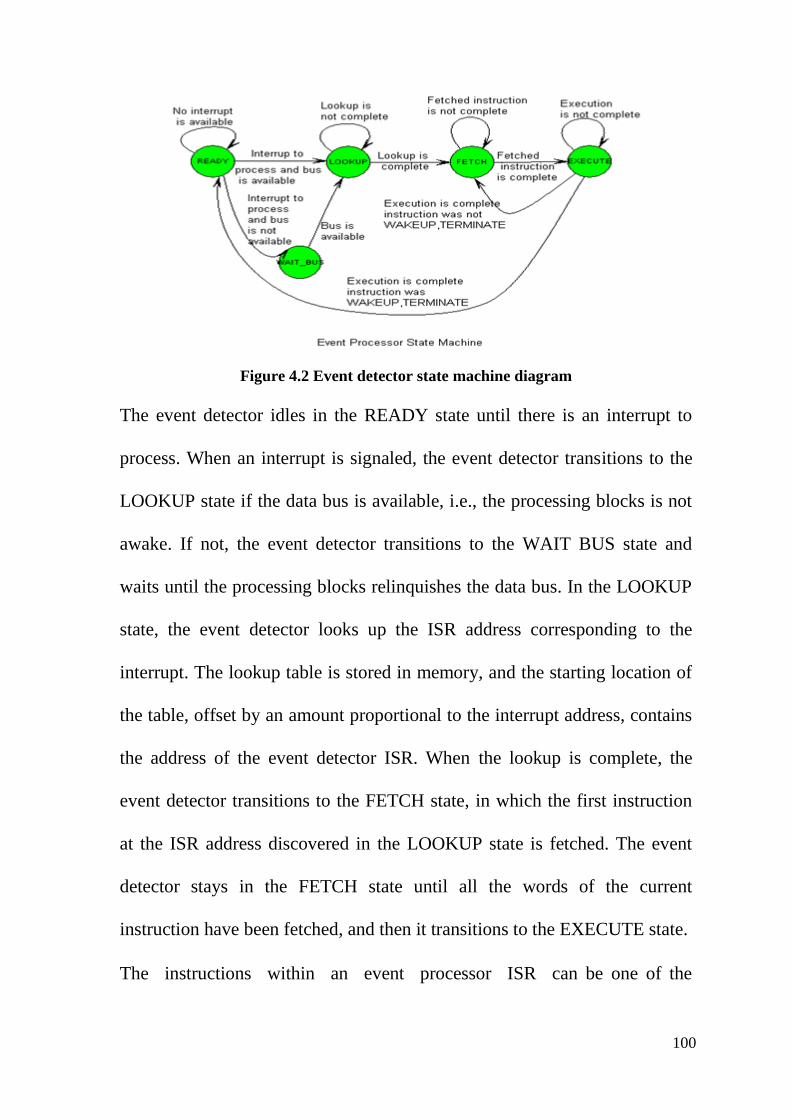
100
Figure 4.2 Event detector state machine diagram
The event detector idles in the READY state until there is an interrupt to
process. When an interrupt is signaled, the event detector transitions to the
LOOKUP state if the data bus is available, i.e., the processing blocks is not
awake. If not, the event detector transitions to the WAIT BUS state and
waits until the processing blocks relinquishes the data bus. In the LOOKUP
state, the event detector looks up the ISR address corresponding to the
interrupt. The lookup table is stored in memory, and the starting location of
the table, offset by an amount proportional to the interrupt address, contains
the address of the event detector ISR. When the lookup is complete, the
event detector transitions to the FETCH state, in which the first instruction
at the ISR address discovered in the LOOKUP state is fetched. The event
detector stays in the FETCH state until all the words of the current
instruction have been fetched, and then it transitions to the EXECUTE state.
The instructions within an event processor ISR can be one of the

101
following – SWITCHON, SWITCHOFF, READ, WRITE, WRITEI,
TRANSFER, TERMINATE, or WAKEUP. Table 4.1 provides the
description of all the instructions. The event detector has one general
purpose register used for storing temporary data. The op- codes are each 3
bits and the instructions vary in the number of words they span.
Table 4.1: Instruction Set with description
Instruction Size Description
SWITCH ON One Byte Turn on a component & wait for acknowledgement
that the component is ready to proceed.
SWITCH OFF One Byte Turn off a component.
READ Three Bytes Read a location in address space & store to the
register.
WRITE Three Bytes Write a location in address space & store to the
register.
WRITEI Three Bytes Write an immediate value to a location in address
space.
TRANSFER Five Bytes Transfer a block of data within the address space.
TERMINATE One Byte Terminate the ISR without waking up the processing
blocks.
WAKEUP Two Bytes Terminate the ISR & wake up the processing blocks at
a processing blocks ISR address.
The EXECUTE state is maintained till the EXECUTE instruction has been
completely executed, e.g., the complete transfer has been completed for a
TRANSFER instruction. A component is completely powered on receiving
SWITCHON instruction. If the instruction is not a WAKEUP or
TERMINATES instruction, the event detector returns to the FETCH state
and fetches the next instruction in the ISR for execution. For WAKEUP or

102
TERMINATE instructions, the event detector returns to the READY state
and waits for the next interrupt request to occur. Regular events such as
table lookup and check-sum calculations can be implemented using
hardware thereby reducing programming overhead.
Currently, the event processor interface has two memory blocks for each
event as well as memory-mapped control words. Data is transferred to the
event processor from sensor devices and once the event has been prepared
the event processor raises an interrupt request and the event are sent to the
transceiver. All incoming events are transferred from the transceiver to the
event processor. If the event is a regular event, the event processor looks up
whether the event should be forwarded. If the event is an irregular event,
then an interrupt request is raised and the event detector wakes up the
processing blocks.
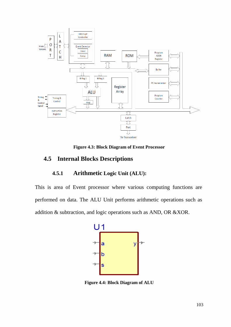
103
Figure 4.3: Block Diagram of Event Processor
4.5 Internal Blocks Descriptions
4.5.1 Arithmetic Logic Unit (ALU):
This is area of Event processor where various computing functions are
performed on data. The ALU Unit performs arithmetic operations such as
addition & subtraction, and logic operations such as AND, OR &XOR.
Figure 4.4: Block Diagram of ALU
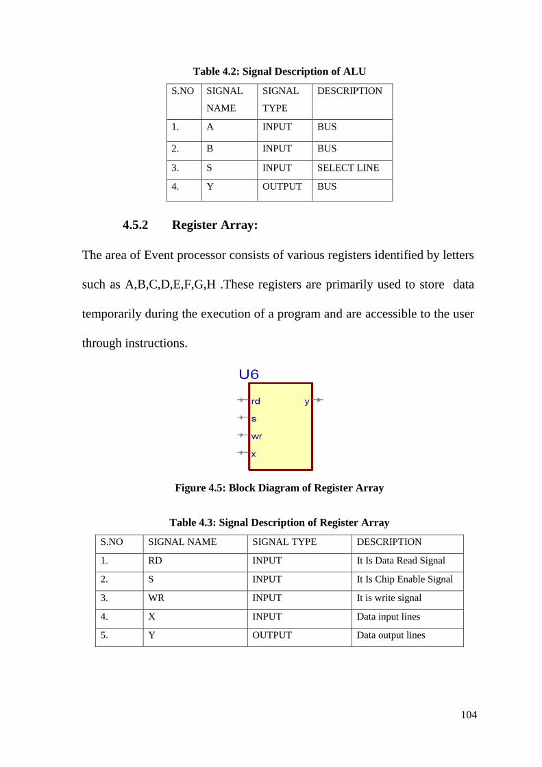
104
Table 4.2: Signal Description of ALU
S.NO SIGNAL
NAME
SIGNAL
TYPE
DESCRIPTION
1. A INPUT BUS
2. B INPUT BUS
3. S INPUT SELECT LINE
4. Y OUTPUT BUS
4.5.2 Register Array:
The area of Event processor consists of various registers identified by letters
such as A,B,C,D,E,F,G,H .These registers are primarily used to store data
temporarily during the execution of a program and are accessible to the user
through instructions.
Figure 4.5: Block Diagram of Register Array
Table 4.3: Signal Description of Register Array
S.NO SIGNAL NAME SIGNAL TYPE DESCRIPTION
1. RD INPUT It Is Data Read Signal
2. S INPUT It Is Chip Enable Signal
3. WR INPUT It is write signal
4. X INPUT Data input lines
5. Y OUTPUT Data output lines
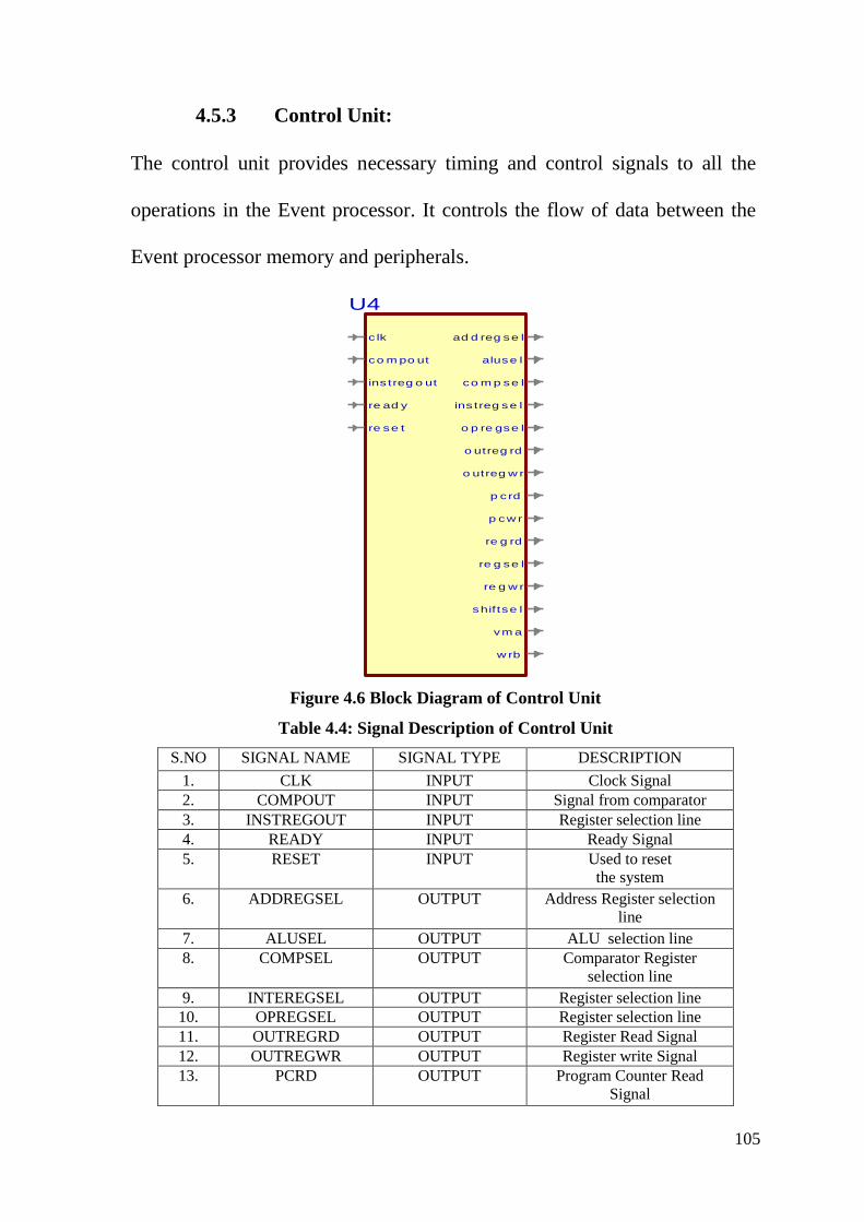
105
4.5.3 Control Unit:
The control unit provides necessary timing and control signals to all the
operations in the Event processor. It controls the flow of data between the
Event processor memory and peripherals.
c lk ad d reg se l
co m po ut aluse l
ins treg o ut co m p se l
re ad y ins treg se l
re se t o p re gse l
o utreg rd
o utreg w r
p crd
p cw r
re g rd
re g se l
re g w r
shif tse l
vm a
w rb
U4
control
Figure 4.6 Block Diagram of Control Unit
Table 4.4: Signal Description of Control Unit
S.NO SIGNAL NAME SIGNAL TYPE DESCRIPTION
1. CLK INPUT Clock Signal
2. COMPOUT INPUT Signal from comparator
3. INSTREGOUT INPUT Register selection line
4. READY INPUT Ready Signal
5. RESET INPUT Used to reset
the system
6. ADDREGSEL OUTPUT Address Register selection
line
7. ALUSEL OUTPUT ALU selection line
8. COMPSEL OUTPUT Comparator Register
selection line
9. INTEREGSEL OUTPUT Register selection line
10. OPREGSEL OUTPUT Register selection line
11. OUTREGRD OUTPUT Register Read Signal
12. OUTREGWR OUTPUT Register write Signal
13. PCRD OUTPUT Program Counter Read
Signal
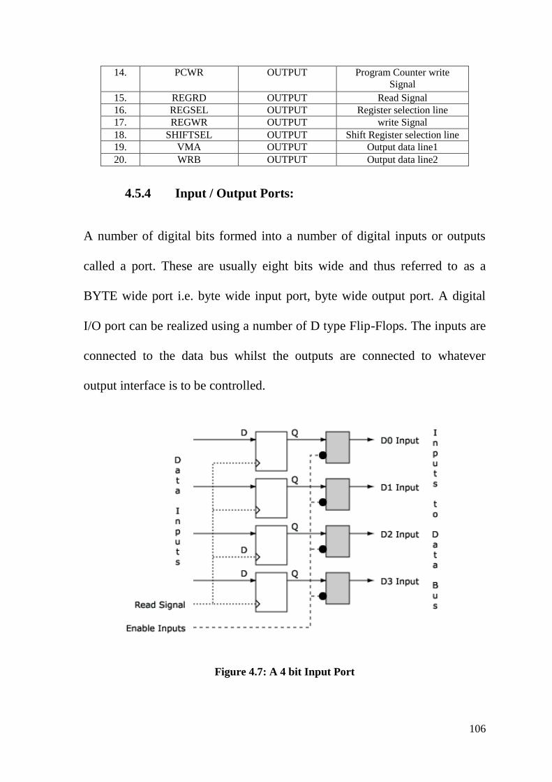
106
14. PCWR OUTPUT Program Counter write
Signal
15. REGRD OUTPUT Read Signal
16. REGSEL OUTPUT Register selection line
17. REGWR OUTPUT write Signal
18. SHIFTSEL OUTPUT Shift Register selection line
19. VMA OUTPUT Output data line1
20. WRB OUTPUT Output data line2
4.5.4 Input / Output Ports:
A number of digital bits formed into a number of digital inputs or outputs
called a port. These are usually eight bits wide and thus referred to as a
BYTE wide port i.e. byte wide input port, byte wide output port. A digital
I/O port can be realized using a number of D type Flip-Flops. The inputs are
connected to the data bus whilst the outputs are connected to whatever
output interface is to be controlled.
Figure 4.7: A 4 bit Input Port

107
The input port allows outside world inputs to be stored in the data latches so
they can be read by the event detector via the data bus. The data bus
connections must be via tri-state buffers so that the input port is only
connected to the data bus when the input port is selected. This is achieved by
connecting a chip select signal to the enable input signal line.
Figure 4.8: A 4 bit Output Port
4.5.5 Bi Register
Figure 4.9: Block Diagram of Bi Register
a y
s
U2
bireg
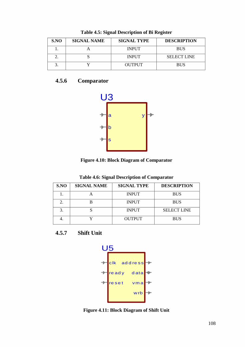
108
Table 4.5: Signal Description of Bi Register
S.NO SIGNAL NAME SIGNAL TYPE DESCRIPTION
1. A INPUT BUS
2. S INPUT SELECT LINE
3. Y OUTPUT BUS
4.5.6 Comparator
a y
b
s
U3
comp
Figure 4.10: Block Diagram of Comparator
Table 4.6: Signal Description of Comparator
S.NO SIGNAL NAME SIGNAL TYPE DESCRIPTION
1. A INPUT BUS
2. B INPUT BUS
3. S INPUT SELECT LINE
4. Y OUTPUT BUS
4.5.7 Shift Unit
c lk ad d re ss
re ad y d ata
re se t vm a
w rb
U5
mp
Figure 4.11: Block Diagram of Shift Unit

109
Table 4.7: Signal Description of Shift Unit
S.NO SIGNAL NAME SIGNAL TYPE DESCRIPTION
1. CLK INPUT Clock Signal
2. READY INPUT Ready Signal
3. RESET INPUT Used to reset
the system
4. ADDRESS OUTPUT Address Lines
5. DATA OUTPUT Data output lines
6. VMA OUTPUT Output data line1
7. WRB OUTPUT Output data line2
4.5.8 Latch
A latch is a basic element of memory. To write or store a bit in latch, we
need an input data bit (INP) and an enable signal (EN), as shown in figure.
In this latch, the stored bit is always available on the output line (OUTP).
C L K
O U T P(7 :0 )IN P (7:0 )
U3
Latch
Figure 4.12: Block Diagram of Latch
Table 4.8: Signal Description of Latch
S.NO SIGNAL NAME SIGNAL TYPE DESCRIPTION
1. INP INPUT Data input lines
2. CLK INPUT It Is clock Signal
3. OUTP OUTPUT Data output lines
4.6 Memory Unit

110
4.6.1 Read Only Memory (ROM)
This is memory that can only be read, the data being stored in the memory
device during its manufacture.
Erasable Programmable Read Only Memory (EPROM). This is similar
to ROM type memory but the user can program it. The contents of the
memory can be erased from the memory by exposing the memory chip to
ultraviolet radiation for a short period of time. It can therefore be used many
times over.
Electrically Erasable Programmable Read Only Memory (EEPROM).
Similar to EPROM but has part or all of the memory contents erased by the
Customizable logic controller.
Both ROM and EPROM memory are used to hold the program code of a
microprocessor used in an embedded system, i.e. a Customizable logic
controller used in an application where the program code is always the same
and is designed to execute every time the system is switched on. Most
development work is done using EPROM or EEPROM type memory, ROM
memory being used in the final production version (when all the program
code has been fully tested).

111
A D D RE S S(1 9:0 ) Q (1 5:0 )
O E
U1
rom
Figure 4.13 Block Diagram of ROM
Table 4.9 Signal Description of ROM
S.NO SIGNAL NAME SIGNAL TYPE DESCRIPTION
1. OE INPUT
It Is Chip Enable
Signal
2. ADDRESS INPUT
Address Lines
3. Q OUTPUT
Bidirectional data bus
4.6.2 Random Access Memory (RAM)
Customizable logic controller systems need memory that can be both read
from and written to. RAM memory is used to store dynamic data (that will
change during the operation of the program).
So a typical Customizable logic controller system will contain both ROM
(could be EPROM, EEPROM, or ROM) to store the program code, and
RAM to store dynamic data.
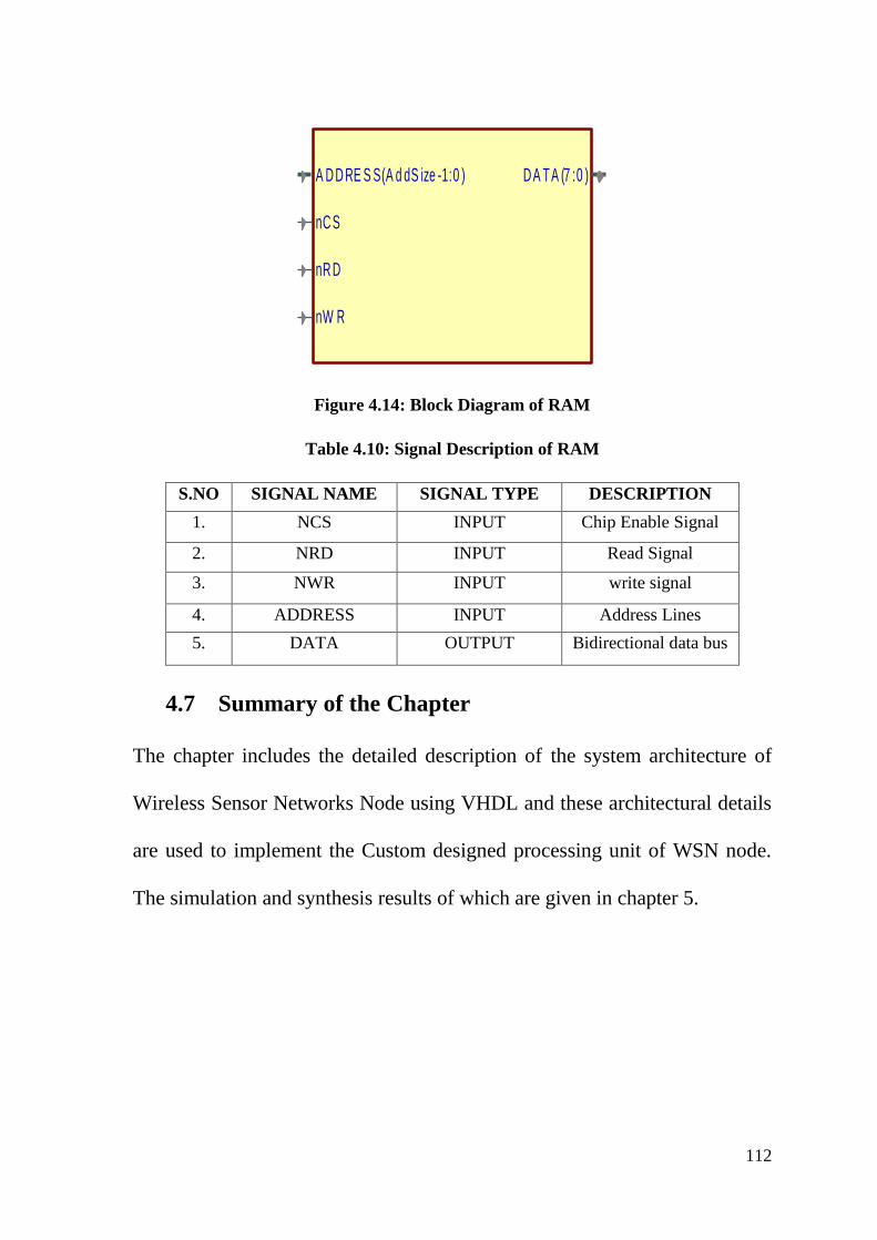
112
D A TA (7 :0 )
nC S
nR D
nW R
A D D RE S S(A d dS ize -1:0 )
U4
ram
Figure 4.14: Block Diagram of RAM
Table 4.10: Signal Description of RAM
S.NO SIGNAL NAME SIGNAL TYPE DESCRIPTION
1. NCS INPUT Chip Enable Signal
2. NRD INPUT Read Signal
3. NWR INPUT write signal
4. ADDRESS INPUT Address Lines
5. DATA OUTPUT Bidirectional data bus
4.7 Summary of the Chapter
The chapter includes the detailed description of the system architecture of
Wireless Sensor Networks Node using VHDL and these architectural details
are used to implement the Custom designed processing unit of WSN node.
The simulation and synthesis results of which are given in chapter 5.

113
CHAPTER 5:
Implementation
and Result
Implementation of Custom Designed
Processing Unit and Results
The chapter covers the implementation
methodology for custom designed processing
unit, its evaluation and calculation of power
consumption and enumeration of results.

114
CHAPTER 5: Implementation & Result
5.1 Introduction
As discussed in chapter 1 the central component of a WSN node is
processing unit. The processing unit is typically implemented by a general
purpose microprocessor or a microcontroller, which integrates a processor
core with program and data memories, timers, configurable I/O ports,
Analog-to-Digital Converter (ADC) and other peripherals. The major
drawback of such processing unit is that it contains several components that
are not required in a WSN node. These undesired components in general
purpose processors consume power [187, 188]. To address this issue a
custom designed processing unit is proposed as solution. The aim of this
chapter was to implement a custom designed processing unit for WSN node.
Custom designed processing unit designed for use in low-power wireless
sensor-network nodes will not only reduce post processing latency but it will
also reduce the overall power consumption in a wireless sensor network

115
node. This is achieved by customizing the components in processing unit
which shares a large amount of total power consumed by a WSN node [189].
5.2 Implementation of Processing Unit-Custom Designed
Event Processor
Custom designed processing unit consists of an Event processor. Event
processor of the custom designed processing unit will help WSN node to
respond only to the occurrence of significant change in the value of the
quantity being measured (event). Custom designed processing unit is
implemented by complete process of simulation, synthesis of a VHDL model
[190-194], performing placement, routing, and finally simulating the final
netlist. Components of custom designed processing unit are broken down
into common substructures such as incrementers, comparators, buffers, etc.,
for implementation. The power consumption is estimated for all of these
components by simulating netlists synthesized for these sub-structures and
combining the results [195].
The implementation of various components of custom designed processing
unit using Active HDL-8 [196], Synplify Pro [197], Xilinx ISE [198] is
given in following section:

116
5.2.1 ALU
library event_processor_f... use event_processor...library ieee; use ieee.std_logic_1... use ieee.std_logic_u...
Design Unit Headerprocess (a,b,s) begin case s is when add y <= a + when sub y <= a - b when inc... y <= a + when dec
a
b
s
y
Figure 5.1: Logical Diagram of ALU
The above shown logical diagram is of ALU that was designed using active
HDL 8.1.This ALU has a ‘a’& ‘b’ 16 bit input data line, a select line ‘s’ to
select the function of ALU. At the output it has a 16 bit output data line
namely as ‘y’.

117
[3]
[3]
[3]
[3]
[3]
[3]
[3]
[3]
[3]
[3]
[3]
[3]
[3]
[3]
[3]
[3]
un1_a[15:0]
aluproc.c_2[15:0]
aluproc.c_3[15:0]
aluproc.c_4[15:0]
un1_sel_1
aluproc.un1_sel
aluproc.c29
aluproc.c30
aluproc.c31
aluproc.c32
aluproc.c33
aluproc.c34
aluproc.c35
aluproc.c37
aluproc.un1_sel_1 un1_c37
un9_c[1:16]
+
un16_c[1:16]
+
aluproc.c_7[15:0]
+
un1_a_1[15:0]
+
c[15:0]
e
d
e
d
e
d
e
d
e
d
e
d
e
d
e
d
e
d
[15:0][15:0]
[15:0][15:0]
[15:0]
[15:0][15:0]
[15:0]
[15:0][15:0]
[15:0]
[0]
[1]
[2]
[1]
[2]
[0]
[1]
[2]
[3]
[0]
[1]
[2]
[3]
[0]
[1]
[2]
[3]
[0]
[1]
[2]
[3]
[0]
[1]
[2]
[3]
[0]
[1]
[2]
[3]
[0]
[1]
[2]
[3]
[0]
[1]
[2]
[3]
[3]
[15:0]
[1:16]
[15:0]
[15:0]
[1:16]
1
[15:0]
[15:0][15:0]
1
[15:0]
[15:0]
[15:0]
[15:0]
[15:0]
[15:0]
[15:0][1:16]
[15:0]
[1:16]
[15:0]
0*16
c[15:0][15:0]
sel[3:0][3:0]
b[15:0][15:0]
a[15:0][15:0]
Figure 5.2: RTL View of ALU

118
Figure 5.3: Snap Shot of RTL View of ALU (using Synplicity Pro)
The figure 5.2-5.3 shows the RTL schematic of the ALU (top) generated
from Synplify pro synthesis tool.
Figure 5.4: Result Verification Waveform of ALU
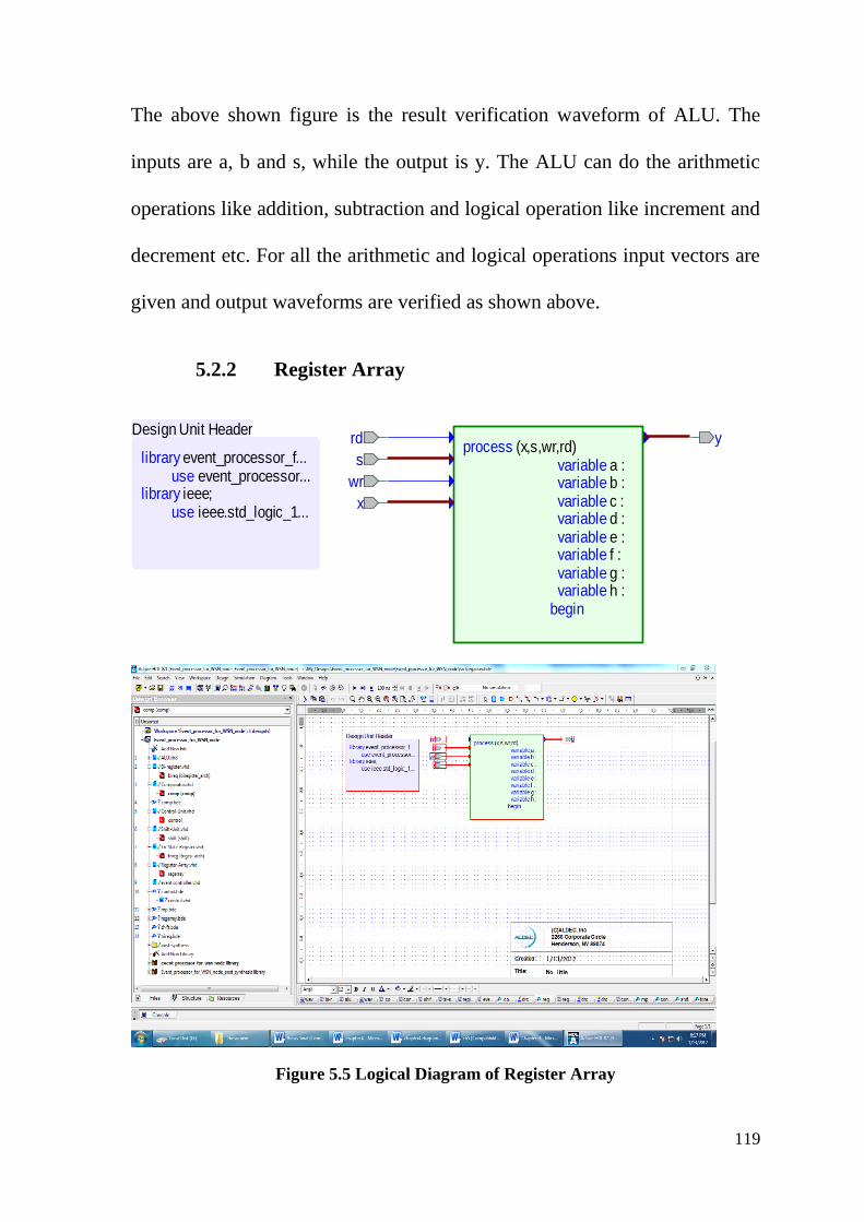
119
The above shown figure is the result verification waveform of ALU. The
inputs are a, b and s, while the output is y. The ALU can do the arithmetic
operations like addition, subtraction and logical operation like increment and
decrement etc. For all the arithmetic and logical operations input vectors are
given and output waveforms are verified as shown above.
5.2.2 Register Array
library event_processor_f... use event_processor...library ieee; use ieee.std_logic_1...
Design Unit Headerprocess (x,s,wr,rd) variable a : variable b : variable c : variable d : variable e : variable f : variable g : variable h : begin
rd
s
wr
x
y
Figure 5.5 Logical Diagram of Register Array

120
The above shown logical diagram is of register array that was designed using
active HDL 8.1.This register array has a ‘clk’ input signal, a select line ‘sel’,
an enable signal ‘en’ and 16 bit input data line ‘data’. At the output it has a
16 bit output data line namely as ‘q’.
un18_wr
un2_rd
un4_wr
un6_wr
un8_wr
un10_wr
un12_wr
un14_wr
un16_wr
un1_s_4
un1_s_5
un1_s_6
un1_s_7
un1_s_8
un1_s_9
un1_s_10
un1_wr_1
un1_wr_2
un1_wr_3
un1_wr_4
un1_wr_5
un1_wr_6
un1_wr_7
un1_wr_8
lat
h[15:0]
lat
a[15:0]
lat
b[15:0]
lat
c[15:0]
lat
d[15:0]
lat
e[15:0]
lat
f[15:0]
lat
g[15:0]
y_9[15:0]
e
d
e
d
e
d
e
d
e
d
e
d
e
d
e
d
lat
y[15:0]
[0]
[1]
[2]
[0]
[1]
[2]
[0]
[1]
[2]
[1]
[0]
[2]
[0]
[1]
[2]
[2]
[0]
[1]
[0]
[2]
[1]
[1]
[2]
[0]
[0]
[1]
[2]
[0]
[1]
[2]
[1]
[0]
[2]
[0]
[1]
[2]
[2]
[0]
[1]
[0]
[2]
[1]
[1]
[2]
[0]
[15:0]D[15:0] [15:0]
Q[15:0]C
[15:0]D[15:0] [15:0]
Q[15:0]C
[15:0]D[15:0] [15:0]
Q[15:0]C
[15:0]D[15:0] [15:0]
Q[15:0]C
[15:0]D[15:0] [15:0]
Q[15:0]C
[15:0]D[15:0] [15:0]
Q[15:0]C
[15:0]D[15:0] [15:0]
Q[15:0]C
[15:0]D[15:0] [15:0]
Q[15:0]C
[15:0]
[15:0]
[15:0]
[15:0][15:0]
[15:0]
[15:0]
[15:0]
[15:0]
[15:0]D[15:0] [15:0]
Q[15:0]C
y[15:0][15:0]
s[2:0][2:0]
wr
rd
x[15:0][15:0]
Figure 5.6: RTL View of Register Array

121
The figure 5.6 shows the RTL schematic of the register Array (top)
generated from Synplify pro synthesis tool.
Figure 5.7: Result Verification Waveform Register Array
The above shown figure is the result verification waveform of register array.
To verify the result, an input clock signal ‘clk’ is applied. To enable the
register array an enable signal ‘en’ has to be given. Now when the select
input is at ‘1’ and the data at the input lines is 0F0F, the output will be 0001.
5.2.3 Shift Unit

122
library event_processor_f... use event_processor...library ieee; use ieee.std_logic_1...
Design Unit Headerprocess (a,s) begin case s is when shl2 y <= a(14 when shr2 y <= '0'... when rol2 y <= a(14 when ror2
a
s
y
Figure 5.8: Logical Diagram of Shift Unit
The above shown logical diagram is of shift unit. This shift unit has a ‘a’
input signal, and a select line ‘sel’. At the output it has a 16 bit output data
line namely as ‘y’.

123
[0]
[15:1]
[14:0]
[15]
=0
[15:1]
[14:0]
=0
y[15:0]
e
d
e
d
e
d
e
d
e
d
[4]
[3]
[2][15:0]
[1]
[0]
[15:0]
y[15:0][15:0]
s[0:4][0:4]
a[15:0][15:0]
Figure 5.9: RTL View of Shift Unit
Figure 5.10: Snap Shot of RTL View of Shift Unit
The figure5.9-5.10 shows the RTL schematic of the Shift unit (top)
generated from Synplify pro synthesis tool.

124
Figure 5.11: Result Verification Waveform of Shift Unit
The above figure shows the result waveform of shift unit. To verify the
result, for the first 100 ns of time period when the select input is at ‘1’ and
the data at the input lines is F00F, the output will be E01E.
5.2.4 Tri-State Register
library event_processor_f... use event_processor...library ieee; use ieee.std_logic_1...
Design Unit Headerprocess (a,wr,rd) variable u : begin if (wr = '1') u := a; elsif (rd = '1' y <= u; else null; end if;
a
rd
wr
y

125
Figure 5.12: Logical Diagram of Tri State Register
The code and logical diagram of tri state register is shown in fig 5.12. This
register has a 16 bit input signal ‘a’, an enable signal ‘en’ and a clock signal
‘clk’. At the output it has a 16 bit output data line namely as ‘q’.
lat
u[15:0]
un2_rd
lat
y[15:0]
[15:0]D[15:0] [15:0]
Q[15:0]C
[15:0]D[15:0] [15:0]
Q[15:0]C
y[15:0][15:0]
wr
rd
a[15:0][15:0]
Figure 5.13: RTL View of Tri State Register

126
Figure 5.14: Snap Shot of RTL View of Tristate Register
The figure 5.13-5.14 shows the RTL schematic of the Tri State Register (top)
generated from Synplify pro synthesis tool, while fig 5.15 shows the
simulated waveform.
Figure 5.15: Result Verification Waveform of Tristate Register

127
5.2.5 Biregister
library event_processor_f... use event_processor...library ieee; use ieee.std_logic_1...
Design Unit Headerprocess (a,s) begin if (s = '1') t... y <= a; else null; end if; end process;
a
s
y
Figure 5.16: Logical Diagram of Bi Register
The code and logical block diagram of bi state register is shown in fig 5.16.
This register has a 16 bit input signal ‘a’, an enable signal‘s’ and a clock
signal ‘clk’. At the output it has a 16 bit output data line namely as ‘y’.

128
lat
y[15:0]
[15:0] D[15:0] [15:0]Q[15:0]C
y[15:0][15:0]
s
a[15:0] [15:0]
Figure 5.17: RTL View of Bi Register
Figure 5.18: Snap Shot of RTL View of Bi Register
The figure 5.17-5.18 shows the RTL schematic of the Bi Register (top)
generated from Synplify pro synthesis tool and simulated outputs are shown
in fig 5.19.
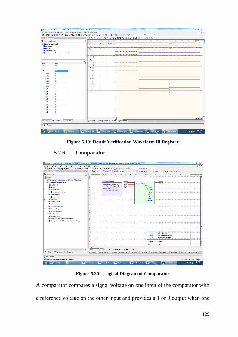
129
Figure 5.19: Result Verification Waveform Bi Register
5.2.6 Comparator
Figure 5.20: Logical Diagram of Comparator
A comparator compares a signal voltage on one input of the comparator with
a reference voltage on the other input and provides a 1 or 0 output when one

130
of the signals is greater than the other. The code and logical block diagram
of comparator is shown in fig 5.20. This comparator has two 16 bit input
signal ‘a’ and ‘b’, and a select signal‘s’. At the output it has a 16 bit output
data line namely as ‘y’.
a_1
=
un1_a
<
y11
<
un1_s
un1_s_1
un1_s_2
un1_s_3
un1_s_4
un1_s_5
un1_s_6
un1_s_7
un1_s_8
un1_s_9
un1_s_10
un1_s_11
y
e
d
e
d
e
d
e
d
e
d
e
d
e
d
e
d
e
d
e
d
e
d
e
d
[15:0]
[15:0]
[15:0]
[15:0]
[15:0]
[15:0]
[5]
[4]
[2]
[3]
[1]
[0]
[5]
[4]
[3]
[2]
[1]
[0]
1
0
1
0
1
0
1
0
1
0
1
0
y
s[0:5][0:5]
b[15:0][15:0]
a[15:0][15:0]
Figure 5.21: RTL View of Comparator

131
The figure 5.21 shows the RTL schematic of the Tri State Register (top)
generated from Synplify pro synthesis tool and simulated outputs are shown
in fig 5.22.
Figure 5.22: Result Verification Waveform Comparator
To verify the result of comparator, for the first 100ns of time period the input
values given for a0 is 1, for b0 is 1, for c1 is 0 and for c2 is also 0.According
to the truth table of bit0 the output values for cout and x0 should be 1 and 0
respectively. It can be clearly shown in the above figure that cout and x0 have
the same value as in the truth table.

132
5.2.7 Control Unit
library event_processor_f... use event_processor...library ieee; use ieee.std_logic_1...
Design Unit Headerprocess (pstate) begin vma <= '0'; wrb <= '0'; outregrd <= outregwr ... pcwr <= '0'; pcrd <= '0'; addregsel ... opregsel <... instregsel ... compsel <= alusel <= ... shiftsel <= regsel <= ... case pstate when res... alusel ...
process (clk,reset) begin if (reset = '1' pstate <= elsif (clk = pstate <= end if; end process;
addregsel
aluselclk
compsel
instregout
instregsel
opregsel
outregrd
outregwr
pcrd
pcwr
ready
regrd
regsel
regwr
reset
shiftsel
vma
wrb
compout
Figure 5.23: Logical Diagram of Control Unit
Control unit is one of the major components of the processing unit. It
provides the timing and control signal to all operations of microcomputer. It
controls the flow of data between microprocessor and memory and
peripherals. Control unit also synchronizes all the operations performed by
the processor. The code and logical block diagram of control unit is shown in

133
fig 5.23. As shown in fig 5.23 various control and timing signals are
generated at the output of the control unit. Simulated output of control unit is
shown in figure 5.24. The control unit has several input signals like clk,
reset, ready etc. and several output signals like alusel, compsel, addregsel
etc. The values are assigned to the input signals and corresponding output
waveform is observed for functional verification of control unit.
Figure 5.24: Result Verification Waveform Control Unit

134
5.2.8 RAM
library ieee; use ieee.std_logic_1164.all; use ieee.std_logic_unsigned.all; use ieee.std_logic_unsigned.all;
Design Unit Header
type ram_mem_type is array (127 downto 0) of std_logic_vector(7 downto 0);
Architecture Declaration
Q <= ram_mem(CONV_I...
block_60
process (CLK) variable A... begin if rising_e... if (WE = ADDR... ram_... end if; end if; end process;
ADDRrd(6:0)
ADDRwr(6:0)
CLK
DATA(7:0)
Q(7:0)
WE
Figure 5.25: Logical Diagram of RAM
The temporary data used during system operation are stored in RAM
(random access memory). The size of RAM and ROM are selected based on
the performance needed and the type of the algorithms used. The code and
logical block diagram of RAM is shown in fig 5.25.

135
ram1
ram_mem[7:0]
[6:0]RADDR[6:0]
[7:0]DATA[7:0]
[7:0]DOUT[7:0][6:0]
WADDR[6:0]
WE
CLK
Q[7:0][7:0]
DATA[7:0][7:0]
ADDRwr[6:0][6:0]
ADDRrd[6:0][6:0]
CLK
WE
Figure 5.26: RTL View of RAM
Figure 5.27: Snap Shot of RTL View of RAM
The figure 5.26-5.27 shows the RTL schematic of the RAM (top) generated
from Synplify pro synthesis tool and simulated outputs are shown in
figure5.28.

136
Figure 5.28: Result Verification Waveform RAM
5.2.9 ROM
library ieee; use ieee.std_logic_1164.all; use ieee.std_logic_unsigned.all; use ieee.std_logic_unsigned.all;
Design Unit Headerprocess (ADDRESS,OE) begin if (OE = '1') case (A... when "... Q <= ... when "... Q <= ... when "... Q <= ...
ADDRESS(10:0)
OE
Q(7:0)
Figure 5.29: Logical Diagram of ROM

137
The coded program instructions are stored in ROM (read-only memory).
There are some special purpose registers such a program counter (PC) to
hold the address of the instruction being fetched from ROM. The code and
logical block diagram of RAM is shown in fig 5.29.The simulated outputs is
shown in fig 5.30.
Figure 5.30: Result Verification Waveform ROM
5.2.10 Latch
library ieee; use ieee.std_logic_1164.all;
Design Unit Headerprocess (GATE,DATA,CLR, begin if CLR = '1' TEMP_Q elsif SET = TEMP_Q elsif GE = ... if GATE = TEMP... end if;
nQ <= not TEMP_Q;
block_63
CLR
DATA(15:0)
GATE
GE
nQ(15:0)
SET
Q(15:0)

138
Figure 5.31: Logical Diagram of Latch
Each port in the system architecture has a latch associated with it. When the
port is used as a destination by the processor always write to latch, while
when the port is the source the processor always reads the port pin. The code
and logical block diagram for latch is shown in figure 5.31.
nQ[15:0] un1_gate
latrs
Q[15:0]
[15:0][15:0]
[15:0]D[15:0]
C [15:0]Q[15:0]
R
S
Q[15:0][15:0]
nQ[15:0][15:0]
DATA[15:0][15:0]
GATE
GE
SET
CLR
Figure 5.32: RTL View of Latch

139
Figure 5.33: Snap Shot of RTL View of Latch
The figure 5.32-5.33 shows the RTL schematic of the Latch (top) generated
from Synplify pro synthesis tool and the simulated output is shown in fig
5.34.
Figure 5.34: Result Verification Waveform of Latch
5.2.11 Event Processor
This VHDL design was modified and improved several times with the
process of test, debug and modify, till the final optimum design was formed.

140
library event_processor_f... use event_processor...library ieee; use ieee.std_logic_1... use ieee.std_logic_u...
Design Unit Headerprocess (a,b,s) begin case s is when add y <= a + when sub y <= a - b when inc... y <= a + when dec
a
b
s
y
library event_processor_f... use event_processor...library ieee; use ieee.std_logic_1... use ieee.std_logic_u...
Design Unit Headerprocess (a,b,s) begin case s is when add y <= a + when sub y <= a - b when inc... y <= a + when dec
a
b
s
y
Figure 5.35: Snapshot of event processor
library event_processor_f... use event_processor...library ieee; use ieee.std_logic_1... use ieee.std_logic_u...
Design Unit Headerprocess (a,b,s) begin case s is when add y <= a + when sub y <= a - b when inc... y <= a + when dec
a
b
s
y
library event_processor_f... use event_processor...library ieee; use ieee.std_logic_1... use ieee.std_logic_u...
Design Unit Headerprocess (a,b,s) begin case s is when add y <= a + when sub y <= a - b when inc... y <= a + when dec
a
b
s
y
library event_processor_f... use event_processor...library ieee; use ieee.std_logic_1... use ieee.std_logic_u...
Design Unit Headerprocess (a,b,s) begin case s is when add y <= a + when sub y <= a - b when inc... y <= a + when dec
a
b
s
y

141
library event_processor_f... use event_processor...library ieee; use ieee.std_logic_1...
Design Unit Headerc lk ad d reg se l
co m po ut aluse l
ins treg o ut co m p se l
re ad y ins treg se l
re se t o p re gse l
o utreg rd
o utreg w r
p crd
p cw r
re g rd
re g se l
re g w r
shif tse l
vm a
w rb
a y
s
a y
b
s
a y
s
a y
b
s
a y
rd
w r
a y
rd
w r
a y
s
a y
s
rd y
s
w r
x
u10
control
u6
bireg
address
u1
alu
u2
shift
clk
u3
compdata
u4
triregu5
trireg
u7
bireg
u8
bireg
u9
regarray
ready
reset
vma
wrb
Figure 5.36: Logical Diagram of event processor
Figure 5.37: Result Verification Waveform of event processor

142
The custom designed processor for WSN node is designed specifically for
the WSN node agricultural application. It is essentially an event driven
processor which responds only to the particular event of interests. Here the
event of interest means significant change in the value of the measured
quantity.
For this it consists of an event detection unit which is essentially an interrupt
controller. It has a comparator which compares the measured data with
threshold. If the output of comparator detects measured value is greater from
threshold then it generates an interrupt signal for processor that an event has
occurred. The rest of the system contains blocks like ALU, Register Array,
control unit, RAM, ROM etc. necessary for processing the data acquired.
5.3 Comparison and analysis of proposed node with
existing nodes
Table 5.1: Comparison of Proposed Node with other nodes Node
CPU Power Memory Radio Latency Sampling
Mode
Mica-Z ATMEGA
128
285mW
active
4K RAM
128K
Flash
250Kbps Low
Continuous
Sampling Telos Motorola
HCS08
120mW
active
4K RAM 250Kbps Low
Rene ATMEL
8535
.036mW
sleep
60mW
active
512B-
RAM 8K
Flash
10Kbps Medium
Time
Triggered Mica-2 ATMEGA
128
.036mW
sleep
60mW
active
4K RAM
128K
Flash
76Kbps Medium
Proposed Custom .021mW 4K RAM 5Kbps High Event

143
WSN
Node
Designed
Event
Processor
Sleep
55mW
active
2K Flash Based
Table 5.1 shows that for the event processor based WSN node power
consumption is reduced significantly. This is because the conventional
processor based WSN node acts even for small changes in values of sensed
quantity, while the event processor based WSN node only works when the
value of sensed parameter changes significantly. Furthermore the event
processor will result in overall improvement in the lifetime of WSN node.
Figure 5.38 Comparison of proposed WSN node with other nodes (Active Power)

144
Figure 5.39 Comparison of proposed WSN node with other nodes (Sleep Power)
Table 5.2: Comparison of Proposed Node Event processor with other nodes
MICA-Z
T-mote XYZ Node Proposed
node
CPU
Type
Atmel (AVR) MSP430(MSP) ML- 67Q500
(ARM 7)
ASIC
CPU
clock
16MHz 8MHz 60 MHz 100KHz
Table 5.2 compares the clock frequency of different processors used for
WSN node with proposed custom designed event processor. From table 5.2
it is clear that the proposed processor works on 100 KHz which is quite low
in comparison to other processors. This low clock frequency results in a
delay in operation execution but reduces the overall power consumption.
This latency in processing is tolerable due to the delay tolerant nature of
agricultural application.

145
Table 5.3: Power Analysis Results for the Proposed Node Event processor
Total power dissipated is 30.1mW.
Table 5.3 shows the power consumption of Proposed Node Event processor,
extracted from XPower Analyser of Xilinx ISE.
As listed in table 5.3, the power consumption of proposed node event
processor is this is due to the reduced clock frequency and customized
architecture for agricultural application.
From table 5.3 it can be observed that the active power consumption for
custom designed processor for WSN node is 30.1mW.
Name Value Used Total Available Utilization (%)
Clocks 0.00108 (W) 1 ----
Logic 0.00071 (W) 3844 17344 22.2
Signals 0.00152 (W) 5071 ----
IOs 0.00026 (W) 32 250 12.8
BRAMs 0.00001 (W) 2 28 7.1
DCMs 0.0019 (W) 1 8 12.5
MULTs 0.00001 (W) 6 28 21.4 Total Quiescent
Power 0.02462 (W) Total Dynamic
Power 0.00548 (W)
Total Power 0.0301 (W)
Junction Temp 30.6 (degrees
C)

146
Figure 5.40: Power consumption of event processor
Figure 5.41: Power consumption of different components of event processor
The figure 5.41 shows the power consumption by the different blocks of
custom designed processor. This power consumption was estimated using
the XPower Analyser of Xilinx ISE.

147
Figure 5.42: Percentage utilization of different components of event processor
5.4 Summary of the Chapter
The goal of the chapter was to implement a customizable processing unit for
WSN node. To achieve this goal it is required to have not only a working
RTL model but also synthesize, place & route the design. This design, posed
various design problems. Therefore, testing the functionality of the design
after each design step – synthesis, clock tree insertion, and routing was
important. For this purpose simulation of the design net-list was done using
Active HDL 6.3 sp3.
Simulation results after the stages – RTL design, synthesis, clock tree
insertions are shown in the chapter. Final post-layout back-annotation
simulation was done to test if the design was properly placed and routed. For
this purpose a standard delay file (SDF) of the design was generated using
the Hyper-extract tool. Figure 5.36 and 5.37 shows the simulation using

148
Active HDL 6.3 sp3 with delay information provided by the SDF file. The
baseline Customizable logic controller was operated up to a speed of 25
MHz with basic timing constraints. There is a significant improvement in
terms of power consumption by using the custom designed event processor
for WSN node. Finally all the units were exported and modeled in NI Circuit
Design Suite for co-simulation of various models developed. Also prototype
hardware was developed to practically test the WSN node.
After analyzing the results, a numerical comparative study was done based
on the proposed WSN node and existing nodes as shown in figure 5.38 and
5.39. Furthermore the event processor resulted in overall improvement in
terms of power consumption in comparison to a general purpose processor.
Power consumption of event processor, power consumption of its
components and percentage of area utilization are shown in figure 5.40, 5.41
and 5.42 respectively.
149
CHAPTER 6:
Conclusions and
Future Research
A summary of the work contained in the
various chapters of this thesis is presented
along with some suggestions for future
research work.

150
CHAPTER 6: Conclusions & Future Research
6.1 Conclusions
In the present work, the design and implementation of WSN Node was
discussed and also a test environment was built to verify its functionality.
With the help of simulation tools, the input information was entered and
observed whether the WSN node is functioning properly or not.
The designed WSN node had the advantage that at each phase of the design
the functional simulation has very consistent checking procedures. The
verification methodology involving functional simulation helps to detect
error early in the design flow. From the IC specification to the final
implementation phases are defined and implemented. Before physically
manufacturing an electronic circuit, an important stage is the simulation of
its behavior in order to check its optimal functioning. SPICE is one of the
most used simulators for analog circuits. In order to build models on basis of
the equations VHDL-AMS was used [199 - 200], one of the languages that
support the analog circuits description on basis of ordinary differential
algebraic equations (ODAE) in order to complete the support needed to

151
describe and simulate discrete events. VHDL-AMS and its capability to
provide communication between discrete events and continuous time
systems, allows the creation of very complex models for the functioning of
analog, digital and mixed signals electronic circuits. MULTISIM,
manufactured by National Instruments, is a program conceived for the
simulation of circuits that allow users to simulate circuit. Active HDL,
Syplify Pro and Xilinx ISE were used for writing and checking the VHDL
code for the custom designed processor for WSN node. Many adjustments
through scripts and coding were done to achieve the final design and its
implementation.
Finally using a standard and matured design flow , with clearly design steps ,
powerful and proven software tools (Active HDL 8.1 and Synplify Pro 7.1),
specified check points and rigorous verification procedures standard outputs
( result verification waveforms , RTL view and Synthesis Report) and
documentation was generated.
• Hardware implementation of WSN node was done and power
consumption was calculated.
• Simulation of Custom Designed Processor for WSN node was
done and power consumption was calculated.
• Comparison of proposed node was done with two other nodes and
results were comprehensively documented.

152
6.2 Directions for future research
The future research work would focus on improving the design of WSN
node by integrating the sensors and transceiver on single substrate.
Improving the issue of mixed signal components and providing power to
them is also to be explored [201]. The research would also focus on finding
the new verticals where the significance of WSN node would increase the
profit of farmer at least twice. The research would be on the principles of
WSN node for agricultural application to find various parameters that can be
sensed to obtain maximum yield [202]. To achieve this whole new
generation of sensors will be required to sense the desired parameters. This
opens a new avenue for further research of multi-sensor data fusion. These
developments in future will come Along with a requirement of data
aggregation technique to reduce the data collected by the node.
It should also be understood that some advanced analytical techniques could
be too complex to understand and implement [203]. The real implementation
of WSN node with all the sensors and analog components like transceiver,
ADC etc. integrated on one substrate would be very difficult. This is the
limitation and future scope of our research. We believe that future work on
stated framework would be to study and analyze the various factors that will
come in to picture while integrating all the components on the single
substrate.

153
Furthermore some sort of energy scavenging scheme may be used not only
to increase the lifetime of the node but also the productivity of the network
[204].
The determination of suitable energy scavenging scheme for a particular
application can be taken for investigation in future there is a wide scope of
doing work in this area. This is discussed briefly in chapter-2 and it can be
extended for selecting appropriate energy scavenging scheme.
Wireless Sensor Network technology offers significant potential in numerous
applications. However, there are significant amount of technical challenges
and design issues those needs to be addressed.

154
APPENDIX A:
Bibliography &
List of websites visited
155
Bibliography [1]. Robert M. Crovella (1999), ‘Sensor Networks and Communication’, CRC Press
LLC.
[2]. Raghunathan, V., Schurgers, C., Sung Park, Srivastava, M.B., (2002), ‘Energy-
aware wireless microsensor networks,’ IEEE Signal Processing Magazine, vol.19,
no.2, pp.40-50. doi: 10.1109/79.985679
[3]. Ruihua Zhang, Dongfeng Yuan, Quanquan Liang (2007), ‘Analysis of Energy
Consumption and Lifetime of Wireless Sensor Networks,’ 2nd IEEE Conference
on Industrial Electronics and Applications, ICIEA 2007, pp.1159-1164. doi:
10.1109/ICIEA.2007.4318589
[4]. SuraiyaTarannum (2011), ‘Wireless Sensor Networks, 2nd ed.’, InTech Croatia.
[5]. Mark Hempstead, Nikhil Tripathi, Patrick Mauro, Gu-Yeon Wei, David Brooks,
(2005), ‘An Ultra Low Power System Architecture for Sensor Network
Applications’, Proceedings of the 32nd International Symposium on Computer
Architecture (ISCA’05), IEEE, pp. 208-219. doi: 10.1109/ISCA.2005.12
[6]. Wightman, P.M., Labrador, M.A., 2010, ‘LatinCon16 - Topology Maintenance:
Extending the Lifetime of Wireless Sensor Networks,’ IEEE (Revista IEEE
America Latina) Latin America Transactions, vol.8, no.4, pp.469-475. doi:
10.1109/TLA.2010.5595139
[7]. Shah-Mansouri, V., Wong, V., (2010), ‘Lifetime-resource tradeoff for multicast
traffic in wireless sensor networks,’ IEEE Transactions onWireless
Communications, vol.9, no.6, pp.1924-1934. doi: 10.1109/TWC.2010.06.081631
[8]. Kasbekar, G.S., Bejerano, Y., Sarkar, S., (2011), ‘Lifetime and Coverage
Guarantees Through Distributed Coordinate-Free Sensor Activation,’ IEEE/ACM
Transactions on Networking, vol.19, no.2, pp.470-483. doi:
10.1109/TNET.2010.2077648
[9]. Virantha N. Ekanayake, Clinton Kelly IV, and Rajit Manohar (2004), ‘An ultra
low-power processor for sensor networks’, In Proceedings of the ACM
Conference on Architectural Support for Programming Languages and Operating
Systems (ASPLOS XI), pages 27–36.
[10]. Abbasi, A. A., Younis, M. F., Baroudi, U. A., (2013), ‘Recovering From a Node
Failure in Wireless Sensor-Actor Networks With Minimal Topology

156
Changes,’ IEEE Transactions on Vehicular Technology, vol.62, no.1, pp.256-271.
doi: 10.1109/TVT.2012.2212734
[11]. Ahmed, M.F.A., Vorobyov, S.A., (2009), ‘Collaborative beamforming for
wireless sensor networks with Gaussian distributed sensor nodes,’ IEEE
Transactions on Wireless Communications, vol.8, no.2, pp.638-643. doi:
10.1109/TWC.2009.071339
[12]. Baoqiang, Kan, Li, Cai, Hongsong, Zhu, Yongjun, Xu, (2008), ‘Accurate energy
model for WSN node and its optimal design,’ Journal of Systems Engineering and
Electronics, vol.19, no.3, pp.427-433. doi: 10.1016/S1004-4132(08)60102-4
[13]. Chong, C.-Y., Kumar, S. P. (2003), ‘Sensor networks: Evolution, opportunities,
and challenges’, Proc. IEEE Volume 91, No. 8, pp. 1247-1256.
[14]. Dargie, W.,( 2012), ‘Dynamic Power Management in Wireless Sensor Networks:
State-of-the-Art,’ IEEE Sensors Journal, vol.12, no.5, pp.1518-1528. doi:
10.1109/JSEN.2011.2174149
[15]. Demin Wang, Bin Xie, Agrawal, D.P., (2008), ‘Coverage and Lifetime
Optimization of Wireless Sensor Networks with Gaussian Distribution,’ IEEE
Transactions onMobile Computing, vol.7, no.12, pp.1444-1458. doi:
10.1109/TMC.2008.60
[16]. Deng, S., Li, J., Shen, L., (2011), ‘Mobility-based clustering protocol for wireless
sensor networks with mobile nodes,’ Wireless Sensor Systems, IET , vol.1, no.1,
pp.39-47. doi: 10.1049/iet-wss.2010.0084
[17]. E. Niewiadomska-Szynkiewicz, P. Kwaśniewski, and I. Windyga (2009),
‘Comparative study of wireless sensor networks energy-efficient topologies and
power save protocols’, Journal of Telecommunication and Information
Technology, Volume. 3, pp. 68–75.
[18]. Gang Wang, Kehu Yang, (2011) , ‘A New Approach to Sensor Node Localization
Using RSS Measurements in Wireless Sensor Networks,’ IEEE Transactions
on Wireless Communications, vol.10, no.5, pp.1389-1395. doi:
10.1109/TWC.2011.031611.101585
[19]. GianPietroPicco Wendi Heinzelman (2012), ‘Wireless Sensor Networks’,
Proceedings of 9th European Conference, EWSN 2012, Trento, Italy.
[20]. GürhanKüçük, Can Basaran (2006), ‘Power-Aware processors for wireless sensor
networks’, Proceedings of the 21st international conference on Computer and
Information Sciences, pp. 655-664. Doi: 10.1007/11902140_69
157
[21]. HainingShu, Qilian Liang, Jean Gao, (2008), ‘Wireless Sensor Network Lifetime
Analysis Using Interval Type-2 Fuzzy Logic Systems,’ IEEE Transactions on
Fuzzy Systems, vol.16, no.2, pp.416-427. doi: 10.1109/TFUZZ.2006.890668
[22]. Henri Dubois-Ferriere, Roger Meier, Laurent Fabre, Pierre Metrailler (2006),
‘TinyNode: A Comprehensive Platform for Wireless Sensor Network
Applications’, ACM-IPSN’06, Nashville, Tennessee, USA.
[23]. Hongyang Chen, Gang Wang, Zizhuo Wang, So, H.C., Poor, H.V., (2012), ‘Non-
Line-of-Sight Node Localization Based on Semi-Definite Programming in
Wireless Sensor Networks,’ IEEE Transactions on Wireless
Communications, vol.11, no.1, pp.108-116. doi:
10.1109/TWC.2011.110811.101739
[24]. Hou, Y.T., Yi Shi, Sherali, H.D., (2008), ‘Rate Allocation and Network Lifetime
Problems for Wireless Sensor Networks,’ IEEE/ACM Transactions on
Networking, vol.16, no.2, pp.321-334. doi: 10.1109/TNET.2007.900407
[25]. Hou, Y.T., Yi Shi, Sherali, H.D., Midkiff, S.F., (2005), ‘On energy provisioning
and relay node placement for wireless sensor networks,’ IEEE Transactions
on Wireless Communications, vol.4, no.5, pp. 2579- 2590.
doi: 10.1109/TWC.2005.853969
[26]. Huei-Wen Ferng, Hadiputro, M., Kurniawan, A., (2011), ‘Design of Novel Node
Distribution Strategies in Corona-Based Wireless Sensor Networks,’ IEEE
Transactions on Mobile Computing, vol.10, no.9, pp.1297-1311. doi:
10.1109/TMC.2010.241
[27]. Hui Wang, Yuhang Yang, Maode Ma, Jianhua He, Xiaomin Wang, (2008),
‘Network lifetime maximization with cross-layer design in wireless sensor
networks,’ IEEE Transactions on Wireless Communications, vol.7, no.10,
pp.3759-3768, October
doi: 10.1109/T-WC.2008.070079
[28]. Ioan Raicu (2003), ‘Efficient Even Distribution of Power Consumption in
Wireless Sensor Network’, ISCA 18th Int'l Conf. on Computers and Their
Applications, CATA'03, Honolulu, Hawaii, USA, 2003.
[29]. J. Glaser, D. Weber, S. Madani, S. Mahlknecht (2008), ‘Power aware simulation
framework for wireless sensor networks and nodes’, EURASIP J. Embedded
Syst., vol. 2008, pp.1 -16. doi:10.1155/2008/369178
158
[30]. Jokhio, S.H., Jokhio, I.A., Kemp, A.H., (2012), ‘Node capture attack detection
and defence in wireless sensor networks,’ Wireless Sensor Systems, IET, vol.2,
no.3, pp.161-169. doi: 10.1049/iet-wss.2011.0064
[31]. Jun Luo, Hubaux, J.-P., (2010), ‘Joint Sink Mobility and Routing to Maximize the
Lifetime of Wireless Sensor Networks: The Case of Constrained Mobility,’
IEEE/ACM Transactions on Networking, vol.18, no.3, pp.871-884. doi:
10.1109/TNET.2009.2033472
[32]. Junlin Li, AlRegib, G., (2009), ‘Network Lifetime Maximization for Estimation in
Multihop Wireless Sensor Networks,’ IEEE Transactions on Signal Processing,
vol.57, no.7, pp.2456-2466. doi: 10.1109/TSP.2009.2016872
[33]. JunniZou, Hongkai Xiong, Chenglin Li, Ruifeng Zhang, Zhihai He, (2011),
‘Lifetime and Distortion Optimization With Joint Source/Channel Rate
Adaptation and Network Coding-Based Error Control in Wireless Video Sensor
Networks,’ IEEE Transactions on Vehicular Technology, vol.60, no.3, pp.1182-
1194. doi: 10.1109/TVT.2011.2111425
[34]. Jun-Won Ho, Wright, M., Das, S.K., (2011), ‘Fast Detection of Mobile Replica
Node Attacks in Wireless Sensor Networks Using Sequential Hypothesis
Testing,’ IEEE Transactions on Mobile Computing, vol.10, no.6, pp.767-782. doi:
10.1109/TMC.2010.213
[35]. Jun-Won Ho, Wright, M., Das, S.K., (2012), ‘ZoneTrust: Fast Zone-Based Node
Compromise Detection and Revocation in Wireless Sensor Networks Using
Sequential Hypothesis Testing,’ IEEE Transactions on Dependable and Secure
Computing, vol.9, no.4, pp.494-511. doi: 10.1109/TDSC.2011.65
[36]. Karkvandi, H.R., Pecht, E., Yadid-Pecht, O., (2011), ‘Effective Lifetime-Aware
Routing in Wireless Sensor Networks,’ IEEE Sensors Journal, vol.11, no.12,
pp.3359-3367. doi: 10.1109/JSEN.2011.2159110
[37]. Kaur, T., Jinsuk Baek, (2009), ‘A strategic deployment and cluster-header
selection for wireless sensor networks,’ IEEE Transactions on Consumer
Electronics, vol.55, no.4, pp.1890-1897. doi: 10.1109/TCE.2009.5373747
[38]. Kenan Xu, Hassanein, H., Takahara, G., Quanhong Wang, (2010), ‘Relay Node
Deployment Strategies in Heterogeneous Wireless Sensor Networks,’ IEEE
Transactions on Mobile Computing, vol.9, no.2, pp.145-159. doi:
10.1109/TMC.2009.105

159
[39]. Klaoudatou, E., Konstantinou, E., Kambourakis, G., Gritzalis, S., (2011), ‘A
Survey on Cluster-Based Group Key Agreement Protocols for WSNs,’ IEEE
Communications Surveys & Tutorials, vol.13, no.3, pp.429-442. doi:
10.1109/SURV.2011.061710.00109
[40]. Koubaa, A., Severino, R., Alves, M., Tovar, E., (2009), ‘Improving Quality-of-
Service in Wireless Sensor Networks by Mitigating ‘Hidden-Node
Collisions’,’ IEEE Transactions on Industrial Informatics, , vol.5, no.3, pp.299-
313. doi: 10.1109/TII.2009.2026643
[41]. Lloyd, E.L., Guoliang Xue (2007), ‘Relay Node Placement in Wireless Sensor
Networks,’ IEEE Transactions on Computers, vol.56, no.1, pp.134-138. doi:
10.1109/TC.2007.250629
[42]. Luis Ruiz-Garcia, Loredana Lunadei, Pilar Barreiro, Jose Ignacio Robla (2009),
‘A Review of Wireless Sensor Technologies and Applications in Agriculture and
Food Industry: State of the Art and Current Trends’, Sensors 2009, Volume 9, pp.
4728-4750. doi:10.3390/s90604728
[43]. Luo R.C., Chen O. (2012), ‘Mobile Sensor Node Deployment and Asynchronous
Power Management for Wireless Sensor Networks,’ IEEE Transactions on
Industrial Electronics, vol.59, no.5, pp.2377-2385. doi:
10.1109/TIE.2011.2167889
[44]. Macedo, M., (2009), ‘Are there so many sons per node in a wireless sensor
network data aggregation tree?,’ IEEE Communications Letters, vol.13, no.4,
pp.245-247. doi: 10.1109/LCOMM.2009.082003
[45]. Madan, R., Lall, S., (2006), ‘Distributed algorithms for maximum lifetime routing
in wireless sensor networks,’ IEEE Transactions on Wireless Communications,
vol.5, no.8, pp.2185-2193. doi: 10.1109/TWC.2006.1687734
[46]. Maheswararajah, S., Halgamuge, S.K., Dassanayake, K.B., Chapman, D., ( 2011),
‘Management of Orphaned-Nodes in Wireless Sensor Networks for Smart
Irrigation Systems,’ IEEE Transactions on Signal Processing, vol.59, no.10,
pp.4909-4922. doi: 10.1109/TSP.2011.2160258
[47]. Matamoros, J., Anton-Haro, C., (2010), ‘Opportunistic power allocation and
sensor selection schemes for wireless sensor networks,’ IEEE Transactions on
Wireless Communications, vol.9, no.2, pp.534-539. doi:
10.1109/TWC.2010.02.090215
160
[48]. Misra, S., Seung Don Hong, GuoliangXue, Jian Tang, (2010), ‘Constrained Relay
Node Placement in Wireless Sensor Networks: Formulation and Approximations,’
IEEE/ACM Transactions on Networking, vol.18, no.2, pp.434-447.doi:
10.1109/TNET.2009.2033273
[49]. Natalizio, E., Loscri, V., Guerriero, F., Violi, A., (2009), ‘Energy spaced
placement for bidirectional data flows in wireless sensor network,’ IEEE
Communications Letters, vol.13, no.1, pp.22-24. doi:
10.1109/LCOMM.2009.081774
[50]. Okorafor, U.N., Kundur, D., (2009), ‘On the Relevance of Node Isolation to the
K-Connectivity of Wireless Optical Sensor Networks,’ IEEE Transactions on
Mobile Computing, vol.8, no.10, pp.1427-1440. doi: 10.1109/TMC.2009.57
[51]. Phan, K.T., Rongfei Fan, Hai Jiang, Vorobyov, S.A., Tellambura, C., (2009),
‘Network Lifetime Maximization With Node Admission in Wireless Multimedia
Sensor Networks,’ IEEE Transactions on Vehicular Technology, vol.58, no.7,
pp.3640-3646. doi: 10.1109/TVT.2009.2013235
[52]. Prasad V., Son S.H. (2007), ‘Classification of Analysis Techniques for Wireless
Sensor Networks,’ Fourth International Conference on Networked Sensing
Systems, INSS '07, pp.93-97. doi: 10.1109/INSS.2007.4297397
[53]. Quanhong Wang, Kenan Xu, Takahara, G., Hassanein, H., (2007), ‘Transactions
Papers - Device Placement for Heterogeneous Wireless Sensor Networks:
Minimum Cost with Lifetime Constraints,’ IEEE Transactions on Wireless
Communications, vol.6, no.7, pp.2444-2453. doi: 10.1109/TWC.2007.05357
[54]. Quanjun Chen, Kanhere, S.S., Hassan, M., (2009), ‘Analysis of per-node traffic
load in multi-hop wireless sensor networks,’ IEEE Transactions on Wireless
Communications, vol.8, no.2, pp.958-967. doi: 10.1109/TWC.2009.080008
[55]. Qun Zhao, Gurusamy, M., (2008), ‘Lifetime Maximization for Connected Target
Coverage in Wireless Sensor Networks,’ IEEE/ACM Transactions on
Networking, vol.16, no.6, pp.1378-1391. doi: 10.1109/TNET.2007.911432
[56]. Radeke, R., Marandin, D., Claudios, F.J., Todorova, P., Tomic, S., (2008), ‘On
reconfiguration in case of node mobility in clustered wireless sensor
networks,’ IEEE Wireless Communications, vol.15, no.6, pp.47-53, December
doi: 10.1109/MWC.2008.4749747

161
[57]. Rahman, MdNafees, Matin, M A, (2011), ‘Efficient algorithm for prolonging
network lifetime of wireless sensor networks,’ Tsinghua Science and Technology,
vol.16, no.6, pp.561-568. doi: 10.1016/S1007-0214(11)70075-X
[58]. S. Anandamurugan, C. Venkatesh (2010), ‘Reducing Power Consumption in
Wireless Sensor Networks by using Terrain Based Probabilistic Forwarding
Scheme (TBPFS),’ IJCSNS International Journal of Computer Science and
Network Security, Vol.10 No.2, February 2010, pp. 208-217.
[59]. See, C.H., Horoshenkov, K.V., Abd-Alhameed, R.A., Yim Fun Hu, Tait, S.J.,
(2012), ‘A Low Power Wireless Sensor Network for Gully Pot Monitoring in
Urban Catchments,’ IEEE Sensors Journal, vol.12, no.5, pp.1545-1553. doi:
10.1109/JSEN.2011.2174354
[60]. Seema, A., Reisslein, M., (2011), ‘Towards Efficient Wireless Video Sensor
Networks: A Survey of Existing Node Architectures and Proposal for A Flexi-
WVSNP Design,’ IEEE Communications Surveys & Tutorials, vol.13, no.3,
pp.462-486. doi: 10.1109/SURV.2011.102910.00098
[61]. Taeksang Song, Hyoung-Seok Oh, Yoon, E., Hong, S., (2007), ‘A Low-Power
2.4-GHz Current-Reused Receiver Front-End and Frequency Source for Wireless
Sensor Network,’ IEEE Journal of Solid-State Circuits, vol.42, no.5, pp.1012-
1022. doi: 10.1109/JSSC.2007.894338
[62]. Tavli, B., Akgun, M.B., Bicakci, K., (2011), ‘Impact of Limiting Number of Links
on the Lifetime of Wireless Sensor Networks,’ IEEE Communications Letters,
vol.15, no.1, pp.43-45. doi: 10.1109/LCOMM.2010.111910.101846
[63]. Tavli, B., Bagci, I.E., Ceylan, O., (2010), ‘Optimal data compression and
forwarding in wireless sensor networks,’ IEEE Communications Letters, vol.14,
no.5, pp.408-410. doi: 10.1109/LCOMM.2010.05.092372
[64]. Thilagam, B.R., Prakash, K.S.S., (2007), ‘An Adaptive Communication Model for
Large Wireless Sensor Networks,’ 2nd International Conference on Pervasive
Computing and Applications, ICPCA 2007, pp.484-489. doi:
10.1109/ICPCA.2007.4365492
[65]. A. Baggio, “Wireless sensor networks in precision agriculture”, in ACM
Workshop on Real-World Wireless Sensor Networks (REALWSN 2005),
Stockholm, Sweden, June 2005.

162
[66]. Wu, Xiao Ping, Tan, ShiLi, Chen, Tao, Yi, Xiaomei, Dai, Dan, (2011),
‘Distributed dynamic navigation for sensor networks,’ Tsinghua Science and
Technology, vol.16, no.6, pp.648-656. doi: 10.1016/S1007-0214(11)70085-2
[67]. Xiaobing Wu, Guihai Chen, Das, S.K., (2008), ‘Avoiding Energy Holes in
Wireless Sensor Networks with Nonuniform Node Distribution,’ IEEE
Transactions on Parallel and Distributed Systems, vol.19, no.5, pp.710-720. doi:
10.1109/TPDS.2007.70770
[68]. Xueyan Tang, Jianliang Xu, (2008), ‘Adaptive Data Collection Strategies for
Lifetime-Constrained Wireless Sensor Networks,’ IEEE Transactions on Parallel
and Distributed Systems, vol.19, no.6, pp.721-734. doi: 10.1109/TPDS.2008.27
[69]. Xueyan Tang, Jianliang Xu, (2008), ‘Optimizing Lifetime for Continuous Data
Aggregation With Precision Guarantees in Wireless Sensor Networks,’
IEEE/ACM Transactions on Networking, vol.16, no.4, pp.904-917. doi:
10.1109/TNET.2007.902699
[70]. Yang, Zheng, Liu, Yunhao, (2012), ‘Understanding Node Localizability of
Wireless Ad Hoc and Sensor Networks,’ IEEE Transactions on Mobile
Computing, vol.11, no.8, pp.1249-1260. doi: 10.1109/TMC.2011.122
[71]. Yaxiong Zhao, Jie Wu, Feng Li, Sanglu Lu, (2012), ‘On Maximizing the Lifetime
of Wireless Sensor Networks Using Virtual Backbone Scheduling,’ IEEE
Transactions on Parallel and Distributed Systems, vol.23, no.8, pp.1528-1535. doi:
10.1109/TPDS.2011.305
[72]. Burrell, J., Brooke, T.; Beckwith, R., (2004), ‘Vineyard computing: sensor
networks in agricultural production,’ IEEE Pervasive Computing, vol.3, no.1, pp.
38- 45. doi: 10.1109/MPRV.2004.1269130
[73]. Mampentzidou, Ioanna, Eirini Karapistoli, Anastasios A. Economides, ‘Basic
Guidelines for Deploying Wireless Sensor Networks in Agriculture’, IEEE
available online: www.flexlearn.uom.gr/conta/publications/PDF/PID2514617.pdf
[74]. B. Pereira, C. C. Shock (2006), ‘Development of irrigation best management
practices for potato from a research perspective in the United States’, Sakia.org e-
publish, Vol. 1,Issue.1, pp.1-20
[75]. Ahonen, T., Virrankoski, R., Elmusrati, M., (2008), ‘Greenhouse Monitoring with
Wireless Sensor Network’, IEEE/ASME International Conference on Mechtronic
and Embedded Systems and Applications, MESA-2008. pp.403 – 408.

163
[76]. G.J. Bishop-Hurley, D.L. Swain, D.M. Anderson, P. Sikka, C. Crossman, P.
Corke (2007), ‘Virtual fencing applications: Implementing and testing an
automated cattle control system’, Elsevier - Computers and Electronics in
Agriculture, Volume 56, pp. 14–22. doi:10.1016/j.compag.2006.12.003
[77]. Yifeng He, Lee, I., Ling Guan, (2009), ‘Distributed Algorithms for Network
Lifetime Maximization in Wireless Visual Sensor Networks,’ IEEE Transactions
on Circuits and Systems for Video Technology, vol.19, no.5, pp.704-718. doi:
10.1109/TCSVT.2009.2017411
[78]. Senel, F., Younis, M.F., Akkaya, K., (2011), ‘Bio-Inspired Relay Node Placement
Heuristics for Repairing Damaged Wireless Sensor Networks,’ IEEE Transactions
on Vehicular Technology, vol.60, no.4, pp.1835-1848. doi:
10.1109/TVT.2011.2131158
[79]. W.S. Lee, V. Alchanatis, C. Yang, M. Hirafuji, D. Moshou, C.Li (2010), ‘Sensing
technologies for precision specialty crop production’, Elsevier - Computers and
Electronics in Agriculture Volume 74, pp.2–33.
[80]. João Valente, David Sanz, Antonio Barrientos, Jaime del Cerro, Ángela Ribeiro,
Claudio Rossi (2011), ‘An Air-Ground Wireless Sensor Network for Crop
Monitoring’, Sensors 2011, Volume 11, pp.6088-6108. doi:10.3390/s110606088
[81]. Ning Wang, Naiqian Zhang, Maohua Wang (2006), ‘Wireless sensors in
agriculture and food industry—Recent development and future perspective’,
Elsevier - Computers and Electronics in Agriculture, Volume 50, pp. 1–14.
doi:10.1016/j.compag.2005.09.003
[82]. Muhamad Azman Miskam, Azwan bin Nasirudin, Inzarulfaisham Abd. Rahim
(2009), ‘Preliminary Design on the Development of Wireless Sensor Network for
Paddy Rice Cropping Monitoring Application in Malaysia’, European Journal of
Scientific Research, Vol.37 No.4, pp.649-657
[83]. Pabari, J.P., Acharya, Y.B., Desai, U.B., Merchant, S.N.,(2012), ‘Development of
Impedance-Based Miniaturized Wireless Water Ice Sensor for Future Planetary
Applications,’ IEEE Transactions on Instrumentation and Measurement, vol.61,
no.2, pp.521-529. doi: 10.1109/TIM.2011.2164292
[84]. Santhosh Simon and K Poulose Jacob (2011), ‘Preliminary Design on the
Development of Wireless Sensor Network for Water Table Monitoring in Paddy
Fields’ , International Journal of Distributed and Parallel Systems (IJDPS) Vol.2,
No.5, pp. 87-93. DOI : 10.5121/ijdps.2011.2508
164
[85]. Markham and A. Wilkinson (2007), ‘Ecolocate: A heterogeneous wireless
network system for wildlife tracking’, In International Joint Conferences on
Computer, Information and Systems Sciences and Engineering (CISSE’07).
[86]. Tim Wark, Peter Corke, Pavan Sikka, Lasse Klingbeil, Ying Guo, Chris
Crossman, Phil Valencia, Dave Swain, Greg Bishop-Hurley (2007),
‘Transforming Agriculture through Pervasive Wireless Sensor Networks’, IEEE
Computer Society, pp.50-57. doi: 10.1109/MPRV.2007.47
[87]. AlShawi, I. S., Yan, L., Pan, W., Luo, B., (2012), ‘Lifetime Enhancement in
Wireless Sensor Networks Using Fuzzy Approach and A-Star Algorithm,’ IEEE
Sensors Journal, vol.12, no.10, pp.3010-3018. doi: 10.1109/JSEN.2012.2207950
[88]. Anastasi, G., Conti, M., Di Francesco, M., (2009), ‘Extending the Lifetime of
Wireless Sensor Networks Through Adaptive Sleep,’ IEEE Transactions on
Industrial Informatics, vol.5, no.3, pp.351-365. doi: 10.1109/TII.2009.2025863
[89]. Arifler, D., (2008), ‘Information Theoretic Approach to Detecting Systematic
Node Destructions in Wireless Sensor Networks,’ IEEE Transactions on Wireless
Communications, vol.7, no.11, pp.4730-4738. doi: 10.1109/T-WC.2008.071001
[90]. Ashouri, M., Zali, Z., Mousavi, S.R., Hashemi, M.R., (2012), ‘New optimal
solution to disjoint set K-coverage for lifetime extension in wireless sensor
networks,’ Wireless Sensor Systems, IET , vol.2, no.1, pp.31-39. doi: 10.1049/iet-
wss.2011.0085
[91]. Bertrand, A., Moonen, M., (2011), ‘Distributed Adaptive Estimation of Node-
Specific Signals in Wireless Sensor Networks With a Tree Topology,’ IEEE
Transactions on Signal Processing, vol.59, no.5, pp.2196-2210.
doi: 10.1109/TSP.2011.2108290
[92]. Beutel, J., Kasten, O., Mattern, F., Römer, K., Siegemund, F., Thiele, L. (2004)
‘Prototyping wireless sensor network applications with bT nodes’, In: Karl, H.,
Wolisz, A., Willig, A. (eds.) EWSN 2004. LNCS, vol. 2920, pp. 323–338.
Springer, Heidelberg.
[93]. Caione, C., Brunelli, D., Benini, L., (2012), ‘Distributed Compressive Sampling
for Lifetime Optimization in Dense Wireless Sensor Networks,’ IEEE
Transactions on Industrial Informatics, vol.8, no.1, pp.30-40. doi:
10.1109/TII.2011.2173500
[94]. Cheong P., Ka-Fai Chang, Ying-Hoi Lai, Sut-Kam Ho, Iam-Keong Sou, Kam-
Weng Tam, (2011), ‘A ZigBee-Based Wireless Sensor Network Node for
165
Ultraviolet Detection of Flame,’ IEEE Transactions on Industrial Electronics, ,
vol.58, no.11, pp.5271-5277. doi: 10.1109/TIE.2011.2119455
[95]. Chiasserini, C.-F., Garetto, M., (2006), ‘An Analytical Model for Wireless Sensor
Networks with Sleeping Nodes,’ IEEE Transactions on Mobile Computing, vol.5,
no.12, pp.1706-1718. doi: 10.1109/TMC.2006.175
[96]. Chung-Ching Shen, Kupershtok R., Bo Yang, Vanin F.M., Xi Shao, Sheth D.,
Goldsman, N., Balzano Q., Bhattacharyya S.S. (2007), ‘Compact, Low Power
Wireless Sensor Network System for Line Crossing Recognition,’ IEEE
International Symposium on Circuits and Systems, ISCAS 2007, pp.2506-2509.
doi: 10.1109/ISCAS.2007.378748
[97]. Cohen, K., Leshem, A., (2010), ‘A Time-Varying Opportunistic Approach to
Lifetime Maximization of Wireless Sensor Networks,’ IEEE Transactions on
Signal Processing, vol.58, no.10, pp.5307-5319. doi: 10.1109/TSP.2010.2052459
[98]. Crosby, G.V., Pissinou, N. (2007), ‘Evolution of Cooperation in Multi-Class
Wireless Sensor Networks,’ 32nd IEEE Conference on Local Computer
Networks, LCN 2007, pp.489-495. doi: 10.1109/LCN.2007.149
[99]. El-Moukaddem, F., Torng, E., Guoliang Xing, Torng, E., Xing, G., Xing, G.,
(2013), ‘Mobile Relay Configuration in Data-Intensive Wireless Sensor
Networks,’ IEEE Transactions on Mobile Computing, vol.12, no.2, pp. 261-273.
doi: 10.1109/TMC.2011.266
[100]. Enayati, A., Brebels, S., De Raedt, W., Vandenbosch, G.A.E. (2011), ‘3D-
Antenna-in-Package Solution for Microwave Wireless Sensor Network Nodes,’
IEEE Transactions on Antennas and Propagation, vol.59, no.10, pp.3617-3623.
doi: 10.1109/TAP.2011.2163779
[101]. Feng Wang, Dan Wang, Jiangchuan Liu, (2011), ‘Traffic-Aware Relay Node
Deployment: Maximizing Lifetime for Data Collection Wireless Sensor
Networks,’ IEEE Transactions on Parallel and Distributed Systems, vol.22, no.8,
pp.1415-1423. doi: 10.1109/TPDS.2011.20
[102]. Hae-Moon Seo, Yeonkug Moon, Yong-Kuk Park, Dongsu Kim, Dong-Sun Kim,
Youn-Sung Lee, Kwang-Ho Won, Seong-Dong Kim, Pyung Choi, (2007), ‘A
Low Power Fully CMOS Integrated RF Transceiver IC for Wireless Sensor
Networks,’ IEEE Transactions on Very Large Scale Integration (VLSI) Systems, ,
vol.15, no.2, pp.227-231. doi: 10.1109/TVLSI.2007.893586

166
[103]. Jae-Hwan Chang, Tassiulas, L., (2004), ‘Maximum lifetime routing in wireless
sensor networks,’ IEEE/ACM Transactions on Networking, vol.12, no.4, pp. 609-
619. doi: 10.1109/TNET.2004.833122
[104]. Joonsung Bae, Kiseok Song, Hyungwoo Lee, Hyunwoo Cho, Hoi-Jun Yoo,
(2012), ‘A Low-Energy Crystal-Less Double-FSK Sensor Node Transceiver for
Wireless Body-Area Network,’ IEEE Journal of Solid-State Circuits, vol.47,
no.11, pp.2678-2692. doi: 10.1109/JSSC.2012.2211654
[105]. Junlin Li, AlRegib, G., (2008), ‘Function-Based Network Lifetime for Estimation
in Wireless Sensor Networks,’ IEEE Signal Processing Letters, , vol.15, no.,
pp.533-536. doi: 10.1109/LSP.2008.926499
[106]. Honeywell HIH-4030/31 Humidity Sensors datasheet available online:
http://www.sparkfun.com/datasheets/Sensors/Weather/SEN-09569-HIH-4030-
datasheet.pdf
[107]. Krasteva, Y.E., Portilla, J., de la Torre, E., Riesgo, T., (2011), ‘Embedded
Runtime Reconfigurable Nodes for Wireless Sensor Networks
Applications,’ IEEE Sensors Journal, vol.11, no.9, pp.1800-1810. doi:
10.1109/JSEN.2011.2104948
[108]. Liljana Gavrilovska ,Srdjan Krco, Veljko Milutinovic, Ivan Stojmenovic, Roman
Trobec (2011), ‘Application and Multidisciplinary Aspects of Wireless Sensor
Networks’ , Springer London Dordrecht Heidelberg New York. DOI 10.1007/978-
1-84996-510-1
[109]. Lin Gu, John A. Stankovic (2005), ‘Radio-Triggered Wake-Up for Wireless
Sensor Networks’, Real-Time Systems, vol.29 no.2-3, pp.157-182. doi:
10.1007/s11241-005-6883-z
[110]. National Semiconductor ADC0809 datasheet available online:
http://www.national.com/ds/AD/ADC0808.pdf
[111]. Lu, K., Liu, G., Mao, R., Feng, Y.( 2011), ‘Relay node placement based on
balancing power consumption in wireless sensor networks,’ Wireless Sensor
Systems, IET , vol.1, no.1, pp.1-6. doi: 10.1049/iet-wss.2010.0004
[112]. Texas Instruments LM35 Precision Centigrade Temperature Sensors datasheet
available online: http://www.ti.com/lit/ds/symlink/lm35.pdf
[113]. Maehne, T., Vachoux, A., Giroud, F., and Contaldo, M. (2009),’A vhdl-ams
modeling methodology for top-down/bottom-up design of RF systems’, Forum
Specif. Des. Lang., pp.1-7.

167
[114]. Mariño, P., Fontan, F.P., Dominguez, M.A., Otero, S., (2010), ‘An Experimental
Ad-Hoc WSN for the Instrumentation of Biological Models,’ IEEE Transactions
on Instrumentation and Measurement, vol.59, no.11, pp.2936-2948. doi:
10.1109/TIM.2010.2045970
[115]. Miao Peng, Yang Xiao, Wang, P.P., (2009), ‘Error Analysis and Kernel Density
Approach of Scheduling Sleeping Nodes in Cluster-Based Wireless Sensor
Networks,’ IEEE Transactions on Vehicular Technology, vol.58, no.9, pp.5105-
5114. doi: 10.1109/TVT.2009.2027908
[116]. Minghui Shi, Xuemin Shen, Yixin Jiang, Chuang Lin, (2007), ‘Self-healing
group-wise key distribution schemes with time-limited node revocation for
wireless sensor networks,’ IEEE Wireless Communications, vol.14, no.5, pp.38-
46. doi: 10.1109/MWC.2007.4396941
[117]. Monmasson, E., Cirstea, M.N., (2007), ‘FPGA Design Methodology for Industrial
Control Systems—A Review,’ IEEE Transactions on Industrial Electronics,
vol.54, no.4, pp.1824-1842. doi: 10.1109/TIE.2007.898281
[118]. Noori, M., Ardakani, M., (2011), ‘Lifetime Analysis of Random Event-Driven
Clustered Wireless Sensor Networks,’ IEEE Transactions on Mobile Computing,
vol.10, no.10, pp.1448-1458. doi: 10.1109/TMC.2010.254
[119]. Ongaro, F., Saggini, S., Mattavelli, P., (2012), ‘Li-Ion Battery-Super capacitor
Hybrid Storage System for a Long Lifetime, Photovoltaic-Based Wireless Sensor
Network,’ IEEE Transactions on Power Electronics, vol.27, no.9, pp.3944-3952.
doi: 10.1109/TPEL.2012.2189022
[120]. Owojaiye, G., Sun, Y., (2012), ‘Focal design issues affecting the deployment of
wireless sensor networks for intelligent transport systems,’ Intelligent Transport
Systems, IET, vol.6, no.4, pp.432. doi: 10.1049/iet-its.2011.0113
[121]. Quanhong Wang, Kenan Xu, Takahara, G., Hassanein, H., (2006), ‘On lifetime-
oriented device provisioning in heterogeneous wireless sensor networks:
approaches and challenges,’ IEEE Network, vol.20, no.3, pp. 26- 33. doi:
10.1109/MNET.2006.1637929
[122]. Raymond, D.R., Marchany, R.C., Brownfield, M.I., Midkiff, S.F., (2009), ‘Effects
of Denial-of-Sleep Attacks on Wireless Sensor Network MAC Protocols,’ IEEE
Transactions on Vehicular Technology, vol.58, no.1, pp.367-380. doi:
10.1109/TVT.2008.921621

168
[123]. Sifuentes, E., Casas, O., Pallas-Areny, R., (2011), ‘Wireless Magnetic Sensor
Node for Vehicle Detection With Optical Wake-Up,’ IEEE Sensors Journal,
vol.11, no.8, pp.1669-1676. doi: 10.1109/JSEN.2010.2103937
[124]. Soo-Hwan Choi, Byung-Kug Kim, Jinwoo Park, Chul-Hee Kang, Doo-Seop Eom,
(2004), ‘An implementation of wireless sensor network,’ IEEE Transactions on
Consumer Electronics, vol.50, no.1, pp. 236- 244. doi:
10.1109/TCE.2004.1277868
[125]. Stoleru, R., Tian He, Mathiharan, S.S., George, S.M., Stankovic, J.A., (2012),
‘Asymmetric Event-Driven Node Localization in Wireless Sensor
Networks,’ IEEE Transactions on Parallel and Distributed Systems, vol.23, no.4,
pp.634-642. doi: 10.1109/TPDS.2011.227
[126]. Sungryoul Lee, Jaehyuk Choi, Jongkeun Na, Chong-Kwon Kim, (2009), ‘Analysis
of dynamic low power listening schemes in wireless sensor networks,’ IEEE
Communications Letters, vol.13, no.1, pp.43-45. doi:
10.1109/LCOMM.2009.081418
[127]. Tsung-Heng Tsai, Jia-Hua Hong, Liang-Hung Wang, Shuenn-Yuh Lee, (2012),
‘Low-Power Analog Integrated Circuits for Wireless ECG Acquisition Systems,’
IEEE Transactions on Information Technology in Biomedicine, vol.16, no.5,
pp.907-917. doi: 10.1109/TITB.2012.2188412
[128]. Tsung-Hsien Lin, Kaiser, W.J., Pottie, G.J., (2004), ‘Integrated low-power
communication system design for wireless sensor networks,’ IEEE
Communications Magazine, vol.42, no.12, pp. 142- 150. doi:
10.1109/MCOM.2004.1367566
[129]. Varley, Jordan, Martino, Matthew, Poshtkouhi, Shahab, Trescases, Olivier,
(2012), ‘Battery and ultra-capacitor hybrid energy storage system and power
management scheme for solar-powered Wireless Sensor Nodes,’ IECON 2012 -
38th Annual Conference on IEEE Industrial Electronics Society, pp.4806-4811.
doi: 10.1109/IECON.2012.6389000
[130]. Wang M., Ci, L., Zhang P., Xu Y.(2007) , ‘Acoustic Source Localization in
Wireless Sensor Networks,’ Workshop on Intelligent Information Technology
Application, pp.196-199. doi: 10.1109/IITA.2007.64
[131]. Wei Wang, Srinivasan, V., Kee - Chaing Chua, (2008), ‘Extending the Lifetime of
Wireless Sensor Networks Through Mobile Relays,’ IEEE/ACM Transactions on
Networking, vol.16, no.5, pp.1108-1120. doi: 10.1109/TNET.2007.906663

169
[132]. Atmel 8-bit Microcontroller with 8K Bytes In-System Programmable Flash
datasheet available online: http://www.atmel.com/Images/doc1919.pdf
[133]. Xiao-Min Hu, Jun Zhang, Yan Yu, Chung, H.S.-H., Yuan-Long Li, Yu-Hui Shi,
Xiao-Nan Luo, (2010), ‘Hybrid Genetic Algorithm Using a Forward Encoding
Scheme for Lifetime Maximization of Wireless Sensor Networks,’ IEEE
Transactions on Evolutionary Computation, vol.14, no.5, pp.766-781. doi:
10.1109/TEVC.2010.2040182
[134]. Xin Zhang, Riley, G.F., (2005), ‘Energy-aware on-demand scatternet formation
and routing for Bluetooth-based wireless sensor networks,’ IEEE
Communications Magazine, vol.43, no.7, pp. 126 - 133. doi:
10.1109/MCOM.2005.1470841
[135]. Yang Chen , Omprakash Gnawali , Maria Kazandjieva , Philip Levis , John
Regehr (2009), ‘Surviving sensor network software faults’, Proceedings of the
ACM SIGOPS 22nd symposium on Operating systems principles, October 11-14,
2009, Big Sky, Montana, USA.
[136]. Yang, Dejun, Misra, Satyajayant, Fang, Xi, Xue, Guoliang, Zhang, Junshan,
(2012), ‘Two-Tiered Constrained Relay Node Placement in Wireless Sensor
Networks: Computational Complexity and Efficient Approximations,’ IEEE
Transactions on Mobile Computing, vol.11, no.8, pp.1399-1411.
doi: 10.1109/TMC.2011.126
[137]. Young Sang Yun, Ye Xia, (2010), ‘Maximizing the Lifetime of Wireless Sensor
Networks with Mobile Sink in Delay-Tolerant Applications,’ IEEE Transactions
on Mobile Computing, vol.9, no.9, pp.1308-1318. doi: 10.1109/TMC.2010.76
[138]. Texas Instruments CC2500 Low-Cost Low-Power 2.4 GHz RF Transceiver
datasheet available online: http://www.ti.com/lit/ds/symlink/cc2500.pdf
[139]. Yu-Chee Tseng, Sheng-Po Kuo, Hung-Wei Lee and Chi-Fu Huang (2004),
‘Location Tracking in a Wireless Sensor Network by Mobile Agents and Its Data
Fusion Strategies’, The Computer Journal, Vol. 47 No. 4, pp. 448-460.
[140]. Zairi, S., Zouari, B., Niel, E., Dumitrescu, E., (2012), ‘Nodes self-scheduling
approach for maximising wireless sensor network lifetime based on remaining
energy,’ Wireless Sensor Systems, IET, vol.2, no.1, pp.52-62. doi: 10.1049/iet-
wss.2011.0074
[141]. Andy Nisbet, Simon Dobson (2004), ‘A systems architecture for sensor networks
based on hardware/software co-design’, WAC'04 Proceedings of the First

170
international IFIP conference on Autonomic Communication, pp. 115-126.
Doi:10.1007/11520184_9
[142]. Ashenden, P.J., (1998), ‘Modeling digital systems using VHDL,’ IEEE Potentials,
vol.17, no.2, pp.27-30. doi: 10.1109/45.666643
[143]. Ashenden, P.J., (2001), ‘VHDL standards,’ IEEE Design & Test of Computers,
vol.18, no.5, pp.122-123. doi: 10.1109/54.953280
[144]. Bailey, S., Marschner, E., Bhasker, J., Lewis, J., Ashenden, P., (2004), ‘Improving
design and verification productivity with VHDL-200x,’ Proceedings of Design,
Automation and Test in Europe Conference and Exhibition, vol.3, no., pp. 332-
333. doi: 10.1109/DATE.2004.1269266
[145]. Bo-Chao Cheng, Hsi-Hsun Yeh, Ping-Hai Hsu, (2011), ‘Schedulability Analysis
for Hard Network Lifetime Wireless Sensor Networks With High Energy First
Clustering,’ IEEE Transactions on Reliability, vol.60, no.3, pp.675-688. doi:
10.1109/TR.2011.2135650
[146]. Boubezari, S., Cerny, E., Kaminska, B., Nadeau-Dostie, B., (1999), ‘Testability
analysis and test-point insertion in RTL VHDL specifications for scan-based
BIST,’ IEEE Transactions on Computer-Aided Design of Integrated Circuits and
Systems, vol.18, no.9, pp.1327-1340. doi: 10.1109/43.784124
[147]. Bourdel S., Campo E., Melet P., Andrieux L.(2009), ‘From modelling of a CDMA
transceiver in indoor environment to an ASIC circuit synthesis’, Journal of
Telecommunication and Information Technology, Volume 3, pp. 33-45.
[148]. Chang, K.C., (1999), ‘Comment on ‘Event suppression by optimizing VHDL
programs’,’ IEEE Transactions on Computer-Aided Design of Integrated Circuits
and Systems, vol.18, no.9, pp.1400-1401.
doi: 10.1109/43.784131
[149]. Chaudhari, Q., Serpedin, E., Qaraqe, K., (2010), ‘Some improved and generalized
estimation schemes for clock synchronization of listening nodes in wireless sensor
networks,’ IEEE Transactions on Communications, vol.58, no.1, pp.63-67. doi:
10.1109/TCOMM.2010.01.080226
[150]. Chung-Ching Shen, Kupershtok, R., Adl, S., Bhattacharyya, S.S., Goldsman,
N., Peckerar, M. (2008), ‘Sensor Support Systems for Asymmetric Threat
Countermeasures’, Sensors Journal, IEEE, Volume: 8, Issue: 6, pp. 682 - 692.
[151]. Coelho, D.R., (1990), ‘A VHDL standard package for logic modeling,’ IEEE
Design & Test of Computers, vol.7, no.3, pp.25-32. doi: 10.1109/54.56464

171
[152]. Dewey, A., de Geus, A.J., (1992), ‘VHDL: toward a unified view of design,’
IEEE Design & Test of Computers, vol.9, no.2, pp.8-17. doi: 10.1109/54.143142
[153]. Doboli, A., Vemuri, R., (2003), ‘Behavioral modeling for high-level synthesis of
analog and mixed-signal systems from VHDL-AMS,’ IEEE Transactions on
Computer-Aided Design of Integrated Circuits and Systems, vol.22, no.11, pp.
1504- 1520. doi: 10.1109/TCAD.2003.818302
[154]. Haedrich, O., Knorr, U. (2000) , ‘Electric circuit and control system simulation by
linking Simplorer(R) and Matlab/Simulink(R) analysis of interactions of
subsystems of modern electric drives,’ The 7th Workshop on Computers in Power
Electronics, 2000. COMPEL 2000, pp.192-196. doi: 10.1109/CIPE.2000.904715
[155]. J. Ravatin, J. Oudinot, S. Scotti, A. Le-clercq, and J. Lebrun (2002), ‘Full
transceiver circuit simulation using VHDL-AMS,’ Microwave Engineering, May
2002, pp. 29-33.
[156]. J.J. Charlot, H. Levy, N. Milet-Lewis, T. Zimmer (2001), ‘VHDL-AMS for mixed
technology and mixed signal, an overview’, 9th IEEE Mediterranean Conference
on Control and Automation, MED'01, 27-29 June 2001, Dubrovnik, Croatie.
[157]. Jim Flynn, Brandon Waldo (2005), ‘ White Paper: Power Management in
Complex SoC Design’, Synopsys, Inc. available online:
http://citeseerx.ist.psu.edu/viewdoc/summary?doi=10.1.1.112.6979
[158]. Jouida N. Rebai C. Ghazel A. Dallet D. (2009), ‘VHDL-AMS modeling of non-
idealites effects in Continuous-time quadrature bandpass ΔΣ modulator,’ 3rd
International Conference on Signals, Circuits and Systems (SCS), vol., no., pp.1-
5. doi: 10.1109/ICSCS.2009.5412226
[159]. Jukka Suhonen, MikkoKohvakka, Ville Kaseva, Timo D. Hämäläinen, Marko
Hännikäinen (2012), ‘Low-Power Wireless Sensor Networks’ , Springer New
York Dordrecht Heidelberg London. DOI 10.1007/978-1-4614-2173-3
[160]. Karim Jaber, Ahmed Fakhfakh and Nouri Masmoudi (2007), ‘VHDL-AMS
Behavioral Modeling and Simulation of M-QAM transceiver system’, 4th
International Conference: Sciences Of Electronic, Technologies Of Information
And Telecommunications, Tunisia, pp. 1-5.
[161]. Lallement C., Pecheux F., Herve Y. (2001), ‘VHDL-AMS design of a MOST
model including deep submicron and thermal-electronic effects,’ Proceedings of
the Fifth IEEE International Workshop on Behavioral Modeling and Simulation,
BMAS 2001, pp.91-96. doi: 10.1109/BMAS.2001.962503

172
[162]. Li, Y., Jia, Z., Liu, F., Xie, S. (2012), ‘Hardware reconfigurable wireless sensor
network node with power and area efficiency,’ Wireless Sensor Systems, IET,
vol.2, no.3, pp.247-252. doi: 10.1049/iet-wss.2011.0162
[163]. Liang Liu, Xi Zhang, Huadong Ma, (2010), ‘Optimal Node Selection for Target
Localization in Wireless Camera Sensor Networks,’ IEEE Transactions
on Vehicular Technology, vol. 59, no. 7, pp. 3562 - 3576.
doi: 10.1109/TVT.2009.2031454
[164]. Marino, C., Forliti, M., Rocchi, A., Giambastiani, A., Iozzi, F., De Marinis, M.,
Fanucci, L. (2005), ‘Mixed signal behavioral verification using VHDL-
AMS,’ Research in Microelectronics and Electronics, 2005 PhD , Vol.2, pp. 115-
118, 25-28 July 2005. doi: 10.1109/RME.2005.1542950
[165]. Normark, E., Yang, L., Wakayama, C., Nikitin, P., Shi, R. ( 2004) , ‘VHDL-AMS
behavioral modeling and simulation of a Π/4 DQPSK transceiver system,’
Proceedings of the 2004 IEEE International Conference on Behavioral Modeling
and Simulation, BMAS 2004, , pp. 119-124, 21-22 Oct. 2004. doi:
10.1109/BMAS.2004.1393993
[166]. Otis, B., Gambini, S., Shah, R., Steingart, D., Quevy, E., Rabaey, J., Sangiovanni-
Vincentelli, A., Wright, P., (2007), ‘Modelling and simulation techniques for
highly integrated, low-power wireless sensor networks,’ Computers & Digital
Techniques, IET, vol.1, no.5, pp.528-536. doi: 10.1049/iet-cdt:20050214
[167]. Pandey, S.L., Umamageswaran, K., Wilsey, P.A., (1999), ‘VHDL semantics and
validating transformations,’ IEEE Transactions on Computer-Aided Design of
Integrated Circuits and Systems, vol.18, no.7, pp.936-955. doi:
10.1109/43.771177
[168]. Pecheux, F., Lallement, C., Vachoux, A., (2005), ‘VHDL-AMS and Verilog-AMS
as alternative hardware description languages for efficient modeling of
multidiscipline systems,’ IEEE Transactions on Computer-Aided Design of
Integrated Circuits and Systems, vol.24, no.2, pp. 204- 225. doi:
10.1109/TCAD.2004.841071
[169]. Peterson, G.D., Lancaster, J.M. (2002) , ‘Stochastic simulation of biological
cellular processes using VHDL-AMS,’ Proceedings of the 2002 IEEE
International Workshop on Behavioral Modeling and Simulation, BMAS 2002,
pp. 118- 122. doi: 10.1109/BMAS.2002.1291069

173
[170]. Rachid Guelaz, Djilali Kourtiche, Rahma Belakhdar, Mustapha Nadi, Patrice Roth
(2005), ‘Double element ultrasonic transducer modelling with VHDL-AMS for
lossy piezoceramic’, 1st International Conference on Sensing Technology
November 21-23, 2005, pp. 196-201.
[171]. R. Nair (2002), ‘Effect of increasing chip density on the evolution of computer
architectures,’ IBM J. Res. & Dev. Vol. 46 No. 2/3. [Available Online]
http://www.research.ibm.com/journal/rd/462/nair.pdf.
[172]. R. Perdriau, M. Ramdani, J.-L. Levant, E. Tinlot, A.-M. Trullemans- Anckaert
(2004), ‘An EMC-oriented VHDL-AMS simulation methodology for dynamic
current activity assessment’, Microelectronics Journal, Vol. 35, Issue 6, Pages
541-546.
[173]. Richard Perdriau, Damien Lambert, Anne-marie Trullemans, Mohamed Ramdani,
Jean-Luc Levant (2002), ‘A VHDL-AMS Simulation Methodology for Transient
Supply Current Extraction’, available online:
http://citeseerx.ist.psu.edu/viewdoc/summary?doi=10.1.1.12.8034
[174]. S. Srivastava, S.C. Bose, Sudhir Kumar , B.P. Mathur , Arti Noor , Raj Singh, A.
Agarwal., A.S. Mandal, K. Prabhakaran , A. Karmakar , Chandra Shekar
(1997),‘Evolution of Architectural Concepts and Design Methods of
Microprocessors’, IEEE journal, Vol .1063-9667 No. 97 pp.312-317.
[175]. Sallem E.G., Fakhfakh A., Kammoun L. (2008), ‘VHDL-AMS modelling of
current convoyer cell for integration in RF-application,’ 3rd International
Conference on Design and Technology of Integrated Systems in Nanoscale Era,.
DTIS 2008, pp.1-4, 25-27. doi:10.1109/DTIS.2008.4540209
[176]. Sansen, W. (2001), ‘SoC design from the mixed-signal perspective,’ Proceedings
of the 27th European Solid-State Circuits Conference, 2001. ESSCIRC 2001.,
pp.1-4, 18-20 Sept. 2001
[177]. Sida, M., Ahola, R., Wallner, D., (2003), ‘Bluetooth transceiver design and
simulation with VHDL-AMS,’ IEEE Circuits and Devices Magazine, vol.19, no.2,
pp. 11- 14. doi: 10.1109/MCD.2003.1191432
[178]. Simplorer® 7.0 VHDL-AMS Tutorial, available online http://www.fbeit.htwk-
leipzig.de/~reinhold/html/lehre/hwe/Simplorer_v7_VHDL-AMS_Tutorial.pdf
[179]. Staszewski, R.B., Staszewski, R., Wallberg, J.L., Jung, T., Chih-Ming Hung,
JinseokKoh, Leipold, D., Maggio, K., Balsara, P.T., (2005), ‘SoC with an
integrated DSP and a 2.4-GHz RF transmitter,’ IEEE Transactions on Very Large

174
Scale Integration (VLSI) Systems, vol.13, no.11, pp.1253-1265. doi:
10.1109/TVLSI.2005.859587
[180]. Tuan Le Dinh Wen Hu, Pavan Sikka , Peter Corke , Leslie Overs, Stephen
Brosnan (2007), ‘Design and Deployment of a Remote Robust Sensor Network:
Experiences from an Outdoor Water Quality Monitoring Network’ , 32nd IEEE
Conference on Local Computer Networks, pp. 799-806. DOI
10.1109/LCN.2007.39
[181]. Udaya Kamath, Rajita Kaundin (2001), ‘System-on-Chip Designs,’ White
Paper.[Online]:http://www.wipro.com/pdf_files/Wipro_System_on_Chip.pdf
[182]. Wladyslaw Grabinski, Bart Nauwelaers, Dominique Schreurs (2006), ‘Transistor
Level Modeling for Analog/RF IC Design’, Springer Netherlands.
[183]. Ye S., Lin, Y., Li, R., (2011), ‘Energy-aware interleaving for robust image
transmission over visual sensor networks,’ Wireless Sensor Systems, IET, vol.1,
no.4, pp.267-274. doi: 10.1049/iet-wss.2011.0050
[184]. Yves JOANNON, Vincent BEROULLE, Rami KHOURI, , Chantal ROBACH,
Smail TEDJINI, Jean-Louis CARBONERO (2006), ‘Behavioral modeling of
WCDMA transceiver with VHDL-AMS language’, IEEE Design and Diagnostics
of Electronic Circuits and Systems (DDECS’06), pp.113 – 118
[185]. Yves JOANNON, Vincent BEROULLE, Chantal ROBACH, Smail TEDJINI,
Jean-Louis CARBONERO (2007), ‘Using of Behavioral level AMS & RF
Simulation for Validation Test set Optimization’, IEEE Wireless Test Workshop -
WTW07, pp. 62-67.
[186]. Zheng Huang, Okada, H., Kobayashi, K., Katayama, M., (2012), ‘A study on
cluster lifetime in multi-hop wireless sensor networks with cooperative MISO
scheme,’ Journal of Communications and Networks, vol.14, no.4, pp.443-450.
doi: 10.1109/JCN.2012.6292251
[187]. Joannon, Y., Beroulle, V., Robach, C., Tedjini, S., Carbonero, J.-L., (2008),
‘Decreasing Test Qualification Time in AMS and RF Systems,’ IEEE Design &
Test of Computers, vol.25, no.1, pp.29-37. doi: 10.1109/MDT.2008.7
[188]. Latsoudas, G., Sidiropoulos, N.D., (2007), ‘A Fast and Effective
Multidimensional Scaling Approach for Node Localization in Wireless Sensor
Networks,’ IEEE Transactions on Signal Processing, vol.55, no.10, pp.5121-5127.
doi: 10.1109/TSP.2007.896101

175
[189]. Menchini, P.J., (1990), ‘A minimalist approach to VHDL logic modeling,’ IEEE
Design & Test of Computers, vol.7, no.3, pp.12-23. doi: 10.1109/54.56463
[190]. Rick Mosher, AMI Semiconductor, ‘Structured ASIC Based SoC Design,’
[Available Online]:http://www.us.design-reuse.com/articles/article7058.html
[191]. Schubert, M.J.W., (2009), ‘An Analog-Node Model for VHDL-Based Simulation
of RF Integrated Circuits,’ IEEE Transactions on Circuits and Systems I: Regular
Papers, vol.56, no.12, pp.2717-2727. doi: 10.1109/TCSI.2009.2027799
[192]. Vahid, F., Narayan, S., Gajski, D.D., (1995), ‘SpecCharts: a VHDL front-end for
embedded systems,’ IEEE Transactions on Computer-Aided Design of Integrated
Circuits and Systems, vol.14, no.6, pp.694-706. doi: 10.1109/43.387730
[193]. Vemuri, R., Kalyanaraman, R., (1995), ‘Generation of design verification tests
from behavioral VHDL programs using path enumeration and constraint
programming,’ IEEE Transactions on Very Large Scale Integration (VLSI)
Systems, , vol.3, no.2, pp.201-214. doi: 10.1109/92.386221
[194]. Yanbing Li, Leeser, M., (2000), ‘HML, a novel hardware description language
and its translation to VHDL,’ IEEE Transactions on Very Large Scale Integration
(VLSI) Systems, vol.8, no.1, pp.1-8. doi: 10.1109/92.820756
[195]. ZhiJie Dong, Zaki, M.H., Al Sammane, G., Tahar, S., Bois, G. (2007), ‘Run-time
verification using the VHDL-AMS simulation environment,’ IEEE Northeast
Workshop on Circuits and Systems, NEWCAS 2007, pp.1513-1516. doi:
10.1109/NEWCAS.2007.4488030
[196]. Aldec Active HDL datasheet available online: http://www.ema-
eda.com/Portals/0/Documents/MultiMedia/Datasheets/Other/DS_Active-HDL.pdf
[197]. Synplify Pro datasheet available online:
http://www.synopsys.com/tools/implementation/fpgaimplementation/pages/Datas
heets.aspx
[198]. Xilinx ISE datasheet available online: http://www.xilinx.com/support/#nav=sd-
nav-link-182711&tab=tab-sd
[199]. Ernst Christen, Kenneth Bakalar, Allen M. Dewey, Eduard Moser (1999), ‘Analog
and Mixed-Signal Modeling using the VHDL-AMS Language’, Proceedings of
36th Design Automation Conference, New Orleans, June 21-25, 1999.
[200]. Fazrena A. Hamid and Tom J. Kazmierski (2001), ‘Analogue Filter Synthesis
from VHDL-AMS’, Fourth International Forum for Design Languages,
FDL'2001, Lyon.

176
[201]. G, S. M., D'Souza, R. J., Varaprasad, G., (2012), ‘Digital Signature-Based Secure
Node Disjoint Multipath Routing Protocol for Wireless Sensor
Networks,’ IEEE Sensors Journal, vol.12, no.10, pp.2941-2949. doi:
10.1109/JSEN.2012.2205674
[202]. Merrill, W., (2010), ‘Where is the return on investment in wireless sensor
networks?,’ IEEE Wireless Communications, vol.17, no.1, pp.4-6.
doi: 10.1109/MWC.2010.5416341
[203]. Fadi TIRKAWI, Stefan FISCHER (2009), ‘Generality Challenges and
Approaches in WSNs’, International Journal Communications, Network and
System Sciences, Volume 1, pp. 58-63
[204]. Park, J., Sahni, S., (2006), ‘An online heuristic for maximum lifetime routing in
wireless sensor networks,’ IEEE Transactions on Computers, vol.55, no.8,
pp.1048-1056. doi: 10.1109/TC.2006.116
177
List of Websites Visited [1]. http://bio3d.colorado.edu/imod/doc/man/newstack.html
[2]. http://www.nasm.us/doc/nasmdoc7.html
[3]. http://www.fontane-acm.com/English/products/Wireless.php
[4]. http://www.ti.com/general/docs/lit/getliterature.tsp%3FbaseLiteratureNumber%3
Dswrs082
[5]. http://www.clear.rice.edu/elec201/Book/hardware.html
[6]. http://www.netlib.org/benchmark/hpl/tuning.html
[7]. ftp://ftp.altera.com/up/pub/Altera_Material/10.1/Tutorials/Using_ModelSim.pdf
[8]. http://www.hqew.net/product-data/AT89S52/
[9]. http://www.cise.ufl.edu/~mssz/CompOrg/CDA-proc.html
[10]. http://www.intersil.com/en/products/other-analog/special-analog/a-d-
converters/ADC0803.html
[11]. http://www.sensata.com/about/rel51.htm
[12]. http://www.delorie.com/djgpp/doc/ug/interrupts/inthandlers1.html
[13]. http://infocenter.arm.com/
[14]. http://www.comptechdoc.org/hardware/pc/begin/hwcomputer.html
[15]. http://docs.oracle.com/cd/E23943_01/bi.1111/e10541/components.htm
[16]. http://www.cs.rutgers.edu/~pxk/416/notes/08-rt_scheduling.html
[17]. http://sensing.honeywell.com/index.cfm%3Fci_id%3D140301%26la_id%3D1%2
6pr_id%3D145616
[18]. http://www.hanselman.com/blog/IntelUltrabookHardwarePrototypeWindows8An
dTheSensorPlatform.aspx
[19]. http://www.datasheetarchive.com/CIRCUIT%2520DIAGRAM%2520FOR%2520
AT89S52-datasheet.html
[20]. http://www.datasheetarchive.com/program%2520for%2520at89s51-
datasheet.html
[21]. https://www.xeltek.com/High-Volume-Production-Clustering-Applications
[22]. http://www.datasheetarchive.com/Analog%2520devices%2520949-datasheet.html
[23]. http://www.eleccircuit.com/transformerless-ac-to-dc-power-supply-circuits
[24]. http://david.carybros.com/html/vlsi.html
[25]. http://www.radio-electronics.com/info/rf-technology-design/receiver-
selectivity/basics-tutorial.php

178
[26]. http://www.ti.com/analog/docs/enggresdetail.tsp%3FfamilyId%3D367%26genCo
ntentId%3D15380
[27]. http://www.digchip.com/datasheets/parts/datasheet/235/ADC0804.php
[28]. http://www.monitoringtimes.com/html/selectivity.html
[29]. http://csapp.cs.cmu.edu/public/figures.html
[30]. http://nptel.iitm.ac.in/courses/IIT-
MADRAS/CAD_for_VLSI_Design_II/magma_tutorial/magma_tutorial.html
[31]. http://dl.acm.org/citation.cfm%3Fid%3D1403432
[32]. http://www.date-
conference.com/proceedings/PAPERS/2008/DATE08/HTMFILES/FRAMES/DA
TEABS.HTM
[33]. http://www.omnetpp.org/doc/omnetpp/manual/usman.html
[34]. http://www.personalityresearch.org/papers/popkins.html
[35]. http://ardour.org/files/manual/ch-ardour-basics.html
[36]. http://archive.fairvote.org/redistricting/reports/remanual/txnews3.htm
[37]. http://publib.boulder.ibm.com/iseries/v5r2/ic2924/books/c092508429.htm
[38]. http://www.mhhe.com/physsci/chemistry/carey/student/olc/ch13nmr.html
[39]. http://www.vs.inf.ethz.ch/publ/papers/DisSysUbiCompReport.html

179
APPENDIX B:
VHDL Code

180
SOURCE CODE
--------------------------------------------------------------------------------------------
-------
--
-- Title : Event Processor for WSN node
-- Design : alu3
-- Author : ks
-- Company : mit
--
--------------------------------------------------------------------------------------------
-------
--
-- File : c:\My_Designs\check\alu3\compile\add0.vhd
-- Generated : Sun May 25 10:31:11 2008
-- From : c:\My_Designs\check\alu3\src\add0.bde
--
--------------------------------------------------------------------------------------------
-------
--
-- Description :
--
--------------------------------------------------------------------------------------------
-------
-- Design unit header --
libraryieee;
use ieee.std_logic_1164.all;
packagemainpack is
type t_alu is (add,sub,inc,dec,pass,zero,and2,or2,not2,xor2);

181
subtypet_data is std_logic_vector(15 downto 0);
end package mainpack;
library IEEE;
use IEEE.std_logic_1164.all;
useIEEE.std_logic_unsigned.all;
usework.mainpack.all;
entityalu is
port (
a: in t_data;
b: in t_data;
s: in t_alu;
y: out t_data
);
endalu;
architecture aqlu1_arch of alu is
begin
process(a,b,s)
begin
case s is
when add=>
y<=a + b;
when sub=>
y<=a - b;
when inc=>
y<=a +"0000000000000001";
whendec=>
y<=a -"0000000000000001";
when pass=>
y<=a;

182
when zero=>
y<="0000000000000000";
when and2=>
y<=a and b;
when or2=>
y<=a or b;
when not2=>
y<=not a;
when xor2=>
y<=a xor b;
when others=>
y<="ZZZZZZZZZZZZZZZZ";
end case;
end process; -- <<enter your statements here>>
end aqlu1_arch;
BIREGISTER
--------------------------------------------------------------------------------------------
-------
--
-- Title : Event Processor for WSN node
-- Design : alu3
-- Author : ks
-- Company : mit
--
--------------------------------------------------------------------------------------------
-------
--
-- File : c:\My_Designs\check\alu3\compile\add0.vhd
-- Generated : Sun May 25 10:31:11 2008

183
-- From : c:\My_Designs\check\alu3\src\add0.bde
--
--------------------------------------------------------------------------------------------
-------
--
-- Description :
--
--------------------------------------------------------------------------------------------
-------
-- Design unit header --
libraryieee;
use ieee.std_logic_1164.all;
packagemainpack is
subtypet_data is std_logic_vector(15 downto 0);
end package mainpack;
library IEEE;
use IEEE.std_logic_1164.all;
usework.mainpack.all;
entitybireg is
port (
a: in t_data;
s: in std_logic;
y: out t_data
);
endbireg;
architecturebiregister_arch of bireg is
begin
process (a,s)
begin

184
if(s='1') then
y<= a ;
else
null ;
end if;
end process;
endbiregister_arch;
COMPARATOR
--------------------------------------------------------------------------------------------
-------
--
-- Title : Event Processor for WSN node
-- Design : alu3
-- Author : ks
-- Company : mit
--
--------------------------------------------------------------------------------------------
-------
--
-- File : c:\My_Designs\check\alu3\compile\add0.vhd
-- Generated : Sun May 25 10:31:11 2008
-- From : c:\My_Designs\check\alu3\src\add0.bde
--
--------------------------------------------------------------------------------------------
-------
--
-- Description :
--

185
--------------------------------------------------------------------------------------------
-------
-- Design unit header --
library IEEE;
use IEEE.std_logic_1164.all;
packagemainpack is
typet_comp is(eq,neq,gt,lt,gte,lte);
subtypet_data is std_logic_vector(15 downto 0);
end package mainpack ;
library IEEE;
use IEEE.std_logic_1164.all;
usework.mainpack.all;
entity comp is
port(a,b:int_data;
s:in t_comp;
y:out std_logic);
end comp;
architecture comp of comp is
begin
process(a,b,s)
begin
case s is
wheneq=>
if(a=b)then
y<='1';
else
y<='0';
end if;

186
whenneq=>
if(a/=b)then
y<='1';
else
y<='0';
end if;
whengt=>
if(a>b)then
y<='1';
else
y<='0';
end if;
whenlt=>
if(a<b)then
y<='1';
else
y<='0';
end if;
whengte=>
if(a>=b)then
y<='1';
else
y<='0';
end if;
whenlte=>
if(a<=b)then
y<='1';
else
y<='0';

187
end if;
end case;
end process;
end comp;
CONTROL UNIT
--------------------------------------------------------------------------------------------
-------
--
-- Title : Event Processor for WSN node
-- Design : alu3
-- Author : ks
-- Company : mit
--
--------------------------------------------------------------------------------------------
-------
--
-- File : c:\My_Designs\check\alu3\compile\add0.vhd
-- Generated : Sun May 25 10:31:11 2008
-- From : c:\My_Designs\check\alu3\src\add0.bde
--
--------------------------------------------------------------------------------------------
-------
--
-- Description :
--
--------------------------------------------------------------------------------------------
-------
-- Design unit header --

188
libraryieee;
use ieee.std_logic_1164.all;
packagemainpack is
type t_alu is (add,sub,inc,dec,pass,zero,and2,or2,not2,nor2);
typet_shift is (shl2,shr2,rol2,ror2,shiftpass);
typet_comp is (eq,neq,gt,lt,gte,lte);
subtypet_data is std_logic_vector(15 downto 0);
subtypet_reg is std_logic_vector(2 downto 0);
type state is
(reset1,reset2,reset3,reset4,execute,add1,add2,add3,incpc,mov1,mvi1,mvi2,
mvi3,mvi4,load1,load2,load3,load4,load5,load6);
end package mainpack;
libraryieee;
use ieee.std_logic_1164.all;
usework.mainpack.all;
entity control is
port(reset,ready,clk,compout:instd_logic;
instregout:int_data;
vma,wrb,outregwr,outregrd,regwr,regrd,pcrd,pcwr,addregsel,opregsel,instreg
sel:out std_logic;
compsel:outt_comp;
alusel:outt_alu;
shiftsel:outt_shift;
regsel:outt_reg
);
end control;
architecture control of control is
signalpstate , nstate :state;
begin
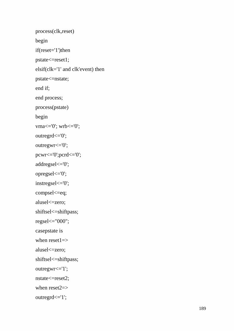
189
process(clk,reset)
begin
if(reset='1')then
pstate<=reset1;
elsif(clk='1' and clk'event) then
pstate<=nstate;
end if;
end process;
process(pstate)
begin
vma<='0'; wrb<='0';
outregrd<='0';
outregwr<='0';
pcwr<='0';pcrd<='0';
addregsel<='0';
opregsel<='0';
instregsel<='0';
compsel<=eq;
alusel<=zero;
shiftsel<=shiftpass;
regsel<="000";
casepstate is
when reset1=>
alusel<=zero;
shiftsel<=shiftpass;
outregwr<='1';
nstate<=reset2;
when reset2=>
outregrd<='1';

190
pcwr<='1';
addregsel<='1';
nstate<=reset3;
when reset3=>
vma<='1';
wrb<='0';
nstate<=reset4;
when reset4=>
if(ready='1')then
instregsel<='1';
nstate<=execute;
else
nstate<=reset3;
end if;
when execute=>
caseinstregout(15 downto 11) is
when "00000" =>
nstaTE<= MOV1;
when "00001" =>
nstate<=add1;
when "00010" =>
nstaTE<= mvi1;
when "00011" =>
nstaTE<= load1;
when others=>
null;
end case;
when add1=>
regsel<= instregout(5 downto 3);

191
regrd<= '1';
opregsel<= '1';
nstate<= add2;
when add2=>
regsel<=instregout(2 downto 0);
regrd<= '1';
alusel<= add;
shiftsel<= shiftpaSS;
outregwr<= '1';
nstate<= add3;
when add3=>
outregrd<= '1';
regsel<= instregout(2 downto 0);
regwr<= '1';
nstate<= incpc;
whenincpc=>
pcrd<= '1';
alusel<= inc;
shiftsel<= shiftpass;
outregwr<= '1';
nstaTE<= reset2;
when mov1=>
regsel<= instregout(5 downto 3);
regrd<= '1';
regsel<= instregout(2 downto 0);
regwr<= '1';
nstate<= incpc;
when mvi1=>
pcrd<= '1';

192
alusel<= inc;
shiftsel<= shiftpass;
outregwr<= '1';
nstate<= mvi2;
when mvi2=>
outregrd<= '1';
pcwr<= '1';
addregsel<= '1';
nstate<= mvi3;
when mvi3=>
vma<= '1';
wrb<='0';
nstate<= mvi4;
when mvi4=>
if(reaDY='1') then
regsel<= instregout(2 downto 0);
regwr<= '1';
nstate<= incpc;
else
nstate<= mvi3;
end if;
when load1=>
pcrd<= '1';
alusel<= inc;
shiftsel<= shiftpass;
outregwr<= '1';
nstate<= load2;
when load2=>
outregrd<= '1';

193
pcwr<= '1';
addregsel<= '1';
nstate<= load3;
when load3=>
vma<= '1';
wrb<= '0';
nstate<= load4;
when load4=>
if(ready='1')then
addregsel<='1';
nstate<= load5;
else
nstate<= load3;
end if;
when load5=>
vma<= '1';
wrb<= '0';
nstate<= load6;
when load6=>
if(ready='1')then
regsel<= instregout(2 downto 0);
regwr<= '1';
nstate<= incpc;
else
nstate<= load5;
end if;
end case;
end process;
end control;

194
SHIFT UNIT
--------------------------------------------------------------------------------------------
-------
--
-- Title : Event Processor for WSN node
-- Design : alu3
-- Author : ks
-- Company : mit
--
--------------------------------------------------------------------------------------------
-------
--
-- File : c:\My_Designs\check\alu3\compile\add0.vhd
-- Generated : Sun May 25 10:31:11 2008
-- From : c:\My_Designs\check\alu3\src\add0.bde
--
--------------------------------------------------------------------------------------------
-------
--
-- Description :
--
--------------------------------------------------------------------------------------------
-------
-- Design unit header --
library IEEE;
use IEEE.std_logic_1164.all;
packagemainpack is
typet_shift is (shl2,shr2,rol2,ror2,shiftpass);
subtypet_data is std_logic_vector(15 downto 0);

195
end package mainpack;
library IEEE;
usework.mainpack.all;
use IEEE.std_logic_1164.all;
entity shift is
port(a:int_data;
s:in t_shift;
y:out t_data);
end shift;
architecture shift of shift is
begin
process(a,s)
begin
case s is
when shl2=>
y<= a(14 downto 0) & '0';
when shr2=>
y<= '0' &a(15 downto 1);
when rol2=>
y<= a(14 downto 0) & a(15);
when ror2=>
y<= a(0) & a(15 downto 1);
whenshiftpass=>
y<=a;
end case;
end process;
end shift;
TRIREGISTER

196
--------------------------------------------------------------------------------------------
-------
--
-- Title : Event Processor for WSN node
-- Design : alu3
-- Author : ks
-- Company : mit
--
--------------------------------------------------------------------------------------------
-------
--
-- File : c:\My_Designs\check\alu3\compile\add0.vhd
-- Generated : Sun May 25 10:31:11 2008
-- From : c:\My_Designs\check\alu3\src\add0.bde
--
--------------------------------------------------------------------------------------------
-------
--
-- Description :
--
--------------------------------------------------------------------------------------------
-------
-- Design unit header --
libraryieee;
use ieee.std_logic_1164.all;
packagemainpack is
subtypet_data is std_logic_vector(15 downto 0);
end package mainpack;
library IEEE;

197
use IEEE.std_logic_1164.all;
usework.mainpack.all;
entitytrireg is
port (
a: in t_data;
rd: in STD_LOGIC;
wr: in STD_LOGIC;
y: out t_data );
endtrireg;
architecturetrigesi_arch of trireg is
begin
process(a,wr,rd)
variable u:std_logic_vector(15 downto 0);
begin
if(wr='1')then
u:=a;
elsif(rd='1')then
y<=u;
else
null;
end if;
end process;-- <<enter your statements here>>
endtrigesi_arch;
REGISTER ARRAY
--------------------------------------------------------------------------------------------
-------
--
-- Title : Event Processor for WSN node
-- Design : alu3

198
-- Author : ks
-- Company : mit
--
--------------------------------------------------------------------------------------------
-------
--
-- File : c:\My_Designs\check\alu3\compile\add0.vhd
-- Generated : Sun May 25 10:31:11 2008
-- From : c:\My_Designs\check\alu3\src\add0.bde
--
--------------------------------------------------------------------------------------------
-------
--
-- Description :
--
--------------------------------------------------------------------------------------------
-------
-- Design unit header --
libraryieee;
use ieee.std_logic_1164.all;
packagemainpack is
subtypet_data is std_logic_vector(15 downto 0);
subtypet_reg is std_logic_vector(2 downto 0);
end package mainpack;
library IEEE;
use IEEE.std_logic_1164.all;
usework.mainpack.all;
entityregarray is
port (
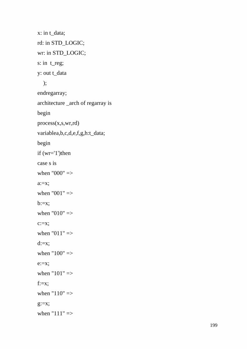
199
x: in t_data;
rd: in STD_LOGIC;
wr: in STD_LOGIC;
s: in t_reg;
y: out t_data
);
endregarray;
architecture _arch of regarray is
begin
process(x,s,wr,rd)
variablea,b,c,d,e,f,g,h:t_data;
begin
if (wr='1')then
case s is
when "000" =>
a:=x;
when "001" =>
b:=x;
when "010" =>
c:=x;
when "011" =>
d:=x;
when "100" =>
e:=x;
when "101" =>
f:=x;
when "110" =>
g:=x;
when "111" =>
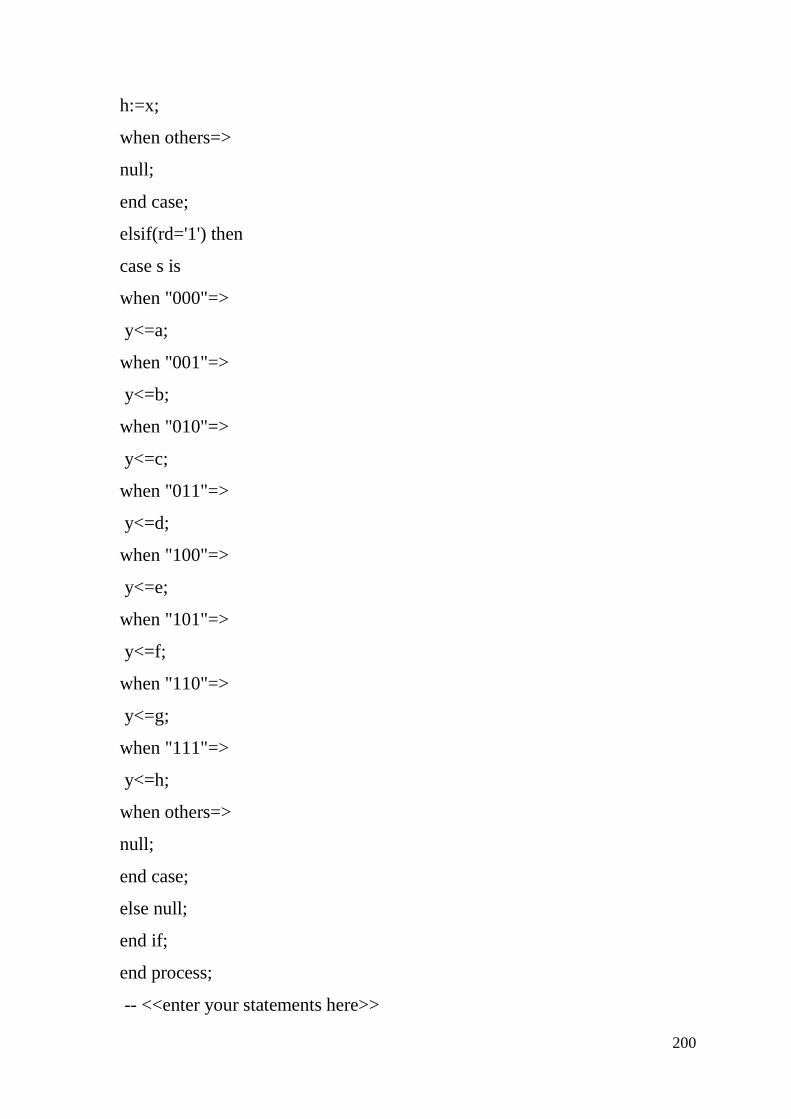
200
h:=x;
when others=>
null;
end case;
elsif(rd='1') then
case s is
when "000"=>
y<=a;
when "001"=>
y<=b;
when "010"=>
y<=c;
when "011"=>
y<=d;
when "100"=>
y<=e;
when "101"=>
y<=f;
when "110"=>
y<=g;
when "111"=>
y<=h;
when others=>
null;
end case;
else null;
end if;
end process;
-- <<enter your statements here>>

201
end arch;
RAM
--------------------------------------------------------------------------------------------
-------
--
-- Title : Event Processor for WSN node
-- Design : alu3
-- Author : ks
-- Company : mit
--
--------------------------------------------------------------------------------------------
-------
--
-- File : c:\My_Designs\check\alu3\compile\add0.vhd
-- Generated : Sun May 25 10:31:11 2008
-- From : c:\My_Designs\check\alu3\src\add0.bde
--
--------------------------------------------------------------------------------------------
-------
--
-- Description :
--
--------------------------------------------------------------------------------------------
-------
-- Design unit header --
libraryieee;
use ieee.std_logic_1164.all;
--library bitlib;
usework.bit_pack.all;

202
entitystatic_ram is
generic (
constanttaa :time := 120 ns;
constanttacs :time := 120 ns;
constanttclz :time := 10 ns;
constanttchz :time := 10 ns;
constanttoh :time := 10 ns;
constanttwc :time := 120 ns;
constant taw :time := 105 ns;
constanttwp :time := 70 ns;
constanttwhz :time := 35 ns;
constanttdw :time := 35 ns;
constanttdh :time := 0 ns;
constant tow :time := 10 ns
);
port (cs_b,we_b,oe_b :in bit;
address :in bit_vector(7 downto 0);
data :inoutstd_logic_vector(7 downto 0) := (others =>'Z')
);
endstatic_ram;
architecturesram of static_ram is
typeramtype is array(0 to 255) of bit_vector(7 downto 0);
signal ram1:ramtype;
signalflag:bit:='1';
begin
ram :process
begin
if flag='1' then
fori in 255 downto 0 loop
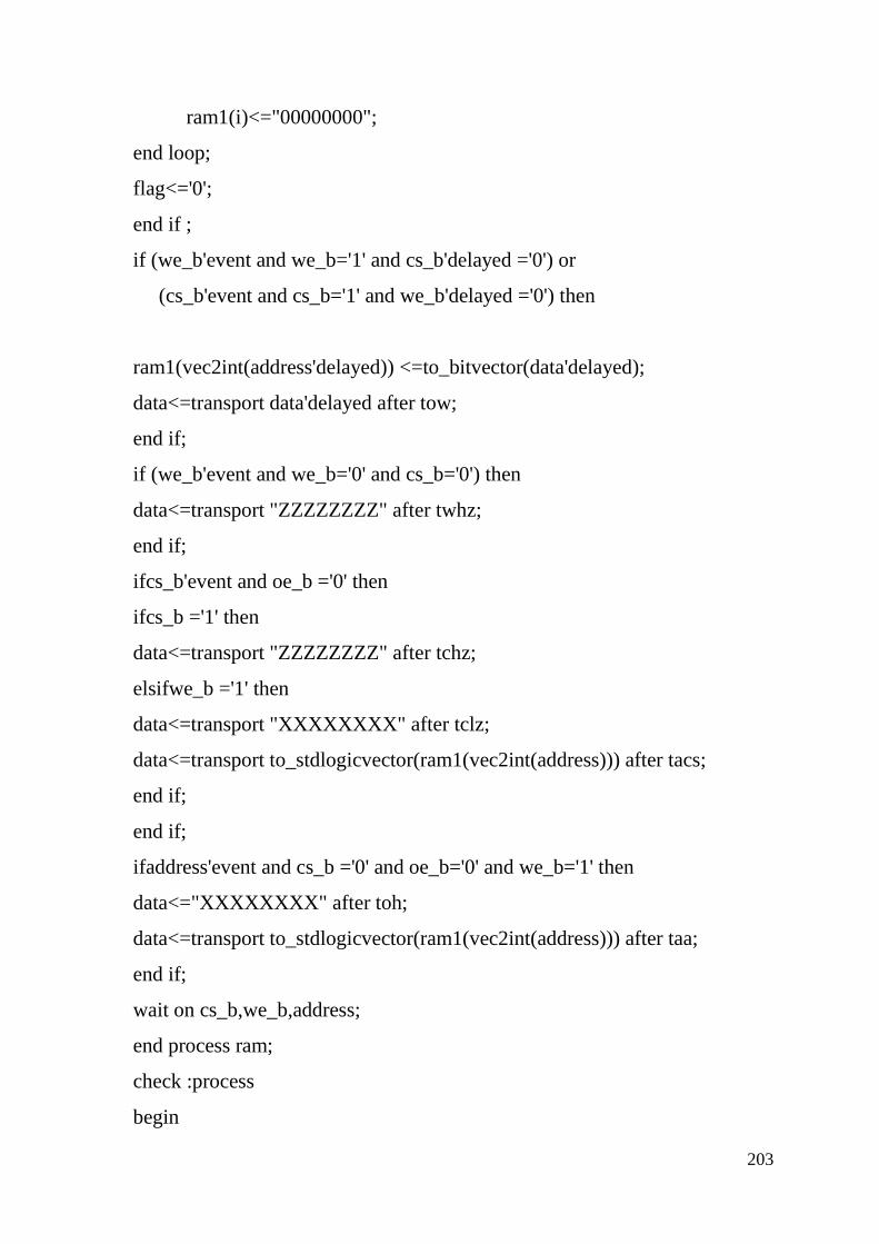
203
ram1(i)<="00000000";
end loop;
flag<='0';
end if ;
if (we_b'event and we_b='1' and cs_b'delayed ='0') or
(cs_b'event and cs_b='1' and we_b'delayed ='0') then
ram1(vec2int(address'delayed)) <=to_bitvector(data'delayed);
data<=transport data'delayed after tow;
end if;
if (we_b'event and we_b='0' and cs_b='0') then
data<=transport "ZZZZZZZZ" after twhz;
end if;
ifcs_b'event and oe_b ='0' then
ifcs_b ='1' then
data<=transport "ZZZZZZZZ" after tchz;
elsifwe_b ='1' then
data<=transport "XXXXXXXX" after tclz;
data<=transport to_stdlogicvector(ram1(vec2int(address))) after tacs;
end if;
end if;
ifaddress'event and cs_b ='0' and oe_b='0' and we_b='1' then
data<="XXXXXXXX" after toh;
data<=transport to_stdlogicvector(ram1(vec2int(address))) after taa;
end if;
wait on cs_b,we_b,address;
end process ram;
check :process
begin

204
ifcs_b'delayed='0' and now/=0 ns then
ifaddress'event then
assert (address'delayed'stable(twc))
report "address cycle time too short"
severity warning;
end if;
if (we_b'event and we_b='1') then
assert (address'delayed'stable(taw))
report "address not valid long enough to end of write"
severity warning;
assert (address'delayed'stable(twp))
report "write pluse too short"
severity warning;
assert (data'delayed'stable(tdw))
report "data setup time too short"
severity warning;
assert (data'last_event>=tdh)
report "address cycle time too short"
severity warning;
end if;
end if;
wait on we_b,address,cs_b;
end process check;
endsram;
ROM
--------------------------------------------------------------------------------------------
-------
--
-- Title : Event Processor for WSN node

205
-- Design :rom
-- Author : ks
-- Company : mit
--
--------------------------------------------------------------------------------------------
-------
--
-- File : c:\My_Designs\check\rom\compile\rom.vhd
-- Generated : Sun May 25 10:31:11 2008
-- From : c:\My_Designs\check\rom\src\rom.bde
--
--------------------------------------------------------------------------------------------
-------
--
-- Description : rom
--
--------------------------------------------------------------------------------------------
-------
-- Design unit header --
libraryieee;
use ieee.std_logic_1164.all;
useieee.std_logic_unsigned.all;
useieee.std_logic_arith.all;
entity rom16_8 is
port(addr:instd_logic_vector(3 downto 0);
ce:instd_logic;
dataout:outstd_logic_vector(7 downto 0)
);
end entity rom16_8;

206
architecture behave of rom16_8 is
begin
--10+20+60-10=80h
dataout<="00001001" when addr="0000" and ce='0' else --mov ax,9h
"00011010" when addr="0001" and ce='0' else --add ax,ah
"00011011" when addr="0010" and ce='0' else --add ax,bh
"00101100" when addr="0011" and ce='0' else --sub ax,ch
"11100000" when addr="0100" and ce='0' else --out
"11110000" when addr="0101" and ce='0' else --hlt
"00000000" when addr="0110" and ce='0' else
"00000000" when addr="0111" and ce='0' else
"00000000" when addr="1000" and ce='0' else
"00010000" when addr="1001" and ce='0' else --10h
"00100000" when addr="1010" and ce='0' else --20h
"01100000" when addr="1011" and ce='0' else --60h
"00010000" when addr="1100" and ce='0' else --10h
"00000000" when addr="1101" and ce='0' else
"00000000" when addr="1110" and ce='0' else
"00000000" when addr="1111" and ce='0' else
"11111111";
end architecture behave;
MAIN PROGRAM
--------------------------------------------------------------------------------------------
-------
--
-- Title : Event Processor for WSN node
-- Design : mprog
-- Author : ks
-- Company : mit
--
--------------------------------------------------------------------------------------------
-------
--
-- File : c:\My_Designs\check\mprog\compile\ mprog.vhd
-- Generated : Sun May 25 10:31:11 2008
-- From : c:\My_Designs\check\ mprog \src\ mprog.bde
--
--------------------------------------------------------------------------------------------
-------
--
-- Description :mprog
--

207
--------------------------------------------------------------------------------------------
-------
-- Design unit header --
libraryieee;
use ieee.std_logic_1164.all;
packagemainpack is
type t_alu is (add,sub,inc,dec,pass,zero,and2,or2,not2,nor2);
typet_shift is (shl2,shr2,rol2,ror2,shiftpass);
typet_comp is (eq,neq,gt,lt,gte,lte);
subtypet_data is std_logic_vector(15 downto 0);
subtypet_reg is std_logic_vector(2 downto 0);
type state is
(reset1,reset2,reset3,reset4,execute,add1,add2,add3,incpc,mov1,mvi1,mvi2,
mvi3,mvi4,load1,load2,load3,load4,load5,load6);
end package mainpack;
library IEEE;
use IEEE.std_logic_1164.all;
usework.mainpack.all;
entity mp is
port (
vma: out STD_LOGIC;
wrb: out STD_LOGIC;
clk: in STD_LOGIC;
reset: in STD_LOGIC;
ready: in STD_LOGIC;
address: out t_data;
data: inoutt_data
);
end mp;
architecturemp_arch of mp is
componentalu is
port(a,b:int_data;
s:in t_alu;
y:out t_data);
end component;
component shift is
port(a: in t_data;
s :in t_shift;
y:out t_data);
end component;
componentbireg is
port(a: in t_data;
s: in std_logic;

208
y:out t_data);
end component;
componenttrireg is
port( a: in t_data;
rd,wr:instd_logic;
y: out t_data);
end component;
component comp is
port(a,b: in t_data;
s:in t_comp;
y:out std_logic);
end component;
componentregarray is
port(X:int_data;
s:in t_reg;
rd,wr:in std_logic;
y:out t_data);
end component;
component control is
port(reset,ready,clk,compout:instd_logic;
instregout:int_data;
vma,wrb,outregwr,outregrd,regwr,regrd,pcrd,pcwr,addregsel,opregsel,instreg
sel:out std_logic;
compsel:outt_comp;
alusel:outt_alu;
shiftsel:outt_shift;
regsel:outt_reg
);
end component;
signal
compout,addregsel,opregsel,instregsel,pcwr,pcrd,regwr,regrd,outregwr,outre
grd:std_logic;
signalinstregout,aluout,shiftout,opregout:t_data;
signalshiftsel:t_shift;
signalalusel:t_alu;
signalregsel :t_reg;
signalcompsel:t_comp;
begin
u1: alu
port map(data,opregout,alusel,aluout);
u2:shift
port map(aluout,shiftsel,shiftout);

209
u3:comp
port map(data,opregout,compsel,compout);
u4:trireg -- outreg
port map(shiftout,outregrd,outregwr,data);
u5: trireg -- pc
port map(data,pcrd,pcwr,data);
u6:bireg -- addreg
port map(data,addregsel,address);
u7:bireg -- instrreg
port map(data,instregsel,instregout);
u8:bireg --- opreg
port map(data,opregsel,opregout);
u9: regarray
port map(data,regsel,regrd,regwr,data);
u10:control
port map(reset,ready,clk,compout,
instregout,
vma,wrb,outregwr,outregrd,regwr,regrd,pcrd,pcwr,addregsel,opregsel,instreg
sel,
compsel,
alusel,
shiftsel,
regsel);
-- <<enter your statements here>>
endmp_arch;

210
APPENDIX C:
Synthesis Reports

211
Synthesis Report of ALU
$ Start of Compile
Synplicity VHDL Compiler, version Compilers 2.6.0, Build 102R
Copyright (C) ,Synplicity Inc. All Rights Reserved
VHDL syntax check successful!
Synthesizing work.alu.rtl
Post processing for work.alu.rtl
@END
Process took 0h:0m:0srealtime, 0h:0m:0s cputime
###########################################################[
Synplicity Xilinx Technology Mapper, version 7.3.5, Build 222R
Copyright (C) ,Synplicity Inc. All Rights Reserved
Automatic dissolve during optimization of view:work.alu(rtl) of
un16_c_1(PM_ADDC__0_16)
Pass CPU time Worst Slack Luts / Registers
------------------------------------------------------------
------------------------------------------------------------
@N: FX164 |The option to pack flops in the IOB has not been specified
Writing Analyst data base C:\My_Designs\logic_controller\customizable
logic controller\synthesis\alu\alu.srm
Writing EDIF Netlist and constraint files
Writing VHDL Simulation files
@N: FC100 |Timing Report not generated for this device, please use place
and route tools for timing analysis.
---------------------------------------
Resource Usage Report for alu
Mapping to part: xc9572pc84-7
Simple gate primitives:
AND2 318 uses
AND2B1 117 uses
OR2 189 uses
XOR2 93 uses
I/O primitives: 52
IBUF 36 uses
OBUF 16 uses
I/O Register bits: 0
Register bits not including I/Os: 0
Mapper successful!
Process took 0h:0m:1srealtime, 0h:0m:1s cputime
###########################################################

212
Synthesis Report of Register Array
$ Start of Compile
Synplicity VHDL Compiler, version Compilers 2.6.0, Build 102R
Copyright (C) ,Synplicity Inc. All Rights Reserved
VHDL syntax check successful!
Synthesizing work.regarray.isha_arch
Post processing for work.regarray.isha_arch
@W: CL117
:"C:\My_Designs\new\con1\src\register_array.vhd":26:1:26:2|Latch
generated from process for signal y(15 downto 0), probably caused by a
missing assignment in an if or case stmt
@W: CL117
:"C:\My_Designs\new\con1\src\register_array.vhd":26:1:26:2|Latch
generated from process for signal g(15 downto 0), probably caused by a
missing assignment in an if or case stmt
@W: CL117
:"C:\My_Designs\new\con1\src\register_array.vhd":26:1:26:2|Latch
generated from process for signal f(15 downto 0), probably caused by a
missing assignment in an if or case stmt
@W: CL117
:"C:\My_Designs\new\con1\src\register_array.vhd":26:1:26:2|Latch
generated from process for signal e(15 downto 0), probably caused by a
missing assignment in an if or case stmt
@W: CL117
:"C:\My_Designs\new\con1\src\register_array.vhd":26:1:26:2|Latch
generated from process for signal d(15 downto 0), probably caused by a
missing assignment in an if or case stmt
@W: CL117
:"C:\My_Designs\new\con1\src\register_array.vhd":26:1:26:2|Latch
generated from process for signal c(15 downto 0), probably caused by a
missing assignment in an if or case stmt
@W: CL117
:"C:\My_Designs\new\con1\src\register_array.vhd":26:1:26:2|Latch
generated from process for signal b(15 downto 0), probably caused by a
missing assignment in an if or case stmt
@W: CL117
:"C:\My_Designs\new\con1\src\register_array.vhd":26:1:26:2|Latch
generated from process for signal a(15 downto 0), probably caused by a
missing assignment in an if or case stmt
@W: CL117
:"C:\My_Designs\new\con1\src\register_array.vhd":26:1:26:2|Latch

213
generated from process for signal h(15 downto 0), probably caused by a
missing assignment in an if or case stmt
@END
Process took 0h:0m:0srealtime, 0h:0m:0s cputime
###########################################################[
Synplicity Xilinx Technology Mapper, version 7.3.5, Build 222R
Copyright (C) ,Synplicity Inc. All Rights Reserved
Pass CPU time Worst Slack Luts / Registers
------------------------------------------------------------
------------------------------------------------------------
@N: FX164 |The option to pack flops in the IOB has not been specified
Writing Analyst data base
C:\My_Designs\new\con1\synthesis\regarray\regarray.srm
Writing EDIF Netlist and constraint files
Writing VHDL Simulation files
@N: FC100 |Timing Report not generated for this device, please use place
and route tools for timing analysis.
---------------------------------------
Resource Usage Report for regarray
Mapping to part: xc9572pc84-7
Simple gate primitives:
AND2 415 uses
AND2B1 112 uses
FDCP 144 uses
GND 1 use
OR2 112 uses
I/O primitives: 37
IBUF 21 uses
OBUF 16 uses
I/O Register bits: 0
Register bits not including I/Os: 144
Mapper successful!
Process took 0h:0m:0srealtime, 0h:0m:0s cputime
###########################################################]
Synthesis Report of Shift Unit
$ Start of Compile
Synplicity VHDL Compiler, version Compilers 2.6.0, Build 102R
Copyright (C) ,Synplicity Inc. All Rights Reserved
VHDL syntax check successful!
Synthesizing work.shift.shift

214
@N: CD231 :"C:\My_Designs\new\con1\src\shift_unit.vhd":5:13:5:14|Using
onehot encoding for type t_shift (shl2="10000")
Post processing for work.shift.shift
@END
Process took 0h:0m:0srealtime, 0h:0m:0s cputime
###########################################################[
Synplicity Xilinx Technology Mapper, version 7.3.5, Build 222R
Copyright (C) ,Synplicity Inc. All Rights Reserved
Pass CPU time Worst Slack Luts / Registers
------------------------------------------------------------
------------------------------------------------------------
@N: FX164 |The option to pack flops in the IOB has not been specified
Writing Analyst data base
C:\My_Designs\new\con1\synthesis\shift\shift.srm
Writing EDIF Netlist and constraint files
Writing VHDL Simulation files
@N: FC100 |Timing Report not generated for this device, please use place
and route tools for timing analysis.
---------------------------------------
Resource Usage Report for shift
Mapping to part: xc9572pc84-7
Simple gate primitives:
AND2 48 uses
OR2 34 uses
I/O primitives: 37
IBUF 21 uses
OBUF 16 uses
I/O Register bits: 0
Register bits not including I/Os: 0
Mapper successful!
Process took 0h:0m:0srealtime, 0h:0m:0s cputime
###########################################################]
Synthesis Report of Tri State Register
$ Start of Compile
Synplicity VHDL Compiler, version Compilers 2.6.0, Build 102R
Copyright (C) ,Synplicity Inc. All Rights Reserved
VHDL syntax check successful!
Synthesizing work.trireg.trigesi_arch
Post processing for work.trireg.trigesi_arch

215
@W: CL117 :"C:\My_Designs\new\con1\src\tri_reg.vhd":22:1:22:2|Latch
generated from process for signal y(15 downto 0), probably caused by a
missing assignment in an if or case stmt
@W: CL117 :"C:\My_Designs\new\con1\src\tri_reg.vhd":22:1:22:2|Latch
generated from process for signal u(15 downto 0), probably caused by a
missing assignment in an if or case stmt
@END
Process took 0h:0m:0srealtime, 0h:0m:0s cputime
###########################################################[
Synplicity Xilinx Technology Mapper, version 7.3.5, Build 222R
Copyright (C) ,Synplicity Inc. All Rights Reserved
Clock Buffers:
Inserting Clock buffer for port wr, TNM=wr
Pass CPU time Worst Slack Luts / Registers
------------------------------------------------------------
------------------------------------------------------------
@N: FX164 |The option to pack flops in the IOB has not been specified
Writing Analyst data base
C:\My_Designs\new\con1\synthesis\trireg\trireg.srm
Writing EDIF Netlist and constraint files
Writing VHDL Simulation files
@N: FC100 |Timing Report not generated for this device, please use place
and route tools for timing analysis.
---------------------------------------
Resource Usage Report for trireg
Mapping to part: xc9572pc84-7
Simple gate primitives:
AND2 65 uses
FDCP 32 uses
GND 1 use
I/O primitives: 33
IBUF 17 uses
OBUF 16 uses
BUFG 1 use
I/O Register bits: 0
Register bits not including I/Os: 32
Mapper successful!
Process took 0h:0m:0srealtime, 0h:0m:0s cputime
Synthesis Report of Bi-register
Start of Compile

216
Synplicity VHDL Compiler, version Compilers 2.6.0, Build 102R
Copyright (C) ,Synplicity Inc. All Rights Reserved
VHDL syntax check successful!
Synthesizing work.bireg.biregister_arch
Post processing for work.bireg.biregister_arch
@W: CL117
:"C:\My_Designs\new\con1\src\bi_register.vhd":22:0:22:1|Latch generated
from process for signal y(15 downto 0), probably caused by a missing
assignment in an if or case stmt
@END
Process took 0h:0m:0srealtime, 0h:0m:0s cputime
###########################################################[
Synplicity Xilinx Technology Mapper, version 7.3.5, Build 222R
Copyright (C) ,Synplicity Inc. All Rights Reserved
Clock Buffers:
Inserting Clock buffer for port s, TNM=s
Pass CPU time Worst Slack Luts / Registers
------------------------------------------------------------
------------------------------------------------------------
@N: FX164 |The option to pack flops in the IOB has not been specified
Writing Analyst data base
C:\My_Designs\new\con1\synthesis\bireg\bireg.srm
Writing EDIF Netlist and constraint files
Writing VHDL Simulation files
@N: FC100 |Timing Report not generated for this device, please use place
and route tools for timing analysis.
---------------------------------------Resource Usage Report for bireg
Mapping to part: xc9536pc44-5
Simple gate primitives:
AND2 32 uses
FDCP 16 uses
GND 1 use
I/O primitives: 32
IBUF 16 uses
OBUF 16 uses
BUFG 1 use
I/O Register bits: 0
Register bits not including I/Os: 16
Mapper successful!
Process took 0h:0m:0srealtime, 0h:0m:0s cputime
###########################################################]

217
Synthesis Report of Comparator
$ Start of Compile
Synplicity VHDL Compiler, version Compilers 2.6.0, Build 102R
Copyright (C) ,Synplicity Inc. All Rights Reserved
VHDL syntax check successful!
Synthesizing work.comp.comp
@N:CD231
:"C:\My_Designs\new\con1\src\comparator.vhd":4:12:4:13|Usingonehot
encoding for type t_comp (eq="100000")
Post processing for work.comp.comp
@END
Process took 0h:0m:0srealtime, 0h:0m:0s cputime
###########################################################[
Synplicity Xilinx Technology Mapper, version 7.3.5, Build 222R
Copyright (C) ,Synplicity Inc. All Rights Reserved
Pass CPU time Worst Slack Luts / Registers
------------------------------------------------------------
------------------------------------------------------------
@N: FX164 |The option to pack flops in the IOB has not been specified
Writing Analyst data base
C:\My_Designs\new\con1\synthesis\comp\comp.srm
Writing EDIF Netlist and constraint files
Writing VHDL Simulation files
@N: FC100 |Timing Report not generated for this device, please use place
and route tools for timing analysis.
---------------------------------------
Resource Usage Report for comp
Mapping to part: xc9536pc44-5
Simple gate primitives:
AND2 37 uses
AND2B1 32 uses
OR2 50 uses
XOR2 16 uses
I/O primitives: 39
IBUF 38 uses
OBUF 1 use
I/O Register bits: 0
Register bits not including I/Os: 0
Mapper successful!

218
Process took 0h:0m:0srealtime, 0h:0m:0s cputime
Synthesis Report of Control Unit
$ Start of Compile
Synplicity VHDL Compiler, version Compilers 2.6.0, Build 102R
Copyright (C) ,Synplicity Inc. All Rights Reserved
VHDL syntax check successful!
Synthesizing work.control.control
@N: CD231 :"C:\My_Designs\new\con1\src\control
unit.vhd":6:12:6:13|Using onehot encoding for type t_comp (eq="100000")
@N: CD231 :"C:\My_Designs\new\con1\src\control
unit.vhd":4:11:4:12|Using onehot encoding for type t_alu
(add="1000000000")
@N: CD231 :"C:\My_Designs\new\con1\src\control
unit.vhd":5:13:5:14|Using onehot encoding for type t_shift (shl2="10000")
@N: CD231 :"C:\My_Designs\new\con1\src\control
unit.vhd":9:11:9:12|Using onehot encoding for type state
(reset1="10000000000000000000")
@W: CG296 :"C:\My_Designs\new\con1\src\control
unit.vhd":39:0:39:6|Incomplete sensitivity list - assuming completeness
@W: CG290 :"C:\My_Designs\new\con1\src\control
unit.vhd":76:5:76:14|Referenced variable instregout is not in sensitivity list
@W: CG290 :"C:\My_Designs\new\con1\src\control
unit.vhd":53:5:53:10|Referenced variable ready is not in sensitivity list
Post processing for work.control.control
@W: CL117 :"C:\My_Designs\new\con1\src\control
unit.vhd":53:0:53:3|Latch generated from process for signal nstate(0 to 19),
probably caused by a missing assignment in an if or case stmt
@W: CL111 :"C:\My_Designs\new\con1\src\control unit.vhd":53:0:53:3|All
reachable assignments to regwr assign '1', register removed by optimization
@W:"C:\My_Designs\new\con1\src\control unit.vhd":53:0:53:3|All
reachable assignments to regwr assign 1, register removed by optimization
@W: CL117 :"C:\My_Designs\new\con1\src\control
unit.vhd":53:0:53:3|Latch generated from process for signal regrd, probably
caused by a missing assignment in an if or case stmt
@W: CL159 :"C:\My_Designs\new\con1\src\control
unit.vhd":16:21:16:27|Input compout is unused
@END
Process took 0h:0m:0srealtime, 0h:0m:0s cputime
###########################################################[
Synplicity Xilinx Technology Mapper, version 7.3.5, Build 222R

219
Copyright (C) ,Synplicity Inc. All Rights Reserved
@W:"c:\my_designs\new\con1\src\control unit.vhd":53:0:53:3|Sequential
instance nstate[19] has been reduced to a combinational gate by constant
propagation
Clock Buffers:
Inserting Clock buffer for port clk, TNM=clk
Pass CPU time Worst Slack Luts / Registers
------------------------------------------------------------
------------------------------------------------------------
@N: FX164 |The option to pack flops in the IOB has not been specified
Writing Analyst data base
C:\My_Designs\new\con1\synthesis\control\control.srm
Writing EDIF Netlist and constraint files
Writing VHDL Simulation files
@N: FC100 |Timing Report not generated for this device, please use place
and route tools for timing analysis.
---------------------------------------
Resource Usage Report for control
Mapping to part: xc9536pc44-5
Simple gate primitives:
AND2 76 uses
AND2B1 1 use
FDC 19 uses
FDCP 20 uses
FDP 1 use
GND 1 use
OR2 16 uses
VCC 1 use
XOR2 1 use
I/O primitives: 48
IBUF 13 uses
OBUF 35 uses
BUFG 1 use
I/O Register bits: 0
Register bits not including I/Os: 40
Mapper successful!
Process took 0h:0m:0srealtime, 0h:0m:0s cputime
###########################################################]
Synthesis Report of RAM
Synplicity VHDL Compiler, version Compilers 2.6.0, Build 102R
Copyright (C) ,Synplicity Inc. All Rights Reserved

220
VHDL syntax check successful!
Synthesizing work.ram.ram_arch
Post processing for work.ram.ram_arch
@W: CL169 :"C:\My_Designs\new1\logic
controller\src\ram.vhd":30:2:30:3|Pruning Register addrwr_temp_1(6
downto 0)
@N: CL134 :"C:\My_Designs\new1\logic
controller\src\ram.vhd":38:6:38:12|Found RAM ram_mem, depth=128,
width=8
@END
Process took 0h:0m:0srealtime, 0h:0m:0s cputime
###########################################################[
Synplicity Xilinx Technology Mapper, version 7.3.5, Build 222R
Copyright (C) ,Synplicity Inc. All Rights Reserved
@N: MF135 :"c:\my_designs\new1\logic
controller\src\ram.vhd":23:7:23:13|Found RAM, 'ram_mem[7:0]', 128 words
by 8 bits
Clock Buffers:
Inserting Clock buffer for port CLK, TNM=CLK
Pass CPU time Worst Slack Luts / Registers
------------------------------------------------------------
------------------------------------------------------------
@N: FX164 |The option to pack flops in the IOB has not been specified
Writing Analyst data base C:\My_Designs\new1\logic
controller\synthesis\ram\ram.srm
Writing EDIF Netlist and constraint files
Writing VHDL Simulation files
@N: FC100 |Timing Report not generated for this device, please use place
and route tools for timing analysis.
---------------------------------------
Resource Usage Report for ram
Mapping to part: xc9572pc84-7
Simple gate primitives:
AND2 2206 uses
AND2B1 2040 uses
FD 1024 uses
OR2 2040 uses
I/O primitives: 31
IBUF 23 uses
OBUF 8 uses
BUFG 1 use
I/O Register bits: 0
Register bits not including I/Os: 1024

221
Mapper successful!
Process took 0h:0m:12srealtime, 0h:0m:12scputime
###########################################################]
Synthesis Report of ROM
Synplicity VHDL Compiler, version Compilers 2.6.0, Build 102R
Copyright (C) ,Synplicity Inc. All Rights Reserved
VHDL syntax check successful!
Synthesizing work.rom.rom_arch
Post processing for work.rom.rom_arch
@W: CL169 :"C:\My_Designs\new1\logic
controller\src\rom.vhd":30:2:30:3|Pruning Register addrwr_temp_1(6
downto 0)
@N: CL134 :"C:\My_Designs\new1\logic
controller\src\rom.vhd":38:6:38:12|Found ROMrom_mem, depth=128,
width=8
@END
Process took 0h:0m:0srealtime, 0h:0m:0s cputime
###########################################################[
Synplicity Xilinx Technology Mapper, version 7.3.5, Build 222R
Copyright (C) ,Synplicity Inc. All Rights Reserved
@N: MF135 :"c:\my_designs\new1\logic
controller\src\rom.vhd":23:7:23:13|Found ROM, 'rom_mem[7:0]', 128 words
by 8 bits
Clock Buffers:
Inserting Clock buffer for port CLK, TNM=CLK
Pass CPU time Worst Slack Luts / Registers
------------------------------------------------------------
------------------------------------------------------------
@N: FX164 |The option to pack flops in the IOB has not been specified
Writing Analyst data base C:\My_Designs\new1\logic
controller\synthesis\rom\rom.srm
Writing EDIF Netlist and constraint files
Writing VHDL Simulation files
@N: FC100 |Timing Report not generated for this device, please use place
and route tools for timing analysis.
---------------------------------------
Resource Usage Report for rom
Mapping to part: xc9572pc84-7
Simple gate primitives:
AND2 2206 uses

222
AND2B1 2040 uses
FD 1024 uses
OR2 2040 uses
I/O primitives: 31
IBUF 23 uses
OBUF 8 uses
BUFG 1 use
I/O Register bits: 0
Register bits not including I/Os: 1024
Mapper successful!
Process took 0h:0m:12srealtime, 0h:0m:12scputime
###########################################################]
Synthesis Report of LATCH
$ Start of Compile
Synplicity VHDL Compiler, version Compilers 2.6.0, Build 102R
Copyright (C) ,Synplicity Inc. All Rights Reserved
VHDL syntax check successful!
Synthesizing work.latch.latch_arch
Post processing for work.latch.latch_arch
@W: CL117 :"C:\My_Designs\new1\logic
controller\src\latch.vhd":27:2:27:3|Latch generated from process for signal
temp_q(15 downto 0), probably caused by a missing assignment in an if or
case stmt
@END
Process took 0h:0m:0srealtime, 0h:0m:0s cputime
###########################################################[
Synplicity Xilinx Technology Mapper, version 7.3.5, Build 222R
Copyright (C) ,Synplicity Inc. All Rights Reserved
Pass CPU time Worst Slack Luts / Registers
------------------------------------------------------------
------------------------------------------------------------
@N: FX164 |The option to pack flops in the IOB has not been specified
Writing Analyst data base C:\My_Designs\new1\logic
controller\synthesis\latch\latch.srm
Writing EDIF Netlist and constraint files
Writing VHDL Simulation files
@N: FC100 |Timing Report not generated for this device, please use place
and route tools for timing analysis.
---------------------------------------
Resource Usage Report for latch
Mapping to part: xc9572pc84-7

223
Simple gate primitives:
AND2 33 uses
FDCP 16 uses
GND 1 use
OR2 32 uses
I/O primitives: 52
IBUF 20 uses
OBUF 32 uses
I/O Register bits: 0
Register bits not including I/Os: 16
Mapper successful!
Process took 0h:0m:0srealtime, 0h:0m:0s cputime
###########################################################]
224
APPENDIX D:
Microcontroller Code

225
Microcontroller (AT89S52) Assembly code
Delay: mov r0,#19h
mov @r0,#0bfh
inc r0
mov @r0,#86h
inc r0
mov @r0,#0dbh
inc r0
mov @r0,#0cfh
inc r0
mov @r0,#0e6h
inc r0 ; Storing the equivalent codes for display.
mov @r0,#0edh
inc r0
mov @r0,#fdh
inc r0
mov @r0,#87h
inc r0
mov @r0,#0ffh
inc r0
mov @r0,#0e7h
inc r0
mov @r0,#39h
inc r0
mov @r0,#00h
mov r0,#25h ; Storing the look up table
mov @r0,#40h
inc r0
mov @r0,#0f9h
inc r0
mov @r0,#24h
inc r0
mov @r0,#30h
inc r0
mov @r0,#99h
inc r0
mov @r0,#12h
inc r0
mov @r0,#02h
inc r0
mov @r0,#78h
inc r0
mov @r0,#00h
inc r0
mov @r0,#18h
inc r0
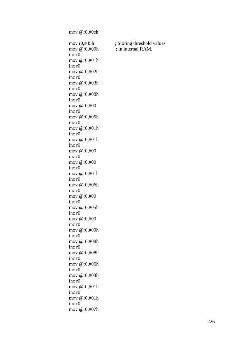
226
mov @r0,#0eh
mov r0,#45h ; Storing threshold values
mov @r0,#00h ; in internal RAM.
inc r0
mov @r0,#01h
inc r0
mov @r0,#02h
inc r0
mov @r0,#03h
inc r0
mov @r0,#08h
inc r0
mov @r0,#00
inc r0
mov @r0,#05h
inc r0
mov @r0,#01h
inc r0
mov @r0,#01h
inc r0
mov @r0,#00
inc r0
mov @r0,#00
inc r0
mov @r0,#01h
inc r0
mov @r0,#06h
inc r0
mov @r0,#00
inc r0
mov @r0,#05h
inc r0
mov @r0,#00
inc r0
mov @r0,#09h
inc r0
mov @r0,#08h
inc r0
mov @r0,#08h
inc r0
mov @r0,#06h
inc r0
mov @r0,#03h
inc r0
mov @r0,#01h
inc r0
mov @r0,#01h
inc r0
mov @r0,#07h

227
mov a,#08
STORE: dec a
inc r0
mov @r0,a
inc r0
movx @r0,a
inc r0
movx @r0,a
inc r0
movx @r0,a
djnz a,STORE
mov dptr,#2023h ; Configuring ports.
mov a,#81h
movx @dptr,a
mov dptr,#2043h
mov a,#80h
movx @dptr,a
mov r3,#00 ; Clears the display.
mov r4,#00
mov r5,#00
mov a,r5
call LED_CODES
mov dptr,#2040h
movx @dptr,a
inc dptr
movx @dptr,a
inc dptr
movx @dptr,a
mov dptr,#2022h
mov a,#30h
movx @dptr,a
mov sp,#11h
call lcdwel ; Calling LCD display subroutine.
REPEAT: clr psw.3
clr psw.4
mov dptr,#2022h
movx a,@dptr
cjne a,#31h,DONE ; Comparing whether humidity & temp
mov a,#0ah
xrl a,r4
jz DISPLAY ; Call delay.
call lcdbusy
mov a,#10h
movx @dptr,a ; check .
call DELAY
mov r7,#02
mov r6,#02h
call ADC
mov a,#0ah

228
xrl a,r3
jz I_FULL
inc r3
call DELAY
mov a,r3
call LOOK_UP_TABLE
mov dptr,#2042h
movx @dptr,a
mov r7,#02h
mov r6,#02h
call adc
mov dptr,#2022h
mov a,#30h
movx @dptr,a
call lcdwel
sjmp DONE
I_FULL: mov r7,#02h
mov r6,#02h
call ADC
inc r4
call DELAY
mov a,r4
call LOOK_UP_TABLE
mov dptr,#2041h
movx @dptr,a
mov r7,#04h
mov r6,#02h
call DELAY
mov dptr,#2022h
mov a,#30h
movx @dptr,a
call lcdwel
jmp DONE
DISPLAY: mov a,#70h
movx @dptr,a
GO: movx a,@dptr
jb a.0,GO
jmp OVER1
DONE: movx a,@dptr
cjne a,#33h,OVER1
mov a,#0ah
xrl a,r5
jz DISPLAY
mov a,#00
movx @dptr,a
call lcdbusy
setb psw.3
CLEAR: mov r1,#0ah
mov r0,#04h
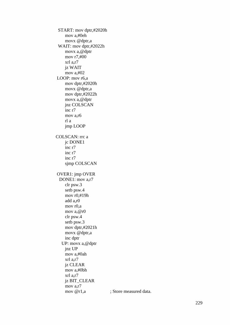
229
START: mov dptr,#2020h
mov a,#0eh
movx @dptr,a
WAIT: mov dptr,#2022h
movx a,@dptr
mov r7,#00
xrl a,r7
jz WAIT
mov a,#02
LOOP: mov r6,a
mov dptr,#2020h
movx @dptr,a
mov dptr,#2022h
movx a,@dptr
jnz COLSCAN
inc r7
mov a,r6
rl a
jmp LOOP
COLSCAN: rrc a
jc DONE1
inc r7
inc r7
inc r7
sjmp COLSCAN
OVER1: jmp OVER
DONE1: mov a,r7
clr psw.3
setb psw.4
mov r0,#19h
add a,r0
mov r0,a
mov a,@r0
clr psw.4
setb psw.3
mov dptr,#2021h
movx @dptr,a
inc dptr
UP: movx a,@dptr
jnz UP
mov a,#0ah
xrl a,r7
jz CLEAR
mov a,#0bh
xrl a,r7
jz BIT_CLEAR
mov a,r7
mov @r1,a ; Store measured data.

230
inc r1
mov r7,#0ffh
HEAR: djnz r7,HEAR
mov r7,#0ffh
HEAR1: djnz r7,HEAR1
djnz r0,START
mov r7,#0ah
mov r0,#45h
CHECK: mov r1,#0ah
mov r6,#03h
CHECK1:mov a,@r0
xrl a,@r1
jnz NEXT
inc r1
inc r0
djnz r6,CHECK1
mov dptr,#2022h
mov a,#90h
movx @dptr,a
clr psw.3
jmp OK
NEXT: inc r0
djnz r6,NEXT
inc r0
djnz r7,CHECK
mov dptr,#2022h
mov a,#50h
movx @dptr,a
AGAIN: movx a,@dptr
cjne a,#53h,AGAIN
clr psw.3
mov a,#30h
movx @dptr,a
REMAIN: movx a,@dptr
xrl a,#33h
jz REMAIN
mov r0,#0ffh
STAY: djnz r0,STAY
call lcdwel
jmp OVER
LED_CODES:setb psw.4
mov r0,#25h
add a,r0
mov r0,a
mov a,@r0
clr psw.4
ret

231
BIT_CLEAR: dec r1
inc r0
mov r6,#0ffh
HEAR2: djnz r6,HEAR2
mov r6,#0ffh
HEAR3: djnz r6,HEAR3
jmp START
OK: movx a,@dptr
cjne a,#91h,OK
mov a,#10h
movx @dptr,a
mov a,#00
mov dptr,#2021h
movx @dptr,a
call DELAY
mov r7,#06h
mov r6,#02h
call ADC
inc r5
call DELAY
mov a,r5
call LED_CODES
mov dptr,#2040h
movx @dptr,a
mov r7,#06h
mov r6,#02h
call DELAY
call lcdwel
jmp OVER
ADC:push r5
mov r5,#70h
mov r0,r6
mov dptr,#2020h
mov a,#88h
h3: movx @dptr,a
rl a
mov r2,#30
h1: mov r1,#255
h2: djnz r1,h2
djnz r2,h1
djnz r5,h3
mov r5,#0ffh
djnz r6,h3
mov r6,r0
djnz r7,h3
pop r5
ret

232
delay 8:push r5
mov r5,#70h
mov r0,r6
mov dptr,#2020h
mov a,#88h
h6: movx @dptr,a
rr a
mov r2,#30
h4: mov r1,#255
h5: djnz r1,h5
djnz r2,h4
djnz r5,h6
mov r5,#0ffh
djnz r6,h6
mov r6,r0
djnz r7,h6
pop r5
ret
DELAY: mov r1,#10h ; Subroutine for Delay
DELAY1: mov r2,#0ffh
DELAY2: mov r0,#0ffh
DELAY3: djnz r0,DELAY3
djnz r2,DELAY2
djnz r1,DELAY1
ret
OVER: mov dptr,#2022h
mov a,#30h
movx @dptr,a
movx a,@dptr
cjne a,#32h,I_OVER
mov a,#10h
movx @dptr,a
call lcdbusy
mov r7,#02h
mov r6,#02h
call MOTER_UP
dec r3
mov a,r3
call LED_CODES
mov dptr,#2042h
movx @dptr,a
call DELAY
mov r7,#02h
mov r6,#02h
call DELAY
mov dptr,#2022h
mov a,#30h
movx @dptr,a

233
call lcdwel
I_OVER: movx a,@dptr
cjne a,#34h,II_OVER
mov a,#10h
movx @dptr,a
call lcdbusy
mov r7,#04h
mov r6,#02h
call MOTER_UP
dec r4
mov a,r4
call LED_CODES
mov dptr,#2041h
movx @dptr,a
call DELAY
mov r7,#04h
mov r6,#02h
call MOTER_DOWN
mov dptr,#2022h
mov a,#30h
movx @dptr,a
call lcdwel
II_OVER: movx a,@dptr
cjne a,#38h,END
mov a,#10h
movx @dptr,a
call lcdbusy
mov r7,#06h
mov r6,#02h
call MOTER_UP
dec r5
mov a,r5
call LOOK_UP_TABLE
mov dptr,#2040h
movx @dptr,a
call DELAY
mov r7,#06h
mov r6,#02h
call MOTOR_DOWN ; Call delay
mov dptr,#2022h
mov a,#30h
movx @dptr,a
call lcdwel
END: jmp REPEAT
lcdwel: push r3 ; Subroutine for LCD to display
push r4
mov a,#3ch
call command
mov a,#0eh

234
call command
mov a,#01h
call command
mov a,#06h
call command
mov a,#80h
call command
mov a,#'W'
call data
mov a,#'E'
call data
mov a,#'L'
call data
mov a,#'C'
call data
mov a,#'O'
call data
mov a,#'M'
call data
mov a,#'E'
call data
mov a,#' '
call data
mov a,#88h
call command
mov a,#'T'
call data
mov a,#'O'
call data
mov a,#' '
call data
mov a,#'C'
call data
mov a,#'A'
call data1
mov a,#'R'
call data
mov a,#aah
call command
mov a,#'P'
call data
mov a,#'A'
call data
mov a,#'R'
call data
mov a,#'K'
call data
mov a,#'I'
call data
mov a,#'N'

235
call data
mov a,#'G'
call data
mov a,#' '
call data
mov a,#'S'
call data
mov a,#'Y'
call data
mov a,#'S'
call data
mov a,#'T'
call data
mov a,#'E'
call data
mov a,#'M'
call data
pop r4
pop r3
ret
command: mov p1,a
clr p3.4
setb p3.3
clr p3.3
mov r3,#50
A: mov r4,#255
R: djnz r4,R
djnz r3,A
ret
data: mov p1,a
setb p3.4
setb p3.3
clr p3.3
mov r3,#50
AAA: mov r4,#255
AA: djnz r4,AA
djnz r3,AAA
ret
lcdbusy: push r4 ; Subroutine for LCD to display
push r3
mov a,#3ch
call command
mov a,#0eh
call command
mov a,#01h
call command
mov a,#06h
call command

236
mov a,#80h
call command
mov a,#'L'
call data
mov a,#'I'
call data
mov a,#'F'
call data
mov a,#'T'
call data
mov a,#' '
call data
mov a,#' '
call data
mov a,#'I'
call data
mov a,#'S'
call data
mov a,#88h
call command
mov a,#' '
call data
mov a,#' '
call data
mov a,#'B'
call data
mov a,#'U'
call data
mov a,#'S'
call data
mov a,#'Y'
call data
mov a,#aah
call command
mov a,#'P'
call data
mov a,#'L'
call data
mov a,#'E'
call data
mov a,#'A'
call data
mov a,#'S'
call data
mov a,#'E'
call data
mov a,#' '
call data
mov a,#'W'
call data

237
mov a,#'A'
call data
mov a,#'I'
call data
mov a,#'T'
call data
mov a,#' '
call data
pop r3
pop r4
ret

238
APPENDIX E:
Biography

239
Biography
Kshitij Shinghal was born in Moradabad, India. He graduated with distinction with a
Bachelor of Technology in Electronics Engineering degree in June 1999 from Shivaji
University Kolhapur, India. He did his M. Tech. in Digital Communication from U.P.
Technical University, Lucknow in May 2006, under the guidance of Prof. J.P. Saini. He
joined Moradabad Institute of Technology, Moradabad in July 1999 as lecturer in
Electronics Engineering Department and is currently Associate Professor and Head of
Department of Electronics and communication engineering department. The college is a
NBA accredited, affiliated to U. P. Technical University, Lucknow, (India). His research
interests include Wireless Sensor Networks, Microprocessors, ASIC Design and
Verification. He has been in teaching for more than 12 years. He has more than 10
publications in various Referred International Journals like IJEST, IJWMN, IJAET,
IJCES, IJRTE, and MITIJEC and many more. Mr. Kshitij Shinghal reached by email at
[email protected] or by phone 09411874617.

240
APPENDIX F:
List of Reprints /
Publications
241
List of Reprints (attached) / Publications
Conferences: 05
[1] Kshitij Shinghal, Arti Noor, Neelam Srivastava, Raghuvir Singh (2009),
‘Design of Systems on a Chip: An Introduction’, National Conference on
Emerging Technologies, NCET-2009, January 24-25, 2009, pp. 112-114.
[2] Kshitij Shinghal, Arti Noor, Neelam Srivastava, Raghuvir Singh (2009),
‘The New Era of Wireless Sensor Network: A Survey’, National
Conference on Emerging Technologies, NCET-2009, January 24-
25,2009, pp. 144-147.
[3] Kshitij Shinghal, Arti Noor, Neelam Srivastava, Raghuvir Singh (2011),
“Energy Aware Transceiver for– Next Generation Wireless Sensor
Network Node”, International Conference on Advances in Electrical &
Electronics Engineering, ICAEEE-2011.
[4] Kshitij Shinghal, Arti Noor, Neelam Srivastava, Raghuvir Singh (2011),
‘Energy Aware WSN Node-For Agricultural Application, 2nd National
Conference on Global Trends and Innovations in Computer Application
& Informatics on 9-10 April, 2011, pp. 146-149.
[5] Kshitij Shinghal, Arti Noor, Neelam Srivastava, Raghuvir Singh (2011),
‘Energy Efficient WSN Node - For Agricultural Application’, National
Conference on VLSI Design & Embedded Systems (NCVDES-2011),
October 12-14, 2011, pp. 87-92.
Journal: 08
[6] Kshitij Shinghal, Arti Noor, Neelam Srivastava, Raghuvir Singh (2010),
“Wireless Sensor Networks in Agriculture: for potato farming”,

242
International Journal of Engineering Science and Technology (IJEST),
Vol. 2 Issue 8, pp.3955-3963.
[7] Kshitij Shinghal, Arti Noor, Neelam Srivastava, Raghuvir Singh (2011),
“Low Power pH Sensor for - Wireless Sensor Network Node Agricultural
Application”, International Journal of Advances in Engineering
&Technology (IJAET), Vol. 1, No. 3, pp-197-203.
[8] Kshitij Shinghal, Arti Noor, Neelam Srivastava, Raghuvir Singh (2011),
“Intelligent Humidity Sensor For - Wireless Sensor Network Agricultural
Application”, International Journal of Wireless & Mobile Networks
(IJWMN), Vol. 3, No. 1, pp- 118-128. DOI : 10.5121/ijwmn.2011.3111
[9] Kshitij Shinghal, Arti Noor, Neelam Srivastava, Raghuvir Singh (2011),
“Power Measurements of wireless sensor networks node”, International
Journal of Computer Engineering & Science (IJCES), Vol.1, Issue 1, pp
8-13.
[10] Kshitij Shinghal, Arti Noor, Neelam Srivastava, Raghuvir Singh
(2011), ‘A novel approach for Energy Management in Wireless Sensor
Networks Nodes’, MIT International Journal of Electronics and
Communication Engineering Vol. 1, No.2, pp. 91-96.
[11] Kshitij Shinghal, Arti Noor, Neelam Srivastava, Raghuvir Singh
(2011), ‘Custom Single Purpose Processor Design: For Low Power WSN
Node’, International Journal of Recent Trends in Electrical & Electronics
Engg. (IJRTE), Volume 1 Issue 1, pp. 15-24.
[12] Amit Sharma, Kshitij Shinghal, Neelam Srivastava (2012), ‘Design
and Performance Analysis of Energy Efficient Routing Algorithm for
Wireless Sensor Network’, International Journal of Engineering Research
and Applications (IJERA), Vol. 2, Issue 6, pp 816-821.

243
[13] Kshitij Shinghal, Arti Noor, Neelam Srivastava, Raghuvir Singh
(2013), ‘A New Paradigm of Energy Management for Wireless Sensor
Networks Node’, International Journal of Contemporary Research in
Engineering and Technology (accepted).

244
APPENDIX G:
Acceptance Letters/
Communications

245

246

247

248

249

250