Embed Size (px)
Citation preview
DE10-Lite
User Manual
1
www.terasic.com
September 7, 2016
DE10-Lite
User Manual
1
www.terasic.com
September 7, 2016
CONTENTS
Chapter 1 Introduction ..................................................................................................... 3
1. 1 Package Contents ............................................................................................................................ 3
1. 2 DE10-Lite System CD .................................................................................................................... 4
1. 3 Layout and Components ................................................................................................................. 4
1. 4 Block Diagram of the Board ........................................................................................................... 6
1. 5 Getting Help .................................................................................................................................... 7
Chapter 2 Control Panel ................................................................................................... 8
2. 1 Control Panel Setup ........................................................................................................................ 8
2. 2 Controlling the LEDs, 7-segment Displays................................................................................... 10
2. 3 Switches and Push-buttons ............................................................................................................ 12
2. 4 SDRAM Controller and Programmer ........................................................................................... 12
2. 5 Accelerometer ............................................................................................................................... 14
2. 6 VGA .............................................................................................................................................. 15
2. 7 Overall Structure of the DE10-Lite Control Panel ........................................................................ 16
Chapter 3 Using the Starter Kit ................................................................................... 17
3. 1 Configuration of MAX 10 FPGA on DE10-Lite ........................................................................... 17
3. 2 Clock Circuitry .............................................................................................................................. 24
3. 3 Using the Push-buttons, Switches and LEDs ................................................................................ 25
3. 4 Using the 7-segment Displays ....................................................................................................... 28
3. 5 Using 2x20 GPIO Expansion Headers .......................................................................................... 30
3. 6 Using Arduino Uno R3 Expansion Header ................................................................................... 32
3. 7 A/D Converter and Analog Input .................................................................................................. 34
3. 8 Using VGA ................................................................................................................................... 35
3. 9 Using SDRAM .............................................................................................................................. 37
3. 10 Using Accelerometer Sensor ......................................................................................................... 39
Chapter 4 DE10-Lite System Builder ............................................................................ 41
4. 1 Introduction ................................................................................................................................... 41
4. 2 General Design Flow .................................................................................................................... 42
DE10-Lite
User Manual
2
www.terasic.com
September 7, 2016
4. 3 Using DE10-Lite System Builder ................................................................................................. 43
Chapter 5 Examples of Advanced Demonstrations .................................................... 48
5. 1 DE10-Lite Factory Configuration ................................................................................................. 48
5. 2 SDRAM Test in Nios II ................................................................................................................. 50
5. 3 SDRAM Test in Verilog ................................................................................................................ 53
5. 4 VGA Pattern .................................................................................................................................. 55
5. 5 G-Sensor ........................................................................................................................................ 57
5. 6 ADC Measurement ....................................................................................................................... 59
DE10-Lite
User Manual
3
www.terasic.com
September 7, 2016
Chapter 1
Introduction
The DE10-Lite presents a robust hardware design platform built around the Altera MAX 10 FPGA.
The MAX 10 FPGA is well equipped to provide cost effective, single-chip solutions in control
plane or data path applications and industry-leading programmable logic for ultimate design
flexibility. With MAX 10 FPGA, you can get lower power consumption / cost and higher
performance. When you need high-volume applications, including protocol bridging, motor control
drive, analog to digital conversion, image processing, and handheld devices, the MAX 10 Lite
FPGA is your best choice.
The DE10-Lite development board includes hardware such as on-board USB Blaster, 3-axis
accelerometer, video capabilities and much more. By leveraging all of these capabilities, the
DE10-Lite is the perfect solution for showcasing, evaluating, and prototyping the true potential of
the Altera MAX 10 FPGA.
The DE10-Lite contains all components needed to use the board in conjunction with a computer
that runs the Microsoft Windows XP or later.
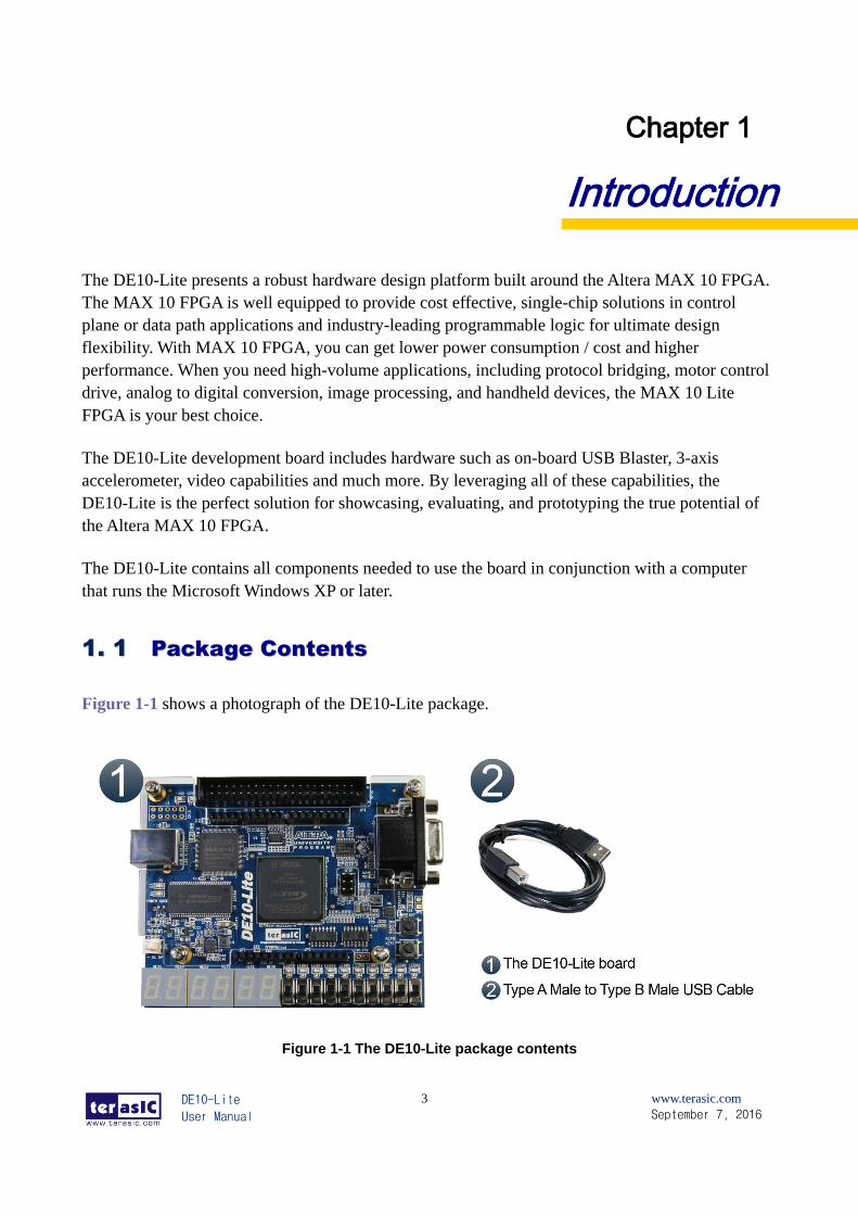
11.. 11 PPaacckkaaggee CCoonntteennttss
Figure 1-1 shows a photograph of the DE10-Lite package.
Figure 1-1 The DE10-Lite package contents
DE10-Lite
User Manual
4
www.terasic.com
September 7, 2016
The DE10-Lite package includes:
The DE10-Lite board
Type A Male to Type B Male USB Cable
11.. 22 DDEE1100--LLiittee SSyysstteemm CCDD
The DE10-Lite System CD contains the documentation and supporting materials, including the
User Manual, Control Panel, System Builder, reference designs and device datasheets.
User can download this System CD from the web (http://DE10-Lite.terasic.com/cd).
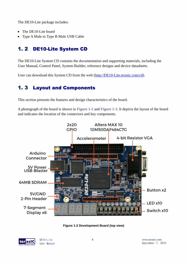
11.. 33 LLaayyoouutt aanndd CCoommppoonneennttss
This section presents the features and design characteristics of the board.
A photograph of the board is shown in Figure 1-2 and Figure 1-3. It depicts the layout of the board
and indicates the location of the connectors and key components.
Figure 1-2 Development Board (top view)

DE10-Lite
User Manual
5
www.terasic.com
September 7, 2016
Figure 1-3 Development Board (bottom view)
This board has many features that allow users to implement a wide range of designed circuits, from
simple circuits to various multimedia projects.
The following hardware is provided on the board:
FFPPGGAA DDeevviiccee
MAX 10 10M50DAF484C7G Device
Integrated dual ADCs, each ADC supports 1 dedicated analog input and 8 dual function pins
50K programmable logic elements
1,638 Kbit M9K Memory
5,888 Kbits user flash memory
144 18 × 18 Multiplier
4 PLLs
PPrrooggrraammmmiinngg aanndd CCoonnffiigguurraattiioonn
On-Board USB Blaster (Normal type B USB connector)
MMeemmoorryy DDeevviiccee
64MB SDRAM, x16 bits data bus
DE10-Lite
User Manual
6
www.terasic.com
September 7, 2016
CCoonnnneeccttoorrss
2x20 GPIO Header
Arduino Uno R3 Connector, including six ADC channels.
DDiissppllaayy
4-bit resistor-network DAC for VGA (With 15-pin high-density D-sub connector)
SSwwiittcchheess,, BBuuttttoonnss aanndd LLEEDDss
10 LEDs
10 Slide Switches
2 Push Buttons with Debounced.
Six 7-Segments
PPoowweerr
5V DC input from USB or external power connector.
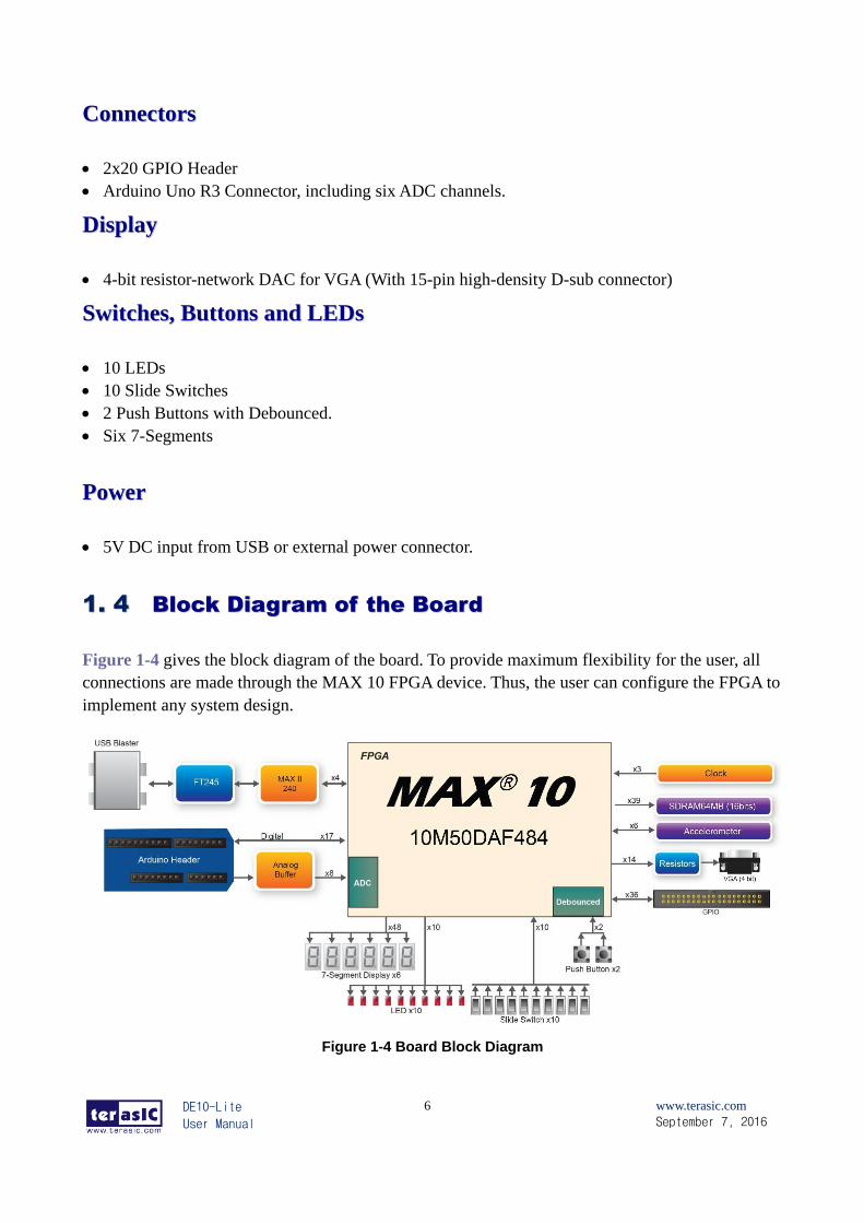
11.. 44 BBlloocckk DDiiaaggrraamm ooff tthhee BBooaarrdd
Figure 1-4 gives the block diagram of the board. To provide maximum flexibility for the user, all
connections are made through the MAX 10 FPGA device. Thus, the user can configure the FPGA to
implement any system design.
Figure 1-4 Board Block Diagram
DE10-Lite
User Manual
7
www.terasic.com
September 7, 2016
11.. 55 GGeettttiinngg HHeellpp
Here are the addresses where you can get help if you encounter any problem:
Terasic Inc.
9F., No.176, Sec.2, Gongdao 5th Rd, East Dist, Hsinchu City, 30070. Taiwan
Email: [email protected]
Tel.: +886-3-5750-880
Web: http://DE10-Lite.terasic.com
DE10-Lite
User Manual
8
www.terasic.com
September 7, 2016
Chapter 2
Control Panel
The DE10-Lite board comes with a Control Panel program that allows users to access various
components on the board from a host computer. The host computer communicates with the board
through a USB connection. The program can be used to verify the functionality of components on
the board or be used as a debug tool while developing any RTL code.
This chapter first presents some basic functions of the Control Panel, then describes its structure in
the block diagram form, and finally describes its capabilities.
22.. 11 CCoonnttrrooll PPaanneell SSeettuupp
The Control Panel Software Utility is located in the directory “Tools/ControlPanel” in the
DE10-Lite System CD. It's free of installation, just copy the whole folder to your host computer
and launch the control panel by executing the “DE10_Lite_ControlPanel.exe”.
Specific control circuits should be downloaded to your FPGA board before the control panel can
request it to perform required tasks. The program will call Quartus II tools to download the control
circuit to the FPGA board through the USB-Blaster[USB-0] connection.
To activate the Control Panel, perform the following steps:
1. Make sure Quartus II 16.0 or a later version is installed successfully on your PC.
2. Connect the USB cable provided to the USB Blaster port.
3. Start the executable DE10_Lite_ControlPanel.exe on the host computer. The Control Panel user
interface shown in Figure 2-1 will appear.
4. The DE10_Lite_ControlPanel.sof bit stream is loaded automatically as soon as the
DE10_Lite_ControlPanel.exe is launched.
5. In case of a disconnect, click on CONNECT where the .sof will be re-loaded onto the board.
Please note that the Control Panel will occupy the USB port until you close that port; you cannot use Quartus II
to download a configuration file into the FPGA until the USB port is closed.

DE10-Lite
User Manual
9
www.terasic.com
September 7, 2016
6. The Control Panel is now ready to use; experience it by setting the ON/OFF status for some
LEDs and observing the result on the DE10-Lite board.
Figure 2-1 The DE10-Lite Control Panel
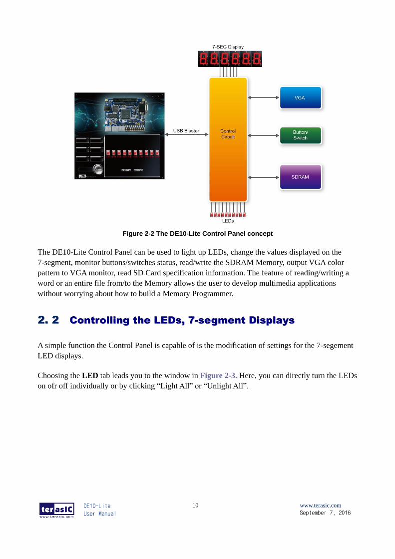
The concept of the DE1-Lite Control Panel is illustrated in Figure 2-2. The “Control Circuit” that
performs the control functions is implemented in the FPGA board. It communicates with the
Control Panel window, which is active on the host computer, via the USB Blaster link. The
graphical interface is used to send commands to the control circuit. It handles all the requests and
performs data transfers between the computer and the DE10-Lite board.
DE10-Lite
User Manual
10
www.terasic.com
September 7, 2016
Figure 2-2 The DE10-Lite Control Panel concept
The DE10-Lite Control Panel can be used to light up LEDs, change the values displayed on the
7-segment, monitor buttons/switches status, read/write the SDRAM Memory, output VGA color
pattern to VGA monitor, read SD Card specification information. The feature of reading/writing a
word or an entire file from/to the Memory allows the user to develop multimedia applications
without worrying about how to build a Memory Programmer.
22.. 22 CCoonnttrroolllliinngg tthhee LLEEDDss,, 77--sseeggmmeenntt DDiissppllaayyss
A simple function the Control Panel is capable of is the modification of settings for the 7-segement
LED displays.
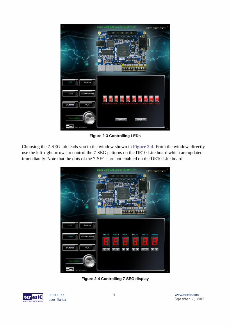
Choosing the LED tab leads you to the window in Figure 2-3. Here, you can directly turn the LEDs
on ofr off individually or by clicking “Light All” or “Unlight All”.
DE10-Lite
User Manual
11
www.terasic.com
September 7, 2016
Figure 2-3 Controlling LEDs
Choosing the 7-SEG tab leads you to the window shown in Figure 2-4. From the window, directly
use the left-right arrows to control the 7-SEG patterns on the DE10-Lite board which are updated
immediately. Note that the dots of the 7-SEGs are not enabled on the DE10-Lite board.
Figure 2-4 Controlling 7-SEG display
DE10-Lite
User Manual
12
www.terasic.com
September 7, 2016
The ability to set arbitrary values into simple display devices is not needed in typical design
activities. However, it gives users a simple mechanism for verifying that these devices are
functioning correctly in case a malfunction is suspected. Thus, it can be used for troubleshooting
purposes.
22.. 33 SSwwiittcchheess aanndd PPuusshh--bbuuttttoonnss
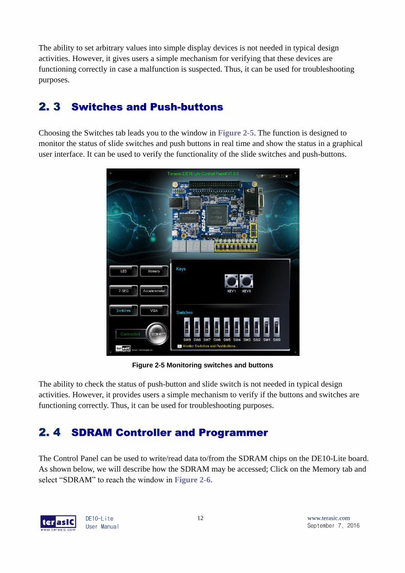
Choosing the Switches tab leads you to the window in Figure 2-5. The function is designed to
monitor the status of slide switches and push buttons in real time and show the status in a graphical
user interface. It can be used to verify the functionality of the slide switches and push-buttons.
Figure 2-5 Monitoring switches and buttons
The ability to check the status of push-button and slide switch is not needed in typical design
activities. However, it provides users a simple mechanism to verify if the buttons and switches are
functioning correctly. Thus, it can be used for troubleshooting purposes.
22.. 44 SSDDRRAAMM CCoonnttrroolllleerr aanndd PPrrooggrraammmmeerr
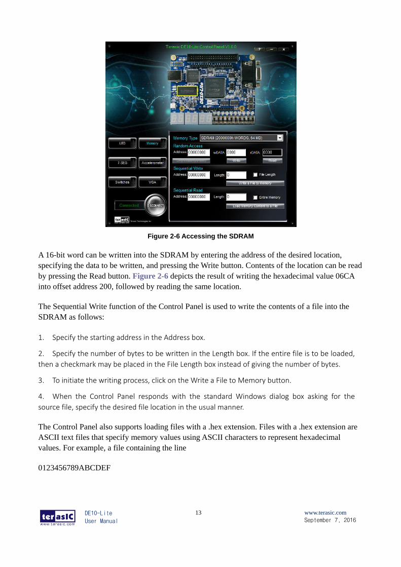
The Control Panel can be used to write/read data to/from the SDRAM chips on the DE10-Lite board.
As shown below, we will describe how the SDRAM may be accessed; Click on the Memory tab and
select “SDRAM” to reach the window in Figure 2-6.
DE10-Lite
User Manual
13
www.terasic.com
September 7, 2016
Figure 2-6 Accessing the SDRAM
A 16-bit word can be written into the SDRAM by entering the address of the desired location,
specifying the data to be written, and pressing the Write button. Contents of the location can be read
by pressing the Read button. Figure 2-6 depicts the result of writing the hexadecimal value 06CA
into offset address 200, followed by reading the same location.
The Sequential Write function of the Control Panel is used to write the contents of a file into the
SDRAM as follows:
1. Specify the starting address in the Address box.
2. Specify the number of bytes to be written in the Length box. If the entire file is to be loaded,
then a checkmark may be placed in the File Length box instead of giving the number of bytes.
3. To initiate the writing process, click on the Write a File to Memory button.
4. When the Control Panel responds with the standard Windows dialog box asking for the
source file, specify the desired file location in the usual manner.
The Control Panel also supports loading files with a .hex extension. Files with a .hex extension are
ASCII text files that specify memory values using ASCII characters to represent hexadecimal
values. For example, a file containing the line
0123456789ABCDEF
DE10-Lite
User Manual
14
www.terasic.com
September 7, 2016
defines eight 8-bit values: 01, 23, 45, 67, 89, AB, CD, EF. These values will be loaded
consecutively into the memory.
The Sequential Read function is used to read the contents of the SDRAM and fill them into a file as
follows:
1. Specify the starting address in the Address box.
2. Specify the number of bytes to be copied into the file in the Length box. If the entire contents
of the SDRAM are to be copied (which involves all 64 Mbytes), then place a checkmark in the
Entire Memory box.
3. Press Load Memory Content to a File button.
4. When the Control Panel responds with the standard Windows dialog box asking for the
destination file, specify the desired file in the usual manner.
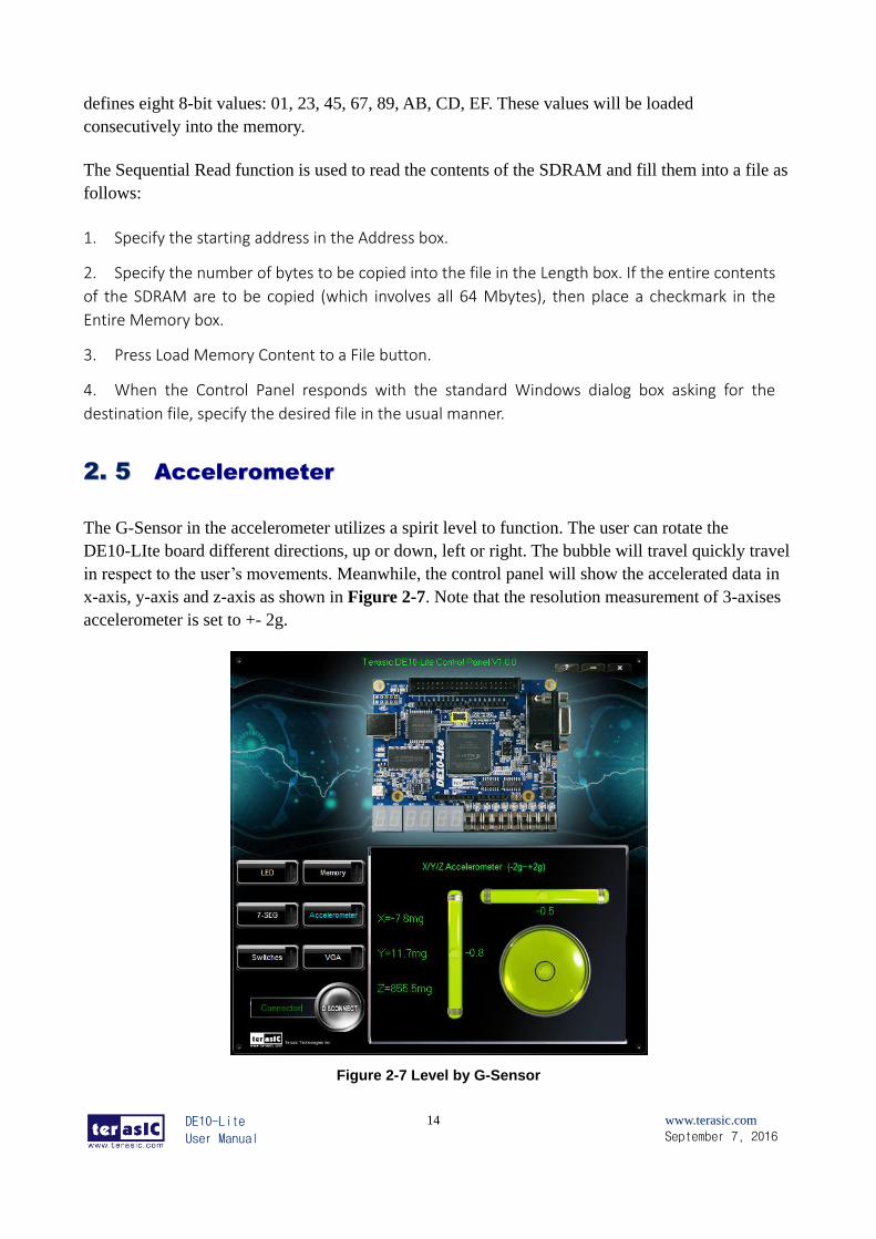
22.. 55 AAcccceelleerroommeetteerr
The G-Sensor in the accelerometer utilizes a spirit level to function. The user can rotate the
DE10-LIte board different directions, up or down, left or right. The bubble will travel quickly travel
in respect to the user’s movements. Meanwhile, the control panel will show the accelerated data in
x-axis, y-axis and z-axis as shown in Figure 2-7. Note that the resolution measurement of 3-axises
accelerometer is set to +- 2g.
Figure 2-7 Level by G-Sensor

DE10-Lite
User Manual
15
www.terasic.com
September 7, 2016
22.. 66 VVGGAA
DE10-Lite Control Panel provides VGA pattern function that allows users to output color pattern to
LCD/CRT monitor using the DE10-Lite board. Follow the steps below to generate the VGA pattern
function:
Choosing the VGA tab leads you to the window in Figure 2-8.
Plug a D-sub cable to the VGA connector of the DE10-Lite board and LCD /CRT monitor.
The LCD/CRT monitor will display the same color pattern on the control panel window.
Click the drop down menu shown in Figure 2-8 where you can output the selected pattern
individually.
Figure 2-8 Controlling VGA display under Control Panel
DE10-Lite
User Manual
16
www.terasic.com
September 7, 2016
22.. 77 OOvveerraallll SSttrruuccttuurree ooff tthhee DDEE1100--LLiittee CCoonnttrrooll PPaanneell
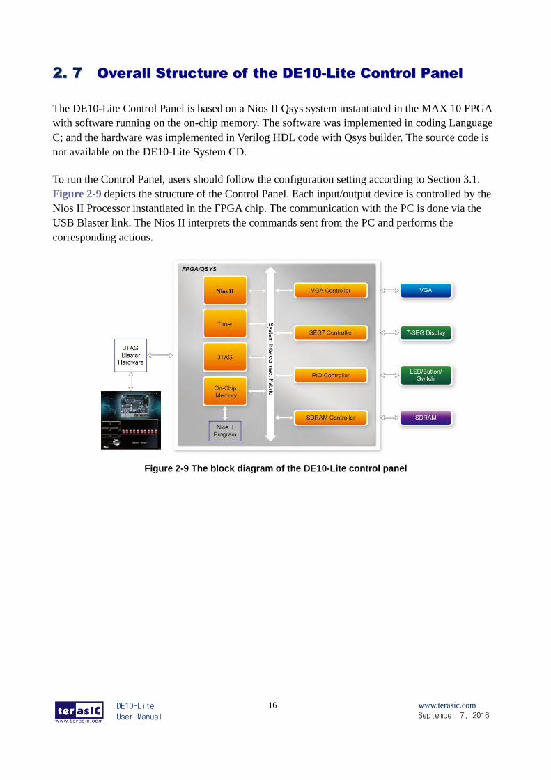
The DE10-Lite Control Panel is based on a Nios II Qsys system instantiated in the MAX 10 FPGA
with software running on the on-chip memory. The software was implemented in coding Language
C; and the hardware was implemented in Verilog HDL code with Qsys builder. The source code is
not available on the DE10-Lite System CD.
To run the Control Panel, users should follow the configuration setting according to Section 3.1.
Figure 2-9 depicts the structure of the Control Panel. Each input/output device is controlled by the
Nios II Processor instantiated in the FPGA chip. The communication with the PC is done via the
USB Blaster link. The Nios II interprets the commands sent from the PC and performs the
corresponding actions.
Figure 2-9 The block diagram of the DE10-Lite control panel
DE10-Lite
User Manual
17
www.terasic.com
September 7, 2016
Chapter 3
Using the Starter Kit
This chapter provides instructions to use the board and describes the peripherals.
33.. 11 CCoonnffiigguurraattiioonn ooff MMAAXX 1100 FFPPGGAA oonn DDEE1100--LLiittee
There are two types of configuration method supported by DE10-Lite:
1. JTAG configuration: configuration using JTAG ports.
JTAG configuration scheme allows you to directly configure the device core through JTAG pins -
TDI, TDO, TMS, and TCK pins. The Quartus II software automatically generates .sof files that are
used for JTAG configuration with a download cable in the Quartus II software program.
2. Internal configuration: configuration using internal flash.
Before internal configuration, you need to program the configuration data into the configuration
flash memory (CFM) which provides non-volatile storage for the bit stream. The information is
retained within CFM even if the DE10-Lite board is turned off. When the board is powered on, the
configuration data in the CFM is automatically loaded into the MAX 10 FPGA.
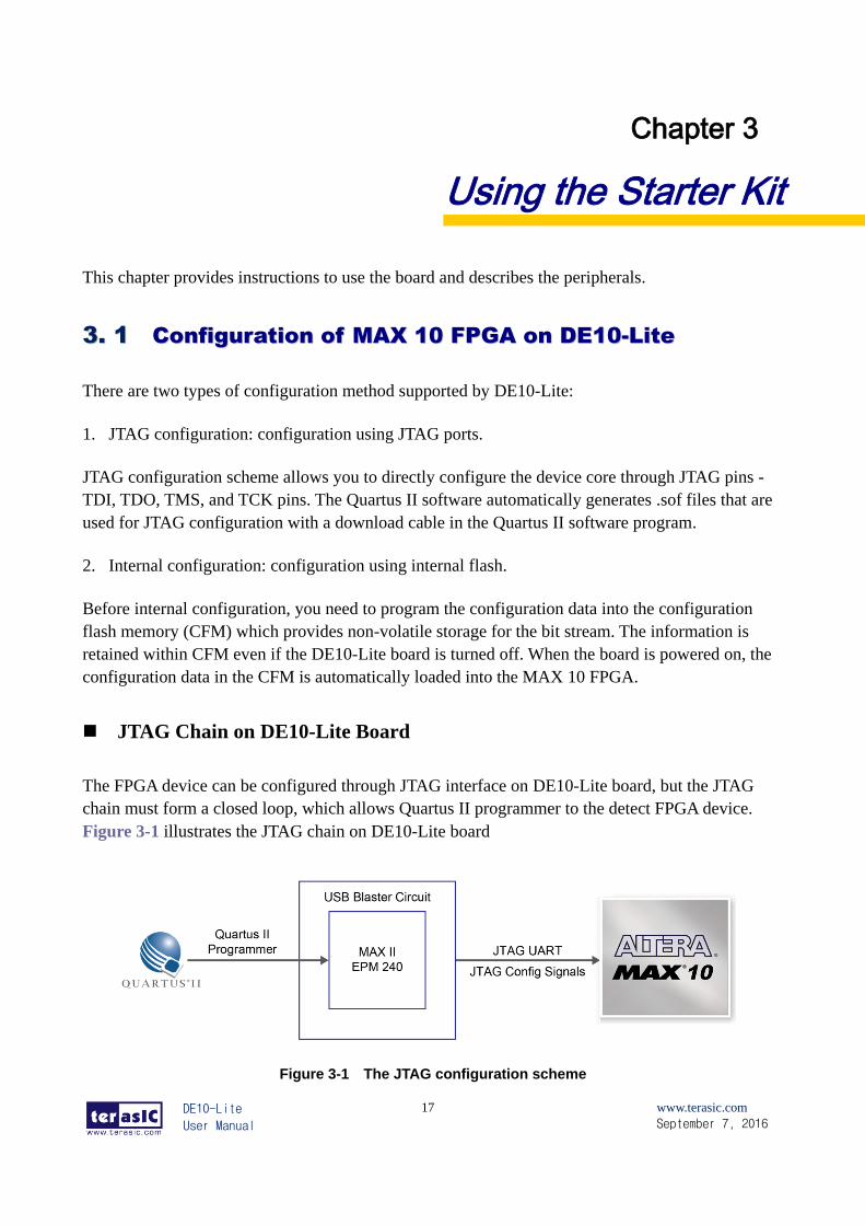
JTAG Chain on DE10-Lite Board
The FPGA device can be configured through JTAG interface on DE10-Lite board, but the JTAG
chain must form a closed loop, which allows Quartus II programmer to the detect FPGA device.
Figure 3-1 illustrates the JTAG chain on DE10-Lite board
Figure 3-1 The JTAG configuration scheme
DE10-Lite
User Manual
18
www.terasic.com
September 7, 2016
Configure the FPGA in JTAG Mode
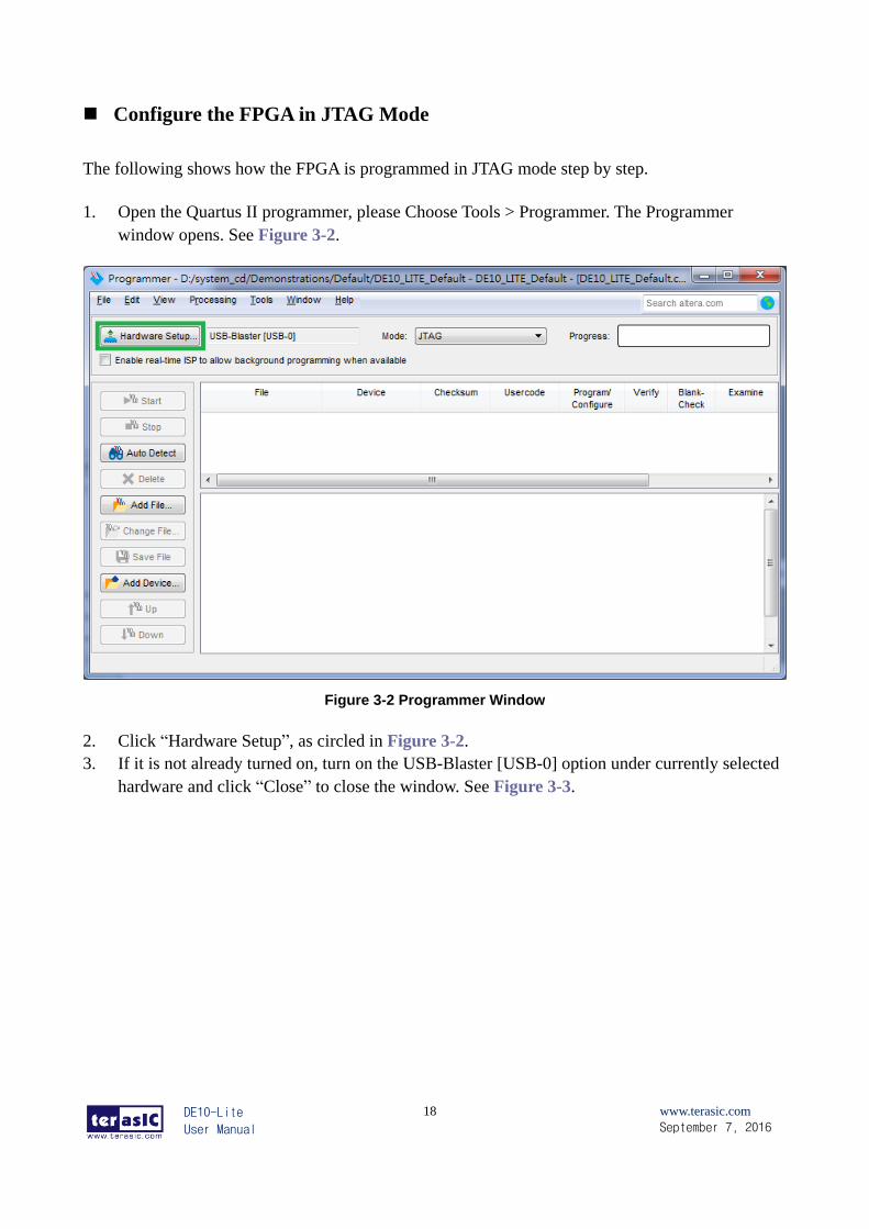
The following shows how the FPGA is programmed in JTAG mode step by step.
1. Open the Quartus II programmer, please Choose Tools > Programmer. The Programmer
window opens. See Figure 3-2.
Figure 3-2 Programmer Window
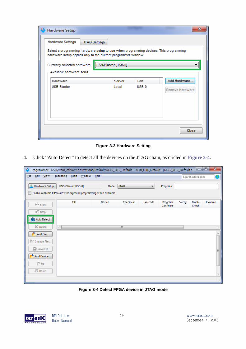
2. Click “Hardware Setup”, as circled in Figure 3-2.
3. If it is not already turned on, turn on the USB-Blaster [USB-0] option under currently selected
hardware and click “Close” to close the window. See Figure 3-3.
DE10-Lite
User Manual
19
www.terasic.com
September 7, 2016
Figure 3-3 Hardware Setting
4. Click “Auto Detect” to detect all the devices on the JTAG chain, as circled in Figure 3-4.
Figure 3-4 Detect FPGA device in JTAG mode

DE10-Lite
User Manual
20
www.terasic.com
September 7, 2016
5. Select detected device associated with the board, as circled in Figure 3-5.
x
Figure 3-5 Select 10M50DA device
6. FPGA is detected, as shown in Figure 3-6.
Figure 3-6 FPGA detected in Quartus II programmer
DE10-Lite
User Manual
21
www.terasic.com
September 7, 2016
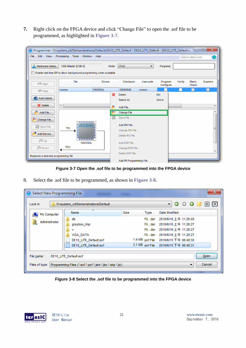
7. Right click on the FPGA device and click “Change File” to open the .sof file to be
programmed, as highlighted in Figure 3-7.
Figure 3-7 Open the .sof file to be programmed into the FPGA device
8. Select the .sof file to be programmed, as shown in Figure 3-8.
Figure 3-8 Select the .sof file to be programmed into the FPGA device
DE10-Lite
User Manual
22
www.terasic.com
September 7, 2016
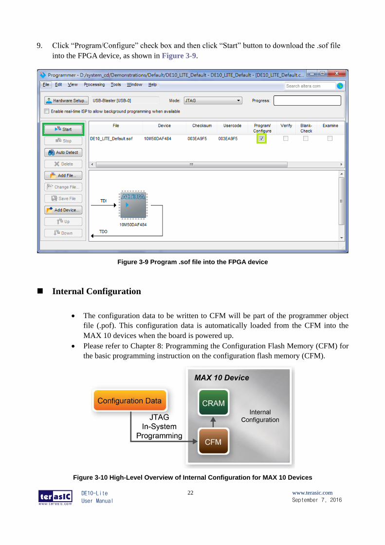
9. Click “Program/Configure” check box and then click “Start” button to download the .sof file
into the FPGA device, as shown in Figure 3-9.
Figure 3-9 Program .sof file into the FPGA device
Internal Configuration
The configuration data to be written to CFM will be part of the programmer object
file (.pof). This configuration data is automatically loaded from the CFM into the
MAX 10 devices when the board is powered up.
Please refer to Chapter 8: Programming the Configuration Flash Memory (CFM) for
the basic programming instruction on the configuration flash memory (CFM).
Figure 3-10 High-Level Overview of Internal Configuration for MAX 10 Devices
DE10-Lite
User Manual
23
www.terasic.com
September 7, 2016
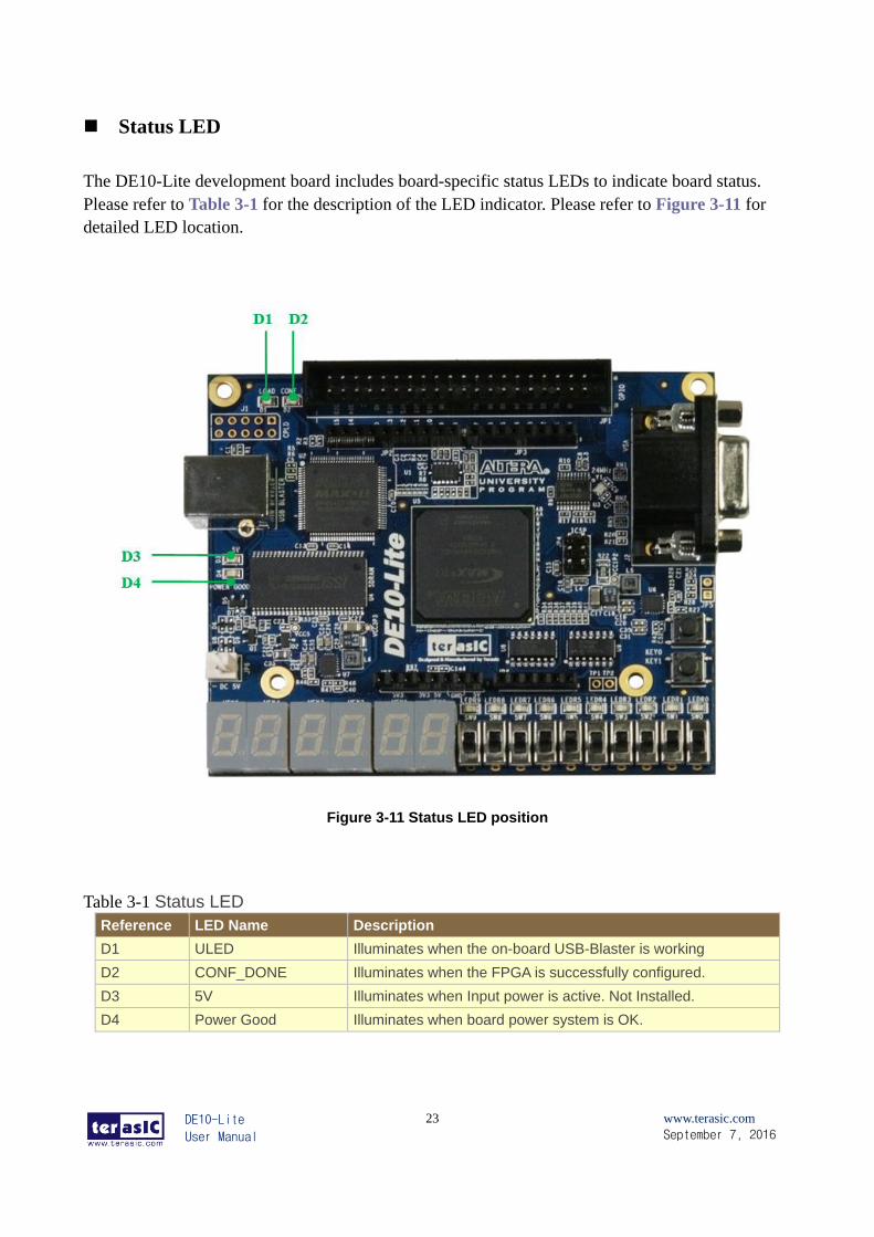
Status LED
The DE10-Lite development board includes board-specific status LEDs to indicate board status.
Please refer to Table 3-1 for the description of the LED indicator. Please refer to Figure 3-11 for
detailed LED location.
Figure 3-11 Status LED position
Table 3-1 Status LED
Reference LED Name Description
D1 ULED Illuminates when the on-board USB-Blaster is working
D2 CONF_DONE Illuminates when the FPGA is successfully configured.
D3 5V Illuminates when Input power is active. Not Installed.
D4 Power Good Illuminates when board power system is OK.
DE10-Lite
User Manual
24
www.terasic.com
September 7, 2016
33.. 22 CClloocckk CCiirrccuuiittrryy
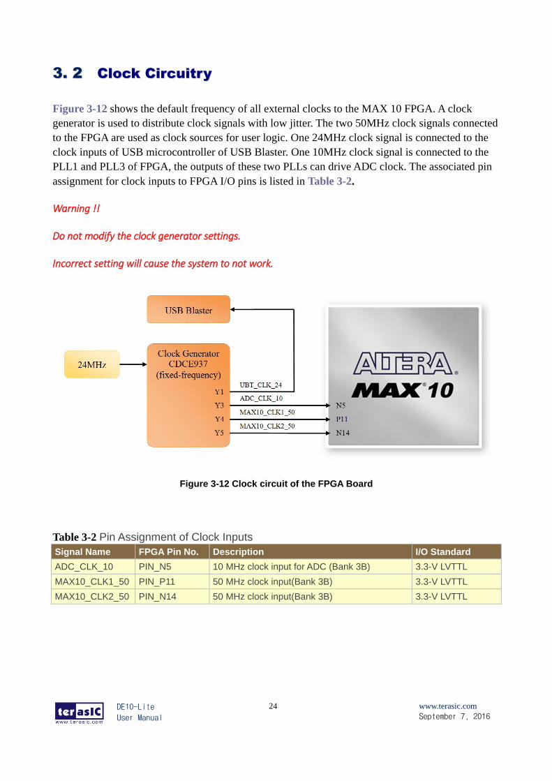
Figure 3-12 shows the default frequency of all external clocks to the MAX 10 FPGA. A clock
generator is used to distribute clock signals with low jitter. The two 50MHz clock signals connected
to the FPGA are used as clock sources for user logic. One 24MHz clock signal is connected to the
clock inputs of USB microcontroller of USB Blaster. One 10MHz clock signal is connected to the
PLL1 and PLL3 of FPGA, the outputs of these two PLLs can drive ADC clock. The associated pin
assignment for clock inputs to FPGA I/O pins is listed in Table 3-2.
Warning !!
Do not modify the clock generator settings.
Incorrect setting will cause the system to not work.
Figure 3-12 Clock circuit of the FPGA Board
Table 3-2 Pin Assignment of Clock Inputs
Signal Name FPGA Pin No. Description I/O Standard
ADC_CLK_10 PIN_N5 10 MHz clock input for ADC (Bank 3B) 3.3-V LVTTL
MAX10_CLK1_50 PIN_P11 50 MHz clock input(Bank 3B) 3.3-V LVTTL
MAX10_CLK2_50 PIN_N14 50 MHz clock input(Bank 3B) 3.3-V LVTTL
DE10-Lite
User Manual
25
www.terasic.com
September 7, 2016
33.. 33 UUssiinngg tthhee PPuusshh--bbuuttttoonnss,, SSwwiittcchheess aanndd LLEEDDss
User-Defined Push-buttons
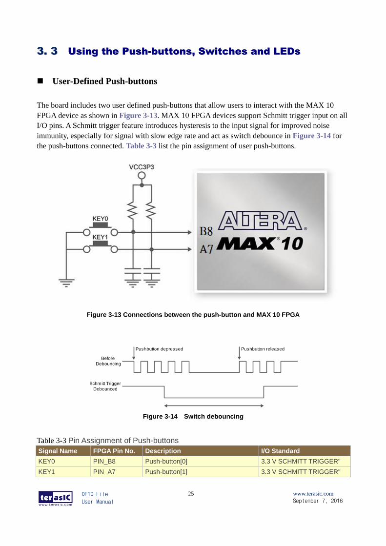
The board includes two user defined push-buttons that allow users to interact with the MAX 10
FPGA device as shown in Figure 3-13. MAX 10 FPGA devices support Schmitt trigger input on all
I/O pins. A Schmitt trigger feature introduces hysteresis to the input signal for improved noise
immunity, especially for signal with slow edge rate and act as switch debounce in Figure 3-14 for
the push-buttons connected. Table 3-3 list the pin assignment of user push-buttons.
Figure 3-13 Connections between the push-button and MAX 10 FPGA
Figure 3-14 Switch debouncing
Table 3-3 Pin Assignment of Push-buttons
Signal Name FPGA Pin No. Description I/O Standard
KEY0 PIN_B8 Push-button[0] 3.3 V SCHMITT TRIGGER"
KEY1 PIN_A7 Push-button[1] 3.3 V SCHMITT TRIGGER"
Pushbutton releasedPushbutton depressed
Before
Debouncing
Schmitt Trigger
Debounced
DE10-Lite
User Manual
26
www.terasic.com
September 7, 2016
User-Defined Slide Switch
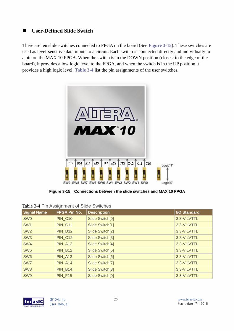
There are ten slide switches connected to FPGA on the board (See Figure 3-15). These switches are
used as level-sensitive data inputs to a circuit. Each switch is connected directly and individually to
a pin on the MAX 10 FPGA. When the switch is in the DOWN position (closest to the edge of the
board), it provides a low logic level to the FPGA, and when the switch is in the UP position it
provides a high logic level. Table 3-4 list the pin assignments of the user switches.
Figure 3-15 Connections between the slide switches and MAX 10 FPGA
Table 3-4 Pin Assignment of Slide Switches
Signal Name FPGA Pin No. Description I/O Standard
SW0 PIN_C10 Slide Switch[0] 3.3-V LVTTL
SW1 PIN_C11 Slide Switch[1] 3.3-V LVTTL
SW2 PIN_D12 Slide Switch[2] 3.3-V LVTTL
SW3 PIN_C12 Slide Switch[3] 3.3-V LVTTL
SW4 PIN_A12 Slide Switch[4] 3.3-V LVTTL
SW5 PIN_B12 Slide Switch[5] 3.3-V LVTTL
SW6 PIN_A13 Slide Switch[6] 3.3-V LVTTL
SW7 PIN_A14 Slide Switch[7] 3.3-V LVTTL
SW8 PIN_B14 Slide Switch[8] 3.3-V LVTTL
SW9 PIN_F15 Slide Switch[9] 3.3-V LVTTL
DE10-Lite
User Manual
27
www.terasic.com
September 7, 2016
User-Defined LEDs
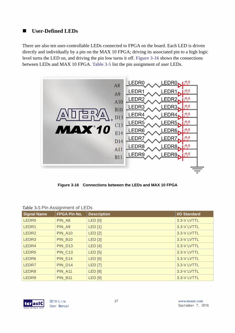
There are also ten user-controllable LEDs connected to FPGA on the board. Each LED is driven
directly and individually by a pin on the MAX 10 FPGA; driving its associated pin to a high logic
level turns the LED on, and driving the pin low turns it off. Figure 3-16 shows the connections
between LEDs and MAX 10 FPGA. Table 3-5 list the pin assignment of user LEDs.
Figure 3-16 Connections between the LEDs and MAX 10 FPGA
Table 3-5 Pin Assignment of LEDs
Signal Name FPGA Pin No. Description I/O Standard
LEDR0 PIN_A8 LED [0] 3.3-V LVTTL
LEDR1 PIN_A9 LED [1] 3.3-V LVTTL
LEDR2 PIN_A10 LED [2] 3.3-V LVTTL
LEDR3 PIN_B10 LED [3] 3.3-V LVTTL
LEDR4 PIN_D13 LED [4] 3.3-V LVTTL
LEDR5 PIN_C13 LED [5] 3.3-V LVTTL
LEDR6 PIN_E14 LED [6] 3.3-V LVTTL
LEDR7 PIN_D14 LED [7] 3.3-V LVTTL
LEDR8 PIN_A11 LED [8] 3.3-V LVTTL
LEDR9 PIN_B11 LED [9] 3.3-V LVTTL
DE10-Lite
User Manual
28
www.terasic.com
September 7, 2016
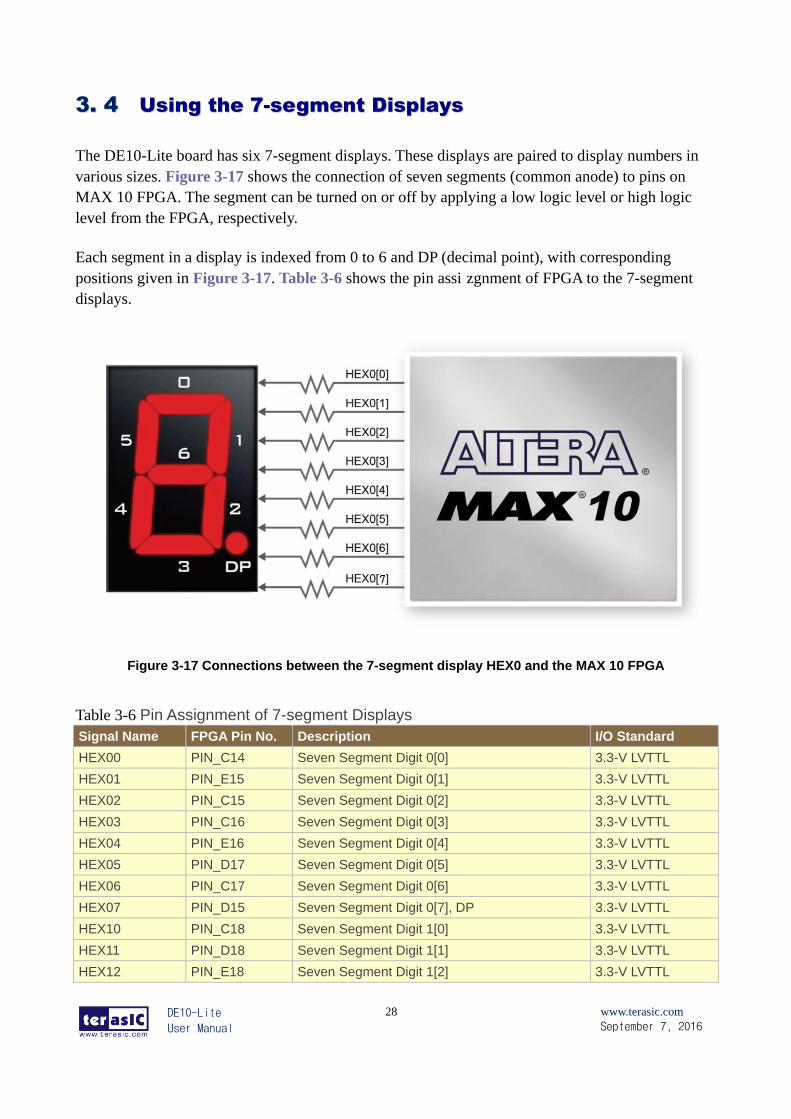
33.. 44 UUssiinngg tthhee 77--sseeggmmeenntt DDiissppllaayyss
The DE10-Lite board has six 7-segment displays. These displays are paired to display numbers in
various sizes. Figure 3-17 shows the connection of seven segments (common anode) to pins on
MAX 10 FPGA. The segment can be turned on or off by applying a low logic level or high logic
level from the FPGA, respectively.
Each segment in a display is indexed from 0 to 6 and DP (decimal point), with corresponding
positions given in Figure 3-17. Table 3-6 shows the pin assi zgnment of FPGA to the 7-segment
displays.
Figure 3-17 Connections between the 7-segment display HEX0 and the MAX 10 FPGA
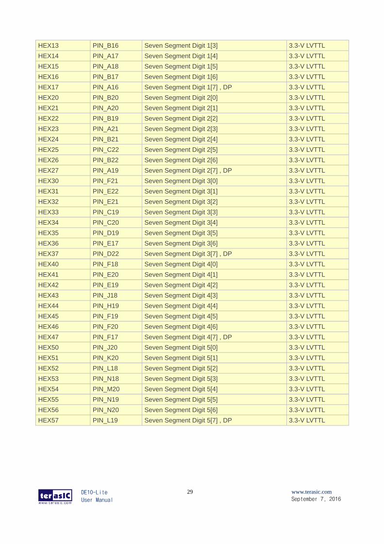
Table 3-6 Pin Assignment of 7-segment Displays
Signal Name FPGA Pin No. Description I/O Standard
HEX00 PIN_C14 Seven Segment Digit 0[0] 3.3-V LVTTL
HEX01 PIN_E15 Seven Segment Digit 0[1] 3.3-V LVTTL
HEX02 PIN_C15 Seven Segment Digit 0[2] 3.3-V LVTTL
HEX03 PIN_C16 Seven Segment Digit 0[3] 3.3-V LVTTL
HEX04 PIN_E16 Seven Segment Digit 0[4] 3.3-V LVTTL
HEX05 PIN_D17 Seven Segment Digit 0[5] 3.3-V LVTTL
HEX06 PIN_C17 Seven Segment Digit 0[6] 3.3-V LVTTL
HEX07 PIN_D15 Seven Segment Digit 0[7], DP 3.3-V LVTTL
HEX10 PIN_C18 Seven Segment Digit 1[0] 3.3-V LVTTL
HEX11 PIN_D18 Seven Segment Digit 1[1] 3.3-V LVTTL
HEX12 PIN_E18 Seven Segment Digit 1[2] 3.3-V LVTTL
DE10-Lite
User Manual
29
www.terasic.com
September 7, 2016
HEX13 PIN_B16 Seven Segment Digit 1[3] 3.3-V LVTTL
HEX14 PIN_A17 Seven Segment Digit 1[4] 3.3-V LVTTL
HEX15 PIN_A18 Seven Segment Digit 1[5] 3.3-V LVTTL
HEX16 PIN_B17 Seven Segment Digit 1[6] 3.3-V LVTTL
HEX17 PIN_A16 Seven Segment Digit 1[7] , DP 3.3-V LVTTL
HEX20 PIN_B20 Seven Segment Digit 2[0] 3.3-V LVTTL
HEX21 PIN_A20 Seven Segment Digit 2[1] 3.3-V LVTTL
HEX22 PIN_B19 Seven Segment Digit 2[2] 3.3-V LVTTL
HEX23 PIN_A21 Seven Segment Digit 2[3] 3.3-V LVTTL
HEX24 PIN_B21 Seven Segment Digit 2[4] 3.3-V LVTTL
HEX25 PIN_C22 Seven Segment Digit 2[5] 3.3-V LVTTL
HEX26 PIN_B22 Seven Segment Digit 2[6] 3.3-V LVTTL
HEX27 PIN_A19 Seven Segment Digit 2[7] , DP 3.3-V LVTTL
HEX30 PIN_F21 Seven Segment Digit 3[0] 3.3-V LVTTL
HEX31 PIN_E22 Seven Segment Digit 3[1] 3.3-V LVTTL
HEX32 PIN_E21 Seven Segment Digit 3[2] 3.3-V LVTTL
HEX33 PIN_C19 Seven Segment Digit 3[3] 3.3-V LVTTL
HEX34 PIN_C20 Seven Segment Digit 3[4] 3.3-V LVTTL
HEX35 PIN_D19 Seven Segment Digit 3[5] 3.3-V LVTTL
HEX36 PIN_E17 Seven Segment Digit 3[6] 3.3-V LVTTL
HEX37 PIN_D22 Seven Segment Digit 3[7] , DP 3.3-V LVTTL
HEX40 PIN_F18 Seven Segment Digit 4[0] 3.3-V LVTTL
HEX41 PIN_E20 Seven Segment Digit 4[1] 3.3-V LVTTL
HEX42 PIN_E19 Seven Segment Digit 4[2] 3.3-V LVTTL
HEX43 PIN_J18 Seven Segment Digit 4[3] 3.3-V LVTTL
HEX44 PIN_H19 Seven Segment Digit 4[4] 3.3-V LVTTL
HEX45 PIN_F19 Seven Segment Digit 4[5] 3.3-V LVTTL
HEX46 PIN_F20 Seven Segment Digit 4[6] 3.3-V LVTTL
HEX47 PIN_F17 Seven Segment Digit 4[7] , DP 3.3-V LVTTL
HEX50 PIN_J20 Seven Segment Digit 5[0] 3.3-V LVTTL
HEX51 PIN_K20 Seven Segment Digit 5[1] 3.3-V LVTTL
HEX52 PIN_L18 Seven Segment Digit 5[2] 3.3-V LVTTL
HEX53 PIN_N18 Seven Segment Digit 5[3] 3.3-V LVTTL
HEX54 PIN_M20 Seven Segment Digit 5[4] 3.3-V LVTTL
HEX55 PIN_N19 Seven Segment Digit 5[5] 3.3-V LVTTL
HEX56 PIN_N20 Seven Segment Digit 5[6] 3.3-V LVTTL
HEX57 PIN_L19 Seven Segment Digit 5[7] , DP 3.3-V LVTTL
DE10-Lite
User Manual
30
www.terasic.com
September 7, 2016
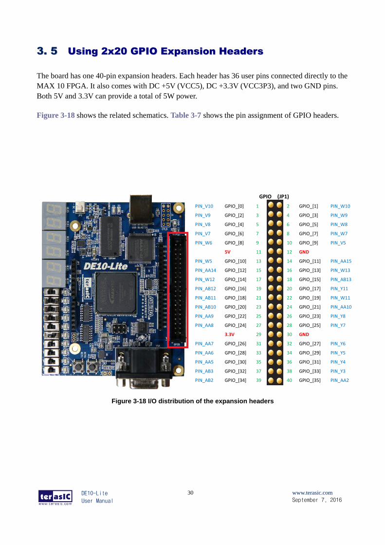
33.. 55 UUssiinngg 22xx2200 GGPPIIOO EExxppaannssiioonn HHeeaaddeerrss
The board has one 40-pin expansion headers. Each header has 36 user pins connected directly to the
MAX 10 FPGA. It also comes with DC +5V (VCC5), DC +3.3V (VCC3P3), and two GND pins.
Both 5V and 3.3V can provide a total of 5W power.
Figure 3-18 shows the related schematics. Table 3-7 shows the pin assignment of GPIO headers.
Figure 3-18 I/O distribution of the expansion headers
GPIO (JP1)
PIN_V10 GPIO_[0] 1 2 GPIO_[1] PIN_W10
PIN_V9 GPIO_[2] 3 4 GPIO_[3] PIN_W9
PIN_V8 GPIO_[4] 5 6 GPIO_[5] PIN_W8
PIN_V7 GPIO_[6] 7 8 GPIO_[7] PIN_W7
PIN_W6 GPIO_[8] 9 10 GPIO_[9] PIN_V5
5V 11 12 GND
PIN_W5 GPIO_[10] 13 14 GPIO_[11] PIN_AA15
PIN_AA14 GPIO_[12] 15 16 GPIO_[13] PIN_W13
PIN_W12 GPIO_[14] 17 18 GPIO_[15] PIN_AB13
PIN_AB12 GPIO_[16] 19 20 GPIO_[17] PIN_Y11
PIN_AB11 GPIO_[18] 21 22 GPIO_[19] PIN_W11
PIN_AB10 GPIO_[20] 23 24 GPIO_[21] PIN_AA10
PIN_AA9 GPIO_[22] 25 26 GPIO_[23] PIN_Y8
PIN_AA8 GPIO_[24] 27 28 GPIO_[25] PIN_Y7
3.3V 29 30 GND
PIN_AA7 GPIO_[26] 31 32 GPIO_[27] PIN_Y6
PIN_AA6 GPIO_[28] 33 34 GPIO_[29] PIN_Y5
PIN_AA5 GPIO_[30] 35 36 GPIO_[31] PIN_Y4
PIN_AB3 GPIO_[32] 37 38 GPIO_[33] PIN_Y3
PIN_AB2 GPIO_[34] 39 40 GPIO_[35] PIN_AA2
DE10-Lite
User Manual
31
www.terasic.com
September 7, 2016
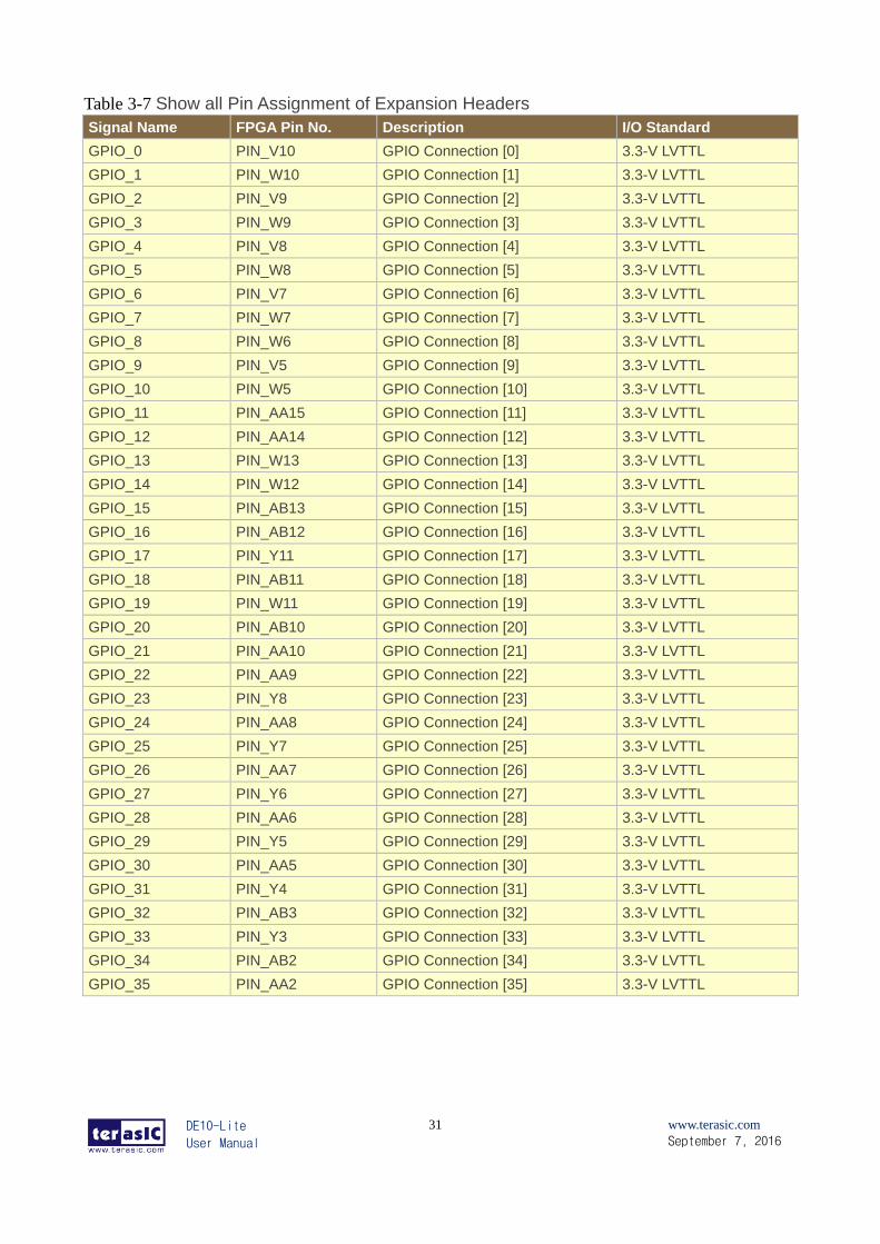
Table 3-7 Show all Pin Assignment of Expansion Headers
Signal Name FPGA Pin No. Description I/O Standard
GPIO_0 PIN_V10 GPIO Connection [0] 3.3-V LVTTL
GPIO_1 PIN_W10 GPIO Connection [1] 3.3-V LVTTL
GPIO_2 PIN_V9 GPIO Connection [2] 3.3-V LVTTL
GPIO_3 PIN_W9 GPIO Connection [3] 3.3-V LVTTL
GPIO_4 PIN_V8 GPIO Connection [4] 3.3-V LVTTL
GPIO_5 PIN_W8 GPIO Connection [5] 3.3-V LVTTL
GPIO_6 PIN_V7 GPIO Connection [6] 3.3-V LVTTL
GPIO_7 PIN_W7 GPIO Connection [7] 3.3-V LVTTL
GPIO_8 PIN_W6 GPIO Connection [8] 3.3-V LVTTL
GPIO_9 PIN_V5 GPIO Connection [9] 3.3-V LVTTL
GPIO_10 PIN_W5 GPIO Connection [10] 3.3-V LVTTL
GPIO_11 PIN_AA15 GPIO Connection [11] 3.3-V LVTTL
GPIO_12 PIN_AA14 GPIO Connection [12] 3.3-V LVTTL
GPIO_13 PIN_W13 GPIO Connection [13] 3.3-V LVTTL
GPIO_14 PIN_W12 GPIO Connection [14] 3.3-V LVTTL
GPIO_15 PIN_AB13 GPIO Connection [15] 3.3-V LVTTL
GPIO_16 PIN_AB12 GPIO Connection [16] 3.3-V LVTTL
GPIO_17 PIN_Y11 GPIO Connection [17] 3.3-V LVTTL
GPIO_18 PIN_AB11 GPIO Connection [18] 3.3-V LVTTL
GPIO_19 PIN_W11 GPIO Connection [19] 3.3-V LVTTL
GPIO_20 PIN_AB10 GPIO Connection [20] 3.3-V LVTTL
GPIO_21 PIN_AA10 GPIO Connection [21] 3.3-V LVTTL
GPIO_22 PIN_AA9 GPIO Connection [22] 3.3-V LVTTL
GPIO_23 PIN_Y8 GPIO Connection [23] 3.3-V LVTTL
GPIO_24 PIN_AA8 GPIO Connection [24] 3.3-V LVTTL
GPIO_25 PIN_Y7 GPIO Connection [25] 3.3-V LVTTL
GPIO_26 PIN_AA7 GPIO Connection [26] 3.3-V LVTTL
GPIO_27 PIN_Y6 GPIO Connection [27] 3.3-V LVTTL
GPIO_28 PIN_AA6 GPIO Connection [28] 3.3-V LVTTL
GPIO_29 PIN_Y5 GPIO Connection [29] 3.3-V LVTTL
GPIO_30 PIN_AA5 GPIO Connection [30] 3.3-V LVTTL
GPIO_31 PIN_Y4 GPIO Connection [31] 3.3-V LVTTL
GPIO_32 PIN_AB3 GPIO Connection [32] 3.3-V LVTTL
GPIO_33 PIN_Y3 GPIO Connection [33] 3.3-V LVTTL
GPIO_34 PIN_AB2 GPIO Connection [34] 3.3-V LVTTL
GPIO_35 PIN_AA2 GPIO Connection [35] 3.3-V LVTTL
DE10-Lite
User Manual
32
www.terasic.com
September 7, 2016
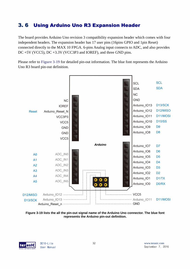
33.. 66 UUssiinngg AArrdduuiinnoo UUnnoo RR33 EExxppaannssiioonn HHeeaaddeerr
The board provides Arduino Uno revision 3 compatibility expansion header which comes with four
independent headers. The expansion header has 17 user pins (16pins GPIO and 1pin Reset)
connected directly to the MAX 10 FPGA. 6-pins Analog input connects to ADC, and also provides
DC +5V (VCC5), DC +3.3V (VCC3P3 and IOREF), and three GND pins.
Please refer to Figure 3-19 for detailed pin-out information. The blue font represents the Arduino
Uno R3 board pin-out definition.
Figure 3-19 lists the all the pin-out signal name of the Arduino Uno connector. The blue font represents the Arduino pin-out definition.
DE10-Lite
User Manual
33
www.terasic.com
September 7, 2016
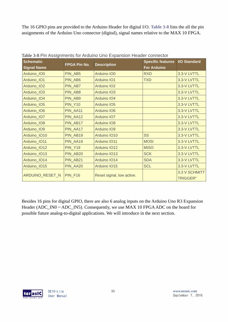
The 16 GPIO pins are provided to the Arduino Header for digital I/O. Table 3-8 lists the all the pin
assignments of the Arduino Uno connector (digital), signal names relative to the MAX 10 FPGA.
Table 3-8 Pin Assignments for Arduino Uno Expansion Header connector
Schematic
Signal Name FPGA Pin No. Description
Specific features
For Arduino
I/O Standard
Arduino_IO0 PIN_AB5 Arduino IO0 RXD 3.3-V LVTTL
Arduino_IO1 PIN_AB6 Arduino IO1 TXD 3.3-V LVTTL
Arduino_IO2 PIN_AB7 Arduino IO2 3.3-V LVTTL
Arduino_IO3 PIN_AB8 Arduino IO3 3.3-V LVTTL
Arduino_IO4 PIN_AB9 Arduino IO4 3.3-V LVTTL
Arduino_IO5 PIN_Y10 Arduino IO5 3.3-V LVTTL
Arduino_IO6 PIN_AA11 Arduino IO6 3.3-V LVTTL
Arduino_IO7 PIN_AA12 Arduino IO7 3.3-V LVTTL
Arduino_IO8 PIN_AB17 Arduino IO8 3.3-V LVTTL
Arduino_IO9 PIN_AA17 Arduino IO9 3.3-V LVTTL
Arduino_IO10 PIN_AB19 Arduino IO10 SS 3.3-V LVTTL
Arduino_IO11 PIN_AA19 Arduino IO11 MOSI 3.3-V LVTTL
Arduino_IO12 PIN_Y19 Arduino IO12 MISO 3.3-V LVTTL
Arduino_IO13 PIN_AB20 Arduino IO13 SCK 3.3-V LVTTL
Arduino_IO14 PIN_AB21 Arduino IO14 SDA 3.3-V LVTTL
Arduino_IO15 PIN_AA20 Arduino IO15 SCL 3.3-V LVTTL
ARDUINO_RESET_N PIN_F16 Reset signal, low active. 3.3 V SCHMITT
TRIGGER"
Besides 16 pins for digital GPIO, there are also 6 analog inputs on the Arduino Uno R3 Expansion
Header (ADC_IN0 ~ ADC_IN5). Consequently, we use MAX 10 FPGA ADC on the board for
possible future analog-to-digital applications. We will introduce in the next section.
DE10-Lite
User Manual
34
www.terasic.com
September 7, 2016
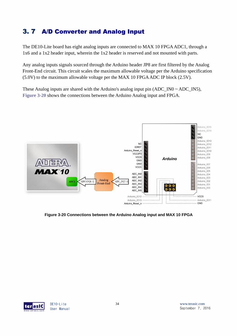
33.. 77 AA//DD CCoonnvveerrtteerr aanndd AAnnaalloogg IInnppuutt
The DE10-Lite board has eight analog inputs are connected to MAX 10 FPGA ADC1, through a
1x6 and a 1x2 header input, wherein the 1x2 header is reserved and not mounted with parts.
Any analog inputs signals sourced through the Arduino header JP8 are first filtered by the Analog
Front-End circuit. This circuit scales the maximum allowable voltage per the Arduino specification
(5.0V) to the maximum allowable voltage per the MAX 10 FPGA ADC IP block (2.5V).
These Analog inputs are shared with the Arduino's analog input pin (ADC_IN0 ~ ADC_IN5),
Figure 3-20 shows the connections between the Arduino Analog input and FPGA.
Figure 3-20 Connections between the Arduino Analog input and MAX 10 FPGA
DE10-Lite
User Manual
35
www.terasic.com
September 7, 2016
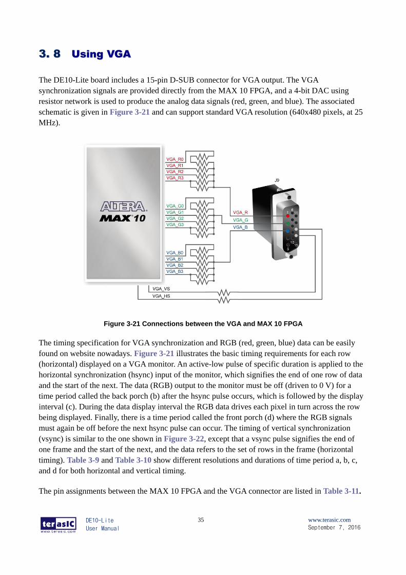
33.. 88 UUssiinngg VVGGAA
The DE10-Lite board includes a 15-pin D-SUB connector for VGA output. The VGA
synchronization signals are provided directly from the MAX 10 FPGA, and a 4-bit DAC using
resistor network is used to produce the analog data signals (red, green, and blue). The associated
schematic is given in Figure 3-21 and can support standard VGA resolution (640x480 pixels, at 25
MHz).
Figure 3-21 Connections between the VGA and MAX 10 FPGA
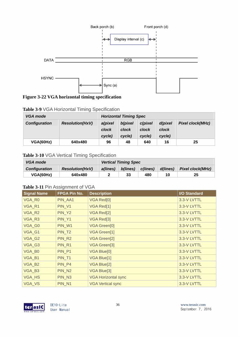
The timing specification for VGA synchronization and RGB (red, green, blue) data can be easily
found on website nowadays. Figure 3-21 illustrates the basic timing requirements for each row
(horizontal) displayed on a VGA monitor. An active-low pulse of specific duration is applied to the
horizontal synchronization (hsync) input of the monitor, which signifies the end of one row of data
and the start of the next. The data (RGB) output to the monitor must be off (driven to 0 V) for a
time period called the back porch (b) after the hsync pulse occurs, which is followed by the display
interval (c). During the data display interval the RGB data drives each pixel in turn across the row
being displayed. Finally, there is a time period called the front porch (d) where the RGB signals
must again be off before the next hsync pulse can occur. The timing of vertical synchronization
(vsync) is similar to the one shown in Figure 3-22, except that a vsync pulse signifies the end of
one frame and the start of the next, and the data refers to the set of rows in the frame (horizontal
timing). Table 3-9 and Table 3-10 show different resolutions and durations of time period a, b, c,
and d for both horizontal and vertical timing.
The pin assignments between the MAX 10 FPGA and the VGA connector are listed in Table 3-11.
DE10-Lite
User Manual
36
www.terasic.com
September 7, 2016
Figure 3-22 VGA horizontal timing specification
Table 3-9 VGA Horizontal Timing Specification
VGA mode Horizontal Timing Spec
Configuration Resolution(HxV) a(pixel
clock
cycle)
b(pixel
clock
cycle)
c(pixel
clock
cycle)
d(pixel
clock
cycle)
Pixel clock(MHz)
VGA(60Hz) 640x480 96 48 640 16 25
Table 3-10 VGA Vertical Timing Specification
VGA mode Vertical Timing Spec
Configuration Resolution(HxV) a(lines) b(lines) c(lines) d(lines) Pixel clock(MHz)
VGA(60Hz) 640x480 2 33 480 10 25
Table 3-11 Pin Assignment of VGA
Signal Name FPGA Pin No. Description I/O Standard
VGA_R0 PIN_AA1 VGA Red[0] 3.3-V LVTTL
VGA_R1 PIN_V1 VGA Red[1] 3.3-V LVTTL
VGA_R2 PIN_Y2 VGA Red[2] 3.3-V LVTTL
VGA_R3 PIN_Y1 VGA Red[3] 3.3-V LVTTL
VGA_G0 PIN_W1 VGA Green[0] 3.3-V LVTTL
VGA_G1 PIN_T2 VGA Green[1] 3.3-V LVTTL
VGA_G2 PIN_R2 VGA Green[2] 3.3-V LVTTL
VGA_G3 PIN_R1 VGA Green[3] 3.3-V LVTTL
VGA_B0 PIN_P1 VGA Blue[0] 3.3-V LVTTL
VGA_B1 PIN_T1 VGA Blue[1] 3.3-V LVTTL
VGA_B2 PIN_P4 VGA Blue[2] 3.3-V LVTTL
VGA_B3 PIN_N2 VGA Blue[3] 3.3-V LVTTL
VGA_HS PIN_N3 VGA Horizontal sync 3.3-V LVTTL
VGA_VS PIN_N1 VGA Vertical sync 3.3-V LVTTL
DE10-Lite
User Manual
37
www.terasic.com
September 7, 2016
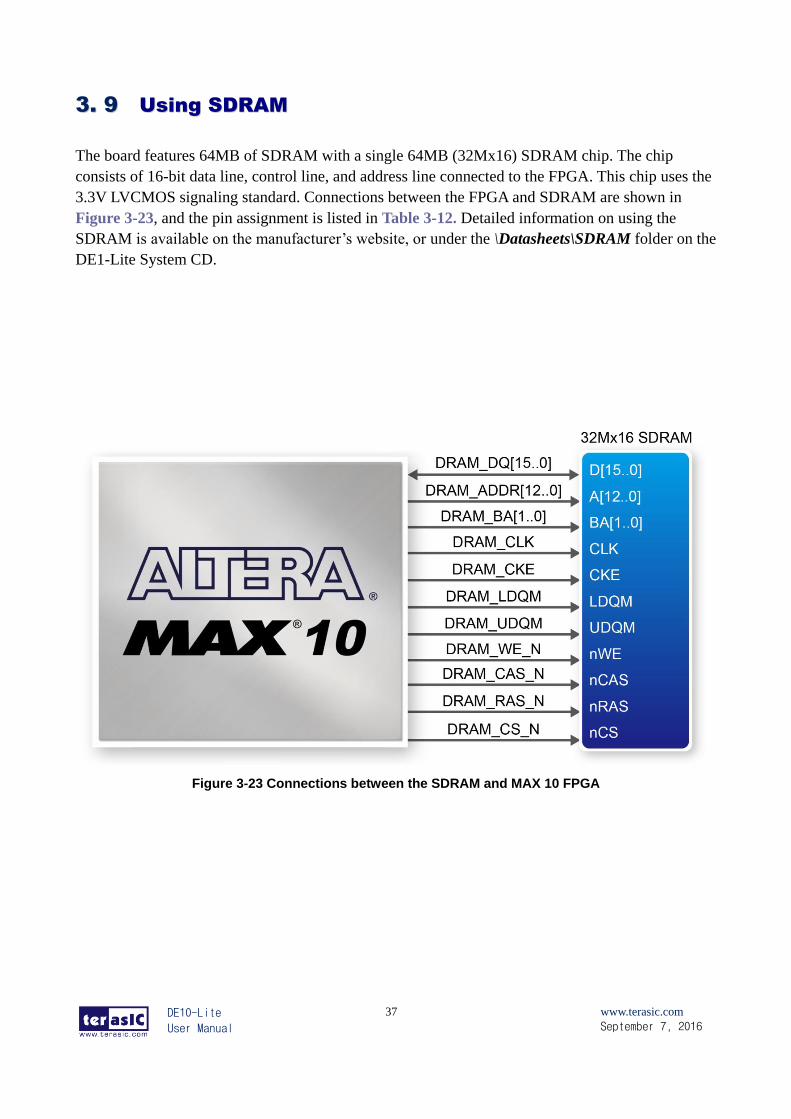
33.. 99 UUssiinngg SSDDRRAAMM
The board features 64MB of SDRAM with a single 64MB (32Mx16) SDRAM chip. The chip
consists of 16-bit data line, control line, and address line connected to the FPGA. This chip uses the
3.3V LVCMOS signaling standard. Connections between the FPGA and SDRAM are shown in
Figure 3-23, and the pin assignment is listed in Table 3-12. Detailed information on using the
SDRAM is available on the manufacturer’s website, or under the \Datasheets\SDRAM folder on the
DE1-Lite System CD.
Figure 3-23 Connections between the SDRAM and MAX 10 FPGA

DE10-Lite
User Manual
38
www.terasic.com
September 7, 2016
Table 3-12 Pin Assignment of SDRAM
Signal Name FPGA Pin No. Description I/O Standard
DRAM_ADDR0 PIN_U17 SDRAM Address[0] 3.3-V LVTTL
DRAM_ADDR1 PIN_W19 SDRAM Address[1] 3.3-V LVTTL
DRAM_ADDR2 PIN_V18 SDRAM Address[2] 3.3-V LVTTL
DRAM_ADDR3 PIN_U18 SDRAM Address[3] 3.3-V LVTTL
DRAM_ADDR4 PIN_U19 SDRAM Address[4] 3.3-V LVTTL
DRAM_ADDR5 PIN_T18 SDRAM Address[5] 3.3-V LVTTL
DRAM_ADDR6 PIN_T19 SDRAM Address[6] 3.3-V LVTTL
DRAM_ADDR7 PIN_R18 SDRAM Address[7] 3.3-V LVTTL
DRAM_ADDR8 PIN_P18 SDRAM Address[8] 3.3-V LVTTL
DRAM_ADDR9 PIN_P19 SDRAM Address[9] 3.3-V LVTTL
DRAM_ADDR10 PIN_T20 SDRAM Address[10] 3.3-V LVTTL
DRAM_ADDR11 PIN_P20 SDRAM Address[11] 3.3-V LVTTL
DRAM_ADDR12 PIN_R20 SDRAM Address[12] 3.3-V LVTTL
DRAM_DQ0 PIN_Y21 SDRAM Data[0] 3.3-V LVTTL
DRAM_DQ1 PIN_Y20 SDRAM Data[1] 3.3-V LVTTL
DRAM_DQ2 PIN_AA2 SDRAM Data[2] 3.3-V LVTTL
DRAM_DQ3 PIN_AA2 SDRAM Data[3] 3.3-V LVTTL
DRAM_DQ4 PIN_Y22 SDRAM Data[4] 3.3-V LVTTL
DRAM_DQ5 PIN_W22 SDRAM Data[5] 3.3-V LVTTL
DRAM_DQ6 PIN_W20 SDRAM Data[6] 3.3-V LVTTL
DRAM_DQ7 PIN_V21 SDRAM Data[7] 3.3-V LVTTL
DRAM_DQ8 PIN_P21 SDRAM Data[8] 3.3-V LVTTL
DRAM_DQ9 PIN_J22 SDRAM Data[9] 3.3-V LVTTL
DRAM_DQ10 PIN_H21 SDRAM Data[10] 3.3-V LVTTL
DRAM_DQ11 PIN_H22 SDRAM Data[11] 3.3-V LVTTL
DRAM_DQ12 PIN_G22 SDRAM Data[12] 3.3-V LVTTL
DRAM_DQ13 PIN_G20 SDRAM Data[13] 3.3-V LVTTL
DRAM_DQ14 PIN_G19 SDRAM Data[14] 3.3-V LVTTL
DRAM_DQ15 PIN_F22 SDRAM Data[15] 3.3-V LVTTL
DRAM_BA0 PIN_T21 SDRAM Bank Address[0] 3.3-V LVTTL
DRAM_BA1 PIN_T22 SDRAM Bank Address[1] 3.3-V LVTTL
DRAM_LDQM PIN_V22 SDRAM byte Data Mask[0] 3.3-V LVTTL
DRAM_UDQM PIN_J21 SDRAM byte Data Mask[1] 3.3-V LVTTL
DRAM_RAS_N PIN_U22 SDRAM Row Address Strobe 3.3-V LVTTL
DRAM_CAS_N PIN_U21 SDRAM Column Address Strobe 3.3-V LVTTL
DRAM_CKE PIN_N22 SDRAM Clock Enable 3.3-V LVTTL
DRAM_CLK PIN_L14 SDRAM Clock 3.3-V LVTTL
DRAM_WE_N PIN_V20 SDRAM Write Enable 3.3-V LVTTL
DRAM_CS_N PIN_U20 SDRAM Chip Select 3.3-V LVTTL

DE10-Lite
User Manual
39
www.terasic.com
September 7, 2016
33.. 1100 UUssiinngg AAcccceelleerroommeetteerr SSeennssoorr
The board comes with a digital accelerometer sensor module (ADXL345), commonly known as
G-sensor. This G-sensor is a small, thin, ultralow power assumption 3-axis accelerometer with
high-resolution measurement. Digitalized output is formatted as 16-bit in two’s complement and
can be accessed through SPI (3- and 4-wire) and I2C digital interfaces.
With GSENSOR_CS_N signal to high, the ADXL345 is in I2C mode. With the GSENSOR_SDO
signal to high, the 7-bit I2C address for the device is 0x1D, followed by the R/W bit. This translates
to 0x3A for a write and 0x3B for a read. An alternate I2C address of 0x53 (followed by the R/W bit)
can be chosen by low the GSENSOR_SDO signal. This translates to 0xA6 for a write and 0xA7 for
a read.
More information about this chip can be found in its datasheet, which is available on manufacturer’s
website or in the directory \Datasheet\G-Sensor folder of DE1-Lite system CD.
Figure 3-24 shows the connections between the accelerometer sensor and MAX 10 FPGA. Table
3-13 lists the pin assignment of accelerometer to the MAX 10 FPGA.
Figure 3-24 shows the connections between the accelerometer sensor and MAX 10 FPGA.
DE10-Lite
User Manual
40
www.terasic.com
September 7, 2016
Table 3-13 Pin Assignment of Accelerometer Sensor
Signal Name FPGA Pin No. Description I/O Standard
GSENSOR_SDI PIN_V11
I2C serial data
SPI serial data input (SPI 4-wire)
SPI serial data input and output (SPI 3-wire)
3.3-V LVTTL
GSENSOR_SDO PIN_V12 SPI serial data output (SPI 4-wire)
Alternate I2C address select 3.3-V LVTTL
GSENSOR_CS_n PIN_AB16
I2C/SPI mode selection:
1: SPI idle mode / I2C communication enabled
0: SPI communication mode / I2C disabled
SPI Chip Select
3.3-V LVTTL
GSENSOR_SCLK PIN_AB15 I2C serial clock
SPI serial clock (3- and 4-wire) 3.3-V LVTTL
GSENSOR_INT1 PIN_Y14 Interrupt pin 1 3.3-V LVTTL
GSENSOR_INT2 PIN_Y13 Interrupt pin 2 3.3-V LVTTL
DE10-Lite
User Manual
41
www.terasic.com
September 7, 2016
Chapter 4
DE10-Lite System Builder
This chapter describes how users can create a custom design project with the tool named DE10-Lite
System Builder.
44.. 11 IInnttrroodduuccttiioonn
The DE10-Lite System Builder is a Windows-based utility. It is designed to help users create a
Quartus II project for DE10-Lite within minutes. The generated Quartus II project files include:
Quartus II project file (.qpf)
Quartus II setting file (.qsf)
Top-level design file (.v)
Synopsis design constraints file (.sdc)
Pin assignment document (.htm)
The above files generated by the DE10-Lite System Builder can also prevent occurrence of
situations that are prone to compilation error when users manually edit the top-level design file or
place pin assignment. The common mistakes that users encounter are:
Board is damaged due to incorrect bank voltage setting or pin assignment.
Board is malfunctioned because of wrong device chosen, declaration of pin location or direction
is incorrect or forgotten.
Performance degradation due to improper pin assignment.
DE10-Lite
User Manual
42
www.terasic.com
September 7, 2016
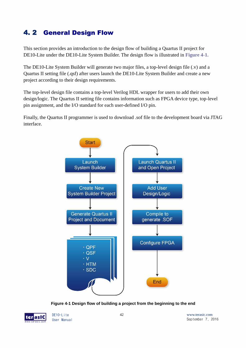
44.. 22 GGeenneerraall DDeessiiggnn FFllooww
This section provides an introduction to the design flow of building a Quartus II project for
DE10-Lite under the DE10-Lite System Builder. The design flow is illustrated in Figure 4-1.
The DE10-Lite System Builder will generate two major files, a top-level design file (.v) and a
Quartus II setting file (.qsf) after users launch the DE10-Lite System Builder and create a new
project according to their design requirements.
The top-level design file contains a top-level Verilog HDL wrapper for users to add their own
design/logic. The Quartus II setting file contains information such as FPGA device type, top-level
pin assignment, and the I/O standard for each user-defined I/O pin.
Finally, the Quartus II programmer is used to download .sof file to the development board via JTAG
interface.
Figure 4-1 Design flow of building a project from the beginning to the end
DE10-Lite
User Manual
43
www.terasic.com
September 7, 2016
44.. 33 UUssiinngg DDEE1100--LLiittee SSyysstteemm BBuuiillddeerr
This section provides the procedures in details on how to use the DE10-Lite System Builder.
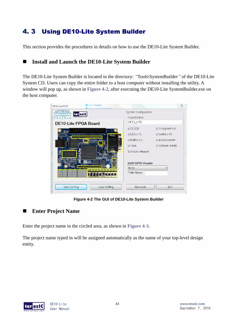
Install and Launch the DE10-Lite System Builder
The DE10-Lite System Builder is located in the directory: “Tools\SystemBuilder” of the DE10-Lite
System CD. Users can copy the entire folder to a host computer without installing the utility. A
window will pop up, as shown in Figure 4-2, after executing the DE10-Lite SystemBuilder.exe on
the host computer.
Figure 4-2 The GUI of DE10-Lite System Builder
Enter Project Name
Enter the project name in the circled area, as shown in Figure 4-3.
The project name typed in will be assigned automatically as the name of your top-level design
entity.
DE10-Lite
User Manual
44
www.terasic.com
September 7, 2016
Figure 4-3 Enter the project name
System Configuration
Users are given the flexibility in the System Configuration to include their choice of components in
the project, as shown in Figure 4-4. Each component onboard is listed and users can enable or
disable one or more components at will. If a component is enabled, the DE10-Lite System Builder
will automatically generate its associated pin assignment, including the pin name, pin location, pin
direction, and I/O standard.
Figure 4-4 System configuration group

DE10-Lite
User Manual
45
www.terasic.com
September 7, 2016
GPIO Expansion
If users connect any Terasic GPIO-based daughter card to the GPIO connector(s) on DE10-Lite, the
DE10-Lite System Builder can generate a project that include the corresponding module, as shown
in Figure 4-5. It will also generate the associated pin assignment automatically, including pin name,
pin location, pin direction, and I/O standard.
Figure 4-5 GPIO expansion group
The “Prefix Name” is an optional feature that denote the pin name of the daughter card assigned in
your design. Users may leave this field blank.
DE10-Lite
User Manual
46
www.terasic.com
September 7, 2016
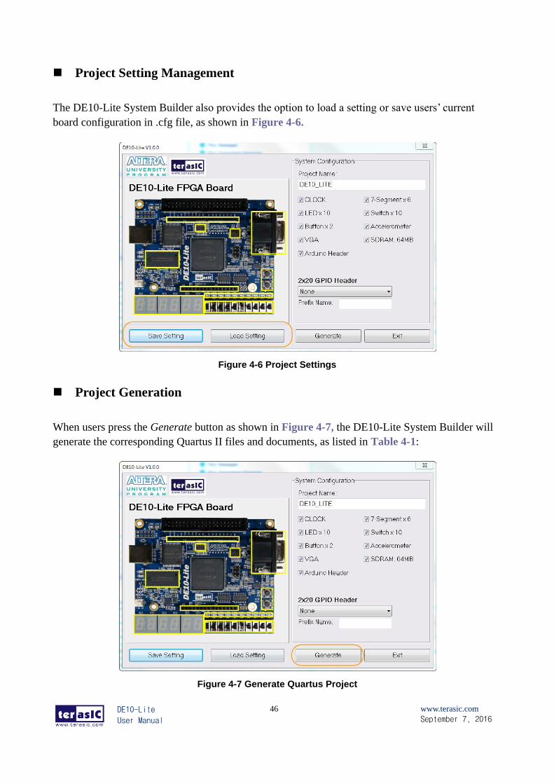
Project Setting Management
The DE10-Lite System Builder also provides the option to load a setting or save users’ current
board configuration in .cfg file, as shown in Figure 4-6.
Figure 4-6 Project Settings
Project Generation
When users press the Generate button as shown in Figure 4-7, the DE10-Lite System Builder will
generate the corresponding Quartus II files and documents, as listed in Table 4-1:
Figure 4-7 Generate Quartus Project
DE10-Lite
User Manual
47
www.terasic.com
September 7, 2016
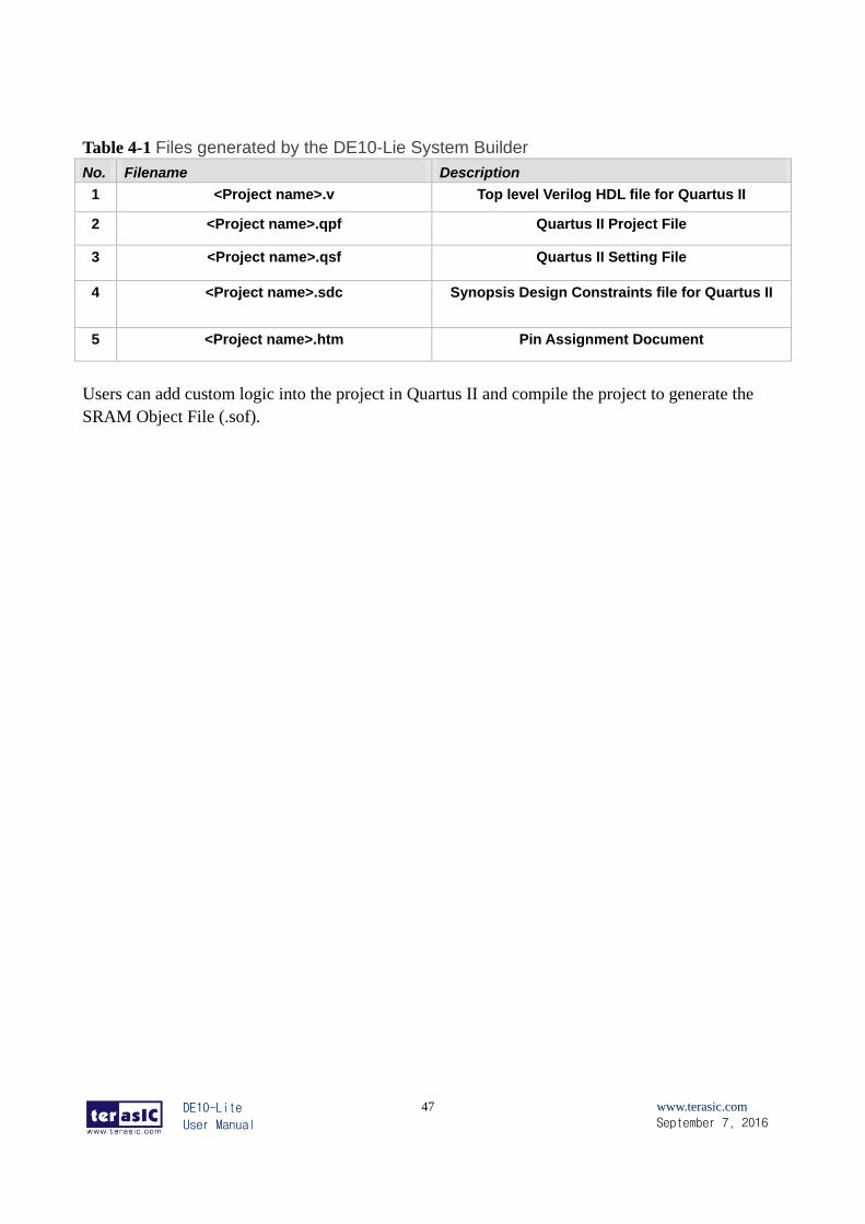
Table 4-1 Files generated by the DE10-Lie System Builder
No. Filename Description
1 <Project name>.v Top level Verilog HDL file for Quartus II
2 <Project name>.qpf Quartus II Project File
3 <Project name>.qsf Quartus II Setting File
4 <Project name>.sdc Synopsis Design Constraints file for Quartus II
5 <Project name>.htm Pin Assignment Document
Users can add custom logic into the project in Quartus II and compile the project to generate the
SRAM Object File (.sof).
DE10-Lite
User Manual
48
www.terasic.com
September 7, 2016
Chapter 5
Examples of Advanced
Demonstrations
This chapter provides examples of advanced designs implemented by RTL or Qsys on the
DE10-Lite board. These reference designs cover the features of peripherals connected to the FPGA,
such as VGA, SDRAM, and SD card. All the associated files can be found in the directory
\Demonstrations of DE10-Lite System CD.
Installation of Demonstrations
To install the demonstrations on your computer:
Copy the folder Demonstrations to a local directory of your choice. It is important to make sure the
path to your local directory contains NO space. Otherwise it will lead to error in Nios II.
Note : Quartus II v16.0 or later is required for all DE10-Lite demonstrations to support MAX 10
FPGA device.
55.. 11 DDEE1100--LLiittee FFaaccttoorryy CCoonnffiigguurraattiioonn
The DE10-Lite board has a default configuration bit-stream pre-programmed, which demonstrates
some of the basic features onboard. The setup required for this demonstration and the location of its
files are shown below.
DDeemmoonnssttrraattiioonn FFiillee LLooccaattiioonnss
Project directory: \Default
Bitstream used: DE10_LITE_Default.sof , DE10_LITE_Default.pof
DE10-Lite
User Manual
49
www.terasic.com
September 7, 2016
DDeemmoonnssttrraattiioonn SSeettuupp aanndd IInnssttrruuccttiioonnss
Connect the DE10-Lite board (J3) to the host PC with a USB cable and install the USB-Blaster
driver if necessary.
Execute the demo batch file “ test.bat” from the directory \Default\demo_batch\
You should now be able to observe the 7-segment displays are showing a sequence of characters,
and the red LEDs are blinking.
Press KEY0 to make LEDs and 7 SEGs all light on.
If the VGA D-SUB connector is connected to a VGA display, it would show a color picture.
RReessttoorree FFaaccttoorryy CCoonnffiigguurraattiioonn
Connect the DE10-Lite board (J3) to the host PC with a USB cable and install the USB-Blaster
driver if necessary.
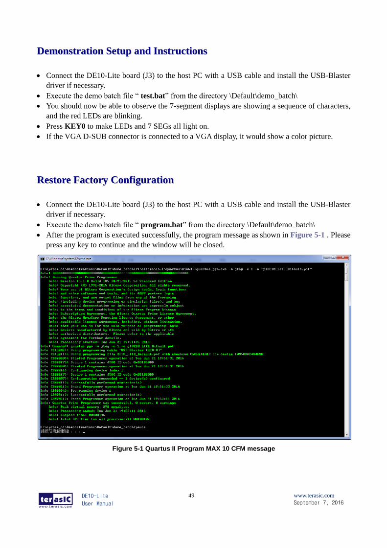
Execute the demo batch file “ program.bat” from the directory \Default\demo_batch\
After the program is executed successfully, the program message as shown in Figure 5-1 . Please
press any key to continue and the window will be closed.
Figure 5-1 Quartus II Program MAX 10 CFM message
DE10-Lite
User Manual
50
www.terasic.com
September 7, 2016
55.. 22 SSDDRRAAMM TTeesstt iinn NNiiooss IIII
There are many applications using SDRAM as a temporary storage. Both hardware and software
designs are provided to illustrate how to perform memory access in Qsys in this demonstration. It
also shows how Altera’s SDRAM controller IP accesses SDRAM and how the Nios II processor
reads and writes the SDRAM for hardware verification. The SDRAM controller handles complex
aspects of accessing SDRAM such as initializing the memory device, managing SDRAM banks,
and keeping the devices refreshed at certain interval.
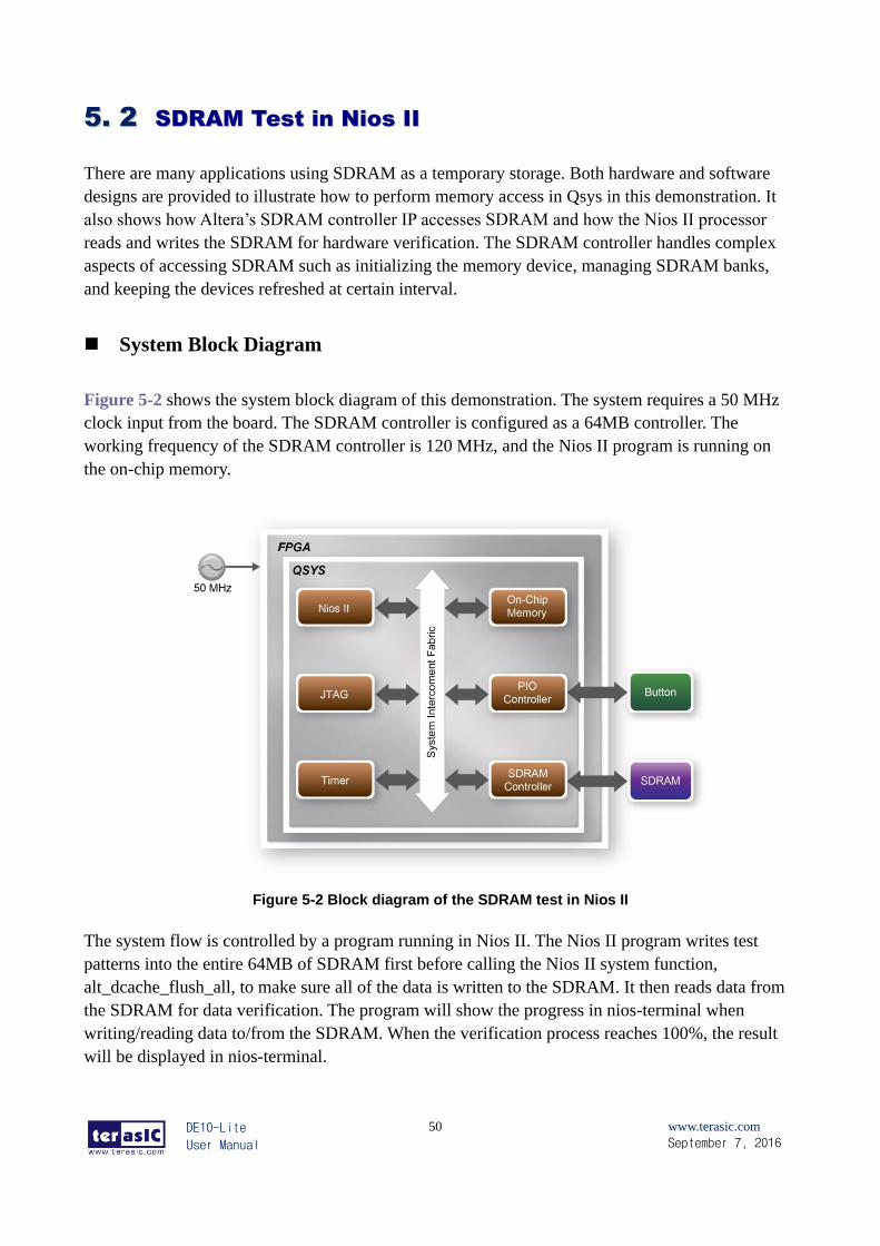
System Block Diagram
Figure 5-2 shows the system block diagram of this demonstration. The system requires a 50 MHz
clock input from the board. The SDRAM controller is configured as a 64MB controller. The
working frequency of the SDRAM controller is 120 MHz, and the Nios II program is running on
the on-chip memory.
Figure 5-2 Block diagram of the SDRAM test in Nios II
The system flow is controlled by a program running in Nios II. The Nios II program writes test
patterns into the entire 64MB of SDRAM first before calling the Nios II system function,
alt_dcache_flush_all, to make sure all of the data is written to the SDRAM. It then reads data from
the SDRAM for data verification. The program will show the progress in nios-terminal when
writing/reading data to/from the SDRAM. When the verification process reaches 100%, the result
will be displayed in nios-terminal.
DE10-Lite
User Manual
51
www.terasic.com
September 7, 2016
DDeessiiggnn TToooollss
Quartus II v16.0
Nios II Eclipse v16.0
DDeemmoonnssttrraattiioonn SSoouurrccee CCooddee
Quartus project directory: \SDRAM_Nios_Test
Nios II Eclipse directory: \SDRAM_Nios_Test \Software
NNiiooss IIII PPrroojjeecctt CCoommppiillaattiioonn
Click “Clean” from the “Project” menu of Nios II Eclipse before compiling the reference design
in Nios II Eclipse.
DDeemmoonnssttrraattiioonn BBaattcchh FFiillee
The files are located in the director: \SDRAM_Nios_Test\demo_batch
The folder includes the following files:
Batch file for USB-Blaster : test.bat and test.sh
FPGA configuration file : DE10_LITE_SDRAM_Nios_Test.sof
Nios II program: DE10_LITE_SDRAM_Nios_Test.elf
DDeemmoonnssttrraattiioonn SSeettuupp
Quartus II v16.0 and Nios II v16.0 must be pre-installed on the host PC.
Connect the DE10-Lite board (J3) to the host PC with a USB cable and install the USB-Blaster
driver if necessary.
Execute the demo batch file “test.bat” from the directory \SDRAM_Nios_Test\demo_batch
After the program is downloaded and executed successfully, a prompt message will be displayed
in nios2-terminal.
Press any button (KEY0~KEY1) to start the SDRAM verification process. Press KEY0 to run
the test continuously.
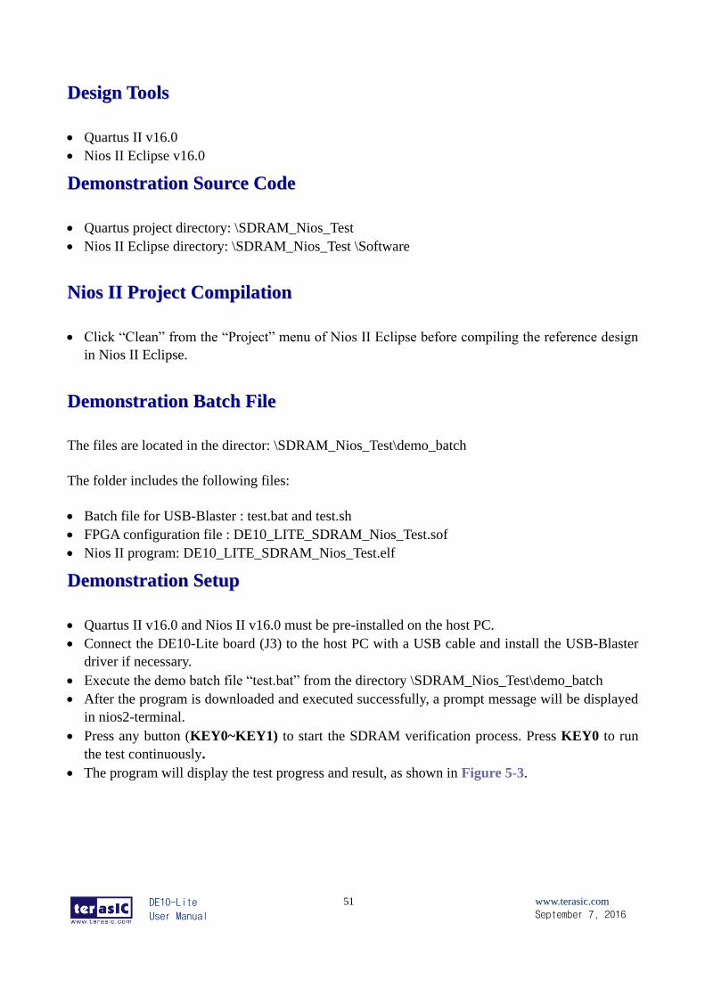
The program will display the test progress and result, as shown in Figure 5-3.
DE10-Lite
User Manual
52
www.terasic.com
September 7, 2016
Figure 5-3 Display of progress and result for the SDRAM test in Nios II
DE10-Lite
User Manual
53
www.terasic.com
September 7, 2016
55.. 33 SSDDRRAAMM TTeesstt iinn VVeerriilloogg
DE10-Lite system CD offers another SDRAM test with its test code written in Verilog HDL. The
memory size of the SDRAM bank tested is still 64MB.
Function Block Diagram
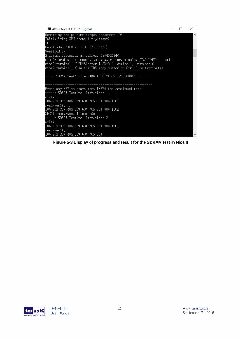
Figure 5-4 shows the function block diagram of this demonstration. The SDRAM controller uses 50
MHz as a reference clock and generates 100 MHz as the memory clock.
Figure 5-4 Block diagram of the SDRAM test in Verilog
RW_Test module writes the entire memory with a test sequence first before comparing the data read
back with the regenerated test sequence, which is the same as the data written to the memory.
KEY0 triggers test control signals for the SDRAM, and the LEDs will indicate the test result
according to Table 5-1.
DDeessiiggnn TToooollss
Quartus II v16.0
DDeemmoonnssttrraattiioonn SSoouurrccee CCooddee
Project directory: \DE10_LITE_SDRAM_RTL_Test
Bit-stream used: DE10_LITE_SDRAM_RTL_Test.sof

DE10-Lite
User Manual
54
www.terasic.com
September 7, 2016
DDeemmoonnssttrraattiioonn BBaattcchh FFiillee
Demo batch file folder: \DE10_LITE_SDRAM_RTL_Test\demo_batch
The directory includes the following files:
Batch file : Test.bat
FPGA configuration file : DE10_LITE_SDRAM_RTL_Test.sof
DDeemmoonnssttrraattiioonn SSeettuupp
Quartus II v16.0 must be pre-installed to the host PC.
Connect the DE10-Lite board (J3) to the host PC with a USB cable and install the USB-Blaster
driver if necessary
Execute the demo batch file “DE10_LITE_SDRAM_RTL_Test.bat” from the directory
\DE10_LITE_SDRAM_RTL_Test\demo_batch
Press KEY0 on the DE10-Lite board to start the verification process. When KEY0 is pressed,
the LEDR [2:0] should turn on. When KEY0 is then released, LEDR1 and LEDR2 should start
blinking.
After approximately 8 seconds, LEDR1 should stop blinking and stay ON to indicate the test is
PASS. Table 5-1 lists the status of LED indicators.
If LEDR2 is not blinking, it means 50MHz clock source is not working.
If LEDR1 failed to remain ON after approximately 8 seconds, the SDRAM test is NG.
Press KEY0 again to repeat the SDRAM test.
Table 5-1 Status of LED Indicators
Name Description
LEDR1 ON if the test is PASS after releasing KEY0
LEDR2 Blinks
DE10-Lite
User Manual
55
www.terasic.com
September 7, 2016
55.. 44 VVGGAA PPaatttteerrnn
This demonstration displays a simple blue, red and green color pattern on a VGA monitor using the
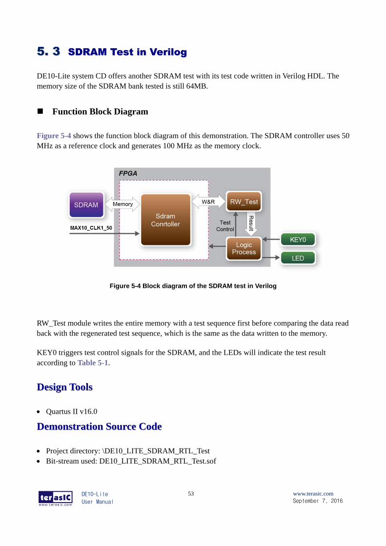
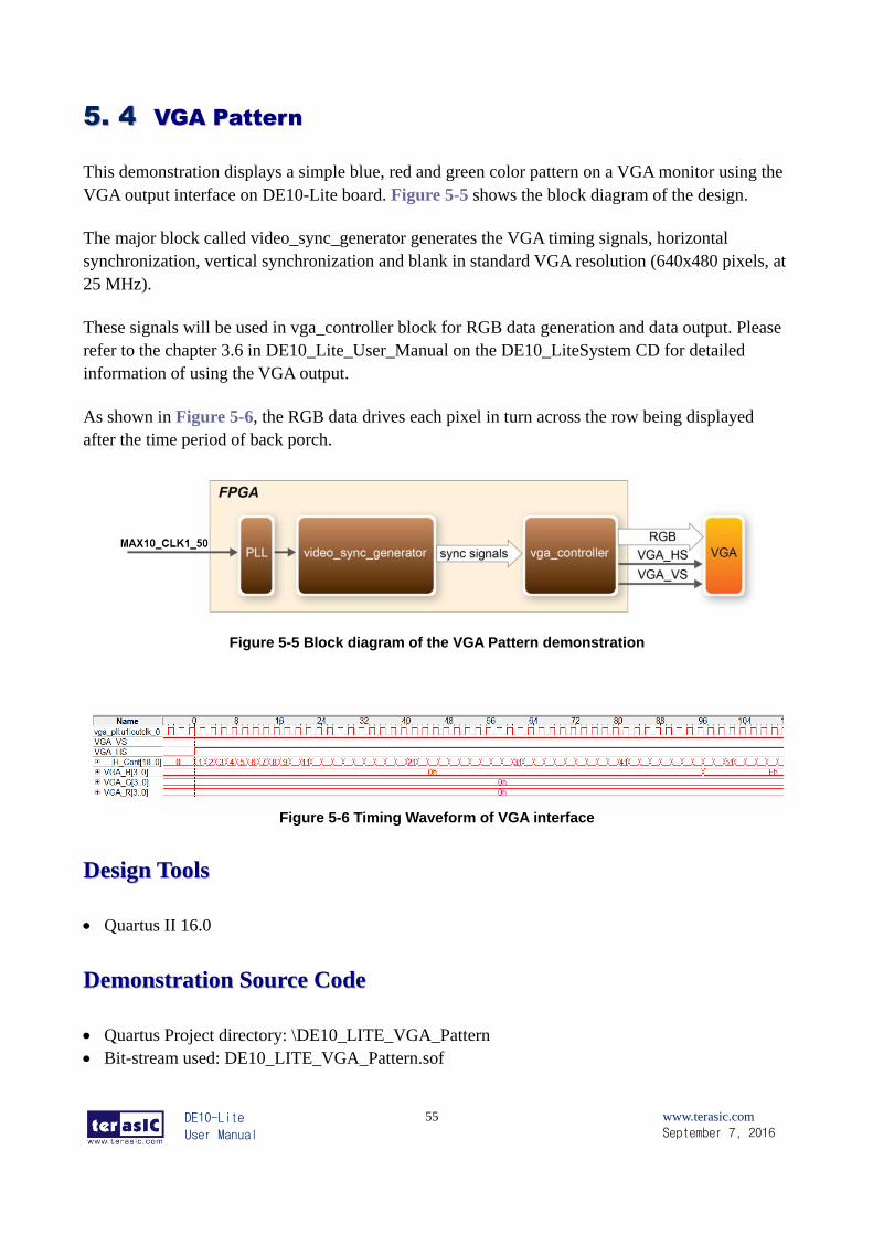
VGA output interface on DE10-Lite board. Figure 5-5 shows the block diagram of the design.
The major block called video_sync_generator generates the VGA timing signals, horizontal
synchronization, vertical synchronization and blank in standard VGA resolution (640x480 pixels, at
25 MHz).
These signals will be used in vga_controller block for RGB data generation and data output. Please
refer to the chapter 3.6 in DE10_Lite_User_Manual on the DE10_LiteSystem CD for detailed
information of using the VGA output.
As shown in Figure 5-6, the RGB data drives each pixel in turn across the row being displayed
after the time period of back porch.
Figure 5-5 Block diagram of the VGA Pattern demonstration
Figure 5-6 Timing Waveform of VGA interface
DDeessiiggnn TToooollss
Quartus II 16.0
DDeemmoonnssttrraattiioonn SSoouurrccee CCooddee
Quartus Project directory: \DE10_LITE_VGA_Pattern
Bit-stream used: DE10_LITE_VGA_Pattern.sof
DE10-Lite
User Manual
56
www.terasic.com
September 7, 2016
DDeemmoonnssttrraattiioonn BBaattcchh FFiillee
Demo Batch File Folder: \DE10_LITE_SD_DEMO\demo_batch\
The demo batch file includes following files:
Batch File for USB-Blaster: DE10_LITE_VGA_Pattern.bat
FPGA Configure File: DE10_LITE_VGA_Pattern.sof
DDeemmoonnssttrraattiioonn SSeettuupp
Quartus II v16.0 must be pre-installed to the host PC..
Connect the DE10-Lite board (J3) to the host PC with a USB cable and install the USB-Blaster
driver if necessary
Connect VGA D-SUB to a VGA monitor.
Execute the demo batch file “DE10_LITE_VGA_Pattern.bat” from the directory :
\ DE10_LITE_VGA_Pattern \demo_batch
The VGA monitor will display a color pattern.
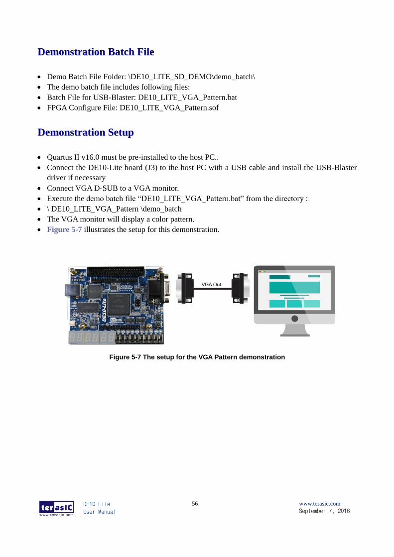
Figure 5-7 illustrates the setup for this demonstration.
Figure 5-7 The setup for the VGA Pattern demonstration
DE10-Lite
User Manual
57
www.terasic.com
September 7, 2016
55.. 55 GG--SSeennssoorr
This demonstration illustrates how to use the digital accelerometer on the DE10-Lite board to
measure the static acceleration of gravity in tilt-sensing applications. As the board is tilted from left
to right and right to left, the digital accelerometer detects the tilting movement and displays it on the
LEDs.
Function Block Diagram
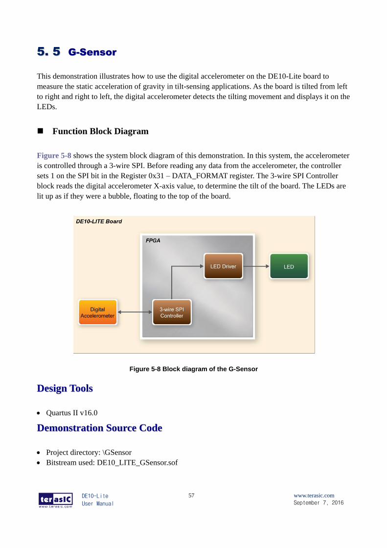
Figure 5-8 shows the system block diagram of this demonstration. In this system, the accelerometer
is controlled through a 3-wire SPI. Before reading any data from the accelerometer, the controller
sets 1 on the SPI bit in the Register 0x31 – DATA_FORMAT register. The 3-wire SPI Controller
block reads the digital accelerometer X-axis value, to determine the tilt of the board. The LEDs are
lit up as if they were a bubble, floating to the top of the board.
Figure 5-8 Block diagram of the G-Sensor
DDeessiiggnn TToooollss
Quartus II v16.0
DDeemmoonnssttrraattiioonn SSoouurrccee CCooddee
Project directory: \GSensor
Bitstream used: DE10_LITE_GSensor.sof
DE10-Lite
User Manual
58
www.terasic.com
September 7, 2016
DDeemmoonnssttrraattiioonn BBaattcchh FFiillee
Demo batch file folder: \GSensor\demo_batch
The directory includes the following files:
Batch file: test.bat
FPGA configuration file: DE10_LITE_GSensor.sof
DDeemmoonnssttrraattiioonn SSeettuupp
Quartus II v16.0 must be pre-installed to the host PC.
Connect the DE10-Lite board (J3) to the host PC with a USB cable and install the USB-Blaster
driver if necessary
Execute the demo batch file “test.bat” from the directory \GSensor\demo_batch. This will load
the demo into the FPGA.
Tilt the DE10-Lite board from side to side and observe the result on the LEDs.
DE10-Lite
User Manual
59
www.terasic.com
September 7, 2016
55.. 66 AADDCC MMeeaassuurreemmeenntt
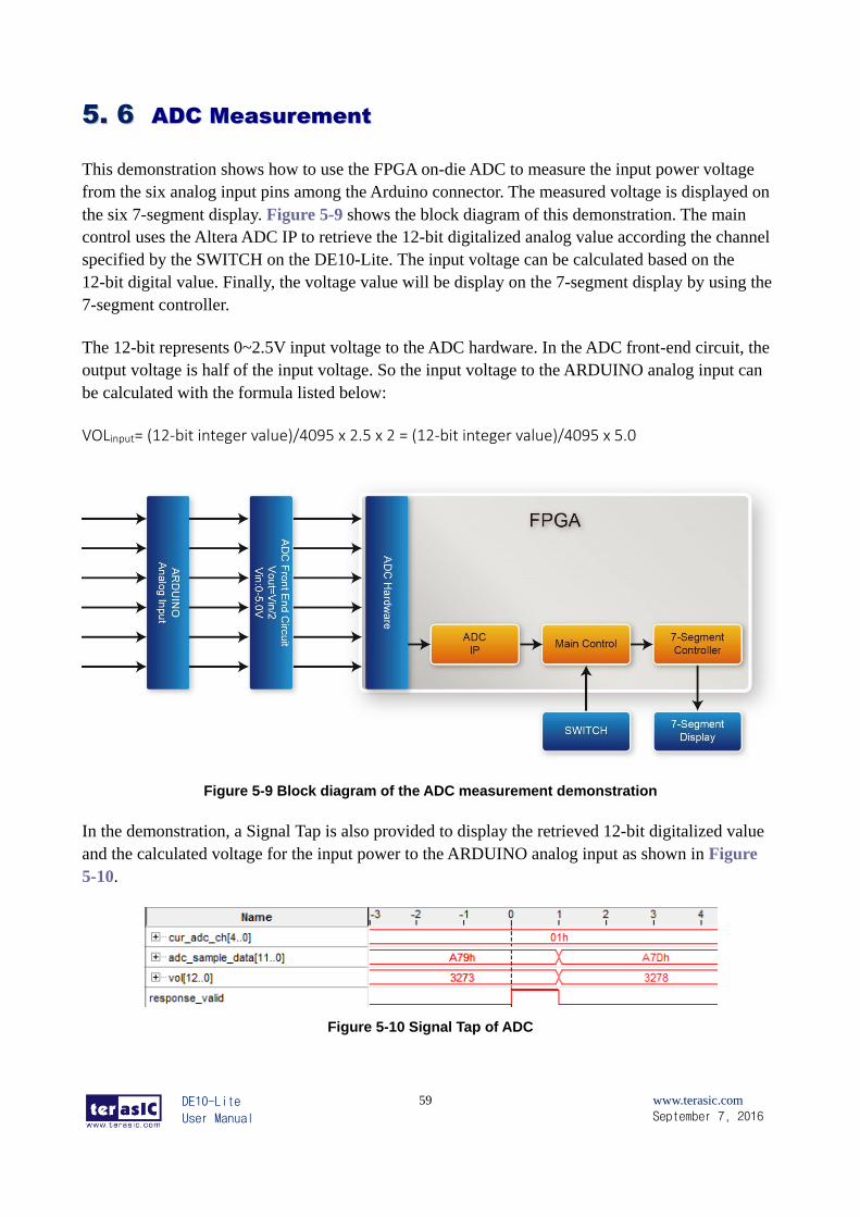
This demonstration shows how to use the FPGA on-die ADC to measure the input power voltage
from the six analog input pins among the Arduino connector. The measured voltage is displayed on
the six 7-segment display. Figure 5-9 shows the block diagram of this demonstration. The main
control uses the Altera ADC IP to retrieve the 12-bit digitalized analog value according the channel
specified by the SWITCH on the DE10-Lite. The input voltage can be calculated based on the
12-bit digital value. Finally, the voltage value will be display on the 7-segment display by using the
7-segment controller.
The 12-bit represents 0~2.5V input voltage to the ADC hardware. In the ADC front-end circuit, the
output voltage is half of the input voltage. So the input voltage to the ARDUINO analog input can
be calculated with the formula listed below:
VOLinput= (12-bit integer value)/4095 x 2.5 x 2 = (12-bit integer value)/4095 x 5.0
Figure 5-9 Block diagram of the ADC measurement demonstration
In the demonstration, a Signal Tap is also provided to display the retrieved 12-bit digitalized value
and the calculated voltage for the input power to the ARDUINO analog input as shown in Figure
5-10.
Figure 5-10 Signal Tap of ADC
DE10-Lite
User Manual
60
www.terasic.com
September 7, 2016
DDeessiiggnn TToooollss
Quartus II 16.0
DDeemmoonnssttrraattiioonn SSoouurrccee CCooddee
Quartus Project directory: ADC_RTL
Bitstream used: DE10_Lite.sof
DDeemmoonnssttrraattiioonn BBaattcchh FFiillee
Demo Batch File Folder: ADC_RTL \demo_batch\
The demo batch file includes following files:
Batch File for USB-Blaster: test.bat
FPGA Configure File: DE10_Lite.sof
DDeemmoonnssttrraattiioonn SSeettuupp
Quartus II 16.0 must be pre-installed to the host PC..
Connect USB Blaster to the DE10-Lite board and install USB Blaster driver if necessary.
Execute the demo batch file “test.bat” from the directory\ADC_RTL\demo_batch.
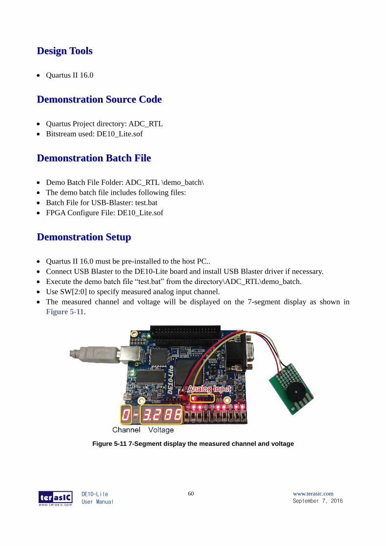
Use SW[2:0] to specify measured analog input channel.
The measured channel and voltage will be displayed on the 7-segment display as shown in
Figure 5-11.
Figure 5-11 7-Segment display the measured channel and voltage

DE10-Lite
User Manual
61
www.terasic.com
September 7, 2016
Additional Information
GGeettttiinngg HHeellpp
Here are the addresses where you can get help if you encounter problems:
Terasic Inc.
9F., No.176, Sec.2, Gongdao 5th Rd, East Dist, Hsinchu City, 30070. Taiwan
Email: [email protected]
Web: www.terasic.com
DE10-Lite Web: http://de10-lite.terasic.com/
RReevviissiioonn HHiissttoorryy
Date Version Change Log
2016.06 V1.0 Initial Version (Preliminary)
2016.09 V1.1 Minor corrections: fixing typos and change MAX 10 to production version.
CCooppyyrriigghhtt SSttaatteemmeenntt
Copyright © 2016 Terasic Inc. All rights reserved.