Embed Size (px)
Citation preview
1
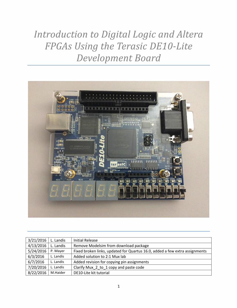
Introduction to Digital Logic and Altera FPGAs Using the Terasic DE10-Lite
Development Board
3/21/2016 L. Landis Initial Release
4/13/2016 L. Landis Remove Modelsim from download package
5/24/2016 P. Mayer Fixed broken links, updated for Quartus 16.0, added a few extra assignments
6/3/2016 L. Landis Added solution to 2:1 Mux lab
6/7/2016 L. Landis Added revision for copying pin assignments
7/20/2016 L. Landis Clarify Mux_2_to_1 copy and paste code
8/22/2016 M.Haider DE10-Lite kit tutorial
2
Lab 1: Obtaining the Quartus Prime Lite Design Tools
Background FPGAs are digital semiconductors that infinitely configurable and used to build a huge variety of electronic functions including Data Center accelerators, wireless base stations, and industrial motor controllers to name but a few of their common applications. An FPGA is a special type of semiconductor that can be reconfigured to perform different digital hardware functions so it makes for a great learning platform. To configure an FPGA you need to describe your digital electronics with either a Hardware Description Language (Verilog or VHDL are most common) or a schematic. Then you need to assign the “pins” of your FPGA based on how the printed circuit board connects the FPGA to various peripheral components on your board (switches, LEDS, memory devices and various connectors). Finally you will “compile” your design and program the FPGA to perform the function you have specified in the Hardware Description Language or schematic. The first step in this lab is to download the Altera design tools, called Quartus Prime Lite Edition. For the lower complexity Altera FPGA devices, the Quartus Prime Lite design tools are entirely free. Purchase here: http://www.terasic.com.tw/cgi-bin/page/archive.pl?Language=English&No=1021 and there are numerous labs and online trainings you can take based on this full featured kit. This training class assumes you have a very cursory knowledge of how computers and digital electronics work, but by no means do you need to be a degree electrical engineer to follow along this introductory course.
Installation Quartus Prime is Altera’s design tool suite. It serves a number of functions:
1. Design creation through the use of HDL languages or schematics
2. System creation through the Qsys graphical interface
3. Generation and editing of constraints: timing, pin locations, physical location on die, IO voltage
levels
4. Synthesis of high level language into an FPGA netlist (“mapping” in FPGA terminology)
5. FPGA place and route (“fitting” in FPGA terminology)
6. Generation of design image (used to program FPGA, “assembly” in FPGA terminology)
7. Timing Analysis
8. Programming/download of design image into FPGA hardware
9. Debugging by insertion of debug logic (in-chip logic analyzer)
10. Interfaces to 3rd party tools such as simulators
11. Launching of Software Build Tools (Eclipse) for Nios II
3
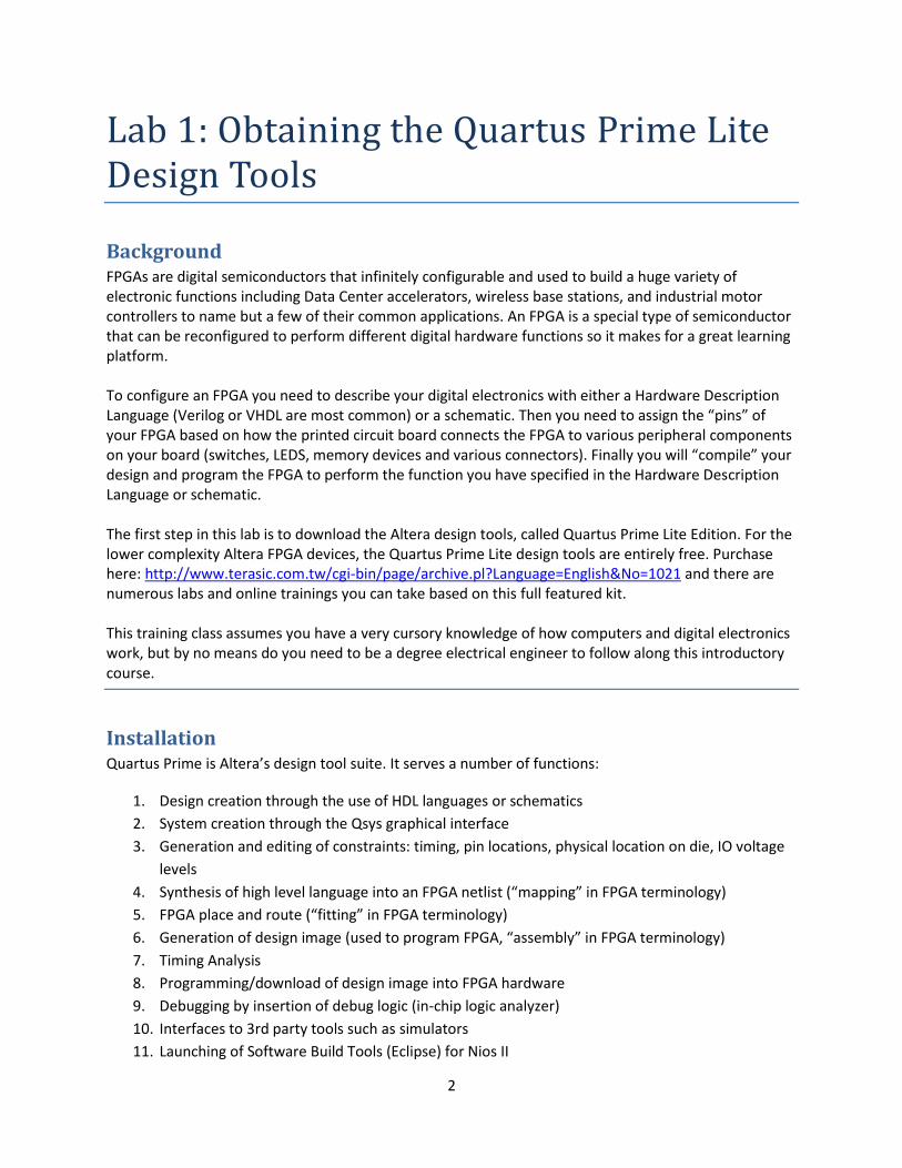
To download Quartus Prime Lite, follow these instructions: Visit this site: http://dl.altera.com/?edition=lite to download version 16.0 of Quartus Prime Lite. Select version 16.0 and your PC’s operating system. For the smallest installation, and quickest download time, enter only the entries shown below.
Figure 1: Quartus download page
Follow the instructions to download the Design Tools and you will have the Quartus Prime Lite version
16.0 tools up and running on your PC.
4
Lab 2: New Project Wizard
Summary This is a short lab that completes the basic project setup. At the end of this lab, you will be able to start a
new project using New Project Wizard in Quartus Prime Software. There are other related tutorial links
provided for you to learn more about the software.
Lab Instruction
2.0
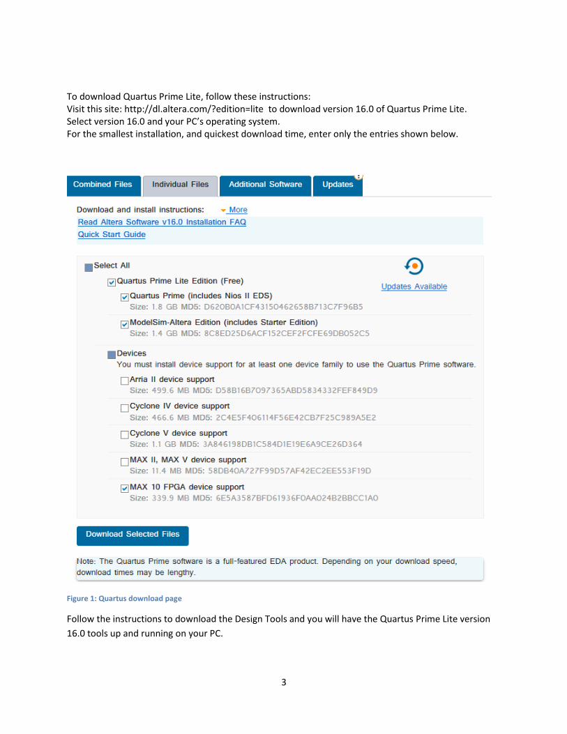
Open the tools by double clicking the “Quartus Prime” icon.
You should now see something similar to the image below. The function for each panel is listed below.
Project Navigator Tool View Window
IP Catalog
Tcl Console Window
Message Window
5
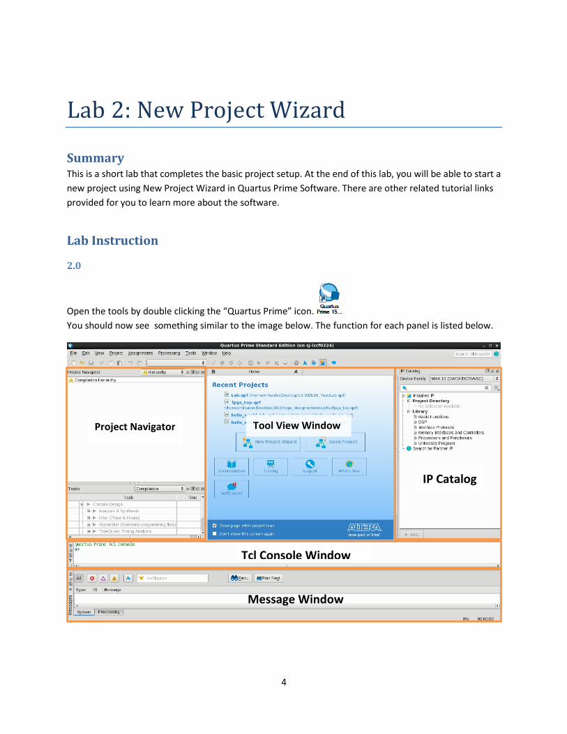
2.1 Select File -> New Project Wizard
Pane 1: Basics. Fill in with a directory of your choice. It is recommended to be a personal directory, and
not a directory under the Quartus installation which is the default. Call the project Lab and the top level
entity Switch_to_LED. Note that the screen shots will have a different directory than what you will use
for your project. This is fine.
2.2
Pane 2: Project Type. Select Empty project.
2.3
Pane 3: Source Files. Click Next. We will add project source files later.
2.4
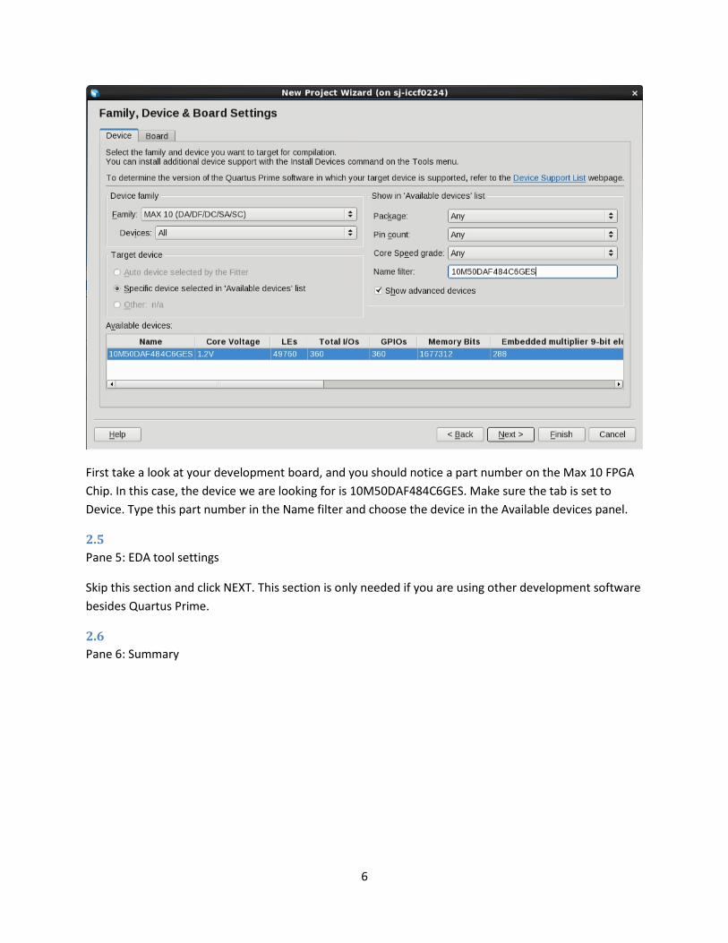
Pane 4: Family & Device Settings
6
First take a look at your development board, and you should notice a part number on the Max 10 FPGA
Chip. In this case, the device we are looking for is 10M50DAF484C6GES. Make sure the tab is set to
Device. Type this part number in the Name filter and choose the device in the Available devices panel.
2.5
Pane 5: EDA tool settings
Skip this section and click NEXT. This section is only needed if you are using other development software
besides Quartus Prime.
2.6
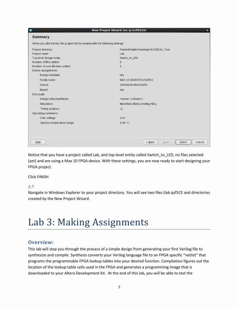
Pane 6: Summary
7
Notice that you have a project called Lab, and top-level entity called Switch_to_LED, no files selected
(yet) and are using a Max 10 FPGA device. With these settings, you are now ready to start designing your
FPGA project.
Click FINISH
2.7
Navigate in Windows Explorer to your project directory. You will see two files (lab.qsf5CE and directories
created by the New Project Wizard.
Lab 3: Making Assignments
Overview: This lab will step you through the process of a simple design from generating your first Verilog file to
synthesize and compile. Synthesis converts your Verilog language file to an FPGA specific “netlist” that
programs the programmable FPGA lookup tables into your desired function. Compilation figures out the
location of the lookup table cells used in the FPGA and generates a programming image that is
downloaded to your Altera Development kit. At the end of this lab, you will be able to test the
8
functionality of the example digital electronic circuits by toggling the switches and observing the LEDs
for proper circuit operation.
Instruction:
3.1
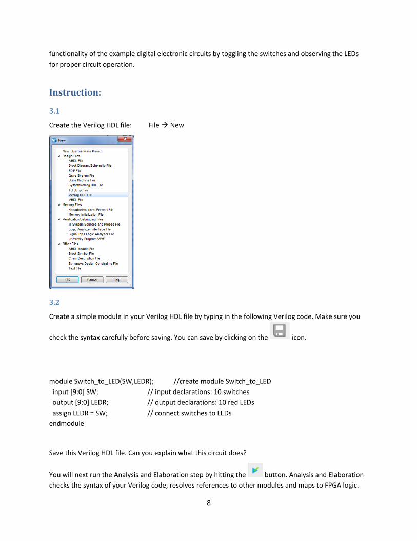
Create the Verilog HDL file: File New
3.2
Create a simple module in your Verilog HDL file by typing in the following Verilog code. Make sure you
check the syntax carefully before saving. You can save by clicking on the icon.
module Switch_to_LED(SW,LEDR); //create module Switch_to_LED
input [9:0] SW; // input declarations: 10 switches
output [9:0] LEDR; // output declarations: 10 red LEDs
assign LEDR = SW; // connect switches to LEDs
endmodule
Save this Verilog HDL file. Can you explain what this circuit does?
You will next run the Analysis and Elaboration step by hitting the button. Analysis and Elaboration
checks the syntax of your Verilog code, resolves references to other modules and maps to FPGA logic.
9
The next step is Fitting, which assigns the Lookup tables to physical locations on your FPGA chip, and
Assembly which generates the image file to program your FPGA. If you see any errors during the Analysis
and Elaboration step, carefully review your Verilog code for syntax errors and re-run this step.
3.3
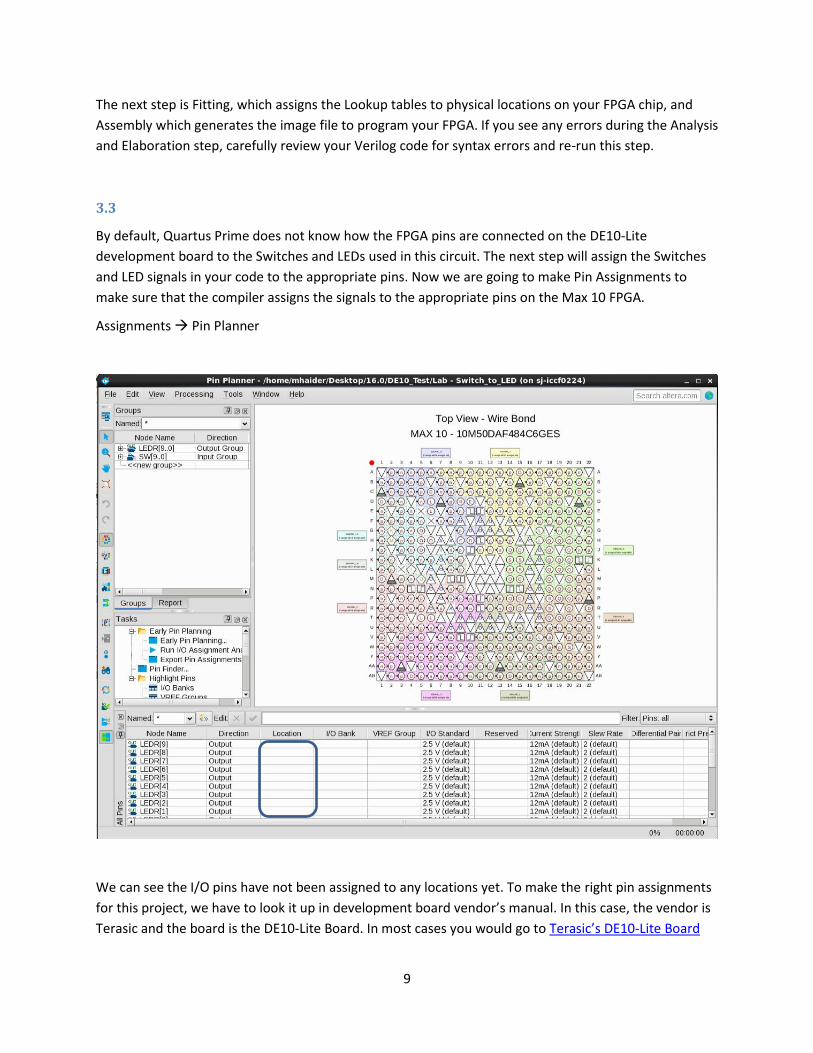
By default, Quartus Prime does not know how the FPGA pins are connected on the DE10-Lite
development board to the Switches and LEDs used in this circuit. The next step will assign the Switches
and LED signals in your code to the appropriate pins. Now we are going to make Pin Assignments to
make sure that the compiler assigns the signals to the appropriate pins on the Max 10 FPGA.
Assignments Pin Planner
We can see the I/O pins have not been assigned to any locations yet. To make the right pin assignments
for this project, we have to look it up in development board vendor’s manual. In this case, the vendor is
Terasic and the board is the DE10-Lite Board. In most cases you would go to Terasic’s DE10-Lite Board
10
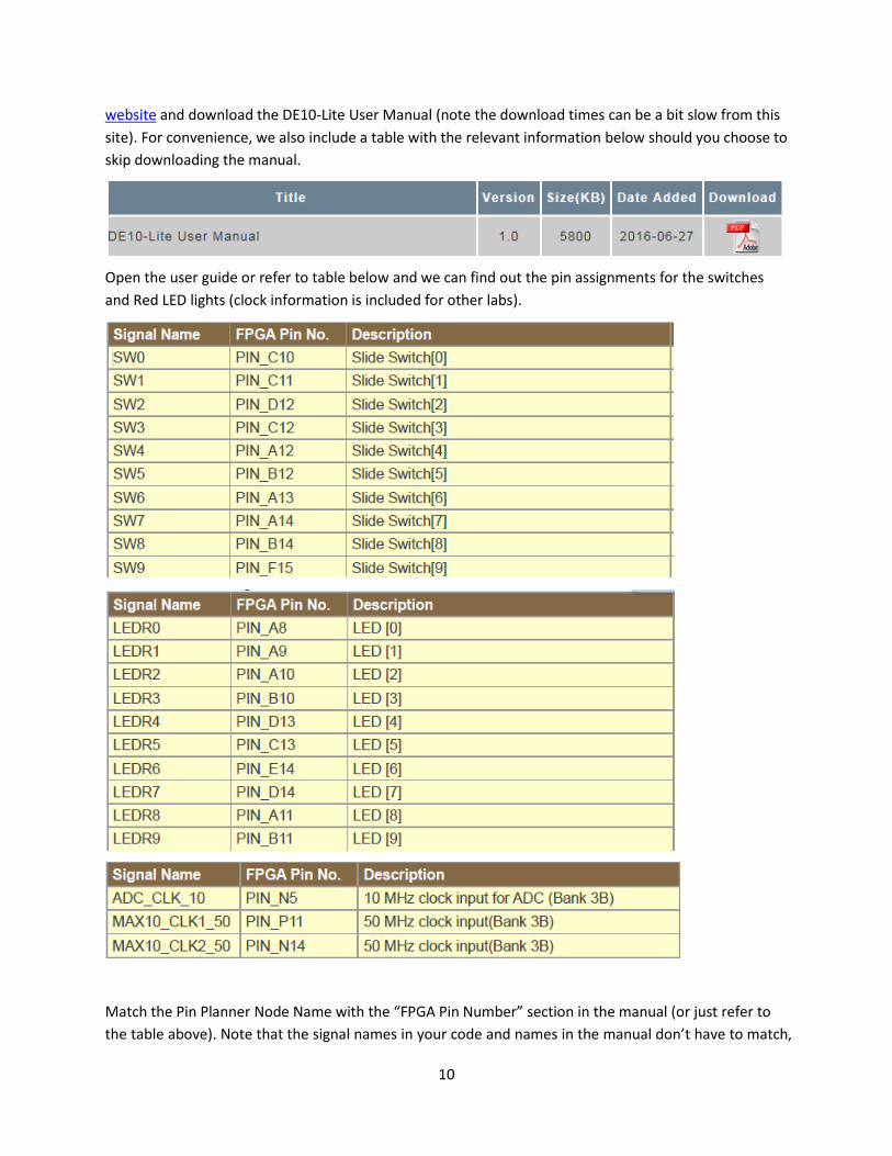
website and download the DE10-Lite User Manual (note the download times can be a bit slow from this
site). For convenience, we also include a table with the relevant information below should you choose to
skip downloading the manual.
Open the user guide or refer to table below and we can find out the pin assignments for the switches
and Red LED lights (clock information is included for other labs).
Match the Pin Planner Node Name with the “FPGA Pin Number” section in the manual (or just refer to
the table above). Note that the signal names in your code and names in the manual don’t have to match,
11
as long as you connect to the proper pin location, your design will be connected properly. Enter a few of
the pin locations using this method of typing in the location in the Pin Planner application. An alternate
method is to left click on the node name and drag the pin on top of the ball grid map location that is
assigned in the table. Release the pin on the proper location. Hit the escape key and move to the next
pin.
When you finish, you can just close the window – the Planner does not have a Save button, but it will
save anyways. Note that it is possible to “preload” the Signal locations from the board through a
different means, but we want to highlight that Quartus Prime needs to be instructed how signals are
associated with pins connected on the development board. This switch to LED lab does not require the
CLOCK signals so you can ignore these for the time being.
3.4
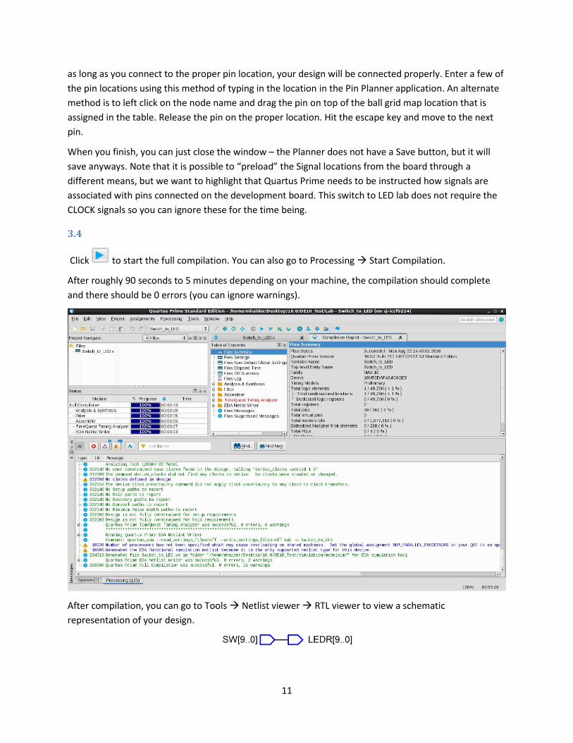
Click to start the full compilation. You can also go to Processing Start Compilation.
After roughly 90 seconds to 5 minutes depending on your machine, the compilation should complete
and there should be 0 errors (you can ignore warnings).
After compilation, you can go to Tools Netlist viewer RTL viewer to view a schematic
representation of your design.
12
3.5
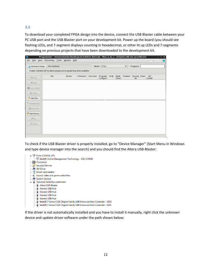
To download your completed FPGA design into the device, connect the USB Blaster cable between your
PC USB port and the USB Blaster port on your development kit. Power up the board (you should see
flashing LEDs, and 7-segment displays counting in hexadecimal, or other lit up LEDs and 7-segments
depending on previous projects that have been downloaded to the development kit.
.
To check if the USB Blaster driver is properly installed, go to “Device Manager” (Start Menu in Windows
and type device manager into the search) and you should find the Altera USB-Blaster:
If the driver is not automatically installed and you have to install it manually, right click the unknown
device and update driver software under the path shown below:
13
3.6
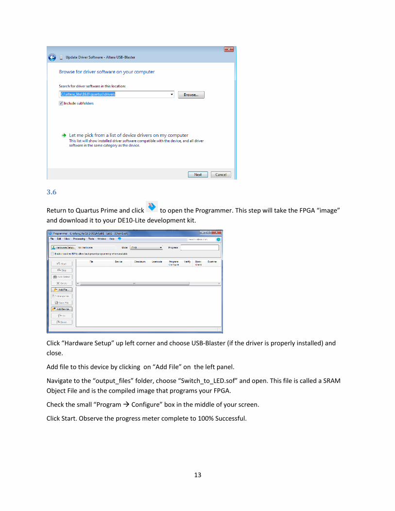
Return to Quartus Prime and click to open the Programmer. This step will take the FPGA “image”
and download it to your DE10-Lite development kit.
Click “Hardware Setup” up left corner and choose USB-Blaster (if the driver is properly installed) and
close.
Add file to this device by clicking on “Add File” on the left panel.
Navigate to the “output_files” folder, choose “Switch_to_LED.sof” and open. This file is called a SRAM
Object File and is the compiled image that programs your FPGA.
Check the small “Program Configure” box in the middle of your screen.
Click Start. Observe the progress meter complete to 100% Successful.
14
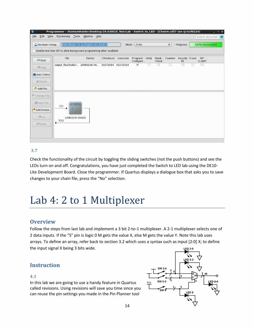
3.7
Check the functionality of the circuit by toggling the sliding switches (not the push buttons) and see the
LEDs turn on and off. Congratulations, you have just completed the Switch to LED lab using the DE10-
Lite Development Board. Close the programmer. If Quartus displays a dialogue box that asks you to save
changes to your chain file, press the “No” selection.
Lab 4: 2 to 1 Multiplexer
Overview Follow the steps from last lab and implement a 3 bit 2-to-1 multiplexer. A 2-1 multiplexer selects one of
2 data inputs. If the “S” pin is logic 0 M gets the value X, else M gets the value Y. Note this lab uses
arrays. To define an array, refer back to section 3.2 which uses a syntax such as input [2:0] X; to define
the input signal X being 3 bits wide.
Instruction
4.1
In this lab we are going to use a handy feature in Quartus called revisions. Using revisions will save you time since you can reuse the pin settings you made in the Pin Planner tool
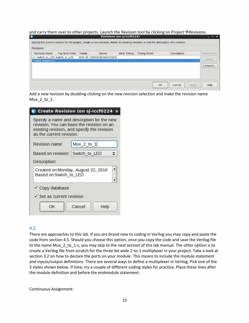
15
and carry them over to other projects. Launch the Revision tool by clicking on ProjectRevisions.
Add a new revision by doubling clicking on the new revision selection and make the revision name Mux_2_to_1.
4.2
There are approaches to this lab. If you are brand new to coding in Verilog you may copy and paste the code from section 4.5. Should you choose this option, once you copy the code and save the Verilog file to the name Mux_2_to_1.v, you may skip to the next section of this lab manual. The other option is to create a Verilog file from scratch for the three-bit wide 2-to-1 multiplexer in your project. Take a look at section 3.2 on how to declare the ports on your module. This means to include the module statement and inputs/output definitions. There are several ways to define a multiplexer in Verilog. Pick one of the 3 styles shown below. If time, try a couple of different coding styles for practice. Place these lines after the module definition and before the endmodule statement. Continuous Assignment:
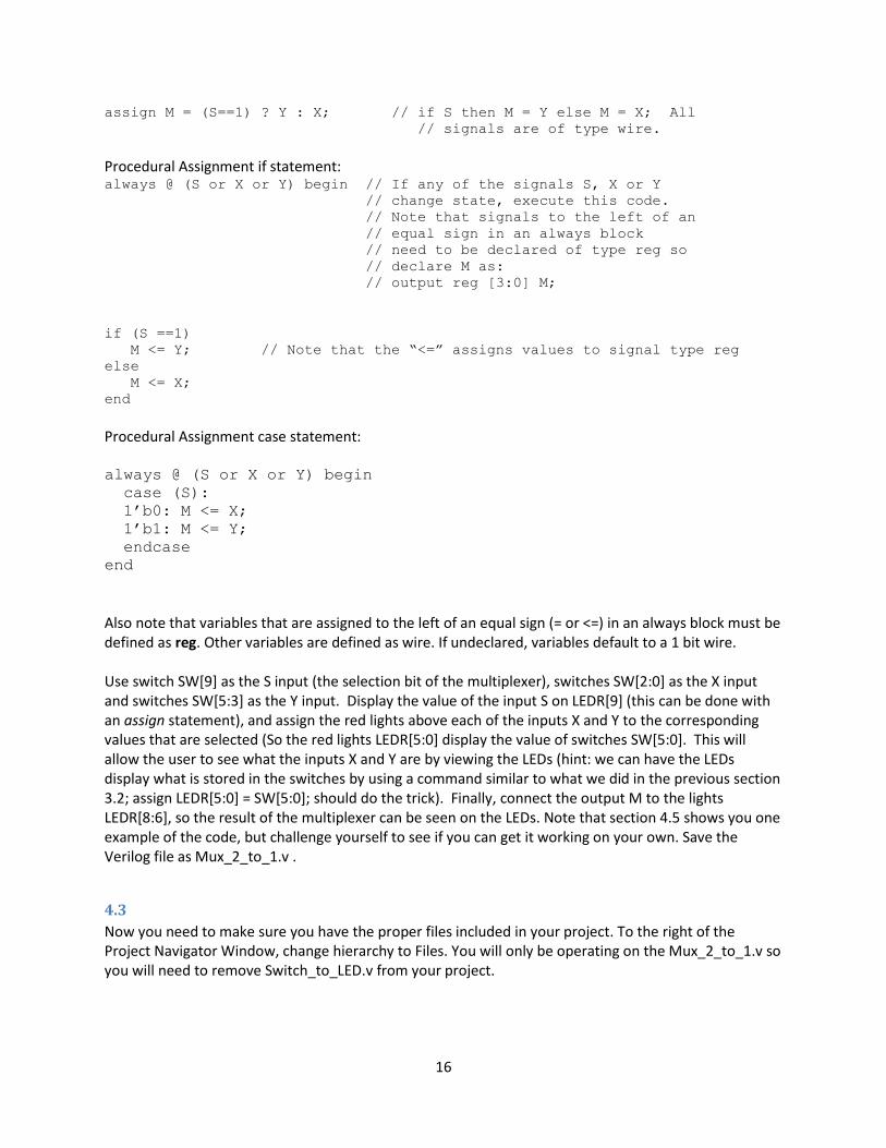
16
assign M = (S==1) ? Y : X; // if S then M = Y else M = X; All
// signals are of type wire.
Procedural Assignment if statement: always @ (S or X or Y) begin // If any of the signals S, X or Y
// change state, execute this code.
// Note that signals to the left of an
// equal sign in an always block
// need to be declared of type reg so
// declare M as:
// output reg [3:0] M;
if (S ==1)
M <= Y; // Note that the “<=” assigns values to signal type reg
else
M <= X;
end
Procedural Assignment case statement: always @ (S or X or Y) begin
case (S):
1’b0: M <= X;
1’b1: M <= Y;
endcase
end
Also note that variables that are assigned to the left of an equal sign (= or <=) in an always block must be defined as reg. Other variables are defined as wire. If undeclared, variables default to a 1 bit wire. Use switch SW[9] as the S input (the selection bit of the multiplexer), switches SW[2:0] as the X input and switches SW[5:3] as the Y input. Display the value of the input S on LEDR[9] (this can be done with an assign statement), and assign the red lights above each of the inputs X and Y to the corresponding values that are selected (So the red lights LEDR[5:0] display the value of switches SW[5:0]. This will allow the user to see what the inputs X and Y are by viewing the LEDs (hint: we can have the LEDs display what is stored in the switches by using a command similar to what we did in the previous section 3.2; assign LEDR[5:0] = SW[5:0]; should do the trick). Finally, connect the output M to the lights LEDR[8:6], so the result of the multiplexer can be seen on the LEDs. Note that section 4.5 shows you one example of the code, but challenge yourself to see if you can get it working on your own. Save the Verilog file as Mux_2_to_1.v .
4.3
Now you need to make sure you have the proper files included in your project. To the right of the Project Navigator Window, change hierarchy to Files. You will only be operating on the Mux_2_to_1.v so you will need to remove Switch_to_LED.v from your project.
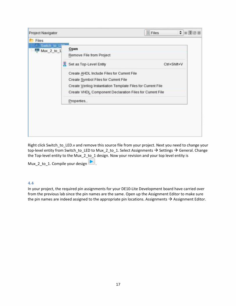
17
Right click Switch_to_LED.v and remove this source file from your project. Next you need to change your top-level entity from Switch_to_LED to Mux_2_to_1. Select Assignments Settings General. Change the Top-level entity to the Mux_2_to_1 design. Now your revision and your top level entity is
Mux_2_to_1. Compile your design .
4.4
In your project, the required pin assignments for your DE10-Lite Development board have carried over from the previous lab since the pin names are the same. Open up the Assignment Editor to make sure the pin names are indeed assigned to the appropriate pin locations. Assignments Assignment Editor.
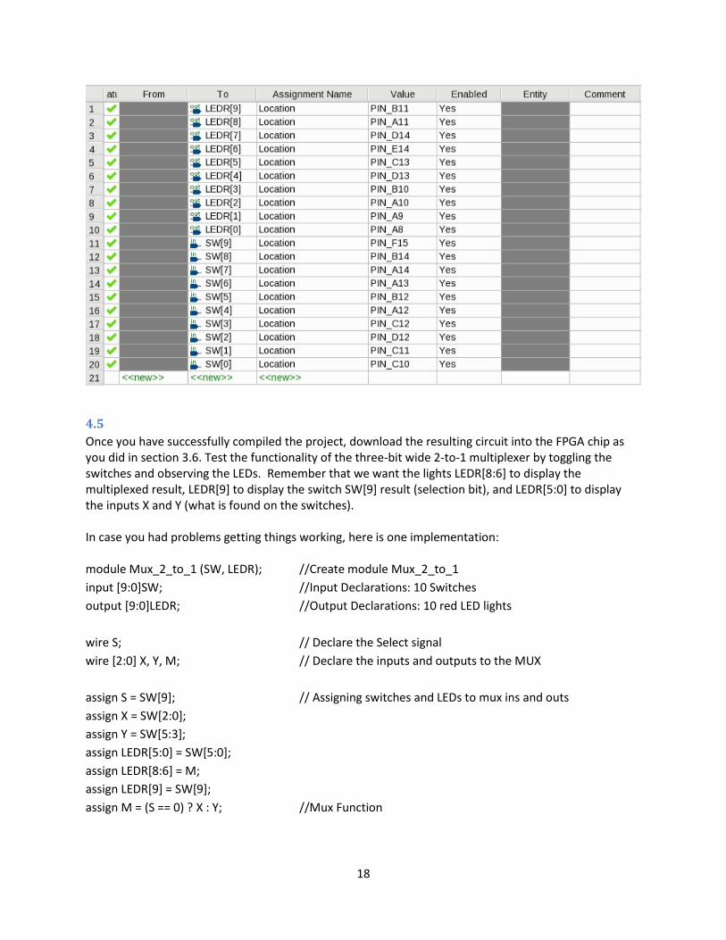
18
4.5
Once you have successfully compiled the project, download the resulting circuit into the FPGA chip as you did in section 3.6. Test the functionality of the three-bit wide 2-to-1 multiplexer by toggling the switches and observing the LEDs. Remember that we want the lights LEDR[8:6] to display the multiplexed result, LEDR[9] to display the switch SW[9] result (selection bit), and LEDR[5:0] to display the inputs X and Y (what is found on the switches). In case you had problems getting things working, here is one implementation: module Mux_2_to_1 (SW, LEDR); //Create module Mux_2_to_1
input [9:0]SW; //Input Declarations: 10 Switches
output [9:0]LEDR; //Output Declarations: 10 red LED lights
wire S; // Declare the Select signal
wire [2:0] X, Y, M; // Declare the inputs and outputs to the MUX
assign S = SW[9]; // Assigning switches and LEDs to mux ins and outs
assign X = SW[2:0];
assign Y = SW[5:3];
assign LEDR[5:0] = SW[5:0];
assign LEDR[8:6] = M;
assign LEDR[9] = SW[9];
assign M = (S == 0) ? X : Y; //Mux Function
19
endmodule
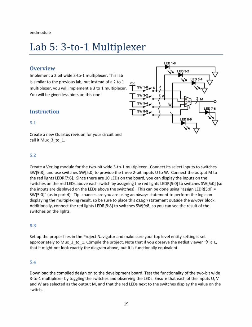
Lab 5: 3-to-1 Multiplexer
Overview Implement a 2 bit wide 3-to-1 multiplexer. This lab
is similar to the previous lab, but instead of a 2 to 1
multiplexer, you will implement a 3 to 1 multiplexer.
You will be given less hints on this one!
Instruction
5.1
Create a new Quartus revision for your circuit and call it Mux_3_to_1.
5.2
Create a Verilog module for the two-bit wide 3-to-1 multiplexer. Connect its select inputs to switches SW[9:8], and use switches SW[5:0] to provide the three 2-bit inputs U to W. Connect the output M to the red lights LEDR[7:6]. Since there are 10 LEDs on the board, you can display the inputs on the switches on the red LEDs above each switch by assigning the red lights LEDR[5:0] to switches SW[5:0] (so the inputs are displayed on the LEDs above the switches). This can be done using “assign LEDR[5:0] = SW[5:0]” (as in part 4). Tip: chances are you are using an always statement to perform the logic on displaying the multiplexing result, so be sure to place this assign statement outside the always block. Additionally, connect the red lights LEDR[9:8] to switches SW[9:8] so you can see the result of the switches on the lights.
5.3
Set up the proper files in the Project Navigator and make sure your top level entity setting is set appropriately to Mux_3_to_1. Compile the project. Note that if you observe the netlist viewer RTL, that it might not look exactly the diagram above, but it is functionally equivalent.
5.4
Download the compiled design on to the development board. Test the functionality of the two-bit wide 3-to-1 multiplexer by toggling the switches and observing the LEDs. Ensure that each of the inputs U, V and W are selected as the output M, and that the red LEDs next to the switches display the value on the switch.
20
Lab 6: Knight Rider
Perhaps some of you have heard of or watched a TV show called Knight Rider that aired from 1982 to
1986 and starred David Hasselhoff. The premise of the show was David Hasselhoff was a high tech crime
fighter (at least high technology for 1982) and drove around an intelligent car named “KITT”. The KITT
car was a 1982 Pontiac Trans-Am sports car with all sorts of cool gadgets. The interesting gadget of
interest for this lab were the headlights of KITT which consisted of a horizontal bar of lights that
sequenced one at a time from left to right and back again at the rate of about 1/10th of a second per
light. Check out this short youtube1 video for crime fighting and automotive lighting technology’s finest
moment. This lab will teach you a thing or two about sequential logic and flip-flops. Let’s quickly review
how flip-flops work.
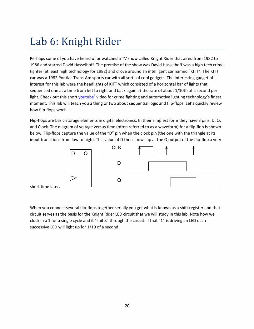
Flip-flops are basic storage elements in digital electronics. In their simplest form they have 3 pins: D, Q,
and Clock. The diagram of voltage versus time (often referred to as a waveform) for a flip-flop is shown
below. Flip-flops capture the value of the “D” pin when the clock pin (the one with the triangle at its
input transitions from low to high). This value of D then shows up at the Q output of the flip-flop a very
short time later.
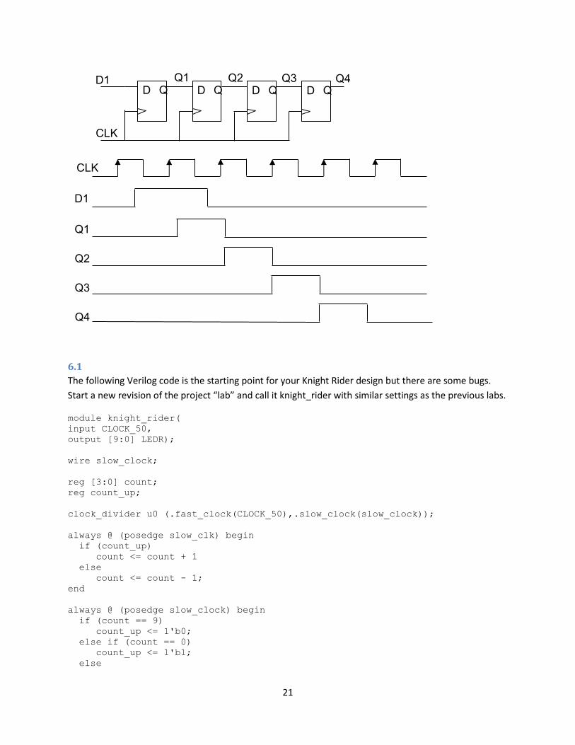
When you connect several flip-flops together serially you get what is known as a shift register and that
circuit serves as the basis for the Knight Rider LED circuit that we will study in this lab. Note how we
clock in a 1 for a single cycle and it “shifts” through the circuit. If that “1” is driving an LED each
successive LED will light up for 1/10 of a second.
D Q
D
Q
CLK
21
6.1
The following Verilog code is the starting point for your Knight Rider design but there are some bugs.
Start a new revision of the project “lab” and call it knight_rider with similar settings as the previous labs.
module knight_rider(
input CLOCK_50,
output [9:0] LEDR);
wire slow_clock;
reg [3:0] count;
reg count_up;
clock_divider u0 (.fast_clock(CLOCK_50),.slow_clock(slow_clock));
always @ (posedge slow_clk) begin
if (count_up)
count <= count + 1
else
count <= count - 1;
end
always @ (posedge slow_clock) begin
if (count == 9)
count_up <= 1'b0;
else if (count == 0)
count_up <= 1'b1;
else
D Q D Q D Q D Q D1
CLK
Q1 Q2 Q3 Q4
CLK
D1
Q1
Q2
Q3
Q4
22
count_up <= count_up;
end
assign led[9:0] = (1'b1 << count);
endmodule
module clock_divider(
input fast_clock,
output slow_clock);
parameter COUNTER_SIZE = 5;
parameter COUNTER_MAX_COUNT = (2 ** COUNTER_SIZE) - 1;
reg [COUNTER_SIZE-1:0] count;
always @(posedge fast_clock)
begin
if(count==COUNTER_MAX_COUNT)
count<=0;
else
count<=count+1;
end
assign slow_clock = count[COUNTER_SIZE-1];
endmodule
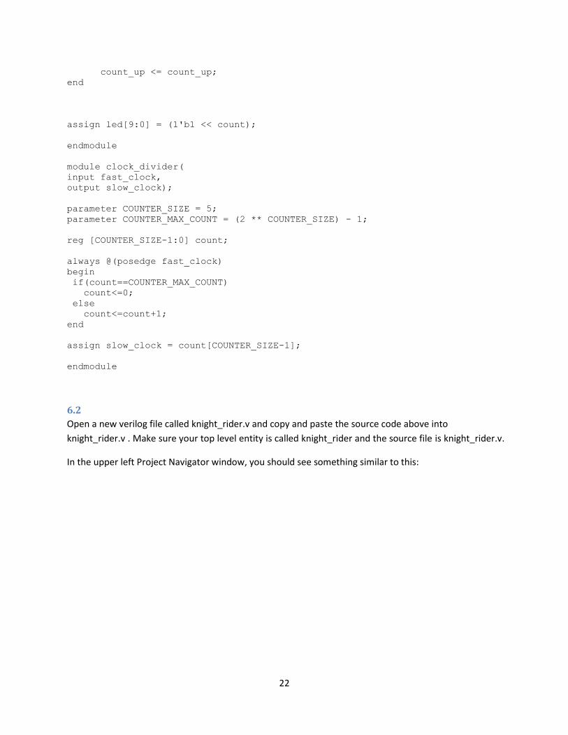
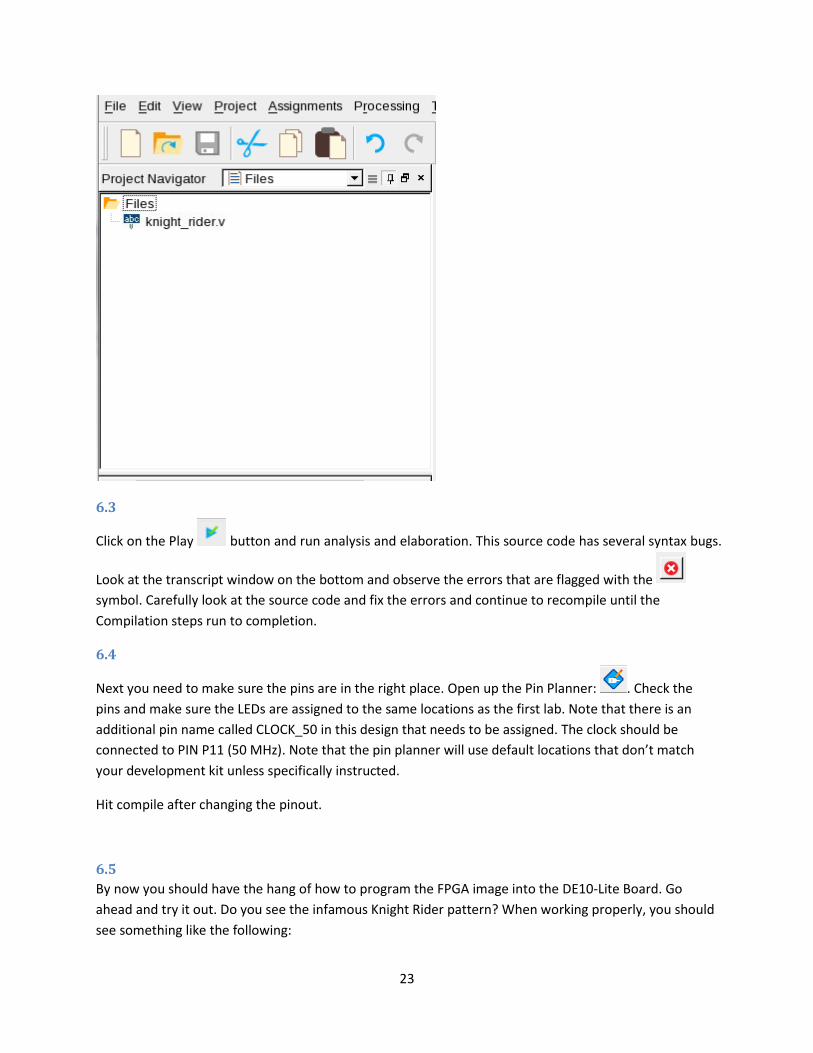
6.2
Open a new verilog file called knight_rider.v and copy and paste the source code above into
knight_rider.v . Make sure your top level entity is called knight_rider and the source file is knight_rider.v.
In the upper left Project Navigator window, you should see something similar to this:
23
6.3
Click on the Play button and run analysis and elaboration. This source code has several syntax bugs.
Look at the transcript window on the bottom and observe the errors that are flagged with the
symbol. Carefully look at the source code and fix the errors and continue to recompile until the
Compilation steps run to completion.
6.4
Next you need to make sure the pins are in the right place. Open up the Pin Planner: . Check the
pins and make sure the LEDs are assigned to the same locations as the first lab. Note that there is an
additional pin name called CLOCK_50 in this design that needs to be assigned. The clock should be
connected to PIN P11 (50 MHz). Note that the pin planner will use default locations that don’t match
your development kit unless specifically instructed.
Hit compile after changing the pinout.
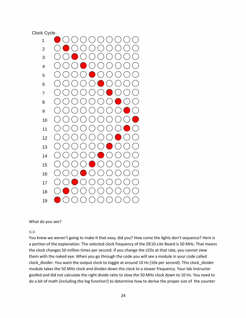
6.5
By now you should have the hang of how to program the FPGA image into the DE10-Lite Board. Go
ahead and try it out. Do you see the infamous Knight Rider pattern? When working properly, you should
see something like the following:
24
What do you see?
6.6
You knew we weren’t going to make it that easy, did you? How come the lights don’t sequence? Here is
a portion of the explanation. The selected clock frequency of the DE10-Lite Board is 50 MHz. That means
the clock changes 50 million times per second. If you change the LEDs at that rate, you cannot view
them with the naked eye. When you go through the code you will see a module in your code called
clock_divider. You want the output clock to toggle at around 10 Hz (10x per second). This clock_divider
module takes the 50 MHz clock and divides down the clock to a slower frequency. Your lab instructor
goofed and did not calculate the right divide ratio to slow the 50 MHz clock down to 10 Hz. You need to
do a bit of math (including the log function!) to determine how to derive the proper size of the counter
1
2
3
4
5
6
7
8
9
10
11
12
13
14
15
16
17
18
19
Clock Cycle

25
to divide 50 MHz to roughly 10 Hz. Basically, think about a divide ratio that is 2^N where N is the width
of the counter. Adjust the parameter to COUNTER_SIZE to the appropriate ratio and recompile and
reprogram the FPGA. Work out N based on the following equation: 10 = 50,000,000 / 2^N. Round N up
to the nearest integer to discover the proper WIDTH parameter setting. Recompile and program the
DE10-Lite development board.
6.7
Is the knight rider sequence working properly? Does each LED stay on for ~1/10 second? If not, redo
your math to find the right WIDTH parameter. Look at the sequencing carefully. Does each LED
illuminate once and proceed to its neighboring LED? As you will observe, the LED[0] and LED[9] blink
twice. Dang – that lab instructor created another error in the design! Look at the source code in the
knight_rider.v code and see if you can find the error. Change the code, recompile and reprogram your
DE10-Lite development kit until your Knight Rider LEDs are sequencing properly.
Thanks for taking time learning how to develop Altera FPGA products. We hope you found this lab
informative. Long live David Hasselhoff2!
1. https://www.youtube.com/watch?v=Mo8Qls0HnWo
2. https://www.youtube.com/watch?v=PJQVlVHsFF8