Embed Size (px)
Citation preview

DDC/DUC Fundamentals Application Note Page 1 of 60
DIGITAL DOWN/UP CONVERTERS FUNDAMENTALS
TEXAS INSTRUMENTS - WIRELESS RADIO PRODUCTS GROUP Joe Quintal
DDC/DUC Fundamentals Application Note Page 2 of 60
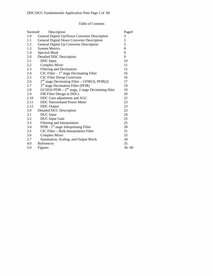
Table of Contents Section# Description Page# 1.0 General Digital Up/Down Converter Description 3 1.1 General Digital Down Converter Description 3 1.2 General Digital Up Converter Description 5 1.3 System Metrics 8 1.4 Spectral Mask 9 2.0 Detailed DDC Description 9 2.1 DDC Input 10 2.2 Complex Mixer 11 2.3 Filtering and Decimation 12 2.4 CIC Filter – 1st stage Decimating Filter 16 2.5 CIC Filter Droop Correction 16 2.6 2nd stage Decimating Filter – CFIR(3), PFIR(2) 17 2.7 3rd stage Decimation Filter (PFIR) 19 2.8 GC5016 PFIR – 2nd stage, 2 stage Decimating filter 19 2.9 FIR Filter Design in DDCs 20 2.10 DDC Gain adjustment and AGC 22 2.11 DDC Narrowband Power Meter 23 2.12 DDC Output 23 3.0 Detailed DUC Description 23 3.1 DUC Input 24 3.2 DUC Input Gain 25 3.3 Filtering and Interpolation 25 3.4 PFIR - 1st stage Interpolating Filter 28 3.5 CIC Filter – Bulk Interpolation Filter 31 3.6 Complex Mixer 33 3.7 Summation, Scaling, and Output Block 34 4.0 References 35 5.0 Figures 36- 60
DDC/DUC Fundamentals Application Note Page 3 of 60
1.0 General Digital Up/Down Converter Description TI Wireless Radio Products devices provide digital signal processing functions for digital receiver, transmitter, and filtering functions. This application note describes the Digital Down Converter (DDC) and Digital Up Converter (DUC) fundamentals, and compares current products. The DDC provides signal selection, frequency translation, filtering, and decimation of digital input signals, and gives a baseband complex output. The DUC provides interpolation, filtering, frequency translation, and summing of DUC channel outputs to produce digital IF outputs. DDCs can be found in wireless basestation receive electronics, specialized digital IF transmit-test equipment, and software defined receive-radio equipment. The number of DDC channels is based on the number of frequency carriers, number of phased or diverse antennas, and antenna delay calibration inputs. DUCs can be found in wireless basestation transmit electronics, specialized digital IF receive-test equipment, cable TV modulators, and software defined transmit-radio equipment. The number of DUC channels is based on the number of frequency carriers, number of phased or diverse antennas, and antenna delay calibration outputs. Repeaters have one or two receive sections, and one or two transmit sections. Repeaters and smaller capacity basestations can have 2 or 4 DDC and DUC channels. Test equipment and digital radio electronics typically use DDC and DUC devices combined with ADC and DAC to provide digital radio sections, or other specific applications such as receiver/transmitter test equipment. 1.1 General Digital Down Converter (DDC) Description This section introduces the component blocks of the DDC. More detailed discussion can be found in Section 2. An example of a digital Intermediate Frequency (IF) subsystem with DDC block diagram is shown in figure 1. The IF bandpass filter provides filtering for the IF amplifier. It has a digital gain control which is used to amplify the analog IF signal. An anti-aliasing low pass filter provides bandlimiting of the analog input signal for the A/D converter. The A/D converter samples the analog signal and provides a 2s complement digital output. The clock source provides a high-quality sample clock for the A/D converter, and an Rx clock for the DDC. General DDC functions are to translate frequency, filter, decimate the sample rate, adjust the narrowband gain, and output complex baseband signals. A DDC channel demodulates a band of frequencies from mixer frequency – ½ complex output bandwidth to the mixer frequency + ½ complex output bandwidth. The DDC input can be real or complex. The DDC input ports are mapped based on the real or
Comment [ah1]:
Comment [ah2]: Receiver?
Comment [ah3]: Transmitter?
DDC/DUC Fundamentals Application Note Page 4 of 60
complex format to a DDC channel input. It translates the desired IF input to 0Hz (baseband). Decimating filters provide filtering and reduce the output sample rate. The DDC output can be output as a single channel or combined with other channels in a Time Division Multiplexed (TDM) output format. The DDC output to demod interface converts the DDC baseband output to the signal format for the baseband demodulator. The baseband demodulator converts the baseband IQ signals to user data and signal statistics. A DDC Block Diagram is shown in Figures 2a and 2b. Figure 2a is a 2-stage DDC, that shows the block diagram of the GC5016. Figure 2b is a 3-stage DDC that shows the block diagram of the GC4016, GC5018, and GC5316. The blocks are described below: Name Description Input Selection Selects input data source Wideband AGC Provides a gain adjustment based on the
average signal being set to a target value. The adjustment can be both internal and external. (GC5018)
Wideband Power Meter Integrates the magnitude value of the real input signal over a time interval. The integrated value is read over the control port. (GC5018)
Resampler, Real to Complex Conversion The GC5316 has a special block to decimate by 3/2 and translate 2 ADC inputs to 2 complex inputs for the DDC.
Antenna Delay The GC5316 and GC5018 have a 64 element FIFO to adjust the wideband timing for antenna calibration
Complex Mixer Translates the input by a tuned frequency. The mixer input can be real or complex. Output is complex. Note: The GC4016 has a half-complex mixer.
1st stage Decimating Filter Provides bulk or coarse filtering and decimation of the mixer output. This filter is a Cascade Integrator Comb CIC style filter.
2nd stage Decimating Filter (2stage design) Provides spectral shaping, final filtering, and decimation of the 1st-stage decimating filter output. (3 stage design) Provides CIC filter image rejection and CIC droop compensation in the passband.
3rd stage Decimating Filter (3 stage design) Provides spectral shaping, final filtering, and decimation of the 1st-stage decimating filter output.

DDC/DUC Fundamentals Application Note Page 5 of 60
Narrowband AGC Provides a gain adjustment to the filtered complex output of the 2nd-stage decimating filter. The adjustment is based on the average signal value being set to a target value.
Narrowband Power Meter Provides an accumulated measurement of complex power over a number of samples. GC5016, GC5018, GC5316
Narrowband Resampler An interpolation, filtering, polyphase decimating filter, and output decimation ratio controller is used to filter the signal and adapt to a desired output rate. (GC4016)
Note: DDCs can have 1 to 3 stages of decimating filters. These are discussed in Section 2. A multistage decimating filter is used to increase decimation-image rejection capability. A pictorial view of the DDC processes is shown in Figures 3a through 3g. Figures 3a, 3b, 3c, and 3d are used to illustrate the process for the GC5016 as a two stage DDC example. Figure 3a, 3c,3e,3f, and 3g are used to illustrate the process for the GC4016 and GC5316 as a three stage DDC example. Figure 3a shows the real-frequency spectrum of the ADC output. Figure 3b shows the Complex Mixer output. The real-frequency input, is modulated by the Local Oscillator. The result generates a FreqIn + LO and a FreqIn – LO output. The mixer programming can select the standard or inverted image spectrum, depending on the LO frequency. This example shows that the desired complex mixer output is centered at 0Hz. Note: In the GC5316, if the CDMA mode is used, the Mixer operates at ½ the Ck rate. This requires that ZPAD interpolation or the GC5316 resampler is used. The GC5316 resampler provides a 3/2 decimation and real to complex conversion. If the GC5316 resampler is used, there are only two input ports used on the GC5316. The GC5018 does not have the ½ rate limitation. Figure 3c shows the 5stage decimation CIC filter output (GC4016, GC5016). This stage usually decimates to 4 times the symbol rate, rejects the unwanted mixer signal, and provides coarse filtering to reduce the amplitude of the far-interfering signals. Figure 3d shows the 2nd-stage PFIR decimating filter (GC5016) output. This provides spectral shaping, match-filtering, and attenuation of undesired signals. The Complex Output is usually at 2 times the symbol rate.
DDC/DUC Fundamentals Application Note Page 6 of 60
Figure 3e shows the 6 stage decimation CIC filter output (GC5316, GC5018) This stage usually decimates to 4 times the symbol rate, rejects the unwanted mixer signal, and provides coarse filtering to reduce the amplitude of the far-interfering signals. Figure 3f shows the 2nd stage CFIR decimating filter (GC5316, GC5018, GC4016) output. This stage provides the CIC passband droop correction and CIC image rejection shaping. This stage decimates by 2. Figure 3g shows the 3rd stage PFIR decimating filter. This stage provides the spectral shaping, match-filtering, and attenuation of undesired signals. The Complex output is usually at 2 times the symbol rate. The GC5316 and GC5018 decimate by 1, the GC4016 decimates by 2. The GC4016 has a Narrowband Resampler. The Resampler interpolates by 4,8,16,32, or 64, filters the signal based on one of the desired filter phases, and decimates to generate a specific oversampled input to output ratio. 1.2 General Digital Up Converter (DUC) Description This section introduces the component blocks of the DUC. More detailed discussion can be found in Section 3. Figure 4 shows a block diagram of a digital IF subsystem with DUC. The baseband modulator converts the channel signal into a complex baseband set of IQ signals. The modulator output to the DUC input block buffers the modulator output. The next IQ signal synchronizes the DUC request for data, with the customer logic. The DUC general functions are to interpolate, filter, translate in frequency the baseband digital data, and sum selected DUC channels for a real or complex output. The DUC output is sent to the peak power reduction function and/or the DAC. The DAC provides further interpolation, filtering, mixing and complex to real conversion for the analog IF output. The high quality clock source provides sample timing to the DAC and a digital clock to the DUC. The analog IF output from the DAC is filtered and amplified. A DUC block diagram is shown in Figures 5a and 5b. Figure 5a is a 2-stage DUC, that shows the block diagram of the GC5016. Figure 5b is a 3-stage DUC that shows the block diagram of the GC4116 and GC5316. The GC4116 has a Narrowband Resampler. The Resampler interpolates by 4,8,16,32, or 64, filters the signal based on one of the desired filter phases, and decimates to generate a specific oversampled input to output ratio. The GC4116 resampler has serial input and output. The serial output is connected to the GC4116 serial input, if the resampler is used. The GC4116 has a special clock controller, to generate an external Frame Strobe to indicated when the DUC needs the next IQ sample.
DDC/DUC Fundamentals Application Note Page 7 of 60
The DUC complex data can be individual channel, or combined in a multiple channel TDM format. The input complex data is adjusted for gain-attenuation. It is interpolated and filtered in the 1st-stage interpolating filter. The 1st stage interpolating filter provides the spectral shaping and matched filtering. In the GC4116 and GC5316 the 2nd stage interpolating filter provides the CIC passband droop correction and CIC Image rejection filtering. In the GC5016 the 2nd stange Interpolating filter is the CIC filter. In the GC5016 the 2nd stage interpolation filter is a 5 or 6 stage CIC filter. In the GC4116 the 3rd stage interpolation filter is a 5 stage CIC. In the GC5316 the 3rd stage interpolation filter is a 6 stage CIC. The CIC filter provides bulk interpolation. The CIC output is input to the complex mixer. The complex mixer translates the complex input oversampled-at-baseband data, by the Local Oscillator frequency. Each mixer output channel can be output individually or combined in a summing block. The summing block or individual channel data can be output from the DUC with a real or complex representation. The DUC Blocks are described below: Block Name Block Description Narrowband Resampler An interpolation, polyphase decimating
filter, and output decimation ratio controller is used to filter the signal and adapt to a desired output rate. (GC4116)
Input and Gain Selects channel data and applies a fine attenuation gain
Input and Gain Selects channel data and applies a fine attenuation gain
1st stage Interpolation Filter (PFIR) Provides spectral shaping (near stop band rejection), matched filtering, and interpolation.
Narrowband Power Meter The I^2 + Q^2 magnitude is accumulated over a time period. The integrated value is read over the control port (GC5316)
2nd stage Interpolation Filter (CFIR – GC4116, GC5316)
Provides Interpolate by 2, PFIR Image rejection , and provides CIC droop passband correction
2nd stage Interpolation Filter (CIC – GC5016)
Provides bulk-coarse filtering and interpolation.
3rd stage Interpolation Filter (CIC – GC4116, GC5316)
Provides bulk-coarse filtering and interpolation.
Antenna Delay The GC5316 has a 64 element FIFO to adjust the wideband timing for antenna
DDC/DUC Fundamentals Application Note Page 8 of 60
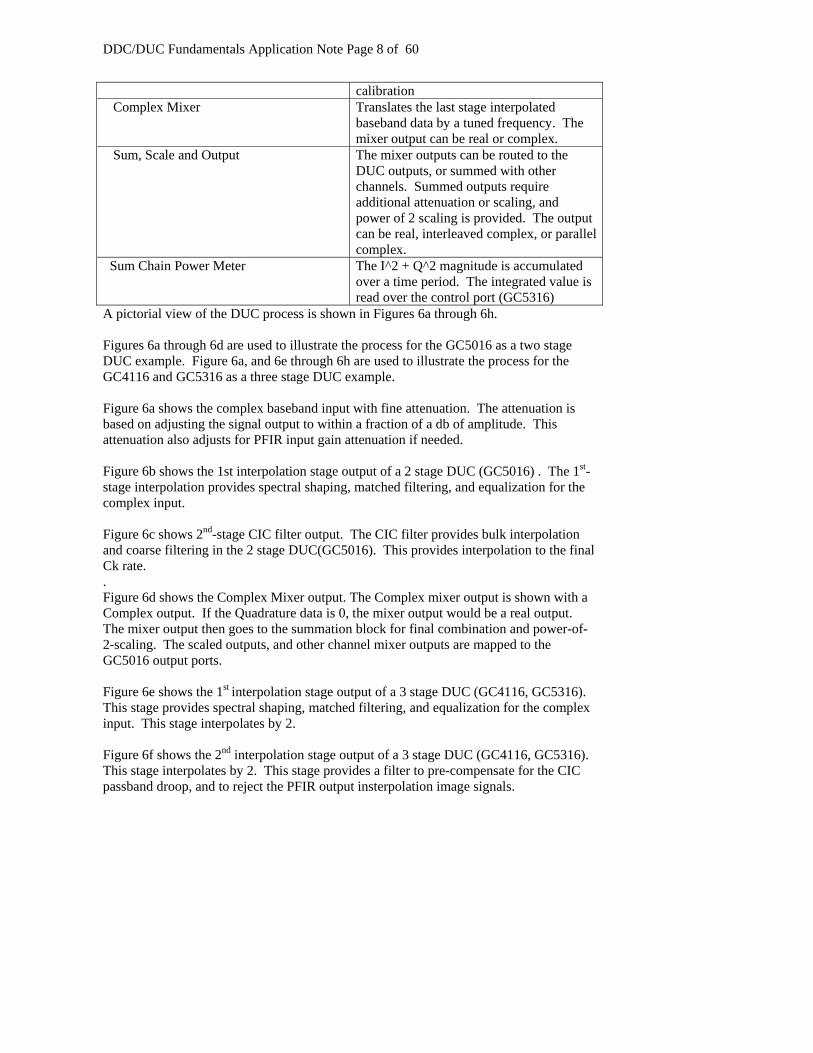
calibration Complex Mixer Translates the last stage interpolated
baseband data by a tuned frequency. The mixer output can be real or complex.
Sum, Scale and Output The mixer outputs can be routed to the DUC outputs, or summed with other channels. Summed outputs require additional attenuation or scaling, and power of 2 scaling is provided. The output can be real, interleaved complex, or parallel complex.
Sum Chain Power Meter The I^2 + Q^2 magnitude is accumulated over a time period. The integrated value is read over the control port (GC5316)
A pictorial view of the DUC process is shown in Figures 6a through 6h. Figures 6a through 6d are used to illustrate the process for the GC5016 as a two stage DUC example. Figure 6a, and 6e through 6h are used to illustrate the process for the GC4116 and GC5316 as a three stage DUC example. Figure 6a shows the complex baseband input with fine attenuation. The attenuation is based on adjusting the signal output to within a fraction of a db of amplitude. This attenuation also adjusts for PFIR input gain attenuation if needed. Figure 6b shows the 1st interpolation stage output of a 2 stage DUC (GC5016) . The 1st-stage interpolation provides spectral shaping, matched filtering, and equalization for the complex input. Figure 6c shows 2nd-stage CIC filter output. The CIC filter provides bulk interpolation and coarse filtering in the 2 stage DUC(GC5016). This provides interpolation to the final Ck rate. . Figure 6d shows the Complex Mixer output. The Complex mixer output is shown with a Complex output. If the Quadrature data is 0, the mixer output would be a real output. The mixer output then goes to the summation block for final combination and power-of-2-scaling. The scaled outputs, and other channel mixer outputs are mapped to the GC5016 output ports. Figure 6e shows the 1st interpolation stage output of a 3 stage DUC (GC4116, GC5316). This stage provides spectral shaping, matched filtering, and equalization for the complex input. This stage interpolates by 2. Figure 6f shows the 2nd interpolation stage output of a 3 stage DUC (GC4116, GC5316). This stage interpolates by 2. This stage provides a filter to pre-compensate for the CIC passband droop, and to reject the PFIR output insterpolation image signals.
DDC/DUC Fundamentals Application Note Page 9 of 60
Figure 6g shows 3rd-stage CIC filter output. The CIC filter provides bulk interpolation and coarse filtering in the 3 stage DUC(GC4116, GC5316). This provides interpolation to the final Ck rate. Note: In the GC5316, if the CDMA mode is used, the Mixer operates at ½ the Ck rate. Figure 6h shows the Complex Mixer output. The Complex mixer output is shown with a Complex output. If the Quadrature data is 0, the mixer output would be a real output. The mixer output then goes to the summation block for final combination and power-of-2-scaling. The scaled outputs, and other channel mixer outputs are mapped to the GC5316 output ports. The GC4116 has a single output port. 1.3 System Metrics The DDC/DUCs are part of an IF to baseband radio subsystem. The metrics used for the radio subsystem are not usually isolated between the antenna, RF to IF, IF to Baseband, and the baseband interface. These concepts are described below related to receiver sensitivity and transmit power quality. Receiver sensitivity – DDC – The signal of interest is input at a reduced level to the basestation antenna. Other interfering signals are added to the signal. The data output from the baseband modem is evaluated for Bit Error Rate (BER) The digital baseband modem has processing gain, spreading gain, and coding diversity to aid in the decoding of signals. The Signal to Noise Ratio (SNR) is also used as a reference to determine the sensitivity of the receiver. The DDC SNR can be affected by decimating filter stopband rejection, mixer spurious components, and AGC noise. Transmit power quality – DUC – The signal of interest and other frequencies are measured. Signal leakage is measured as a power ratio from the desired signal frequencies to the leakage signal frequencies as an Adjacent Channel Leakage Ratio (ACLR). The signal of interest is demodulated and checked for Composite Error Vector Magnitude (CEVM) and Peak Code Domain Error (PCDE). Modulation Error Rate (MER) and Error Vector Magnitude (EVM) - DUC - The MER is measured by receiving the analog transmit path after the digital baseband modem, DUC, and D/A converter. The received signal carrier is removed, the signal is match filtered, and the demodulator reports the deviation from the desired test-modulation data. The EVM is measured by receiving the analog transmit path after the D/A converter, translating to baseband, and recovering the IQ symbol data. The deviation from the desired IQ constellation point is determined for each symbol. The largest symbol error is reported as the EVM. Adjacent Channel Leakage Ratio (ACLR) – DUC – a measure of the leakage signal power to the main signal power as a log-ratio. There are defined band frequencies for the desired and leakage power measurements.
Comment [ah4]: Not sure what related to means.
DDC/DUC Fundamentals Application Note Page 10 of 60
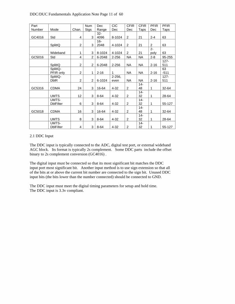
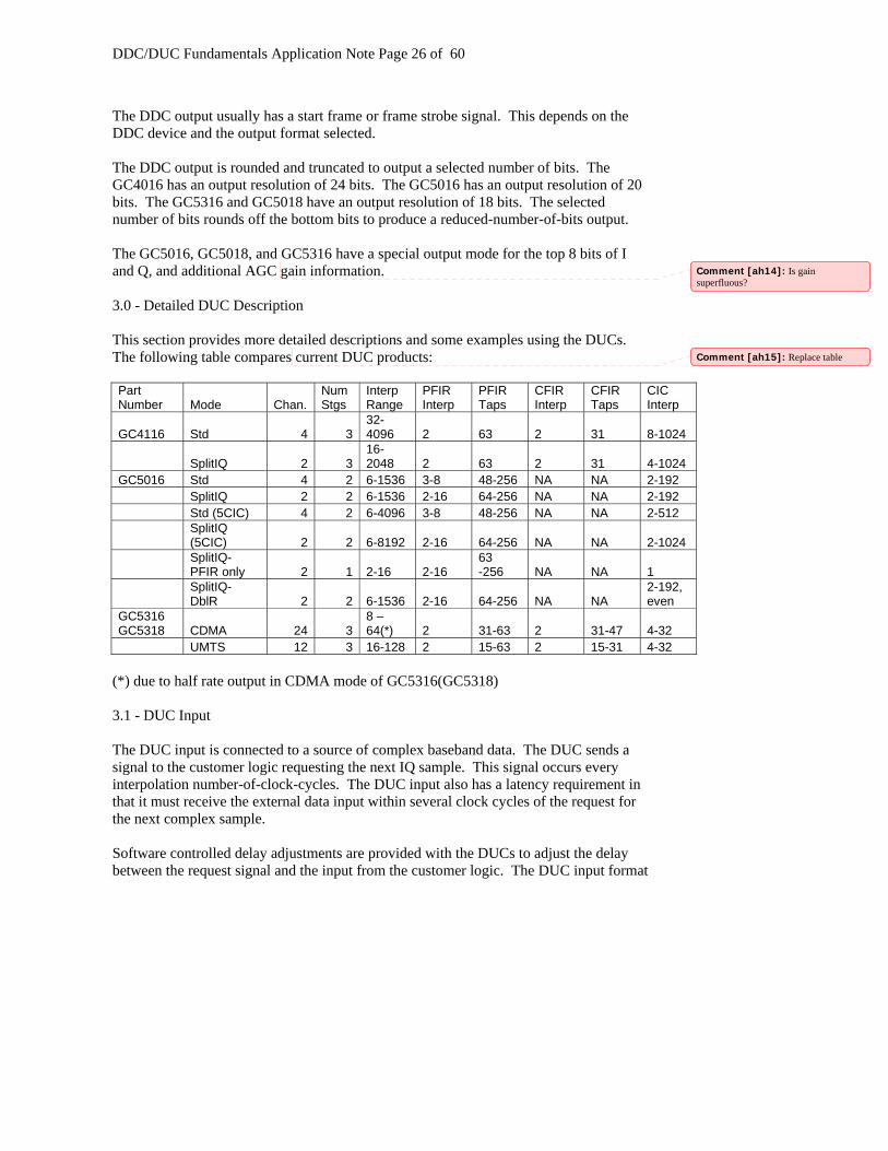
Spectral Mask – DUC – a measure of the leakage of undersired signals close to (near stopband) and further from the signal of interest (stopband). Most standards have a transmitter spectral mask as a power envelope. . 1.4 Spectral Mask The spectral mask is a visual guide to the channel frequency response. The channel response applies to both the DDC and DUC filter designs. An example of a spectral mask is shown in Figure 9. The spectral mask is divided into: Passband – The passband range is typically 0 to Fp,. In this section there is no attenuation over the passband range. The passband ripple is a combination of the stage filters convolved ripple over the passband range. It also includes CIC droop correction error. Transitionband – the transitionband is from Fp to Fs. This band may have an intermediate frequency and attenuation point. In the PFIR and CFIR design, this intermediate point is extended to a stopband requirement. Stopband – The stopband is from Fs to Fsample/2. In a two stage filter, the PFIR design and CIC stopband rejection provide the channel stopband rejection. In a three stage filter, a combination of the PFIR design, CFIR design, and CIC stopband rejection provides the channel stopband rejection. In most cases the PFIR filter defines the passband and transition band requirements. The CFIR filter provides CIC correction, transition band requirements, and 1st CIC image rejection. The CIC response, CFIR, and PFIR are combined to evaluate the effective channel response. There is more detail on this in Section 3.3. 2.0 Detailed DDC Description This section provides more detailed descriptions and some examples using the DDCs. The following table describes the current DDC products:
DDC/DUC Fundamentals Application Note Page 11 of 60
Part Number Mode Chan.
Num Stgs
Dec Range
CIC Dec
CFIR Dec
CFIR Taps
PFIR Dec
PFIR Taps
GC4016 Std 4 3 32-4096 8-1024 2 21 2-4 63
SplitIQ 2 3 16-2048 4-1024 2 21 2 63
Wideband 1 3 8-1024 4-1024 2 21 2-poly 63
GC5016 Std 4 2 6-2048 2-256 NA NA 2-8 95-255
SplitIQ 2 2 6-2048 2-256 NA NA 2-16 127-511
SplitIQ- PFIR only 2 1 2-16 1 NA NA 2-16
63 -511
SplitIQ- DblR 2 2 6-1024
2-256, even NA NA 2-16
127-511
GC5316 CDMA 24 3 16-64 4-32 2 14-48 1 32-64
UMTS 12 3 8-64 4-32 2 14-32 1 28-64
UMTS- DblFilter 6 3 8-64 4-32 2
14-32 1 55-127
GC5018 CDMA 16 3 16-64 4-32 2 14-48 1 32-64
UMTS 8 3 8-64 4-32 2 14-32 1 28-64
UMTS- DblFilter 4 3 8-64 4-32 2
14-32 1 55-127
2.1 DDC Input The DDC input is typically connected to the ADC, digital test port, or external wideband AGC block. Its format is typically 2s complement. Some DDC parts include the offset binary to 2s complement conversion (GC4016) . The digital input must be connected so that its most significant bit matches the DDC input port most significant bit. Another input method is to use sign extension so that all of the bits at or above the current bit number are connected to the sign bit. Unused DDC input bits (the bits lower than the number connected) should be connected to GND. The DDC input must meet the digital timing parameters for setup and hold time. The DDC input is 3.3v compliant.
DDC/DUC Fundamentals Application Note Page 12 of 60
DDC Input Type Number inputs Part number Real – 14bit 4 GC4016 Complex – 14bit 2 GC4016 Real – 16bit 3 GC4016 Real – 16bit 4 GC5016 Interleaved Complex – 16bit
4 GC5016
Complex – 16bit 2 GC5016 Double Rate Real – 16bit
2 GC5016
Double Rate Complex – 16bit
1 GC5016
Real – 16bit 4 GC5316 (umts mode)
Real – 16bit 2 GC5316 (cdma2000 mode) – using resampler
Real – 16bit 4 GC5316 (cdma2000 mode) – Rx clock 2x ADC clock
Complex – 16bit 2 GC5316 Real – 16bit 4 GC5018 Complex – 16bit 2 GC5018 Direct and bandpass ADC sampling – The RF / IF conversion, ADC sample rate, and DDC sample rate are used to determine the IF center frequency. ADC direct sampling provides a digitized IF output from the IF center frequency. ADC output in the bandpass or sub sampling mode provides an aliased sample rate. The digital IF output frequency is based on: Nyquist Zone 1 Digital IF frequency = IF frequency Nyquist Zone 2 Digital IF frequency = IF frequency – FsADC/2 Nyquist Zone 3 Digital IF frequency = - (IF frequency – FsADC) Nyquist Zone 4 Digital IF frequency = IF frequency – 3/2*FsADC Customer signal power and spectral inversion must be considered for direct and bandpass sampling.
DDC/DUC Fundamentals Application Note Page 13 of 60
Nyquist Zone
Sampling Method Frequency Range Spectra
1 Direct Sampling 0 to FsADC/2 Non-inverted 2 Sub Sampling FsADC/2 to FsADC Iinverted 3 Sub Sampling FsADC to 3*FsADC/2 Non-inverted 4 Sub Sampling 3*FsADC/2 to 2*FsADC Inverted Note: The tuning frequency can be positive or negative depending on the desired signal to be placed at baseband. The positive tuning frequency translates a negative signal frequency towards 0. The negative tuning frequency translates a positive frequency signal towards 0. Spectral inversion can be performed for complex signals through input port mapping (the GC5316 and GC4016 provide this feature through external connections and internal software; the GC5016 requires a specific I and Q order, so the external connections need to be compatible with the standard complex or reversed complexed order). Real and Complex Input – The DDC input can be real or complex. The common input modes are full-rate real and full-rate complex. The full rate complex mode requires two input ports. DDCs may require multiple channels to process full rate complex or double rate inputs. Zero Padding – If the ADC sample clock is a sub-multiple of the DDC input clock, the DDC input can insert 0-value samples to match the DDC input rate. Input signal power is lowered in this mode. Note: The ADC sample rate may be a sub-multiple (1/2, 1/3) of the DDC clock input. The DDC has programming to select one of multiple DDC inputs, GND, digital input channel, or diagnostic sources. 2.2 Complex Mixer The output of the DDC input block is input to the mixer block. The mixer provides complex frequency translation based on a Digital Local Oscillator (DLO) set for the tuning or down-conversion frequency. The tuning frequency is a negative frequency for down conversion. The input to the mixer for real only conditions has the input connected to the (I) in-phase signal. The (Q) quadrature input is zeroed. The mixer provides a sum and difference frequency translation Sum = Fin + Ftuning Difference = Fin – Ftuning The mixer multipliers are configured to: Iout = Iinput * cos(DLO Current Phase) – Qinput * sin(DLO Current Phase) Qout = Qinput * cos(DLO Current Phase) + Iinput * sin(DLO Current Phase)
DDC/DUC Fundamentals Application Note Page 14 of 60
The DLO current phase is developed from the integration of the programmed fractional phase (Ftune/Fclk), the initial and dither phases. The phase of the DLO is calculated using: Current Phase = Previous Phase + Tuning Word(Ftune/Fclk * Tuningword Resolution) + Initial Phase value + Phase Dither value There are special synchronization controls to allow multiple channels to start at the same time. These are used to lock multiple channels to a specific tuning frequency and initial phase. Phase dither is used to reduce the spur noise floor by spreading the noise energy across a larger bandwidth. In beam-forming, where multiple antennas are combined with a specific phase, the initial phase can be set as a bias value. The phase to sine() and phase to cosine() functions can generate spurious signals. The mixer SNR is better than 100db for the listed DDC devices. See Figure 7 for an example of frequency translation in the DDC mixer. 2.3 Filtering and Decimation The DDC input is sampled at an integer multiple of the DDC output rate. The filtering process provides a bandpass filter centered around the DLO frequency. The decimation process reduces the sample rate after the filtering action. At the DDC output, most demodulation processes, require two output complex samples per symbol. In some demodulators the DDC output has one complex sample per symbol. The I and Q data are low pass filtered with the same real coefficients. This provides the bandpass filter effect around the complex-baseband signal. The DDC processes of rejecting out of band frequencies and reducing the sample rate for the baseband demodulator are performed in one, two, or three filtering stages. The number of filtering stages is inversely proportional to the desired output bandwidth. Single Stage Decimating Filter
FIR GC5016 (2 channel)
Two Stage Decimating Filter
CIC, FIR GC5016 (4 channel)
Three Stage Decimating Filter
CIC, CFIR, PFIR GC5316 (24, 12, 6 channel)
Three Stage Decimating Filter
CIC, CFIR, PFIR GC5018 (16, 8, 4 channel)
Three Stage Decimating Filter
CIC, CFIR, PFIR (Resampler)
GC4016 (4, 2, 1 channel)
DDC/DUC Fundamentals Application Note Page 15 of 60
Note: The GC4016 Resampler takes the channel output from the PFIR, provides an NDELAY interpolation, and the output counter (RES_RATIO) determines when the output sample occurs. The polyphase index is estimated, and an NMULT tap filter based on the polyphase is applied to the PFIR data. The output sample is then stored for this channel. Figure 8a shows a typical channel response for a decimate by 4 single stage decimating filter. Figure 8b shows a typical channel response for a 2 stage decimating filter, where the CIC and PFIR filters decimate by 16. Figure 8c shows the GC5316 3 stage decimating filter where the CIC, CFIR, and PFIR filters decimate by 16. A single stage decimating filter design is used for decimations from 2 to 8. It is a PFIR filter. In the two stage decimating filter, the 1st stage CIC and 2nd-stage PFIR are combined. The two stage PFIR filter decimates by a ratio of 2 to 5. In the three stage decimating filter, The 1st stage is a CIC filter. The 2n- and 3r- stages FIR filters decimations depend on the device selected (GC5316 – 2,1), (GC4016 – 2,2). The two stage decimating filter design is used for decimations from 6 to 1024. The 1st-stage decimating filter is a Cascade Integrator Comb (CIC) filter. The 2nd -stage decimating filter is a PFIR filter. In the two stage decimating filter design, the ratio of decimations between the 1st - and 2nd-stage decimating filters is based on the desired stopband rejection. The power response of the CIC filter at the Ck/CIC decimation – PFIR passband determines the amount of CIC rejection. In the two stage decimating filter, the CIC M value is 1. The GC5016 CIC channel rejection estimate is further described in section 2.4, using a 5 stage CIC, and M = 1. As more of the CIC bandwidth is utilized the CIC Power response increases, which lowers the available channel stopband rejection. The 2nd-stage decimation is set for the lowest integer of 2, 3, 4, or 5, based on the clock oversampling rate and an integer CIC decimation. If the DDC output rate is 2 samples per symbol, the 2nd-stage decimation is normally set to 2 or 3. To compute the decimation factors: Fclk / Fsymbol = oversample factor If FDDCOut >= 2 * Fsymbol 2nd-stage decimation factor = 2, 3, 4, or 5 Else 2nd-stage decimation factor = 2, 3, 4, or 5 End 1st-stage decimation factor = (Oversample Factor / FDDCOut) / 2nd stage decimation factor
DDC/DUC Fundamentals Application Note Page 16 of 60
The three stage decimating filter design (GC5316/GC5018) is used for decimations from 8 to 64. The GC5316/GC5018 2ndstage decimating filter CFIR has a fixed decimation of 2. The GC5316/GC5018 3rd –stage decimating filter PFIR has a fixed decimation of 1. The three stage GC5316/GC5018 has a selectable M factor for the 6 stage CIC. The CIC rejection is improved over the 2 stage design, due to the addition of the CFIR 2nd stage FIR filter. The GC5316 CIC channel rejection estimate is further described in section 2.4. The three stage decimating filter design (GC4016) is used for decimations from 16 to 4096. The GC4016 2nd-stage decimating filter CFIR has a fixed decimation of 2. The GC4016 3rd-stage decimating filter PFIR has a fixed decimation of 2. The GC4016 has a resampler filter following the PFIR filter. The GC4016 5 stage CIC channel rejection estimate is further described in section 2.4. Note: A special mode of the GC4016, called Wideband down convert mode, polyphases two pairs of DDC channels to make a single channel. In this case the cic_decimation is ½ the programmed value. Multistage Decimation Examples The output IQ rate (Fsymbol) for IS95, IS136, CDMA2000, UMTS requires 2 samples per symbol. The output IQ rate for other systems may be 1 sample per symbol. Example – Input 16x WCDMA, Output 2x WCDMA Two stage (GC5016) DDC - CIC and PFIR filter CIC decimation – 4 CIC output rate- 4x PFIR decimation – 2 PFIR output rate – 2x Example – Input 16x WCDMA, Output 2x WCDMA Three stage (GC5316) DDC – CIC, CFIR, and PFIR filter CIC decimation – 4 CIC output rate- 4x CFIR decimation – 2 CFIR output rate – 2x PFIR decimation – 1 PFIR output rate – 2x Example – Input 100x CDMA2000, Output 2x Two Stage DDC – CIC, and PFIR filter CIC decimation – 25, CIC input rate 100x CIC output rate -4x PFIR decimation 2, PFIR input rate- 4x PFIR output rate – 2x
DDC/DUC Fundamentals Application Note Page 17 of 60
Example – Input 100x CDMA2000, Output 2x Three Stage (GC5316) DDC – CIC, CFIR, and PFIR filter Input ADC rate is 50x Mixer operates on ½ rate channels Zpad of 2 to IQ mixer output of 100x CIC decimation – 25, CIC input rate 100x
CIC output rate 4x CFIR decimation 2, CFIR input rate 4x CFIR output rate – 2x PFIR decimation 1, PFIR input rate 2x PFIR output rate – 2x
Example – Input 64x CDMA2000, Output 2x Three Stage (GC4016) DDC – CIC, CFIR, and PFIR filter CIC decimation – 8, CIC input rate 72x CIC output rate 8x CFIR decimation 2, CFIR input rate 8x CFIR output rate – 4x PFIR decimation 2, PFIR input rate 4x PFIR output rate – 2x In a (GC5016 splitIQ) single stage decimating filter, the channel response is the PFIR designed response. In a (GC5016) two stage decimating filter, the 1st-stage filter is a CIC filter that provides bulk decimation. The 2nd-stage decimating PFIR filter is designed as a pulse shaping or low pass filter combined with the CIC correction filter coefficients. The CIC and PFIR filters are combined for the channel response. In a (GC4016, GC5316, GC5018) three stage decimating filter, the 1st-stage filter is a CIC filter that provides bulk decimation. The 2nd-stage CFIR filter is designed as a low pass filter combined with the CIC correction filter coefficients. The 3rd stage PFIR filter is designed as a low pass or pulse shaping filter. The CIC, CFIR, and PFIR filters are combined for the channel response. 2.4 CIC Filter – 1st Decimating Filter in Multistage Decimation DDC The CIC filter provides an approximation of a boxcar filter. The CIC response depends on the number of stages and number of delays (M) in each integrator stage. There are several important parameters in using the CIC filter. The passband droop in the CIC over the desired bandwidth requires compensation in the next stage filter. See Figure 10 for the CIC response. The CIC Response is estimated as:
Comment [ah5]: Go over all of this to check on hyphen or minus signs
DDC/DUC Fundamentals Application Note Page 18 of 60
P(f) = ( sin (pi * M * f) / sin ( pi * f / R) ) ^ (2 * N) [Reference 5] Where (f) is the CIC output frequency (Ckin / cic_decimation). (M) is the CIC Delay, 1 for GC4016, and GC5016, programmable 1,2 for GC5316 (R) is the rate change through the CIC filter, cic_decimation (N) is the number of CIC stages, 5 for GC4016 and GC5016, 6 for GC5316 The CIC filter can have five or six stages. As the number of stages increases, the stopband attenuation increases, and more droop correction is required. The CIC filter droop correction affects the channel-filter passband flatness. The channel passband is limited by the desired stopband rejection [Table 2 Reference 5]. The GC4016 and GC5016 CIC filter has an M of 1. The GC5316 and GC5018 have a sharpened CIC filters where the M value can be 1 or 2. This effectively increases the box car number of taps in each stage from decimation ratio to decimation ratio * M. DDC Part Number Number CIC stages M value GC4016 5 1 GC5016 5 1 GC5316 6 1, 2 GC5018 6 1, 2 See Figure 11 for an example of a channel response, where the CIC stage decimates by 4. The CIC stage has gain correction to compensate for the CIC integrator added gain. The gain equation provides the 1/ (NumCICstages ^ (CIC Decimation * Mvalue)) shift value for the integrator. The GC5016, GC5316, and GC5018 have additional CIC output gain shift values that must also be calculated. The GC5016 CIC filter output has additional requirements to limit the Input magnitude to ½ the normalized value if symmetric filters are utilized in the PFIR hardware. 2.5 CIC Filter Droop Correction The CIC filter determines which droop correction high pass filter is utilized. The CIC droop correction is normally a 3 tap filter, which is convolved with the 2nd-stage decimating filter. The suggested CIC correction array can be modified to minimize passband error. CIC stage M value CIC comp
taps 5 1 [-.15, 1, -.15] 6 1 [-.17, 1, -.17] 6 2 [-.32, 1, -.32]
DDC/DUC Fundamentals Application Note Page 19 of 60
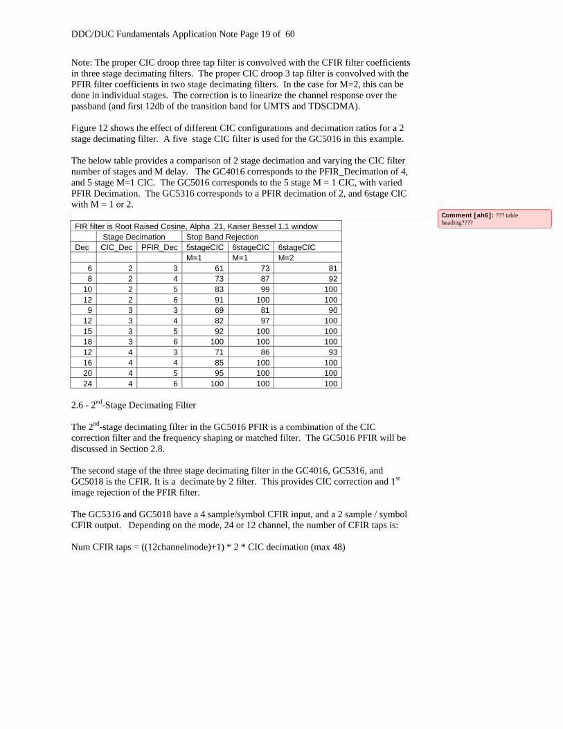
Note: The proper CIC droop three tap filter is convolved with the CFIR filter coefficients in three stage decimating filters. The proper CIC droop 3 tap filter is convolved with the PFIR filter coefficients in two stage decimating filters. In the case for M=2, this can be done in individual stages. The correction is to linearize the channel response over the passband (and first 12db of the transition band for UMTS and TDSCDMA). Figure 12 shows the effect of different CIC configurations and decimation ratios for a 2 stage decimating filter. A five stage CIC filter is used for the GC5016 in this example. The below table provides a comparison of 2 stage decimation and varying the CIC filter number of stages and M delay. The GC4016 corresponds to the PFIR_Decimation of 4, and 5 stage M=1 CIC. The GC5016 corresponds to the 5 stage M = 1 CIC, with varied PFIR Decimation. The GC5316 corresponds to a PFIR decimation of 2, and 6stage CIC with M = 1 or 2. FIR filter is Root Raised Cosine, Alpha .21, Kaiser Bessel 1.1 window Stage Decimation Stop Band Rejection Dec CIC_Dec PFIR_Dec 5stageCIC 6stageCIC 6stageCIC M=1 M=1 M=2
6 2 3 61 73 818 2 4 73 87 92
10 2 5 83 99 10012 2 6 91 100 100
9 3 3 69 81 9012 3 4 82 97 10015 3 5 92 100 10018 3 6 100 100 10012 4 3 71 86 9316 4 4 85 100 10020 4 5 95 100 10024 4 6 100 100 100
2.6 - 2nd-Stage Decimating Filter The 2nd-stage decimating filter in the GC5016 PFIR is a combination of the CIC correction filter and the frequency shaping or matched filter. The GC5016 PFIR will be discussed in Section 2.8. The second stage of the three stage decimating filter in the GC4016, GC5316, and GC5018 is the CFIR. It is a decimate by 2 filter. This provides CIC correction and 1st image rejection of the PFIR filter. The GC5316 and GC5018 have a 4 sample/symbol CFIR input, and a 2 sample / symbol CFIR output. Depending on the mode, 24 or 12 channel, the number of CFIR taps is: Num CFIR taps = ((12channelmode)+1) * 2 * CIC decimation (max 48)
Comment [ah6]: ??? table heading????
DDC/DUC Fundamentals Application Note Page 20 of 60
The CFIR filter design is based on rejecting the PFIR image. The CFIR input rate is 4 samples / symbol. The stopband for the decimate by 2 filter to meet the Nyquist requirement is 1 sample/symbol. The passband Fs is typically adjusted to meet the ½ sample / symbol requirement. Due to the need to convolve the CIC correction, 2 taps are removed from the total. An example of a 46 tap CFIR filter is shown in Figure 11. An example of CFIR filter design is: 48 tap CFIR, 46 taps for low pass filter, 2 taps for CIC correction – 1 tap CFIR input, 4 samples/symbol – 4.9152Mhz (FIR sample clock) Fp - .65Mhz Fs - 1.2288Mhz(Nyquist), (alternate method –2.4576 – (Fp * 1.25) ) Desired stopband rejection – 85dbc 18bit fixed point coefficients Figure 12 shows the image rejection of the GC5316 PFIR and CFIR combined, to develop an 85dbc r stopband rejection. The GC4016 CFIR design is based on 21taps and 8 samples per symbol. The CFIR coefficients are 16bit resolution. The GC4016 uses a five stage CIC M=1 one stage correction filter. Due to the need to convolve the CIC correction, 2 taps are removed from the total, the CFIR has 19 taps for design. The GC4016 CFIR is designed with a wide transitionband (past the filter Nyquist frequency), to provide stopband attenuation of the PFIR decimation image response. An equivalent CFIR is shown for a 64x input, where the CIC decimates by 8, the CFIR decimates by 2, and the PFIR decimates by 2. The GC4016 output is 2 samples/symbol. Figure 13 shows an example of a CFIR filter designed for the GC4016. CFIR Input 8 samples/symbol – 9.8304Mhz (FIR sample clock) Fp .65 Fs – 2.4576 (past Nyquist is 4.9152 – (1.25 * Fp) ) Desired stopband rejection – 85dbc 16bit fixed point coefficients Figure 14 shows the CFIR and PFIR response for the GC4016. 2.7 - 3rd-stage Decimation Filter (PFIR) A 3rd-stage decimation filter is used in the GC5018, GC5316 and GC4016. The GC5018 and GC5316 can combine PFIR filtering in 2 channels to increase the number of PFIR filter taps. The GC4016 has a fixed 63 tap PFIR. The PFIR can be decimate by 2 or 4.
DDC/DUC Fundamentals Application Note Page 21 of 60
The GC5018 and GC5316 filter decimates by 1 (i.e. no decimation). If the GC5018 and GC5316 output is 2 samples / symbol, the standard filter design is performed with a 2x sample clock. If the GC5316 or GC5018 output is 1 sample / symbol, for TDSCDMA, the PFIR is still designed with a 2x sample clock, decimate by 2 filter, and the output block or external logic performs the decimation after the PFIR. GC5316 DDC channels PFIR equation Max PFIR taps 24 2 * Input rate / Output rate 64 12 4 * Input rate / Output rate 64 6 8 * Input rate / Output rate 127 GC5018 DDC channels PFIR equation Max PFIR taps 16 2 * Input rate / Output rate 64 8 4 * Input rate / Output rate 64 4 8 * Input rate / Output rate 127 Figure 15 shows the GC5316/GC5018 64 tap PFIR, used with the above CFIR section on the 2nd- stage decimating filter. The GC5316/GC5018 PFIR design requirements are: PFIR input - 2 samples/symbol PFIR taps – 64 PFIR Fp - .6 PFIR Fs - .7 Desired stopband rejection - 85 dbc 18bit fixed point coefficients The GC4016 PFIR has a fixed 63 taps and decimates by 2. Figure 16 shows the 63 tap PFIR, used with the above CFIR section on the 2nd-stage decimating filter. The GC4016 PFIR requirements are: PFIR input - 4 samples/symbol PFIR taps – 63 PFIR Fp - .6 PFIR Fs - .72 Desired stopband rejection - 70 dbc 16bit fixed point coefficients 2.8 - GC5016 PFIR – 2nd-stage, two stage decimating filter The GC5016 PFIR is the 2nd-stage decimating filter. The number of filter taps depends on the number of channels used, the cic_dec, the pfir_dec, and filter symmetry. The PFIR has implementation limitations if the cic or pfir decimation is an odd number. There are additional limitations of 8 IQ samples in 4 channel mode, or 16 for split IQ modes. The cmd5016 programming tool is used to determine the number of taps. The ‘.ANL’ file lists the PFIR number of tap options when configuring the PFIR for the GC5016.
DDC/DUC Fundamentals Application Note Page 22 of 60
The GC5016 in 4 channel DDC mode performs I and Q filtering in the same channel. The GC5016 in splitIQ mode (2 channel) performs I and Q filtering with separate channels. In the 4 channel mode: numPFIR taps = 2 * 16 * fir_dec * int( min(cic_dec, 16/fir_dec)/2) – 1 (max 255) In the 2 channel split IQ mode: numPFIR taps = 2 * 16 * fir_dec * int( min(cic_dec, 16/fir_dec) ) – 1 (max 511) 2 taps are subtracted from the numPFIR taps to allow for the CIC Correction, in the 2 stage design. In the single stage design this is not needed, and all of the numPFIR taps can be used. The GC5016 can utilize symmetric taps or non symmetric taps. The tap file input to cmd5016 is analyzed for even, odd, or no symmetry. Odd symmetry results in more usable taps. The GC5016 PFIR coefficients have 16bit resolution. 2.9 - FIR Filter Design in DDCs FIR filter design is usually based on the receive signal standard implemented for the PFIR. The CFIR (as described above) is designed as a low pass filter with CIC correction taps. The two main FIR design types are: Low Pass – passband, transition band, and stopband frequency and amplitudes are entered to match a spectral mask Raised Cosine – matched filter design, a desired shape, (cosine or raised cosine) and oversampling factor are used to reduce Inter-Symbol Interference by shaping the transition and stopband nulls in the signal to be multiples of the symbol period. Low Pass Filter Design. The Parks McClellan, equal-ripple, or least squares methods generate filter based on input requirements. Using the passband, transition-band, stopband, and PFIR input rate, the user can specify the input to the filter design. The number of taps of the PFIR must be estimated before beginning the design. In some DDCs, the number of taps is fixed. In others, the number of taps is based on the processing time period (number-of-clocks) and the number of adder / multipliers. The filter passband is from DC to the edge of the passband (Fp). The transition band is from Fp to the edge of the stopband (Fs). The stopband is from Fs to Fclk_PFIR/2.
Comment [ah7]: Very weird sentence
Comment [ah8]: Not clear what this list is
DDC/DUC Fundamentals Application Note Page 23 of 60
The number of taps estimate (Parks McClellan) is based on computing the normalized transition bandwidth, and using the equation: b = (Fs – Fp) / PFIR clock numtaps = 2/3 * log10( 1/ (10 * (10^(Passbandripple_db/20)-1) * (10^(stopbandrej/20))/b [Reference 6] Fp – highest passband frequency Fs – lowest stopband frequency PFIR clock – PFIR (or CFIR) input clock rate Passband ripple_db – desired ripple usually < .2dbc Stopband rejection_db – desired minimum stopband rejection – usually > 65dbc The CFIR passband is either the PFIR passband + 5% for Low pass systems, or the PFIR passband + the first 12db of the transition band for pulse shaping systems. The CFIR stopband frequency depends on the desired PFIR image suppression, and the number of taps. In the GC4016 this is limited to 21 taps, 19 for the filter design, and 3 for the CIC correction. Typically the PFIR filter is interpolated by 2, and the desired attenuation value is determined in the image spectrum, as the Fs for the CFIR. In the GC5018 and GC5316, the CFIR design may reserve more than 3 taps for CIC correction, if the CIC M=2 is used. 3 to 7 CIC correction taps have been used, depending on the desired passband matching needed. The PFIR design method uses the spectrum mask to define the most limiting stopband frequency and the highest passband frequency. If the spectrum mask has multiple slopes and plateaus, a most limiting slope is used in the filter design. If windowing is used to reduce the passband ripple and stopband rejection (ripple) the passband needs to be extended, and the stopband frequency Fs is reduced. As the windowing operation lowers the transition band slope. Different windowing methods apply different slope factors. One example is to design filter coefficients with the Parks McClellan algorithm: PFIR input rate CDMA2000 2x, PFIR output rate CDMA2000 2x PFIR clock rate: 2.4576e6 Passband ripple .1db Stopband rejection 85db Fp = .61e6 Fs = .745e6 The estimate for this filter is 63 taps. Another example is to design filter coefficients with the Parks McClellan algorithm: PFIR input rate CDMA2000 4x, PFIR output rate CDMA2000 2x PFIR clock rate: 4.9152e6 Passband ripple .1db
Comment [ah9]: Do we want colons throughout?
DDC/DUC Fundamentals Application Note Page 24 of 60
Stopband rejection 85db Fp = .61e6 Fs = .745e6 The estimate for this filter is 126 taps. Windowing can be used to reduce the passband and stopband ripples. Windowing reduces Fp and increases Fs, effectively raising the normalized transition bandwidth. A standard windowing method is to use a Kaiser Bessel window with a Beta of .1. Root Raised or Raised Cosine Filter (Matched Filter) Design A raised cosine filter or root raised cosine filter has special tap values that develop a null amplitude at multiples of the symbol rate. 2 or 4 times the symbol rate is the FIR filter clock rate. The Alpha excess bandwidth parameter is specified in the receive standard. The PFIR RRC filter is normally designed to span from 16 to 64 symbols. The PFIR decimation value and the symbol span determine the filter tap size. The Alpha value for IS136 is .25. The Alpha value in UMTS, WCDMA, and TDSCDMA is .22. Windowing can be used to increase the stopband attenuation. Since this extends the transitionband, the Alpha excess bandwidth is reduced. Typical values for UMTS / WCDMA are .215 alpha, and Kaiser Bessel Beta of 1.1. If the PFIR filter spans more than 32 symbols, a hybrid filter can be generated that has both root raised cosine and low pass sections. The hybrid filter can be used in both the two stage and the three stage decimating filters. 2.10 - DDC Gain Adjustment and AGC PFIR output is decimated to 1 or 2 samples per symbol. The desired channel bandwidth has been filtered, but the output IQ amplitude may not be optimal for the baseband receiver input. The GC5016, GC5018, and GC5316 have narrowband AGC that can adjust the IQ amplitude to an average threshold. All of the DDCs have narrowband gain adjustments which can be set manually to multiply the fractional gain by the IQ data at the PFIR output. Reference [1, 2, 3, and 7] discuss DDC gain settings. Reference [8] discusses the Narrowband AGC settings and optimization for the GC5016. The manual gain is adjusted to make up for gain losses in the previous stages, and to adjust the AGC = 1.0 Av gain value.
Comment [ah10]: ?
Comment [ah11]: Odd sentence
DDC/DUC Fundamentals Application Note Page 25 of 60
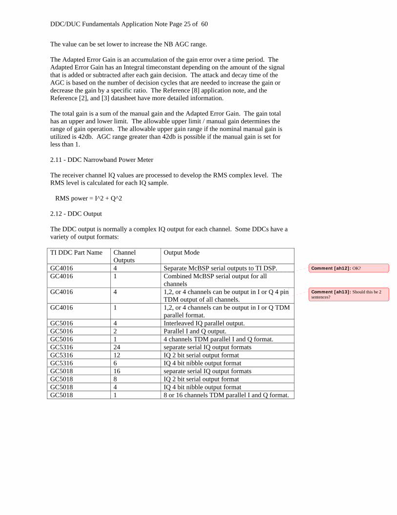
The value can be set lower to increase the NB AGC range. The Adapted Error Gain is an accumulation of the gain error over a time period. The Adapted Error Gain has an Integral timeconstant depending on the amount of the signal that is added or subtracted after each gain decision. The attack and decay time of the AGC is based on the number of decision cycles that are needed to increase the gain or decrease the gain by a specific ratio. The Reference [8] application note, and the Reference [2], and [3] datasheet have more detailed information. The total gain is a sum of the manual gain and the Adapted Error Gain. The gain total has an upper and lower limit. The allowable upper limit / manual gain determines the range of gain operation. The allowable upper gain range if the nominal manual gain is utilized is 42db. AGC range greater than 42db is possible if the manual gain is set for less than 1. 2.11 - DDC Narrowband Power Meter The receiver channel IQ values are processed to develop the RMS complex level. The RMS level is calculated for each IQ sample. RMS power = I^2 + Q^2 2.12 - DDC Output The DDC output is normally a complex IQ output for each channel. Some DDCs have a variety of output formats: TI DDC Part Name Channel
Outputs Output Mode
GC4016 4 Separate McBSP serial outputs to TI DSP. GC4016 1 Combined McBSP serial output for all
channels GC4016 4 1,2, or 4 channels can be output in I or Q 4 pin
TDM output of all channels. GC4016 1 1,2, or 4 channels can be output in I or Q TDM
parallel format. GC5016 4 Interleaved IQ parallel output. GC5016 2 Parallel I and Q output. GC5016 1 4 channels TDM parallel I and Q format. GC5316 24 separate serial IQ output formats GC5316 12 IQ 2 bit serial output format GC5316 6 IQ 4 bit nibble output format GC5018 16 separate serial IQ output formats GC5018 8 IQ 2 bit serial output format GC5018 4 IQ 4 bit nibble output format GC5018 1 8 or 16 channels TDM parallel I and Q format.
Comment [ah12]: OK?
Comment [ah13]: Should this be 2 sentences?
DDC/DUC Fundamentals Application Note Page 26 of 60
The DDC output usually has a start frame or frame strobe signal. This depends on the DDC device and the output format selected. The DDC output is rounded and truncated to output a selected number of bits. The GC4016 has an output resolution of 24 bits. The GC5016 has an output resolution of 20 bits. The GC5316 and GC5018 have an output resolution of 18 bits. The selected number of bits rounds off the bottom bits to produce a reduced-number-of-bits output. The GC5016, GC5018, and GC5316 have a special output mode for the top 8 bits of I and Q, and additional AGC gain information. 3.0 - Detailed DUC Description This section provides more detailed descriptions and some examples using the DUCs. The following table compares current DUC products: Part Number Mode Chan.
Num Stgs
Interp Range
PFIR Interp
PFIR Taps
CFIR Interp
CFIR Taps
CIC Interp
GC4116 Std 4 3 32-4096 2 63 2 31 8-1024
SplitIQ 2 3 16-2048 2 63 2 31 4-1024
GC5016 Std 4 2 6-1536 3-8 48-256 NA NA 2-192 SplitIQ 2 2 6-1536 2-16 64-256 NA NA 2-192 Std (5CIC) 4 2 6-4096 3-8 48-256 NA NA 2-512
SplitIQ (5CIC) 2 2 6-8192 2-16 64-256 NA NA 2-1024
SplitIQ- PFIR only 2 1 2-16 2-16
63 -256 NA NA 1
SplitIQ- DblR 2 2 6-1536 2-16 64-256 NA NA
2-192, even
GC5316 GC5318 CDMA 24 3
8 – 64(*) 2 31-63 2 31-47 4-32
UMTS 12 3 16-128 2 15-63 2 15-31 4-32 (*) due to half rate output in CDMA mode of GC5316(GC5318) 3.1 - DUC Input The DUC input is connected to a source of complex baseband data. The DUC sends a signal to the customer logic requesting the next IQ sample. This signal occurs every interpolation number-of-clock-cycles. The DUC input also has a latency requirement in that it must receive the external data input within several clock cycles of the request for the next complex sample. Software controlled delay adjustments are provided with the DUCs to adjust the delay between the request signal and the input from the customer logic. The DUC input format
Comment [ah14]: Is gain superfluous?
Comment [ah15]: Replace table
DDC/DUC Fundamentals Application Note Page 27 of 60
is 2s complement. The delay implementation method is different between the DUC devices. DUC inputs can have up to 16 bits of resolution. Unused inputs are usually zeroed. Some QAM type inputs need a bias value of ½. This changes the highest unused bit to a ‘1’. DUC input must meet the timing parameters for setup and hold time. The DUC input is 3.3v compliant. DUC Input Type Number inputs Part number Complex – 32bit serial 4 GC4116 Complex – 16bit I and Q serial 2 GC4116 Complex – 8bit parallel I and Q 4 GC5016 Complex – 16bit interleaved I and Q 4 GC5016 Complex – 16bit parallel I and Q 2 GC5016 Complex - TDM interleaved IQ and channel data 1 GC5016 Complex – 36bit serial 24 GC5316/GC5318 Complex, I and Q 18bit serial data 12 GC5316/GC5318 All of the DUCs have software programmed user channel clocks. These clocks are output to the customer logic with the Next IQ or Frame Strobe information to synchronize the transmission of the next IQ data. The DUC input must receive the next IQ data at the proper time, or an IQ sample will be repeated. The DUC divided clock must allow the number of IQ bits to be received within each interpolation number of Ck clocks. The GC4116 has a uprocessor bus register for manual IQ updates that can be used to input an I and Q constant value, or for low-modulation rate signals. The GC4116 serial input can be connected to a TI-McBSP DSP output. The serial packet timing needs to be deterministic to maintain the IQ input at the symbol rate. Note: Special diagnostic controls are provided in the GC4116 and GC5016 to provide a DC and GND value for initial CW tone testing, without the customer logic input being driven. 3.2 - DUC Input Gain The DUC channel typically has a fine gain control before the PFIR input. The fine gain is used to adjust the IQ amplitude to prevent clipping and to adjust for fractional gain losses in the DUC channel. References [2,3,4, and 9] discuss the DUC Gain adjustment procedures. The GC5016 fine gain is adjusted through the use of the overall_gain parameter or as a manual parameter.
Comment [ah16]: Check exact meaning
Comment [ah17]: Too many tos.
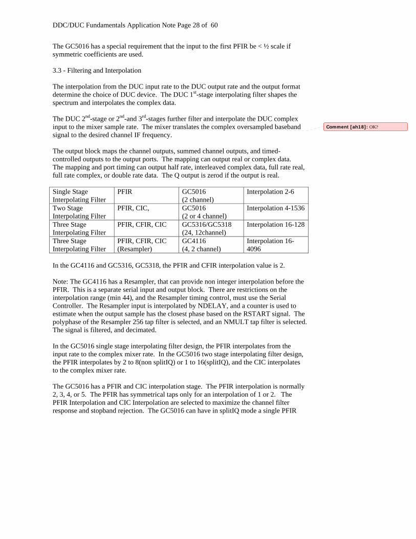
DDC/DUC Fundamentals Application Note Page 28 of 60
The GC5016 has a special requirement that the input to the first PFIR be < ½ scale if symmetric coefficients are used. 3.3 - Filtering and Interpolation The interpolation from the DUC input rate to the DUC output rate and the output format determine the choice of DUC device. The DUC 1st-stage interpolating filter shapes the spectrum and interpolates the complex data. The DUC 2nd-stage or 2nd-and 3rd-stages further filter and interpolate the DUC complex input to the mixer sample rate. The mixer translates the complex oversampled baseband signal to the desired channel IF frequency. The output block maps the channel outputs, summed channel outputs, and timed-controlled outputs to the output ports. The mapping can output real or complex data. The mapping and port timing can output half rate, interleaved complex data, full rate real, full rate complex, or double rate data. The Q output is zerod if the output is real. Single Stage Interpolating Filter
PFIR GC5016 (2 channel)
Interpolation 2-6
Two Stage Interpolating Filter
PFIR, CIC, GC5016 (2 or 4 channel)
Interpolation 4-1536
Three Stage Interpolating Filter
PFIR, CFIR, CIC GC5316/GC5318 (24, 12channel)
Interpolation 16-128
Three Stage Interpolating Filter
PFIR, CFIR, CIC (Resampler)
GC4116 (4, 2 channel)
Interpolation 16-4096
In the GC4116 and GC5316, GC5318, the PFIR and CFIR interpolation value is 2. Note: The GC4116 has a Resampler, that can provide non integer interpolation before the PFIR. This is a separate serial input and output block. There are restrictions on the interpolation range (min 44), and the Resampler timing control, must use the Serial Controller. The Resampler input is interpolated by NDELAY, and a counter is used to estimate when the output sample has the closest phase based on the RSTART signal. The polyphase of the Resampler 256 tap filter is selected, and an NMULT tap filter is selected. The signal is filtered, and decimated. In the GC5016 single stage interpolating filter design, the PFIR interpolates from the input rate to the complex mixer rate. In the GC5016 two stage interpolating filter design, the PFIR interpolates by 2 to 8(non splitIQ) or 1 to 16(splitIQ), and the CIC interpolates to the complex mixer rate. The GC5016 has a PFIR and CIC interpolation stage. The PFIR interpolation is normally 2, 3, 4, or 5. The PFIR has symmetrical taps only for an interpolation of 1 or 2. The PFIR Interpolation and CIC Interpolation are selected to maximize the channel filter response and stopband rejection. The GC5016 can have in splitIQ mode a single PFIR
Comment [ah18]: OK?
DDC/DUC Fundamentals Application Note Page 29 of 60
interpolation stage with the CIC interpolation of 1. See Figure 19a for an example of a single stage interpolating filter response. The GC5016 two stage CIC filter interpolation is calculated as: CIC Interpolation = ( Ckrate / DUC Inputrate) / PFIR Interpolation. Windowing the PFIR coefficients may increase the PFIR stopband rejection. See Figure 19b for an example of a two stage interpolating filter response. The three stage GC4116 and GC5316 have a PFIR, CFIR, and a CIC interpolation stage. The PFIR and CFIR have an interpolation of 2. The CIC filter interpolation for the 3 stage interpolation is calculated as: CIC Interpolation = ( Tx_rate / DUC Inputrate) / 4. See Figure 19c for an example of a GC5316/GC5318 three stage interpolating filter response. Multistage Interpolation Examples The output IQ rate for IS95, IS136, CDMA2000, and UMTS requires 2 samples per symbol. The output IQ rate for other systems may be 1 sample per symbol. Example – Input 1x WCDMA, output 16x WCDMA real or parallel complex Output 8x WCDMA interleaved complex Two stage (GC5016) DUC - PFIR and CIC filter PFIR interpolation – 4 PFIR output rate – 4x CIC interpolation – 4 CIC output rate 16x Channel summation Interleaved complex output – decimates by 2 to select I or Q Example – Input 1x WCDMA, output 16x WCDMA real or parallel complex Output 8x WCDMA interleaved complex Three stage (GC5316) DDC – CIC, CFIR, and PFIR filter PFIR interpolation – 2 PFIR output rate – 2x CFIR interpolation – 2 CFIR output rate – 4x CIC interpolation – 4 CIC output rate -16x Channel summation Interleaved complex output – decimates by 2 to select I or Q
DDC/DUC Fundamentals Application Note Page 30 of 60
Example – Input 1x CDMA2000, output 50x interleaved IQ Three stage (5316) DDC – CIC, CFIR, and PFIR filter PFIR interpolation – 2 PFIR output rate – 2x CFIR interpolation – 2 CFIR output rate – 4x CIC interpolation – 25 CIC output rate -50x Mixer alternates between pairs of CDMA channels Output holds sample for 50x output pairs of CDMA channels Channel summation Example – Input 1x CDMA2000, Output 64x real, 32x interleaved complex output Three stage (GC4116) DDC – CIC, CFIR, and PFIR filter PFIR interpolation – 2 PFIR output rate – 2x CFIR interpolation – 2 CFIR output rate – 4x CIC interpolation – 16 CIC output rate -64x Channel summation Interleaved complex output – decimates by 2 to select I or Q 3.4 - PFIR - 1st-Stage Interpolating Filter The single stage DUC has a PFIR as the interpolating filter. In this case the DUC channel response is the PFIR response. In a two stage DUC, the PFIR and CIC filter are the interpolating filters. In the two stage interpolating filter, the PFIR provides the spectral shaping and matched filtering. In a three stage DUC, the PFIR, CFIR, and CIC filters provide the interpolating filters. In the three stage interpolating filter, the PFIR provides the spectral shaping and matched filtering. The PFIR design for pulse shaping systems can have low pass and raised cosine filters to reduce the ACLR in the stopband of the channel filter response. The number of PFIR taps available is listed below:

DDC/DUC Fundamentals Application Note Page 31 of 60
Part Number Number of Interpolation
Stages PFIR Interpolation numtaps
GC5016 1 (2 channels) 2 to 5 (see equation below)
GC5016 2 (2 or 4 channels) 1 to 5 (see equation below)
GC5316/ GC5318
2 (2 or 4 channels) 2 (see equation below)
GC4116 3 (2 or 4 channels) 2 63 The PFIR design is based on following the passband, transition-band, and stopband requirements of the transmit spectral mask. In the pulse shaping / matched filter design, the passband and near transitionband are defined by the pulse shape. The far transition-band and stopband must meet the desired ACLR and image rejection requirements for the DUC channel. In the single stage (GC5016) interpolating filter design, the CIC interpolation is 1, and is effectively bypassed. The PFIR filter provides all of the spectral shaping, transition-band and stopband rejection. Figure 20 shows an example of low pass filter design for the Figure 19a single stage interpolate by 4 filter response. The PFIR first stage filter of the two stage (GC5016) interpolating filter provides spectral shaping, low pass or matched filtering, and CIC compensation. In most cases, the PFIR interpolation is set to 3, 4, or 5. In special cases where a lower ACLR is allowable, the PFIR can interpolate by 2. If the PFIR Input is already oversampled and bandlimited allowing a PFIR interpolation of 1 or 2, can result in better PFIR filtering because the GC5016 hardware supports odd symmetry coefficients. See Figure 21a for the PFIR (matched filter with window) and Figure 21b for the overall two stage WCDMA DUC response. The first stage of the 3 stage (GC5316, GC5318) interpolating filter can have a different number of taps based on the overall interpolation value. If the GC5316/GC5318 is operating in the 24 channel mode: PFIR_taps = min( 64, Mod4(cic_interpolation * 4 / 2) ) – 1 If the GC5316 is operating in the 12 channel UMTS mode: PFIR_taps = min( 64, Mod4(cic_interpolation * 4) ) – 1 See Figure 22a for the GC5316/GC5318 PFIR transmit response, Figure 22b for the GC5316 CFIR response, and Figure 22c for the WCDMA channel response.
Comment [ah19]: strange
Comment [ah20]: rewrite
DDC/DUC Fundamentals Application Note Page 32 of 60
The first stage of the three stage (GC4116) interpolating filter is a 63 tap FIR interpolate by 2 filter. Figure 23a shows the GC4116 PFIR response. Figure 23b shows the GC4116 CFIR response. Figure 23c shows the GC4116 WCDMA channel response. GC5016 DUC PFIR The number of channels, CIC interpolation, and PFIR interpolation determine the number of PFIR filter taps. The GC5016 PFIR uses 16bit fixed point coefficients. In the 4 channel mode, when the PFIR interpolation > 2: numPFIR taps = 16 * fir_int * int(cic_int/2) (max 128) If the PFIR interpolation is 1 or 2: numPFIR taps = 2 * 16 * fir_int * int(cic_int/2) - 1 (max 255) In the 2 channel split IQ mode: numPFIR taps = 16 * fir_int * int(cic_int) (max 256) In the 2 channel split IQ mode with PFIR interpolation by 1 or 2: numPFIR taps = 2 * 16 * fir_int * int(cic_int) - 1 (max 511) The GC5016 PFIR has several design modes in the DUC configuration: Low Pass Design – Is the same as the DDC low pass design, except that the PFIR clock rate is calculated as: PFIR clock rate = DUC input rate * PFIR_interpolation. The design characteristics are based on the desired spectrum mask, transition-band, and stopband rejection. Two PFIR taps are used in CIC droop compensation. Matched Filter (Raised or Root Raised Cosine) – Is similar to the DDC design, except that the PFIR clock rate is calculated as: PFIR clock rate = DUC input rate * pfir_interpolation. Root-raised or raised cosine can be used. The Alpha value is specified based on the signal standard. Typically the Alpha is reduced slightly, and a Kaiser Bessel window with a Beta of 1.1 is applied to the filter coefficients. The spectral shape over the passband and first 12db of the transition band need to match to adjust the alpha value. Hybrid Filter – This is used to combine the root-raised cosine, passband and the stopband response. A low pass filter is designed to reduce the raised cosine transition response after the -20db raised cosine response value. CDMA2000 Special Transmit Filter -. This is a combination of these 4 filters: 33 tap 4x phase equalizer – provides the transmit phase equalizer specified
Comment [ah21]: there has to be a better way to say this
Comment [ah22]: Need a noun
Comment [ah23]: Whole para needs to be clearer
Comment [ah24]: What does this list relate to?
DDC/DUC Fundamentals Application Note Page 33 of 60
48 tap 4x handset matched filter – provides the initial low pass, and passband correction filter for the CDMA2000 handset 3 tap CIC droop correction filter N tap low pass filter for improved transitionband and stopband rejection over the 48 tap Low pass filter – used to extend the stopband rejection of the 48 tap filter The GC5016 PFIR (other than interpolate by 1 or 2) is used in a hardware non symmetric configuration. The reverse data line and preadder are not utilized. GC5016 PFIR filter modes that utilize less power will have longer latency. For lowest latency, the 100% PFIR utilization, non symmetric mode, with zero taps appended after the desired number of taps will yield the best performance. GC5316/GC5318 PFIR The GC5316/GC5318 PFIR is a 15 to 63 tap (steps of 4) filter that interpolates by 2. The number of PFIR taps, symbol rate and filter type are inputs to the filter design. Low pass, hybrid, and raised cosine filter design methods may all be used. A windowed filter can improve the stopband rejection. The GC5316/GC5318 filter has 18bit coefficients. It is non symmetric, so reductions in filter taps and delay trade-offs can be made by modifying the number of filter taps. If the GC5316/GC5318 is operating in the 24 channel mode: PFIR_taps = min( 64, Mod4(cic_interpolation * 4 / 2) ) – 1 If the GC5316/GC5318 is operating in the 12 channel UMTS mode: PFIR_taps = min( 64, Mod4(cic_interpolation * 4) ) – 1 GC4116 PFIR The GC4116 PFIR has 63 taps, and interpolates by 2. Symbol rate, filter type, and interpolate by 2 are the inputs for filter design. The GC4116 filter is symmetricand uses 16bit coefficients. Since the GC4116 has a multichannel resampler, a special application places the phase equalizer portion of the CDMA2000 DUC channel in the resampler. This allows a 24tap version of the handset matched filter, and a 41 tap low pass filter to be used in the PFIR. 3.5 - CFIR – 2nd-Stage Interpolation Filter of a ThreeStage Interpolating Filter DUC The CFIR provides additional interpolation image rejection and CIC droop correction. The CFIR of the GC4116 is a fixed Interpolate by 2, 31 tap FIR filter. The CFIR of the GC5316 is a fixed Interpolate by 2, variable number to 47 tap FIR filter. The CFIR
Comment [ah25]: Meaning?
DDC/DUC Fundamentals Application Note Page 34 of 60
suppresses the Interpolation image that occurs at the PFIR Output rate to the PFIR Output rate * 3/2. The CFIR has a wide transition band that spans the PFIR Stopband rejection and reaches the stopband attenuation before the PFIR 1st interpolation image (PFIR 2x – PFIR passband). CIC droop correction requires 2 of the available CFIR taps. The number of CFIR taps available is: DUC CFIR taps CFIR Sample Rate GC5316 GC5318
15-47 4 times symbol rate
GC4116 31 4 times symbol rate Fp – the passband is normally set to 1.1 to 1.25 x the PFIR passband. Fs - the filter stopband is set to the Nyquist frequency, or (Nyquist frequency * 2) – (1.25 * Fpassband). Number of taps = based pm below calculation – 2 CIC droop correction taps CFIR sample rate – 4x the symbol or DUC input rate The CFIR filter design may be one of two types: Low Pass design - The CFIR parameters above are used with the low pass filter design. Multiband design – The CFIR is designed with a passband over 0 – CFIR/4. There are two designed stopbands CFIR/4+x to CFIR/2-x, and CFIR*3/4-x to CFIR sample rate. The CFIR sample rate is 4 x the DUC input or symbol rate. GC5316/GC5318 CFIR The GC5316/GC5318 can have from 15 – 47 taps (steps of 4) in the CFIR. The CFIR filter interpolates by 2. It can be used for interpolation image rejection, and spectral mask rejection. The CIC correction filter uses 2 taps from the calculation for convolving the 3 tap array with the low pass coefficients. If the GC5316/GC5318 is operating in the 24 channel mode: CFIR_taps = min( 48, Mod4(cic_interpolation * 4 / 2) ) – 1 If the GC5316 is operating in the 12 channel UMTS mode: CFIR_taps = min( 48, Mod4(cic_interpolation * 4) ) – 1 The CFIR Filter is designed to have a passband (Fp) of the PFIR passband + 10%, and a wider transition band. The CFIR transition band covers the Fp to the PFIR interpolation image. The PFIR Interpolation image starts at the CFIR Input rate – CFIR Passband.
Comment [ah26]: Is this IK?
DDC/DUC Fundamentals Application Note Page 35 of 60
The GC5316/GC5318 filter is designed with 2 less taps due to needing to convolve the CIC Correction taps. Example: A UMTS Example is described. The overall interpolation is 32. The CIC Interpolation is 8. The GC5316/GC5318 PFIR Input rate is 3.84Msps. The PFIR Interpolated by 2 rate is 7.68Msps. The PFIR in this example is a root-raised cosine matched filter, where the alpha is .22. The PFIR in this example has a passband at 1.92Mhz. The CFIR design for this example would have 31 taps. The CFIR filter is designed with 29 taps. The CFIR design has a passband of 2.1 Mhz. The CFIR design stopband would be the PFIR Interpolated rate – CFIR passband, 5.58Mhz. The 29 tap floating point CFIR coefficients are convolved with the 6stage CIC M=1(2) selected CIC correction coefficients. The resulting 31 tap filter is scaled and rounded for 18 bit coefficients. GC4116 CFIR The GC4116 has 31 coefficients in the CFIR filter. The CFIR filter interpolates by 2. It can be used for image rejection and spectral mask rejection. The CIC correction filter uses 2 taps from the calculation for convolving the 3 tap array with the low pass coefficients. This filter is fixed, see the datasheet for the taps. Example: The GC4116 CFIR had a fixed 31 coefficients. 29 coefficients are used in filter design. They are convolved with the 5 stage CIC correction coefficients [-.15,1,-.15]. The 29 coefficients are designed with a PFIR that is 4 samples per symbol. The passband is typically 1.05 to 1.1 times the PFIR Passband. The CFIR stopband is designed to reduce the PFIR Interpolation image (2 samples per symbol clock rate – (1.05 * PFIR passband) ). The stopband rejection desired is 75 to 80 dbc. Windowing can be used to reduce the stopband and passband ripple. 3.5 - CIC Filter – Bulk Interpolation Filter The CIC is the second stage of a two stage interpolating filter DUC. It is the third stage of a three stage interpolating filter DUC. The CIC interpolating filter provides bulk interpolation and filtering from 3 to 5 x the symbol rate to the Tx or Fck rate. The CFIR or part of the PFIR (in a two stage interpolating filter design) has pre-compensated the interpolated data for the CIC passband droop. The CIC filter provides an approximation of a boxcar filter. The CIC response depends on the number of stages and the number of delays in each integrator stage. See Figure 10 for the CIC response. The DUC CIC does not tolerate saturation. In the gain equations for the DUCs, the CIC input must not saturate.
Comment [ah27]: Comma neede?
Comment [ah28]: Is this meaning correct?
DDC/DUC Fundamentals Application Note Page 36 of 60
The CIC filter can have five or six stages. As the number of stages increases, the stopband attenuation increases, and more droop correction is required. The CIC filter droop correction affects the channel-filter passband flatness. The channel passband is typically limited to 25% or less of the CIC passband. The CIC filter usually has an M delay of 1. The sharpened CIC filters in the GC5316, has an M factor of 2. This effectively increases the box car number of taps in each stage from interpolation ratio to interpolation ratio * m. DuC Part Number Number CIC stages M value GC4116 5 1 GC5016 5,6 1 GC5316 6 1, 2 Note: The compensation filter taps for CIC droop are listed in Section 2.5. If the CIC filter is not bypassed, the CIC usually limits the stopband rejection based on the CIC power response. If there are 5 or 6 CIC stages and M = 1, the first CIC filter null, (Ck rate / cic_interpolation) will be the most limiting point for stopband rejection. If a 6 stage CIC M = 2 is used, the second CIC filter null, (CK rate / cic interpolation) is used for this determination. Reference 5 has a table of the stopband rejection versus the usable bandwidth. 3.6 - Complex Mixer The complex mixer receives the interpolated and filtered baseband data, and frequency translates this to the desired digital IF. See Figure 24 for an example of frequency translation. The Ftune parameter is the tuning frequency. The phase frequency is positive for up conversion. The mixer multipliers are configured to: Iout = Iinput * cos(DLO Current Phase) – Qinput * sin(DLO Current Phase) Qout = Qinput * cos(DLO Current Phase) + Iinput * sin(DLO Current Phase) The DLO current phase is developed from the fractional phase (Ftune/Fclk) and the initial and dither phases. The phase of the DLO is calculated using: Current Phase = Previous Phase + Tuning Word(Ftune/Fclk * Tuningword Resolution) + Initial Phase value + Phase Dither value There are special synchronization controls to allow multiple channels to start at the same time. These are used to lock multiple channels to a specific tuning frequency and initial phase. The phase dither is used to reduce the spur noise floor by spreading the noise energy across a larger bandwidth.
Comment [ah29]: Combined verb?
DDC/DUC Fundamentals Application Note Page 37 of 60
Special Mixer Considerations for DUC to Interpolating DAC In some cases the mixing frequency must be set to cause an inverted spectrum Setting the tuning frequency to a negative value performs this function. Standard MultiCarrier and Complex Output – Normally the DAC receives the near baseband IQ channels that are offset in frequency. The DAC provides further interpolation and a coarse mixer action to translate the complex channel data to the final analog IF. 2nd and 4th Nyquist Zone DAC In some cases the DAC provides a high pass filter. If a real IF output comes from the DUC, then the alias frequency is calculated, and a negative alias frequency is used by the mixer to provide the image output. 3.7 - Summation, Scaling, and Output Block The sum block can be programmed to combine external and internal DUC channels. The GC4116 and GC5016 support external sum input busses. Normally the summed signals are internal to the DUC. As the channels are combined there is bit-growth, depending on the number of channels. After the summation, the sum bus is shifted and rounded to the desired number of output bits. The shifted sum is a software programmed parameter. Typically the sum shift value can be a gain or an attenuation. If channels are combined, it is set to attenuate. Since this provides a power of 2 shift, the fine gain must be used to attenuate < 6db values. A typical attenuation is the SQRT( num summed channels). Note: The GC5016 has 4 outputs but only 2 sum busses. The 3rd and 4th output in the GC5016 has a fixed sum_shift value of 3. The sum_shift parameter needs to be set manually if more than 2 outputs are used. The GC5316/GC5318 has 4 outputs interleaved IQ, and 2 outputs parallel IQ. There are 4 sum busses in the GC5316/GC5318. There are special requirements for turning off channels, in an order relating to the sum busses. The output block can provide for a decimate by 2 to select the I or Q value and output this ½ rate complex value. This is used when more than 2 output ports are desired, and a complex output format is used. This is called Interleaved Complex Mode. The output can be in 2s complement or offset binary format under software control. If more output bits are available than used, internal software rounding and the proper external connections are required. External connections from the DUC to the next digital input should have the MSB of the DUC output connected to the MSB input of the data input. A summary of the DUC output and summing modes is:
Comment [ah30]: Better phrasing?
DDC/DUC Fundamentals Application Note Page 38 of 60
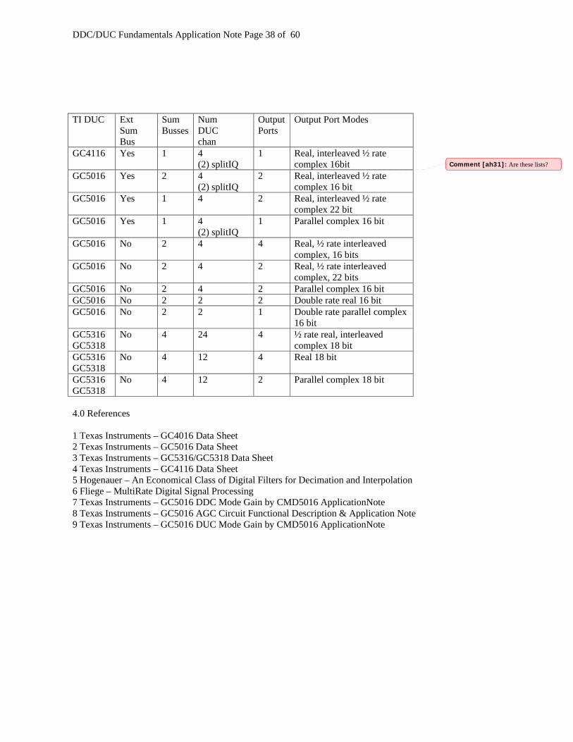
TI DUC Ext
Sum Bus
Sum Busses
Num DUC chan
Output Ports
Output Port Modes
GC4116 Yes 1 4 (2) splitIQ
1 Real, interleaved ½ rate complex 16bit
GC5016 Yes 2 4 (2) splitIQ
2 Real, interleaved ½ rate complex 16 bit
GC5016 Yes 1 4 2 Real, interleaved ½ rate complex 22 bit
GC5016 Yes 1 4 (2) splitIQ
1 Parallel complex 16 bit
GC5016 No 2 4 4 Real, ½ rate interleaved complex, 16 bits
GC5016 No 2 4 2 Real, ½ rate interleaved complex, 22 bits
GC5016 No 2 4 2 Parallel complex 16 bit GC5016 No 2 2 2 Double rate real 16 bit GC5016 No 2 2 1 Double rate parallel complex
16 bit GC5316 GC5318
No 4 24 4 ½ rate real, interleaved complex 18 bit
GC5316 GC5318
No 4 12 4 Real 18 bit
GC5316 GC5318
No 4 12 2 Parallel complex 18 bit
4.0 References 1 Texas Instruments – GC4016 Data Sheet 2 Texas Instruments – GC5016 Data Sheet 3 Texas Instruments – GC5316/GC5318 Data Sheet 4 Texas Instruments – GC4116 Data Sheet 5 Hogenauer – An Economical Class of Digital Filters for Decimation and Interpolation 6 Fliege – MultiRate Digital Signal Processing 7 Texas Instruments – GC5016 DDC Mode Gain by CMD5016 ApplicationNote 8 Texas Instruments – GC5016 AGC Circuit Functional Description & Application Note 9 Texas Instruments – GC5016 DUC Mode Gain by CMD5016 ApplicationNote
Comment [ah31]: Are these lists?
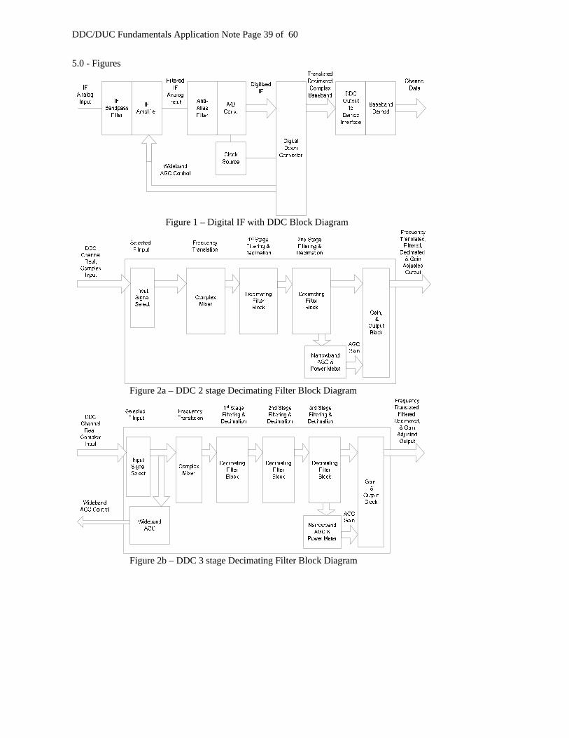
DDC/DUC Fundamentals Application Note Page 39 of 60
5.0 - Figures
Figure 1 – Digital IF with DDC Block Diagram
Figure 2a – DDC 2 stage Decimating Filter Block Diagram
Figure 2b – DDC 3 stage Decimating Filter Block Diagram
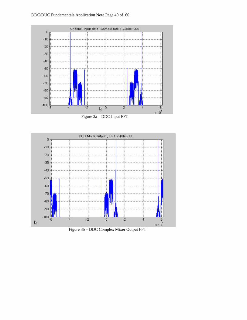
DDC/DUC Fundamentals Application Note Page 40 of 60
Figure 3a – DDC Input FFT
Figure 3b – DDC Complex Mixer Output FFT
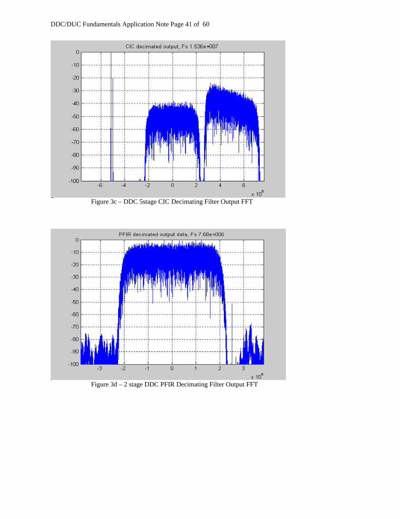
DDC/DUC Fundamentals Application Note Page 41 of 60
Figure 3c – DDC 5stage CIC Decimating Filter Output FFT
Figure 3d – 2 stage DDC PFIR Decimating Filter Output FFT
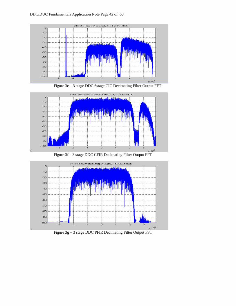
DDC/DUC Fundamentals Application Note Page 42 of 60
Figure 3e – 3 stage DDC 6stage CIC Decimating Filter Output FFT
Figure 3f – 3 stage DDC CFIR Decimating Filter Output FFT
Figure 3g – 3 stage DDC PFIR Decimating Filter Output FFT
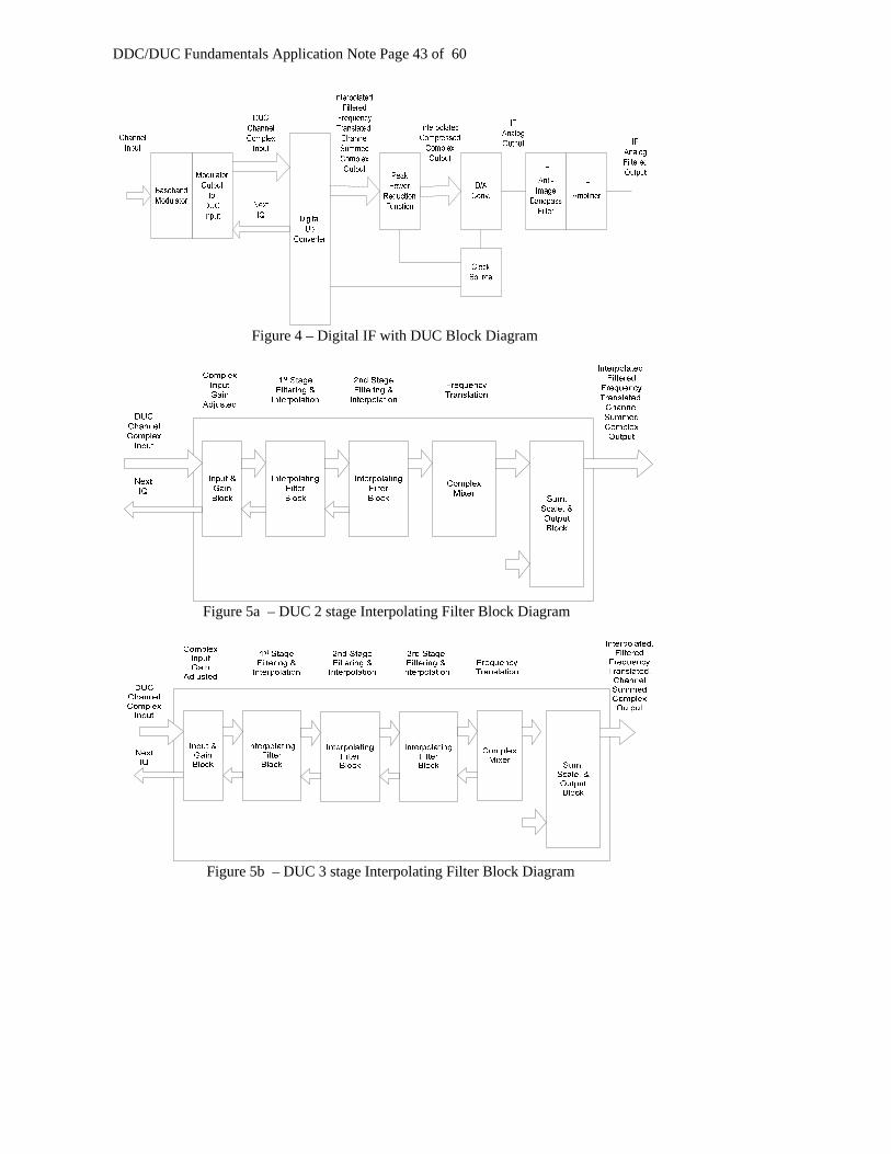
DDC/DUC Fundamentals Application Note Page 43 of 60
Figure 4 – Digital IF with DUC Block Diagram
Figure 5a – DUC 2 stage Interpolating Filter Block Diagram
Figure 5b – DUC 3 stage Interpolating Filter Block Diagram
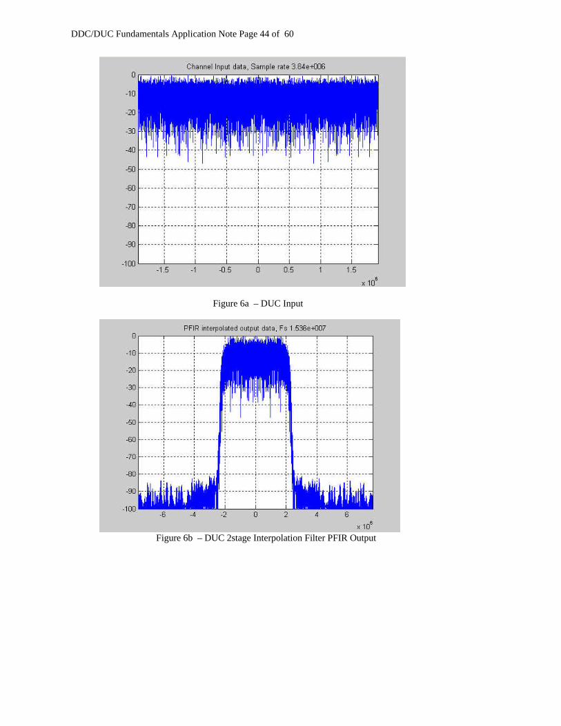
DDC/DUC Fundamentals Application Note Page 44 of 60
Figure 6a – DUC Input
Figure 6b – DUC 2stage Interpolation Filter PFIR Output
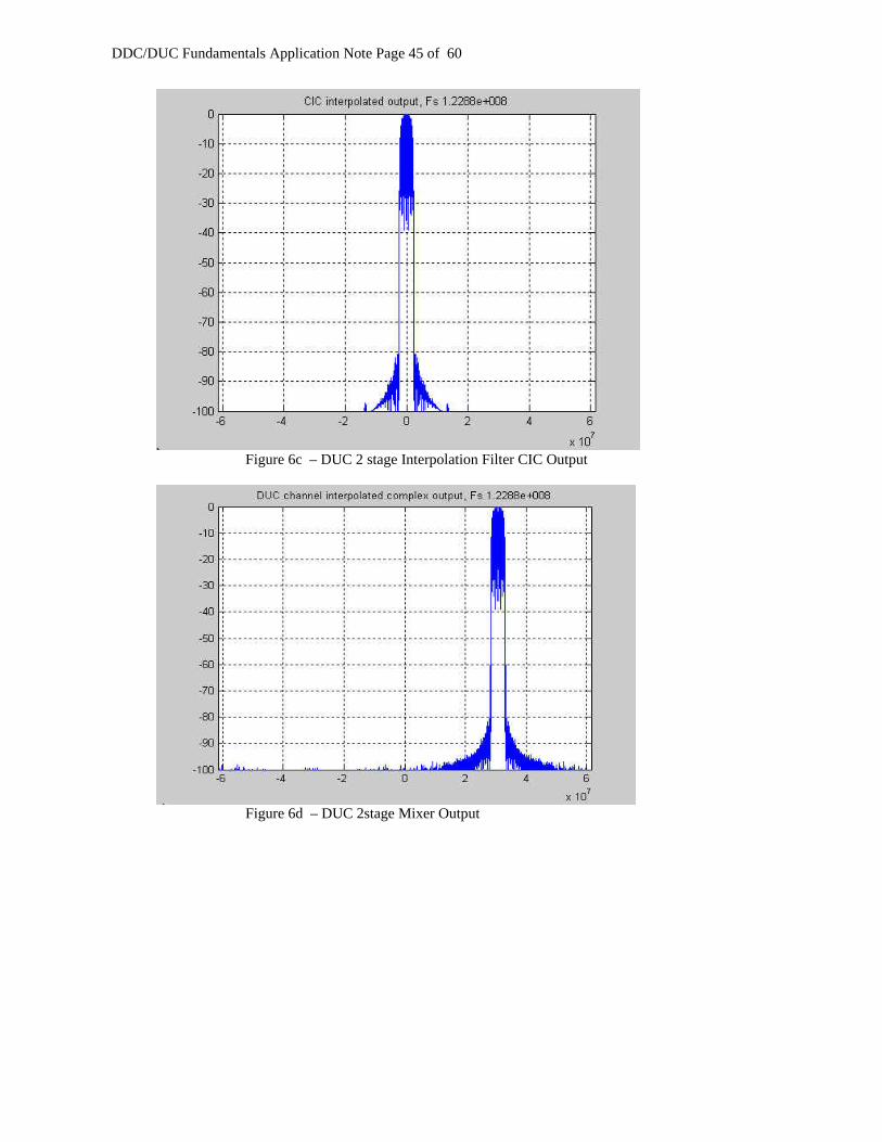
DDC/DUC Fundamentals Application Note Page 45 of 60
Figure 6c – DUC 2 stage Interpolation Filter CIC Output
Figure 6d – DUC 2stage Mixer Output
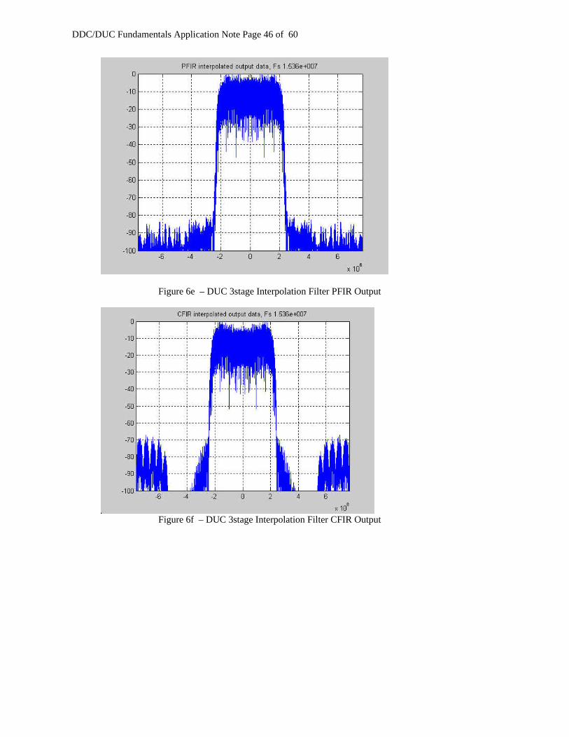
DDC/DUC Fundamentals Application Note Page 46 of 60
Figure 6e – DUC 3stage Interpolation Filter PFIR Output
Figure 6f – DUC 3stage Interpolation Filter CFIR Output
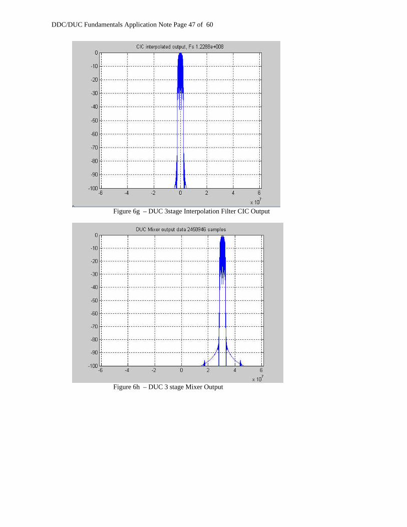
DDC/DUC Fundamentals Application Note Page 47 of 60
Figure 6g – DUC 3stage Interpolation Filter CIC Output
Figure 6h – DUC 3 stage Mixer Output
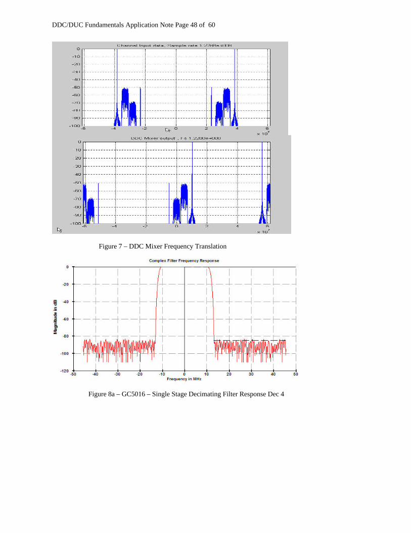
DDC/DUC Fundamentals Application Note Page 48 of 60
Figure 7 – DDC Mixer Frequency Translation
Figure 8a – GC5016 – Single Stage Decimating Filter Response Dec 4
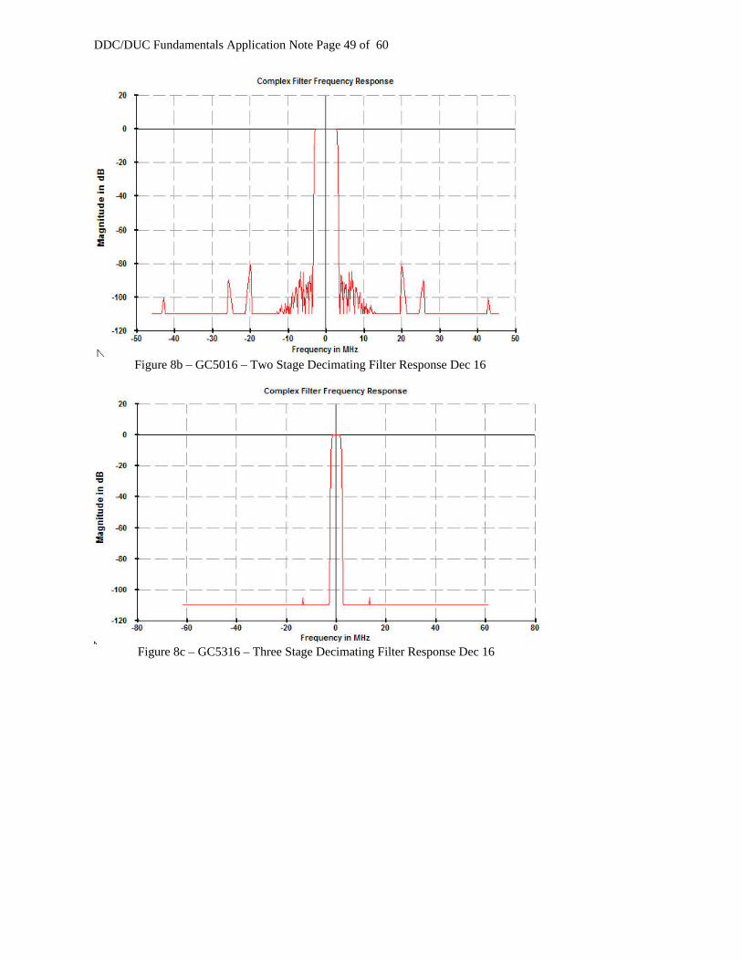
DDC/DUC Fundamentals Application Note Page 49 of 60
Figure 8b – GC5016 – Two Stage Decimating Filter Response Dec 16
Figure 8c – GC5316 – Three Stage Decimating Filter Response Dec 16
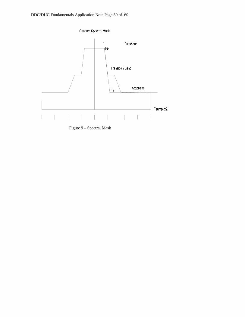
DDC/DUC Fundamentals Application Note Page 50 of 60
Figure 9 – Spectral Mask
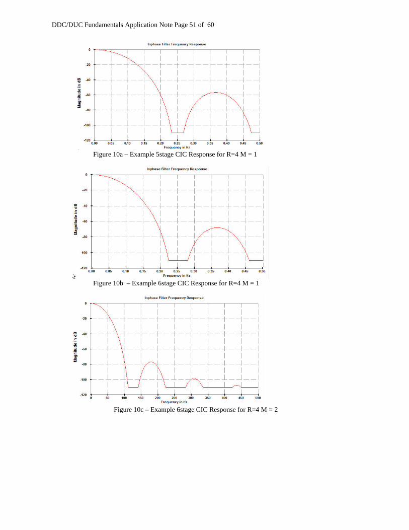
DDC/DUC Fundamentals Application Note Page 51 of 60
Figure 10a – Example 5stage CIC Response for R=4 M = 1
Figure 10b – Example 6stage CIC Response for R=4 M = 1
Figure 10c – Example 6stage CIC Response for R=4 M = 2
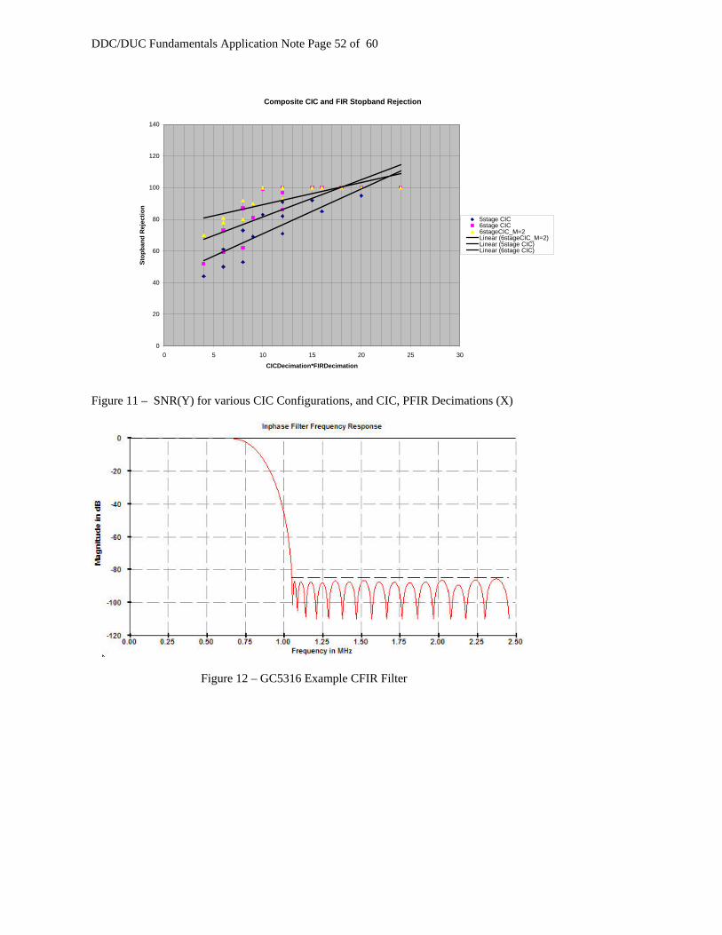
DDC/DUC Fundamentals Application Note Page 52 of 60
Composite CIC and FIR Stopband Rejection
0
20
40
60
80
100
120
140
0 5 10 15 20 25 30
CICDecimation*FIRDecimation
Stop
band
Rej
ectio
n
5stage CIC6stage CIC6stageCIC_M=2Linear (6stageCIC_M=2)Linear (5stage CIC)Linear (6stage CIC)
Figure 11 – SNR(Y) for various CIC Configurations, and CIC, PFIR Decimations (X)
Figure 12 – GC5316 Example CFIR Filter
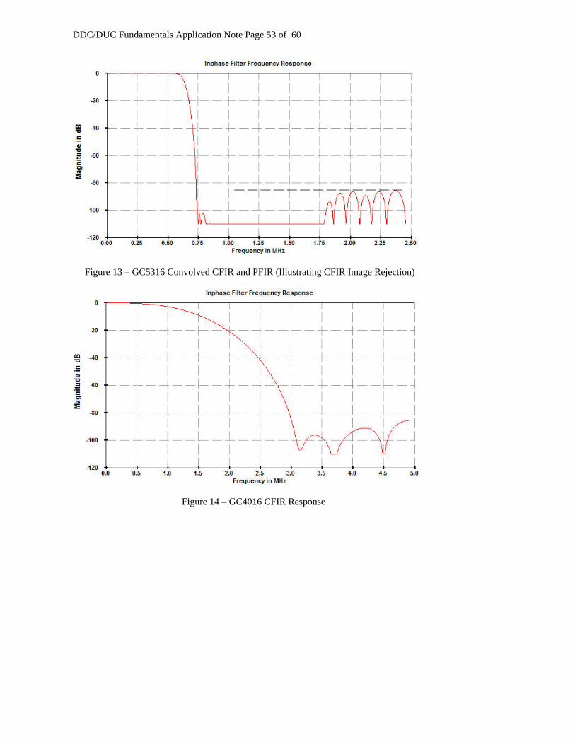
DDC/DUC Fundamentals Application Note Page 53 of 60
Figure 13 – GC5316 Convolved CFIR and PFIR (Illustrating CFIR Image Rejection)
Figure 14 – GC4016 CFIR Response
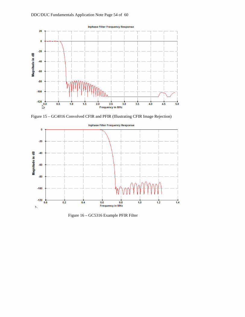
DDC/DUC Fundamentals Application Note Page 54 of 60
Figure 15 – GC4016 Convolved CFIR and PFIR (Illustrating CFIR Image Rejection)
Figure 16 – GC5316 Example PFIR Filter
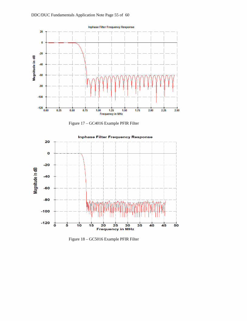
DDC/DUC Fundamentals Application Note Page 55 of 60
Figure 17 – GC4016 Example PFIR Filter
Figure 18 – GC5016 Example PFIR Filter
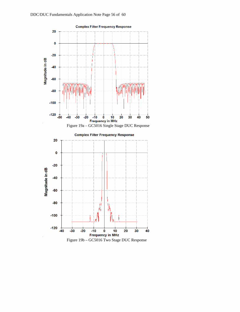
DDC/DUC Fundamentals Application Note Page 56 of 60
Figure 19a – GC5016 Single Stage DUC Response
Figure 19b – GC5016 Two Stage DUC Response
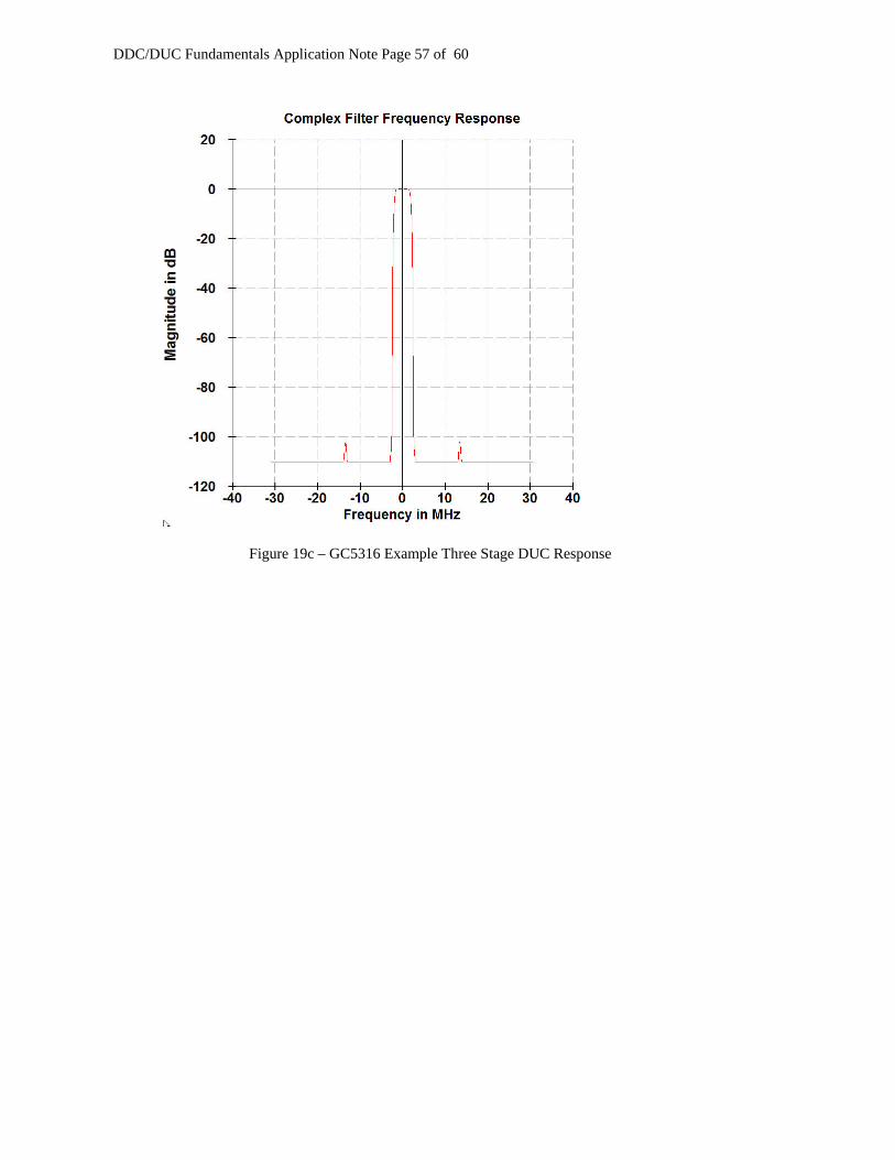
DDC/DUC Fundamentals Application Note Page 57 of 60
Figure 19c – GC5316 Example Three Stage DUC Response
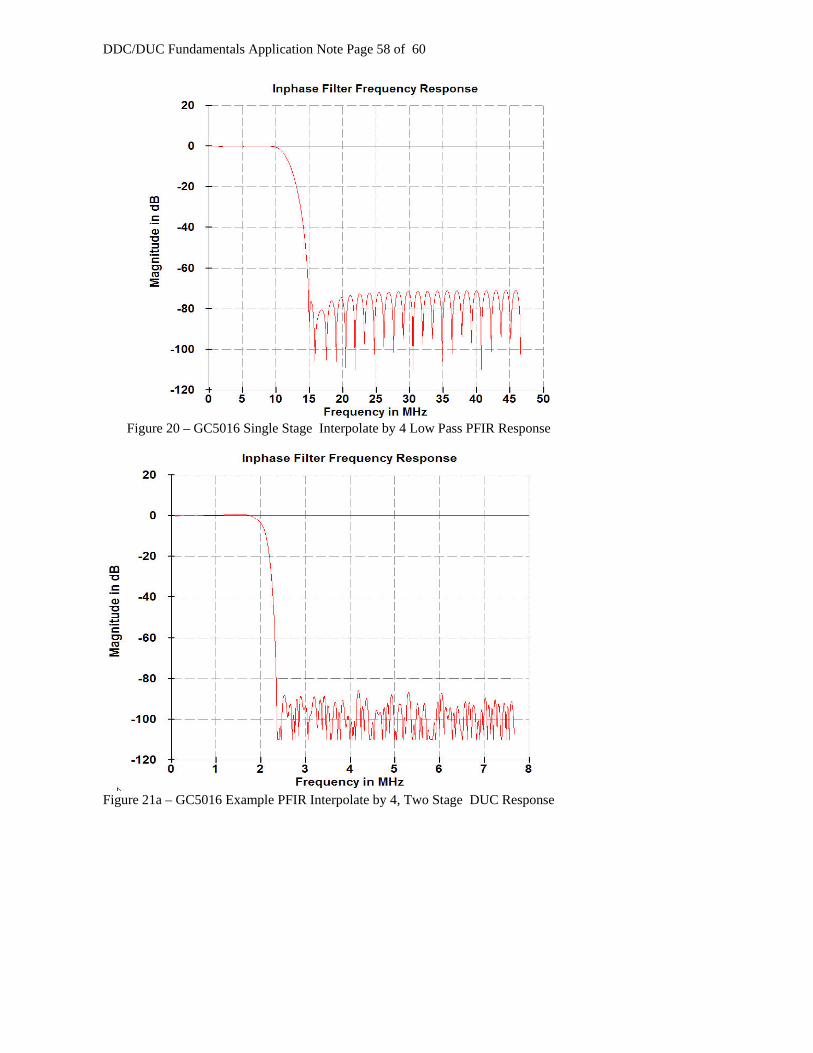
DDC/DUC Fundamentals Application Note Page 58 of 60
Figure 20 – GC5016 Single Stage Interpolate by 4 Low Pass PFIR Response
Figure 21a – GC5016 Example PFIR Interpolate by 4, Two Stage DUC Response
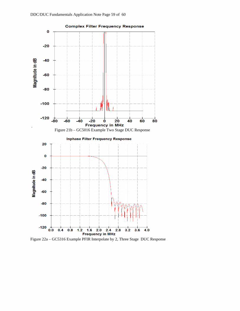
DDC/DUC Fundamentals Application Note Page 59 of 60
Figure 21b – GC5016 Example Two Stage DUC Response
Figure 22a – GC5316 Example PFIR Interpolate by 2, Three Stage DUC Response
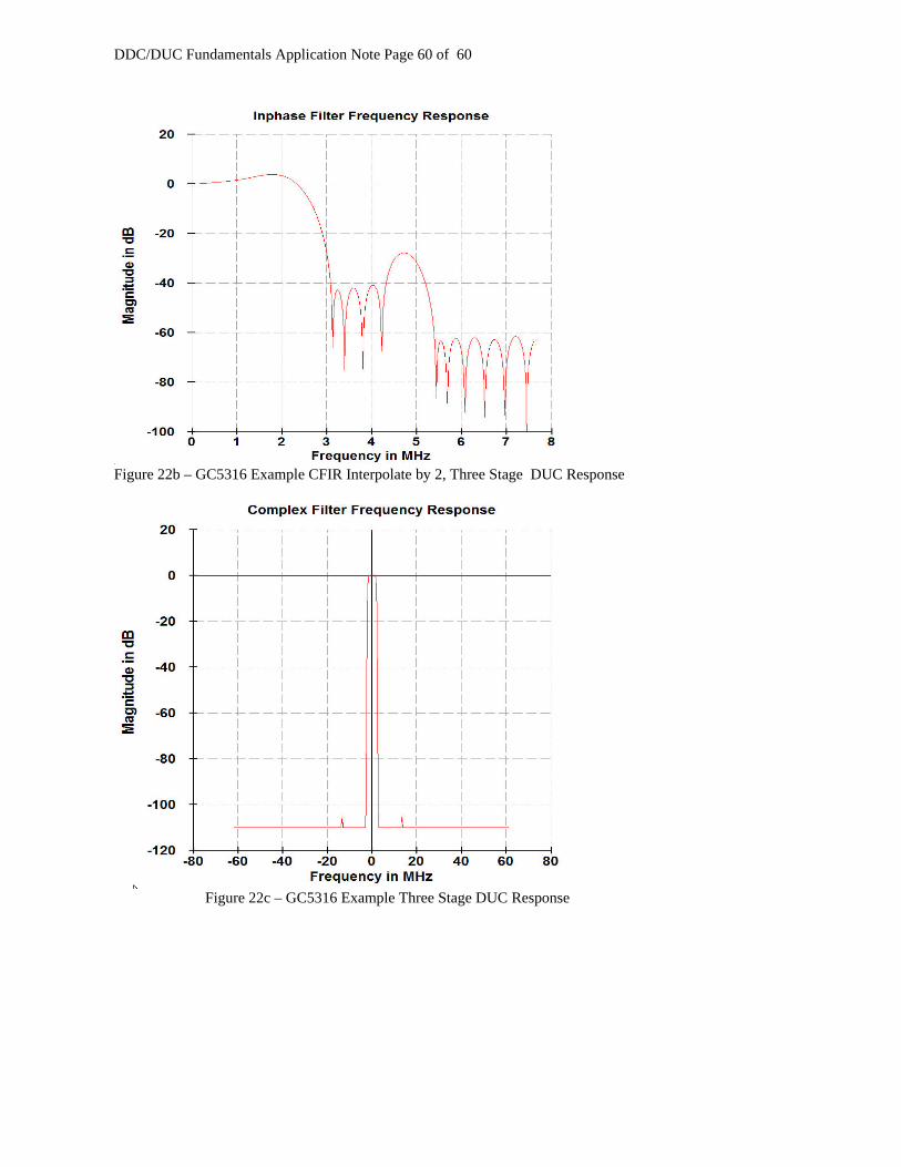
DDC/DUC Fundamentals Application Note Page 60 of 60
Figure 22b – GC5316 Example CFIR Interpolate by 2, Three Stage DUC Response
Figure 22c – GC5316 Example Three Stage DUC Response
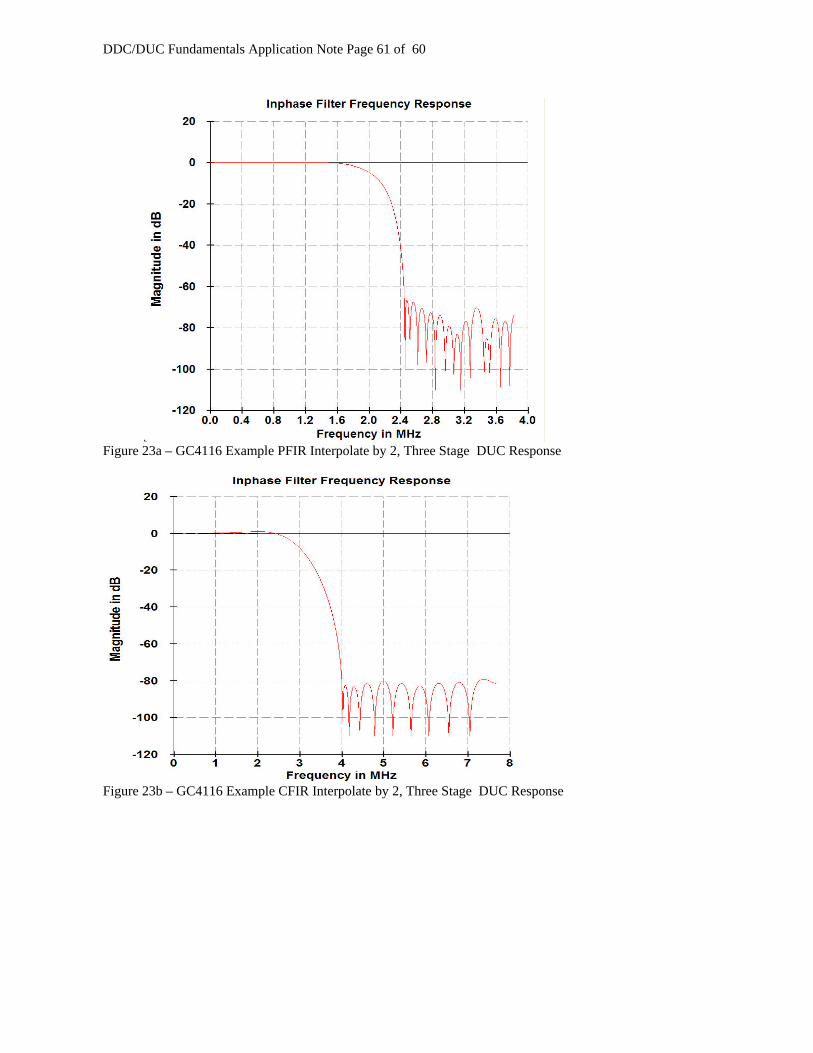
DDC/DUC Fundamentals Application Note Page 61 of 60
Figure 23a – GC4116 Example PFIR Interpolate by 2, Three Stage DUC Response
Figure 23b – GC4116 Example CFIR Interpolate by 2, Three Stage DUC Response
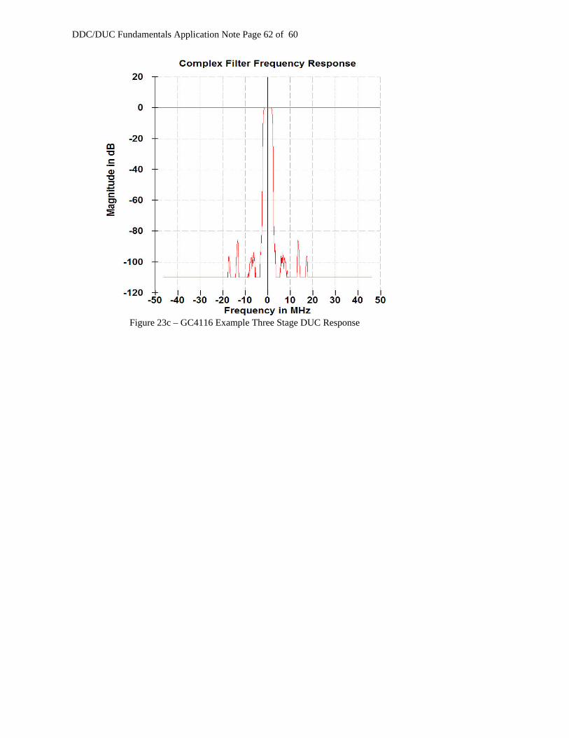
DDC/DUC Fundamentals Application Note Page 62 of 60
Figure 23c – GC4116 Example Three Stage DUC Response
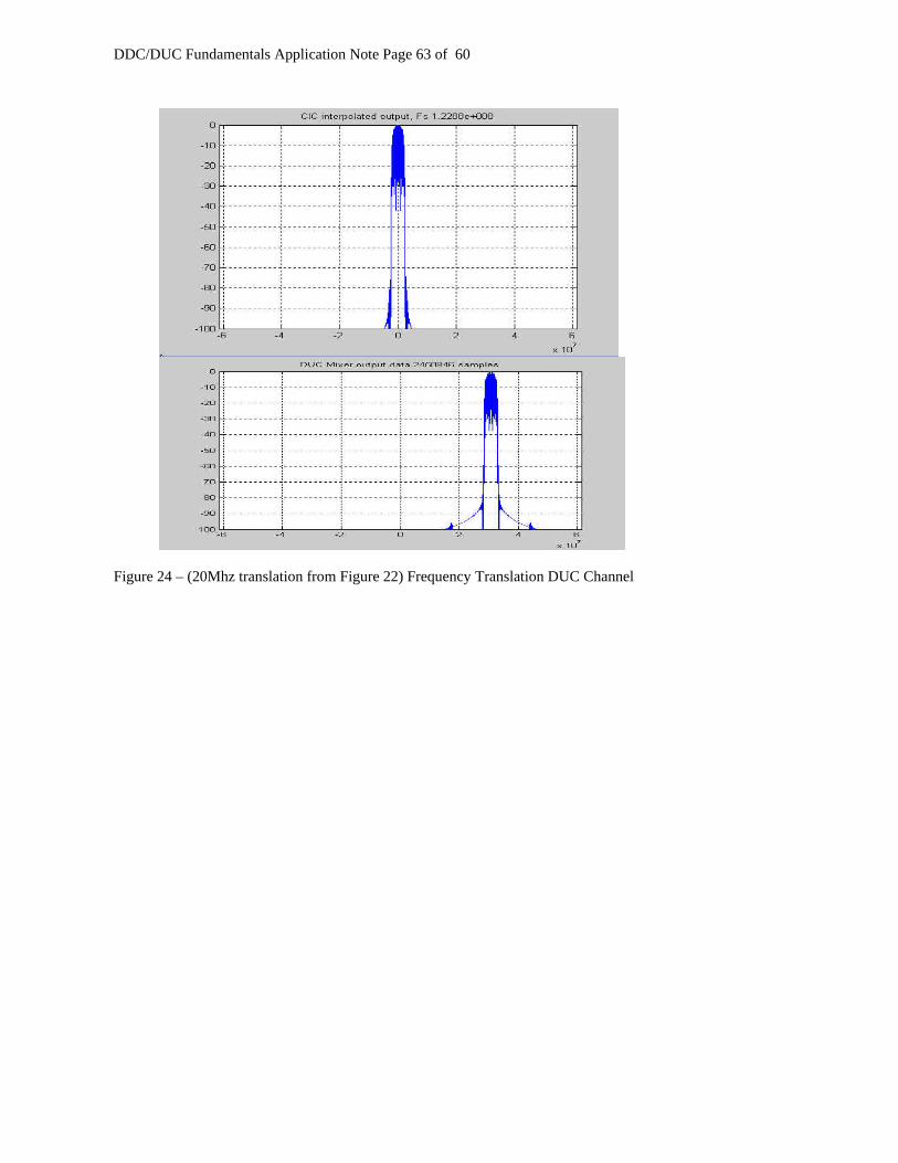
DDC/DUC Fundamentals Application Note Page 63 of 60
Figure 24 – (20Mhz translation from Figure 22) Frequency Translation DUC Channel