Embed Size (px)
Citation preview
Datasheet
Product structure:Silicon monolithic integrated circuit This product has no designed protection against radioactive rays .
1/17 © 2014 ROHM Co., Ltd. All rights reserved. www.rohm.com
TSZ22111・14・001 TSZ02201-0H1H0B101050-1-2
5.Jun.2014 Rev.001
DC Brushless Motor Drivers for Fans
Standard Single-phase Full wave Fan Motor Driver BD69830FV
Description
The BD69830FV is a 24V single-coil brushless DC FAN motor driver. The device incorporates high efficiency DMOS H-bridge driver, regulated voltage output for hall element, and rotation speed is controlled by input PWM signal.
Features
Power DMOS FET integrated Direct PWM speed control Low duty start up function Quick start function Constant voltage output for hall element Lock protection and auto restart
(without external capacitor) Rotating speed pulse signal (FG) output
and ALARM signal output selectable
Applications BD player, Projector, STB etc,. Office equipment, Copier, FAX, Laser Printer, etc,.
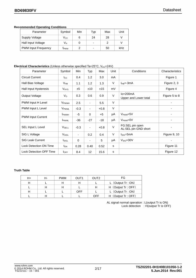
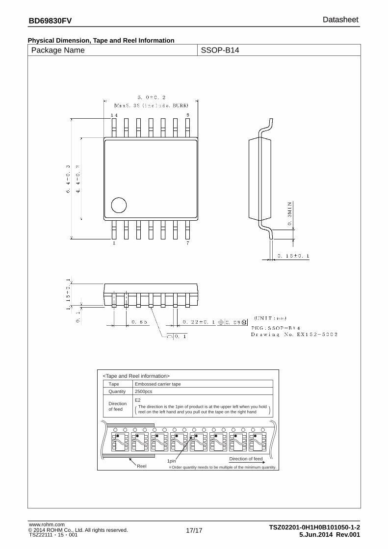
Package W(Typ) x D(Typ) x H(Max) SSOP-B14 5.00mm x 6.40mm x 1.35mm
Absolute Maximum Ratings
Parameter Symbol Rating Unit
Supply Voltage VCC 30 V
Power Dissipation Pd 0.87(Note 1) W
Operating Temperature Topr -40 to +105 °C
Storage Temperature Tstg -55 to +150 °C
Junction Temperature Tjmax 150 °C
Output Voltage VOMAX 30 V
Output Current IOMAX 900(Note 2) mA
Hall Input Voltage VH 7 V
PWM Input Voltage VPWM 7 V
SEL Input Voltage VSEL 7 V
Signal Output Voltage VSIG 30 V
Signal Output Current ISIG 10 mA
HB Current Ability IHB 10 mA (Note 1) Reduce by 7.0mW/ over 25. (On 70.0mm×70.0mm×1.6mm glass epoxy board) (Note 2) This value is not to exceed Pd.
Caution: Operating the IC over the absolute maximum ratings may damage the IC. The damage can either be a short circuit between pins or an open circuit between pins and the internal circuitry. Therefore, it is important to consider circuit protection measures, such as adding a fuse, in case the IC is operated over the absolute maximum ratings.
SSOP-B14
DatasheetDatasheet
2/17 www.rohm.com © 2014 ROHM Co., Ltd. All rights reserved. TSZ22111・15・001
TSZ02201-0H1H0B101050-1-25.Jun.2014 Rev.001
BD69830FV
Recommended Operating Conditions
Parameter Symbol Min Typ Max Unit
Supply Voltage VCC 6 24 28 V
Hall Input Voltage VH 0 - 2 V
PWM Input Frequency fPWM 2 - 50 kHz Electrical Characteristics (Unless otherwise specified Ta=25°C, VCC=24V)
Parameter Symbol Min Typ Max Unit Conditions Characteristics
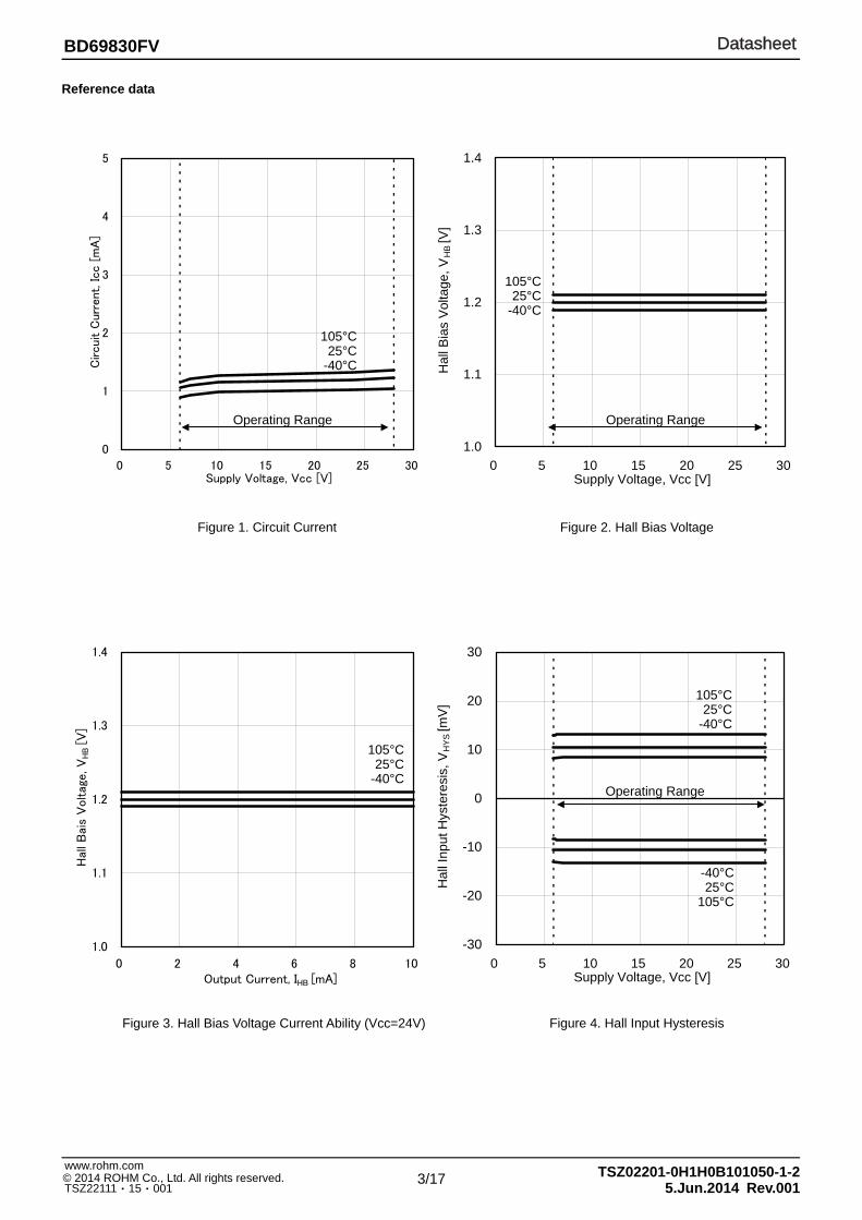
Circuit Current ICC 0.4 1.2 3.0 mA Figure 1
Hall Bias Voltage VHB 1.1 1.2 1.3 V IHB=-3mA Figure 2, 3
Hall Input Hysteresis VHYS ±5 ±10 ±15 mV Figure 4
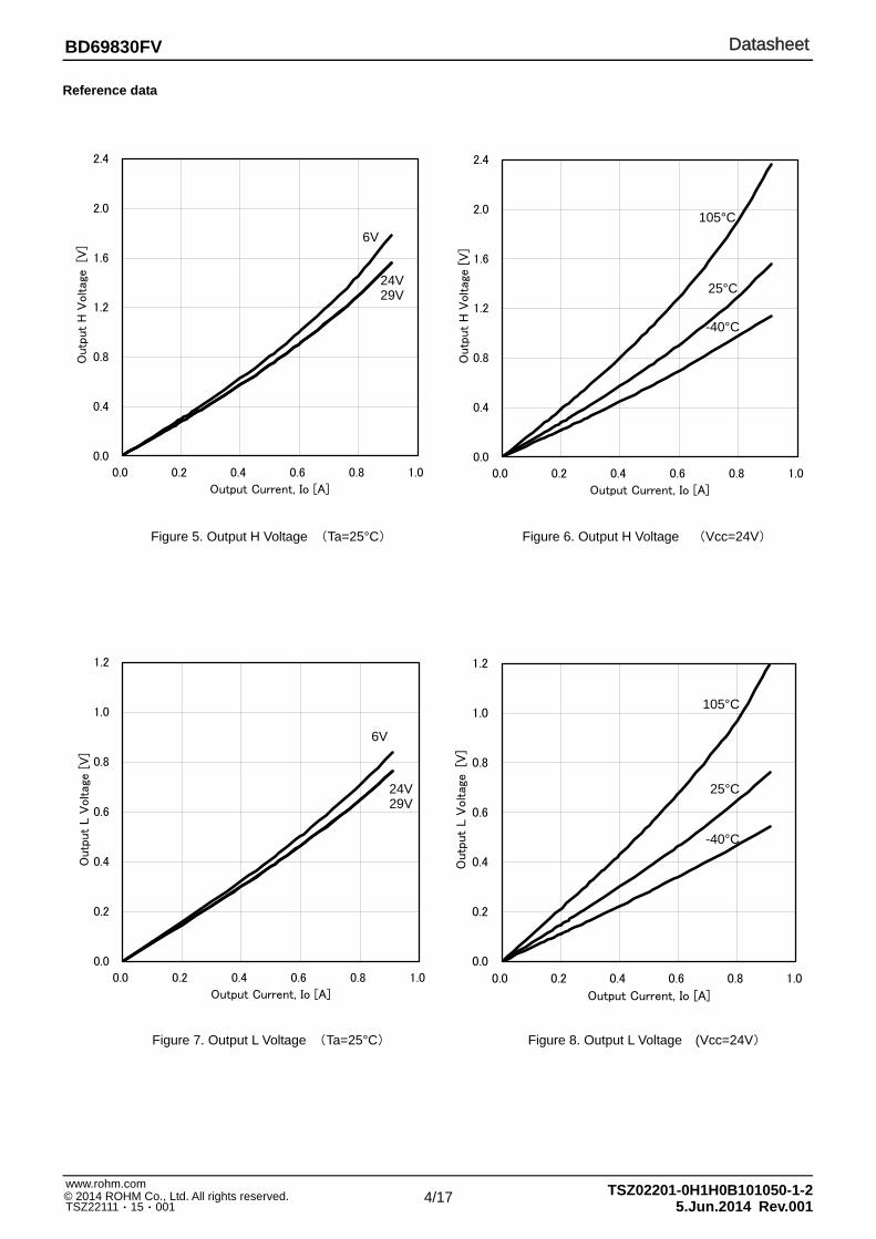
Output Voltage VO 0.3 0.6 0.9 V Io=200mA Upper and Lower total
Figure 5 to 8
PWM Input H Level VPWMH 2.5 - 5.5 V -
PWM Input L Level VPWML -0.3 - +0.8 V -
IPWMH -5 0 +5 µA VPWM=5V - PWM Input Current
IPWML -36 -27 -18 µA VPWM=0V -
SEL Input L Level VSELL -0.3 - +0.8 V FG:SEL pin open AL:SEL pin GND short -
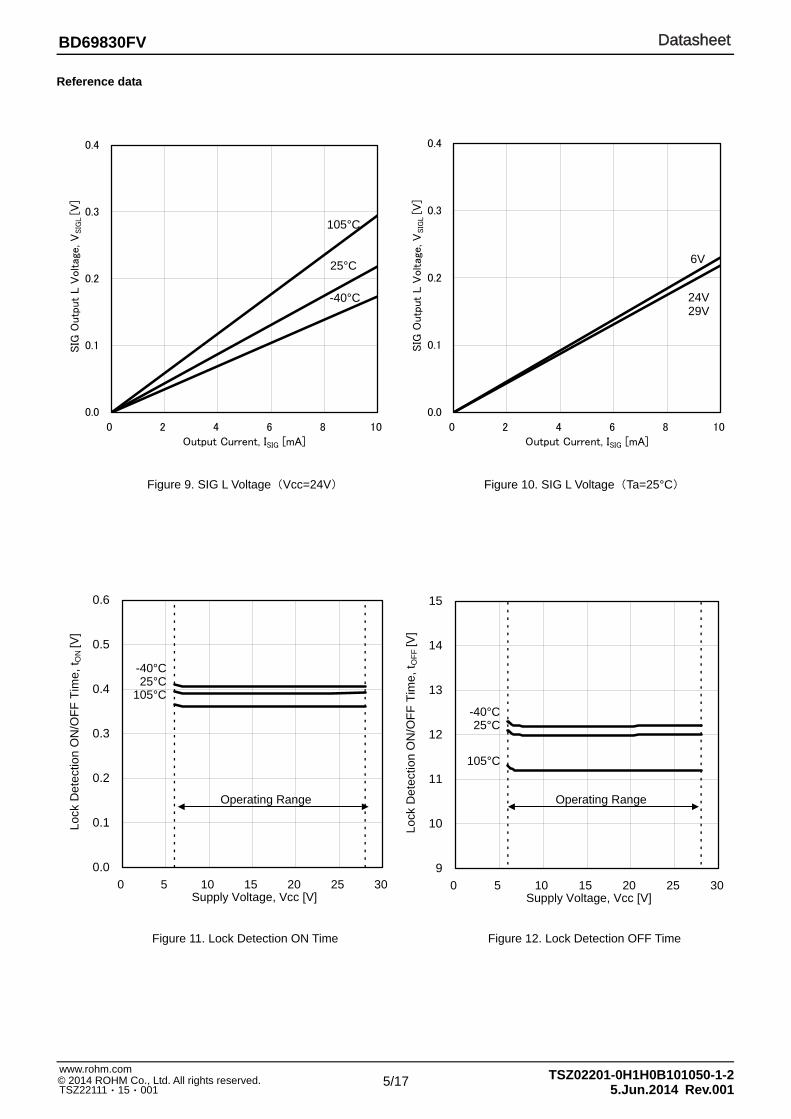
SIG L Voltage VSIGL - 0.2 0.4 V ISIG=5mA Figure 9, 10
SIG Leak Current ISIGL 0 - 5 µA VSIG=30V -
Lock Detection ON Time tON 0.28 0.40 0.52 s Figure 11
Lock Detection OFF Time tOFF 8.4 12 15.6 s Figure 12
Truth Table
H+ H- PWM OUT1 OUT2 FG
H L H H L L(Output Tr : ON) L H H L H H(Output Tr : OFF) H L L OFF L L(Output Tr : ON) L H L L OFF H(Output Tr : OFF)
AL signal normal operation : L(output Tr is ON) Lock detection : H(output Tr is OFF)
DatasheetDatasheet
3/17 www.rohm.com © 2014 ROHM Co., Ltd. All rights reserved. TSZ22111・15・001
TSZ02201-0H1H0B101050-1-25.Jun.2014 Rev.001
BD69830FV
Reference data
1.0
1.1
1.2
1.3
1.4
0 2 4 6 8 10Output Current, IHB [mA]
Hal
l B
ais
Voltag
e, V
HB
[V
]
-30
-20
-10
0
10
20
30
0 5 10 15 20 25 30Supply Voltage, Vcc [V]
Hal
l Inp
ut H
yste
resi
s, V
HY
S [m
V]
1.0
1.1
1.2
1.3
1.4
0 5 10 15 20 25 30Supply Voltage, Vcc [V]
Hal
l Bia
s V
olta
ge, V
HB
[V]
105°C25°C
-40°C
0
1
2
3
4
5
0 5 10 15 20 25 30Supply Voltage, Vcc [V]
Circuit C
urr
ent, Icc [
mA
]
Figure 1. Circuit Current
Figure 3. Hall Bias Voltage Current Ability (Vcc=24V) Figure 4. Hall Input Hysteresis
Figure 2. Hall Bias Voltage
Operating Range
105°C25°C
-40°C
105°C25°C
-40°C
105°C25°C
-40°C
Operating Range
-40°C25°C
105°C
Operating Range
DatasheetDatasheet
4/17 www.rohm.com © 2014 ROHM Co., Ltd. All rights reserved. TSZ22111・15・001
TSZ02201-0H1H0B101050-1-25.Jun.2014 Rev.001
BD69830FV
Reference data
0.0
0.4
0.8
1.2
1.6
2.0
2.4
0.0 0.2 0.4 0.6 0.8 1.0
Output Current, Io [A]
Outp
ut
H V
oltag
e [
V]
0.0
0.4
0.8
1.2
1.6
2.0
2.4
0.0 0.2 0.4 0.6 0.8 1.0
Output Current, Io [A]
Outp
ut
H V
oltag
e [V
]
0.0
0.2
0.4
0.6
0.8
1.0
1.2
0.0 0.2 0.4 0.6 0.8 1.0
Output Current, Io [A]
Outp
ut
L V
oltag
e [V
]
0.0
0.2
0.4
0.6
0.8
1.0
1.2
0.0 0.2 0.4 0.6 0.8 1.0
Output Current, Io [A]
Outp
ut
L V
oltag
e [
V]
Figure 5. Output H Voltage (Ta=25°C) Figure 6. Output H Voltage (Vcc=24V)
Figure 7. Output L Voltage (Ta=25°C)
Figure 8. Output L Voltage (Vcc=24V)
105°C
105°C
6V
24V29V
25°C
-40°C
6V
24V29V 25°C
-40°C
DatasheetDatasheet
5/17 www.rohm.com © 2014 ROHM Co., Ltd. All rights reserved. TSZ22111・15・001
TSZ02201-0H1H0B101050-1-25.Jun.2014 Rev.001
BD69830FV
Reference data
9
10
11
12
13
14
15
0 5 10 15 20 25 30Supply Voltage, Vcc [V]
Lock
Det
ectio
n O
N/O
FF T
ime,
t OFF
[V]
0.0
0.1
0.2
0.3
0.4
0.5
0.6
0 5 10 15 20 25 30Supply Voltage, Vcc [V]
Lock
Det
ectio
n O
N/O
FF T
ime,
t ON
[V]
Figure 11. Lock Detection ON Time
Figure 12. Lock Detection OFF Time
Figure 9. SIG L Voltage(Vcc=24V)
Figure 10. SIG L Voltage(Ta=25°C)
0.0
0.1
0.2
0.3
0.4
0 2 4 6 8 10
Output Current, ISIG [mA]
SIG
Outp
ut
L V
oltag
e, V
SIG
L [V
]
105°C
25°C
-40°C
0.0
0.1
0.2
0.3
0.4
0 2 4 6 8 10
Output Current, ISIG [mA]
SIG
Outp
ut
L V
oltag
e, V
SIG
L [V
]
6V
24V29V
-40°C25°C
105°C
105°C
-40°C25°C
Operating Range Operating Range
DatasheetDatasheet
6/17 www.rohm.com © 2014 ROHM Co., Ltd. All rights reserved. TSZ22111・15・001
TSZ02201-0H1H0B101050-1-25.Jun.2014 Rev.001
BD69830FV
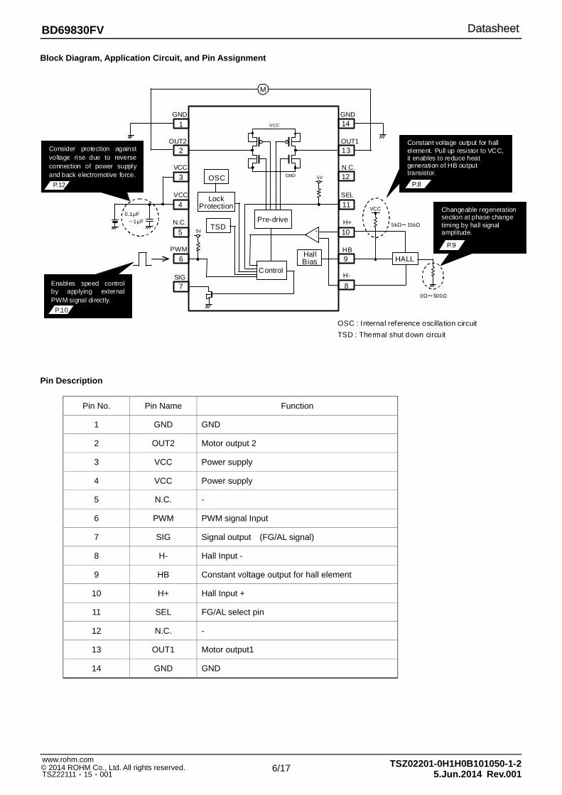
Block Diagram, Application Circuit, and Pin Assignment Pin Description
Pin No. Pin Name Function
1 GND GND
2 OUT2 Motor output 2
3 VCC Power supply
4 VCC Power supply
5 N.C. -
6 PWM PWM signal Input
7 SIG Signal output (FG/AL signal)
8 H- Hall Input -
9 HB Constant voltage output for hall element
10 H+ Hall Input +
11 SEL FG/AL select pin
12 N.C. -
13 OUT1 Motor output1
14 GND GND
OSC : Internal reference oscillation circuit TSD : Thermal shut down circuit
Enables speed control by applying external PWM signal directly.
P.10
Consider protection against voltage rise due to reverse connection of power supply and back electromotive force.
OUT2
VCC
VCC
GND 1
2
3
4
14
13
12
11 Lock Protection
OUT1
N.C.
SEL
GND
OSC
N.C. 5 10
SIG
HallBias
Control
-+5V
5V
TSD Pre-drive
GND
VCC
HALL 6
7
9
8H-
HB
H+
PWM
5kΩ~15kΩ
VCC0.1µF ~1µF
M
P.12
0Ω~500Ω
Constant voltage output for hall element. Pull up resistor to VCC, it enables to reduce heat generation of HB output transistor.
Changeable regeneration section at phase change timing by hall signal amplitude.
P.9
P.8
DatasheetDatasheet
7/17 www.rohm.com © 2014 ROHM Co., Ltd. All rights reserved. TSZ22111・15・001
TSZ02201-0H1H0B101050-1-25.Jun.2014 Rev.001
BD69830FV
H+
tOFF
FG
tON
Idling
OUT1
OUT2
AL
Recovers normal operation
Output Tr OFF ON
Depends on hall signal(H in ths figure)
Motor lock
Lockdetection
Lockrelease
tON
(at SEL=open)
(at SEL=GND)
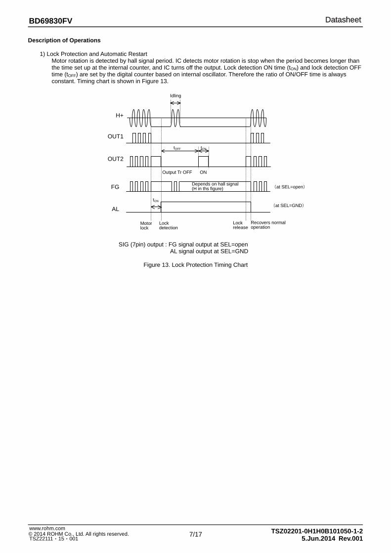
Description of Operations 1) Lock Protection and Automatic Restart
Motor rotation is detected by hall signal period. IC detects motor rotation is stop when the period becomes longer than the time set up at the internal counter, and IC turns off the output. Lock detection ON time (tON) and lock detection OFF time (tOFF) are set by the digital counter based on internal oscillator. Therefore the ratio of ON/OFF time is always constant. Timing chart is shown in Figure 13.
SIG (7pin) output : FG signal output at SEL=open AL signal output at SEL=GND
Figure 13. Lock Protection Timing Chart
DatasheetDatasheet
8/17 www.rohm.com © 2014 ROHM Co., Ltd. All rights reserved. TSZ22111・15・001
TSZ02201-0H1H0B101050-1-25.Jun.2014 Rev.001
BD69830FV
Hall element
IC
VCC
GND
HB
IC
VCC
GND
HB
R1
RH
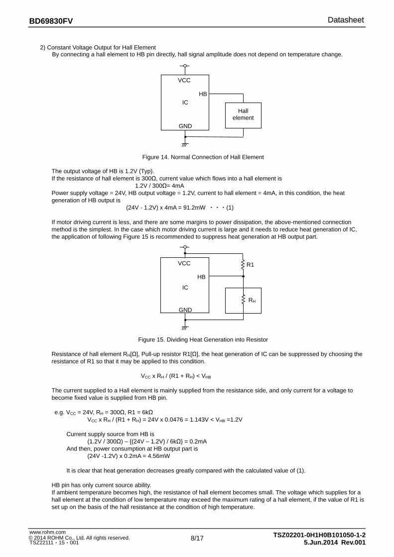
2) Constant Voltage Output for Hall Element
By connecting a hall element to HB pin directly, hall signal amplitude does not depend on temperature change.
Figure 14. Normal Connection of Hall Element
The output voltage of HB is 1.2V (Typ). If the resistance of hall element is 300Ω, current value which flows into a hall element is 1.2V / 300Ω= 4mA Power supply voltage = 24V, HB output voltage = 1.2V, current to hall element = 4mA, in this condition, the heat generation of HB output is (24V - 1.2V) x 4mA = 91.2mW ・・・(1) If motor driving current is less, and there are some margins to power dissipation, the above-mentioned connection method is the simplest. In the case which motor driving current is large and it needs to reduce heat generation of IC, the application of following Figure 15 is recommended to suppress heat generation at HB output part.
Figure 15. Dividing Heat Generation into Resistor Resistance of hall element RH[Ω], Pull-up resistor R1[Ω], the heat generation of IC can be suppressed by choosing the resistance of R1 so that it may be applied to this condition. VCC x RH / (R1 + RH) < VHB The current supplied to a Hall element is mainly supplied from the resistance side, and only current for a voltage to become fixed value is supplied from HB pin. e.g. VCC = 24V, RH = 300Ω, R1 = 6kΩ VCC x RH / (R1 + RH) = 24V x 0.0476 = 1.143V < VHB =1.2V Current supply source from HB is (1.2V / 300Ω) – (24V – 1.2V) / 6kΩ = 0.2mA And then, power consumption at HB output part is (24V -1.2V) x 0.2mA = 4.56mW It is clear that heat generation decreases greatly compared with the calculated value of (1). HB pin has only current source ability. If ambient temperature becomes high, the resistance of hall element becomes small. The voltage which supplies for a hall element at the condition of low temperature may exceed the maximum rating of a hall element, if the value of R1 is set up on the basis of the hall resistance at the condition of high temperature.
DatasheetDatasheet
9/17 www.rohm.com © 2014 ROHM Co., Ltd. All rights reserved. TSZ22111・15・001
TSZ02201-0H1H0B101050-1-25.Jun.2014 Rev.001
BD69830FV
2V
GND H
all i
nput
vol
tage
rang
e
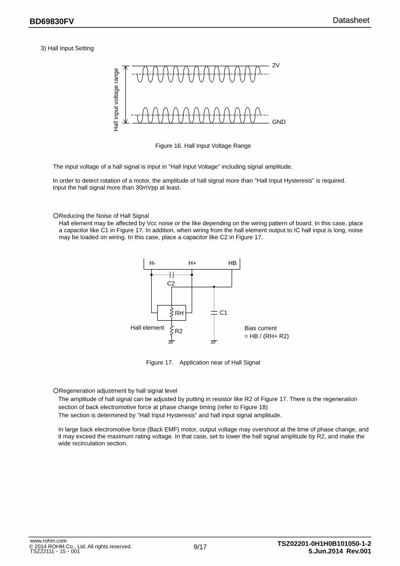
3) Hall Input Setting
Figure 16. Hall Input Voltage Range
The input voltage of a hall signal is input in "Hall Input Voltage" including signal amplitude. In order to detect rotation of a motor, the amplitude of hall signal more than "Hall Input Hysteresis" is required. Input the hall signal more than 30mVpp at least. Reducing the Noise of Hall Signal
Hall element may be affected by Vcc noise or the like depending on the wiring pattern of board. In this case, place a capacitor like C1 in Figure 17. In addition, when wiring from the hall element output to IC hall input is long, noise may be loaded on wiring. In this case, place a capacitor like C2 in Figure 17.
Figure 17. Application near of Hall Signal Regeneration adjustment by hall signal level
The amplitude of hall signal can be adjusted by putting in resistor like R2 of Figure 17. There is the regeneration section of back electromotive force at phase change timing (refer to Figure 18) The section is determined by "Hall Input Hysteresis" and hall input signal amplitude. In large back electromotive force (Back EMF) motor, output voltage may overshoot at the time of phase change, and it may exceed the maximum rating voltage. In that case, set to lower the hall signal amplitude by R2, and make the wide recirculation section.
C2
Hall element
H- H+ HB
R2
RH C1
Bias current = HB / (RH+ R2)
DatasheetDatasheet
10/17 www.rohm.com © 2014 ROHM Co., Ltd. All rights reserved. TSZ22111・15・001
TSZ02201-0H1H0B101050-1-25.Jun.2014 Rev.001
BD69830FV
H+
PWM
OUT1
OUT2
FG
Hall input hysteresis
Output duty=80%
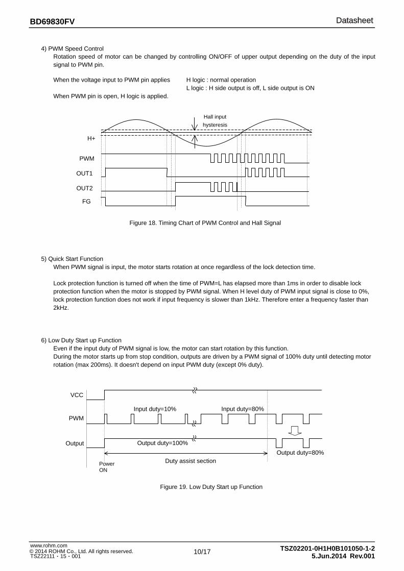
4) PWM Speed Control
Rotation speed of motor can be changed by controlling ON/OFF of upper output depending on the duty of the input signal to PWM pin.
When the voltage input to PWM pin applies H logic : normal operation L logic : H side output is off, L side output is ON When PWM pin is open, H logic is applied.
Figure 18. Timing Chart of PWM Control and Hall Signal 5) Quick Start Function
When PWM signal is input, the motor starts rotation at once regardless of the lock detection time. Lock protection function is turned off when the time of PWM=L has elapsed more than 1ms in order to disable lock protection function when the motor is stopped by PWM signal. When H level duty of PWM input signal is close to 0%, lock protection function does not work if input frequency is slower than 1kHz. Therefore enter a frequency faster than 2kHz.
6) Low Duty Start up Function Even if the input duty of PWM signal is low, the motor can start rotation by this function. During the motor starts up from stop condition, outputs are driven by a PWM signal of 100% duty until detecting motor rotation (max 200ms). It doesn't depend on input PWM duty (except 0% duty).
Figure 19. Low Duty Start up Function
Input duty=80%
VCC
Duty assist section PowerON
PWM
Output
Input duty=10%
Output duty=100%
DatasheetDatasheet
11/17 www.rohm.com © 2014 ROHM Co., Ltd. All rights reserved. TSZ22111・15・001
TSZ02201-0H1H0B101050-1-25.Jun.2014 Rev.001
BD69830FV
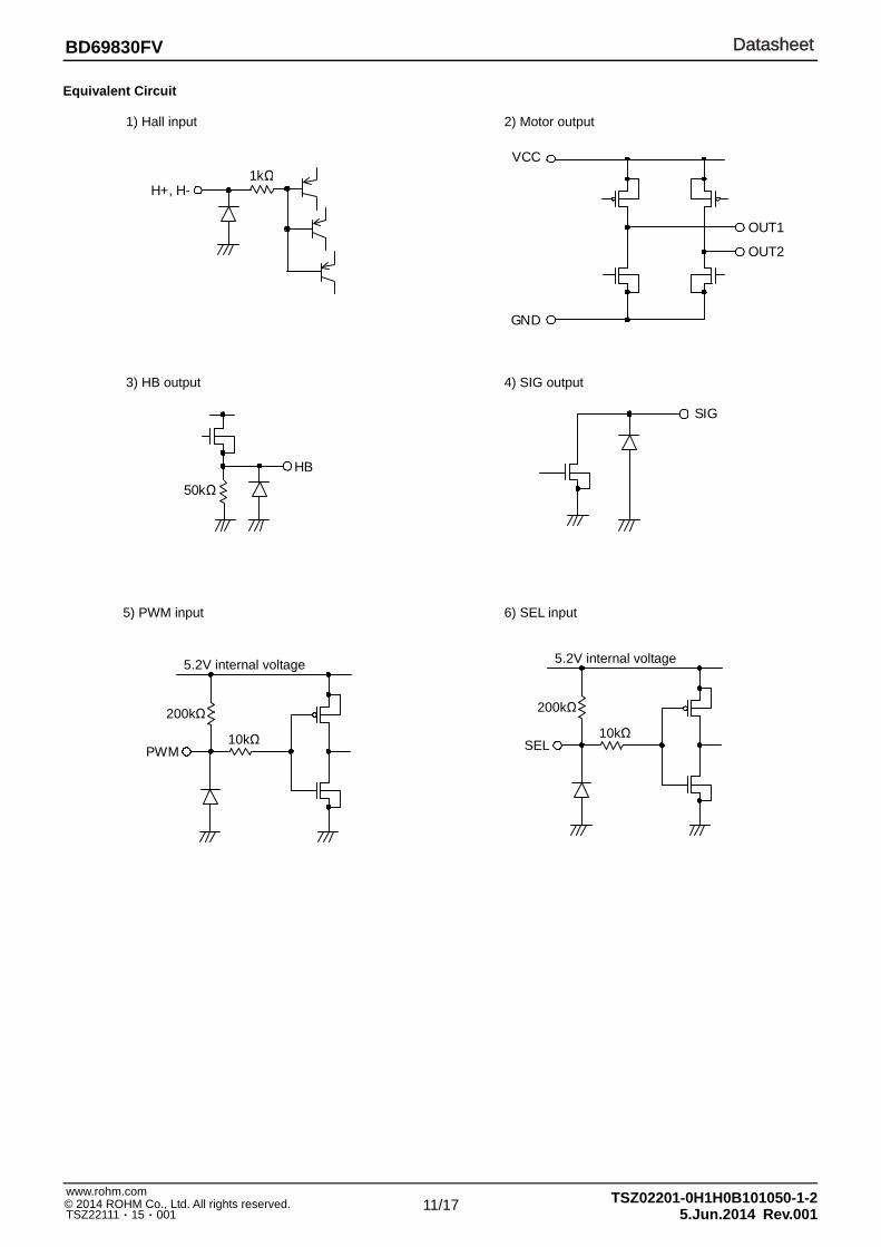
Equivalent Circuit
1) Hall input 2) Motor output 3) HB output 4) SIG output 5) PWM input 6) SEL input
OUT1
VCC
GND
OUT2
H+, H-
1kΩ
HB
50kΩ
SIG
PWM
200kΩ
10kΩ
5.2V internal voltage
SEL
200kΩ
10kΩ
5.2V internal voltage
DatasheetDatasheet
12/17 www.rohm.com © 2014 ROHM Co., Ltd. All rights reserved. TSZ22111・15・001
TSZ02201-0H1H0B101050-1-25.Jun.2014 Rev.001
BD69830FV
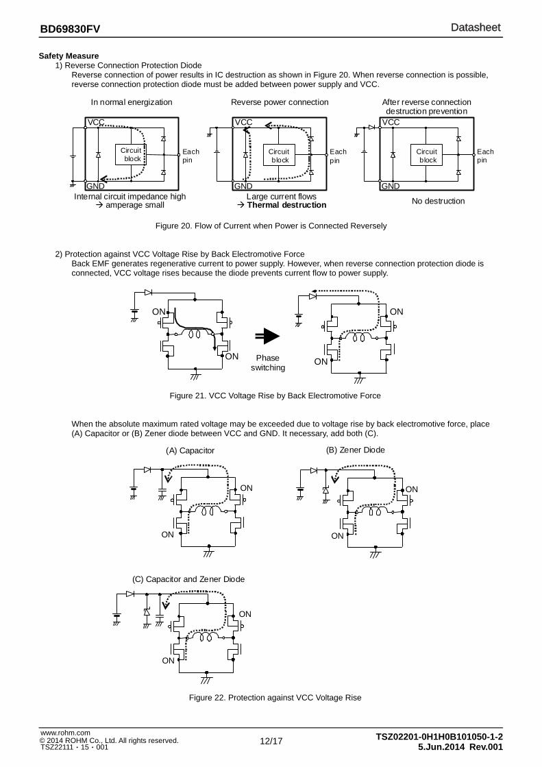
Safety Measure 1) Reverse Connection Protection Diode
Reverse connection of power results in IC destruction as shown in Figure 20. When reverse connection is possible, reverse connection protection diode must be added between power supply and VCC.
Figure 20. Flow of Current when Power is Connected Reversely
2) Protection against VCC Voltage Rise by Back Electromotive Force Back EMF generates regenerative current to power supply. However, when reverse connection protection diode is connected, VCC voltage rises because the diode prevents current flow to power supply.
Figure 21. VCC Voltage Rise by Back Electromotive Force
When the absolute maximum rated voltage may be exceeded due to voltage rise by back electromotive force, place (A) Capacitor or (B) Zener diode between VCC and GND. It necessary, add both (C).
Figure 22. Protection against VCC Voltage Rise
(A) Capacitor (B) Zener Diode
(C) Capacitor and Zener Diode
ON
ON ON
ON
ON
ON
Phase switching
ON
ON
ON
ON
VCC
GND
VCC
GND
VCC
GND Internal circuit impedance high
amperage small
Circuit block
Each pin
In normal energization
Large current flows Thermal destruction
Each pin
Circuit block
Reverse power connection
No destruction
Each pin
Circuit block
After reverse connection destruction prevention
DatasheetDatasheet
13/17 www.rohm.com © 2014 ROHM Co., Ltd. All rights reserved. TSZ22111・15・001
TSZ02201-0H1H0B101050-1-25.Jun.2014 Rev.001
BD69830FV
Pd(W)
1.0
0.870.8
0.6
0.4
0.2
0 25 50 75 105100 125 150 Ta(°C)
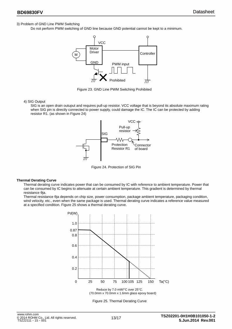
3) Problem of GND Line PWM Switching Do not perform PWM switching of GND line because GND potential cannot be kept to a minimum.
Figure 23. GND Line PWM Switching Prohibited
4) SIG Output SIG is an open drain outuput and requires pull-up resistor. VCC voltage that is beyond its absolute maximum rating when SIG pin is directly connected to power supply, could damage the IC. The IC can be protected by adding resistor R1. (as shown in Figure 24)
Figure 24. Protection of SIG Pin Thermal Derating Curve
Thermal derating curve indicates power that can be consumed by IC with reference to ambient temperature. Power that can be consumed by IC begins to attenuate at certain ambient temperature. This gradient is determined by thermal resistance θja. Thermal resistance θja depends on chip size, power consumption, package ambient temperature, packaging condition, wind velocity, etc., even when the same package is used. Thermal derating curve indicates a reference value measured at a specified condition. Figure 25 shows a thermal derating curve.
Reduce by 7.0 mW/°C over 25°C.
(70.0mm x 70.0mm x 1.6mm glass epoxy board)
Figure 25. Thermal Derating Curve
PWM input
Prohibited
VCCMotorDriver
GND
ControllerM
SIG
ProtectionResistor R1
Pull-up resistor
VCC
Connectorof board
DatasheetDatasheet
14/17 www.rohm.com © 2014 ROHM Co., Ltd. All rights reserved. TSZ22111・15・001
TSZ02201-0H1H0B101050-1-25.Jun.2014 Rev.001
BD69830FV
Operational Notes
1. Reverse Connection of Power Supply Connecting the power supply in reverse polarity can damage the IC. Take precautions against reverse polarity when connecting the power supply, such as mounting an external diode between the power supply and the IC’s power supply pins.
2. Power Supply Lines Design the PCB layout pattern to provide low impedance supply lines. Separate the ground and supply lines of the digital and analog blocks to prevent noise in the ground and supply lines of the digital block from affecting the analog block. Furthermore, connect a capacitor to ground at all power supply pins. Consider the effect of temperature and aging on the capacitance value when using electrolytic capacitors.
3. Ground Voltage Ensure that no pins are at a voltage below that of the ground pin at any time, even during transient condition. However, pins that drive inductive loads (e.g. motor driver outputs, DC-DC converter outputs) may inevitably go below ground due to back EMF or electromotive force. In such cases, the user should make sure that such voltages going below ground will not cause the IC and the system to malfunction by examining carefully all relevant factors and conditions such as motor characteristics, supply voltage, operating frequency and PCB wiring to name a few.
4. Ground Wiring Pattern
When using both small-signal and large-current ground traces, the two ground traces should be routed separately but connected to a single ground at the reference point of the application board to avoid fluctuations in the small-signal ground caused by large currents. Also ensure that the ground traces of external components do not cause variations on the ground voltage. The ground lines must be as short and thick as possible to reduce line impedance.
5. Thermal Consideration
Should by any chance the power dissipation rating be exceeded the rise in temperature of the chip may result in deterioration of the properties of the chip. The absolute maximum rating of the Pd stated in this specification is when the IC is mounted on a 70mm x 70mm x 1.6mm glass epoxy board. In case of exceeding this absolute maximum rating, increase the board size and copper area to prevent exceeding the Pd rating.
6. Recommended Operating Conditions
These conditions represent a range within which the expected characteristics of the IC can be approximately obtained. The electrical characteristics are guaranteed under the conditions of each parameter.
7. Inrush Current
When power is first supplied to the IC, it is possible that the internal logic may be unstable and inrush current may flow instantaneously due to the internal powering sequence and delays, especially if the IC has more than one power supply. Therefore, give special consideration to power coupling capacitance, power wiring, width of ground wiring, and routing of connections.
8. Operation Under Strong Electromagnetic Field
Operating the IC in the presence of a strong electromagnetic field may cause the IC to malfunction.
9. Testing on Application Boards When testing the IC on an application board, connecting a capacitor directly to a low-impedance output pin may subject the IC to stress. Always discharge capacitors completely after each process or step. The IC’s power supply should always be turned off completely before connecting or removing it from the test setup during the inspection process. To prevent damage from static discharge, ground the IC during assembly and use similar precautions during transport and storage.
10. Inter-pin Short and Mounting Errors Ensure that the direction and position are correct when mounting the IC on the PCB. Incorrect mounting may result in damaging the IC. Avoid nearby pins being shorted to each other especially to ground, power supply and output pin. Inter-pin shorts could be due to many reasons such as metal particles, water droplets (in very humid environment) and unintentional solder bridge deposited in between pins during assembly to name a few.
DatasheetDatasheet
15/17 www.rohm.com © 2014 ROHM Co., Ltd. All rights reserved. TSZ22111・15・001
TSZ02201-0H1H0B101050-1-25.Jun.2014 Rev.001
BD69830FV
Operational Notes – continued
11. Unused Input Pins Input pins of an IC are often connected to the gate of a MOS transistor. The gate has extremely high impedance and extremely low capacitance. If left unconnected, the electric field from the outside can easily charge it. The small charge acquired in this way is enough to produce a significant effect on the conduction through the transistor and cause unexpected operation of the IC. So unless otherwise specified, unused input pins should be connected to the power supply or ground line.
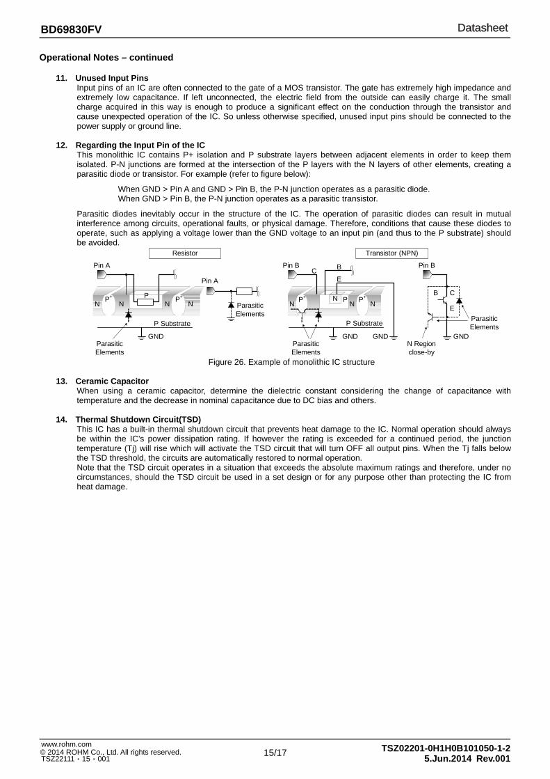
12. Regarding the Input Pin of the IC
This monolithic IC contains P+ isolation and P substrate layers between adjacent elements in order to keep them isolated. P-N junctions are formed at the intersection of the P layers with the N layers of other elements, creating a parasitic diode or transistor. For example (refer to figure below):
When GND > Pin A and GND > Pin B, the P-N junction operates as a parasitic diode. When GND > Pin B, the P-N junction operates as a parasitic transistor.
Parasitic diodes inevitably occur in the structure of the IC. The operation of parasitic diodes can result in mutual interference among circuits, operational faults, or physical damage. Therefore, conditions that cause these diodes to operate, such as applying a voltage lower than the GND voltage to an input pin (and thus to the P substrate) should be avoided.
Figure 26. Example of monolithic IC structure
13. Ceramic Capacitor When using a ceramic capacitor, determine the dielectric constant considering the change of capacitance with temperature and the decrease in nominal capacitance due to DC bias and others.
14. Thermal Shutdown Circuit(TSD) This IC has a built-in thermal shutdown circuit that prevents heat damage to the IC. Normal operation should always be within the IC’s power dissipation rating. If however the rating is exceeded for a continued period, the junction temperature (Tj) will rise which will activate the TSD circuit that will turn OFF all output pins. When the Tj falls below the TSD threshold, the circuits are automatically restored to normal operation. Note that the TSD circuit operates in a situation that exceeds the absolute maximum ratings and therefore, under no circumstances, should the TSD circuit be used in a set design or for any purpose other than protecting the IC from heat damage.
N NP+ PN NP+
P Substrate
GND
N P+
N NP+N P
P Substrate
GND GND
Parasitic Elements
Pin A
Pin A
Pin B Pin B
B C
EParasitic Elements
GNDParasitic Elements
C B
E
Transistor (NPN)Resistor
N Regionclose-by
Parasitic Elements
DatasheetDatasheet
16/17 www.rohm.com © 2014 ROHM Co., Ltd. All rights reserved. TSZ22111・15・001
TSZ02201-0H1H0B101050-1-25.Jun.2014 Rev.001
BD69830FV
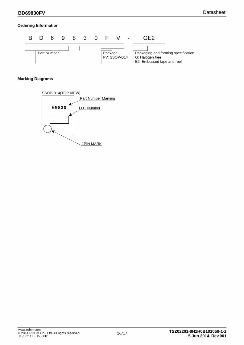
Ordering Information
B D 6 9 8 3 0 F V - GE2
Part Number
Package FV: SSOP-B14
Packaging and forming specification G: Halogen free E2: Embossed tape and reel
Marking Diagrams
SSOP-B14(TOP VIEW)
69830
Part Number Marking
LOT Number
1PIN MARK
DatasheetDatasheet
17/17 www.rohm.com © 2014 ROHM Co., Ltd. All rights reserved. TSZ22111・15・001
TSZ02201-0H1H0B101050-1-25.Jun.2014 Rev.001
BD69830FV
Physical Dimension, Tape and Reel Information Package Name SSOP-B14
∗ Order quantity needs to be multiple of the minimum quantity.
<Tape and Reel information>
Embossed carrier tapeTape
Quantity
Direction of feed
The direction is the 1pin of product is at the upper left when you hold reel on the left hand and you pull out the tape on the right hand
2500pcs
E2
( )
Direction of feed
Reel1pin
DatasheetDatasheet
Notice – GE Rev.002© 2013 ROHM Co., Ltd. All rights reserved.
Notice Precaution on using ROHM Products
1. Our Products are designed and manufactured for application in ordinary electronic equipments (such as AV equipment, OA equipment, telecommunication equipment, home electronic appliances, amusement equipment, etc.). If you intend to use our Products in devices requiring extremely high reliability (such as medical equipment (Note 1), transport equipment, traffic equipment, aircraft/spacecraft, nuclear power controllers, fuel controllers, car equipment including car accessories, safety devices, etc.) and whose malfunction or failure may cause loss of human life, bodily injury or serious damage to property (“Specific Applications”), please consult with the ROHM sales representative in advance. Unless otherwise agreed in writing by ROHM in advance, ROHM shall not be in any way responsible or liable for any damages, expenses or losses incurred by you or third parties arising from the use of any ROHM’s Products for Specific Applications.
(Note1) Medical Equipment Classification of the Specific Applications JAPAN USA EU CHINA
CLASSⅢ CLASSⅢ
CLASSⅡb CLASSⅢ
CLASSⅣ CLASSⅢ
2. ROHM designs and manufactures its Products subject to strict quality control system. However, semiconductor products can fail or malfunction at a certain rate. Please be sure to implement, at your own responsibilities, adequate safety measures including but not limited to fail-safe design against the physical injury, damage to any property, which a failure or malfunction of our Products may cause. The following are examples of safety measures:
[a] Installation of protection circuits or other protective devices to improve system safety [b] Installation of redundant circuits to reduce the impact of single or multiple circuit failure
3. Our Products are designed and manufactured for use under standard conditions and not under any special or extraordinary environments or conditions, as exemplified below. Accordingly, ROHM shall not be in any way responsible or liable for any damages, expenses or losses arising from the use of any ROHM’s Products under any special or extraordinary environments or conditions. If you intend to use our Products under any special or extraordinary environments or conditions (as exemplified below), your independent verification and confirmation of product performance, reliability, etc, prior to use, must be necessary:
[a] Use of our Products in any types of liquid, including water, oils, chemicals, and organic solvents [b] Use of our Products outdoors or in places where the Products are exposed to direct sunlight or dust [c] Use of our Products in places where the Products are exposed to sea wind or corrosive gases, including Cl2,
H2S, NH3, SO2, and NO2 [d] Use of our Products in places where the Products are exposed to static electricity or electromagnetic waves [e] Use of our Products in proximity to heat-producing components, plastic cords, or other flammable items [f] Sealing or coating our Products with resin or other coating materials [g] Use of our Products without cleaning residue of flux (even if you use no-clean type fluxes, cleaning residue of
flux is recommended); or Washing our Products by using water or water-soluble cleaning agents for cleaning residue after soldering
[h] Use of the Products in places subject to dew condensation
4. The Products are not subject to radiation-proof design. 5. Please verify and confirm characteristics of the final or mounted products in using the Products. 6. In particular, if a transient load (a large amount of load applied in a short period of time, such as pulse. is applied,
confirmation of performance characteristics after on-board mounting is strongly recommended. Avoid applying power exceeding normal rated power; exceeding the power rating under steady-state loading condition may negatively affect product performance and reliability.
7. De-rate Power Dissipation (Pd) depending on Ambient temperature (Ta). When used in sealed area, confirm the actual
ambient temperature. 8. Confirm that operation temperature is within the specified range described in the product specification. 9. ROHM shall not be in any way responsible or liable for failure induced under deviant condition from what is defined in
this document.
Precaution for Mounting / Circuit board design 1. When a highly active halogenous (chlorine, bromine, etc.) flux is used, the residue of flux may negatively affect product
performance and reliability. 2. In principle, the reflow soldering method must be used; if flow soldering method is preferred, please consult with the
ROHM representative in advance. For details, please refer to ROHM Mounting specification

DatasheetDatasheet
Notice – GE Rev.002© 2013 ROHM Co., Ltd. All rights reserved.
Precautions Regarding Application Examples and External Circuits 1. If change is made to the constant of an external circuit, please allow a sufficient margin considering variations of the
characteristics of the Products and external components, including transient characteristics, as well as static characteristics.
2. You agree that application notes, reference designs, and associated data and information contained in this document
are presented only as guidance for Products use. Therefore, in case you use such information, you are solely responsible for it and you must exercise your own independent verification and judgment in the use of such information contained in this document. ROHM shall not be in any way responsible or liable for any damages, expenses or losses incurred by you or third parties arising from the use of such information.
Precaution for Electrostatic
This Product is electrostatic sensitive product, which may be damaged due to electrostatic discharge. Please take proper caution in your manufacturing process and storage so that voltage exceeding the Products maximum rating will not be applied to Products. Please take special care under dry condition (e.g. Grounding of human body / equipment / solder iron, isolation from charged objects, setting of Ionizer, friction prevention and temperature / humidity control).
Precaution for Storage / Transportation 1. Product performance and soldered connections may deteriorate if the Products are stored in the places where:
[a] the Products are exposed to sea winds or corrosive gases, including Cl2, H2S, NH3, SO2, and NO2 [b] the temperature or humidity exceeds those recommended by ROHM [c] the Products are exposed to direct sunshine or condensation [d] the Products are exposed to high Electrostatic
2. Even under ROHM recommended storage condition, solderability of products out of recommended storage time period may be degraded. It is strongly recommended to confirm solderability before using Products of which storage time is exceeding the recommended storage time period.
3. Store / transport cartons in the correct direction, which is indicated on a carton with a symbol. Otherwise bent leads
may occur due to excessive stress applied when dropping of a carton. 4. Use Products within the specified time after opening a humidity barrier bag. Baking is required before using Products of
which storage time is exceeding the recommended storage time period.
Precaution for Product Label QR code printed on ROHM Products label is for ROHM’s internal use only.
Precaution for Disposition When disposing Products please dispose them properly using an authorized industry waste company.
Precaution for Foreign Exchange and Foreign Trade act Since our Products might fall under controlled goods prescribed by the applicable foreign exchange and foreign trade act, please consult with ROHM representative in case of export.
Precaution Regarding Intellectual Property Rights 1. All information and data including but not limited to application example contained in this document is for reference
only. ROHM does not warrant that foregoing information or data will not infringe any intellectual property rights or any other rights of any third party regarding such information or data. ROHM shall not be in any way responsible or liable for infringement of any intellectual property rights or other damages arising from use of such information or data.:
2. No license, expressly or implied, is granted hereby under any intellectual property rights or other rights of ROHM or any
third parties with respect to the information contained in this document.
Other Precaution 1. This document may not be reprinted or reproduced, in whole or in part, without prior written consent of ROHM. 2. The Products may not be disassembled, converted, modified, reproduced or otherwise changed without prior written
consent of ROHM. 3. In no event shall you use in any way whatsoever the Products and the related technical information contained in the
Products or this document for any military purposes, including but not limited to, the development of mass-destruction weapons.
4. The proper names of companies or products described in this document are trademarks or registered trademarks of
ROHM, its affiliated companies or third parties.
DatasheetDatasheet
Notice – WE Rev.001© 2014 ROHM Co., Ltd. All rights reserved.
General Precaution 1. Before you use our Pro ducts, you are requested to care fully read this document and fully understand its contents.
ROHM shall n ot be in an y way responsible or liabl e for fa ilure, malfunction or acci dent arising from the use of a ny ROHM’s Products against warning, caution or note contained in this document.
2. All information contained in this docume nt is current as of the issuing date and subj ect to change without any prior
notice. Before purchasing or using ROHM’s Products, please confirm the la test information with a ROHM sale s representative.
3. The information contained in this doc ument is provi ded on an “as is” basis and ROHM does not warrant that all
information contained in this document is accurate an d/or error-free. ROHM shall not be in an y way responsible or liable for any damages, expenses or losses incurred by you or third parties resulting from inaccuracy or errors of or concerning such information.