Embed Size (px)
Citation preview
○Product structure:Silicon monolithic integrated circuit ○This product has no designed protection against radioactive rays
1/31 © 2015 ROHM Co., Ltd. All rights reserved. www.rohm.com
TSZ22111・14・001
TSZ02201-0H1H0B101220-1-2
13.Jul.2015 Rev.002
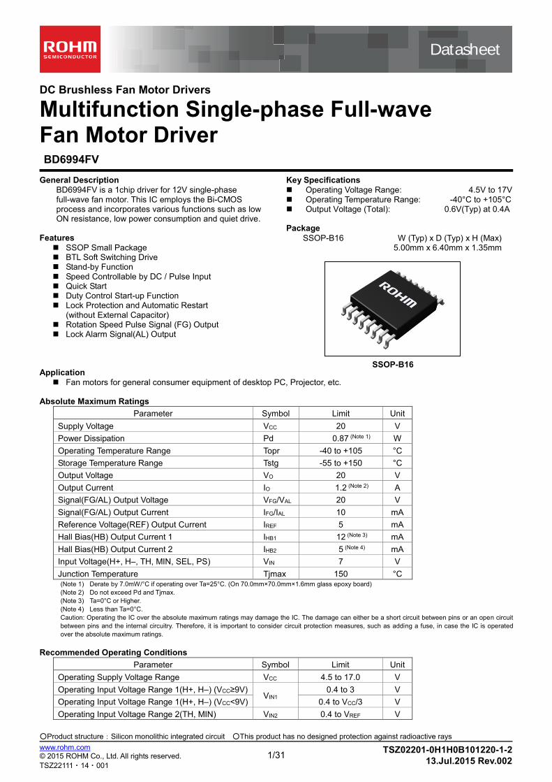
DC Brushless Fan Motor Drivers
Multifunction Single-phase Full-wave Fan Motor Driver BD6994FV
General Description
BD6994FV is a 1chip driver for 12V single-phase full-wave fan motor. This IC employs the Bi-CMOS process and incorporates various functions such as low ON resistance, low power consumption and quiet drive.
Features
SSOP Small Package BTL Soft Switching Drive Stand-by Function Speed Controllable by DC / Pulse Input Quick Start Duty Control Start-up Function Lock Protection and Automatic Restart
(without External Capacitor) Rotation Speed Pulse Signal (FG) Output Lock Alarm Signal(AL) Output
Key Specifications
Operating Voltage Range: 4.5V to 17V Operating Temperature Range: -40°C to +105°C Output Voltage (Total): 0.6V(Typ) at 0.4A Package
SSOP-B16 W (Typ) x D (Typ) x H (Max) 5.00mm x 6.40mm x 1.35mm
Application
Fan motors for general consumer equipment of desktop PC, Projector, etc. Absolute Maximum Ratings
Parameter Symbol Limit Unit
Supply Voltage VCC 20 V
Power Dissipation Pd 0.87 (Note 1) W
Operating Temperature Range Topr -40 to +105 °C
Storage Temperature Range Tstg -55 to +150 °C
Output Voltage VO 20 V
Output Current IO 1.2 (Note 2) A
Signal(FG/AL) Output Voltage VFG/VAL 20 V
Signal(FG/AL) Output Current IFG/IAL 10 mA
Reference Voltage(REF) Output Current IREF 5 mA
Hall Bias(HB) Output Current 1 IHB1 12 (Note 3) mA
Hall Bias(HB) Output Current 2 IHB2 5 (Note 4) mA
Input Voltage(H+, H–, TH, MIN, SEL, PS) VIN 7 V
Junction Temperature Tjmax 150 °C (Note 1) Derate by 7.0mW/°C if operating over Ta=25°C. (On 70.0mm×70.0mm×1.6mm glass epoxy board)
(Note 2) Do not exceed Pd and Tjmax.
(Note 3) Ta=0°C or Higher.
(Note 4) Less than Ta=0°C.
Caution: Operating the IC over the absolute maximum ratings may damage the IC. The damage can either be a short circuit between pins or an open circuit
between pins and the internal circuitry. Therefore, it is important to consider circuit protection measures, such as adding a fuse, in case the IC is operated
over the absolute maximum ratings.
Recommended Operating Conditions
Parameter Symbol Limit Unit
Operating Supply Voltage Range VCC 4.5 to 17.0 V
Operating Input Voltage Range 1(H+, H–) (VCC≥9V) VIN1
0.4 to 3 V
Operating Input Voltage Range 1(H+, H–) (VCC<9V) 0.4 to VCC/3 V
Operating Input Voltage Range 2(TH, MIN) VIN2 0.4 to VREF V
SSOP-B16
Datasheet
2/31
BD6994FV
© 2015 ROHM Co., Ltd. All rights reserved.
www.rohm.com
TSZ22111・15・001
TSZ02201-0H1H0B101220-1-2 13.Jul.2015 Rev.002
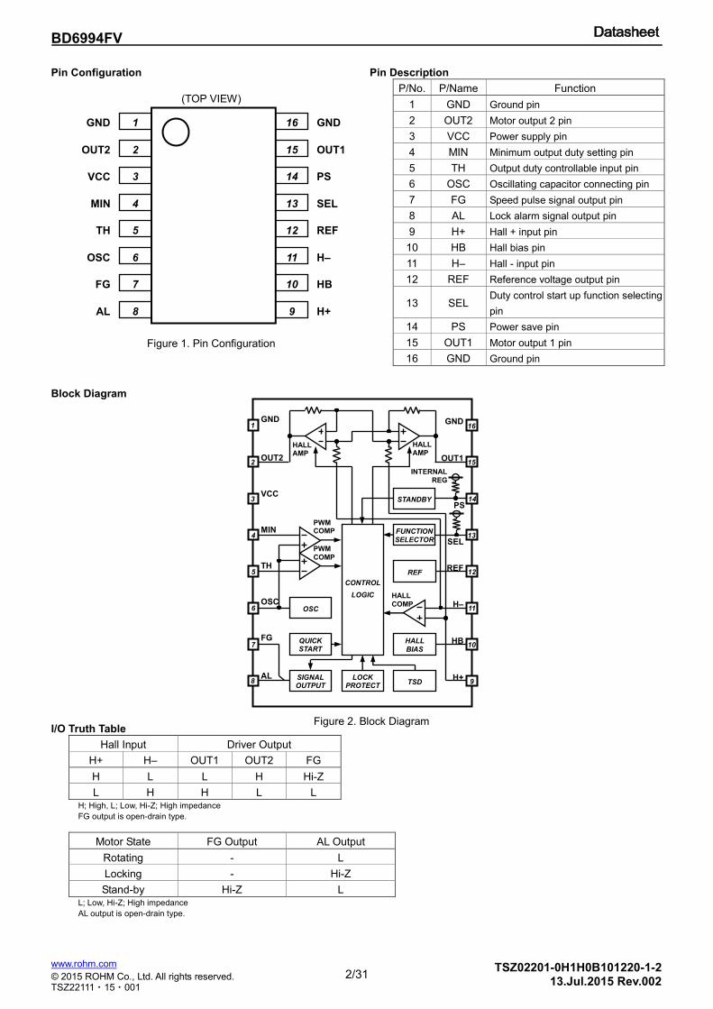
Pin Configuration
Pin Description
P/No. P/Name Function
1 GND Ground pin
2 OUT2 Motor output 2 pin
3 VCC Power supply pin
4 MIN Minimum output duty setting pin
5 TH Output duty controllable input pin
6 OSC Oscillating capacitor connecting pin
7 FG Speed pulse signal output pin
8 AL Lock alarm signal output pin
9 H+ Hall + input pin
10 HB Hall bias pin
11 H– Hall - input pin
12 REF Reference voltage output pin
13 SEL Duty control start up function selecting
pin
14 PS Power save pin
15 OUT1 Motor output 1 pin
16 GND Ground pin
Block Diagram
I/O Truth Table
Hall Input Driver Output
H+ H– OUT1 OUT2 FG
H L L H Hi-Z
L H H L L H; High, L; Low, Hi-Z; High impedance
FG output is open-drain type.
Motor State FG Output AL Output
Rotating - L
Locking - Hi-Z
Stand-by Hi-Z L L; Low, Hi-Z; High impedance
AL output is open-drain type.
VCC
cc
TH
PS
FG
SEL
OUT1
GND
HB
OSC
OUT2
H–
GND
MIN
AL
1
2
3
4
5
6
7
15
H+
REF
16
8
14
13
12
11
9
10
HALL
BIAS
Figure 2. Block Diagram
Figure 1. Pin Configuration
(TOP VIEW)
HALL AMP
HALL
COMP
1
2
3
4
5
6
7
8 9
10
11
12
13
15
16
PWM
COMP
PWM COMP
INTERNAL
REG
14
OSC
REF
HALL
BIAS
SIGNAL OUTPUT
TSD LOCK
PROTECT
QUICK START
CONTROL
LOGIC
FUNCTION
SELECTOR
HALL AMP
STANDBY
MIN
TH
FG
OSC
VCC
OUT2
GND
AL
OUT1
HB
H–
REF
SEL
GND
H+
PS
3/31
BD6994FV
© 2015 ROHM Co., Ltd. All rights reserved.
www.rohm.com
TSZ22111・15・001
TSZ02201-0H1H0B101220-1-2 13.Jul.2015 Rev.002
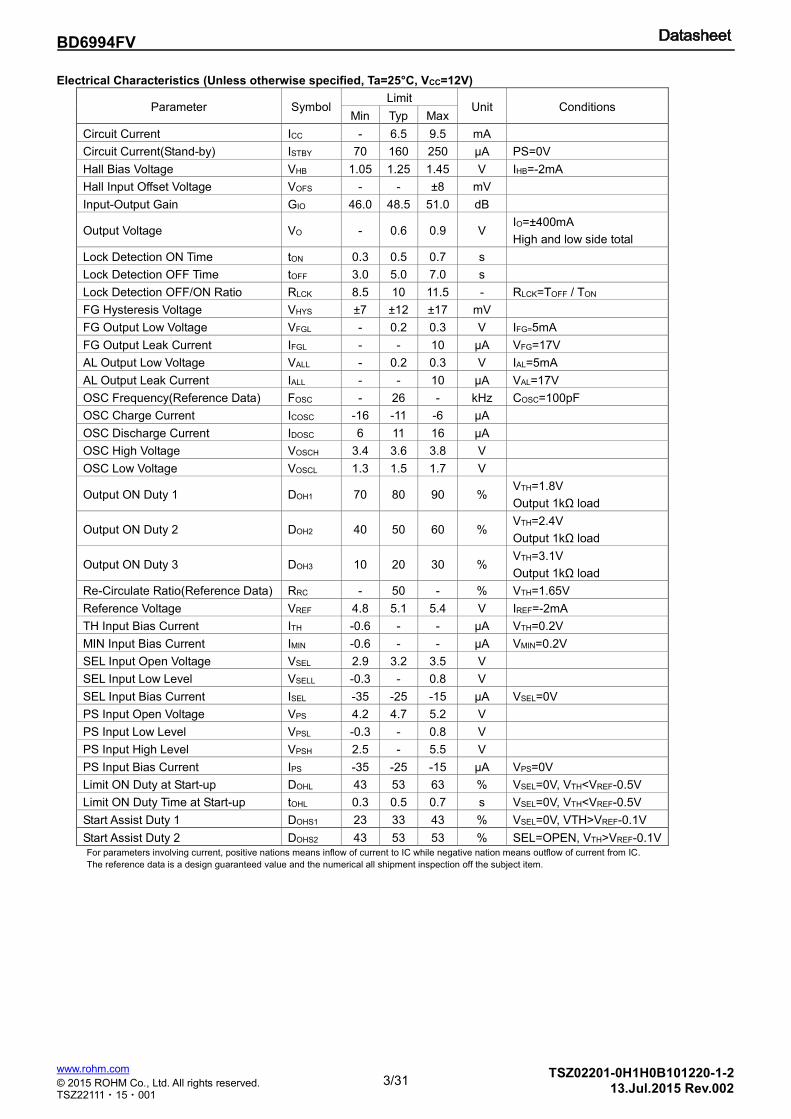
Electrical Characteristics (Unless otherwise specified, Ta=25°C, VCC=12V)
Parameter Symbol Limit
Unit Conditions Min Typ Max
Circuit Current ICC - 6.5 9.5 mA
Circuit Current(Stand-by) ISTBY 70 160 250 μA PS=0V
Hall Bias Voltage VHB 1.05 1.25 1.45 V IHB=-2mA
Hall Input Offset Voltage VOFS - - ±8 mV
Input-Output Gain GIO 46.0 48.5 51.0 dB
Output Voltage VO - 0.6 0.9 V IO=±400mA
High and low side total
Lock Detection ON Time tON 0.3 0.5 0.7 s
Lock Detection OFF Time tOFF 3.0 5.0 7.0 s
Lock Detection OFF/ON Ratio RLCK 8.5 10 11.5 - RLCK=TOFF / TON
FG Hysteresis Voltage VHYS ±7 ±12 ±17 mV
FG Output Low Voltage VFGL - 0.2 0.3 V IFG=5mA
FG Output Leak Current IFGL - - 10 μA VFG=17V
AL Output Low Voltage VALL - 0.2 0.3 V IAL=5mA
AL Output Leak Current IALL - - 10 μA VAL=17V
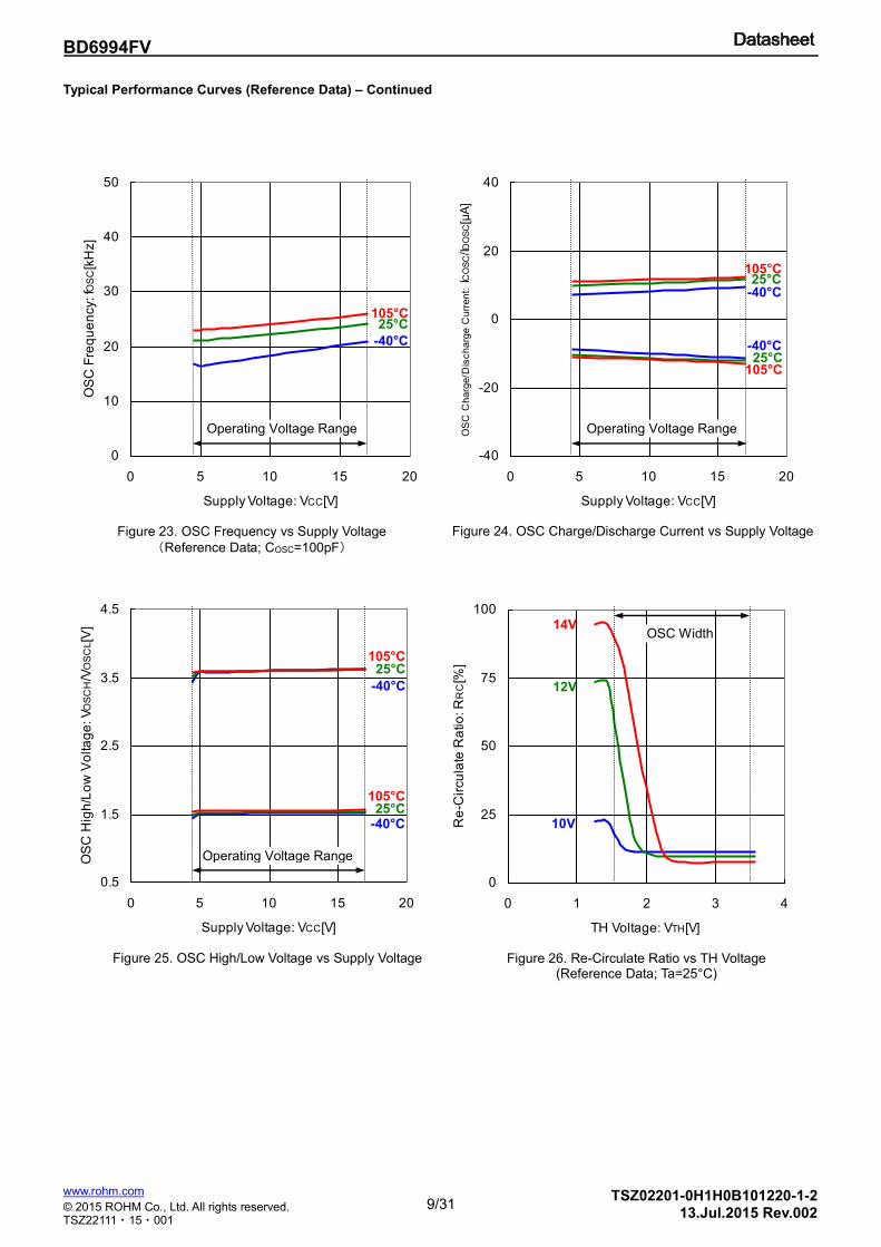
OSC Frequency(Reference Data) FOSC - 26 - kHz COSC=100pF
OSC Charge Current ICOSC -16 -11 -6 μA
OSC Discharge Current IDOSC 6 11 16 μA
OSC High Voltage VOSCH 3.4 3.6 3.8 V
OSC Low Voltage VOSCL 1.3 1.5 1.7 V
Output ON Duty 1 DOH1 70 80 90 % VTH=1.8V
Output 1kΩ load
Output ON Duty 2 DOH2 40 50 60 % VTH=2.4V
Output 1kΩ load
Output ON Duty 3 DOH3 10 20 30 % VTH=3.1V
Output 1kΩ load
Re-Circulate Ratio(Reference Data) RRC - 50 - % VTH=1.65V
Reference Voltage VREF 4.8 5.1 5.4 V IREF=-2mA
TH Input Bias Current ITH -0.6 - - μA VTH=0.2V
MIN Input Bias Current IMIN -0.6 - - μA VMIN=0.2V
SEL Input Open Voltage VSEL 2.9 3.2 3.5 V
SEL Input Low Level VSELL -0.3 - 0.8 V
SEL Input Bias Current ISEL -35 -25 -15 μA VSEL=0V
PS Input Open Voltage VPS 4.2 4.7 5.2 V
PS Input Low Level VPSL -0.3 - 0.8 V
PS Input High Level VPSH 2.5 - 5.5 V
PS Input Bias Current IPS -35 -25 -15 μA VPS=0V
Limit ON Duty at Start-up DOHL 43 53 63 % VSEL=0V, VTH<VREF-0.5V
Limit ON Duty Time at Start-up tOHL 0.3 0.5 0.7 s VSEL=0V, VTH<VREF-0.5V
Start Assist Duty 1 DOHS1 23 33 43 % VSEL=0V, VTH>VREF-0.1V
Start Assist Duty 2 DOHS2 43 53 53 % SEL=OPEN, VTH>VREF-0.1V For parameters involving current, positive nations means inflow of current to IC while negative nation means outflow of current from IC.
The reference data is a design guaranteed value and the numerical all shipment inspection off the subject item.
4/31
BD6994FV
© 2015 ROHM Co., Ltd. All rights reserved.
www.rohm.com
TSZ22111・15・001
TSZ02201-0H1H0B101220-1-2 13.Jul.2015 Rev.002
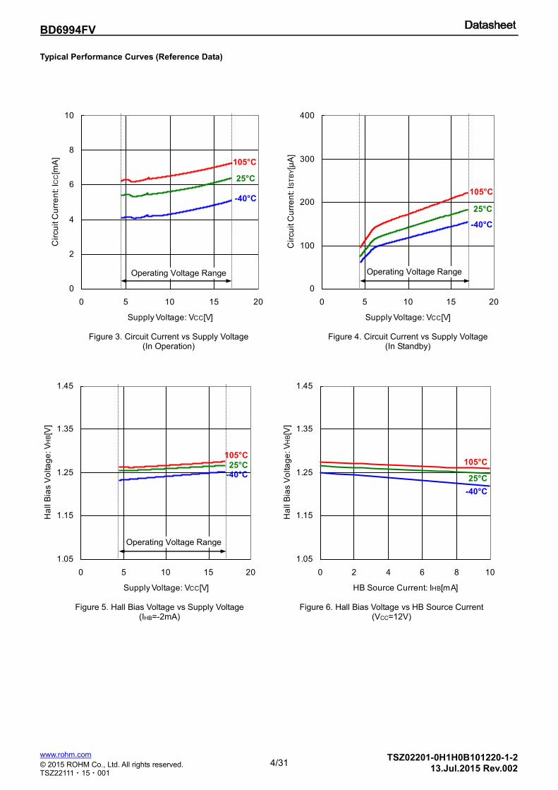
Typical Performance Curves (Reference Data)
Figure 3. Circuit Current vs Supply Voltage (In Operation)
Figure 4. Circuit Current vs Supply Voltage (In Standby)
Figure 5. Hall Bias Voltage vs Supply Voltage (IHB=-2mA)
0
2
4
6
8
10
0 5 10 15 20
Supply Voltage: VCC[V]
Cir
cu
it C
urr
en
t: I
CC
[mA
]
-40°C
105°C
25°C
Operating Voltage Range
0
100
200
300
400
0 5 10 15 20
Supply Voltage: VCC[V]
Cir
cu
it C
urr
en
t: I
ST
BY[μ
A]
-40°C
105°C
25°C
Operating Voltage Range
Figure 6. Hall Bias Voltage vs HB Source Current (VCC=12V)
1.05
1.15
1.25
1.35
1.45
0 5 10 15 20
Supply Voltage: VCC[V]
Ha
ll B
ias V
olta
ge
: V
HB[V
]
-40°C
105°C
25°C
1.05
1.15
1.25
1.35
1.45
0 2 4 6 8 10
HB Source Current: IHB[mA]
Ha
ll B
ias V
olta
ge
: V
HB[V
]
-40°C
105°C
25°C
Operating Voltage Range
5/31
BD6994FV
© 2015 ROHM Co., Ltd. All rights reserved.
www.rohm.com
TSZ22111・15・001
TSZ02201-0H1H0B101220-1-2 13.Jul.2015 Rev.002
Typical Performance Curves (Reference Data) - Continued
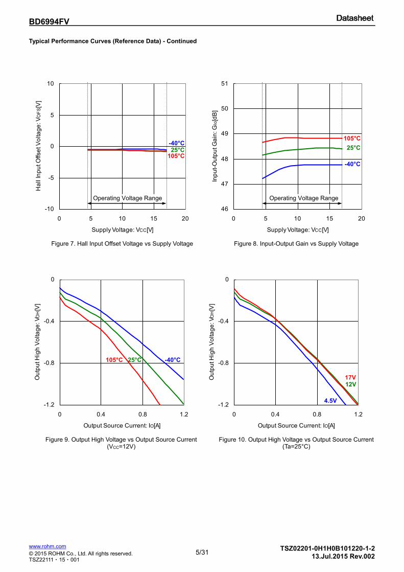
Figure 9. Output High Voltage vs Output Source Current (VCC=12V)
Figure 8. Input-Output Gain vs Supply Voltage Figure 7. Hall Input Offset Voltage vs Supply Voltage
-10
-5
0
5
10
0 5 10 15 20
Supply Voltage: VCC[V]
Ha
ll In
pu
t O
ffse
t V
olta
ge
: V
OF
S[V
]
-40°C
105°C 25°C
-1.2
-0.8
-0.4
0
0 0.4 0.8 1.2
Output Source Current: IO[A]
Ou
tpu
t H
igh
Vo
lta
ge
: V
OH
[V]
-40°C 105°C 25°C
-1.2
-0.8
-0.4
0
0 0.4 0.8 1.2
Output Source Current: IO[A]
Ou
tpu
t H
igh
Vo
lta
ge
: V
OH
[V]
4.5V
17V 12V
46
47
48
49
50
51
0 5 10 15 20
Supply Voltage: VCC[V]
Inp
ut-
Ou
tpu
t G
ain
: G
Io[d
B]
-40°C
105°C
25°C
Operating Voltage Range Operating Voltage Range
Figure 10. Output High Voltage vs Output Source Current (Ta=25°C)
6/31
BD6994FV
© 2015 ROHM Co., Ltd. All rights reserved.
www.rohm.com
TSZ22111・15・001
TSZ02201-0H1H0B101220-1-2 13.Jul.2015 Rev.002
Typical Performance Curves (Reference Data) - Continued
0.3
0.4
0.5
0.6
0.7
0 5 10 15 20
Supply Voltage: VCC[V]
Lo
ck D
ete
ctio
n O
N T
ime
: tO
N[s
]
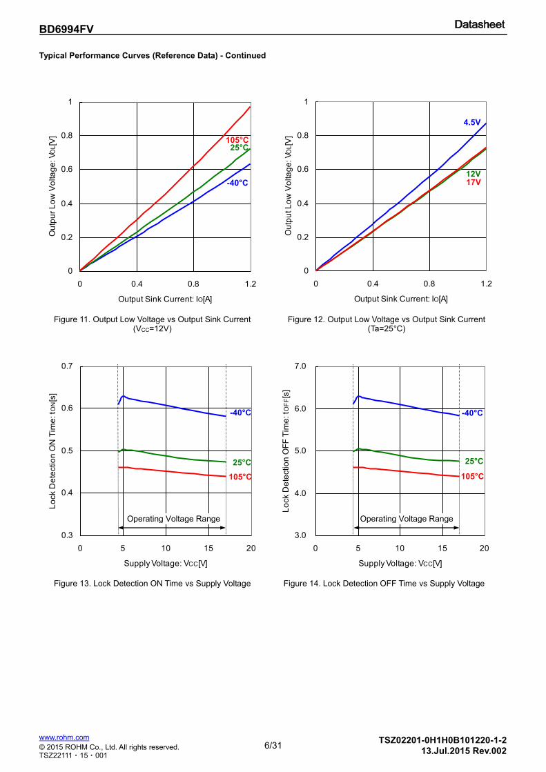
Figure 14. Lock Detection OFF Time vs Supply Voltage
Figure 11. Output Low Voltage vs Output Sink Current (VCC=12V)
Figure 12. Output Low Voltage vs Output Sink Current (Ta=25°C)
Figure 13. Lock Detection ON Time vs Supply Voltage
3.0
4.0
5.0
6.0
7.0
0 5 10 15 20
Supply Voltage: VCC[V]
Lo
ck D
ete
ctio
n O
FF
Tim
e: tO
FF[s
]
-40°C
105°C
25°C
0
0.2
0.4
0.6
0.8
1
0 0.4 0.8 1.2
Output Sink Current: IO[A]
Ou
tpu
r L
ow
Vo
lta
ge
: V
OL[V
]
-40°C
105°C 25°C
0
0.2
0.4
0.6
0.8
1
0 0.4 0.8 1.2
Output Sink Current: IO[A]
Ou
tpu
t L
ow
Vo
lta
ge
: V
OL[V
]
4.5V
17V 12V
-40°C
105°C
25°C
Operating Voltage Range Operating Voltage Range
7/31
BD6994FV
© 2015 ROHM Co., Ltd. All rights reserved.
www.rohm.com
TSZ22111・15・001
TSZ02201-0H1H0B101220-1-2 13.Jul.2015 Rev.002
Typical Performance Curves (Reference Data) - Continued
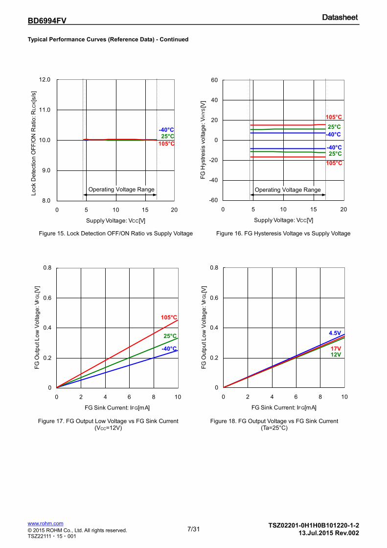
-60
-40
-20
0
20
40
60
0 5 10 15 20
Supply Voltage: VCC[V]
FG
Hystr
esis
vo
lta
ge
: V
HY
S[V
]
0
0.2
0.4
0.6
0.8
0 2 4 6 8 10
FG Sink Current: IFG[mA]
FG
Ou
tpu
t L
ow
Vo
lta
ge
: V
FG
L[V
]
4.5V
17V 12V
Figure 18. FG Output Voltage vs FG Sink Current (Ta=25°C)
0
0.2
0.4
0.6
0.8
0 2 4 6 8 10
FG Sink Current: IFG[mA]
FG
Ou
tpu
t L
ow
Vo
lta
ge
: V
FG
L[V
]
-40°C
105°C
25°C
Figure 17. FG Output Low Voltage vs FG Sink Current (VCC=12V)
Figure 16. FG Hysteresis Voltage vs Supply Voltage Figure 15. Lock Detection OFF/ON Ratio vs Supply Voltage
8.0
9.0
10.0
11.0
12.0
0 5 10 15 20
Supply Voltage: VCC[V]
Lo
ck D
ete
ctio
n O
FF
/ON
Ra
tio
: R
LC
K[s
/s]
-40°C
105°C
25°C -40°C
105°C
25°C
105°C
25°C -40°C
Operating Voltage Range Operating Voltage Range

8/31
BD6994FV
© 2015 ROHM Co., Ltd. All rights reserved.
www.rohm.com
TSZ22111・15・001
TSZ02201-0H1H0B101220-1-2 13.Jul.2015 Rev.002
Typical Performance Curves (Reference Data) - Continued
-0.2
0
0.2
0.4
0.6
0.8
0 5 10 15 20
AL Voltage: VAL[V]
AL
Ou
tpu
t L
ea
k C
urr
en
t: IA
LL[μ
A]
0
0.2
0.4
0.6
0.8
0 2 4 6 8 10
AL Sink Current: IAL[mA]
AL
Ou
tpu
t L
ow
Vo
lta
ge
: VA
LL[V
]
-40°C
105°C
25°C
Figure 22. AL Output Leak Current vs AL Voltage
4.5V
17V 12V
Figure 21. AL Output Low Voltage vs AL Sink Current (Ta=25°C)
回路電流 vs 電源電圧
0
0.2
0.4
0.6
0.8
0 2 4 6 8 10
AL Sink Current: IAL[mA]
AL
Ou
tpu
t L
ow
Vo
lta
ge
: VA
LL[V
]
-40°C
105°C
25°C
Figure 20. AL Output Low Voltage vs AL Sink Current (VCC=12V)
-2
0
2
4
6
8
0 5 10 15 20
FG Voltage: VFG[V]
FG
Ou
tpu
t L
ea
k C
urr
en
t: I
FG
L[μ
A]
Operating Voltage Range -40°C
105°C 25°C
Figure 19. FG Output Leak Current vs FG Voltage
Operating Voltage Range
9/31
BD6994FV
© 2015 ROHM Co., Ltd. All rights reserved.
www.rohm.com
TSZ22111・15・001
TSZ02201-0H1H0B101220-1-2 13.Jul.2015 Rev.002
Typical Performance Curves (Reference Data) – Continued
0.5
1.5
2.5
3.5
4.5
0 5 10 15 20
Supply Voltage: VCC[V]
OS
C H
igh
/Lo
w V
olta
ge
: V
OS
CH
/VO
SC
L[V
]
105°C 25°C
-40°C
0
25
50
75
100
0 1 2 3 4
TH Voltage: VTH[V]
Re
-Cir
cu
late
Ra
tio
: R
RC
[%]
10V
14V
12V -40°C
105°C 25°C
Figure 26. Re-Circulate Ratio vs TH Voltage (Reference Data; Ta=25°C)
pF)
Figure 23. OSC Frequency vs Supply Voltage
(Reference Data; COSC=100pF)
-40
-20
0
20
40
0 5 10 15 20
Supply Voltage: VCC[V]
OS
C C
harg
e/D
isch
arg
e C
urr
en
t: I
CO
SC/ID
OS
C[μ
A]
Operating Voltage Range
-40°C
105°C 25°C
Figure 24. OSC Charge/Discharge Current vs Supply Voltage
105°C 25°C
-40°C
Figure 25. OSC High/Low Voltage vs Supply Voltage
0
10
20
30
40
50
0 5 10 15 20
Supply Voltage: VCC[V]
OS
C F
req
ue
ncy: fO
SC
[kH
z]
-40°C
105°C 25°C
OSC Width
Operating Voltage Range
Operating Voltage Range
10/31
BD6994FV
© 2015 ROHM Co., Ltd. All rights reserved.
www.rohm.com
TSZ22111・15・001
TSZ02201-0H1H0B101220-1-2 13.Jul.2015 Rev.002
Typical Performance Curves (Reference Data) – Continued
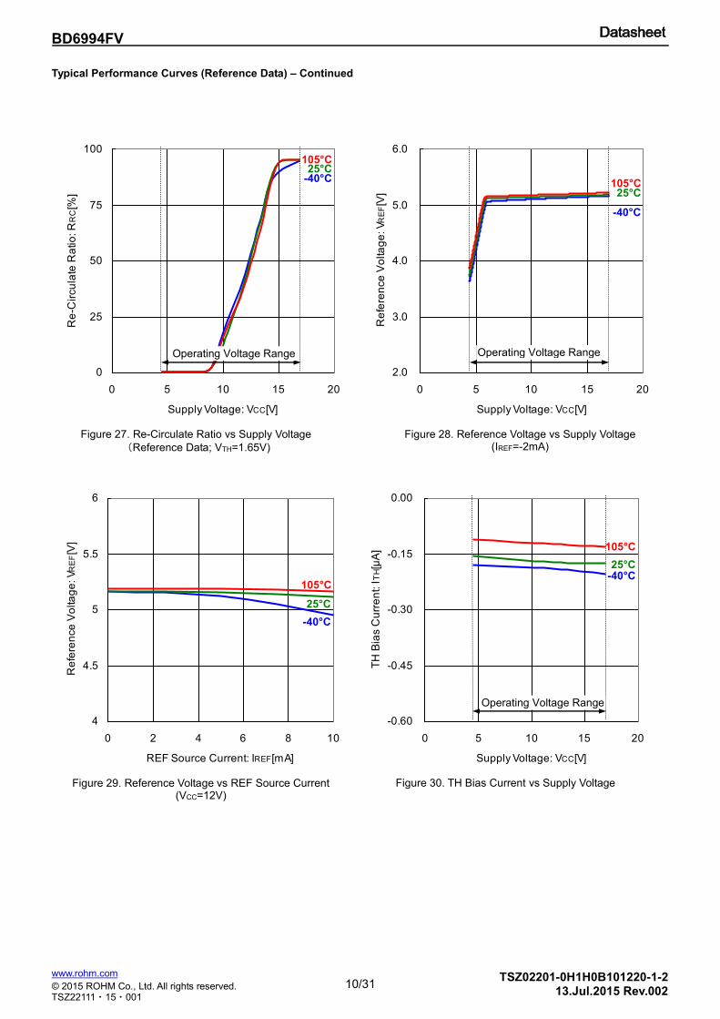
0
25
50
75
100
0 5 10 15 20
Supply Voltage: VCC[V]
Re
-Cir
cu
late
Ra
tio
: R
RC
[%]
4
4.5
5
5.5
6
0 2 4 6 8 10
REF Source Current: IREF[mA]
Re
fere
nce
Vo
lta
ge
: V
RE
F[V
]
-40°C
105°C
25°C
Figure 29. Reference Voltage vs REF Source Current (VCC=12V)
Figure 27. Re-Circulate Ratio vs Supply Voltage
(Reference Data; VTH=1.65V)
-0.60
-0.45
-0.30
-0.15
0.00
0 5 10 15 20
Supply Voltage: VCC[V]
TH
Bia
s C
urr
en
t: I
TH[μ
A]
Operating Voltage Range
-40°C
105°C
25°C
Figure 30. TH Bias Current vs Supply Voltage
Figure 28. Reference Voltage vs Supply Voltage (IREF=-2mA)
-40°C
105°C 25°C
2.0
3.0
4.0
5.0
6.0
0 5 10 15 20
Supply Voltage: VCC[V]
Re
fere
nce
Vo
lta
ge
: V
RE
F[V
]
-40°C
105°C 25°C
Operating Voltage Range Operating Voltage Range
11/31
BD6994FV
© 2015 ROHM Co., Ltd. All rights reserved.
www.rohm.com
TSZ22111・15・001
TSZ02201-0H1H0B101220-1-2 13.Jul.2015 Rev.002
Typical Performance Curves (Reference Data) – Continued
-0.60
-0.45
-0.30
-0.15
0.00
0 5 10 15 20
Supply Voltage: VCC[V]
MIN
Bia
s C
urr
en
t: I
MIN
[μA
]
Operating Voltage Range
-40°C
105°C 25°C
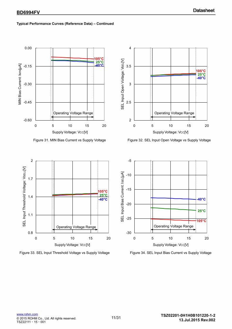
Figure 31. MIN Bias Current vs Supply Voltage
2
2.5
3
3.5
4
0 5 10 15 20
Supply Voltage: VCC[V]
SE
L In
pu
t O
pe
n V
olta
ge
: V
SE
L[V
]
Operating Voltage Range
-40°C
105°C 25°C
Figure 32. SEL Input Open Voltage vs Supply Voltage
0.8
1.1
1.4
1.7
2
0 5 10 15 20
Supply Voltage: VCC[V]
SE
L In
pu
t T
hre
sh
old
Vo
lta
ge
: V
SE
LL[V
]
Operating Voltage Range
-40°C
105°C 25°C
Figure 33. SEL Input Threshold Voltage vs Supply Voltage
-30
-25
-20
-15
-10
-5
0 5 10 15 20
Supply Voltage: VCC[V]
SE
L In
pu
t B
ias C
urr
en
t: I
SE
L[μ
A]
Operating Voltage Range
-40°C
105°C
25°C
Figure 34. SEL Input Bias Current vs Supply Voltage
12/31
BD6994FV
© 2015 ROHM Co., Ltd. All rights reserved.
www.rohm.com
TSZ22111・15・001
TSZ02201-0H1H0B101220-1-2 13.Jul.2015 Rev.002
Typical Performance Curves (Reference Data) – Continued
-50
-40
-30
-20
-10
0 5 10 15 20
Supply Voltage: VCC[V]
PS
In
pu
t B
ias C
urr
en
t: I
PS[μ
A]
2
3
4
5
0 5 10 15 20
Supply Voltage: VCC[V]
PS
In
pu
t O
pe
n V
olta
ge
: V
PS[V
] -40°C
105°C 25°C
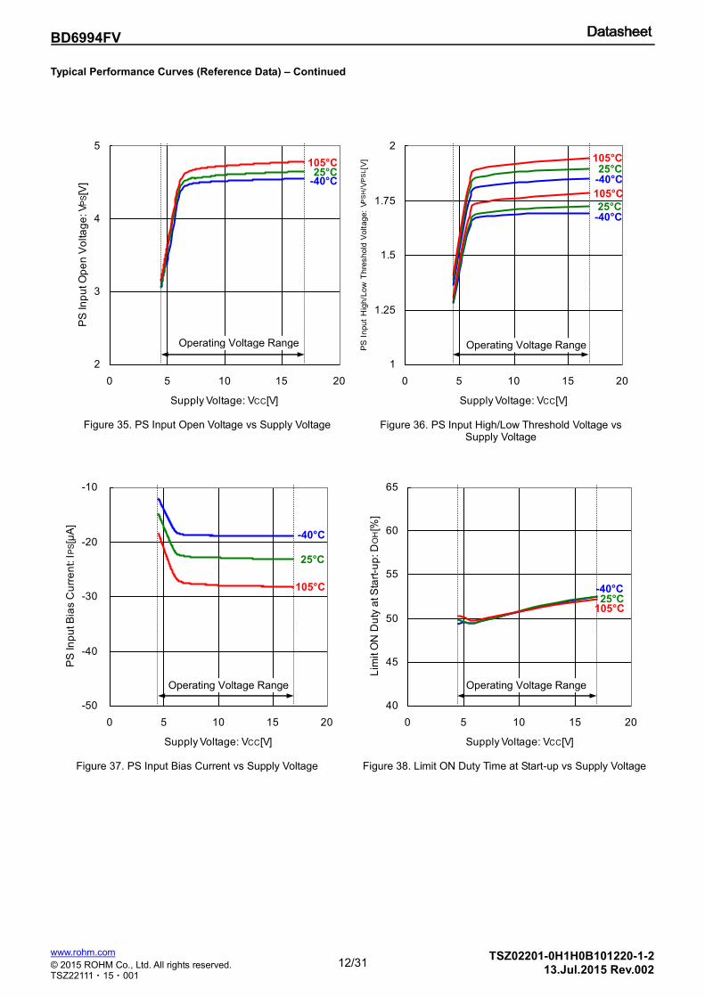
Figure 37. PS Input Bias Current vs Supply Voltage Figure 38. Limit ON Duty Time at Start-up vs Supply Voltage
1
1.25
1.5
1.75
2
0 5 10 15 20
Supply Voltage: VCC[V]
PS
In
pu
t H
igh
/Low
Th
resh
old
Vo
lta
ge
: V
PS
H/V
PS
L[V
]
Operating Voltage Range
-40°C
105°C 25°C
Figure 36. PS Input High/Low Threshold Voltage vs Supply Voltage
105°C
25°C -40°C
Figure 35. PS Input Open Voltage vs Supply Voltage
40
45
50
55
60
65
0 5 10 15 20
Supply Voltage: VCC[V]
Lim
it O
N D
uty
at S
tart
-up
: D
OH
[%]
-40°C
105°C 25°C
-40°C
105°C
25°C
Operating Voltage Range
Operating Voltage Range Operating Voltage Range
13/31
BD6994FV
© 2015 ROHM Co., Ltd. All rights reserved.
www.rohm.com
TSZ22111・15・001
TSZ02201-0H1H0B101220-1-2 13.Jul.2015 Rev.002
Typical Performance Curves (Reference Data) – Continued
20
25
30
35
40
45
0 5 10 15 20
Supply Voltage: VCC[V]
Sta
rt A
ssis
t D
uty
1: D
OH
S1[%
]
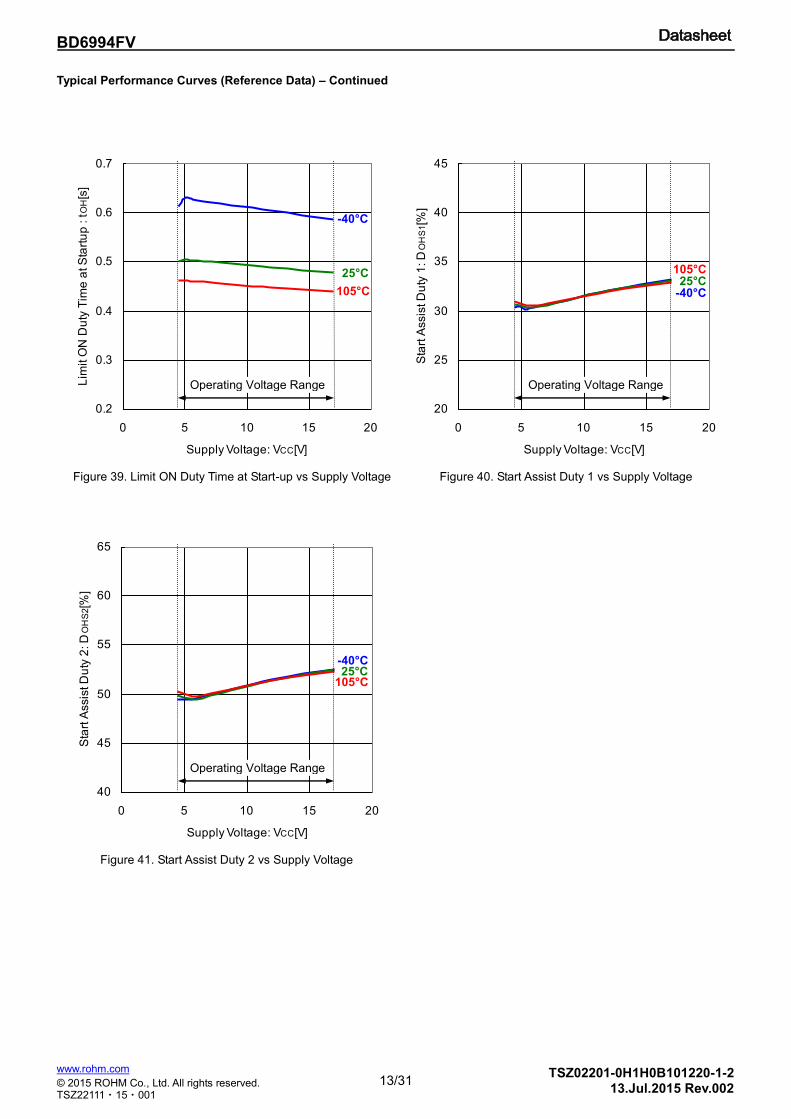
Figure 40. Start Assist Duty 1 vs Supply Voltage
-40°C
105°C 25°C
Operating Voltage Range
Figure 39. Limit ON Duty Time at Start-up vs Supply Voltage
0.2
0.3
0.4
0.5
0.6
0.7
0 5 10 15 20
Supply Voltage: VCC[V]
Lim
it O
N D
uty
Tim
e a
t S
tart
up
: t
OH
[s]
-40°C
105°C
25°C
Operating Voltage Range
40
45
50
55
60
65
0 5 10 15 20
Supply Voltage: VCC[V]
Sta
rt A
ssis
t D
uty
2: D
OH
S2[%
]
Figure 41. Start Assist Duty 2 vs Supply Voltage
-40°C
105°C 25°C
Operating Voltage Range
14/31
BD6994FV
© 2015 ROHM Co., Ltd. All rights reserved.
www.rohm.com
TSZ22111・15・001
TSZ02201-0H1H0B101220-1-2 13.Jul.2015 Rev.002
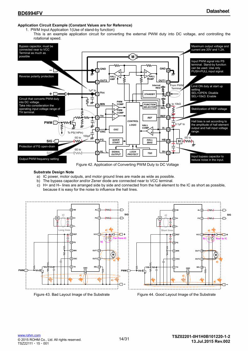
Application Circuit Example (Constant Values are for Reference)
1. PWM Input Application 1(Use of stand-by function) This is an example application circuit for converting the external PWM duty into DC voltage, and controlling the rotational speed.
Substrate Design Note
a) IC power, motor outputs, and motor ground lines are made as wide as possible. b) The bypass capacitor and/or Zener diode are connected near to VCC terminal. c) H+ and H– lines are arranged side by side and connected from the hall element to the IC as short as possible,
because it is easy for the noise to influence the hall lines.
+
M
0.1μF to
1μF to
SIG H 0Ω to 0Ω to
HALL
BIAS
PWM
to 10kΩ
-
0Ω to
SIG
100pF
To PS(14Pin)
From PWM Terminal
HALL AMP
HALL COMP
MIN
TH
OUT1
FG
OSC
Vcc
OUT2
GND
HB
H–
REF
SEL
GND
H+ AL
PS
1
2
3
4
5
6
7
8 9
10
11
12
13
15
16
PWM COMP
PWM COMP
Internal REG
14
OSC
REF
HALL BIAS
SIGNAL OUTPUT
TSD LOCK
PROTECT
QUICK START
CONTROL
LOGIC
FUNCTION SELECTOR
HALL AMP
STANDBY
b)
M
+
-
SIG
H
REF
HB
OUT2
H+
H–
AL
OUT1
VCC
GND
8
11
10
9
2
16
3 12
15
OSC 6
MIN 4
TH 5
a)
a)
a)
PWM
a)
Near to IC
c)
Short lines
HALL
BIAS
FG 7
SEL 13
1
PS 14
b)
M
+
-
SIG
H
REF
HB
OUT2
H+
H–
AL
OUT1
VCC
GND
8
11
10
9
2
16
3 12
15
OSC 6
MIN 4
TH 5
a)
a)
a)
PWM
a)
Far From IC
c)
Long lines
HALL
BIAS
FG 7
SEL 13
1
PS 14
Maximum output voltage and current are 20V and 1.2A.
Hall bias is set according to the amplitude of hall element output and hall input voltage range.
Stabilization of REF voltage
Bypass capacitor, must be connected near to VCC Terminal as much as possible
Circuit that converts PWM duty into DC voltage. Take into consideration the operating input voltage range of TH terminal. .
Input bypass capacitor to reduce noise in the input.
Reverse polarity protection
Limit ON duty at start up setting SEL=OPEN: Disable SEL=10kΩ: Enable
Output PWM frequency setting
Protection of FG open-drain
Figure 42. Application of Converting PWM Duty to DC Voltage
Figure 43. Bad Layout Image of the Substrate Figure 44. Good Layout Image of the Substrate
Input PWM signal into PS terminal. Stand-by function can be used. Use only PUSH-PULL input signal.
15/31
BD6994FV
© 2015 ROHM Co., Ltd. All rights reserved.
www.rohm.com
TSZ22111・15・001
TSZ02201-0H1H0B101220-1-2 13.Jul.2015 Rev.002
Application Circuit Example (Constant Values are for Reference)
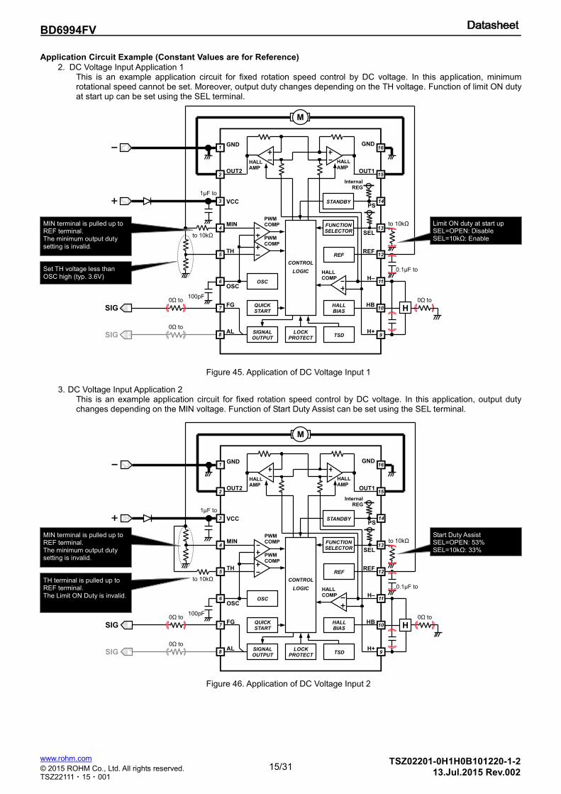
2. DC Voltage Input Application 1 This is an example application circuit for fixed rotation speed control by DC voltage. In this application, minimum rotational speed cannot be set. Moreover, output duty changes depending on the TH voltage. Function of limit ON duty at start up can be set using the SEL terminal.
3. DC Voltage Input Application 2 This is an example application circuit for fixed rotation speed control by DC voltage. In this application, output duty changes depending on the MIN voltage. Function of Start Duty Assist can be set using the SEL terminal.
+
M
0.1μF to
1μF to
SIG H 0Ω to 0Ω to
HALL
BIAS
to 10kΩ
-
0Ω to
SIG
to 10kΩ
100pF
HALL AMP
HALL COMP
MIN
TH
OUT1
FG
OSC
VCC
OUT2
GND
HB
H–
REF
SEL
GND
H+ AL
PS
1
2
3
4
5
6
7
8 9
10
11
12
13
15
16
PWM COMP
PWM COMP
Internal REG
14
OSC
REF
HALL BIAS
SIGNAL OUTPUT
TSD LOCK
PROTECT
QUICK START
CONTROL
LOGIC
FUNCTION SELECTOR
HALL AMP
STANDBY
Figure 45. Application of DC Voltage Input 1
Figure 46. Application of DC Voltage Input 2
Set TH voltage less than OSC high (typ. 3.6V)
MIN terminal is pulled up to REF terminal. The minimum output duty setting is invalid.
Start Duty Assist SEL=OPEN: 53% SEL=10kΩ: 33%
MIN terminal is pulled up to REF terminal. The minimum output duty setting is invalid.
TH terminal is pulled up to REF terminal. The Limit ON Duty is invalid.
Limit ON duty at start up SEL=OPEN: Disable SEL=10kΩ: Enable
16/31
BD6994FV
© 2015 ROHM Co., Ltd. All rights reserved.
www.rohm.com
TSZ22111・15・001
TSZ02201-0H1H0B101220-1-2 13.Jul.2015 Rev.002
Application Circuit Example (Constant Values are for Reference)
4. DC Voltage Input Application 3 (Thermistor Control Application) This is an example application circuit for controlling the rotational speed by ambient temperature. In this application, if the thermistor is OPEN, the IC operates at the set minimum rotational speed. Output duty changes depending on the TH voltage. Function of limit ON duty at start up can be set using the SEL terminal.
5. Pulse Input Application (Use of stand-by function) This is an example application circuit for inverting the external PWM input, and controlling the rotational speed. In this application, if the external PWM input is OPEN, the IC operates at the set maximum rotational speed. Minimum rotational speed cannot be set. The output duty changes depending on MIN. Function of Start Duty Assist can be set using the SEL terminal.
+
M
0.1μF to
1μF to
SIG H 0Ω to
0Ω to
HALL
BIAS
PWM
to 10kΩ
-
0Ω to
SIG
to 10kΩ
100pF
To STBY(14Pin)
From PWM Terminal
HALL AMP
HALL COMP
MIN
TH
OUT1
FG
OSC
VCC
OUT2
GND
HB
H–
REF
SEL
GND
H+ AL
PS
1
2
3
4
5
6
7
8 9
10
11
12
13
15
16
PWM COMP
PWM COMP
Internal REG
14
OSC
REF
HALL BIAS
SIGNAL OUTPUT
TSD LOCK
PROTECT
QUICK START
CONTROL
LOGIC
FUNCTION SELECTOR
HALL AMP
STANDBY
+
M
0.1μF to
1μF to
SIG H 0Ω to
0Ω to
HALL
BIAS
to 10kΩ
-
0Ω to
SIG
100pF
HALL AMP
HALL COMP
MIN
TH
OUT1
FG
OSC
VCC
OUT2
GND
HB
H–
REF
SEL
GND
H+ AL
PS
1
2
3
4
5
6
7
8 9
10
11
12
13
15
16
PWM COMP
PWM COMP
Internal REG
14
OSC
REF
HALL BIAS
SIGNAL OUTPUT
TSD LOCK
PROTECT
QUICK START
CONTROL
LOGIC
FUNCTION SELECTOR
HALL AMP
STANDBY
Figure 48. Application of Pulse Input
Figure 47. Application of Thermistor Control
Set MIN voltage less than OSC high (typ. 3.6V)
Limit ON duty at start up SEL=OPEN: Disable SEL=10kΩ: Enable
Linearization correction resistance if necessary.
The input voltage is changeable in the ambient temperature set by the thermistor constant.
Start Duty Assist SEL=OPEN: 53% SEL=10kΩ: 33%
PWM inversion circuit, Take into consideration the operating input voltage range of MIN terminal.
Circuit that input direct PWM (Ref.) PWM input frequency is 2kHz to 50kHz.
TH terminal is pulled up by REF terminal. The Limit ON Duty is invalid.
Input PWM signal into PS terminal, can use stand-by function. Only in the case of PUSH-PULL input signal.
17/31
BD6994FV
© 2015 ROHM Co., Ltd. All rights reserved.
www.rohm.com
TSZ22111・15・001
TSZ02201-0H1H0B101220-1-2 13.Jul.2015 Rev.002
Functional Descriptions
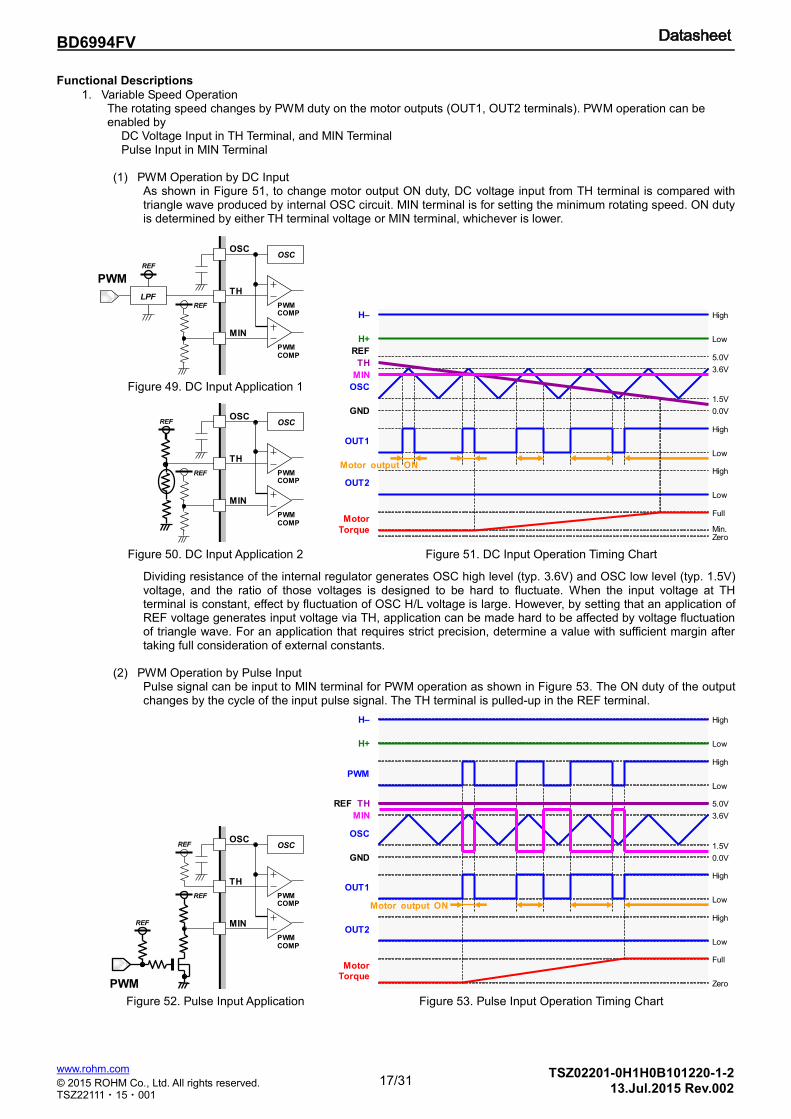
1. Variable Speed Operation The rotating speed changes by PWM duty on the motor outputs (OUT1, OUT2 terminals). PWM operation can be enabled by
DC Voltage Input in TH Terminal, and MIN Terminal Pulse Input in MIN Terminal
(1) PWM Operation by DC Input
As shown in Figure 51, to change motor output ON duty, DC voltage input from TH terminal is compared with triangle wave produced by internal OSC circuit. MIN terminal is for setting the minimum rotating speed. ON duty is determined by either TH terminal voltage or MIN terminal, whichever is lower.
Dividing resistance of the internal regulator generates OSC high level (typ. 3.6V) and OSC low level (typ. 1.5V) voltage, and the ratio of those voltages is designed to be hard to fluctuate. When the input voltage at TH terminal is constant, effect by fluctuation of OSC H/L voltage is large. However, by setting that an application of REF voltage generates input voltage via TH, application can be made hard to be affected by voltage fluctuation of triangle wave. For an application that requires strict precision, determine a value with sufficient margin after taking full consideration of external constants.
(2) PWM Operation by Pulse Input
Pulse signal can be input to MIN terminal for PWM operation as shown in Figure 53. The ON duty of the output changes by the cycle of the input pulse signal. The TH terminal is pulled-up in the REF terminal.
Figure 49. DC Input Application 1
Figure 51. DC Input Operation Timing Chart
Figure 53. Pulse Input Operation Timing Chart Figure 52. Pulse Input Application
Figure 50. DC Input Application 2
REF
OUT1
TH 5.0V
1.5V
3.6V
OUT2
Low
High
Low
High
Low
High
H+
H–
0.0V GND
Zero
Full Motor
Torque
MIN
Min.
OSC
Motor output ON
OSC OSC
TH
PWM COMP
PWM
LPF
PWM COMP
MIN
REF
REF
MIN
REF
OUT1
TH 5.0V
1.5V
3.6V
OUT2
Low
High
Low
High
Low
High
H+
H–
0.0V GND
Low
High
PWM
Zero
Full Motor
Torque
OSC
Motor output ON
OSC OSC
TH
PWM COMP
PWM COMP
MIN
REF
REF
PWM
REF
OSC OSC
TH
PWM COMP
PWM COMP
MIN
REF
REF
18/31
BD6994FV
© 2015 ROHM Co., Ltd. All rights reserved.
www.rohm.com
TSZ22111・15・001
TSZ02201-0H1H0B101220-1-2 13.Jul.2015 Rev.002
Functional Descriptions
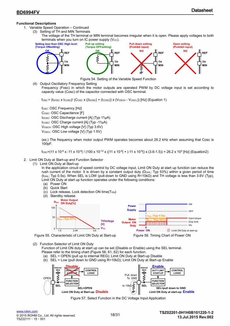
1. Variable Speed Operation – Continued (3) Setting of TH and MIN Terminals
The voltage of the TH terminal or MIN terminal becomes irregular when it is open. Please apply voltages to both terminals when you turn on IC power supply (VCC).
(4) Output Oscillatory Frequency Setting Frequency (Fosc) in which the motor outputs are operated PWM by DC voltage input is set according to capacity value (Cosc) of the capacitor connected with OSC terminal.
fOSC = |IDOSC x ICOSC|/ (COSC x (|IDOSC| + |ICOSC|) x (VOSCH - VOSCL)) [Hz] (Equation 1)
fOSC: OSC Frequency [Hz]
COSC: OSC Capacitance [F]
IDOSC: OSC Discharge current [A] (Typ 11μA)
ICOSC: OSC Charge current [A] (Typ -11μA)
VOSCH: OSC High voltage [V] (Typ 3.6V)
VOSCL: OSC Low voltage [V] (Typ 1.5V)
(ex.) The frequency when motor output PWM operates becomes about 26.2 kHz when assuming that Cosc is 100pF.
fOSC=|11 x 10-6 x -11 x 10-6| / (100 x 10-12 x (|11 x 10-6| + |-11 x 10-6|) x (3.6-1.5)) = 26.2 x 10³ [Hz] (Equation2)
2. Limit ON Duty at Start-up and Function Selector
(1) Limit ON Duty at Start-up In the application circuit of speed control by DC voltage input, Limit ON Duty at start up function can reduce the rush current of the motor. It is driven by a constant output duty (DOHL; Typ 53%) within a given period of time (tOHL; Typ 0.5s). When SEL is LOW (pull-down to GND using R<10kΩ) and TH voltage is less than 3.6V (Typ), Limit ON Duty at start up function operates under the following conditions: (a) Power ON (b) Quick Start (c) Lock release, Lock detection ON time(TON) (d) Standby release
(2) Function Selector of Limit ON Duty Function of Limit ON duty at start up can be set (Disable or Enable) using the SEL terminal. Please refer to the timing chart (Figure 56, 61, 62) for each function. (a) SEL = OPEN (pull up to internal REG); Limit ON Duty at Start-up Disable (b) SEL = Low (pull down to GND using R<10kΩ); Limit ON Duty at Start-up Enable
Figure 56. Timing Chart of Power ON Figure 55. Characteristic of Limit ON Duty at Start-up
Figure 57. Select Function in the DC Voltage Input Application
SEL
FUNCTION SELECTOR
CONTROL LOGIC
DUTY LIMIT
START-UP
SEL=OPEN
Limit ON Duty at Start-up: Disable
Disable
HALL
BIAS
OPEN
Internal
REG
SEL
FUNCTION SELECTOR
CONTROL LOGIC
DUTY LIMIT
START-UP
SEL=pull down to GND
Limit ON Duty at start-up: Enable
Enable
HALL
BIAS
Pull down
To GND
to 10kΩ
Internal
REG
Figure 54. Setting of the Variable Speed Function
NG
TH
Pull down setting (Prohibit input)
MIN
REF
HALL
BIAS
TH
MIN
REF
Pull up setting (Torque OFFsetting)
OK
HALL
BIAS
TH
MIN
REF
Setting less than OSC High level (Torque ONsetting)
OK
TH
MIN
REF NG
Open setting (Prohibit input)
HALL
BIAS
tOHL (Typ 0.5s)
OFF
ON
0%
Input torque Motor Output ON
Duty
Duty limit
Power ON :Limit ON Duty at start-up
Power
Supply
DOHL (Typ 53%)
DOHL (Typ 53%)
1.5
Motor Output
ON Duty[%]
100
0
53
3.6
THVoltage
[V]
VTH
DOH
2.49
19/31
BD6994FV
© 2015 ROHM Co., Ltd. All rights reserved.
www.rohm.com
TSZ22111・15・001
TSZ02201-0H1H0B101220-1-2 13.Jul.2015 Rev.002
Functional Descriptions
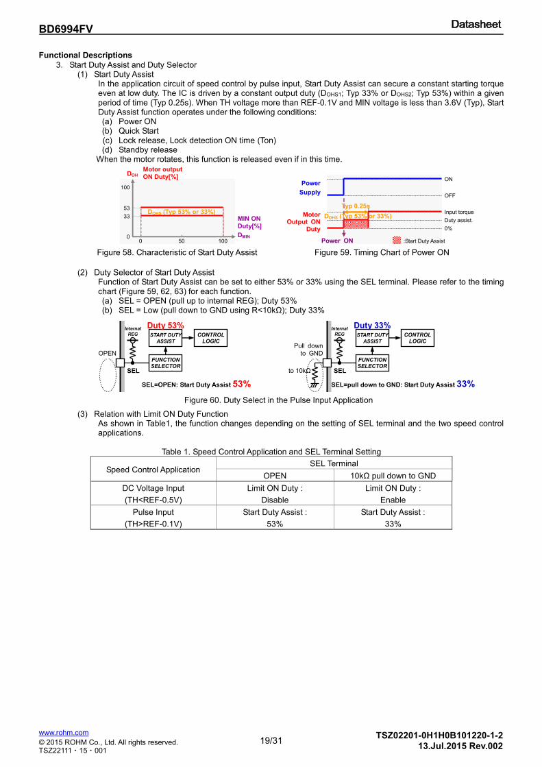
3. Start Duty Assist and Duty Selector (1) Start Duty Assist
In the application circuit of speed control by pulse input, Start Duty Assist can secure a constant starting torque even at low duty. The IC is driven by a constant output duty (DOHS1; Typ 33% or DOHS2; Typ 53%) within a given period of time (Typ 0.25s). When TH voltage more than REF-0.1V and MIN voltage is less than 3.6V (Typ), Start Duty Assist function operates under the following conditions: (a) Power ON (b) Quick Start (c) Lock release, Lock detection ON time (Ton) (d) Standby release When the motor rotates, this function is released even if in this time.
(2) Duty Selector of Start Duty Assist Function of Start Duty Assist can be set to either 53% or 33% using the SEL terminal. Please refer to the timing chart (Figure 59, 62, 63) for each function. (a) SEL = OPEN (pull up to internal REG); Duty 53% (b) SEL = Low (pull down to GND using R<10kΩ); Duty 33%
(3) Relation with Limit ON Duty Function As shown in Table1, the function changes depending on the setting of SEL terminal and the two speed control applications.
Table 1. Speed Control Application and SEL Terminal Setting
Speed Control Application SEL Terminal
OPEN 10kΩ pull down to GND
DC Voltage Input
(TH<REF-0.5V)
Limit ON Duty :
Disable
Limit ON Duty :
Enable
Pulse Input
(TH>REF-0.1V)
Start Duty Assist :
53%
Start Duty Assist :
33%
Figure 60. Duty Select in the Pulse Input Application
Figure 59. Timing Chart of Power ON Figure 58. Characteristic of Start Duty Assist
OFF
ON
0%
Input torque Motor Output ON
Duty
Duty assist.
Power ON :Start Duty Assist
Power
Supply
Typ 0.25s
DOHS (Typ 53% or 33%)
DOHS (Typ 53% or 33%)
0
Motor output
ON Duty[%]
100
0
53
100
MIN ON
Duty[%]
DMIN
DOH
50
33
Pull down
to GND
to 10kΩ SEL
FUNCTION SELECTOR
CONTROL LOGIC
START DUTY
ASSIST
SEL=pull down to GND: Start Duty Assist 33%
Duty 33%
HALL
BIAS
Internal
REG
SEL
FUNCTION SELECTOR
CONTROL LOGIC
START DUTY
ASSIST
SEL=OPEN: Start Duty Assist 53%
Duty 53%
HALL
BIAS
OPEN
Internal
REG
20/31
BD6994FV
© 2015 ROHM Co., Ltd. All rights reserved.
www.rohm.com
TSZ22111・15・001
TSZ02201-0H1H0B101220-1-2 13.Jul.2015 Rev.002
Functional Descriptions
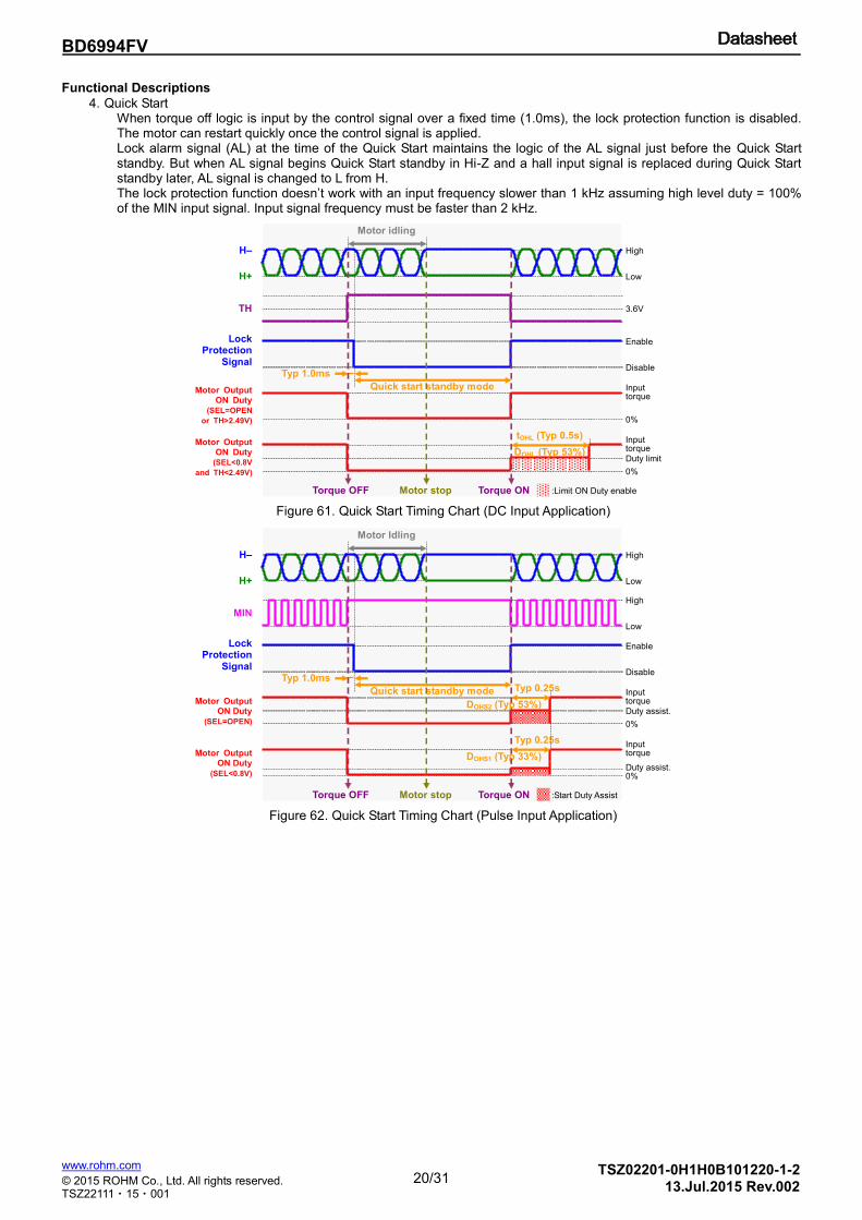
4. Quick Start When torque off logic is input by the control signal over a fixed time (1.0ms), the lock protection function is disabled. The motor can restart quickly once the control signal is applied. Lock alarm signal (AL) at the time of the Quick Start maintains the logic of the AL signal just before the Quick Start standby. But when AL signal begins Quick Start standby in Hi-Z and a hall input signal is replaced during Quick Start standby later, AL signal is changed to L from H. The lock protection function doesn’t work with an input frequency slower than 1 kHz assuming high level duty = 100% of the MIN input signal. Input signal frequency must be faster than 2 kHz.
Figure 61. Quick Start Timing Chart (DC Input Application)
Figure 62. Quick Start Timing Chart (Pulse Input Application)
tOHL (Typ 0.5s)
Disable
Enable
TH 3.6V
Low
High
H+
H–
0%
Typ 1.0ms
Torque OFF Motor stop Torque ON
Lock Protection
Signal
Motor idling
Quick start standby mode
0%
Duty limit
:Limit ON Duty enable
Input torque
Input torque
Motor Output ON Duty
(SEL=OPEN
or TH>2.49V)
Motor Output ON Duty
(SEL<0.8V
and TH<2.49V)
DOHL (Typ 53%)
Typ 0.25s
Typ 0.25s
DOHS1 (Typ 33%)
Disable
Enable
MIN
Low
High
Low
High
H+
H–
Typ 1.0ms
Torque OFF Motor stop Torque ON
Lock Protection
Signal
Motor Idling
Quick start standby mode
0%
:Start Duty Assist
Input torque Motor Output
ON Duty
(SEL=OPEN)
0%
Input torque Motor Output
ON Duty
(SEL<0.8V) Duty assist.
Duty assist. DOHS2 (Typ 53%)
21/31
BD6994FV
© 2015 ROHM Co., Ltd. All rights reserved.
www.rohm.com
TSZ22111・15・001
TSZ02201-0H1H0B101220-1-2 13.Jul.2015 Rev.002
Functional Descriptions
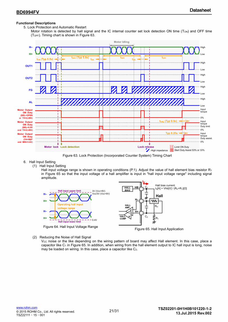
5. Lock Protection and Automatic Restart Motor rotation is detected by hall signal and the IC internal counter set lock detection ON time (TON) and OFF time (TOFF). Timing chart is shown in Figure 63.
6. Hall Input Setting (1) Hall Input Setting
Hall input voltage range is shown in operating conditions (P.1). Adjust the value of hall element bias resistor R1 in Figure 65 so that the input voltage of a hall amplifier is input in "hall input voltage range" including signal amplitude.
(2) Reducing the Noise of Hall Signal VCC noise or the like depending on the wiring pattern of board may affect Hall element. In this case, place a capacitor like C1 in Figure 65. In addition, when wiring from the hall element output to IC hall input is long, noise may be loaded on wiring. In this case, place a capacitor like C2.
H–
HB
H+
Hall
HALL AMP
HALL COMP
C1
C2 R1
RH
IH Hall bias current; IH[A] = Vhb[V] / (RH+R1)[Ω] HALL
BIAS
HALL
BIAS
Figure 63. Lock Protection (Incorporated Counter System) Timing Chart
Figure 65. Hall Input Application Figure 64. Hall Input Voltage Range
Motor Output ON Duty
(SEL=OPEN
or TH>2.49V)
Motor Output ON Duty
(SEL<0.8V
and TH<2.49V)
OUT1
OUT2
H+
H–
Low
High
Low
High
High
Motor lock
Low
High
0%
Input torque
tOFF (Typ 5.0s) tOFF
Motor Idling
Lock detection Lock release
: High impedance
0%
Duty limit
:Limit ON Duty
:Start Duty Assist 53% or 33%
でゅーて
tOHL (Typ 0.5s)
tON (Typ 0.5s) tON
Input torque
tON tOFF
FG
Low
High
AL
Low
Motor Output ON Duty
(TH=REF
and MIN<3.6V) 0%
Duty assist.
Typ 0.25s Input torque
0.4V
Hall input upper limit
H+
H–
Operating hall input
voltage range
Hall input lower limit
H+
H–
3V (Vcc>9V)
Vcc/3V (Vcc<9V)
22/31
BD6994FV
© 2015 ROHM Co., Ltd. All rights reserved.
www.rohm.com
TSZ22111・15・001
TSZ02201-0H1H0B101220-1-2 13.Jul.2015 Rev.002
Functional Descriptions
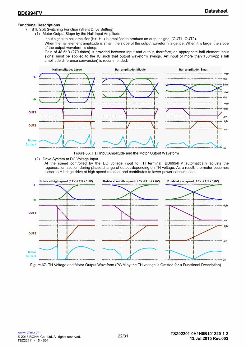
7. BTL Soft Switching Function (Silent Drive Setting) (1) Motor Output Slope by the Hall Input Amplitude
Input signal to hall amplifier (H+, H–) is amplified to produce an output signal (OUT1, OUT2).
When the hall element amplitude is small, the slope of the output waveform is gentle. When it is large, the slope of the output waveform is steep. Gain of 48.5dB (270 times) is provided between input and output, therefore, an appropriate hall element input signal must be applied to the IC such that output waveform swings. An input of more than 150mVpp (Hall amplitude difference conversion) is recommended.
(2) Drive System at DC Voltage Input At the speed controlled by the DC voltage input to TH terminal, BD6994FV automatically adjusts the regeneration section during phase change of output depending on TH voltage. As a result, the motor becomes closer to H bridge drive at high speed rotation, and contributes to lower power consumption
Figure 66. Hall Input Amplitude and the Motor Output Waveform
Figure 67. TH Voltage and Motor Output Waveform (PWM by the TH voltage is Omitted for a Functional Description)
Small
Large
H+
H– Mid.
Small
Large
Mid.
OUT1
OUT2
Low
High
Low
High
0A
Hall amplitude; Large Hall amplitude; Middle Hall amplitude; Small
Motor
Current
H+
H–
OUT1
OUT2
Low
High
Low
High
0A
Rotate at high speed (0.2V < TH < 1.5V) Rotate at middle speed (1.5V < TH < 2.0V) Rotate at low speed (2.0V < TH < 3.6V)
Motor
Current
23/31
BD6994FV
© 2015 ROHM Co., Ltd. All rights reserved.
www.rohm.com
TSZ22111・15・001
TSZ02201-0H1H0B101220-1-2 13.Jul.2015 Rev.002
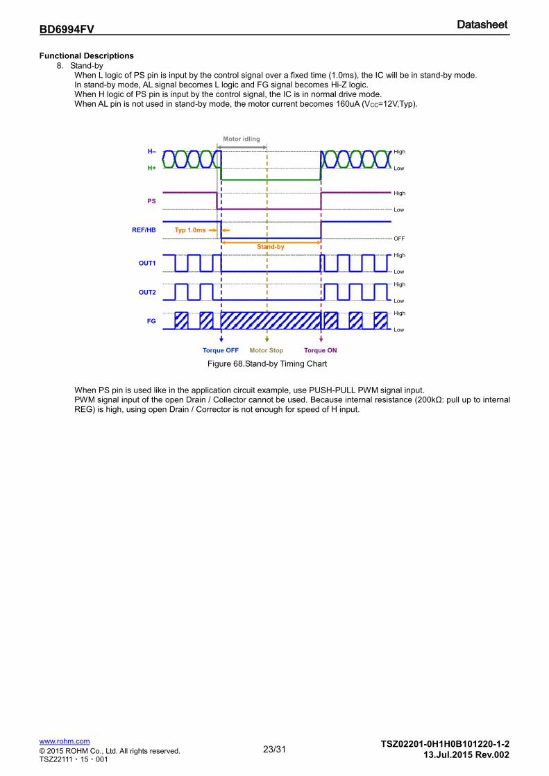
Functional Descriptions
8. Stand-by When L logic of PS pin is input by the control signal over a fixed time (1.0ms), the IC will be in stand-by mode. In stand-by mode, AL signal becomes L logic and FG signal becomes Hi-Z logic. When H logic of PS pin is input by the control signal, the IC is in normal drive mode. When AL pin is not used in stand-by mode, the motor current becomes 160uA (VCC=12V,Typ).
When PS pin is used like in the application circuit example, use PUSH-PULL PWM signal input. PWM signal input of the open Drain / Collector cannot be used. Because internal resistance (200kΩ: pull up to internal REG) is high, using open Drain / Corrector is not enough for speed of H input.
High
Low
PS
Low
High
H+
H–
Typ 1.0ms
Torque OFF Motor Stop
Torque ON
REF/HB
Motor idling
空転
Stand-by
OUT1
OUT2
FG
Low
Low
Low
High
High
High
OFF
Figure 68.Stand-by Timing Chart
24/31
BD6994FV
© 2015 ROHM Co., Ltd. All rights reserved.
www.rohm.com
TSZ22111・15・001
TSZ02201-0H1H0B101220-1-2 13.Jul.2015 Rev.002
Safety Measure
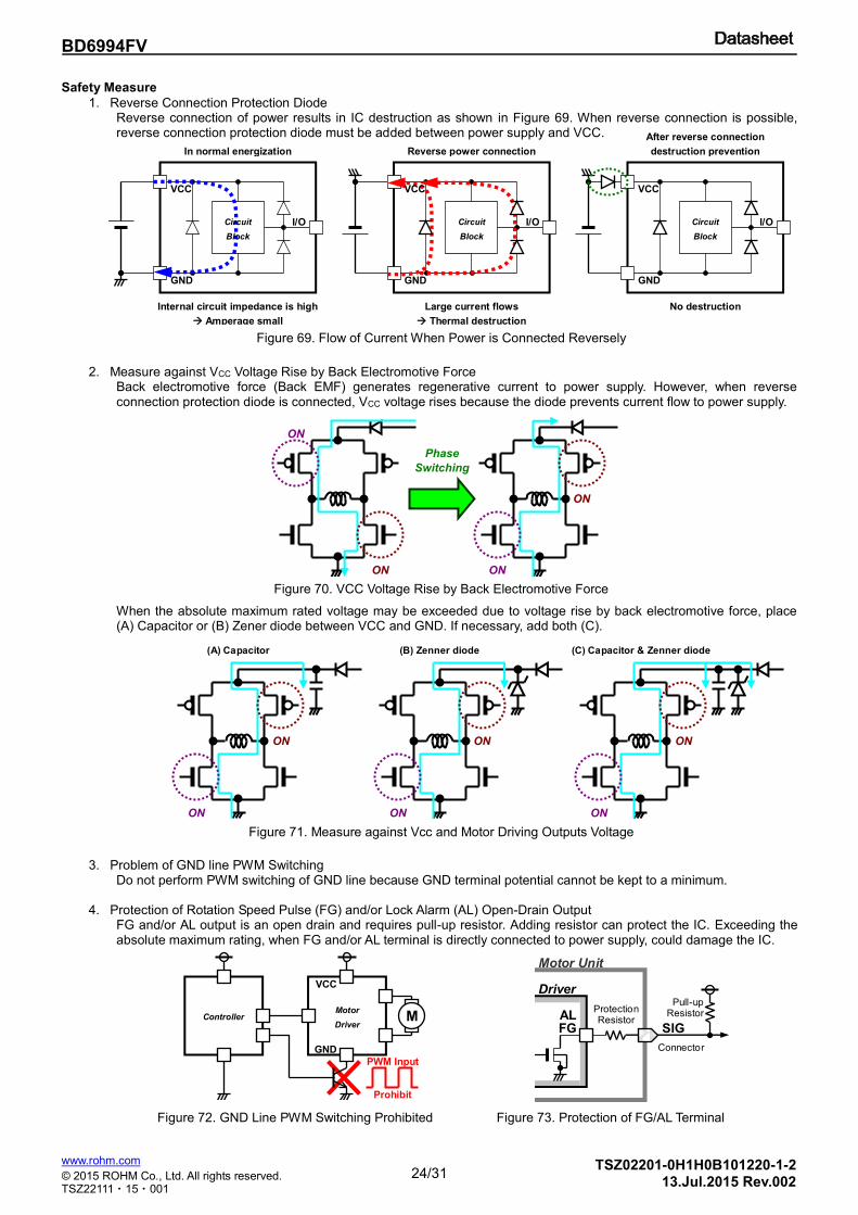
1. Reverse Connection Protection Diode Reverse connection of power results in IC destruction as shown in Figure 69. When reverse connection is possible, reverse connection protection diode must be added between power supply and VCC.
2. Measure against VCC Voltage Rise by Back Electromotive Force Back electromotive force (Back EMF) generates regenerative current to power supply. However, when reverse connection protection diode is connected, VCC voltage rises because the diode prevents current flow to power supply.
When the absolute maximum rated voltage may be exceeded due to voltage rise by back electromotive force, place (A) Capacitor or (B) Zener diode between VCC and GND. If necessary, add both (C).
3. Problem of GND line PWM Switching Do not perform PWM switching of GND line because GND terminal potential cannot be kept to a minimum.
4. Protection of Rotation Speed Pulse (FG) and/or Lock Alarm (AL) Open-Drain Output
FG and/or AL output is an open drain and requires pull-up resistor. Adding resistor can protect the IC. Exceeding the absolute maximum rating, when FG and/or AL terminal is directly connected to power supply, could damage the IC.
Figure 69. Flow of Current When Power is Connected Reversely
Figure 70. VCC Voltage Rise by Back Electromotive Force
Figure 71. Measure against Vcc and Motor Driving Outputs Voltage Rise at Regenerative Braking
Figure 72. GND Line PWM Switching Prohibited Figure 73. Protection of FG/AL Terminal
I/O
VCC
GND
In normal energization
Internal circuit impedance is high
Amperage small
Circuit
Block
HALL BIAS
I/O
GND
Reverse power connection
Large current flows
Thermal destruction
Circuit
Block
VCC
HALL BIAS
I/O
GND
After reverse connection
destruction prevention
No destruction
Circuit
Block
VCC
HALL BIAS
ON
Phase
Switching
ON
ON
ON
ON
ON
ON
ON
ON
ON
(A) Capacitor (B) Zenner diode (C) Capacitor & Zenner diode
VCC
GND
Prohibit
Motor
Driver Controller
PWM Input
M
HALL BIAS
FG
Driver
AL Protection Resistor
Motor Unit
Pull-up Resistor
SIG
Connector
25/31
BD6994FV
© 2015 ROHM Co., Ltd. All rights reserved.
www.rohm.com
TSZ22111・15・001
TSZ02201-0H1H0B101220-1-2 13.Jul.2015 Rev.002
Power Consumption
1. Current Pathway The current pathways that relates to driver IC are the following, and shown in Figure 74. (1) Circuit Current (ICC) (2) Motor Driving Current (IM) (3) Reference Bias Current to the LPF and Resistors (IREF)
(4) Hall Bias Current to the Hall Element (IHB) (5) FG(AL) Output Sink Current (ISO)
2. Calculation of Power Consumption (1) Circuit Current (Icc)
PW(a) = VCC x ICC [W] (Equation3)
PW(a): Power consumption [W]
VCC: VCC voltage [V]
ICC: Circuit current [A]
(Expect hall bias current (IHB))
(2) Motor Driving Current (IM)
PW(b) = ((VOH+VOL) x IM) x T2/T1 + (ICHANGE / 2 x VCC / 4) x T3/ T1 [W] (Equation4) PW(b): Power consumption [W] VOH: Output high voltage [V] VOL: Output low voltage [V] IM: Motor driving average current [A] ICHANGE: Motor driving current of BTL initiation [A]
(3) Reference Bias Current to the LPF and Resistors (IREF)
PW(c) = (VCC - VREF) x IREF [W] (Equation5) PW(c): Power consumption [W] VREF: REF voltage [V] IREF: REF bias current [A]
(4) Hall Bias Current to the Hall Element (IHB)
PW(d) = (VCC - VHB) x IHB [W] (Equation6) PW(d): Power consumption [W] VHB: Hall bias voltage [V] IHB: Hall bias current [A]
(5) FG(AL) Output Sink Current (Iso) PW(e) = VSO x ISO [W] (Equation7)
PW(e): Power consumption [W] VSO: FG(AL) output low voltage [V] ISO: FG(AL) output sink current [A]
Total power consumption of driver IC becomes the following by the above (1) to (5).
PW(ttl) = PW(a) + PW(b) + PW(c) + PW(d) + PW(e) [W] (Equation8) (ex.)
PW(a) = 12 x 6.5 x 10-3 [W] (Equation9) PW(b) = ((0.37 + 0.23) x 0.4) x 9/10 + (0.4/2 x 12/4) x 1/10 [W] (Equation10) PW(c) = (12 - 5.1) x 2.0 x10-3 [W] (Equation11) PW(d) = (12 - 1.25) x 3.5 x 10-3 [W] (Equation12) PW(e) = 0.2 x 5.0 x 10-3 [W] (Equation13) PW(ttl) = 0.406 [W] (Equation14)
Refer to next page when you calculate the chip surface temperature (Tj) and the package surface temperature (Tc) by using the power consumption value.
Figure 74. Current Pathway of IC
HALL BIAS
+
M
SIG H
PWM
-
SIG
IHB ISO
IM
ICC
IREF
HALL AMP
HALL COMP
MIN
TH
OUT1
FG
OSC
VCC
OUT2
GND
HB
H–
REF
SEL
GND
H+ AL
PS
1
2
3
4
5
6
7
8 9
10
11
12
13
15
16
PWM COMP
PWM COMP
Internal REG
14
OSC
REF
HALL BIAS
SIGNAL OUTPUT
TSD LOCK
PROTECT
QUICK START
CONTROL
LOGIC
FUNCTION SELECTOR
HALL AMP
STANDBY
H+
H–
OUT1
OUT2
T2 T3
T1
Im
I Change
Figure 75. Motor Driving Current for calculation
26/31
BD6994FV
© 2015 ROHM Co., Ltd. All rights reserved.
www.rohm.com
TSZ22111・15・001
TSZ02201-0H1H0B101220-1-2 13.Jul.2015 Rev.002
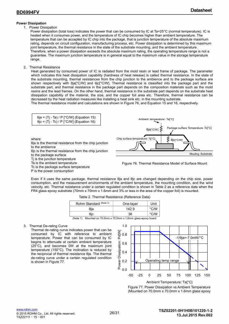
Power Dissipation
1. Power Dissipation Power dissipation (total loss) indicates the power that can be consumed by IC at Ta=25°C (normal temperature). IC is heated when it consumes power, and the temperature of IC chip becomes higher than ambient temperature. The temperature that can be accepted by IC chip into the package, that is junction temperature of the absolute maximum rating, depends on circuit configuration, manufacturing process, etc. Power dissipation is determined by this maximum joint temperature, the thermal resistance in the state of the substrate mounting, and the ambient temperature. Therefore, when a power dissipation exceeds the absolute maximum rating, the operating temperature range is not a guarantee. The maximum junction temperature is in general equal to the maximum value in the storage temperature range.
2. Thermal Resistance
Heat generated by consumed power of IC is radiated from the mold resin or lead frame of package. The parameter which indicates this heat dissipation capability (hardness of heat release) is called thermal resistance. In the state of the substrate mounting, thermal resistances from the chip junction to the ambience and to the package surface are shown respectively with θja[°C/W] and θjc[°C/W]. Thermal resistance is classified into the package part and the substrate part, and thermal resistance in the package part depends on the composition materials such as the mold resins and the lead frames. On the other hand, thermal resistance in the substrate part depends on the substrate heat dissipation capability of the material, the size, and the copper foil area etc. Therefore, thermal resistance can be decreased by the heat radiation measures like installing a heat sink etc. in the mounting substrate. The thermal resistance model and calculations are shown in Figure 76, and Equation 15 and 16, respectively.
where: θja is the thermal resistance from the chip junction to the ambience θjc is the thermal resistance from the chip junction to the package surface Tj is the junction temperature Ta is the ambient temperature Tc is the package surface temperature P is the power consumption
Even if it uses the same package, thermal resistance θja and θjc are changed depending on the chip size, power consumption, and the measurement environments of the ambient temperature, the mounting condition, and the wind velocity, etc. Thermal resistance under a certain regulated condition is shown in Table 2 as a reference data when the FR4 glass epoxy substrate (70mm x 70mm x 1.6mm and 3% or less in the area of the copper foil) is mounted.
Rohm Standard (Note 1) One-layer Unit
θja 142.9 °C/W
θjc 36 °C/W (Note 1) Mounted on 70.0mm x 70.0mm x 1.6mm glass epoxy board
3. Thermal De-rating Curve
Thermal de-rating curve indicates power that can be consumed by IC with reference to ambient temperature. Power that can be consumed by IC begins to attenuate at certain ambient temperature (25°C), and becomes 0W at the maximum joint temperature (150°C). The inclination is reduced by the reciprocal of thermal resistance θja. The thermal de-rating curve under a certain regulated condition is shown in Figure 77.
Figure 76. Thermal Resistance Model of Surface Mount
Table 2. Thermal Resistance (Reference Data)
θjc[°C/W] Chip surface temperature: Tj[°C]
Package surface Temperature: Tc[°C]
Ambient temperature: Ta[°C]
θja[°C/W]
Mouting Substrate
HALL
BIAS
0.0
0.2
0.4
0.6
0.8
1.0
-50 -25 0 25 50 75 100 125 150
Ambient Temperature: Ta[°C]
Po
we
r D
issip
atio
n: P
d[W
]
Operating temp range
Figure 77. Power Dissipation vs Ambient Temperature (Mounted on 70.0mm x 70.0mm x 1.6mm glass epoxy
substrate)
-1/θja=-7.0mW/°C
θja = (Tj - Ta) / P [°C/W] (Equation 15)
θjc = (Tj - Tc) / P [°C/W] (Equation 16)
27/31
BD6994FV
© 2015 ROHM Co., Ltd. All rights reserved.
www.rohm.com
TSZ22111・15・001
TSZ02201-0H1H0B101220-1-2 13.Jul.2015 Rev.002
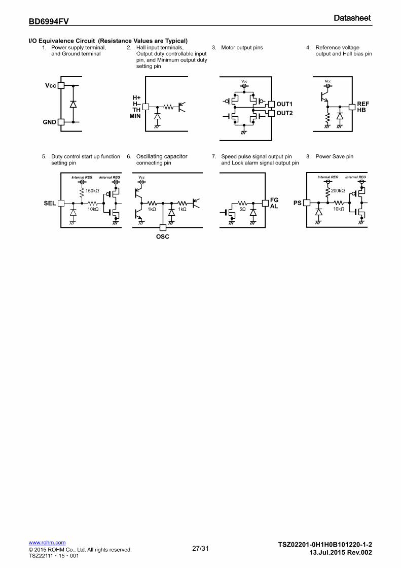
I/O Equivalence Circuit (Resistance Values are Typical) 1. Power supply terminal, 2. Hall input terminals, 3. Motor output pins 4. Reference voltage and Ground terminal Output duty controllable input output and Hall bias pin pin, and Minimum output duty setting pin
5. Duty control start up function 6. Oscillating capacitor 7. Speed pulse signal output pin 8. Power Save pin setting pin connecting pin and Lock alarm signal output pin
Vcc
OUT1
OUT2
Vcc
GND
REF
Vcc
HB
HALL
BIAS
OSC
Vcc
1kΩ 1kΩ
SEL 10kΩ
150kΩ
Internal REG Internal REG
5Ω
FG AL
TH
1kΩ
H+ H–
MIN
PS 10kΩ
200kΩ
Internal REG Internal REG
HALL
BIAS
28/31
BD6994FV
© 2015 ROHM Co., Ltd. All rights reserved.
www.rohm.com
TSZ22111・15・001
TSZ02201-0H1H0B101220-1-2 13.Jul.2015 Rev.002
Operational Notes
1. Reverse Connection of Power Supply Connecting the power supply in reverse polarity can damage the IC. Take precautions against reverse polarity when connecting the power supply, such as mounting an external diode between the power supply and the IC’s power supply pins.
2. Power Supply Lines
Design the PCB layout pattern to provide low impedance supply lines. Separate the ground and supply lines of the digital and analog blocks to prevent noise in the ground and supply lines of the digital block from affecting the analog block furthermore, connect a capacitor to ground at all power supply pins. Consider the effect of temperature and aging on the capacitance value when using electrolytic capacitors.
3. Ground Voltage
Ensure that no pins are at a voltage below that of the ground pin at any time, even during transient condition. However, pins that drive inductive loads (e.g. motor driver outputs, DC-DC converter outputs) may inevitably go below ground due to back EMF or electromotive force. In such cases, the user should make sure that such voltages going below ground will not cause the IC and the system to malfunction by examining carefully all relevant factors and conditions such as motor characteristics, supply voltage, operating frequency and PCB wiring to name a few.
4. Ground Wiring Pattern
When using both small-signal and large-current ground traces, the two ground traces should be routed separately but connected to a single ground at the reference point of the application board to avoid fluctuations in the small-signal ground caused by large currents. Also ensure that the ground traces of external components do not cause variations on the ground voltage the ground lines must be as short and thick as possible to reduce line impedance.
5. Thermal Consideration
Should by any chance the power dissipation rating be exceeded the rise in temperature of the chip may result in deterioration of the properties of the chip. The absolute maximum rating of the power dissipation stated in this datasheet is when the IC is mounted on a 70mm x 70mm x 1.6mm glass epoxy board. In case of exceeding this absolute maximum rating, increase the board size and copper area to raise heat dissipation capability.
6. Recommended Operating Conditions
These conditions represent a range within which the expected characteristics of the IC can be approximately obtained. The electrical characteristics are guaranteed under the conditions of each parameter.
7. Inrush Current
When power is first supplied to the IC, it is possible that the internal logic may be unstable and inrush current may flow instantaneously due to the internal powering sequence and delays, especially if the IC has more than one power supply. Therefore, give special consideration to power coupling capacitance, width of power and ground wiring, and routing of connections.
8. Operation Under Strong Electromagnetic Field
Operating the IC in the presence of a strong electromagnetic field may cause the IC to malfunction. 9. Testing on Application Boards
When testing the IC on an application board, connecting a capacitor directly to a low-impedance output pin may subject the IC to stress. Always discharge capacitors completely after each process or step. To prevent damage from static discharge, ground the IC during assembly and use similar precautions during transport and storage. The IC’s power supply should always be turned off completely before connecting or removing it from the test setup during the inspection process.
10. Mounting Errors and Inter-pin Short
Ensure that the direction and position are correct when mounting the IC on the PCB. Incorrect mounting may result in damaging the IC. Avoid nearby pins being shorted to each other especially to ground, power supply and output pin. Inter-pin shorts could be due to many reasons such as metal particles, water droplets (in very humid environment) and unintentional solder bridge deposited in between pins during assembly to name a few.
29/31
BD6994FV
© 2015 ROHM Co., Ltd. All rights reserved.
www.rohm.com
TSZ22111・15・001
TSZ02201-0H1H0B101220-1-2 13.Jul.2015 Rev.002
Operational Notes
11. Unused Input Pins Input pins of an IC are often connected to the gate of a MOS transistor. The gate has extremely high impedance and extremely low capacitance. If left unconnected, the electric field from the outside can easily charge it. The small charge acquired in this way is enough to produce a significant effect on the conduction through the transistor and cause unexpected operation of the IC. Especially, if it is not expressed on the datasheet, unused input pins should be connected to the power supply or ground line.
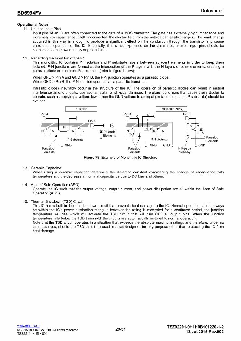
12. Regarding the Input Pin of the IC
This monolithic IC contains P+ isolation and P substrate layers between adjacent elements in order to keep them isolated. P-N junctions are formed at the intersection of the P layers with the N layers of other elements, creating a parasitic diode or transistor. For example (refer to figure below):
When GND > Pin A and GND > Pin B, the P-N junction operates as a parasitic diode. When GND > Pin B, the P-N junction operates as a parasitic transistor.
Parasitic diodes inevitably occur in the structure of the IC. The operation of parasitic diodes can result in mutual interference among circuits, operational faults, or physical damage. Therefore, conditions that cause these diodes to operate, such as applying a voltage lower than the GND voltage to an input pin (and thus to the P substrate) should be avoided.
13. Ceramic Capacitor
When using a ceramic capacitor, determine the dielectric constant considering the change of capacitance with temperature and the decrease in nominal capacitance due to DC bias and others.
14. Area of Safe Operation (ASO)
Operate the IC such that the output voltage, output current, and power dissipation are all within the Area of Safe Operation (ASO).
15. Thermal Shutdown (TSD) Circuit
This IC has a built-in thermal shutdown circuit that prevents heat damage to the IC. Normal operation should always be within the IC’s power dissipation rating. If however the rating is exceeded for a continued period, the junction temperature will rise which will activate the TSD circuit that will turn OFF all output pins. When the junction temperature falls below the TSD threshold, the circuits are automatically restored to normal operation. Note that the TSD circuit operates in a situation that exceeds the absolute maximum ratings and therefore, under no circumstances, should the TSD circuit be used in a set design or for any purpose other than protecting the IC from heat damage.
Figure 78. Example of Monolithic IC Structure
N NP
+ P
N NP
+
P Substrate
GND
NP
+
N NP
+N P
P Substrate
GND GND
Parasitic
Elements
Pin A
Pin A
Pin B Pin B
B C
E
Parasitic
Elements
GNDParasitic
Elements
CB
E
Transistor (NPN)Resistor
N Region
close-by
Parasitic
Elements
30/31
BD6994FV
© 2015 ROHM Co., Ltd. All rights reserved.
www.rohm.com
TSZ22111・15・001
TSZ02201-0H1H0B101220-1-2 13.Jul.2015 Rev.002
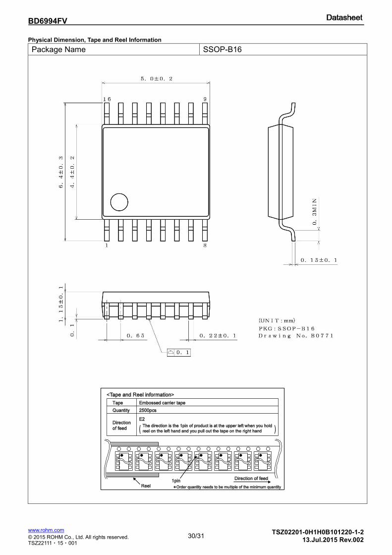
Physical Dimension, Tape and Reel Information
Package Name SSOP-B16
31/31
BD6994FV
© 2015 ROHM Co., Ltd. All rights reserved.
www.rohm.com
TSZ22111・15・001
TSZ02201-0H1H0B101220-1-2 13.Jul.2015 Rev.002
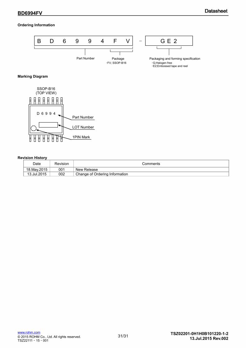
Ordering Information
Marking Diagram
Revision History
Date Revision Comments
18.May.2015 001 New Release
13.Jul.2015 002 Change of Ordering Information
D 6 9 9 4
SSOP-B16 (TOP VIEW)
Part Number
LOT Number
1PIN Mark
B D 6 9 4 F G
Part Number Package
・FV; SSOP-B16
V
・G;Halogen free
Packaging and forming specification
-
9 2 E
・E2;Embossed tape and reel
DatasheetDatasheet
Notice-PGA-E Rev.001© 2015 ROHM Co., Ltd. All rights reserved.
Notice Precaution on using ROHM Products
1. Our Products are designed and manufactured for application in ordinary electronic equipments (such as AV equipment, OA equipment, telecommunication equipment, home electronic appliances, amusement equipment, etc.). If you intend to use our Products in devices requiring extremely high reliability (such as medical equipment (Note 1), transport equipment, traffic equipment, aircraft/spacecraft, nuclear power controllers, fuel controllers, car equipment including car accessories, safety devices, etc.) and whose malfunction or failure may cause loss of human life, bodily injury or serious damage to property (“Specific Applications”), please consult with the ROHM sales representative in advance. Unless otherwise agreed in writing by ROHM in advance, ROHM shall not be in any way responsible or liable for any damages, expenses or losses incurred by you or third parties arising from the use of any ROHM’s Products for Specific Applications.
(Note1) Medical Equipment Classification of the Specific Applications JAPAN USA EU CHINA
CLASSⅢ CLASSⅢ
CLASSⅡb CLASSⅢ
CLASSⅣ CLASSⅢ
2. ROHM designs and manufactures its Products subject to strict quality control system. However, semiconductor
products can fail or malfunction at a certain rate. Please be sure to implement, at your own responsibilities, adequate safety measures including but not limited to fail-safe design against the physical injury, damage to any property, which a failure or malfunction of our Products may cause. The following are examples of safety measures:
[a] Installation of protection circuits or other protective devices to improve system safety [b] Installation of redundant circuits to reduce the impact of single or multiple circuit failure
3. Our Products are designed and manufactured for use under standard conditions and not under any special or extraordinary environments or conditions, as exemplified below. Accordingly, ROHM shall not be in any way responsible or liable for any damages, expenses or losses arising from the use of any ROHM’s Products under any special or extraordinary environments or conditions. If you intend to use our Products under any special or extraordinary environments or conditions (as exemplified below), your independent verification and confirmation of product performance, reliability, etc, prior to use, must be necessary:
[a] Use of our Products in any types of liquid, including water, oils, chemicals, and organic solvents [b] Use of our Products outdoors or in places where the Products are exposed to direct sunlight or dust [c] Use of our Products in places where the Products are exposed to sea wind or corrosive gases, including Cl2,
H2S, NH3, SO2, and NO2
[d] Use of our Products in places where the Products are exposed to static electricity or electromagnetic waves [e] Use of our Products in proximity to heat-producing components, plastic cords, or other flammable items [f] Sealing or coating our Products with resin or other coating materials [g] Use of our Products without cleaning residue of flux (even if you use no-clean type fluxes, cleaning residue of
flux is recommended); or Washing our Products by using water or water-soluble cleaning agents for cleaning residue after soldering
[h] Use of the Products in places subject to dew condensation
4. The Products are not subject to radiation-proof design. 5. Please verify and confirm characteristics of the final or mounted products in using the Products. 6. In particular, if a transient load (a large amount of load applied in a short period of time, such as pulse. is applied,
confirmation of performance characteristics after on-board mounting is strongly recommended. Avoid applying power exceeding normal rated power; exceeding the power rating under steady-state loading condition may negatively affect product performance and reliability.
7. De-rate Power Dissipation (Pd) depending on Ambient temperature (Ta). When used in sealed area, confirm the actual
ambient temperature. 8. Confirm that operation temperature is within the specified range described in the product specification. 9. ROHM shall not be in any way responsible or liable for failure induced under deviant condition from what is defined in
this document.
Precaution for Mounting / Circuit board design 1. When a highly active halogenous (chlorine, bromine, etc.) flux is used, the residue of flux may negatively affect product
performance and reliability.
2. In principle, the reflow soldering method must be used on a surface-mount products, the flow soldering method must be used on a through hole mount products. If the flow soldering method is preferred on a surface-mount products, please consult with the ROHM representative in advance.
For details, please refer to ROHM Mounting specification

DatasheetDatasheet
Notice-PGA-E Rev.001© 2015 ROHM Co., Ltd. All rights reserved.
Precautions Regarding Application Examples and External Circuits 1. If change is made to the constant of an external circuit, please allow a sufficient margin considering variations of the
characteristics of the Products and external components, including transient characteristics, as well as static characteristics.
2. You agree that application notes, reference designs, and associated data and information contained in this document
are presented only as guidance for Products use. Therefore, in case you use such information, you are solely responsible for it and you must exercise your own independent verification and judgment in the use of such information contained in this document. ROHM shall not be in any way responsible or liable for any damages, expenses or losses incurred by you or third parties arising from the use of such information.
Precaution for Electrostatic
This Product is electrostatic sensitive product, which may be damaged due to electrostatic discharge. Please take proper caution in your manufacturing process and storage so that voltage exceeding the Products maximum rating will not be applied to Products. Please take special care under dry condition (e.g. Grounding of human body / equipment / solder iron, isolation from charged objects, setting of Ionizer, friction prevention and temperature / humidity control).
Precaution for Storage / Transportation 1. Product performance and soldered connections may deteriorate if the Products are stored in the places where:
[a] the Products are exposed to sea winds or corrosive gases, including Cl2, H2S, NH3, SO2, and NO2 [b] the temperature or humidity exceeds those recommended by ROHM [c] the Products are exposed to direct sunshine or condensation [d] the Products are exposed to high Electrostatic
2. Even under ROHM recommended storage condition, solderability of products out of recommended storage time period may be degraded. It is strongly recommended to confirm solderability before using Products of which storage time is exceeding the recommended storage time period.
3. Store / transport cartons in the correct direction, which is indicated on a carton with a symbol. Otherwise bent leads
may occur due to excessive stress applied when dropping of a carton. 4. Use Products within the specified time after opening a humidity barrier bag. Baking is required before using Products of
which storage time is exceeding the recommended storage time period.
Precaution for Product Label QR code printed on ROHM Products label is for ROHM’s internal use only.
Precaution for Disposition When disposing Products please dispose them properly using an authorized industry waste company.
Precaution for Foreign Exchange and Foreign Trade act Since concerned goods might be fallen under listed items of export control prescribed by Foreign exchange and Foreign trade act, please consult with ROHM in case of export.
Precaution Regarding Intellectual Property Rights 1. All information and data including but not limited to application example contained in this document is for reference
only. ROHM does not warrant that foregoing information or data will not infringe any intellectual property rights or any other rights of any third party regarding such information or data.
2. ROHM shall not have any obligations where the claims, actions or demands arising from the combination of the Products with other articles such as components, circuits, systems or external equipment (including software).
3. No license, expressly or implied, is granted hereby under any intellectual property rights or other rights of ROHM or any third parties with respect to the Products or the information contained in this document. Provided, however, that ROHM will not assert its intellectual property rights or other rights against you or your customers to the extent necessary to manufacture or sell products containing the Products, subject to the terms and conditions herein.
Other Precaution 1. This document may not be reprinted or reproduced, in whole or in part, without prior written consent of ROHM.
2. The Products may not be disassembled, converted, modified, reproduced or otherwise changed without prior written consent of ROHM.
3. In no event shall you use in any way whatsoever the Products and the related technical information contained in the Products or this document for any military purposes, including but not limited to, the development of mass-destruction weapons.
4. The proper names of companies or products described in this document are trademarks or registered trademarks of ROHM, its affiliated companies or third parties.
DatasheetDatasheet
Notice – WE Rev.001© 2015 ROHM Co., Ltd. All rights reserved.
General Precaution 1. Before you use our Pro ducts, you are requested to care fully read this document and fully understand its contents.
ROHM shall n ot be in an y way responsible or liabl e for fa ilure, malfunction or acci dent arising from the use of a ny ROHM’s Products against warning, caution or note contained in this document.
2. All information contained in this docume nt is current as of the issuing date and subj ect to change without any prior
notice. Before purchasing or using ROHM’s Products, please confirm the la test information with a ROHM sale s representative.
3. The information contained in this doc ument is provi ded on an “as is” basis and ROHM does not warrant that all
information contained in this document is accurate an d/or error-free. ROHM shall not be in an y way responsible or liable for any damages, expenses or losses incurred by you or third parties resulting from inaccuracy or errors of or concerning such information.