Embed Size (px)
Citation preview

TGA4542 37 - 40 GHz 1W Power Amplifier
Preliminary Data Sheet: Rev - 9/15/12 - 1 of 12 - Disclaimer: Subject to change without notice
© 2012 TriQuint Semiconductor, Inc. Connecting the Digital World to the Global Network®
Applications
Point to Point Radio
Millimeter-wave Communications
Military & Space
Product Features Functional Block Diagram
Frequency range: 37 - 40 GHz
Output Power: 32.5 dBm Psat, 31.5 dBm P1dB
Gain: 26 dBm Typical
TOI: 38 dBm @ 18 dBm Output/Tone
Integrated Power Detector
Bias: Vcc = 6V, Icc = 900 mA Typical
Dimension: 2.95 x 2.95 x 0.1 mm
General Description Bond Pad Configuration
The TriQuint TGA4542 is a 37 - 40 GHz Power Amplifier designed using TriQuint’s power pHEMT production process. The TGA4542 typically provides 31.5 dBm of output power at 1dB gain compression with small signal gain of 26 dB. Third Order Intercept is 38 dBm at 18 dBm Output/Tone. The TGA4542 is ideally suited for Point-to-Point Radio, Ka-band communications, and Millimeter-wave communications. Lead-free and RoHS compliant. Evaluation Boards are available upon request.
Bond Pad # Function Label
1 RF In
2, 14 Vg
3, 4, 5, 6, 10, 11, 12, 13 Vd
7 RF Out
8 Vdet
9 Vref
Ordering Information
Part No. ECCN Description
TGA4542 3A001.b.2.e 37 - 40 GHz 1W Power Amplifier
Standard order qty = 50 pieces.
1 7
8
10 9
2 63 4 5
14 13 12 11
Vg Vd1 Vd2 Vd3 Vd4
Vg
RF In RF Out
Vd1 Vd2 Vd3 Vd4 Vref
Vdet
TGA4542 37 - 40 GHz 1W Power Amplifier
Preliminary Data Sheet: Rev - 9/15/12 - 2 of 12 - Disclaimer: Subject to change without notice
© 2012 TriQuint Semiconductor, Inc. Connecting the Digital World to the Global Network®
Specifications
Absolute Maximum Ratings
Parameter Rating Drain to Gate Voltage, Vd - Vg 10V
Drain Voltage, Vd +6.5 V
Gate Voltage, Vg -4 to 0 V
Drain Current, Id 2086 mA
Gate Current, Ig -8.2 to 113 mA
Power Dissipation, Pdiss 13.6 W
RF Input Power, CW, 50Ω, T=25°C
26 dBm
Channel Temperature, Tch 200°C
Mounting Temperature (30 Seconds)
320°C
Storage Temperature -40 to 150C
Operation of this device outside the parameter ranges given above may cause permanent damage.
Recommended Operating Conditions
Parameter Min Typ Max Units
Operating Temp. Range -40 +25 +85 C
Vd 6.0 V
Id 900 mA
Id (Under RF Drive) 1500 mA
Vg -0.7 V
Electrical specifications are measured at specified test conditions. Specifications are not guaranteed over all recommended operating conditions.
Electrical Specifications
Test conditions unless otherwise noted: 25 ºC, Vd = 6 V, Id= 900mA, Vg = -0.7 V Typical.
Parameter Conditions Min Typ Max Units Operational Frequency Range 37 40 GHz
Gain 26 dB
Input Return Loss 8 dB
Output Return Loss 15 dB
Output Power Saturation 32.5 dBm
Output Power 1dB Gain Compression 31.5 dBm
Output TOI 18 dBm Output/Tone 38 dBm
Gain Temperature Coefficient -0.04 dB/°C
Power Temperature Coefficient 1dB Gain Compression -0.013 dB/°C

TGA4542 37 - 40 GHz 1W Power Amplifier
Preliminary Data Sheet: Rev - 9/15/12 - 3 of 12 - Disclaimer: Subject to change without notice
© 2012 TriQuint Semiconductor, Inc. Connecting the Digital World to the Global Network®
Specifications
Thermal and Reliability Information
Parameter Condition Rating Thermal Resistance, θJC, measured to back of thermal spreader Small-Signal Under RF Drive
Tbase = 70 °C θJC = 7.6 °C/W θJC = 10.4 °C/W
Channel Temperature (Tch), and Median Lifetime (Tm)
Tbase = 70 °C, Vd = 6 V, Id = 900 mA, Pdiss = 5.4 W
Tch = 111 °C Tm = 2.2E+7 Hours
Channel Temperature (Tch), and Median Lifetime (Tm) Under RF Drive
Tbase = 70 °C, Vd = 6 V, Id = 1500 mA, Pout = 32.5 dBm, Pdiss = 7.2 W
Tch = 145 °C Tm = 1.8E+6 Hours
Note: Thermal model includes 38um AuSn bondline and 500um CuMo thermal spreader
1.E+04
1.E+05
1.E+06
1.E+07
1.E+08
1.E+09
1.E+10
1.E+11
1.E+12
1.E+13
1.E+14
1.E+15
25 50 75 100 125 150 175 200
Me
dia
n L
ife
tim
e, T
m (
Ho
urs
)
Channel Temperature, Tch (°C)
Median Lifetime (Tm) vs. Channel Temperature (Tch)
FET5

TGA4542 37 - 40 GHz 1W Power Amplifier
Preliminary Data Sheet: Rev - 9/15/12 - 4 of 12 - Disclaimer: Subject to change without notice
© 2012 TriQuint Semiconductor, Inc. Connecting the Digital World to the Global Network®
Typical Performance
-35
-30
-25
-20
-15
-10
-5
0
5
10
10
12
14
16
18
20
22
24
26
28
36 36.5 37 37.5 38 38.5 39 39.5 40 40.5 41
Retu
rn L
oss (
dB
)
Gain
(d
B)
Frequency (GHz)
S-Parameters vs. FrequencyVd = 6V, Id = 900mA, Vg = -0.7V Typical, +25°C
Gain
IRL
ORL
-35
-30
-25
-20
-15
-10
-5
0
5
10
0
5
10
15
20
25
30
35
30 31 32 33 34 35 36 37 38 39 40 41 42 43 44 45
Retu
rn L
oss (
dB
)
Gain
(d
B)
Frequency (GHz)
S-Parameters vs. FrequencyVd = 6V, Id = 900mA, Vg = -0.7V Typical, +25°C
Gain
IRL
ORL
24
25
26
27
28
29
30
31
32
33
34
36 36.5 37 37.5 38 38.5 39 39.5 40 40.5 41
Ou
tpu
t Po
wer
(dB
m)
Frequency (GHz)
Output Power vs. FrequencyVd = 6 V, Id = 900 mA, Vg = -0.7 V Typical, +25°C
Psat
P1dB
500
1000
1500
2000
2500
3000
0
5
10
15
20
25
30
35
-20 -18 -16 -14 -12 -10 -8 -6 -4 -2 0 2 4 6 8 10
Cu
rren
t (m
A)
Ou
tpu
t Po
wer
(dB
m),
Gain
(d
B)
Input Power (dBm)
Pout, Gain, Id vs. Pin @ 38 GHzVd = 6 V, Id = 900 mA, Vg = -0.7 V Typical, +25°C
Pout
Gain
Id
-54
-51
-48
-45
-42
-39
-36
-33
-30
-27
-24
12 13 14 15 16 17 18 19 20 21 22 23 24 25 26
IM3
(d
Bc)
Pout/Tone (dBm)
IM3 vs. Pout / Tone vs. FrequencyVd = 6 V, Id = 900 mA, Vg = -0.7 V Typical, +25°C
37 GHz
38 GHz
39 GHz
40 GHz
30
31
32
33
34
35
36
37
38
39
40
36 36.5 37 37.5 38 38.5 39 39.5 40 40.5 41
Ou
tpu
t TO
I (d
Bm
)
Frequency (GHz)
TOI vs. Pout/Tone vs. FrequencyVd = 6 V, Id = 900 mA, Vg = -0.7 V Typical, +25°C
Pout/Tone = 16 dBm
Pout/Tone = 18 dBm
Pout/Tone = 20 dBm
TGA4542 37 - 40 GHz 1W Power Amplifier
Preliminary Data Sheet: Rev - 9/15/12 - 5 of 12 - Disclaimer: Subject to change without notice
© 2012 TriQuint Semiconductor, Inc. Connecting the Digital World to the Global Network®
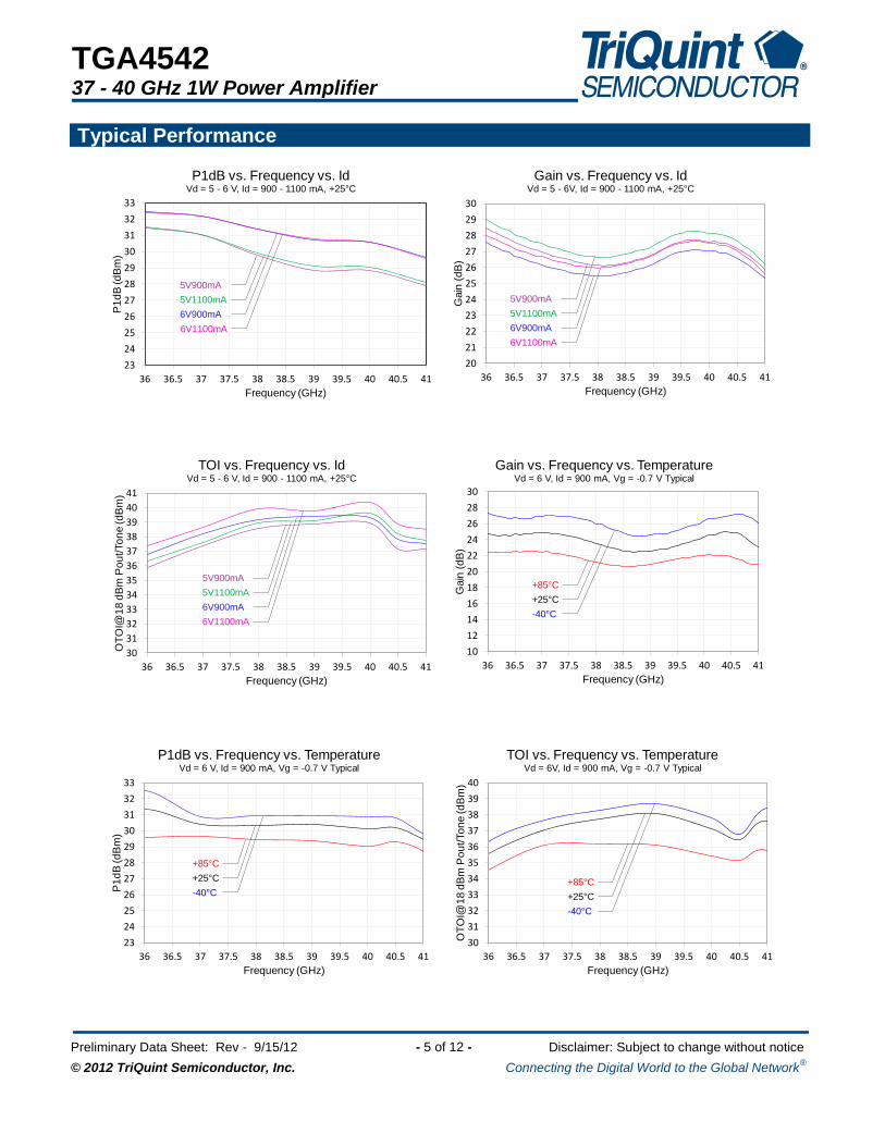
Typical Performance
23
24
25
26
27
28
29
30
31
32
33
36 36.5 37 37.5 38 38.5 39 39.5 40 40.5 41
P1
dB
(d
Bm
)
Frequency (GHz)
P1dB vs. Frequency vs. IdVd = 5 - 6 V, Id = 900 - 1100 mA, +25°C
5V900mA
5V1100mA
6V900mA
6V1100mA
20
21
22
23
24
25
26
27
28
29
30
36 36.5 37 37.5 38 38.5 39 39.5 40 40.5 41
Gain
(d
B)
Frequency (GHz)
Gain vs. Frequency vs. IdVd = 5 - 6V, Id = 900 - 1100 mA, +25°C
5V900mA
5V1100mA
6V900mA
6V1100mA
30
31
32
33
34
35
36
37
38
39
40
41
36 36.5 37 37.5 38 38.5 39 39.5 40 40.5 41
OT
OI@
18
dB
m P
ou
t/To
ne (d
Bm
)
Frequency (GHz)
TOI vs. Frequency vs. IdVd = 5 - 6 V, Id = 900 - 1100 mA, +25°C
5V900mA
5V1100mA
6V900mA
6V1100mA
10
12
14
16
18
20
22
24
26
28
30
36 36.5 37 37.5 38 38.5 39 39.5 40 40.5 41
Gain
(d
B)
Frequency (GHz)
Gain vs. Frequency vs. TemperatureVd = 6 V, Id = 900 mA, Vg = -0.7 V Typical
-40°C
+25°C
+85°C
23
24
25
26
27
28
29
30
31
32
33
36 36.5 37 37.5 38 38.5 39 39.5 40 40.5 41
P1
dB
(d
Bm
)
Frequency (GHz)
P1dB vs. Frequency vs. TemperatureVd = 6 V, Id = 900 mA, Vg = -0.7 V Typical
-40°C
+25°C
+85°C
30
31
32
33
34
35
36
37
38
39
40
36 36.5 37 37.5 38 38.5 39 39.5 40 40.5 41
OT
OI@
18
dB
m P
ou
t/To
ne (d
Bm
)
Frequency (GHz)
TOI vs. Frequency vs. TemperatureVd = 6V, Id = 900 mA, Vg = -0.7 V Typical
-40°C
+25°C
+85°C
TGA4542 37 - 40 GHz 1W Power Amplifier
Preliminary Data Sheet: Rev - 9/15/12 - 6 of 12 - Disclaimer: Subject to change without notice
© 2012 TriQuint Semiconductor, Inc. Connecting the Digital World to the Global Network®
Typical Performance
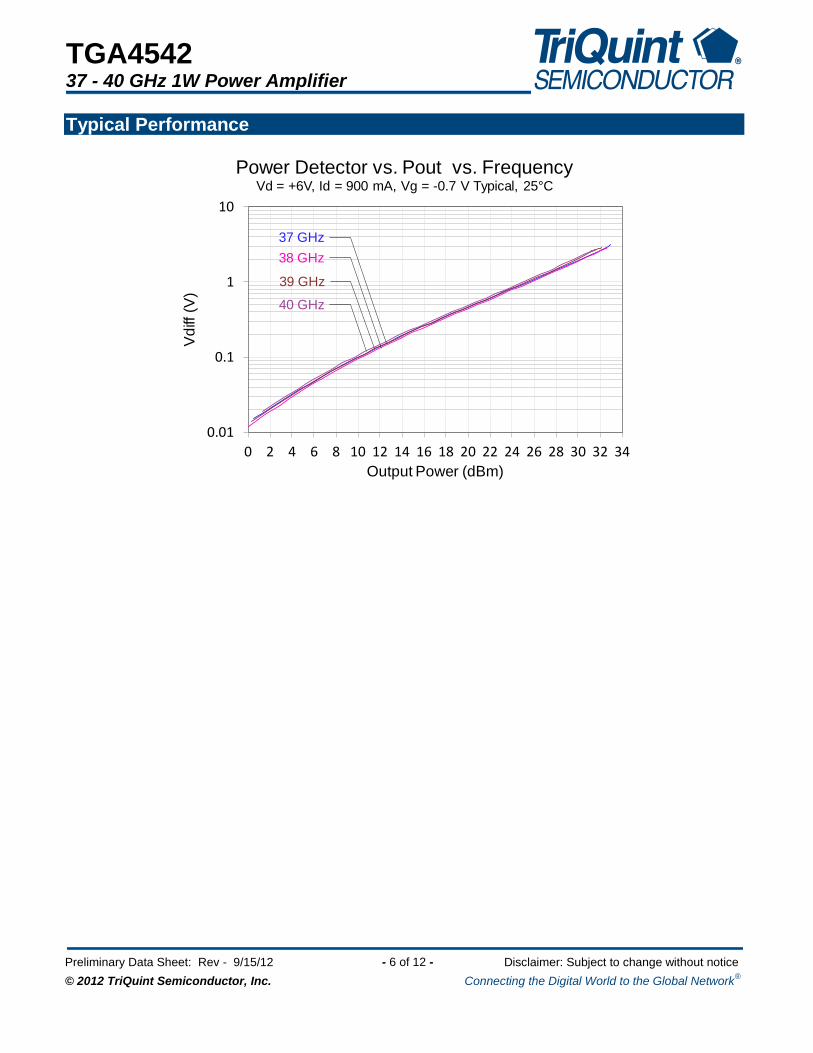
0.01
0.1
1
10
0 2 4 6 8 10 12 14 16 18 20 22 24 26 28 30 32 34
Vd
iff (
V)
Output Power (dBm)
Power Detector vs. Pout vs. FrequencyVd = +6V, Id = 900 mA, Vg = -0.7 V Typical, 25°C
37 GHz
38 GHz
39 GHz
40 GHz
TGA4542 37 - 40 GHz 1W Power Amplifier
Preliminary Data Sheet: Rev - 9/15/12 - 7 of 12 - Disclaimer: Subject to change without notice
© 2012 TriQuint Semiconductor, Inc. Connecting the Digital World to the Global Network®
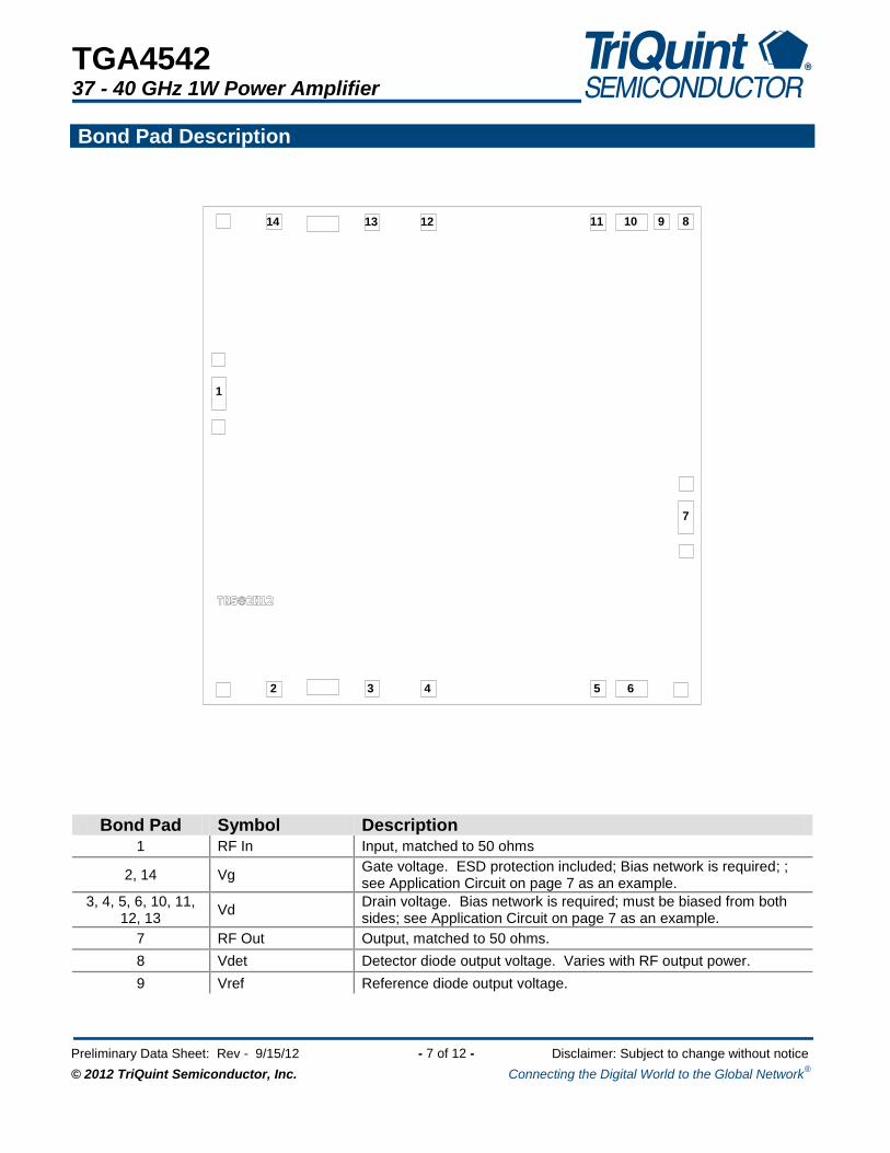
Bond Pad Description
Bond Pad Symbol Description 1 RF In Input, matched to 50 ohms
2, 14 Vg Gate voltage. ESD protection included; Bias network is required; ; see Application Circuit on page 7 as an example.
3, 4, 5, 6, 10, 11, 12, 13
Vd Drain voltage. Bias network is required; must be biased from both sides; see Application Circuit on page 7 as an example.
7 RF Out Output, matched to 50 ohms.
8 Vdet Detector diode output voltage. Varies with RF output power.
9 Vref Reference diode output voltage.
1
2 3 4 5 6
7
891011121314

TGA4542 37 - 40 GHz 1W Power Amplifier
Preliminary Data Sheet: Rev - 9/15/12 - 8 of 12 - Disclaimer: Subject to change without notice
© 2012 TriQuint Semiconductor, Inc. Connecting the Digital World to the Global Network®
Application Circuit
Vd must be biased from both sides. Vg can be biased from either side.
Bias-up Procedure Bias-down Procedure Vg set to -1.5 V Turn off RF supply
Vd set to +6 V Reduce Vg to -1.5V. Ensure Id ~ 0 mA
Adjust Vg more positive until quiescent Id is 900 mA. This will be ~ Vg = -0.7 V
Turn Vd to 0 V
Apply RF signal to RF Input Turn Vg to 0 V
Vref
Id = 900 mA
Vdet
Vdiff
RF OutRF In
11121314
543 62
910
8
71
Vg
-0.7 V Typical
C1
100 pFC7
0.01 uF
C2
100 pF
C3
100 pF
C4
100 pF
C5
100 pF
C6
100 pF
C8
0.01 uF
C9
0.01 uF
C10
0.01 uF
C11
0.01 uFC12
0.01 uF
R1
10 Ohm
C13
1 uF
C14
1 uF
R2
10 Ohm
R3
10 Ohm
C15
1 uF
R5
40k Ohm
R4
40k Ohm
6 V

TGA4542 37 - 40 GHz 1W Power Amplifier
Preliminary Data Sheet: Rev - 9/15/12 - 9 of 12 - Disclaimer: Subject to change without notice
© 2012 TriQuint Semiconductor, Inc. Connecting the Digital World to the Global Network®
Application Circuit
C10
0.01 uF
C11
0.01 uF
C12
0.01 uF
C4
100 pF
C5
100 pF
C6
100 pF
C7
0.01 uF
C8
0.01 uF
C9
0.01 uF
C1
100 pF
C2
100 pF
C3
100 pF
Vg Vd12 Vd34
Vg Vd12 Vd34
Vg = -0.7 V
Typical
Vd = 6 V,
Id = 900 mA
R1
10 Ohm
R2
10 Ohm
C14
1 uF
C15
1 uF
R3
10 Ohm
C13
1 uF
C16
1 uF
R4
10 Ohm
C17
1 uF
R5
10 Ohm
RF In
RF Out
Bill of Material
Ref Des Value Description Manufacturer Part Number
C1, C2, C3, C4, C5, C6 100 pF Cap, 50V, 10%, Single Layer Cap various
C7, C8, C9, C10, C11, C12 0.01 µF Cap, 50V, 10%, SMD various
TGA4542 37 - 40 GHz 1W Power Amplifier
Preliminary Data Sheet: Rev - 9/15/12 - 10 of 12 - Disclaimer: Subject to change without notice
© 2012 TriQuint Semiconductor, Inc. Connecting the Digital World to the Global Network®
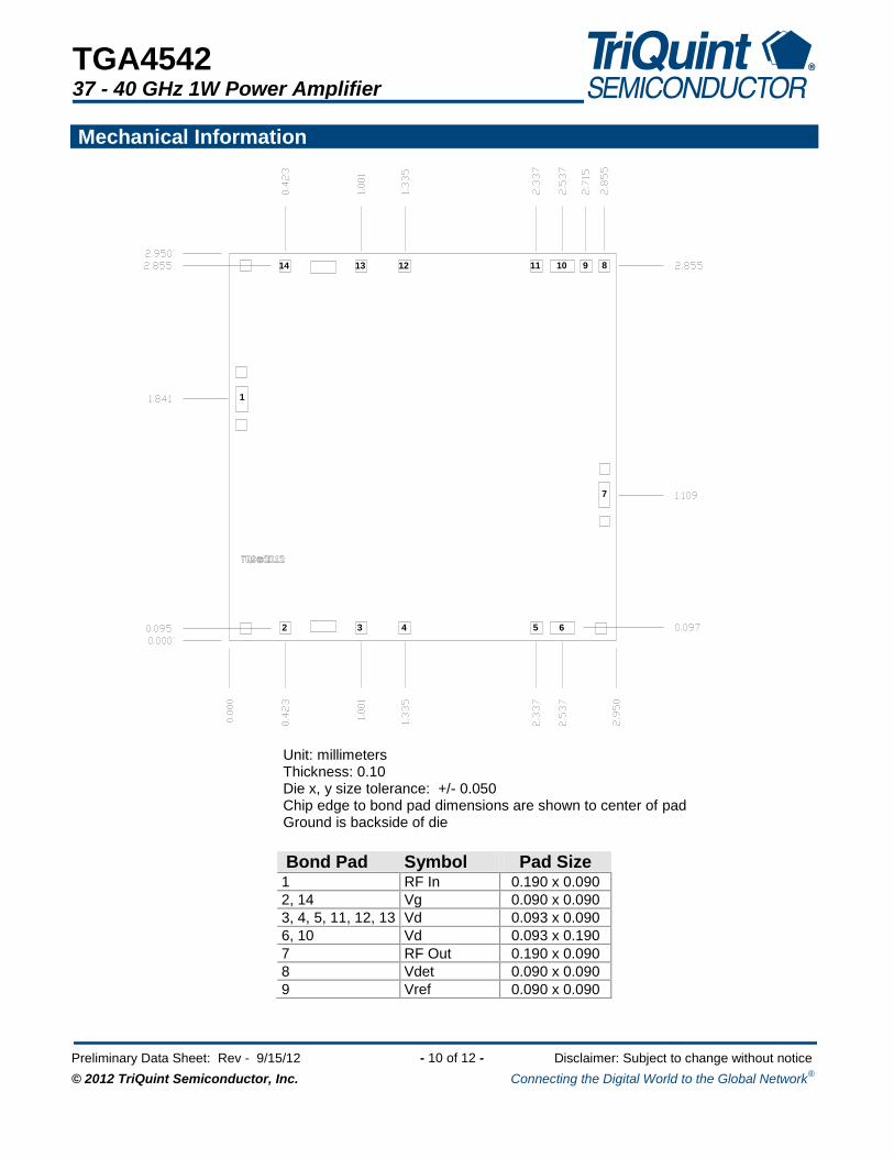
Mechanical Information
Unit: millimeters Thickness: 0.10 Die x, y size tolerance: +/- 0.050 Chip edge to bond pad dimensions are shown to center of pad Ground is backside of die
1
2 3 4 5 6
7
891011121314
Bond Pad Symbol Pad Size 1 RF In 0.190 x 0.090
2, 14 Vg 0.090 x 0.090
3, 4, 5, 11, 12, 13 Vd 0.093 x 0.090
6, 10 Vd 0.093 x 0.190
7 RF Out 0.190 x 0.090
8 Vdet 0.090 x 0.090
9 Vref 0.090 x 0.090

TGA4542 37 - 40 GHz 1W Power Amplifier
Preliminary Data Sheet: Rev - 9/15/12 - 11 of 12 - Disclaimer: Subject to change without notice
© 2012 TriQuint Semiconductor, Inc. Connecting the Digital World to the Global Network®
Product Compliance Information
ESD Information
ESD Rating: Class 0 Value: Passes 100V Test: Human Body Model (HBM) Standard: JEDEC Standard JESD22-A114
Solderability
Compatible with both lead-free (260 °C max. reflow temp.) and tin/lead (245 °C max. reflow temp.) soldering processes.
RoHS Compliance
This part is compliant with EU 2002/95/EC RoHS directive (Restrictions on the Use of Certain Hazardous Substances in Electrical and Electronic Equipment). This product also has the following attributes:
Lead Free
Halogen Free (Chlorine, Bromine)
Antimony Free
TBBP-A (C15H12Br402) Free
PFOS Free
SVHC Free
Assembly Notes
Component placement and adhesive attachment assembly notes: • Vacuum pencils and/or vacuum collets are the preferred method of pick up. • Air bridges must be avoided during placement. • The force impact is critical during auto placement. • Organic attachment (i.e. epoxy) can be used in low-power applications. • Curing should be done in a convection oven; proper exhaust is a safety concern.
Reflow process assembly notes:
• Use AuSn (80/20) solder and limit exposure to temperatures above 300C to 3-4 minutes, maximum.
• An alloy station or conveyor furnace with reducing atmosphere should be used. • Do not use any kind of flux. • Coefficient of thermal expansion matching is critical for long-term reliability. • Devices must be stored in a dry nitrogen atmosphere.
Interconnect process assembly notes:
• Thermosonic ball bonding is the preferred interconnect technique. • Force, time, and ultrasonics are critical parameters. • Aluminum wire should not be used. • Devices with small pad sizes should be bonded with 0.0007-inch wire.

TGA4542 37 - 40 GHz 1W Power Amplifier
Preliminary Data Sheet: Rev - 9/15/12 - 12 of 12 - Disclaimer: Subject to change without notice
© 2012 TriQuint Semiconductor, Inc. Connecting the Digital World to the Global Network®
Contact Information For the latest specifications, additional product information, worldwide sales and distribution locations, and information about TriQuint:
Web: www.triquint.com Tel: +1.972.994.8465 Email: [email protected] Fax: +1.972.994.8504 For technical questions and application information: Email: [email protected]
Important Notice The information contained herein is believed to be reliable. TriQuint makes no warranties regarding the information contained herein. TriQuint assumes no responsibility or liability whatsoever for any of the information contained herein. TriQuint assumes no responsibility or liability whatsoever for the use of the information contained herein. The information contained herein is provided "AS IS, WHERE IS" and with all faults, and the entire risk associated with such information is entirely with the user. All information contained herein is subject to change without notice. Customers should obtain and verify the latest relevant information before placing orders for TriQuint products. The information contained herein or any use of such information does not grant, explicitly or implicitly, to any party any patent rights, licenses, or any other intellectual property rights, whether with regard to such information itself or anything described by such information. TriQuint products are not warranted or authorized for use as critical components in medical, life-saving, or life-sustaining applications, or other applications where a failure would reasonably be expected to cause severe personal injury or death.