Embed Size (px)
Citation preview

Features• Digital combo multi-mode PFC + time-shift LLC resonant half-bridge controller• Management of both AC and DC input• Input voltage range up to 305 VAC• On-board 800 V start-up circuit, line sense• Enhanced fixed-on-time multi-mode TM PFC controller with input voltage feed-
forward, new thd optimizer and frequency limitation• Complete set of PFC protections• Time-shift control of resonant half-bridge• Brownout protection• Complete set of half-bridge protections• S020 package
Application• Street lighting• Home lighting• Industrial
DescriptionThe STNRG012 embodies a multi-mode (Transition-Mode and DCM) PFC controller,a high-voltage double-ended controller for LLC resonant half-bridge, an 800 V-ratedstart-up generator and a sophisticated digital engine that manage optimal operationof three blocks.
The STNRG012 manages both input line AC or DC.
The device comes in a 20-pin SO package and offers an advanced solution forpower-factor-corrected high-efficiency converters supposed to comply with the moststringent energy saving regulations.
The power system and the control algorithms are managed by an 8 bit core withdedicated fast peripherals (SMED). Optimized digital algorithms together with HWanalog IPs are implemented to guarantee very high performance, BOM optimizationand robustness.
The digital algorithms are stored in an internal ROM memory and all key applicationparameters can be stored into a device’s NVM memory during production phase,allowing wide configurability and calibration.
The device can also externally communicate through a 2-pin UART, allowing monitorfunction, black box storing into an external flash and software patch upload from theexternal flash.
Product status link
STNRG012
Product label
Digital combo multi-mode PFC and time-shift LLC resonant controller for AC and DC input line
STNRG012
Datasheet
DS13643 - Rev 1 - February 2021For further information contact your local STMicroelectronics sales office.
www.st.com

1 Block diagram
Figure 1. Block Diagram
STNRG012 Block diagram
DS13643 - Rev 1 page 2/34

2 Pin connection
Figure 2. Pin connection (top view)
STNRG012 Pin connection
DS13643 - Rev 1 page 3/34

3 Absolute maximum ratings and thermal data
Table 1. Absolute maximum ratings
Symbol Pin Parameter Value Unit
VAC VAC Voltage range -1 to 800 V
VBOOT BOOT Floating supply voltage, referred to GND -0.3 to 600 + VCC V
VFGND FGND Half-bridge node voltage -3 up to a value included in the rangeBOOT - VCC and BOOT +0.3 V
dVFGND /dt FGND Floating ground max. slew rate 50 V/ns
VHVG HVG HVG voltage FGND -0.3 to BOOT +0.3 V
VVCC VCC IC supply voltage -0.3 to 19 V
VLVGLVG,
PFC_GDVoltage range -0.3 to VCC V
VVCORE VCORE Voltage range -0.3 to 5.5 V
IPFC_CS,
ILLC_CS,
IPFC_ZCD,
PFC_CS,
LLC_CS,
PFC_ZCD
Clamped source current
(pin voltage: < 0V, self-limited)2 mA
VPFC_CS,
VLLC_CS,
VPFC_ZCD
PFC_CS,
LLC_CS,
PFC_ZCD
Positive voltage range VCORE+0.3 V
VPFC_FB,
VLLC_FB
PFC_FB.
LLC_FBVoltage range -0.3 to VCORE+0.3 V
VRX RX Voltage range -0.3 to VCORE+0.3 V
VTX TX Voltage range -0.3Vto VCORE+0.3 V
Table 2. Thermal data
Symbol Parameter Value Unit
Rth j-amb
Jedec 1s0p
Max. thermal resistance, junction-to-ambient,
Jedec 1s0p120 °C/W
Rth j-amb
Jedec 2s2p
Max. thermal resistance, junction-to-ambient,
Jedec 2s2p65 °C/W
Tj Junction temperature operating range -40 to 150 °C
Tstg Storage temperature -55 to 150 °C
STNRG012 Absolute maximum ratings and thermal data
DS13643 - Rev 1 page 4/34

Figure 3. Dynamic thermal resistance, junction-to-ambient
STNRG012 Absolute maximum ratings and thermal data
DS13643 - Rev 1 page 5/34

4 Detailed block diagram
Figure 4. Detailed block diagram
STNRG012 Detailed block diagram
DS13643 - Rev 1 page 6/34

5 Pin function
Table 3. Pin function detailed description
N. Name Function
1 BOOT
High-side gate-drive floating supply voltage.
The bootstrap capacitor is connected between this pin and FGND.
A fast diode has to be connected from this pin and VCC to guarantee recharge of the bootstrapcapacitor.
2 HVG
High-side gate-drive output.
The driver is capable of 0.5 A source and 0.75 A sink peak current (minimum values) to drive theupper MOSFET of the half-bridge leg.
A resistor internally connected to FGND ensures that the pin is never floating.
3 FGND
High-side gate-drive floating ground.
It is the return path for the high-side gate-drive current.
Lay out carefully the connection of this pin to avoid too large spikes below ground.
4 N.C.High-voltage spacer.
The pin is not internally connected to isolate the high-voltage section and ease compliance withsafety regulations (creepage distance) on the PCB.
5 LVG
Low-side gate-drive output.
The driver is capable of 0.5 A source and 0.75 A sink peak current (minimum values) to drive thelower MOSFET of the half-bridge leg.
The pin is actively pulled to GND during UVLO.
6 TX TX pin for UART/I2C interface
7 RX RX pin for UART/I2C interface
8 LLC_CS
LLC tank current sensing input. A voltage proportional to the tank current (usually obtained with acapacitive divider) has to be applied to this pin.
The information is used for zero-crossing detection (required by time-shift algorithm), the first andsecond level OCP.
9 LLC_AUX LLC_AUX is connected to a divider sensing the auxiliary voltage from the LLC transformer. TheLLC OVP detection is active on this pin.
10 LLC_FB The voltage from this pin is used as the LLC feedback voltage. It has to be connected to thefeedback phototransistor collector and a pull-up resistor to VCORE.
11 PFC_ZCD PFC ZCD input, connected to the PFC AUX winding through a resistor divider detecting the PFCinductor demagnetization.
12 PFC_CS
Current sense input for PFC.
The current flowing in the MOSFET is sensed through a resistor, and the resulting voltage isapplied to this pin.
After GD turns on, a first voltage threshold cross allows enhanced COT control implementation. Asecond level can be detected for overcurrent protection.
13 PFC_FB Input for PFC output voltage. It is used for closing the PFC loop and OVP protection. It has to beconnected with a voltage divider to the bulk capacitor.
14 VCORE Internal VCORE bypass capacitor connection.
15 SGND Signal ground. Reference ground for analog signals.
16 PGNDPower ground. Current return for the PFC gate-driver and the low-side gate-driver of the half-bridge. Keep the PCB trace that goes from this pin to the sources of the PFC and the low-sideMOSFETs separate from the trace that collects the grounding of the bias components.
17 PFC_GD PFC gate-driver output.
STNRG012 Pin function
DS13643 - Rev 1 page 7/34

N. Name FunctionThe output stage is able to drive power MOSFETs, it is capable of 0.7 A source current and 0.8 Asink current (minimum values).
18 VCC
Supply voltage of both the signal part of the IC and the gate-drivers. A bypass capacitor to GNDis necessary to sustain the IC during startup and low power modes.
The voltage on the pin is internally clamped to protect the internal circuits from temporaryexcessive supply voltages.
19 N.C. The pin is not internally connected to isolate the high-voltage section and ease compliance withsafety regulations (creepage distance) on the PCB.
20 VAC
High-voltage startup generator input.
The pin has to be connected directly to the mains voltage through two dedicated diodes. If thevoltage on the pin is higher than 40 V, an internal current source charges the capacitor connectedbetween the pin VCC and GND until the voltage on the VCC pin reaches the startup threshold.
Normally, the generator is re-enabled when the voltage on the VCC pin falls below the UVLOthreshold.
The pin is also used as the line voltage sensing input.
This pin is internally connected to a 20 MΩ resistor divider. It is used for all line sense relatedfunctions: the brownout, input voltage feed-forward, line synchronization.
STNRG012 Pin function
DS13643 - Rev 1 page 8/34

6 Electrical characteristics
(Tj = -40°C to +125°C,Vcc = VBOOT = 15 V,CHVG = CLVG = CGD_PFC = 1 nF; unless otherwise specified)
Table 4. Electrical characteristics
Symbol Parameter Test Condition Min. Typ. Max. Unit
SUPPLY VOLTAGE
Vccz Vcc clamp 19 - -
Vcc Operating range After turn-on 9.5 - 19 V
VccOnProcessing turn-
on threshold Voltage rising(1) 16 17 18 V
VccOffProcessing turn-
off threshold Voltage falling(1) 7.9 8.7 9.4 V
Hys Hysteresis - 8.3 - V
VccCoreOnVCC threshold for
VCore turn-on Voltage rising(1) - 8 - V
VccCoreOffVCC threshold for
VCore turn-off Voltage falling(1) - 7 - V
VCore Operating range Isource 0 to 1 mA 4.75 - 5.25 V
SUPPLY CURRENT
IVCCSQuiescent currentduring sleep (BM) T 25°C - 0.5 - mA
IvCCQ
Operating supplycurrent @ fsw =
50 kHz, C = 1 nF,VCC = 12 V
PFC and LLC off - 18 -
mAPFC driver only (during pfcss) - 20 -
All drivers - 22 -
HIGH-VOLTAGE START-UP GENERATOR
VAC_BRBreakdown
voltageIHV < 50 µA
VCC > VCCOn800 - - V
IVAC_onON-state input
current
VVAC > 40 V
Vcc < 0.8 V- 1 -
mA
VVAC > 40 V
0.8 V < Vcc < VccCoreOn- 6 -
VVAC > 100 V
VccCoreOn < Vcc < 14 V- 6 -
VVAC > 100 V
14 V < Vcc < Vcc_on- 4 -
40 V < VVAC < 100 V
VccCoreOn < Vcc < 14 V- 20 -
40 V < VVAC < 100 V
14 V < Vcc < Vccon- 10 -
Ivcc_chargeON-state VCCcharge current
VVAC > 40 V
Vcc < 0.8 V-0.5 -0.75 -1.3
mAVVAC > 40 V
0.8 V < Vcc < VccCoreOn-3.5 -5 -8
STNRG012 Electrical characteristics
DS13643 - Rev 1 page 9/34

Symbol Parameter Test Condition Min. Typ. Max. Unit
Ivcc_chargeON-state VCCcharge current
VVAC > 100 V
VccCoreOn < Vcc < 14 V
mA
- -5 -
VVAC > 100 V
14 V < Vcc < Vccon- -3.5 -
40 V < VVAC < 100 V
VccCoreOn < Vcc < 14 V- -18 -
40 V < VVAC < 100 V
14 V < Vcc < Vccon- -8 -
IVAC_offOFF-state VAC
input current VVAC = 400 V, Vcc > Vccon - 20 40 µA
IVAC_HV_SINKVAC readingimprovement
currentVVAC = 100 V - 100 - µA
PFC - GATE DRIVER
VOLOutput low
voltage Isink = 100 mA - - 0.7 V
VOHOutput high
voltage
Isource = -10 mA
VCC = 10 V,
VCC = 18 V
9.85
17.9
9.95
17.95
-
-V
IsrcpkPeak source
current Cgate = 4.7 nF(2) -0.7 -1.1 - A
Isnkpk Peak sink current Cgate = 4.7 nF(2) 0.8 1.3 - A
tf Voltage fall time - 25 - ns
tr Voltage rise time - 30 - ns
PFC_uvlo UVLO saturation Vcc = 0 to Vccon, Isink = 1mA - 0.9 1.15 V
LOW-SIDE GATE DRIVER (voltages referred to GND)
VOLOutput low
voltage Isink = 100 mA - - 0.7 V
VOHOutput high
voltage
Isource = 10 mA
Vcc = 10 V
Vcc = 18 V
9.85
17.85
9.9
17.9
-
-V
IsrcpkPeak source
current Cgate = 4.7 nF(2) -0.5 -0.8 - A
Isnkpk Peak sink current Cgate = 4.7nF(2) 0.75 1.2 - A
tf Voltage fall time - 25 - ns
tr Voltage rise time - 40 - ns
LVG_uvlo UVLO saturation Vcc = 0 to Vccon, Isink = 1mA - 0.9 1.15 V
HIGH-SIDE GATE DRIVER (voltages referred to FGND)
VOLOutput low
voltage Isink = 100 mA - - 0.7 V
VOHOutput high
voltage
Isource = 10 mA
VBOOT = 10 V,
VBOOT = 18 V
9.85
17.85
9.9
17.9
-
-V
STNRG012 Electrical characteristics
DS13643 - Rev 1 page 10/34

Symbol Parameter Test Condition Min. Typ. Max. Unit
IsrcpkPeak source
current Cgate = 4.7nF(2) -0.5 -0.8 - A
Isnkpk Peak sink current Cgate = 4.7nF(2) 0.75 1.2 - A
tf Voltage fall time - 25 - ns
tr Voltage rise time - 40 - ns
HSGD_pdwHSGD-COMM
pull-down - 25 - kΩ
IFGNDCurrent from
VBOOT to FGND Vboot= 200 V - 1.5 - µA
BROWN IN/OUT
BI(3)
THVline rising 112 114 116 V
BO(3) Vline falling 108 V
BIBO_H(3) Hyst 5.25 6 6.75 V
BO_mask Brownout time 77 ms
Overtemperature (by design)
OTP_TH TH T rising 130 140 150 C
OTP_H Hyst T rising -30 C
CK
Fck Ck run mode 57 60 63.7 MHz
ADC
ADC_res Resolution Vin ADC > 50 mv - 10 - bit
FSR Conversion range 0 - 2.5 V
DNL Differential nonlinearity Vin ADC > 50 mv - ±1.5 - lsb
Fck_adc Clock frequency Vin ADC > 50 mv - 15 - MHz
Ts Sampling time Vin ADC > 50 mv - 7 - Adc Ckcycles
TcTotal conversiontime (sampling
included)Vin ADC > 50 mv - 18 - Adc Ck
cycles
COMPARATORS
PFC_CSRECOT(4)
TH RISE (DAC6bit)
Input pin PFC_CS
FSR = 125
STEP = 1.95 mV
HYST 5
PFC_CS OC1TH RISE
Input pin PFC_CS500
mVTH FALL 450
PFC_CS OC2TH RISE
Input pin PFC_CS900
mVTH FALL 850
PFCZCD ZCD(4)
TH FALLING(TH_F)
Input pin PFC_ZCD
0/50/100/200
mVHYST (TH_R)
210/110(5)/310/
TH_F +10
PFC_FB OVPTH RISING
Input pin PFC_FB2.33 V
HSYR 75 mV
LLC_FB(4)
BURST
TH RISINGInput pin LLC_FB
0.75/1/1.25 V
HYST 5/10 mV
STNRG012 Electrical characteristics
DS13643 - Rev 1 page 11/34

Symbol Parameter Test Condition Min. Typ. Max. Unit
LLC_FB
SHUTDOWN
TH RISINGInput pin LLC_FB
145mV
TH FALLING 125
LLC_AUX OVPTH RISE
Input pin LLC_AUX2.5
VTH FALL 2.4
LLC_AUX ExtBM.
TH RISINGInput pin LLC_AUX
0.9V
TH FALLING 0.8
LINE SURGETH RISING
Input pin VAC430
VTH FALLING 410
LLC_OC1(4)
TH RISING (DAC5bit) Input pin LLC_CS
FSR = 500
STEP = 15.6mV
HYST 20
mVLLC_OCP2
TH RISINGInput pin LLC_CS
700
TH FALLING 650
1. Parameters tracking each other.2. Guaranteed by design, not production tested.3. Thresholds referred only to AC input line.4. Thresholds and hysteresis are programmed by the software in use.5. The selection for TH_R = 110 mV is not allowed if TH_F = 200 mV.
STNRG012 Electrical characteristics
DS13643 - Rev 1 page 12/34

7 Typical application schematic
Figure 5. Typical application schematic (part 1)
STNRG012 Typical application schematic
DS13643 - Rev 1 page 13/34
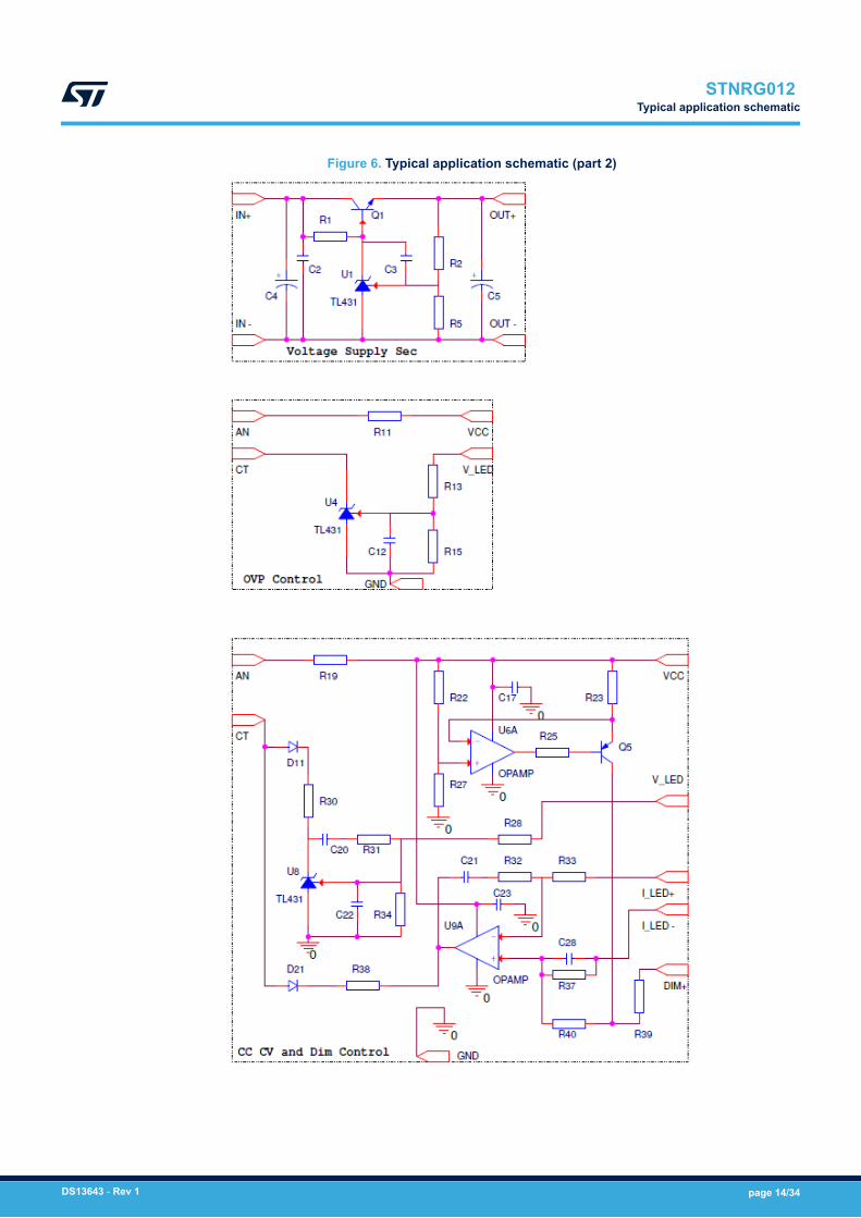
Figure 6. Typical application schematic (part 2)
STNRG012 Typical application schematic
DS13643 - Rev 1 page 14/34

8 Architecture
The PFC and LLC external MOSFETs gates are managed by the “State Machine Event Driven” (SMEDs): 2 forPFC (PFC SMEDs) and 2 for LLC (LLC SMEDs).The SMEDs are programmable state machine driven by events:1. External events2. Analog comparators outputs3. Power manager generated events (protections)4. Internal events5. Timers eventsPFC SMEDs• Inputs events: PFC RECOT, PFC OC1, PFC ZCD• Outputs: PFC_GD
LLC SMEDs• Inputs events: LLC ZCD• Outputs: LVG, HVG
The μP subsystem manages dynamically the control loop.• Analog comparators thresholds setting• SMED configuration• SMED timers• ADC scheduler• Interrupt management
The multichannel ADC is controlled by a programmable event driven scheduler: sampling sequence can beconfigured and every sample can be triggered by a specific SMED state occurrence and an internal timer value.Different priorities can be programmed to allow fast sampling for real time control and slow sampling for statecontrol.The scheduler can be programmed to generate interrupts after completion of selectable conversions.A dedicated AC line monitor easily follows the AC line providing system triggers.The uP reads data from the ADC and performs the loop calculation with the support of a dedicated 16-b x 16-bmultiplier and a 32-b accumulator unit.A Power management and burst-mode machine manages the system power state in order to have very lowidle consumption and fast activity restart during the burst-mode operation.Hard protections are managed with a very low propagation delay; the protection enable and the latched/notlatched response are programmable. If not specified, the duration of autorestart timer for not latched response isconfigurable by one NVM parameter.The power manager controls also the brown-in/out, VCC charge/discharge and AC monitor.A Watchdog resets the system in case of missed µP signal for a long time.A communication peripheral allows serial communication at startup and during the normal operation for:• External memory communication for
– Black box external recording– Patch SW upload
• Monitoring• Internal memory R/W and NVM management• Test mode
STNRG012 Architecture
DS13643 - Rev 1 page 15/34

9 Functional description
The main functions are:• HV startup and VCC management• Line monitor and protection• Drivers• PFC control and fault management• Resonant HB control and fault management• Power management• Communication and configuration
9.1 HV startup and VCC managementThe VAC pin voltage can be both:• a rectified sine wave at 100 Hz/120 Hz• a DC voltage
The VAC pin is the device supply at the startup.At the VAC pin a HV DMOS is internally connected to charge the capacitor connected to the VCC pin.From the VCC pin an internal LDO provides the 5 V VCore for analog and digital circuitry; the digital section issupplied by the internal LDO from the VCORE pin.At startup, from the HV DMOS the capacitor connected to the VCC pin is charged to provide the power supply tothe whole device; then the HV DMOS is turned off.The VCC pin starts sourcing current to the connected capacitor after about 15 V VAC pin voltage.The VCC capacitor charge current is limited to 0.75 mA (typ.) during the first charge phase to limit thetemperature increase in case the VCC pin is short-circuited at startup. After the VCC pin voltage is above 0.8 V,the charging current rises to 5 mA (typ.).VCORE pin voltage rises when the VCC pin crosses 8 V (VccCoreOn). There is a VCORE overload protection thatlimits the VCC charging current below 1.3 mA in case the VCORE pin is short-circuited at startup. Then the VCCcapacitor charge continues with an average current higher than 6 mA: the current is increased during the time theVAC pin voltage is below 100 V (see Electrical characteristics table, parameter Ivcc_charge).Once the VCC pin crosses the 17 V, VccOn rising threshold the HV DMOS turns off and the whole device startsworking: the uP boots.If the VCC pin goes below the 8.7 V, VccOff falling threshold (UVLO threshold) the uP stops working and the HVDMOS turns on again.If the VCC pin falls below 7 V (VccCoreOff) the device stops working and the capacitor connected to the VCOREpin discharges. The VCC pin can rise again only after the voltage on the VCORE pin falls below 1 V.The worst case average charging current from the 0.8 V to the Vccon threshold is estimated in 4.6 mA (in case themains voltage is 115 Vac - 60 Hz) and 4.1 mA (in case the mains voltage is 230 Vac - 50 Hz).
9.2 AC line monitor and protectionA HV voltage divider is internally connected to the VAC pin to generate Vline_sense for the input line monitoringand protection:• Brown-in/out• Line synchronization• Line monitor for PFC control
9.2.1 Brown in/outBrown-in and brownout functions are implemented based on the Vline_sense information.
STNRG012 Functional description
DS13643 - Rev 1 page 16/34

The peak, in case of VAC voltage, or its value, in case of VDC voltage, is monitored to enable and disable thePFC. The PFC is enabled when the input pin voltage crosses the brown-in threshold. The PFC is disabled after77 ms (typ.) the VAC pin has gone below the brownout threshold.Please consider that the brownout threshold and hysteresis values are guaranteed for AC input only.In order to improve AC line reading and avoid false brown-in, the HV DMOS is turned on sinking IXCD currentfor 3 ms in case of brownout. In case the device turns off for brownout, only after 100 ms are the turning-onconditions checked again.This function can be enabled / disabled through the dedicated NVM bit.
9.2.2 Line synchronizationA dedicated digital peripheral manages the PFC synchronization with the AC line sine wave.In order to improve AC line reading and synchronization, the HV DMOS is turned on sinking IVAC_HV_SINKcurrent at startup. This function can be enabled / disabled through the dedicated NVM bit.In case the input line switches from AC to DC the device simulates the line synchronization maintaining the ACinput line frequency.In case the input line is DC voltage at the startup, the device emulates the line synchronization as 60 Hz input line(i.e. half period of about 8.3 ms).
9.2.3 Line monitor for PFC controlA 20 MΩ voltage divider for the AC line monitor is internally connected from the VAC pin to GND.
9.2.4 Vline surge stopA surge can be detected on the VAC pin (430 V).During the surge the PFC activity is stopped for one half-cycle.If a line surge is detected during the PFC soft-start, the system shuts down with a not latched fault.The surge protection can be enabled / disabled through the dedicated NVM bit.
9.3 Gate driversThe HVG and LVG are matched drivers. Deadtimes are programmable by the user.During the burst-mode sleep phase, the HS BOOT capacitor discharges. The burst packets always start with anLVG pulse to recharge the bootstrap capacitor. A fast external bootstrap diode is necessary.
9.4 PFC control and fault management
9.4.1 PFC resources
Table 5. PFC related pins
Pin name Description Level Function
PFC_CS PFC MOSFET current sense
0-125 mV 6-bit ramp enhancedCOT feature
500 mV OCP1
900 mV OCP2 Fault
PFC_ZCD PFC auxiliary connection for ZCD detection
PFC_FB Reading for PFC Vout estimation ADC, 10 bit
VAC Mains line voltage reading ADC, 10 bit
PFC_GD PFC MOSFET gate driver
STNRG012 Gate drivers
DS13643 - Rev 1 page 17/34

9.4.2 Vin readingInput line voltage peak (Vin) reading on the VAC pin by the ADC at the AC line peak.In case a DC is applied, the Vin is read each 8.3 ms if the device starts with a DC input. Otherwise, the samplingperiod depends on the last AC applied before switching to DC.
9.4.3 PFC output voltage feedback readingPFC output voltage reading on the PFC_FB pin by the ADC.
9.4.4 PFC OVP comparatorThe PFC OVP comparator sets the limit for the PFC output voltage.It monitors the PFC_FB pin with respect to a fixed 2.33 V threshold.
9.4.5 PFC RECOT comparatorThe PFC RECOT comparator implements the TON adjustment for the ramp enhanced constant on-time (RECOT)control.It monitors the PFC_CS pin with respect to a programmable threshold. Its output communicates to the PFCSMED.The new THD optimizer is based on this comparator.
9.4.6 PFC OC1 comparatorThe PFC OC1 comparator sets the limit for the operational maximum allowed peak current into the PFCMOSFET. If the OC1 threshold is hit the PFC_GD is turned off. This protection works cycle by cycle. It monitorsthe PFC_CS pin with respect to a fixed 500 mV threshold. Its output communicates to the PFC SMED.
9.4.7 PFC OC2 comparatorThe PFC OC2 comparator sets a HW limit for the current flowing into the PFC MOSFET: it triggers the OCP fault.It monitors the PFC_CS pin with respect to a fixed 900 mV threshold.
9.4.8 PFC ZCDThe PFC ZCD comparator performs the zero cross detection to implement the soft switching of the PFCMOSFET.It monitors the PFC_ZCD pin with respect to two programmable rising and falling thresholds.Its output communicates to the PFC SMED.Please consider that the PFC ZCD feedback disconnection is not implemented.
9.4.9 PFC state machine event driven (SMED)The PFC high frequency operations are managed by a programmable 8-state ”State Machine Event Driven” (2coupled 4-state SMEDs).The SMED controls the PFC MOSFET based on the PFC comparators output and internally controlled counters.It generates also the comparators' enable signals. It works at 60 MHz.
9.5 PFC algorithmThe PFC operates based on a multi-mode scheme.A constant on-time (COT) control is implemented; TON is calculated from the PFC feedback and the measuredVin (the peak in case of a VAC, its value in case of a VDC).TON is calculated and updated at the line cycle valley in case of VAC input, otherwise the system executes theTON calculation each 8.3 ms (in case the device starts with DC input).Based on the working PFC's operating state variables, the working mode is changed to optimize the overallefficiency.
STNRG012 PFC algorithm
DS13643 - Rev 1 page 18/34

The device includes an automatic bulk voltage drop management: during running operation, in case the PFC_FBpin is below 31 LSB with respect to the target, the device boosts the PFC output changing automatically thecontrol loop parameters (only during the management of the drop).
9.5.1 Ramp enhanced COT improved (patented)The PFC control is based on the constant on-time scheme, with a proprietary improved algorithm: the calculatedTON is applied only after the PFC RECOT comparator is triggered to balance the recovery diode energy and theEMI capacitor current.The PFC RECOT comparator threshold is adjusted by the core with a 6-bit DAC and allows to apply theprogrammed base and ramp (defined by user into NVM).This feature allows improving the total harmonic distortion (THD) and the power factor (PF) of the application.
9.5.2 New THD optimizer (patented)The device implements the new THD optimizer algorithm that can be enabled/disabled by the NVM. This new(patented) algorithm is based on the enhanced COT:The PFC RECOT comparator threshold is adjusted by the core with a 6-bit DAC but, instead of constantthreshold, the DAC value depends on both the phase of the AC input line and on the mode of the PFC.
Figure 7. New THD optimizer algorithm example
The user can fine tune the algorithms by the related NVM parameters.
9.5.3 Operating modesThe PFC manager changes the operating modes by dynamically reconfiguring the SMEDs, obtaining optimalperformances in terms of both efficiency and THD/PF.• Transition mode (TM mode)• Valley skipping• Discontinuous mode (DCM)
9.6 PFC protections
9.6.1 PFC OVPThe device includes two different PFC OVP protections: hardware (based on PFC_OVP comparator) andsoftware (based on ADC PFC_FB sampling). In both cases, if the PFC OVP protection is triggered during therunning state of the PFC, the device turns off the PFC until the next line valley. The HW OVP threshold is fixed,the SW OVP threshold is an NVM parameter.Please see the PFC_CS disconnection paragraph for information about PFC_OVP and PFC_CS disconnection.The device shuts down for PFC_OVP only if all the following three conditions are triggered:• the PFC_OVP HW comparator is triggered during the PFC startup• the feedback disconnection faults are enabled• PFC_CS comparator is not triggered during PFC start-up phase
STNRG012 PFC protections
DS13643 - Rev 1 page 19/34

Please consider that in all other cases the device does not enter fault state so the half-bridge input voltage couldbe higher than the PFC_OVP HW threshold with the output still in regulation.
9.6.2 PFC OCP2If the PFC OC2 comparator is triggered, the PFC gate is truncated and remains off until the beginning of anew line half cycle. In case the PFC OC2 comparator is triggered for more than a programmable number ofconsecutive half line cycles, the device enters the OCP2 fault and it is turned off.The OCP2 fault can be programmed as latched or not latched.
9.6.3 PFC soft-start timeoutIf the PFC soft-start is not finished after 1 s the system enters the PFC soft-start timeout fault state and it is turnedoff. The fault is not latched.
9.6.4 PFC UVPIf the PFC_FB pin is below a programmable threshold for more than about 600 us, the device enters the PFCUVP fault and it shuts down. The PFC UVP fault is a not latched fault.In case the LLC is in running state and the PFC UVP is triggered, the not latched timer depends on the relatedNVM parameter and could be set to either:• 100 ms
or• Programmable autorestart timer for not latched fault
In case the PFC UVP is triggered and the LLC is not in running state (i.e. soft-start or ACP management state),the duration of not latched timer is set to the programmable autorestart timer for not latched fault.
9.6.5 PFC_FB disconnectionIt could be enabled/disabled by NVM parameter.If the PFC_FB is stuck low the system enters the PFC_FB disconnection fault state (latched) and it is turned off.
9.6.6 PFC_CS disconnectionIt could be enabled/disabled by NVM parameter. If enabled, the PFC_CS disconnection fault protection is latched.In case the PFC_CS is stuck high during the operative mode, the device enters the PFC_CS disconnectionprotection and it is turned off.In case the PFC_CS pin is stuck low (or high) during the PFC start-up phase, the device enters the PFC_CSdisconnection protection and it is turned off.In particular, during the start-up phase if the disconnection faults detection is enabled and the PFC_OVP istriggered, the device behavior depends on the following cases:• If the voltage of PFC_FB pin is between PFC_FB target and HW PFC_OVP threshold:
– AC CASE: as long as the PFC_CS is not triggered, after the 45° input line phase, the system turns onthe PFC gate for a few pulses about every 0.6 ms.
– DC CASE: if the PFC_CS is not triggered the system turns on the PFC gate for a few pulses beforeentering the soft-start phase.
in both cases, if the PFC_CS comparator is not triggered during the start-up phase and the feedbackdisconnections are enabled, the device turns off entering PFC_CS disconnection fault protection.• If the voltage of PFC_FB pin is above the HW PFC_OVP threshold:
– in case the PFC_CS is not triggered the device turns off entering PFC_OVP fault protection (notlatched).
STNRG012 PFC protections
DS13643 - Rev 1 page 20/34

9.7 LLC control and protection
9.7.1 LLC related resources
Table 6. LLC related pins
Pin name Description Level Function
LLC_CS Low-side current sense0-500 mV 5 bit OLP
700 mV OCP2 fault
LLC_AUX LLC auxiliary winding voltage sense0.9 V External burst mode
2.5 V LLC output OVP
LLC_FB LLC OPTO feedback sense, burstcomparator and SHUTDOWN comparator
ADC, 10 bit Feedback sense
Programmable Burst comparator
125 mV Shutdown comparator
HVG High-side gate driving
LVG Low-side gate driving
9.7.2 LLC OC1 comparatorThe LLC OC1 comparator implements the overload protection (OLP). It monitors the LLC_CS pin with respect toa programmable threshold. If the LLC_CS pin goes every cycle over the OC1 threshold for a programmable time,the IC shuts down and enters the OLP fault.Both threshold and duration are programmable trough NVM parameters.
9.7.3 LLC OC2 comparatorThe LLC OC2 comparator sets a HW limit for the current flowing into the LLC resonant tank: it triggers the OCP2fault.It monitors the LLC_CS pin with respect to a fixed 700 mV threshold. If this threshold is triggered for aprogrammable consecutive number of cycles, the OCP2 fault is triggered and the system shuts down.
9.7.4 LLC ZCD comparatorThe LLC ZCD comparator detects the LLC current zero-crossing during the normal operation to implement thetime-shift control and the anti-capacitive protection.Its output communicates to the LLC SMED.The comparator’s hysteresis is programmable by NVM choosing between the available values 5 mV or 10 mV. Itis recommended to use the 10 mV hysteresis.
9.7.5 LLC_FB voltage reading: OPTO feedback loop errorThe LLC_FB pin is connected to the optocoupler and its voltage is the error signal of the LLC loop.The LLC_FB voltage is sampled by the ADC to calculate the time-shift.
9.7.6 Shutdown featureIf the LLC_FB pin is forced below 125 mV, the device shuts down. If the voltage returns over such threshold thesystem restarts performing the soft-start.This feature can be enabled / disabled using an NVM bit.
9.7.7 SMEDsHVG and LVG are driven by an event driven 60 MHz state machine (2 coupled 4-state SMEDs).Driving events are the ZCD event and the elapsing of the programmable time which sets the high-side andlow-side time-shift values and drivers deadtime.
STNRG012 LLC control and protection
DS13643 - Rev 1 page 21/34

9.7.8 AlgorithmThe LLC operation is based on “Symmetric Time-Shift Control” (STSC), an improved version of time-shift controlthat guarantees 50% of the HB duty cycle. The time-shift value is calculated from the LLC_FB pin.
9.7.9 Time-shift (patented)The TSC methodology consists in controlling the amount of time elapsing from a zero crossing of the tank currentto the switch-off of the MOSFET currently on.Conceptually, with TSC an inner loop is closed and the outer loop that regulates the output voltage provides thereference for the inner loop. This inner loop is completely managed by SMEDs using the zero current detectioninformation.
9.8 LLC protections
9.8.1 Anti-capacitive protectionAnti-capacitive control is applied at the SMEDs level using ZCD time events.The IC monitors the phase relationship between the LLC tank current sensed on the LLC_CS pin and the voltageat the HVG and LVG, checking the time between the gate rising edge and the tank current zero cross detection.If this time is below a programmable threshold, which is indicative of impending capacitive-mode operation,the monitoring circuit activates the “Soft” ACP procedure: the time-shift is reduced (and therefore the switchingfrequency is increased) in order to keep the converter away from that dangerous condition.If the time reaches “zero” the device is stopped immediately. This is called “Hard” ACP.Both hard and soft ACP can be enabled and disabled through NVM.
9.8.2 LLC OLPIf the LLC OC1 comparator is triggered the system could enter the overload protection (OLP). During this phasethe system regulates the output and checks for a programmable time if the OCP1 event is still present, in thiscase the device is shut down entering the OLP fault state that can be programmed as latched or not latched.
9.8.3 LLC OCP2If the LLC OC2 comparator is triggered for a number of times greater than a threshold set by the user, the devicesets the OCP2 fault and it is shut down. The OCP2 fault can be programmed as latched or not latched.
9.8.4 LLC soft-start timeoutIf the LLC output voltage cannot reach the regulation value within 100 ms, the device enters the LLC soft-starttimeout fault and it is shut down. The fault can be programmed as latched or not latched.
9.8.5 LLC OVPIf the LLC_AUX pin voltage is higher than the LLC OVP comparator threshold (2.5 V) the system enters the LLCOVP fault state and it is turned off. The fault can be programmed as latched or not latched and can be disabled.The autorestart timer is set to about 34 ms in case not latched chosen.
9.8.6 LLC_CS disconnectionIf the LLC_CS pin is stuck at 0 V or 5 V during the soft-start the system enters the LLC_CS disconnection fault(not latched) and it is shut down if the disconnection faults detection is enabled in NVM.
9.8.7 LLC_AUX disconnectionIf the pure external burst-mode is enabled and the LLC_AUX pin is stuck at 0 V during the burst and theLLC_FB pin is higher than the burst comparator threshold, after 32 burst packets the system enters LLC_AUXdisconnection protection (latched) and it is shut down if the disconnection faults detection is enabled in NVM.
STNRG012 LLC protections
DS13643 - Rev 1 page 22/34

9.9 ADCThe system ADC is an 8-channel 15-MHz SAR 10-bit A/D converter.It needs 7 cycles (470 ns) for sampling and 11 cycles (740 ns) to convert the data.It is controlled by an SW programmable scheduler allowing flexible system signals reading:• Fixed time sequence conversion• Event driven sequence conversion
Table 7. ADC input signals
Signal Pin Internal voltage divider FST
Input line voltage VAC Internal voltage divider 484.5 V
PFC feedback voltage PFC_FB Direct reading 2.5 V
LLC feedback voltage LLC_FB Direct reading 2.5 V
9.10 Burst-mode
9.10.1 Specific resourcesBurst comparator on LLC_FB pinThe LLC BURST comparator at the LLC_FB pin is used to wake up the system, in order to perform a burstsequence.The comparator is alive also during sleep and the wake-up threshold is programmable (0.75 V, 1 V, 1.25 V).External burst-mode comparator on LLC_AUX pinThe external burst-mode comparator with the 0.9 V threshold on the LLC_AUX pin is used to enter / exit theburst-mode using an external digital signal. The external burst-mode operation can be enabled / disabled using aNVM bit.30-kHz system oscillatorA 30-kHz oscillator (always on) keeps the system alive.
9.10.2 AlgorithmThe system can manage the deep sleep state with very low VCC current consumption (500 µA).The system in deep sleep• Monitors the AC line for brownout condition• Monitors the burst comparator to detect wake condition• Monitors the VCC for data integrity• Maintains all RAM data
The device implements two different burst-mode algorithms: the LLC_FB burst or external burst. The first one isbased on just the LLC_FB pin voltage, the second one is based on the external BM comparator on the LLC_AUXpin that can be driven sensing the output current.The burst-mode can be programmed to depend either on the LLC_FB pin only, or LLC_AUX pin only, or both. Thisthird possibility is called hybrid external burst.In case of the LLC_FB burst-mode, the device enters sleep mode if the LLC_FB pin voltage goes below aprogrammable threshold. The burst switching activity is enabled after the burst comparator is triggered.The normal switching activity is restored if the time between two bursts is lower than a programmable threshold.This time defines a precise power level at which the controller exits the burst-mode. In order to have a fasterresponse to the big load transient the system exits burst-mode also if the LLC_FB pin voltage is still above theburst comparator threshold after one burst packet.In case of the LLC_AUX pin driven burst-mode, two types of external burst mode could bedefined:• Pure external burst-mode: only the external BM comparator manages the burst-mode entering / exiting;
STNRG012 ADC
DS13643 - Rev 1 page 23/34

• Hybrid external burst-mode: if the external BM comparator is high, the system stays out of burst-mode whileif the external BM comparator is low, burst-mode entering / exiting is managed by the LLC_FB pin settings.
In both external burst-mode cases, the burst switching activity is anyway managed by the LLC_FB pin and theburst comparator.The PFC and LLC switching activities during the burst-mode are synchronized.The LLC can perform a burst without the PFC, depending on the system conditions.
9.11 Communication and configurationThe device communicates with an external digital device through a serial interface.The serial interface uses two dedicated pins with a standard UART protocol. It implements also an I2C protocol forexternal E2PROM writing and reading.The serial interface allows the user• To write the NVM to configure the device in a specific application: 24 bytes are available• To write into the RAM for test and SW patch purposes• To read the NVM content• To read the RAM content• To read registers content• To configure the device for specific tests
Based on a specific code into the NVM the serial interface functionality can be reduced for security reasons.
9.11.1 MonitorSome internal data can be provided to an external digital device through the UART interface for monitoringpurposes.
9.11.2 Black boxBlack box data are written into the external E2PROM (if present) during the normal operation.
9.11.3 PatchesSW patches (if necessary) are uploaded by the device from the external E2PROM at the startup. It can beenabled/disabled using a NVM bit for security reasons.
STNRG012 Communication and configuration
DS13643 - Rev 1 page 24/34

10 Package information
In order to meet environmental requirements, ST offers these devices in different grades of ECOPACK®packages, depending on their level of environmental compliance. ECOPACK specifications, grade definitionsand product status are available at: www.st.com. ECOPACK is an ST trademark.
10.1 SO20 package information
Figure 8. SO20 package outline
Table 8. SO20 package mechanical data
Symbol
Dimension
mm Inch
Min. Typ. Max Min. Typ. Max.
A 2.35 - 2.65 0.093 - 0.104
A1 0.10 - 0.30 0.004 - 0.012
B 0.33 - 0.51 0.013 - 0.020
C 0.23 - 0.32 0.090 - 0.013
STNRG012 Package information
DS13643 - Rev 1 page 25/34

Symbol
Dimension
mm Inch
Min. Typ. Max Min. Typ. Max.
D 12.60 - 13.00 0.496 - 0.512
E 7.40 - 7.60 0.291 - 0.299
e - 1.27 - - 0.050 -
H 10.00 - 10.65 0.394 - 0.419
h 0.25 - 0.75 0.010 - 0.030
L 0.40 - 1.27 0.016 - 0.050
K 0° (min.), 8° (max.)
STNRG012 SO20 package information
DS13643 - Rev 1 page 26/34

11 Ordering information
Table 9. Order codes
Part number Package Packing
STNRG012 SO20 Tube
STNRG012TR SO20 Tape and reel
STNRG012 Ordering information
DS13643 - Rev 1 page 27/34

Revision history
Table 10. Document revision history
Date Version Changes
23-Feb-2021 1 Initial release.
STNRG012
DS13643 - Rev 1 page 28/34

Contents
1 Block diagram . . . . . . . . . . . . . . . . . . . . . . . . . . . . . . . . . . . . . . . . . . . . . . . . . . . . . . . . . . . . . . . . . . . . .2
2 Pin connection . . . . . . . . . . . . . . . . . . . . . . . . . . . . . . . . . . . . . . . . . . . . . . . . . . . . . . . . . . . . . . . . . . . .3
3 Absolute maximum ratings and thermal data . . . . . . . . . . . . . . . . . . . . . . . . . . . . . . . . . . . . . . .4
4 Detailed block diagram . . . . . . . . . . . . . . . . . . . . . . . . . . . . . . . . . . . . . . . . . . . . . . . . . . . . . . . . . . . .6
5 Pin function . . . . . . . . . . . . . . . . . . . . . . . . . . . . . . . . . . . . . . . . . . . . . . . . . . . . . . . . . . . . . . . . . . . . . . .7
6 Electrical characteristics. . . . . . . . . . . . . . . . . . . . . . . . . . . . . . . . . . . . . . . . . . . . . . . . . . . . . . . . . . .9
7 Typical application schematic. . . . . . . . . . . . . . . . . . . . . . . . . . . . . . . . . . . . . . . . . . . . . . . . . . . . .13
8 Architecture . . . . . . . . . . . . . . . . . . . . . . . . . . . . . . . . . . . . . . . . . . . . . . . . . . . . . . . . . . . . . . . . . . . . . .15
9 Functional description . . . . . . . . . . . . . . . . . . . . . . . . . . . . . . . . . . . . . . . . . . . . . . . . . . . . . . . . . . . .16
9.1 HV startup and VCC management . . . . . . . . . . . . . . . . . . . . . . . . . . . . . . . . . . . . . . . . . . . . . . . 16
9.2 AC line monitor and protection . . . . . . . . . . . . . . . . . . . . . . . . . . . . . . . . . . . . . . . . . . . . . . . . . . 16
9.2.1 Brown in/out . . . . . . . . . . . . . . . . . . . . . . . . . . . . . . . . . . . . . . . . . . . . . . . . . . . . . . . . . . . 16
9.2.2 Line synchronization . . . . . . . . . . . . . . . . . . . . . . . . . . . . . . . . . . . . . . . . . . . . . . . . . . . . . 17
9.2.3 Line monitor for PFC control . . . . . . . . . . . . . . . . . . . . . . . . . . . . . . . . . . . . . . . . . . . . . . . 17
9.2.4 Vline surge stop . . . . . . . . . . . . . . . . . . . . . . . . . . . . . . . . . . . . . . . . . . . . . . . . . . . . . . . . 17
9.3 Gate drivers . . . . . . . . . . . . . . . . . . . . . . . . . . . . . . . . . . . . . . . . . . . . . . . . . . . . . . . . . . . . . . . . . . 17
9.4 PFC control and fault management . . . . . . . . . . . . . . . . . . . . . . . . . . . . . . . . . . . . . . . . . . . . . . 17
9.4.1 PFC resources . . . . . . . . . . . . . . . . . . . . . . . . . . . . . . . . . . . . . . . . . . . . . . . . . . . . . . . . . 17
9.4.2 Vin reading . . . . . . . . . . . . . . . . . . . . . . . . . . . . . . . . . . . . . . . . . . . . . . . . . . . . . . . . . . . . 18
9.4.3 PFC output voltage feedback reading . . . . . . . . . . . . . . . . . . . . . . . . . . . . . . . . . . . . . . . . 18
9.4.4 PFC OVP comparator . . . . . . . . . . . . . . . . . . . . . . . . . . . . . . . . . . . . . . . . . . . . . . . . . . . . 18
9.4.5 PFC RECOT comparator . . . . . . . . . . . . . . . . . . . . . . . . . . . . . . . . . . . . . . . . . . . . . . . . . 18
9.4.6 PFC OC1 comparator . . . . . . . . . . . . . . . . . . . . . . . . . . . . . . . . . . . . . . . . . . . . . . . . . . . . 18
9.4.7 PFC OC2 comparator . . . . . . . . . . . . . . . . . . . . . . . . . . . . . . . . . . . . . . . . . . . . . . . . . . . . 18
9.4.8 PFC ZCD . . . . . . . . . . . . . . . . . . . . . . . . . . . . . . . . . . . . . . . . . . . . . . . . . . . . . . . . . . . . . 18
9.4.9 PFC state machine event driven (SMED) . . . . . . . . . . . . . . . . . . . . . . . . . . . . . . . . . . . . . 18
9.5 PFC algorithm . . . . . . . . . . . . . . . . . . . . . . . . . . . . . . . . . . . . . . . . . . . . . . . . . . . . . . . . . . . . . . . . 18
9.5.1 Ramp enhanced COT improved (patented). . . . . . . . . . . . . . . . . . . . . . . . . . . . . . . . . . . . 19
9.5.2 New THD optimizer (patented) . . . . . . . . . . . . . . . . . . . . . . . . . . . . . . . . . . . . . . . . . . . . . 19
9.5.3 Operating modes . . . . . . . . . . . . . . . . . . . . . . . . . . . . . . . . . . . . . . . . . . . . . . . . . . . . . . . 19
STNRG012 Contents
DS13643 - Rev 1 page 29/34

9.6 PFC protections. . . . . . . . . . . . . . . . . . . . . . . . . . . . . . . . . . . . . . . . . . . . . . . . . . . . . . . . . . . . . . . 19
9.6.1 PFC OVP . . . . . . . . . . . . . . . . . . . . . . . . . . . . . . . . . . . . . . . . . . . . . . . . . . . . . . . . . . . . . 19
9.6.2 PFC OCP2 . . . . . . . . . . . . . . . . . . . . . . . . . . . . . . . . . . . . . . . . . . . . . . . . . . . . . . . . . . . . 20
9.6.3 PFC soft-start timeout . . . . . . . . . . . . . . . . . . . . . . . . . . . . . . . . . . . . . . . . . . . . . . . . . . . . 20
9.6.4 PFC UVP . . . . . . . . . . . . . . . . . . . . . . . . . . . . . . . . . . . . . . . . . . . . . . . . . . . . . . . . . . . . . 20
9.6.5 PFC_FB disconnection . . . . . . . . . . . . . . . . . . . . . . . . . . . . . . . . . . . . . . . . . . . . . . . . . . . 20
9.6.6 PFC_CS disconnection . . . . . . . . . . . . . . . . . . . . . . . . . . . . . . . . . . . . . . . . . . . . . . . . . . . 20
9.7 LLC control and protection . . . . . . . . . . . . . . . . . . . . . . . . . . . . . . . . . . . . . . . . . . . . . . . . . . . . . . 21
9.7.1 LLC related resources. . . . . . . . . . . . . . . . . . . . . . . . . . . . . . . . . . . . . . . . . . . . . . . . . . . . 21
9.7.2 LLC OC1 comparator . . . . . . . . . . . . . . . . . . . . . . . . . . . . . . . . . . . . . . . . . . . . . . . . . . . . 21
9.7.3 LLC OC2 comparator . . . . . . . . . . . . . . . . . . . . . . . . . . . . . . . . . . . . . . . . . . . . . . . . . . . . 21
9.7.4 LLC ZCD comparator . . . . . . . . . . . . . . . . . . . . . . . . . . . . . . . . . . . . . . . . . . . . . . . . . . . . 21
9.7.5 LLC_FB voltage reading: OPTO feedback loop error . . . . . . . . . . . . . . . . . . . . . . . . . . . . 21
9.7.6 Shutdown feature . . . . . . . . . . . . . . . . . . . . . . . . . . . . . . . . . . . . . . . . . . . . . . . . . . . . . . . 21
9.7.7 SMEDs . . . . . . . . . . . . . . . . . . . . . . . . . . . . . . . . . . . . . . . . . . . . . . . . . . . . . . . . . . . . . . . 21
9.7.8 Algorithm. . . . . . . . . . . . . . . . . . . . . . . . . . . . . . . . . . . . . . . . . . . . . . . . . . . . . . . . . . . . . . 22
9.7.9 Time-shift (patented) . . . . . . . . . . . . . . . . . . . . . . . . . . . . . . . . . . . . . . . . . . . . . . . . . . . . . 22
9.8 LLC protections . . . . . . . . . . . . . . . . . . . . . . . . . . . . . . . . . . . . . . . . . . . . . . . . . . . . . . . . . . . . . . . 22
9.8.1 Anti-capacitive protection . . . . . . . . . . . . . . . . . . . . . . . . . . . . . . . . . . . . . . . . . . . . . . . . . 22
9.8.2 LLC OLP . . . . . . . . . . . . . . . . . . . . . . . . . . . . . . . . . . . . . . . . . . . . . . . . . . . . . . . . . . . . . . 22
9.8.3 LLC OCP2 . . . . . . . . . . . . . . . . . . . . . . . . . . . . . . . . . . . . . . . . . . . . . . . . . . . . . . . . . . . . 22
9.8.4 LLC soft-start timeout . . . . . . . . . . . . . . . . . . . . . . . . . . . . . . . . . . . . . . . . . . . . . . . . . . . . 22
9.8.5 LLC OVP. . . . . . . . . . . . . . . . . . . . . . . . . . . . . . . . . . . . . . . . . . . . . . . . . . . . . . . . . . . . . . 22
9.8.6 LLC_CS disconnection . . . . . . . . . . . . . . . . . . . . . . . . . . . . . . . . . . . . . . . . . . . . . . . . . . . 22
9.8.7 LLC_AUX disconnection . . . . . . . . . . . . . . . . . . . . . . . . . . . . . . . . . . . . . . . . . . . . . . . . . . 22
9.9 ADC . . . . . . . . . . . . . . . . . . . . . . . . . . . . . . . . . . . . . . . . . . . . . . . . . . . . . . . . . . . . . . . . . . . . . . . . 23
9.10 Burst-mode . . . . . . . . . . . . . . . . . . . . . . . . . . . . . . . . . . . . . . . . . . . . . . . . . . . . . . . . . . . . . . . . . . 23
9.10.1 Specific resources. . . . . . . . . . . . . . . . . . . . . . . . . . . . . . . . . . . . . . . . . . . . . . . . . . . . . . . 23
9.10.2 Algorithm. . . . . . . . . . . . . . . . . . . . . . . . . . . . . . . . . . . . . . . . . . . . . . . . . . . . . . . . . . . . . . 23
9.11 Communication and configuration. . . . . . . . . . . . . . . . . . . . . . . . . . . . . . . . . . . . . . . . . . . . . . . . 24
9.11.1 Monitor . . . . . . . . . . . . . . . . . . . . . . . . . . . . . . . . . . . . . . . . . . . . . . . . . . . . . . . . . . . . . . . 24
9.11.2 Black box . . . . . . . . . . . . . . . . . . . . . . . . . . . . . . . . . . . . . . . . . . . . . . . . . . . . . . . . . . . . . 24
STNRG012 Contents
DS13643 - Rev 1 page 30/34
9.11.3 Patches. . . . . . . . . . . . . . . . . . . . . . . . . . . . . . . . . . . . . . . . . . . . . . . . . . . . . . . . . . . . . . . 24
10 Package information. . . . . . . . . . . . . . . . . . . . . . . . . . . . . . . . . . . . . . . . . . . . . . . . . . . . . . . . . . . . . .25
10.1 SO20 package information. . . . . . . . . . . . . . . . . . . . . . . . . . . . . . . . . . . . . . . . . . . . . . . . . . . . . . 25
11 Ordering information . . . . . . . . . . . . . . . . . . . . . . . . . . . . . . . . . . . . . . . . . . . . . . . . . . . . . . . . . . . . .27
Revision history . . . . . . . . . . . . . . . . . . . . . . . . . . . . . . . . . . . . . . . . . . . . . . . . . . . . . . . . . . . . . . . . . . . . . . .28
Contents . . . . . . . . . . . . . . . . . . . . . . . . . . . . . . . . . . . . . . . . . . . . . . . . . . . . . . . . . . . . . . . . . . . . . . . . . . . . . .29
List of tables . . . . . . . . . . . . . . . . . . . . . . . . . . . . . . . . . . . . . . . . . . . . . . . . . . . . . . . . . . . . . . . . . . . . . . . . . .32
List of figures. . . . . . . . . . . . . . . . . . . . . . . . . . . . . . . . . . . . . . . . . . . . . . . . . . . . . . . . . . . . . . . . . . . . . . . . . .33
STNRG012 Contents
DS13643 - Rev 1 page 31/34

List of tablesTable 1. Absolute maximum ratings . . . . . . . . . . . . . . . . . . . . . . . . . . . . . . . . . . . . . . . . . . . . . . . . . . . . . . . . . . . . . 4Table 2. Thermal data. . . . . . . . . . . . . . . . . . . . . . . . . . . . . . . . . . . . . . . . . . . . . . . . . . . . . . . . . . . . . . . . . . . . . . . 4Table 3. Pin function detailed description. . . . . . . . . . . . . . . . . . . . . . . . . . . . . . . . . . . . . . . . . . . . . . . . . . . . . . . . . . 7Table 4. Electrical characteristics . . . . . . . . . . . . . . . . . . . . . . . . . . . . . . . . . . . . . . . . . . . . . . . . . . . . . . . . . . . . . . . 9Table 5. PFC related pins . . . . . . . . . . . . . . . . . . . . . . . . . . . . . . . . . . . . . . . . . . . . . . . . . . . . . . . . . . . . . . . . . . . 17Table 6. LLC related pins . . . . . . . . . . . . . . . . . . . . . . . . . . . . . . . . . . . . . . . . . . . . . . . . . . . . . . . . . . . . . . . . . . . 21Table 7. ADC input signals . . . . . . . . . . . . . . . . . . . . . . . . . . . . . . . . . . . . . . . . . . . . . . . . . . . . . . . . . . . . . . . . . . 23Table 8. SO20 package mechanical data . . . . . . . . . . . . . . . . . . . . . . . . . . . . . . . . . . . . . . . . . . . . . . . . . . . . . . . . 25Table 9. Order codes . . . . . . . . . . . . . . . . . . . . . . . . . . . . . . . . . . . . . . . . . . . . . . . . . . . . . . . . . . . . . . . . . . . . . . 27Table 10. Document revision history . . . . . . . . . . . . . . . . . . . . . . . . . . . . . . . . . . . . . . . . . . . . . . . . . . . . . . . . . . . . . 28
STNRG012 List of tables
DS13643 - Rev 1 page 32/34

List of figuresFigure 1. Block Diagram . . . . . . . . . . . . . . . . . . . . . . . . . . . . . . . . . . . . . . . . . . . . . . . . . . . . . . . . . . . . . . . . . . . . 2Figure 2. Pin connection (top view) . . . . . . . . . . . . . . . . . . . . . . . . . . . . . . . . . . . . . . . . . . . . . . . . . . . . . . . . . . . . . 3Figure 3. Dynamic thermal resistance, junction-to-ambient. . . . . . . . . . . . . . . . . . . . . . . . . . . . . . . . . . . . . . . . . . . . . 5Figure 4. Detailed block diagram . . . . . . . . . . . . . . . . . . . . . . . . . . . . . . . . . . . . . . . . . . . . . . . . . . . . . . . . . . . . . . 6Figure 5. Typical application schematic (part 1) . . . . . . . . . . . . . . . . . . . . . . . . . . . . . . . . . . . . . . . . . . . . . . . . . . . 13Figure 6. Typical application schematic (part 2) . . . . . . . . . . . . . . . . . . . . . . . . . . . . . . . . . . . . . . . . . . . . . . . . . . . 14Figure 7. New THD optimizer algorithm example . . . . . . . . . . . . . . . . . . . . . . . . . . . . . . . . . . . . . . . . . . . . . . . . . . 19Figure 8. SO20 package outline . . . . . . . . . . . . . . . . . . . . . . . . . . . . . . . . . . . . . . . . . . . . . . . . . . . . . . . . . . . . . . 25
STNRG012 List of figures
DS13643 - Rev 1 page 33/34

IMPORTANT NOTICE – PLEASE READ CAREFULLY
STMicroelectronics NV and its subsidiaries (“ST”) reserve the right to make changes, corrections, enhancements, modifications, and improvements to STproducts and/or to this document at any time without notice. Purchasers should obtain the latest relevant information on ST products before placing orders. STproducts are sold pursuant to ST’s terms and conditions of sale in place at the time of order acknowledgement.
Purchasers are solely responsible for the choice, selection, and use of ST products and ST assumes no liability for application assistance or the design ofPurchasers’ products.
No license, express or implied, to any intellectual property right is granted by ST herein.
Resale of ST products with provisions different from the information set forth herein shall void any warranty granted by ST for such product.
ST and the ST logo are trademarks of ST. For additional information about ST trademarks, please refer to www.st.com/trademarks. All other product or servicenames are the property of their respective owners.
Information in this document supersedes and replaces information previously supplied in any prior versions of this document.
© 2021 STMicroelectronics – All rights reserved
STNRG012
DS13643 - Rev 1 page 34/34