Embed Size (px)
Citation preview
RAiO TECHNOLOGY INC. www.raio.com.tw 1/46
RAiO RA6963
Dot Matrix LCD Controller Specification
Version 1.3
February 26, 2008
RAiO Technology Inc. ©Copyright RAiO Technology Inc. 2007, 2008
Preliminary Version 1.3 Dot Matrix LCD Controller
RAiO TECHNOLOGY INC. www.raio.com.tw 2/46
RA6963
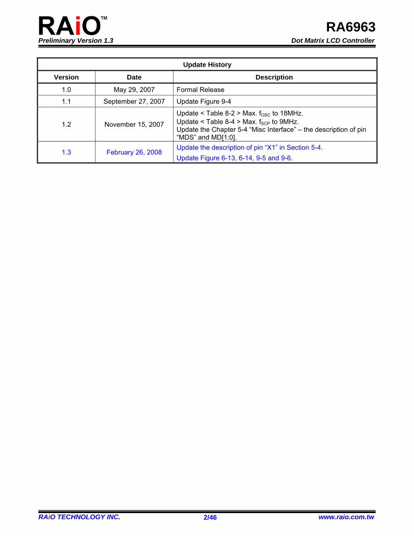
Update History
Version Date Description
1.0 May 29, 2007 Formal Release
1.1 September 27, 2007 Update Figure 9-4
1.2 November 15, 2007 Update < Table 8-2 > Max. fOSC to 18MHz. Update < Table 8-4 > Max. fSCP to 9MHz. Update the Chapter 5-4 “Misc Interface” – the description of pin “MDS” and MD[1:0].
1.3 February 26, 2008 Update the description of pin “X1” in Section 5-4. Update Figure 6-13, 6-14, 9-5 and 9-6.
Preliminary Version 1.3 Dot Matrix LCD Controller
RAiO TECHNOLOGY INC. www.raio.com.tw 3/46
RA6963
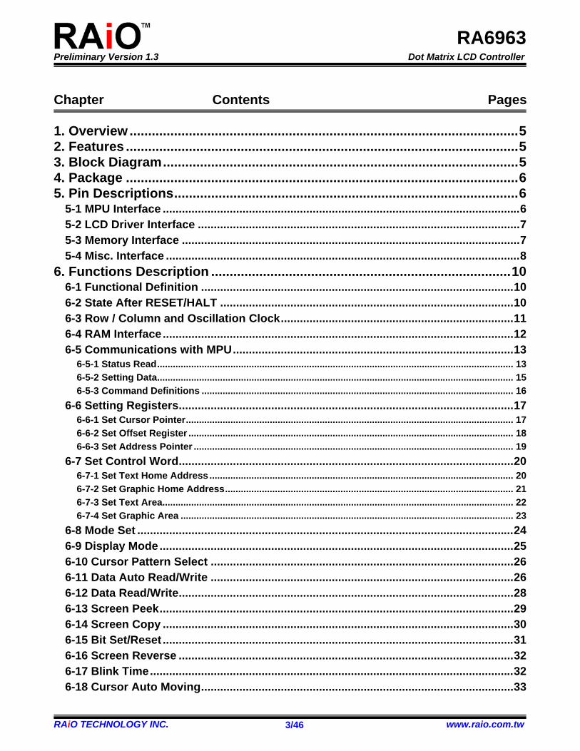
Chapter Contents Pages 1. Overview .........................................................................................................5 2. Features ..........................................................................................................5 3. Block Diagram................................................................................................5 4. Package ..........................................................................................................6 5. Pin Descriptions.............................................................................................6
5-1 MPU Interface ................................................................................................................6 5-2 LCD Driver Interface .....................................................................................................7 5-3 Memory Interface ..........................................................................................................7 5-4 Misc. Interface ...............................................................................................................8
6. Functions Description .................................................................................10 6-1 Functional Definition ..................................................................................................10 6-2 State After RESET/HALT ............................................................................................10 6-3 Row / Column and Oscillation Clock.........................................................................11 6-4 RAM Interface..............................................................................................................12 6-5 Communications with MPU........................................................................................13
6-5-1 Status Read........................................................................................................................................ 13 6-5-2 Setting Data........................................................................................................................................ 15 6-5-3 Command Definitions ....................................................................................................................... 16
6-6 Setting Registers.........................................................................................................17 6-6-1 Set Cursor Pointer............................................................................................................................. 17 6-6-2 Set Offset Register ............................................................................................................................ 18 6-6-3 Set Address Pointer .......................................................................................................................... 19
6-7 Set Control Word.........................................................................................................20 6-7-1 Set Text Home Address .................................................................................................................... 20 6-7-2 Set Graphic Home Address.............................................................................................................. 21 6-7-3 Set Text Area...................................................................................................................................... 22 6-7-4 Set Graphic Area ............................................................................................................................... 23
6-8 Mode Set ......................................................................................................................24 6-9 Display Mode...............................................................................................................25 6-10 Cursor Pattern Select ...............................................................................................26 6-11 Data Auto Read/Write ...............................................................................................26 6-12 Data Read/Write.........................................................................................................28 6-13 Screen Peek...............................................................................................................29 6-14 Screen Copy ..............................................................................................................30 6-15 Bit Set/Reset ..............................................................................................................31 6-16 Screen Reverse .........................................................................................................32 6-17 Blink Time..................................................................................................................32 6-18 Cursor Auto Moving..................................................................................................33
Preliminary Version 1.3 Dot Matrix LCD Controller
RAiO TECHNOLOGY INC. www.raio.com.tw 4/46
RA6963
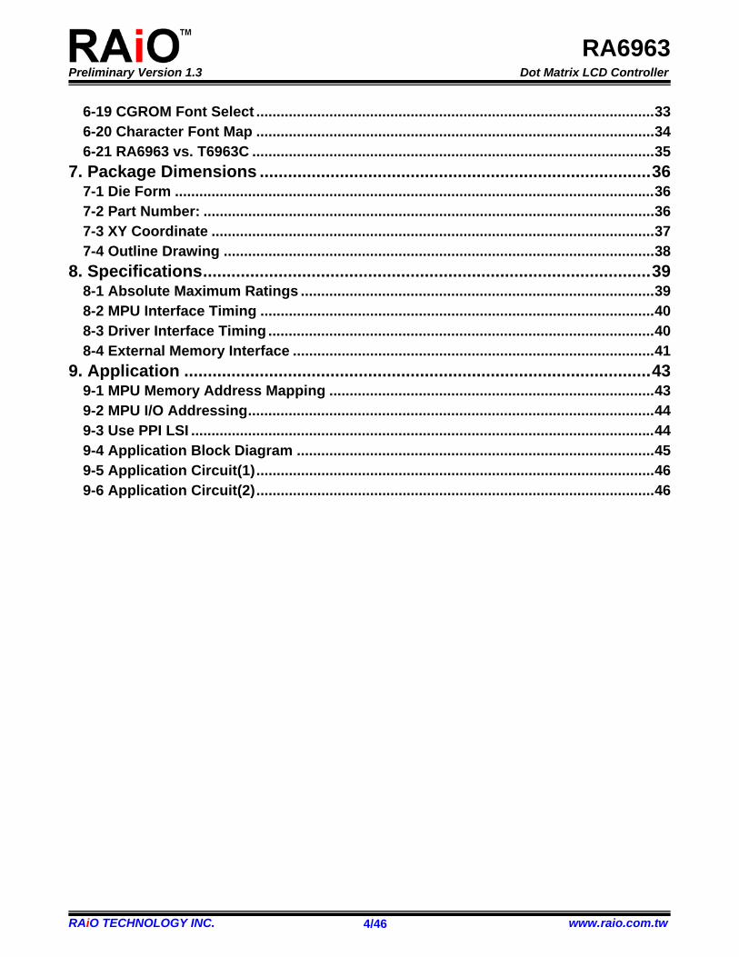
6-19 CGROM Font Select ..................................................................................................33 6-20 Character Font Map ..................................................................................................34 6-21 RA6963 vs. T6963C ...................................................................................................35
7. Package Dimensions ...................................................................................36 7-1 Die Form ......................................................................................................................36 7-2 Part Number: ...............................................................................................................36 7-3 XY Coordinate .............................................................................................................37 7-4 Outline Drawing ..........................................................................................................38
8. Specifications...............................................................................................39 8-1 Absolute Maximum Ratings .......................................................................................39 8-2 MPU Interface Timing .................................................................................................40 8-3 Driver Interface Timing ...............................................................................................40 8-4 External Memory Interface .........................................................................................41
9. Application ...................................................................................................43 9-1 MPU Memory Address Mapping ................................................................................43 9-2 MPU I/O Addressing....................................................................................................44 9-3 Use PPI LSI ..................................................................................................................44 9-4 Application Block Diagram ........................................................................................45 9-5 Application Circuit(1)..................................................................................................46 9-6 Application Circuit(2)..................................................................................................46
Preliminary Version 1.3 Dot Matrix LCD Controller
RAiO TECHNOLOGY INC. www.raio.com.tw 5/46
RA6963
1. Overview
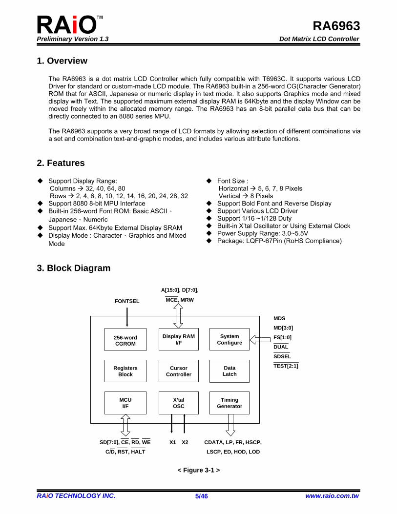
The RA6963 is a dot matrix LCD Controller which fully compatible with T6963C. It supports various LCD Driver for standard or custom-made LCD module. The RA6963 built-in a 256-word CG(Character Generator) ROM that for ASCII, Japanese or numeric display in text mode. It also supports Graphics mode and mixed display with Text. The supported maximum external display RAM is 64Kbyte and the display Window can be moved freely within the allocated memory range. The RA6963 has an 8-bit parallel data bus that can be directly connected to an 8080 series MPU. The RA6963 supports a very broad range of LCD formats by allowing selection of different combinations via a set and combination text-and-graphic modes, and includes various attribute functions.
2. Features
Support Display Range: Columns 32, 40, 64, 80 Rows 2, 4, 6, 8, 10, 12, 14, 16, 20, 24, 28, 32
Support 8080 8-bit MPU Interface Built-in 256-word Font ROM: Basic ASCII、
Japanese、Numeric Support Max. 64Kbyte External Display SRAM Display Mode : Character、Graphics and Mixed
Mode
Font Size : Horizontal 5, 6, 7, 8 Pixels Vertical 8 Pixels
Support Bold Font and Reverse Display Support Various LCD Driver Support 1/16 ~1/128 Duty Built-in X’tal Oscillator or Using External Clock Power Supply Range: 3.0~5.5V Package: LQFP-67Pin (RoHS Compliance)
3. Block Diagram
Display RAM I/F
256-wordCGROM
SD[7:0], CE, RD, WE X1 X2 CDATA, LP, FR, HSCP,
C/D, RST, HALT LSCP, ED, HOD, LOD
RegistersBlock
TimingGenerator
MCUI/F
Cursor Controller
X’tal OSC
DataLatch
System Configure
A[15:0], D[7:0],
MCE, MRW
MDS
MD[3:0]
FS[1:0]
DUAL
SDSEL
TEST[2:1]
FONTSEL
< Figure 3-1 >
Preliminary Version 1.3 Dot Matrix LCD Controller
RAiO TECHNOLOGY INC. www.raio.com.tw 6/46
RA6963
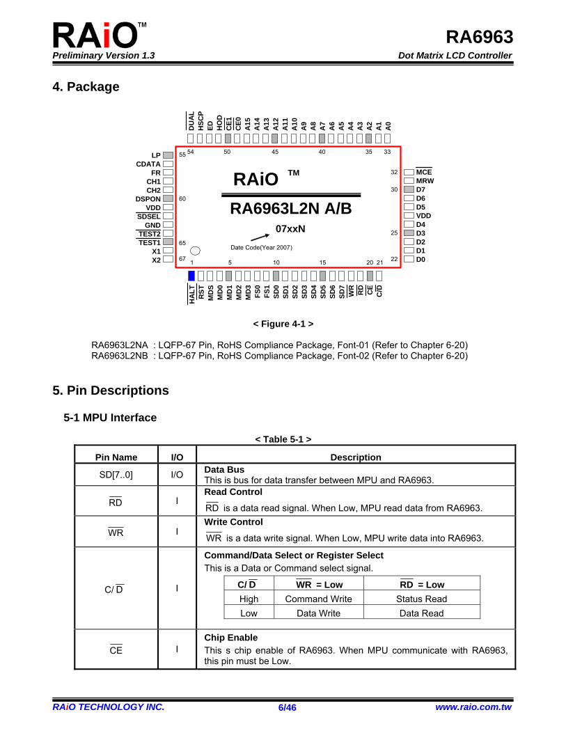
4. Package
RAiORA6963L2N A/B
TM
07xxN
LPCDATA
FRCH1CH2
DSPONVDD
SDSELGND
TEST2TEST1
X1X2
Date Code(Year 2007)
1 5 10 15 20 21
32
30
25
22
54 50 45 40 35 3355
60
65
67
MCEMRWD7D6D5VDDD4D3D2D1D0
DU
AL
HSC
PED H
OD
CE1
CE0
A15
A14
A13
A12
A11
A10
A9
A8
A7
A6
A5
A4
A3
A2
A1
A0
HA
LTR
STM
DS
MD
0M
D1
MD
2M
D3
FS0
FS1
SD0
SD1
SD2
SD3
SD4
SD5
SD6
SD7
WR
RD CE
C/D
< Figure 4-1 >
RA6963L2NA : LQFP-67 Pin, RoHS Compliance Package, Font-01 (Refer to Chapter 6-20) RA6963L2NB : LQFP-67 Pin, RoHS Compliance Package, Font-02 (Refer to Chapter 6-20)
5. Pin Descriptions
5-1 MPU Interface
< Table 5-1 >
Pin Name I/O Description
SD[7..0] I/O Data Bus This is bus for data transfer between MPU and RA6963.
RD I Read Control
RD is a data read signal. When Low, MPU read data from RA6963.
WR I Write Control
WR is a data write signal. When Low, MPU write data into RA6963.
C/ D I
Command/Data Select or Register Select This is a Data or Command select signal.
C/ D WR = Low RD = Low High Command Write Status Read Low Data Write Data Read
CE I Chip Enable This s chip enable of RA6963. When MPU communicate with RA6963, this pin must be Low.
Preliminary Version 1.3 Dot Matrix LCD Controller
RAiO TECHNOLOGY INC. www.raio.com.tw 7/46
RA6963
5-2 LCD Driver Interface
< Table 5-2 >
Pin Name I/O Description FR O Frame
LP O Latch Latch pulse for column driver. Shift clock pulse for Row Driver
CDATA O Synchronous Data Synchronous Data for Row Driver.
HSCP O Shift Clock Pulse Shift clock pulse for Column Driver in upper area of LCD.
HOD O Data Output Data output for Odd Columns in upper area of LCD.
ED O
Data Output SDSEL = High Data output for even columns in both upper and lower area of LCD. SDSEL = Low Data output for columns in both upper and lower area of LCD.
DSPON O Display On Display On/Off control signal. When HALT or RST is Low, DSPON output Low (LCD Display Off).
5-3 Memory Interface
< Table 5-3 >
Pin Name I/O Description
A[15:0] O Address Output for External Memory
D[7:0] I/O Data Bus for External Memory
MCE O
Memory Chip Enable MCE= Low Memory Enable. MCE = High Memory Disable.
MRW O Memory Read/Write Control MRW = Low Memory Write Enable. MRW = High Memory Read Enable.
0CE
LOD O
Memory Chip Enable 0 If DUAL = High Chip enable pin for display memory in the address range 0000~07FFh. If DUAL = Low Serial data output for odd columns in lower area of LCD.
1CE
LSCP O
Memory Chip Enable 1 If DUAL = High Chip enable pin for display memory in the address range 0800~0FFFh. If DUAL = Low Shift clock output for Column Driver in lower area of LCD.
VDD P Power GND P Ground
Preliminary Version 1.3 Dot Matrix LCD Controller
RAiO TECHNOLOGY INC. www.raio.com.tw 8/46
RA6963
5-4 Misc. Interface
< Table 5-4 >
Pin Name I/O Description
DUAL I Scan Select DUAL = Low Dual-Scan Mode. DUAL = High Signal-Scan Mode.
MDS MD[1:0] I
LCD Size Selection One Screen:
DUAL H H H H H H H H MDS L L L L H H H H MD1 H H L L H H L L MD0 H L H L H L H L Lines 2 4 6 8 10 12 14 16
V-Dots 16 32 48 64 80 96 112 128 Two Screens:
DUAL L L L L L L L L MDS L L L L H H H H MD1 H H L L H H L L MD0 H L H L H L H L Lines 4 8 12 16 20 24 28 32
V-Dots 32 64 96 128 160 192 224 256
X1 I
Crystal Oscillator Input A crystal oscillator circuit is built in. The oscillation frequency is adjusted according to the display size. If using an external clock, use the X1 pin as the clock input. (X2 open.) External capacitors 15 to 20pF.
X2 O Crystal Oscillator Output
FS[1:0] I
Font Selection FS0 H L H L FS1 H H L L Font 5 X 8 6 X 8 7 X 8 8 X 8
MD[3:2] I
Columns Selection MD2 H L H L MD3 H H L L
Columns 32 40 64 80
SDSEL I Data Transfer Mode SDSEL = Low Sending data by simple serial mode. SDSEL = High Sending data by odd/even separtion mode.
Preliminary Version 1.3 Dot Matrix LCD Controller
RAiO TECHNOLOGY INC. www.raio.com.tw 9/46
RA6963
HALT I Halt Signal HALT = Low Stop the Clock. HALT = High Normal Mode.
RST I Reset Signal RST = Low RA6963 will be reset. RST = High Normal mode. RA6963 built-in a Pull-Hi resistor.
]1:2[TEST I Test Pins These are test pins. No need for connection(NC).
CH1, CH2 O Check Signals
FONTSEL I
CGROM Font Select This pin is used to select the character of CGROM. Refer to Chapter 6-20. Please note, this pin is only reserved for die base chip only. Refer to Chapter 7-2. FONTSEL = Low Select default CGROM Font-01. FONTSEL = High Select default CGROM Font-02.
Preliminary Version 1.3 Dot Matrix LCD Controller
RAiO TECHNOLOGY INC. www.raio.com.tw 10/46
RA6963
6. Functions Description
6-1 Functional Definition
After power on, it is necessary to reset. The RST is kept Low between 5 clocks up (oscillation clock).
When HALT = Low, the oscillation stops. The power supply for the LCD must be turned off, to protect the LCD from DC bias.
The HALT function(HALT = Low) includes the RESET function(RST =Low). The column/line counter and display register are cleared by RST . (Other registers are not cleared.) Disable the display using the clear-display register
The status must be checked before data or commands are sent. The MSB=0 status check must be done in particular. There is a possibility of erroneous operation due to a hard interrupt.
STA0 and STA1 must be checked at the same time. When a command is executed, data transmission errors may occur.
The RA6963 can only handle one byte per machine cycle (16 clocks). It is impossible to send more than two data in a machine cycle.
When using a command with operand data, it important to send the data first, and then executes the command.
The character fonts used by the RA6963 are different from ASCII codes.
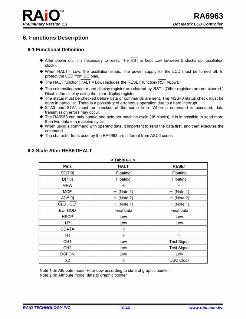
6-2 State After RESET/HALT
< Table 6-1 > Pins HALT RESET
SD[7:0] Floating Floating D[7:0] Floating Floating MRW Hi Hi MCE Hi (Note 1) Hi (Note 1)
A[15:0] Hi (Note 2) Hi (Note 2) 0CE , 1CE Hi (Note 1) Hi (Note 1)
ED, HOD Final data Final data HSCP Low Low
LP Low Low CDATA Hi Hi
FR Hi Hi CH1 Low Test Signal CH2 Low Test Signal
DSPON Low Low X2 Hi OSC Clock
Note 1 :In Attribute mode, Hi or Low according to state of graphic pointer Note 2 :In Attribute mode, data to graphic pointer
Preliminary Version 1.3 Dot Matrix LCD Controller
RAiO TECHNOLOGY INC. www.raio.com.tw 11/46
RA6963
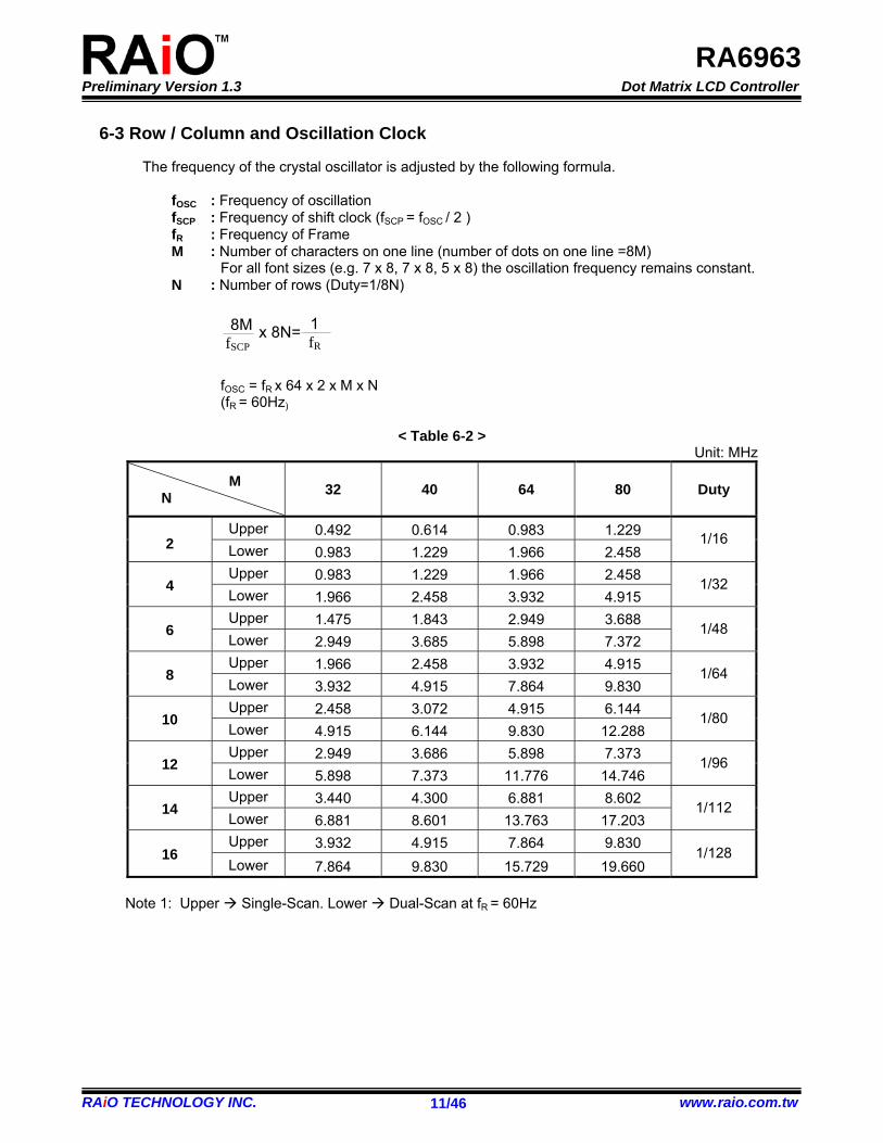
6-3 Row / Column and Oscillation Clock
The frequency of the crystal oscillator is adjusted by the following formula.
fOSC : Frequency of oscillation fSCP : Frequency of shift clock (fSCP = fOSC / 2 ) fR : Frequency of Frame M : Number of characters on one line (number of dots on one line =8M)
For all font sizes (e.g. 7 x 8, 7 x 8, 5 x 8) the oscillation frequency remains constant. N : Number of rows (Duty=1/8N)
8M fSCP
x 8N= 1fR
fOSC = fR x 64 x 2 x M x N (fR = 60Hz)
< Table 6-2 >
Unit: MHz
M N 32 40 64 80 Duty
Upper 0.492 0.614 0.983 1.229 2 Lower 0.983 1.229 1.966 2.458
1/16
Upper 0.983 1.229 1.966 2.458 4
Lower 1.966 2.458 3.932 4.915 1/32
Upper 1.475 1.843 2.949 3.688 6
Lower 2.949 3.685 5.898 7.372 1/48
Upper 1.966 2.458 3.932 4.915 8
Lower 3.932 4.915 7.864 9.830 1/64
Upper 2.458 3.072 4.915 6.144 10
Lower 4.915 6.144 9.830 12.288 1/80
Upper 2.949 3.686 5.898 7.373 12
Lower 5.898 7.373 11.776 14.746 1/96
Upper 3.440 4.300 6.881 8.602 14
Lower 6.881 8.601 13.763 17.203 1/112
Upper 3.932 4.915 7.864 9.830 16
Lower 7.864 9.830 15.729 19.660 1/128
Note 1: Upper Single-Scan. Lower Dual-Scan at fR = 60Hz
Preliminary Version 1.3 Dot Matrix LCD Controller
RAiO TECHNOLOGY INC. www.raio.com.tw 12/46
RA6963
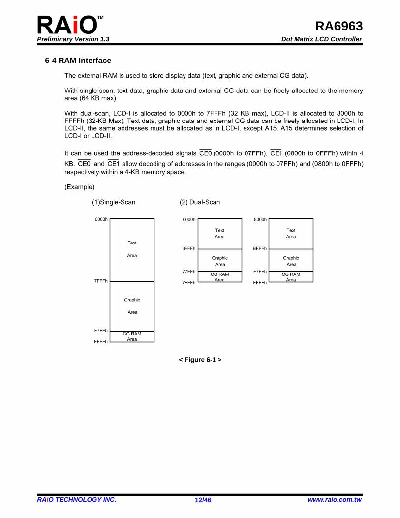
6-4 RAM Interface
The external RAM is used to store display data (text, graphic and external CG data). With single-scan, text data, graphic data and external CG data can be freely allocated to the memory area (64 KB max). With dual-scan, LCD-I is allocated to 0000h to 7FFFh (32 KB max), LCD-II is allocated to 8000h to FFFFh (32-KB Max). Text data, graphic data and external CG data can be freely allocated in LCD-I. In LCD-II, the same addresses must be allocated as in LCD-I, except A15. A15 determines selection of LCD-I or LCD-II. It can be used the address-decoded signals 0CE (0000h to 07FFh), 1CE (0800h to 0FFFh) within 4 KB. 0CE and 1CE allow decoding of addresses in the ranges (0000h to 07FFh) and (0800h to 0FFFh) respectively within a 4-KB memory space. (Example)
(1)Single-Scan (2) Dual-Scan
0000h
7FFFh
F7FFh
FFFFh
0000h
3FFFh
77FFh
7FFFh
TextArea
GraphicArea
CG RAMArea
8000h
BFFFh
F7FFh
FFFFh
TextArea
GraphicArea
CG RAMArea
Text
Area
Graphic
Area
CG RAMArea
< Figure 6-1 >
Preliminary Version 1.3 Dot Matrix LCD Controller
RAiO TECHNOLOGY INC. www.raio.com.tw 13/46
RA6963
6-5 Communications with MPU
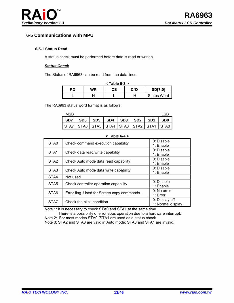
6-5-1 Status Read
A status check must be performed before data is read or written. Status Check The Status of RA6963 can be read from the data lines.
< Table 6-3 >
RD WR CS C/D SD[7:0] L H L H Status Word
The RA6963 status word format is as follows:
MSB LSB SD7 SD6 SD5 SD4 SD3 SD2 SD1 SD0 STA7 STA6 STA5 STA4 STA3 STA2 STA1 STA0
< Table 6-4 >
STA0 Check command execution capability 0: Disable 1: Enable
STA1 Check data read/write capability 0: Disable 1: Enable
STA2 Check Auto mode data read capability 0: Disable 1: Enable
STA3 Check Auto mode data write capability 0: Disable 1: Enable
STA4 Not used
STA5 Check controller operation capability 0: Disable 1: Enable
STA6 Error flag. Used for Screen copy commands. 0: No error 1: Error
STA7 Check the blink condition 0: Display off 1: Normal display
Note 1: It is necessary to check STA0 and STA1 at the same time. There is a possibility of erroneous operation due to a hardware interrupt.
Note 2: For most modes STA0 /STA1 are used as a status check. Note 3: STA2 and STA3 are valid in Auto mode; STA0 and STA1 are invalid.
Preliminary Version 1.3 Dot Matrix LCD Controller
RAiO TECHNOLOGY INC. www.raio.com.tw 14/46
RA6963
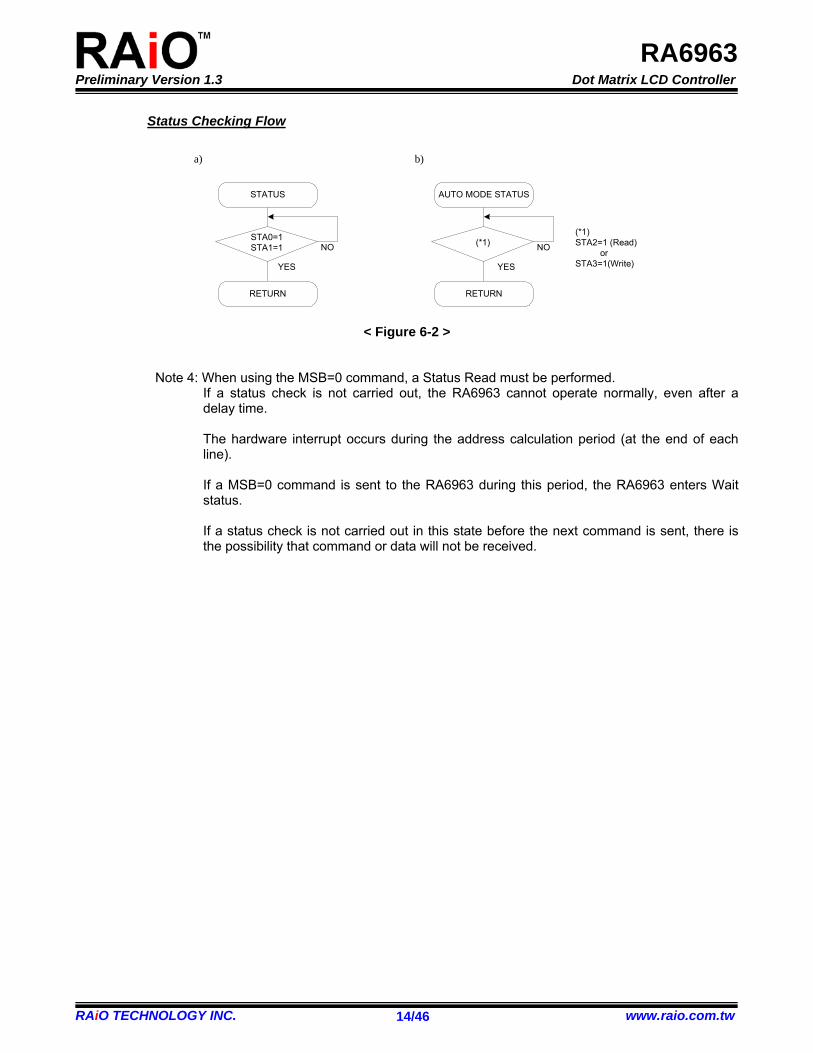
Status Checking Flow
STATUS
STA0=1STA1=1 NO
RETURN
a)
YES
AUTO MODE STATUS
(*1) NO
RETURN
YES
(*1)STA2=1 (Read) or STA3=1(Write)
b)
< Figure 6-2 > Note 4: When using the MSB=0 command, a Status Read must be performed.
If a status check is not carried out, the RA6963 cannot operate normally, even after a delay time. The hardware interrupt occurs during the address calculation period (at the end of each line). If a MSB=0 command is sent to the RA6963 during this period, the RA6963 enters Wait status. If a status check is not carried out in this state before the next command is sent, there is the possibility that command or data will not be received.
Preliminary Version 1.3 Dot Matrix LCD Controller
RAiO TECHNOLOGY INC. www.raio.com.tw 15/46
RA6963
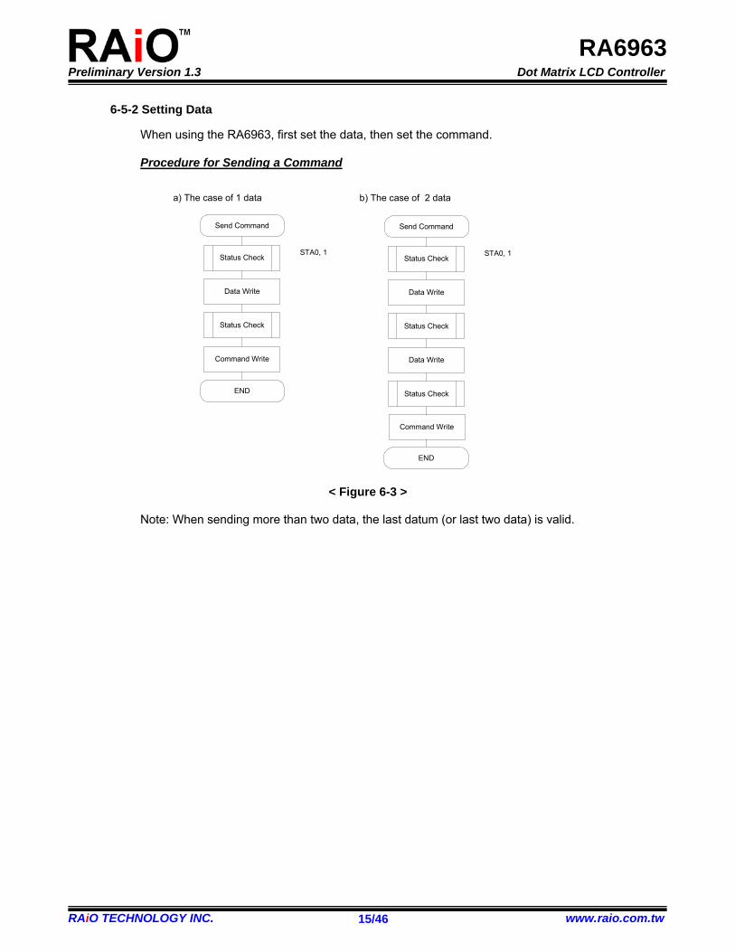
6-5-2 Setting Data
When using the RA6963, first set the data, then set the command. Procedure for Sending a Command
Send Command
Status Check
Data Write
Status Check
Command Write
END
STA0, 1
Send Command
Status Check
Data Write
Status Check
Data Write
STA0, 1
a) The case of 1 data b) The case of 2 data
Status Check
Command Write
END
< Figure 6-3 >
Note: When sending more than two data, the last datum (or last two data) is valid.
Preliminary Version 1.3 Dot Matrix LCD Controller
RAiO TECHNOLOGY INC. www.raio.com.tw 16/46
RA6963
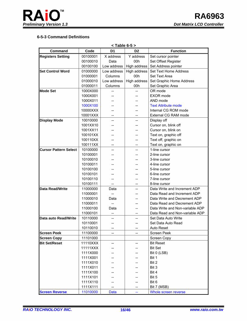
6-5-3 Command Definitions
< Table 6-5 > Command Code D1 D2 Function
Registers Setting 00100001 00100010 00100100
X address Data
Low address
Y address00h
High address
Set cursor pointer Set Offset Register Set Address pointer
Set Control Word 01000000 01000001 01000010 01000011
Low addressColumns
Low addressColumns
High address00h
High address00h
Set Text Home Address Set Text Area Set Graphic Home Address Set Graphic Area
Mode Set 1000X000 1000X001 1000X011 1000X100 10000XXX 10001XXX
-- -- -- -- -- --
-- -- -- -- -- --
OR mode EXOR mode AND mode Text Attribute mode Internal CG ROM mode External CG RAM mode
Display Mode 10010000 1001XX10 1001XX11 100101XX 100110XX 100111XX
-- -- -- -- -- --
-- -- -- -- -- --
Display off Cursor on, blink off Cursor on, blink on Text on, graphic off Text off, graphic on Text on, graphic on
Cursor Pattern Select 10100000 10100001 10100010 10100011 10100100 10100101 10100110 10100111
-- -- -- -- -- -- -- --
-- -- -- -- -- -- -- --
1-line cursor 2-line cursor 3-line cursor 4-line cursor 5-line cursor 6-line cursor 7-line cursor 8-line cursor
Data Read/Write 11000000 11000001 11000010 11000011 11000100 11000101
Data --
Data --
Data --
-- -- -- -- -- --
Data Write and Increment ADP Data Read and Increment ADP Data Write and Decrement ADP Data Read and Decrement ADP Data Write and Non-variable ADPData Read and Non-variable ADP
Data auto Read/Write 10110000 10110001 10110010
-- -- --
-- -- --
Set Data Auto Write Set Data Auto Read Auto Reset
Screen Peek 11100000 -- -- Screen Peek Screen Copy 11101000 Screen Copy Bit Set/Reset 11110XXX
11111XXX 1111X000 1111X001 1111X010 1111X011 1111X100 1111X101 1111X110 1111X111
-- -- -- -- -- -- -- -- -- --
-- -- -- -- -- -- -- -- -- --
Bit Reset Bit Set Bit 0 (LSB) Bit 1 Bit 2 Bit 3 Bit 4 Bit 5 Bit 6 Bit 7 (MSB)
Screen Reverse 11010000 Data -- Whole screen reverse
Preliminary Version 1.3 Dot Matrix LCD Controller
RAiO TECHNOLOGY INC. www.raio.com.tw 17/46
RA6963
Data Bit 0 0 : Normal 1 : Reverse
Blink Time 01010000 Data Don’t care(Note)
If Frame = 60Hz Data Bit 2:0 000 : 0.066s 001 : 0.25s 010 : 0.5s (Default) 011 : 0.75s 100 : 1s 101 : 1.25s 110 : 1.5s 111 : 2s
Cursor Auto Moving 01100000 Data Don’t care(Note)
Data Bit 0 0 : Disable.(Default) 1 : Enable.
CGROM Font Select 01110000 Data Don’t care(Note)
Data Bit 1:0 00 : Do not care.(Default) 01 : Do not care. 10 : CGROM Font-01. 11 : CGROM Font-02.
Note: In these functions, it must be sent two data before sending the command, but the contents of the second datum (D2) can be any values.
6-6 Setting Registers
< Table 6-6 > Code Hex. Function D1 D2
00100001 21h Set Cursor Pointer X-Adrs Y-Adrs 00100010 22h Set Offset Register Data 00h 00100100 24h Set Address Pointer Low Adrs High Adrs
6-6-1 Set Cursor Pointer
The X-Adrs and Y-Adrs specify the position of the cursor. The cursor position can only be moved by this command. Data read /write from the MPU never changes the cursor pointer. X-Adrs and Y-Adrs are specified as follows.
X-Adrs 00h to 4Fh (lower 7 bits are valid) Y-Adrs 00h to 1Fh (lower 5 bits are valid)
a) Single-Scan X-Adrs 00h to 4Fh
b) Dual-Scan X-Adrs 00h to 4Fh
Y-Adrs 00h to 0Fh Y-Adrs 00h to 0Fh Upper Screen
Y-Adrs 10h to 1Fh Lower Screen
Preliminary Version 1.3 Dot Matrix LCD Controller
RAiO TECHNOLOGY INC. www.raio.com.tw 18/46
RA6963
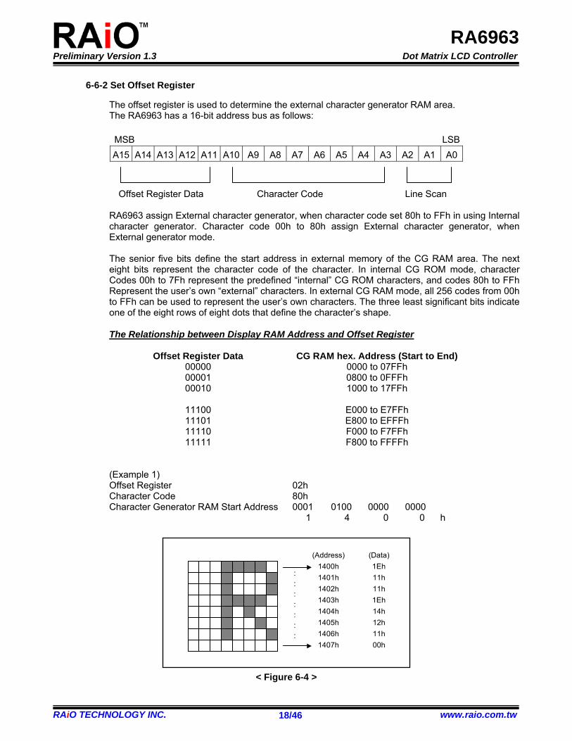
6-6-2 Set Offset Register
The offset register is used to determine the external character generator RAM area. The RA6963 has a 16-bit address bus as follows:
MSB LSB A15 A14 A13 A12 A11 A10 A9 A8 A7 A6 A5 A4 A3 A2 A1 A0
Offset Register Data Character Code Line Scan RA6963 assign External character generator, when character code set 80h to FFh in using Internal character generator. Character code 00h to 80h assign External character generator, when External generator mode. The senior five bits define the start address in external memory of the CG RAM area. The next eight bits represent the character code of the character. In internal CG ROM mode, character Codes 00h to 7Fh represent the predefined “internal” CG ROM characters, and codes 80h to FFh Represent the user’s own “external” characters. In external CG RAM mode, all 256 codes from 00h to FFh can be used to represent the user’s own characters. The three least significant bits indicate one of the eight rows of eight dots that define the character’s shape. The Relationship between Display RAM Address and Offset Register
Offset Register Data
00000 00001 00010
11100 11101 11110 11111
CG RAM hex. Address (Start to End) 0000 to 07FFh 0800 to 0FFFh 1000 to 17FFh
E000 to E7FFh E800 to EFFFh F000 to F7FFh F800 to FFFFh
(Example 1) Offset Register 02h Character Code 80h Character Generator RAM Start Address 0001 0100 0000 0000
1 4 0 0 h
(Address)1400h1401h1402h1403h1404h1405h1406h1407h
(Data)1Eh11h11h1Eh14h12h11h00h
:::::::
< Figure 6-4 >
Preliminary Version 1.3 Dot Matrix LCD Controller
RAiO TECHNOLOGY INC. www.raio.com.tw 19/46
RA6963
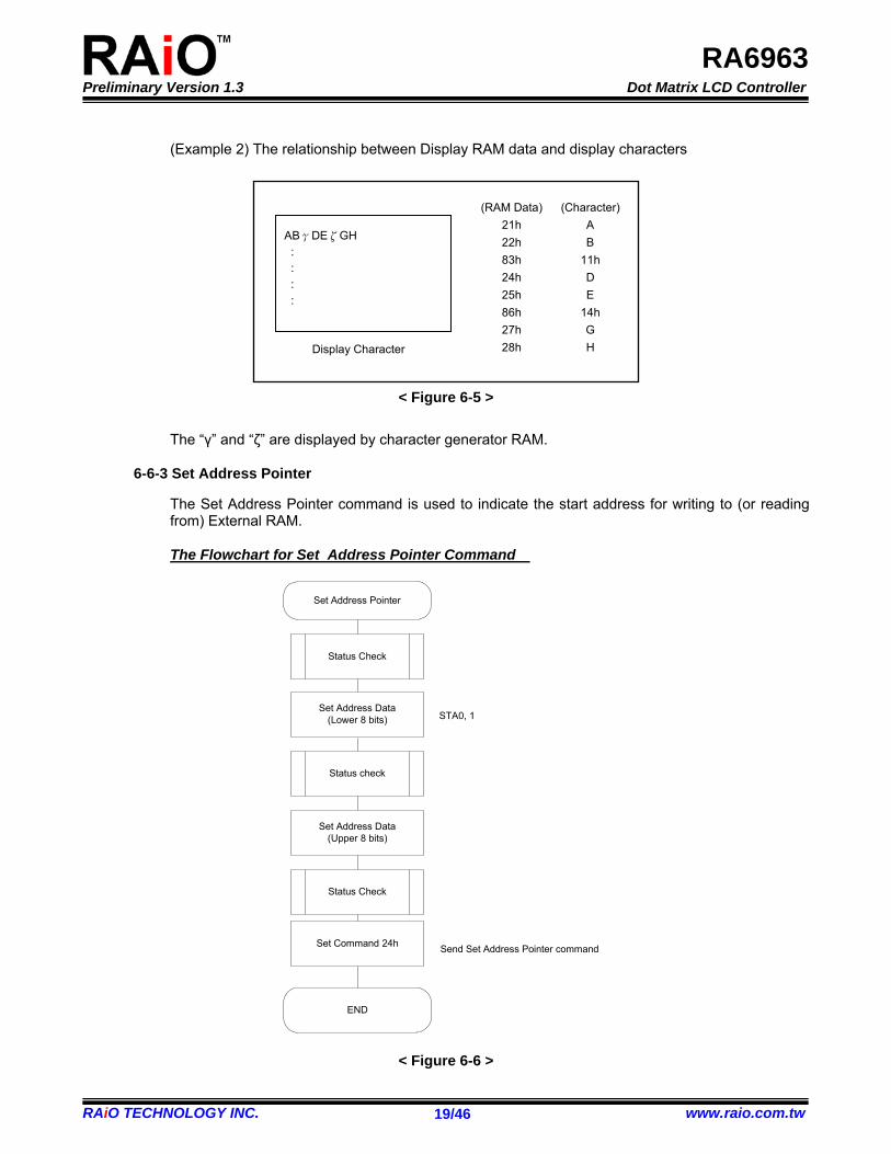
(Example 2) The relationship between Display RAM data and display characters
(RAM Data)21h22h83h24h25h86h27h28h
(Character)AB
11hDE
14hGHDisplay Character
ABγDEζGH::::
< Figure 6-5 >
The “γ” and “ζ” are displayed by character generator RAM.
6-6-3 Set Address Pointer
The Set Address Pointer command is used to indicate the start address for writing to (or reading from) External RAM. The Flowchart for Set Address Pointer Command
Set Address Pointer
Status Check
END
STA0, 1Set Address Data
(Lower 8 bits)
Status check
Set Address Data(Upper 8 bits)
Status Check
Set Command 24h Send Set Address Pointer command
< Figure 6-6 >
Preliminary Version 1.3 Dot Matrix LCD Controller
RAiO TECHNOLOGY INC. www.raio.com.tw 20/46
RA6963
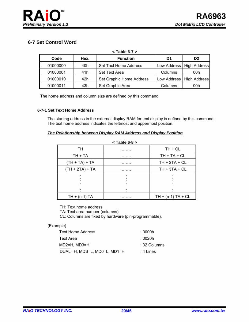
6-7 Set Control Word
< Table 6-7 > Code Hex. Function D1 D2
01000000 40h Set Text Home Address Low Address High Address01000001 41h Set Text Area Columns 00h 01000010 42h Set Graphic Home Address Low Address High Address01000011 43h Set Graphic Area Columns 00h
The home address and column size are defined by this command.
6-7-1 Set Text Home Address
The starting address in the external display RAM for text display is defined by this command. The text home address indicates the leftmost and uppermost position. The Relationship between Display RAM Address and Display Position
< Table 6-8 >
TH ……… TH + CL TH + TA ……… TH + TA + CL
(TH + TA) + TA ……… TH + 2TA + CL (TH + 2TA) + TA ……… TH + 3TA + CL
: : : :
: : : :
: : : :
TH + (n-1) TA ……… TH + (n-1) TA + CL TH: Text home address TA: Text area number (columns) CL: Columns are fixed by hardware (pin-programmable).
(Example) Text Home Address Text Area MD2=H, MD3=H DUAL =H, MDS=L, MD0=L, MD1=H
: 0000h : 0020h : 32 Columns : 4 Lines
Preliminary Version 1.3 Dot Matrix LCD Controller
RAiO TECHNOLOGY INC. www.raio.com.tw 21/46
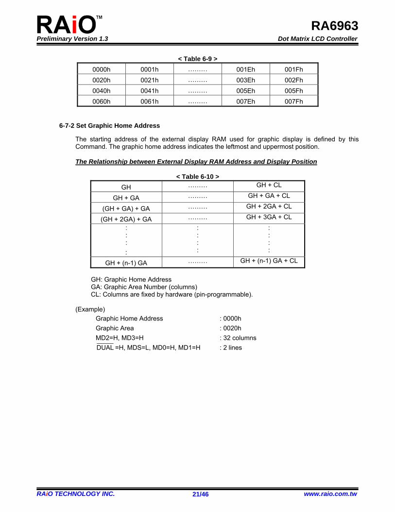
RA6963
< Table 6-9 > 0000h 0001h ……… 001Eh 001Fh 0020h 0021h ……… 003Eh 002Fh 0040h 0041h ……… 005Eh 005Fh 0060h 0061h ……… 007Eh 007Fh
6-7-2 Set Graphic Home Address
The starting address of the external display RAM used for graphic display is defined by this Command. The graphic home address indicates the leftmost and uppermost position. The Relationship between External Display RAM Address and Display Position
< Table 6-10 >
GH ……… GH + CL
GH + GA ……… GH + GA + CL
(GH + GA) + GA ……… GH + 2GA + CL
(GH + 2GA) + GA ……… GH + 3GA + CL : : : :
: : : :
: : : :
GH + (n-1) GA ……… GH + (n-1) GA + CL
GH: Graphic Home Address GA: Graphic Area Number (columns) CL: Columns are fixed by hardware (pin-programmable).
(Example)
Graphic Home Address : 0000h Graphic Area : 0020h MD2=H, MD3=H : 32 columns DUAL =H, MDS=L, MD0=H, MD1=H : 2 lines
Preliminary Version 1.3 Dot Matrix LCD Controller
RAiO TECHNOLOGY INC. www.raio.com.tw 22/46
RA6963
< Table 6-11 > 0000h 0001h ……… 001Eh 001Fh 0020h 0021h ……… 003Eh 003Fh 0040h 0041h ……… 005Eh 005Fh 0060h 0061h ……… 007Eh 007Fh 0080h 0081h ……… 009Eh 009Fh 00A0h 00A1h ……… 00BEh 00BFh 00C0h 00C1h ……… 00DEh 00DFh 00E0h 00E1h ……… 00FEh 00FFh 0100h 0101h ……… 011Eh 011Fh 0120h 0121h ……… 013Eh 013Fh 0140h 0141h ……… 015Eh 015Fh 0160h 0161h ……… 017Eh 017Fh 0180h 0181h ……… 019Eh 019Fh 01A0h 01A1h ……… 01BEh 01BFh 01C0h 01C1h ……… 01DEh 01DFh 01E0h 01E1h ……… 01FEh 01FFh
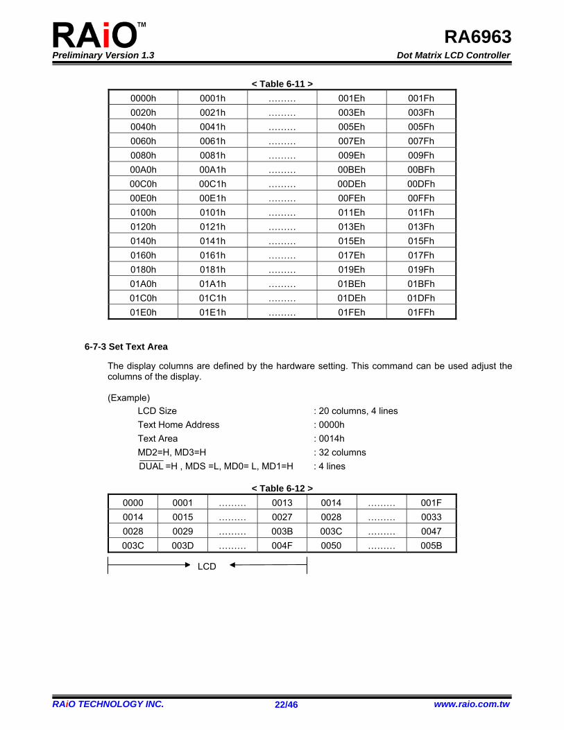
6-7-3 Set Text Area
The display columns are defined by the hardware setting. This command can be used adjust the columns of the display. (Example)
LCD Size : 20 columns, 4 lines Text Home Address : 0000h Text Area : 0014h MD2=H, MD3=H : 32 columns DUAL =H , MDS =L, MD0= L, MD1=H : 4 lines
< Table 6-12 >
0000 0001 ……… 0013 0014 ……… 001F 0014 0015 ……… 0027 0028 ……… 0033 0028 0029 ……… 003B 003C ……… 0047 003C 003D ……… 004F 0050 ……… 005B
LCD
Preliminary Version 1.3 Dot Matrix LCD Controller
RAiO TECHNOLOGY INC. www.raio.com.tw 23/46
RA6963
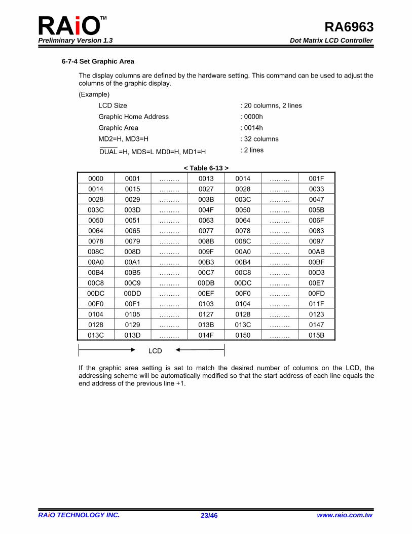
6-7-4 Set Graphic Area
The display columns are defined by the hardware setting. This command can be used to adjust the columns of the graphic display. (Example)
LCD Size : 20 columns, 2 lines Graphic Home Address : 0000h Graphic Area : 0014h MD2=H, MD3=H : 32 columns
DUAL =H, MDS=L MD0=H, MD1=H : 2 lines
< Table 6-13 > 0000 0001 ……… 0013 0014 ……… 001F 0014 0015 ……… 0027 0028 ……… 0033 0028 0029 ……… 003B 003C ……… 0047 003C 003D ……… 004F 0050 ……… 005B 0050 0051 ……… 0063 0064 ……… 006F 0064 0065 ……… 0077 0078 ……… 0083 0078 0079 ……… 008B 008C ……… 0097 008C 008D ……… 009F 00A0 ……… 00AB 00A0 00A1 ……… 00B3 00B4 ……… 00BF 00B4 00B5 ……… 00C7 00C8 ……… 00D3 00C8 00C9 ……… 00DB 00DC ……… 00E7 00DC 00DD ……… 00EF 00F0 ……… 00FD 00F0 00F1 ……… 0103 0104 ……… 011F 0104 0105 ……… 0127 0128 ……… 0123 0128 0129 ……… 013B 013C ……… 0147 013C 013D ……… 014F 0150 ……… 015B
If the graphic area setting is set to match the desired number of columns on the LCD, the addressing scheme will be automatically modified so that the start address of each line equals the end address of the previous line +1.
LCD
Preliminary Version 1.3 Dot Matrix LCD Controller
RAiO TECHNOLOGY INC. www.raio.com.tw 24/46
RA6963
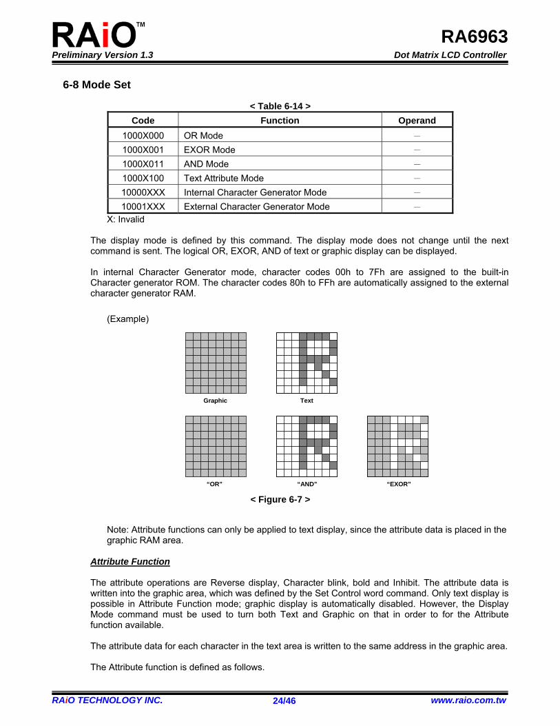
6-8 Mode Set
< Table 6-14 > Code Function Operand
1000X000 OR Mode - 1000X001 EXOR Mode - 1000X011 AND Mode - 1000X100 Text Attribute Mode - 10000XXX Internal Character Generator Mode - 10001XXX External Character Generator Mode -
X: Invalid The display mode is defined by this command. The display mode does not change until the next command is sent. The logical OR, EXOR, AND of text or graphic display can be displayed. In internal Character Generator mode, character codes 00h to 7Fh are assigned to the built-in Character generator ROM. The character codes 80h to FFh are automatically assigned to the external character generator RAM.
(Example)
Graphic Text
“OR” “AND” “EXOR”
< Figure 6-7 > Note: Attribute functions can only be applied to text display, since the attribute data is placed in the graphic RAM area.
Attribute Function The attribute operations are Reverse display, Character blink, bold and Inhibit. The attribute data is written into the graphic area, which was defined by the Set Control word command. Only text display is possible in Attribute Function mode; graphic display is automatically disabled. However, the Display Mode command must be used to turn both Text and Graphic on that in order to for the Attribute function available. The attribute data for each character in the text area is written to the same address in the graphic area. The Attribute function is defined as follows.
Preliminary Version 1.3 Dot Matrix LCD Controller
RAiO TECHNOLOGY INC. www.raio.com.tw 25/46
RA6963
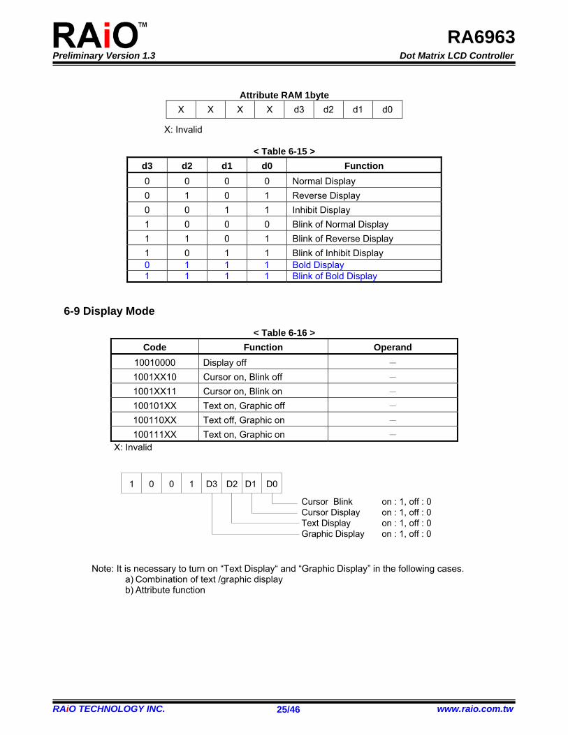
Attribute RAM 1byte
X X X X d3 d2 d1 d0
X: Invalid
< Table 6-15 > d3 d2 d1 d0 Function 0 0 0 0 Normal Display 0 1 0 1 Reverse Display 0 0 1 1 Inhibit Display 1 0 0 0 Blink of Normal Display 1 1 0 1 Blink of Reverse Display 1 0 1 1 Blink of Inhibit Display 0 1 1 1 Bold Display 1 1 1 1 Blink of Bold Display
6-9 Display Mode
< Table 6-16 > Code Function Operand
10010000 Display off - 1001XX10 Cursor on, Blink off - 1001XX11 Cursor on, Blink on - 100101XX Text on, Graphic off - 100110XX Text off, Graphic on - 100111XX Text on, Graphic on -
X: Invalid
1 0 1 D3 D2 D10 D0
Cursor Blink on : 1, off : 0Cursor Display on : 1, off : 0Text Display on : 1, off : 0 Graphic Display on : 1, off : 0
Note: It is necessary to turn on “Text Display“ and “Graphic Display” in the following cases.
a) Combination of text /graphic display b) Attribute function
Preliminary Version 1.3 Dot Matrix LCD Controller
RAiO TECHNOLOGY INC. www.raio.com.tw 26/46
RA6963
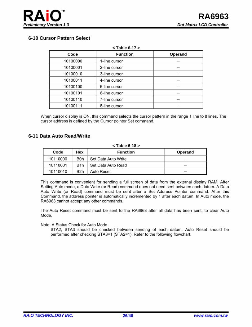
6-10 Cursor Pattern Select
< Table 6-17 > Code Function Operand
10100000 1-line cursor - 10100001 2-line cursor - 10100010 3-line cursor - 10100011 4-line cursor - 10100100 5-line cursor - 10100101 6-line cursor - 10100110 7-line cursor - 10100111 8-line cursor -
When cursor display is ON, this command selects the cursor pattern in the range 1 line to 8 lines. The cursor address is defined by the Cursor pointer Set command.
6-11 Data Auto Read/Write
< Table 6-18 > Code Hex. Function Operand
10110000 B0h Set Data Auto Write - 10110001 B1h Set Data Auto Read - 10110010 B2h Auto Reset -
This command is convenient for sending a full screen of data from the external display RAM. After Setting Auto mode, a Data Write (or Read) command does not need sent between each datum. A Data Auto Write (or Read) command must be sent after a Set Address Pointer command. After this Command, the address pointer is automatically incremented by 1 after each datum. In Auto mode, the RA6963 cannot accept any other commands. The Auto Reset command must be sent to the RA6963 after all data has been sent, to clear Auto Mode. Note: A Status Check for Auto Mode
STA2, STA3 should be checked between sending of each datum. Auto Reset should be performed after checking STA3=1 (STA2=1). Refer to the following flowchart.
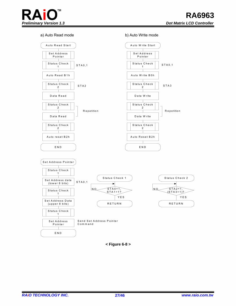
Preliminary Version 1.3 Dot Matrix LCD Controller
RAiO TECHNOLOGY INC. www.raio.com.tw 27/46
RA6963
a) Auto Read mode b) Auto Write mode
A u to R e a d S ta r t
S e t A d d re s s P o in te r
A u to R e a d B 1 h
D a ta R e a d
S ta tu s C h e c k 2
E N D
S ta tu s C h e c k 1
S ta tu s C h e c k 2
D a ta R e a d
R e p e t it io n
S ta tu s C h e c k 2
A u to re s e t B 2 h
A u to W r ite S ta r t
S e t A d d re s s P o in te r
A u to W r ite B 0 h
D a ta W r ite
S ta tu s C h e c k 2
E N D
S ta tu s C h e c k 1
S ta tu s C h e c k 2
D a ta W r ite
R e p e t it io n
S ta tu s C h e c k 2
A u to R e s e t B 2 h
S T A 0 ,1 S T A 0 ,1
S T A 3S T A 2
S e t A d d re s s P o in te r
S ta tu s C h e c k 1
E N D
S T A 0 ,1S e t A d d re s s d a ta
( lo w e r 8 b its )
S ta tu s C h e c k 1
S e t A d d re s s D a ta(u p p e r 8 b its )
S ta tu s C h e c k 1
S e t A d d re s s P o in te r
S e n d S e t A d d re s s P o in te r C o m m a n d
S ta tu s C h e c k 1
S T A 0 = 1 ,S T A 1 = 1 ?
N O
R E T U R N
Y E S
S ta tu s C h e c k 2
S T A 2 = 1 ,(S T A 3 = 1 )?
N O
R E T U R N
Y E S
< Figure 6-8 >
Preliminary Version 1.3 Dot Matrix LCD Controller
RAiO TECHNOLOGY INC. www.raio.com.tw 28/46
RA6963
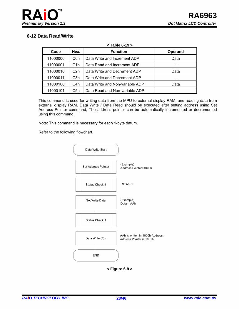
6-12 Data Read/Write
< Table 6-19 > Code Hex. Function Operand
11000000 C0h Data Write and Increment ADP Data 11000001 C1h Data Read and Increment ADP - 11000010 C2h Data Write and Decrement ADP Data 11000011 C3h Data Write and Decrement ADP - 11000100 C4h Data Write and Non-variable ADP Data 11000101 C5h Data Read and Non-variable ADP -
This command is used for writing data from the MPU to external display RAM, and reading data from external display RAM. Data Write / Data Read should be executed after setting address using Set Address Pointer command, The address pointer can be automatically incremented or decremented using this command. Note: This command is necessary for each 1-byte datum.
Refer to the following flowchart.
Data Write Start
Set Address Pointer
Status Check 1
Set Write Data
(Example)Address Pointer=1000h
Status Check 1
Data Write C0h
END
STA0, 1
(Example)Data = AAh
AAh is written in 1000h Address.Address Pointer is 1001h
< Figure 6-9 >
Preliminary Version 1.3 Dot Matrix LCD Controller
RAiO TECHNOLOGY INC. www.raio.com.tw 29/46
RA6963
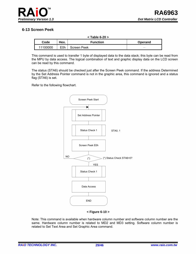
6-13 Screen Peek
< Table 6-20 > Code Hex. Function Operand
11100000 E0h Screen Peek -
This command is used to transfer 1 byte of displayed data to the data stack; this byte can be read from the MPU by data access. The logical combination of text and graphic display data on the LCD screen can be read by this command. The status (STA6) should be checked just after the Screen Peek command. If the address Determined by the Set Address Pointer command is not in the graphic area, this command is ignored and a status flag (STA6) is set.
Refer to the following flowchart.
Screen Peek Start
Set Address Pointer
Status Check 1 STA0, 1
Screen Peek E0h
(*)NO
YES
(*) Status Check STA6=0?
Status Check 1
Data Access
END
< Figure 6-10 >
Note: This command is available when hardware column number and software column number are the same. Hardware column number is related to MD2 and MD3 setting. Software column number is related to Set Text Area and Set Graphic Area command.
Preliminary Version 1.3 Dot Matrix LCD Controller
RAiO TECHNOLOGY INC. www.raio.com.tw 30/46
RA6963
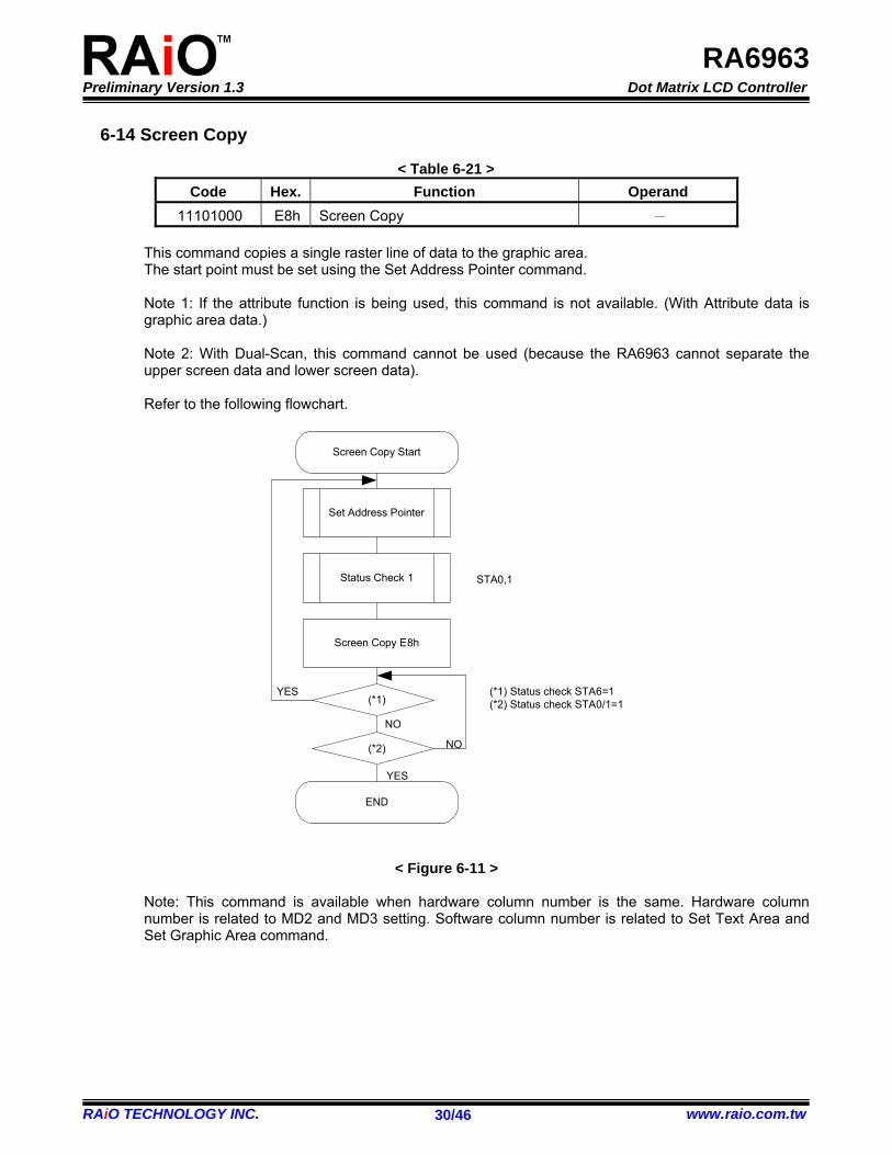
6-14 Screen Copy
< Table 6-21 > Code Hex. Function Operand
11101000 E8h Screen Copy -
This command copies a single raster line of data to the graphic area. The start point must be set using the Set Address Pointer command. Note 1: If the attribute function is being used, this command is not available. (With Attribute data is graphic area data.) Note 2: With Dual-Scan, this command cannot be used (because the RA6963 cannot separate the upper screen data and lower screen data). Refer to the following flowchart.
Screen Copy Start
Set Address Pointer
Status Check 1 STA0,1
Screen Copy E8h
(*1)
YES
(*1) Status check STA6=1(*2) Status check STA0/1=1
END
YES
NO(*2)
NO
< Figure 6-11 >
Note: This command is available when hardware column number is the same. Hardware column number is related to MD2 and MD3 setting. Software column number is related to Set Text Area and Set Graphic Area command.
Preliminary Version 1.3 Dot Matrix LCD Controller
RAiO TECHNOLOGY INC. www.raio.com.tw 31/46
RA6963
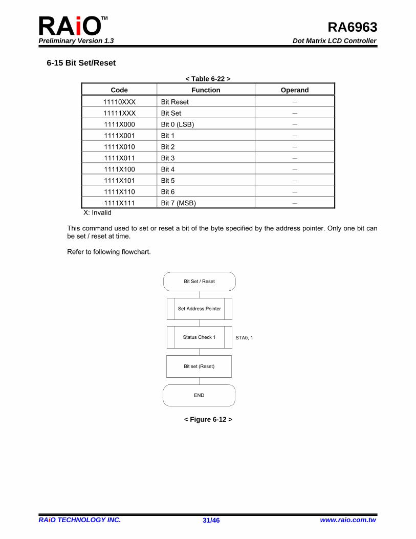
6-15 Bit Set/Reset
< Table 6-22 > Code Function Operand
11110XXX Bit Reset - 11111XXX Bit Set - 1111X000 Bit 0 (LSB) - 1111X001 Bit 1 - 1111X010 Bit 2 - 1111X011 Bit 3 - 1111X100 Bit 4 - 1111X101 Bit 5 - 1111X110 Bit 6 - 1111X111 Bit 7 (MSB) -
X: Invalid
This command used to set or reset a bit of the byte specified by the address pointer. Only one bit can be set / reset at time. Refer to following flowchart.
Bit Set / Reset
Set Address Pointer
END
STA0, 1
Bit set (Reset)
Status Check 1
< Figure 6-12 >
Preliminary Version 1.3 Dot Matrix LCD Controller
RAiO TECHNOLOGY INC. www.raio.com.tw 32/46
RA6963
6-16 Screen Reverse
<Table 6-23> Code Hex. Function D1 D2
11010000 D0h Enable/Disable the whole screen reversing Data -
<Table 6-24>
Screen Reverse Selection (D1) Bit7 Bit6 Bit5 Bit4 Bit3 Bit2 Bit1 Bit0
x x x x x x x 0/1
Bit0 = 0: Normally display. Bit0 = 1: Reverse the whole screen.
This command (D0h) is used to reverse the displayed data of the whole screen. When this function is enabled, the displayed data on the LCD are reversed to show reversing pattern.
6-17 Blink Time
<Table 6-25> Code Hex. Function D1 D2
01010000 50h Adjust the blink time for the blink functions of the
RA6963
Data (Bit2~Bit0)
Do not care (Note)
Note: In this function, it must be sent two data before sending the command, but the contents of the second datum (D2) can be any values.
<Table 6-26>
Blink Time Selection (D1) Bit 2 Bit 1 Bit 0 Blink Time(If fR=60Hz)
0 0 0 0.066 sec. 0 0 1 0.25 sec. 0 1 0 0.5 sec. 0 1 1 0.75 sec. 1 0 0 1 sec. 1 0 1 1.25 sec. 1 1 0 1.5 sec. 1 1 1 2 sec.
The blink time of the blink functions are adjusted by this command (50h). For example, if the frequency of the frame equals 60Hz, the blink time can be adjusted from 0.066 second to 2 second by using software selections. The selections are listed in the Table 6-26.
Preliminary Version 1.3 Dot Matrix LCD Controller
RAiO TECHNOLOGY INC. www.raio.com.tw 33/46
RA6963
6-18 Cursor Auto Moving
<Table 6-27> Code Hex. Function D1 D2
01100000 60h Enable/Disable the automatic cursor
movement
Data (Bit0)
Do not care (Note)
Note: In this function, it must be sent two data before sending the command, but the contents of the second datum (D2) can be any values.
<Table 6-28>
Cursor Auto Moving Selection (D1) Bit7 Bit6 Bit5 Bit4 Bit3 Bit2 Bit1 Bit0
x x x x x x x 0/1
Bit0 = 0: Disable. Bit0 = 1: Enable. The RA6963 provides a unique function for the automatic cursor movement. After writing (reading) each displayed datum, the cursor pointer is automatically increased/decreased by one in the Cursor Auto-Moving mode.
6-19 CGROM Font Select
<Table 6-29> Code Hex. Function D1 D2
01110000 70h Change the Character Font Map
Data (Bit1~Bit0)
Do not care (Note)
Note: In this function, it must be sent two data before sending the command, but the contents of the second datum (D2) can be any values.
<Table 6-30>
CGROM Font Selection (D1) Bit 1 Bit 0 CGROM Font
0 0 Do not care(Default) 0 1 Do not care 1 0 CGROM Font-01. 1 1 CGROM Font-02.
This command (70h) is a convenient function for selecting the Character Font Map. The user can get more built-in characters from CGROM Font-01 or CGROM Font-02, which is determined by software selections. The selections are listed in the Table 6-30.
Preliminary Version 1.3 Dot Matrix LCD Controller
RAiO TECHNOLOGY INC. www.raio.com.tw 34/46
RA6963
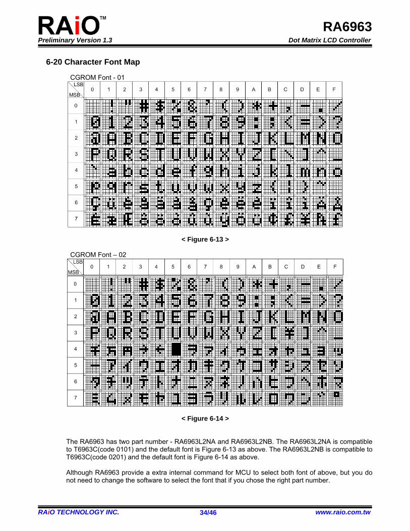
6-20 Character Font Map
CGROM Font - 01
< Figure 6-13 > CGROM Font – 02
< Figure 6-14 >
The RA6963 has two part number - RA6963L2NA and RA6963L2NB. The RA6963L2NA is compatible to T6963C(code 0101) and the default font is Figure 6-13 as above. The RA6963L2NB is compatible to T6963C(code 0201) and the default font is Figure 6-14 as above. Although RA6963 provide a extra internal command for MCU to select both font of above, but you do not need to change the software to select the font that if you chose the right part number.
Preliminary Version 1.3 Dot Matrix LCD Controller
RAiO TECHNOLOGY INC. www.raio.com.tw 35/46
RA6963
6-21 RA6963 vs. T6963C
< Table 6-23 >
Item Description RAiO RA6963
Toshiba T6963C
Note
1 CGROM Font Select Yes -- RA6963 provides two CGROMs – Font-01 and Font-02
2 Blink Time Selection Yes -- RA6963 provides eight selections for blinking.
3 Cursor Auto Move Yes -- 4 Whole Screen Reverse Yes -- 5 Bold Text and Blink Yes -- RA6963 provides Bold Text feature.
Preliminary Version 1.3 Dot Matrix LCD Controller
RAiO TECHNOLOGY INC. www.raio.com.tw 36/46
RA6963
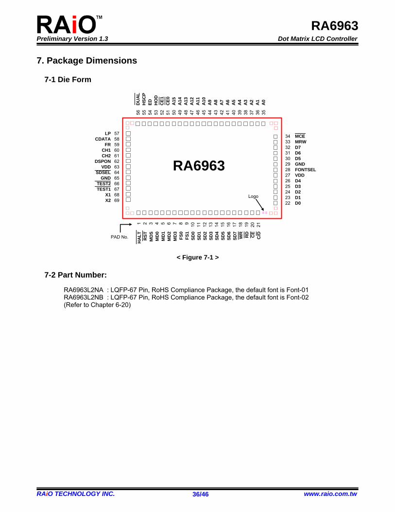
7. Package Dimensions
7-1 Die Form
RA6963
57585960616263646566676869
LPCDATA
FRCH1CH2
DSPONVDD
SDSELGND
TEST2TEST1
X1X2
HAL
TR
STM
DS
MD
0M
D1
MD
2M
D3
FS0
FS1
SD0
SD1
SD2
SD3
SD4
SD5
SD6
SD7
WR
RD CE
C/D
1 2 3 4 5 6 7 8 9 10 11 12 13 14 15 16 17 18 19 20 21
34333231302928272625242322
MCEMRWD7D6D5GNDFONTSELVDDD4D3D2D1D0
DU
ALH
SCP
ED HO
DC
E1C
E0A
15A
14A
13A
12A
11A
10A
9A
8A
7A
6A
5A
4A
3A
2A
1A
0
56 55 54 53 52 51 50 49 48 47 46 45 44 43 42 41 40 39 38 37 36 35
PAD No.
Logo
< Figure 7-1 >
7-2 Part Number:
RA6963L2NA : LQFP-67 Pin, RoHS Compliance Package, the default font is Font-01 RA6963L2NB : LQFP-67 Pin, RoHS Compliance Package, the default font is Font-02 (Refer to Chapter 6-20)
Preliminary Version 1.3 Dot Matrix LCD Controller
RAiO TECHNOLOGY INC. www.raio.com.tw 37/46
RA6963
7-3 XY Coordinate
Pad No. Pad 名稱 X 座標 Y 座標
1 HALT -1060.5 -964.65
2 RST -959.5 -964.65
3 MDS -858.5 -964.65
4 MD0 -757.5 -964.65
5 MD1 -656.5 -964.65
6 MD2 -555.5 -964.65
7 MD3 -454.5 -964.65
8 FS0 -353.5 -964.65
9 FS1 -252.5 -964.65
10 SD0 -151.5 -964.65
11 SD1 -50.5 -964.65
12 SD2 50.5 -964.65
13 SD3 151.5 -964.65
14 SD4 252.5 -964.65
15 SD5 353.5 -964.65
16 SD6 454.5 -964.65
17 SD7 555.5 -964.65
18 WR 656.5 -964.65
19 RD 757.5 -964.65
20 CE 858.5 -964.65
21 C/ D 959.5 -964.65
22 D0 1320.4 -704.75
23 D1 1320.4 -603.75
24 D2 1320.4 -502.75
25 D3 1320.4 -401.75
26 D4 1320.4 -300.75
27 VDD 1320.4 -199.75
28 FONTSEL 1320.4 -98.75
29 GND 1320.4 10.25
30 D5 1320.4 115.25
31 D6 1320.4 216.25
32 D7 1320.4 317.25
33 MRW 1320.4 418.25
34 MCE 1320.4 519.25
Pad No. Pad 名稱 X 座標 Y 座標
35 A0 1060.5 964.65
36 A1 959.5 964.65
37 A2 858.5 964.65
38 A3 757.5 964.65
39 A4 656.5 964.65
40 A5 555.5 964.65
41 A6 454.5 964.65
42 A7 353.5 964.65
43 A8 252.5 964.65
44 A9 151.5 964.65
45 A10 50.5 964.65
46 A11 -50.5 964.65
47 A12 -151.5 964.65
48 A13 -252.5 964.65
49 A14 -353.5 964.65
50 A15 -454.5 964.65
51 0CE -555.5 964.65
52 1CE -656.5 964.65
53 HOD -757.5 964.65
54 ED -858.5 964.65
55 HSCP -959.5 964.65
56 DUAL -1060.5 964.65
57 LP -1320.4 591.45
58 CDATA -1320.4 490.45
59 FR -1320.4 389.45
60 CH1 -1320.4 288.45
61 CH2 -1320.4 187.45
62 DSPON -1320.4 86.45
63 VDD -1320.4 -14.55
64 SDSEL -1320.4 -115.55
65 GND -1320.4 -224.55
66 2TEST -1320.4 -329.55
67 1TEST -1320.4 -430.55
68 X1 -1320.4 -556.8
69 X2 -1320.4 -692.8
Preliminary Version 1.3 Dot Matrix LCD Controller
RAiO TECHNOLOGY INC. www.raio.com.tw 38/46
RA6963
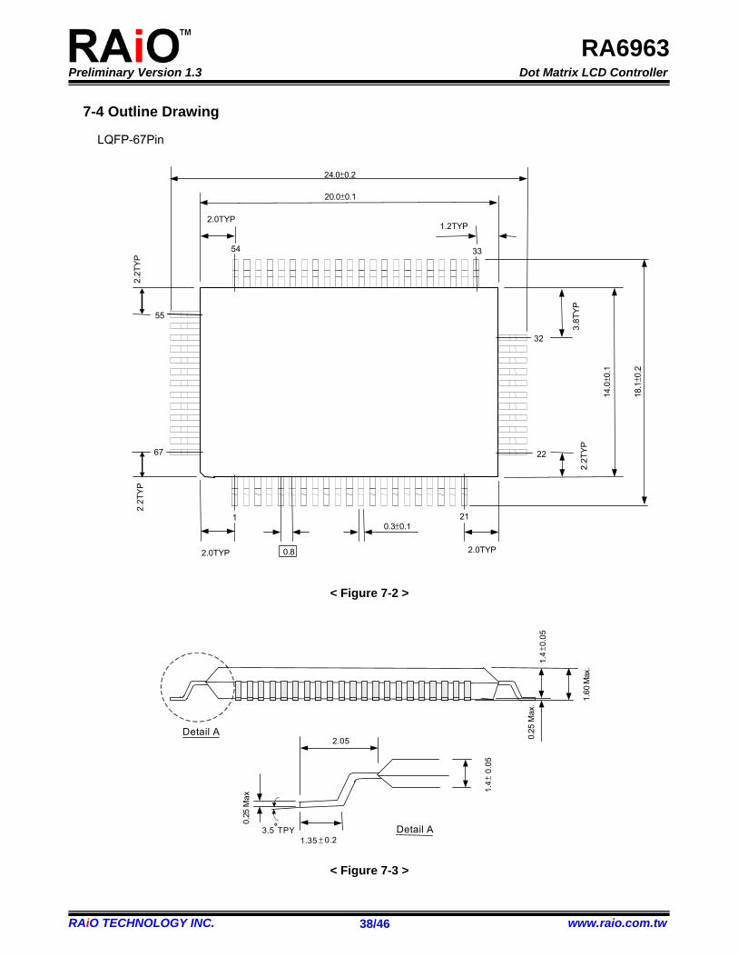
7-4 Outline Drawing
LQFP-67Pin
3.8T
YP
14.0±0
.1
2.2T
YP
20.0±0.1
33
1.2TYP
24.0±0.2
54
2.0TYP
210.3±0.1
0.8
1
18.1±0
.2
2.0TYP
2.2T
YP
2.0TYP
55
67
32
22
2.2T
YP
< Figure 7-2 >
1.60
Max
.
1.4±
0.05
0.25
Max
.
Detail A
0.25
Max
1.35 ± 0.2
1.4±
0.05
2.05
3.5°TPY Detail A
< Figure 7-3 >
Preliminary Version 1.3 Dot Matrix LCD Controller
RAiO TECHNOLOGY INC. www.raio.com.tw 39/46
RA6963
8. Specifications
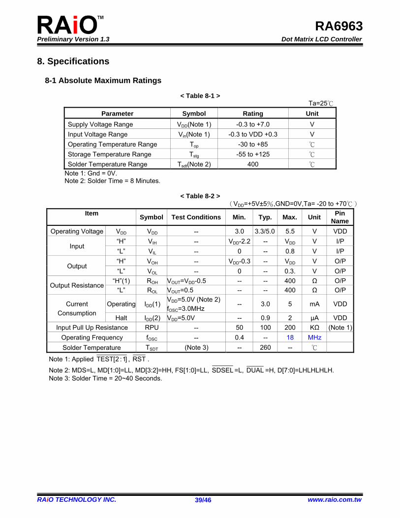
8-1 Absolute Maximum Ratings
< Table 8-1 > Ta=25
Parameter Symbol Rating Unit Supply Voltage Range VDD(Note 1) -0.3 to +7.0 V Input Voltage Range Vin(Note 1) -0.3 to VDD +0.3 V Operating Temperature Range Top -30 to +85 Storage Temperature Range Tstg -55 to +125 Solder Temperature Range Tsdt(Note 2) 400
Note 1: Gnd = 0V. Note 2: Solder Time = 8 Minutes.
< Table 8-2 > (VDD=+5V±5%,GND=0V,Ta= -20 to +70)
Item Symbol Test Conditions Min. Typ. Max. Unit Pin
NameOperating Voltage VDD VDD -- 3.0 3.3/5.0 5.5 V VDD
“H” VIH -- VDD-2.2 -- VDD V I/P Input
“L” VIL -- 0 -- 0.8 V I/P “H” VOH -- VDD-0.3 -- VDD V O/P
Output “L” VOL -- 0 -- 0.3. V O/P
“H”(1) ROH VOUT=VDD-0.5 -- -- 400 Ω O/P Output Resistance
“L” ROL VOUT=0.5 -- -- 400 Ω O/P
Operating IDD(1) VDD=5.0V (Note 2)fOSC=3.0MHz
-- 3.0 5 mA VDD Current Consumption
Halt IDD(2) VDD=5.0V -- 0.9 2 μA VDD Input Pull Up Resistance RPU -- 50 100 200 KΩ (Note 1)
Operating Frequency fOSC -- 0.4 -- 18 MHz Solder Temperature TSDT (Note 3) -- 260 --
Note 1: Applied ]1:2[TEST , RST .
Note 2: MDS=L, MD[1:0]=LL, MD[3:2]=HH, FS[1:0]=LL, SDSEL =L, DUAL =H, D[7:0]=LHLHLHLH. Note 3: Solder Time = 20~40 Seconds.
Preliminary Version 1.3 Dot Matrix LCD Controller
RAiO TECHNOLOGY INC. www.raio.com.tw 40/46
RA6963
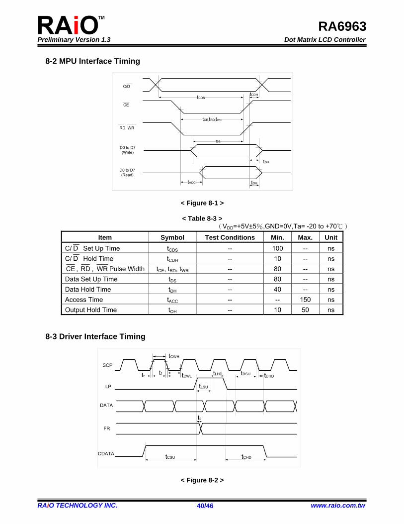
8-2 MPU Interface Timing
C/D
CE
RD, WR
D0 to D7(Write)
D0 to D7(Read)
tCDStCDH
tACC
tCE,tRD,tWR
tDS
tDH
tOH
< Figure 8-1 >
< Table 8-3 > (VDD=+5V±5%,GND=0V,Ta= -20 to +70)
Item Symbol Test Conditions Min. Max. UnitC/ D Set Up Time tCDS -- 100 -- ns C/ D Hold Time tCDH -- 10 -- ns CE , RD , WR Pulse Width tCE, tRD, tWR -- 80 -- ns Data Set Up Time tDS -- 80 -- ns Data Hold Time tDH -- 40 -- ns Access Time tACC -- -- 150 ns Output Hold Time tOH -- 10 50 ns
8-3 Driver Interface Timing
SCP
LP
DATA
FR
CDATA
tr tf
tCWH
tCWL tLHD
tLSU
tDSU tDHD
td
tCSU tCHD
< Figure 8-2 >
Preliminary Version 1.3 Dot Matrix LCD Controller
RAiO TECHNOLOGY INC. www.raio.com.tw 41/46
RA6963
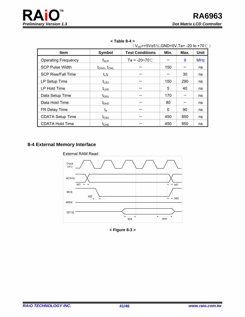
< Table 8-4 >
(VDD=+5V±5%,GND=0V,Ta= -20 to +70)
Item Symbol Test Conditions Min. Max. Unit
Operating Frequency fSCP Ta = -20~70 -- 9 MHz
SCP Pulse Width tCWH, tCWL -- 150 -- ns
SCP Rise/Fall Time tr,tf -- -- 30 ns
LP Setup Time tLSU -- 150 290 ns
LP Hold Time tLHD -- 5 40 ns
Data Setup Time tDSU -- 170 -- ns
Data Hold Time tDHD -- 80 -- ns
FR Delay Time td -- 0 90 ns
CDATA Setup Time tCSU -- 450 850 ns
CDATA Hold Time tCHD -- 450 950 ns
8-4 External Memory Interface
External RAM Read
Clock(X1)
A[15:0]
MCE
MRW
D[7:0]
td1
td2
tDS tDH
td1
td3
< Figure 8-3 >
Preliminary Version 1.3 Dot Matrix LCD Controller
RAiO TECHNOLOGY INC. www.raio.com.tw 42/46
RA6963
External RAM Write
Clock(X1)
A[15:0]
MCE
MRW
D[7:0]
td1 td1
td6
td8
td4
td5
td7
td9
< Figure 8-4 >
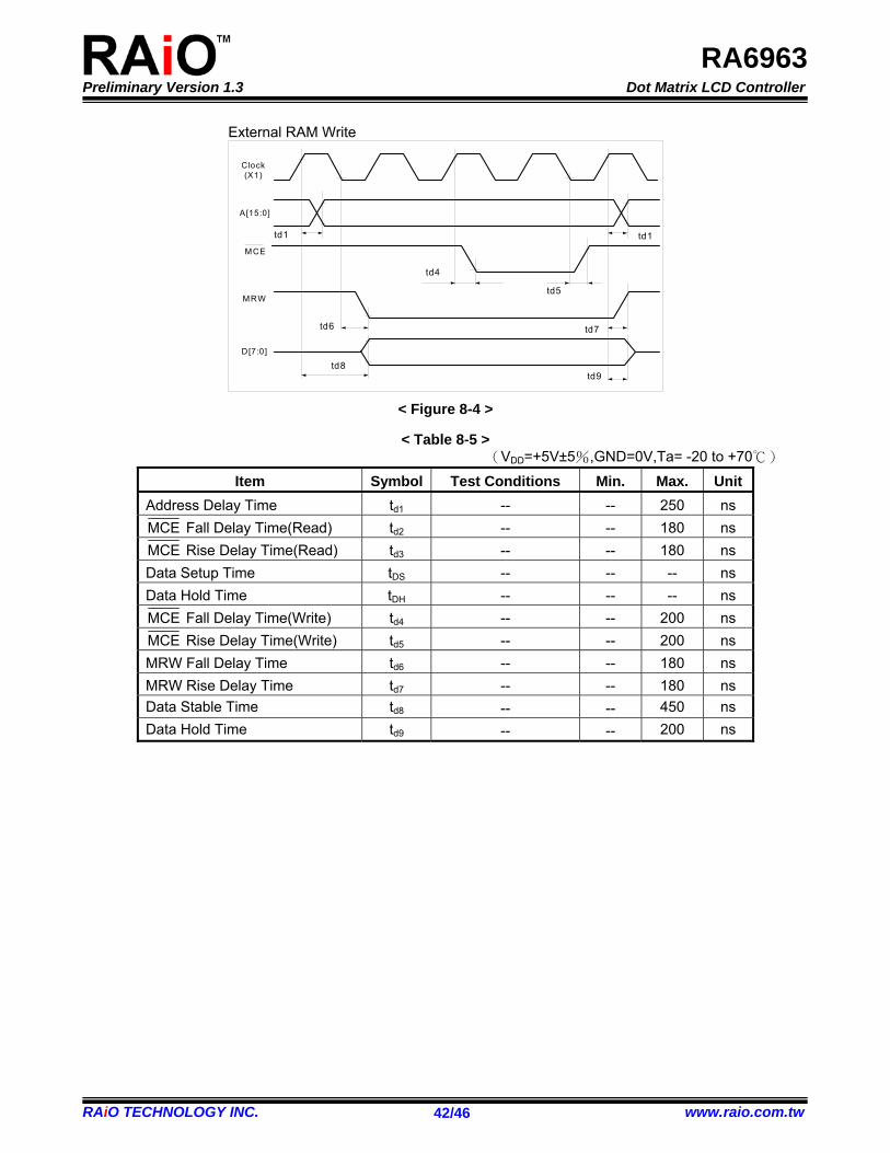
< Table 8-5 > (VDD=+5V±5%,GND=0V,Ta= -20 to +70)
Item Symbol Test Conditions Min. Max. UnitAddress Delay Time td1 -- -- 250 ns MCE Fall Delay Time(Read) td2 -- -- 180 ns MCE Rise Delay Time(Read) td3 -- -- 180 ns Data Setup Time tDS -- -- -- ns Data Hold Time tDH -- -- -- ns MCE Fall Delay Time(Write) td4 -- -- 200 ns MCE Rise Delay Time(Write) td5 -- -- 200 ns MRW Fall Delay Time td6 -- -- 180 ns MRW Rise Delay Time td7 -- -- 180 ns Data Stable Time td8 -- -- 450 ns Data Hold Time td9 -- -- 200 ns
Preliminary Version 1.3 Dot Matrix LCD Controller
RAiO TECHNOLOGY INC. www.raio.com.tw 43/46
RA6963
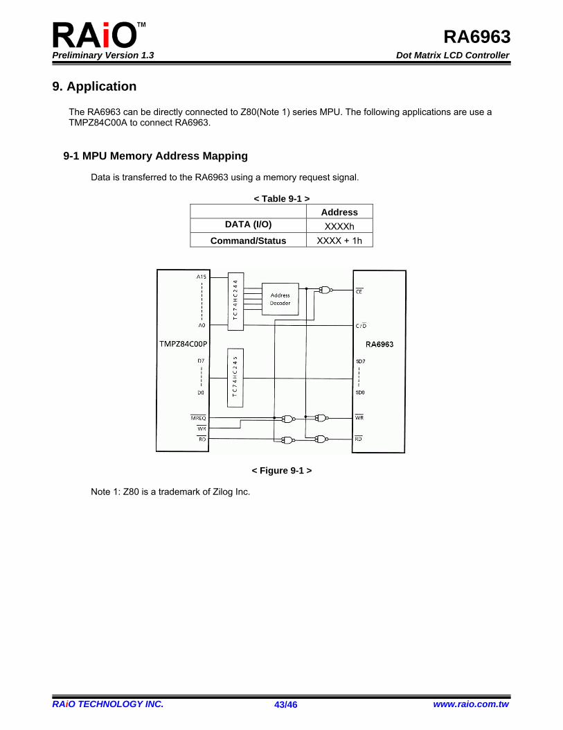
9. Application
The RA6963 can be directly connected to Z80(Note 1) series MPU. The following applications are use a TMPZ84C00A to connect RA6963.
9-1 MPU Memory Address Mapping
Data is transferred to the RA6963 using a memory request signal.
< Table 9-1 > Address
DATA (I/O) XXXXh Command/Status XXXX + 1h
< Figure 9-1 > Note 1: Z80 is a trademark of Zilog Inc.
Preliminary Version 1.3 Dot Matrix LCD Controller
RAiO TECHNOLOGY INC. www.raio.com.tw 44/46
RA6963
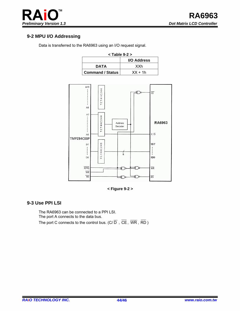
9-2 MPU I/O Addressing
Data is transferred to the RA6963 using an I/O request signal.
< Table 9-2 > I/O Address
DATA XXh Command / Status XX + 1h
< Figure 9-2 >
9-3 Use PPI LSI
The RA6963 can be connected to a PPI LSI. The port A connects to the data bus. The port C connects to the control bus. (C/ D , CE , WR , RD )
Preliminary Version 1.3 Dot Matrix LCD Controller
RAiO TECHNOLOGY INC. www.raio.com.tw 45/46
RA6963
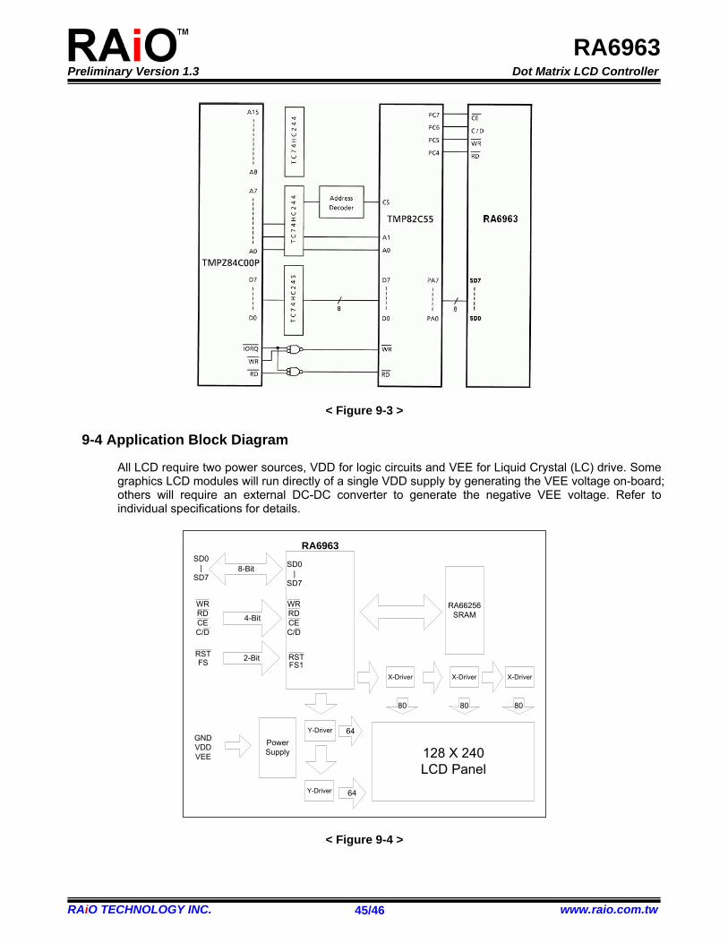
< Figure 9-3 >
9-4 Application Block Diagram
All LCD require two power sources, VDD for logic circuits and VEE for Liquid Crystal (LC) drive. Some graphics LCD modules will run directly of a single VDD supply by generating the VEE voltage on-board; others will require an external DC-DC converter to generate the negative VEE voltage. Refer to individual specifications for details.
SD0|
SD78-Bit SD0
|SD7
WRRDCEC/D
RSTFS1
4-Bit
2-Bit
WRRDCEC/D
RSTFS
RA66256 SRAM
128 X 240 LCD Panel
X-Driver X-Driver X-Driver
Y-Driver
Y-Driver
64
64
80 80 80
Power Supply
GNDVDDVEE
RA6963
< Figure 9-4 >
Preliminary Version 1.3 Dot Matrix LCD Controller
RAiO TECHNOLOGY INC. www.raio.com.tw 46/46
RA6963
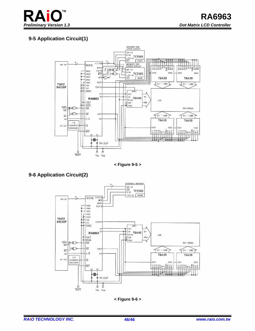
9-5 Application Circuit(1)
< Figure 9-5 >
9-6 Application Circuit(2)
< Figure 9-6 >