Embed Size (px)
Citation preview
〇Product structure: Silicon monolithic integrated circuit 〇This product has no designed protection against radioactive rays
1/24
TSZ02201-0T5T0B500040-1-2
© 2018 ROHM Co., Ltd. All rights reserved. 23.Mar.2018 Rev.001
www.rohm.com
TSZ22111 • 14 • 001
LED Drivers for LCD Backlights
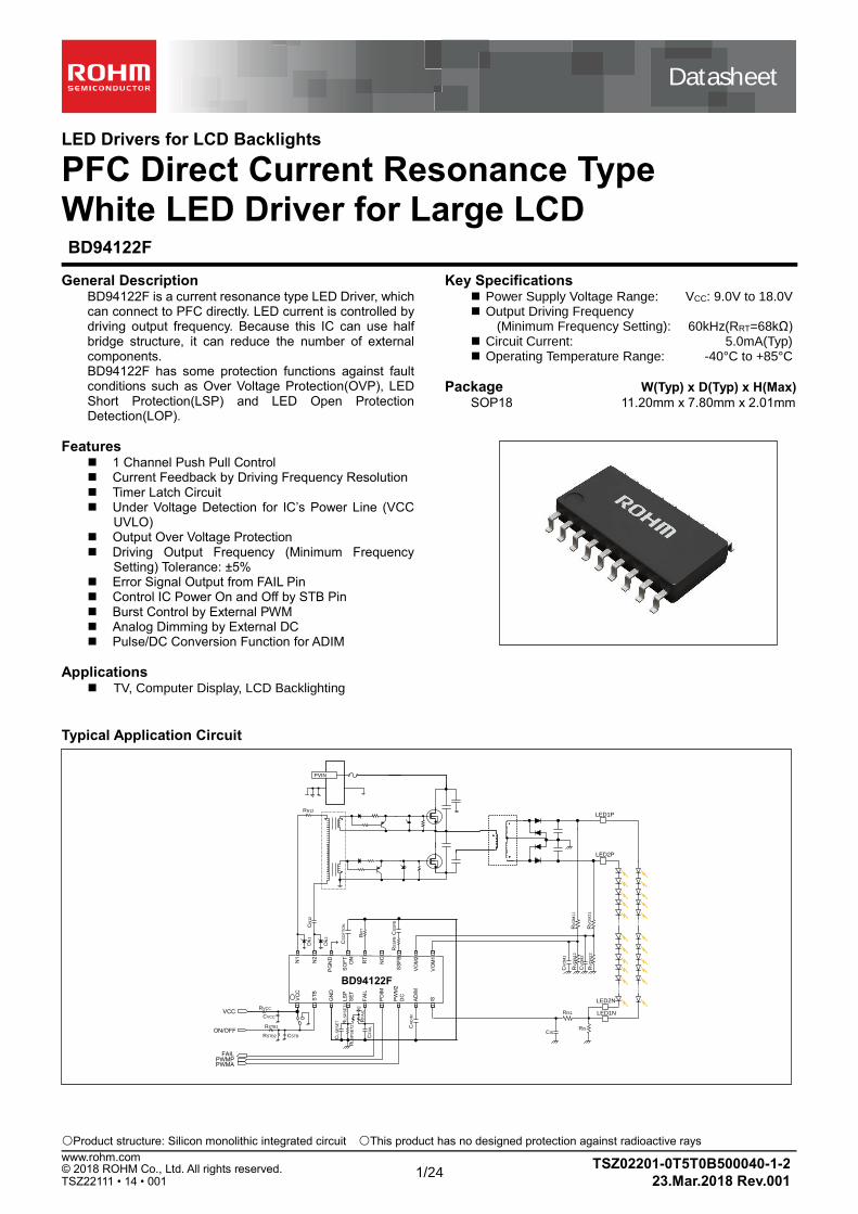
PFC Direct Current Resonance Type White LED Driver for Large LCD BD94122F
General Description BD94122F is a current resonance type LED Driver, which can connect to PFC directly. LED current is controlled by driving output frequency. Because this IC can use half bridge structure, it can reduce the number of external components. BD94122F has some protection functions against fault conditions such as Over Voltage Protection(OVP), LED Short Protection(LSP) and LED Open Protection Detection(LOP).
Features 1 Channel Push Pull Control Current Feedback by Driving Frequency Resolution Timer Latch Circuit Under Voltage Detection for IC’s Power Line (VCC
UVLO) Output Over Voltage Protection Driving Output Frequency (Minimum Frequency
Setting) Tolerance: ±5% Error Signal Output from FAIL Pin Control IC Power On and Off by STB Pin Burst Control by External PWM Analog Dimming by External DC Pulse/DC Conversion Function for ADIM
Applications TV, Computer Display, LCD Backlighting
Key Specifications Power Supply Voltage Range: VCC: 9.0V to 18.0V Output Driving Frequency
(Minimum Frequency Setting): 60kHz(RRT=68kΩ) Circuit Current: 5.0mA(Typ) Operating Temperature Range: -40°C to +85°C
Package W(Typ) x D(Typ) x H(Max) SOP18 11.20mm x 7.80mm x 2.01mm
Typical Application Circuit
PVIN
RVCC
CVCC
RSTB1
RSTB2 CSTB CL
SP
SE
T RL
SP
SE
T1
RL
SP
SE
T2
RF
AIL
CF
AIL C
AD
IM
RS
SF
BC
SS
FB
RR
T
CS
OF
TO
N
DN
2
DN
1
RV
OM
12
CV
OM
1
CV
OM
2
RV
OM
22
RV
OM
11
RV
OM
21
RIS
RIS1
CIS
LED1P
LED2P
LED2N
LED1N
CN
12
RN12
Datasheet
2/24
BD94122F
TSZ02201-0T5T0B500040-1-2
© 2018 ROHM Co., Ltd. All rights reserved. 23.Mar.2018 Rev.001
www.rohm.com
TSZ22111 • 15 • 001
Contents
General Description ........................................................................................................................................................................ 1
Features.......................................................................................................................................................................................... 1
Applications .................................................................................................................................................................................... 1
Key Specifications .......................................................................................................................................................................... 1
Package .......................................................................................................................................................................................... 1
Typical Application Circuit ............................................................................................................................................................... 1
Pin Configuration ............................................................................................................................................................................ 3
Pin Description ................................................................................................................................................................................ 3
Block Diagram ................................................................................................................................................................................ 4
Pin Function Descriptions ............................................................................................................................................................... 5
Detection Condition List of the Protection Functions ...................................................................................................................... 8
Operation List of the Protection Function ........................................................................................................................................ 8
Absolute Maximum Ratings ............................................................................................................................................................ 9
Thermal Resistance ........................................................................................................................................................................ 9
Recommended Operating Conditions ........................................................................................................................................... 10
External Components Recommended Ranges ............................................................................................................................. 10
Electrical Characteristics............................................................................................................................................................... 11
Typical Performance Curves ......................................................................................................................................................... 13
Timing Chart ................................................................................................................................................................................. 14
Application Example ..................................................................................................................................................................... 18
I/O Equivalence Circuits................................................................................................................................................................ 19
Operational Notes ......................................................................................................................................................................... 20
Ordering Information ..................................................................................................................................................................... 22
Marking Diagram .......................................................................................................................................................................... 22
Physical Dimension and Packing Information ............................................................................................................................... 23
Revision History ............................................................................................................................................................................ 24
3/24
BD94122F
TSZ02201-0T5T0B500040-1-2
© 2018 ROHM Co., Ltd. All rights reserved. 23.Mar.2018 Rev.001
www.rohm.com
TSZ22111 • 15 • 001
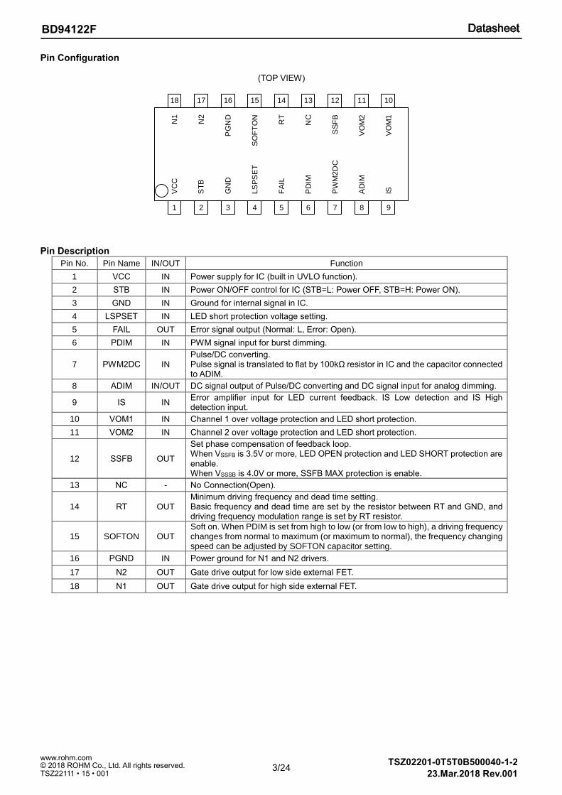
Pin Configuration
(TOP VIEW)
Pin Description
Pin No. Pin Name IN/OUT Function
1 VCC IN Power supply for IC (built in UVLO function).
2 STB IN Power ON/OFF control for IC (STB=L: Power OFF, STB=H: Power ON).
3 GND IN Ground for internal signal in IC.
4 LSPSET IN LED short protection voltage setting.
5 FAIL OUT Error signal output (Normal: L, Error: Open).
6 PDIM IN PWM signal input for burst dimming.
7 PWM2DC IN Pulse/DC converting. Pulse signal is translated to flat by 100kΩ resistor in IC and the capacitor connected to ADIM.
8 ADIM IN/OUT DC signal output of Pulse/DC converting and DC signal input for analog dimming.
9 IS IN Error amplifier input for LED current feedback. IS Low detection and IS High detection input.
10 VOM1 IN Channel 1 over voltage protection and LED short protection.
11 VOM2 IN Channel 2 over voltage protection and LED short protection.
12 SSFB OUT
Set phase compensation of feedback loop. When VSSFB is 3.5V or more, LED OPEN protection and LED SHORT protection are enable. When VSSSB is 4.0V or more, SSFB MAX protection is enable.
13 NC - No Connection(Open).
14 RT OUT Minimum driving frequency and dead time setting. Basic frequency and dead time are set by the resistor between RT and GND, and driving frequency modulation range is set by RT resistor.
15 SOFTON OUT Soft on. When PDIM is set from high to low (or from low to high), a driving frequency changes from normal to maximum (or maximum to normal), the frequency changing speed can be adjusted by SOFTON capacitor setting.
16 PGND IN Power ground for N1 and N2 drivers.
17 N2 OUT Gate drive output for low side external FET.
18 N1 OUT Gate drive output for high side external FET.
VC
CN
1
GN
D
LS
PS
ET
FA
IL
PD
IM
PW
M2
DC
AD
IM
ISST
BN
2
PG
ND
SO
FT
ON
RT
NC
SS
FB
VO
M2
VO
M1
1 2 3 4 5 6 7 8 9
101112131415161718
4/24
BD94122F
TSZ02201-0T5T0B500040-1-2
© 2018 ROHM Co., Ltd. All rights reserved. 23.Mar.2018 Rev.001
www.rohm.com
TSZ22111 • 15 • 001
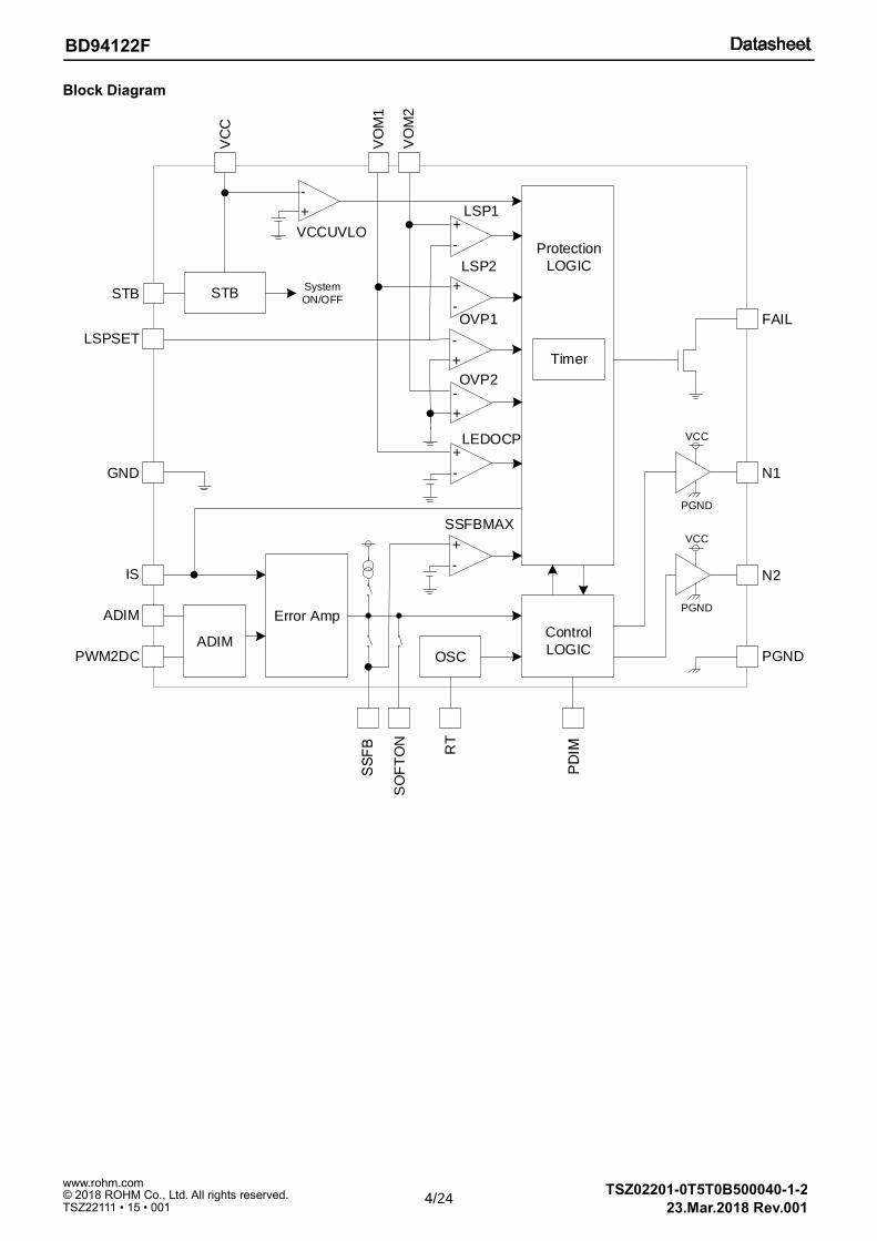
Block Diagram
Protection
LOGIC
+
-
+
-
+
-
+
-
Timer
+
-
+
-
LSP1
LSP2
OVP1
OVP2V
OM
1
VO
M2
FAIL
VC
C
STB
OSC
Control
LOGIC
N1
N2
VCCUVLO
LEDOCP
SS
FB RT
LSPSET
System
ON/OFF
PD
IM
Error Amp
ADIM
IS
ADIM
PWM2DC
VCC
PGND
VCC
PGND
PGND
STB
GND
SO
FT
ON
+
-
SSFBMAX
5/24
BD94122F
TSZ02201-0T5T0B500040-1-2
© 2018 ROHM Co., Ltd. All rights reserved. 23.Mar.2018 Rev.001
www.rohm.com
TSZ22111 • 15 • 001
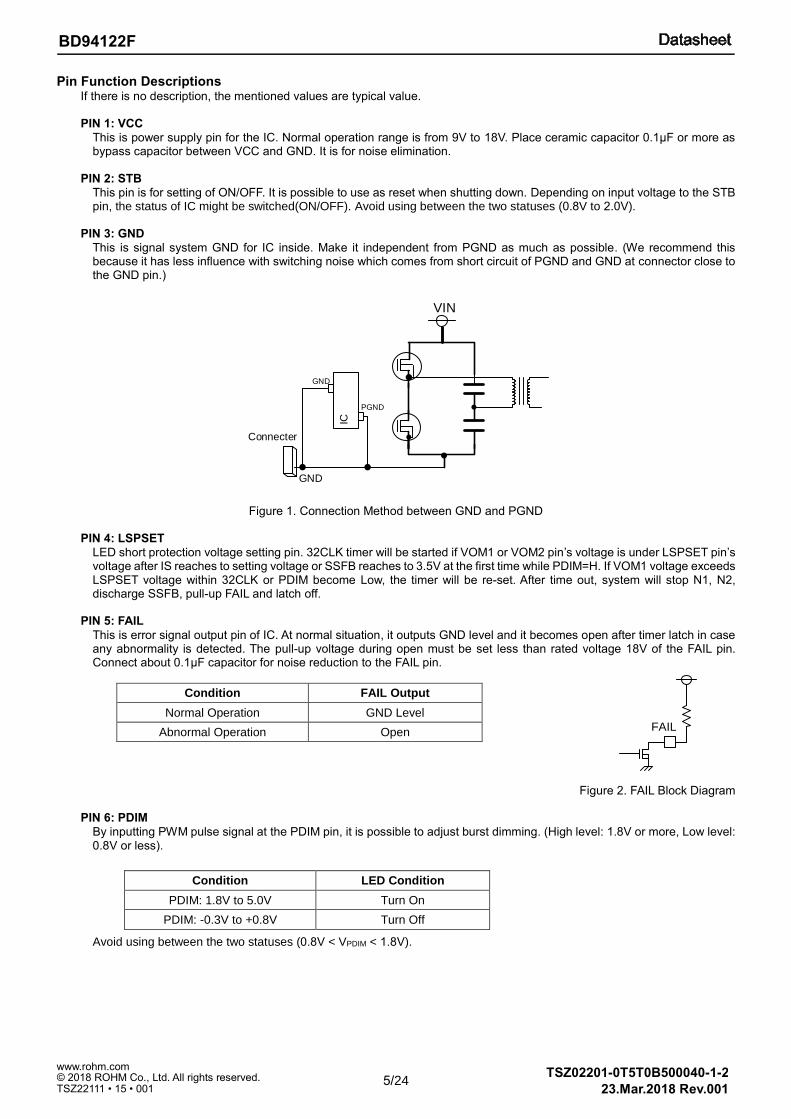
Pin Function Descriptions If there is no description, the mentioned values are typical value. PIN 1: VCC
This is power supply pin for the IC. Normal operation range is from 9V to 18V. Place ceramic capacitor 0.1µF or more as bypass capacitor between VCC and GND. It is for noise elimination.
PIN 2: STB
This pin is for setting of ON/OFF. It is possible to use as reset when shutting down. Depending on input voltage to the STB pin, the status of IC might be switched(ON/OFF). Avoid using between the two statuses (0.8V to 2.0V).
PIN 3: GND
This is signal system GND for IC inside. Make it independent from PGND as much as possible. (We recommend this because it has less influence with switching noise which comes from short circuit of PGND and GND at connector close to the GND pin.)
Figure 1. Connection Method between GND and PGND
PIN 4: LSPSET
LED short protection voltage setting pin. 32CLK timer will be started if VOM1 or VOM2 pin’s voltage is under LSPSET pin’s voltage after IS reaches to setting voltage or SSFB reaches to 3.5V at the first time while PDIM=H. If VOM1 voltage exceeds LSPSET voltage within 32CLK or PDIM become Low, the timer will be re-set. After time out, system will stop N1, N2, discharge SSFB, pull-up FAIL and latch off.
PIN 5: FAIL
This is error signal output pin of IC. At normal situation, it outputs GND level and it becomes open after timer latch in case any abnormality is detected. The pull-up voltage during open must be set less than rated voltage 18V of the FAIL pin. Connect about 0.1µF capacitor for noise reduction to the FAIL pin.
Condition FAIL Output
Normal Operation GND Level
Abnormal Operation Open
Figure 2. FAIL Block Diagram
PIN 6: PDIM
By inputting PWM pulse signal at the PDIM pin, it is possible to adjust burst dimming. (High level: 1.8V or more, Low level: 0.8V or less).
Avoid using between the two statuses (0.8V < VPDIM < 1.8V).
IC
N1
VIN
GND
GND
PGND
Connecter
Condition LED Condition
PDIM: 1.8V to 5.0V Turn On
PDIM: -0.3V to +0.8V Turn Off
FAIL
6/24
BD94122F
TSZ02201-0T5T0B500040-1-2
© 2018 ROHM Co., Ltd. All rights reserved. 23.Mar.2018 Rev.001
www.rohm.com
TSZ22111 • 15 • 001
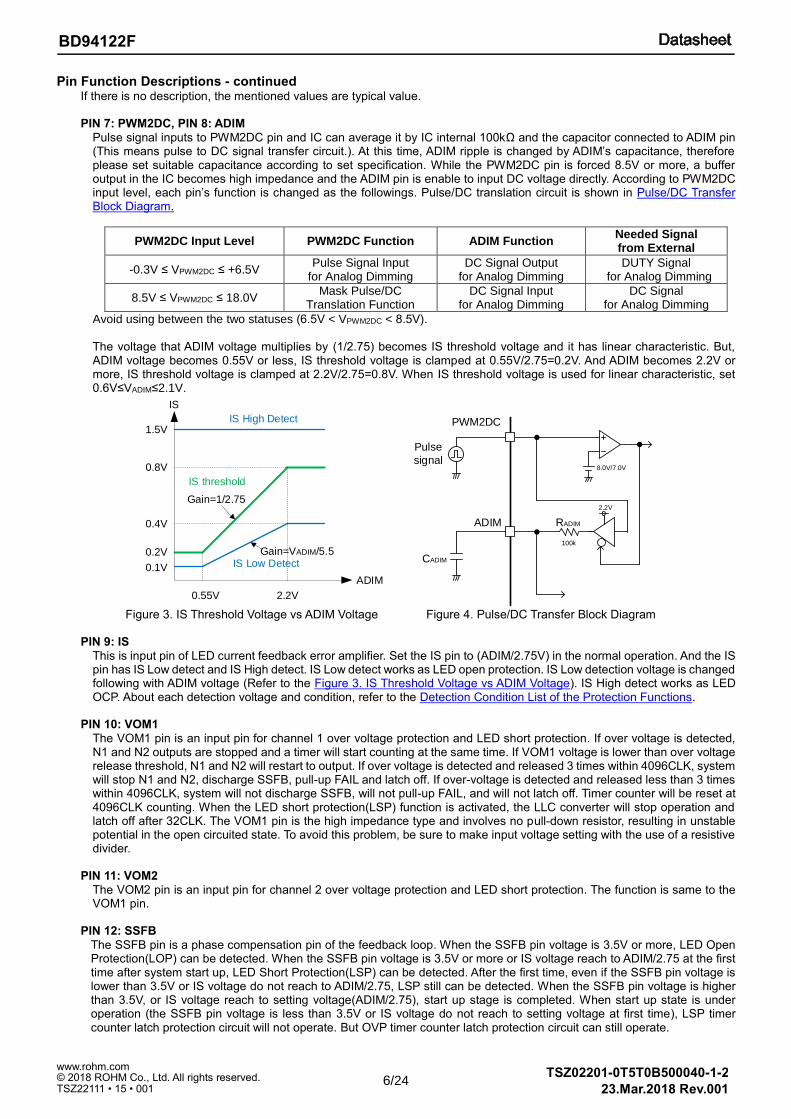
Pin Function Descriptions - continued If there is no description, the mentioned values are typical value. PIN 7: PWM2DC, PIN 8: ADIM
Pulse signal inputs to PWM2DC pin and IC can average it by IC internal 100kΩ and the capacitor connected to ADIM pin (This means pulse to DC signal transfer circuit.). At this time, ADIM ripple is changed by ADIM’s capacitance, therefore please set suitable capacitance according to set specification. While the PWM2DC pin is forced 8.5V or more, a buffer output in the IC becomes high impedance and the ADIM pin is enable to input DC voltage directly. According to PWM2DC input level, each pin’s function is changed as the followings. Pulse/DC translation circuit is shown in Pulse/DC Transfer Block Diagram.
PWM2DC Input Level PWM2DC Function ADIM Function Needed Signal from External
-0.3V ≤ VPWM2DC ≤ +6.5V Pulse Signal Input
for Analog Dimming DC Signal Output
for Analog Dimming DUTY Signal
for Analog Dimming
8.5V ≤ VPWM2DC ≤ 18.0V Mask Pulse/DC
Translation Function DC Signal Input
for Analog Dimming DC Signal
for Analog Dimming
Avoid using between the two statuses (6.5V < VPWM2DC < 8.5V). The voltage that ADIM voltage multiplies by (1/2.75) becomes IS threshold voltage and it has linear characteristic. But, ADIM voltage becomes 0.55V or less, IS threshold voltage is clamped at 0.55V/2.75=0.2V. And ADIM becomes 2.2V or more, IS threshold voltage is clamped at 2.2V/2.75=0.8V. When IS threshold voltage is used for linear characteristic, set 0.6V≤VADIM≤2.1V.
Figure 3. IS Threshold Voltage vs ADIM Voltage Figure 4. Pulse/DC Transfer Block Diagram
PIN 9: IS
This is input pin of LED current feedback error amplifier. Set the IS pin to (ADIM/2.75V) in the normal operation. And the IS pin has IS Low detect and IS High detect. IS Low detect works as LED open protection. IS Low detection voltage is changed following with ADIM voltage (Refer to the Figure 3. IS Threshold Voltage vs ADIM Voltage). IS High detect works as LED OCP. About each detection voltage and condition, refer to the Detection Condition List of the Protection Functions.
PIN 10: VOM1
The VOM1 pin is an input pin for channel 1 over voltage protection and LED short protection. If over voltage is detected, N1 and N2 outputs are stopped and a timer will start counting at the same time. If VOM1 voltage is lower than over voltage release threshold, N1 and N2 will restart to output. If over voltage is detected and released 3 times within 4096CLK, system will stop N1 and N2, discharge SSFB, pull-up FAIL and latch off. If over-voltage is detected and released less than 3 times within 4096CLK, system will not discharge SSFB, will not pull-up FAIL, and will not latch off. Timer counter will be reset at 4096CLK counting. When the LED short protection(LSP) function is activated, the LLC converter will stop operation and latch off after 32CLK. The VOM1 pin is the high impedance type and involves no pull-down resistor, resulting in unstable potential in the open circuited state. To avoid this problem, be sure to make input voltage setting with the use of a resistive divider.
PIN 11: VOM2
The VOM2 pin is an input pin for channel 2 over voltage protection and LED short protection. The function is same to the VOM1 pin.
PIN 12: SSFB
The SSFB pin is a phase compensation pin of the feedback loop. When the SSFB pin voltage is 3.5V or more, LED Open Protection(LOP) can be detected. When the SSFB pin voltage is 3.5V or more or IS voltage reach to ADIM/2.75 at the first time after system start up, LED Short Protection(LSP) can be detected. After the first time, even if the SSFB pin voltage is lower than 3.5V or IS voltage do not reach to ADIM/2.75, LSP still can be detected. When the SSFB pin voltage is higher than 3.5V, or IS voltage reach to setting voltage(ADIM/2.75), start up stage is completed. When start up state is under operation (the SSFB pin voltage is less than 3.5V or IS voltage do not reach to setting voltage at first time), LSP timer counter latch protection circuit will not operate. But OVP timer counter latch protection circuit can still operate.
IS
ADIM
2.2V0.55V
0.2V
0.1V
0.4V
0.8V
1.5V
Gain=1/2.75
IS High Detect
IS Low DetectGain=VADIM/5.5
IS threshold
8.0V/7.0V
2.2V
100k
ADIM
PWM2DC
Pulse
signal
CADIM
RADIM
7/24
BD94122F
TSZ02201-0T5T0B500040-1-2
© 2018 ROHM Co., Ltd. All rights reserved. 23.Mar.2018 Rev.001
www.rohm.com
TSZ22111 • 15 • 001
PIN 12: SSFB - continued
If there is no description, the mentioned values are typical value.
When the SSFB pin voltage is 4.0V or more, SSFB MAX Protection (SSFB MAX) can be detected. When SSFB MAX is detected, a timer will start counting at the same time. When SSFB voltage is 3.5V or less, SSFB MAX is released. When SSFB MAX is detected 3 times within 4096CLK, system will stop N1 and N2, discharge the SSFB pin, pull-up the FAIL pin and latch off. When SSFB MAX is detected less than 3 times within 4096CLK, system will not discharge the SSFB pin, will not pull up the FAIL pin, and will not latch off. Timer will be reset at 4096CLK counting.
PIN 13: NC
NC is no connection pin. Set this pin as open.
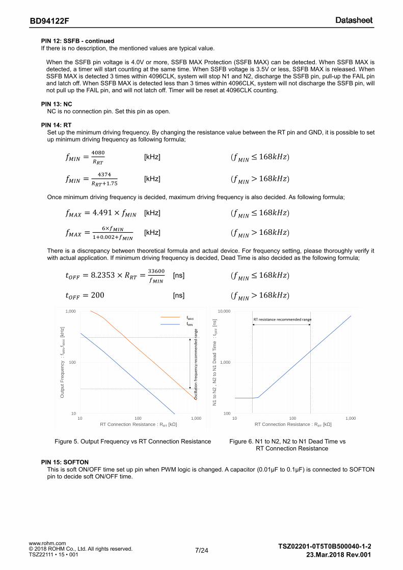
PIN 14: RT
Set up the minimum driving frequency. By changing the resistance value between the RT pin and GND, it is possible to set up minimum driving frequency as following formula;
𝑓𝑀𝐼𝑁 =4080
𝑅𝑅𝑇 [kHz] (𝑓𝑀𝐼𝑁 ≤ 168𝑘𝐻𝑧)
𝑓𝑀𝐼𝑁 =4374
𝑅𝑅𝑇+1.75 [kHz] (𝑓𝑀𝐼𝑁 > 168𝑘𝐻𝑧)
Once minimum driving frequency is decided, maximum driving frequency is also decided. As following formula;
𝑓𝑀𝐴𝑋 = 4.491 × 𝑓𝑀𝐼𝑁 [kHz] (𝑓𝑀𝐼𝑁 ≤ 168𝑘𝐻𝑧)
𝑓𝑀𝐴𝑋 =6×𝑓𝑀𝐼𝑁
1+0.002+𝑓𝑀𝐼𝑁 [kHz] (𝑓𝑀𝐼𝑁 > 168𝑘𝐻𝑧)
There is a discrepancy between theoretical formula and actual device. For frequency setting, please thoroughly verify it with actual application. If minimum driving frequency is decided, Dead Time is also decided as the following formula;
𝑡𝑂𝐹𝐹 = 8.2353 × 𝑅𝑅𝑇 =33600
𝑓𝑀𝐼𝑁 [ns] (𝑓𝑀𝐼𝑁 ≤ 168𝑘𝐻𝑧)
𝑡𝑂𝐹𝐹 = 200 [ns] (𝑓𝑀𝐼𝑁 > 168𝑘𝐻𝑧)
Figure 5. Output Frequency vs RT Connection Resistance Figure 6. N1 to N2, N2 to N1 Dead Time vs RT Connection Resistance
PIN 15: SOFTON
This is soft ON/OFF time set up pin when PWM logic is changed. A capacitor (0.01µF to 0.1µF) is connected to SOFTON pin to decide soft ON/OFF time.
10
100
1,000
10 100 1,000
Ou
tpu
tF
requ
en
cy
:f M
IN,f
MA
X[k
Hz]
RT Connection Resistance : RRT [kΩ]
Osc
illat
ion
freq
uen
cy re
com
men
ded
ran
ge
fMAX
fMIN
100
1,000
10,000
10 100 1,000
N1
to N
2 ,
N2
to N
1 D
ead T
ime
:t O
FF
[ns]
RT Connection Resistance : RRT [kΩ]
RT resistance recommended range
8/24
BD94122F
TSZ02201-0T5T0B500040-1-2
© 2018 ROHM Co., Ltd. All rights reserved. 23.Mar.2018 Rev.001
www.rohm.com
TSZ22111 • 15 • 001
PIN 15: SOFTON - continued
If there is no description, the mentioned values are typical value.
𝑡𝑆𝑂𝐹𝑇𝑂𝑁 = 0.633 × 𝐶𝑆𝑂𝐹𝑇𝑂𝑁 ×𝑉𝑆𝑆𝐹𝐵
𝐼𝑆𝑂𝐹𝑇𝑂𝑁= 0.633 ×
𝐶𝑆𝑂𝐹𝑇𝑂𝑁×𝑉𝑆𝑆𝐹𝐵
1.0×10⁻⁴ [s]
VSSFB is SSFB pin’s voltage. It is decided by system feedback loop.
PIN 16: PGND
This is Power GND pin for output pin N1 and N2 at driver part. Make it independent from the GND pin (Pin 3) on PCB. This pin is not connected to GND pin in IC inside.
PIN 17: N2
This is gate drive output pin for Low Side external FET. Normally connect it to the FET gate through about 10Ω resistor. Internal has 100Ω pull down resistor for noise reduction when STB=L.
PIN 18: N1
This is gate drive output pin for High Side external FET. Normally connect it to the FET gate through about 10Ω resistor. Internal has 100Ω pull down resistor for noise reduction when STB=L.
Detection Condition List of the Protection Functions
If there is no description, the mentioned values are typical value.
Protect Function
Detection pin
Detect Condition
Release Condition Timer
Operation Protection
Type Detection Pin Condition
SSFB
LED OPEN (IS Low Detect)
IS
VIS ≤ 0.1V and
VADIM < 0.55V
VSSFB ≥ 3.5V
VIS > 0.1V and
VADIM < 0.55V
16CLK Latch Off VIS ≤ VADIM/5.5
and 0.55V ≤ VADIM ≤ 2.2V
VIS > VADIM/5.5 and
0.55V ≤ VADIM ≤ 2.2V
VIS ≤ 0.4V and
VADIM > 2.2V
VIS > 0.4V and
VADIM > 2.2V
LED SHORT VOM1 VOM2
VVOMx ≤ VLSPSET
(PDIM=H and
VSSFB ≥ 3.5V) or
(PDIM=H And
LEDOK=H)
VVOMx > VLSPSET 32CLK Latch Off
LED OCP (IS High Detect)
IS VIS ≥ 1.5V - VIS ≤ 1.3V 16CLK Latch Off
OVP VOM1 VOM2
VVOMx ≥ 3.0V - VVOMx ≤ 2.9V 3 times within
4096CLK Latch Off
VCC UVLO VCC VCC ≤ 7.5V - VCC ≥ 8.0V - Restart by Release
SSFB MAX SSFB - VSSFB ≥ 4.0V VSSFB ≤ 3.5V 3 times within
4096CLK Latch Off
In order to reset the latch off condition, to set the STB pin to low or detection of VCCUVLO is required. The count number in the list is calculated with output
driving frequency.
Operation List of the Protection Function
Protect Function Operation of the Protect Function
N1, N2 Output SSFB Pin FAIL Output
LED OPEN Stop after latch Low after latch High after latch
LED SHORT Stop after latch Low after latch High after latch
LED OCP Stop after latch Low after latch High after latch
OVP Stop immediately Low after latch High after latch
VCC UVLO Stop immediately Low immediately High immediately
SSFB MAX Stop after latch Low after latch High after latch
9/24
BD94122F
TSZ02201-0T5T0B500040-1-2
© 2018 ROHM Co., Ltd. All rights reserved. 23.Mar.2018 Rev.001
www.rohm.com
TSZ22111 • 15 • 001
Absolute Maximum Ratings (Ta=25°C)
Parameter Symbol Rating Unit
Power Supply Voltage VCC -0.3 to +18 V
STB, PWM2DC, N2, N1, LSPSET, FAIL, PDIM, ADIM, VOM1, VOM2 Pin Voltage
VSTB, VPWM2DC, VN2, VN1, VLSPSET, VFAIL, VPDIM, VADIM, VVOM1, VVOM2
-0.3 to +18 V
RT, SSFB, IS, SOFTON Pin Voltage VRT, VSSFB, VIS, VSOFTON -0.3 to +5.5 V
Maximum Junction Temperature Tjmax 150 °C
Storage Temperature Range Tstg -55 to +150 °C
Caution 1: Operating the IC over the absolute maximum ratings may damage the IC. The damage can either be a short circuit between pins or an open circuit between pins and the internal circuitry. Therefore, it is important to consider circuit protection measures, such as adding a fuse, in case the IC is operated over the absolute maximum ratings.
Caution 2: Should by any chance the maximum junction temperature rating be exceeded the rise in temperature of the chip may result in deterioration of the properties of the chip. In case of exceeding this absolute maximum rating, design a PCB boards with thermal resistance taken into consideration by increasing board size and copper area so as not to exceed the maximum junction temperature rating.
Thermal Resistance(Note 1)
Parameter Symbol Thermal Resistance (Typ)
Unit 1s(Note 3) 2s2p(Note 4)
SOP18
Junction to Ambient θJA 179.3 119.9 °C/W
Junction to Top Characterization Parameter(Note 2) ΨJT 20 17 °C/W
(Note 1) Based on JESD51-2A(Still-Air). (Note 2) The thermal characterization parameter to report the difference between junction temperature and the temperature at the top center of the outside surface
of the component package. (Note 3) Using a PCB board based on JESD51-3. (Note 4) Using a PCB board based on JESD51-7.
Layer Number of Measurement Board
Material Board Size
Single FR-4 114.3 mm x 76.2 mm x 1.57 mmt
Top
Copper Pattern Thickness
Footprints and Traces 70 μm
Layer Number of Measurement Board
Material Board Size
4 Layers FR-4 114.3 mm x 76.2 mm x 1.6 mmt
Top 2 Internal Layers Bottom
Copper Pattern Thickness Copper Pattern Thickness Copper Pattern Thickness
Footprints and Traces 70 μm 74.2 mm x 74.2 mm 35 μm 74.2 mm x 74.2 mm 70 μm
10/24
BD94122F
TSZ02201-0T5T0B500040-1-2
© 2018 ROHM Co., Ltd. All rights reserved. 23.Mar.2018 Rev.001
www.rohm.com
TSZ22111 • 15 • 001
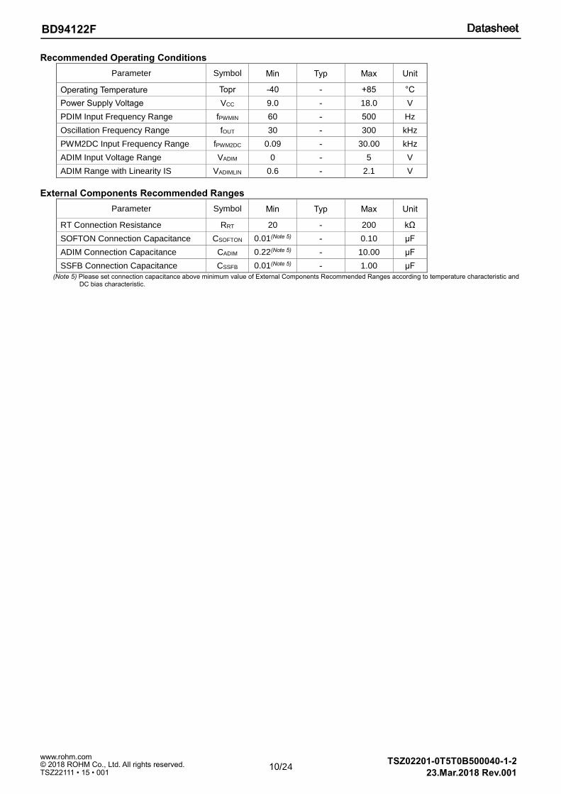
Recommended Operating Conditions
Parameter Symbol Min Typ Max Unit
Operating Temperature Topr -40 - +85 °C
Power Supply Voltage VCC 9.0 - 18.0 V
PDIM Input Frequency Range fPWMIN 60 - 500 Hz
Oscillation Frequency Range fOUT 30 - 300 kHz
PWM2DC Input Frequency Range fPWM2DC 0.09 - 30.00 kHz
ADIM Input Voltage Range VADIM 0 - 5 V
ADIM Range with Linearity IS VADIMLIN 0.6 - 2.1 V
External Components Recommended Ranges
Parameter Symbol Min Typ Max Unit
RT Connection Resistance RRT 20 - 200 kΩ
SOFTON Connection Capacitance CSOFTON 0.01(Note 5) - 0.10 µF
ADIM Connection Capacitance CADIM 0.22(Note 5) - 10.00 µF
SSFB Connection Capacitance CSSFB 0.01(Note 5) - 1.00 µF
(Note 5) Please set connection capacitance above minimum value of External Components Recommended Ranges according to temperature characteristic and DC bias characteristic.
11/24
BD94122F
TSZ02201-0T5T0B500040-1-2
© 2018 ROHM Co., Ltd. All rights reserved. 23.Mar.2018 Rev.001
www.rohm.com
TSZ22111 • 15 • 001
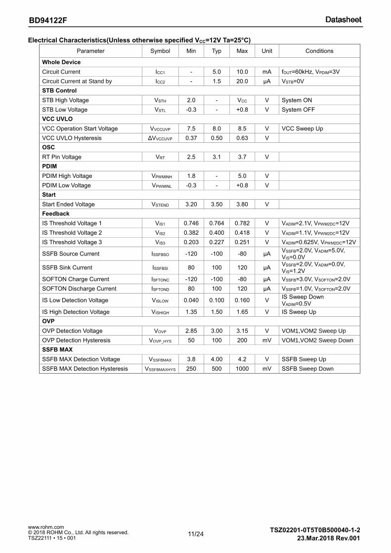
Electrical Characteristics(Unless otherwise specified VCC=12V Ta=25°C)
Parameter Symbol Min Typ Max Unit Conditions
Whole Device
Circuit Current ICC1 - 5.0 10.0 mA fOUT=60kHz, VPDIM=3V
Circuit Current at Stand by ICC2 - 1.5 20.0 µA VSTB=0V
STB Control
STB High Voltage VSTH 2.0 - VCC V System ON
STB Low Voltage VSTL -0.3 - +0.8 V System OFF
VCC UVLO
VCC Operation Start Voltage VVCCUVP 7.5 8.0 8.5 V VCC Sweep Up
VCC UVLO Hysteresis ΔVVCCUVP 0.37 0.50 0.63 V
OSC
RT Pin Voltage VRT 2.5 3.1 3.7 V
PDIM
PDIM High Voltage VPWMINH 1.8 - 5.0 V
PDIM Low Voltage VPWMINL -0.3 - +0.8 V
Start
Start Ended Voltage VSTEND 3.20 3.50 3.80 V
Feedback
IS Threshold Voltage 1 VIS1 0.746 0.764 0.782 V VADIM=2.1V, VPWM2DC=12V
IS Threshold Voltage 2 VIS2 0.382 0.400 0.418 V VADIM=1.1V, VPWM2DC=12V
IS Threshold Voltage 3 VIS3 0.203 0.227 0.251 V VADIM=0.625V, VPWM2DC=12V
SSFB Source Current ISSFBSO -120 -100 -80 µA VSSFB=2.0V, VADIM=5.0V, VIS=0.0V
SSFB Sink Current ISSFBSI 80 100 120 µA VSSFB=2.0V, VADIM=0.0V, VIS=1.2V
SOFTON Charge Current ISFTONC -120 -100 -80 µA VSSFB=3.0V, VSOFTON=2.0V
SOFTON Discharge Current ISFTOND 80 100 120 µA VSSFB=1.0V, VSOFTON=2.0V
IS Low Detection Voltage VISLOW 0.040 0.100 0.160 V IS Sweep Down VADIM=0.5V
IS High Detection Voltage VISHIGH 1.35 1.50 1.65 V IS Sweep Up
OVP
OVP Detection Voltage VOVP 2.85 3.00 3.15 V VOM1,VOM2 Sweep Up
OVP Detection Hysteresis VOVP_HYS 50 100 200 mV VOM1,VOM2 Sweep Down
SSFB MAX
SSFB MAX Detection Voltage VSSFBMAX 3.8 4.00 4.2 V SSFB Sweep Up
SSFB MAX Detection Hysteresis VSSFBMAXHYS 250 500 1000 mV SSFB Sweep Down
12/24
BD94122F
TSZ02201-0T5T0B500040-1-2
© 2018 ROHM Co., Ltd. All rights reserved. 23.Mar.2018 Rev.001
www.rohm.com
TSZ22111 • 15 • 001
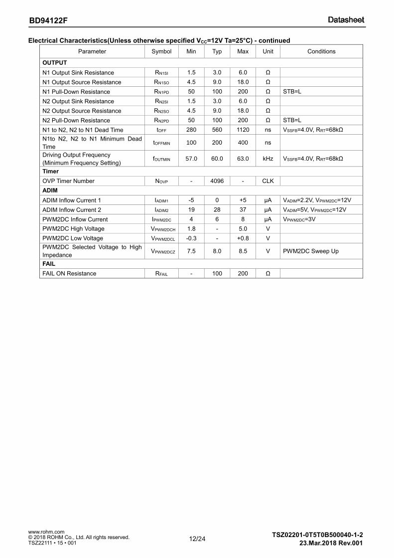
Electrical Characteristics(Unless otherwise specified VCC=12V Ta=25°C) - continued
Parameter Symbol Min Typ Max Unit Conditions
OUTPUT
N1 Output Sink Resistance RN1SI 1.5 3.0 6.0 Ω
N1 Output Source Resistance RN1SO 4.5 9.0 18.0 Ω
N1 Pull-Down Resistance RN1PD 50 100 200 Ω STB=L
N2 Output Sink Resistance RN2SI 1.5 3.0 6.0 Ω
N2 Output Source Resistance RN2SO 4.5 9.0 18.0 Ω
N2 Pull-Down Resistance RN2PD 50 100 200 Ω STB=L
N1 to N2, N2 to N1 Dead Time tOFF 280 560 1120 ns VSSFB=4.0V, RRT=68kΩ
N1to N2, N2 to N1 Minimum Dead
Time tOFFMIN 100 200 400 ns
Driving Output Frequency
(Minimum Frequency Setting) fOUTMIN 57.0 60.0 63.0 kHz VSSFB=4.0V, RRT=68kΩ
Timer
OVP Timer Number NOVP - 4096 - CLK
ADIM
ADIM Inflow Current 1 IADIM1 -5 0 +5 µA VADIM=2.2V, VPWM2DC=12V
ADIM Inflow Current 2 IADIM2 19 28 37 µA VADIM=5V, VPWM2DC=12V
PWM2DC Inflow Current IPWM2DC 4 6 8 µA VPWM2DC=3V
PWM2DC High Voltage VPWM2DCH 1.8 - 5.0 V
PWM2DC Low Voltage VPWM2DCL -0.3 - +0.8 V
PWM2DC Selected Voltage to High
Impedance VPWM2DCZ 7.5 8.0 8.5 V PWM2DC Sweep Up
FAIL
FAIL ON Resistance RFAIL - 100 200 Ω
13/24
BD94122F
TSZ02201-0T5T0B500040-1-2
© 2018 ROHM Co., Ltd. All rights reserved. 23.Mar.2018 Rev.001
www.rohm.com
TSZ22111 • 15 • 001
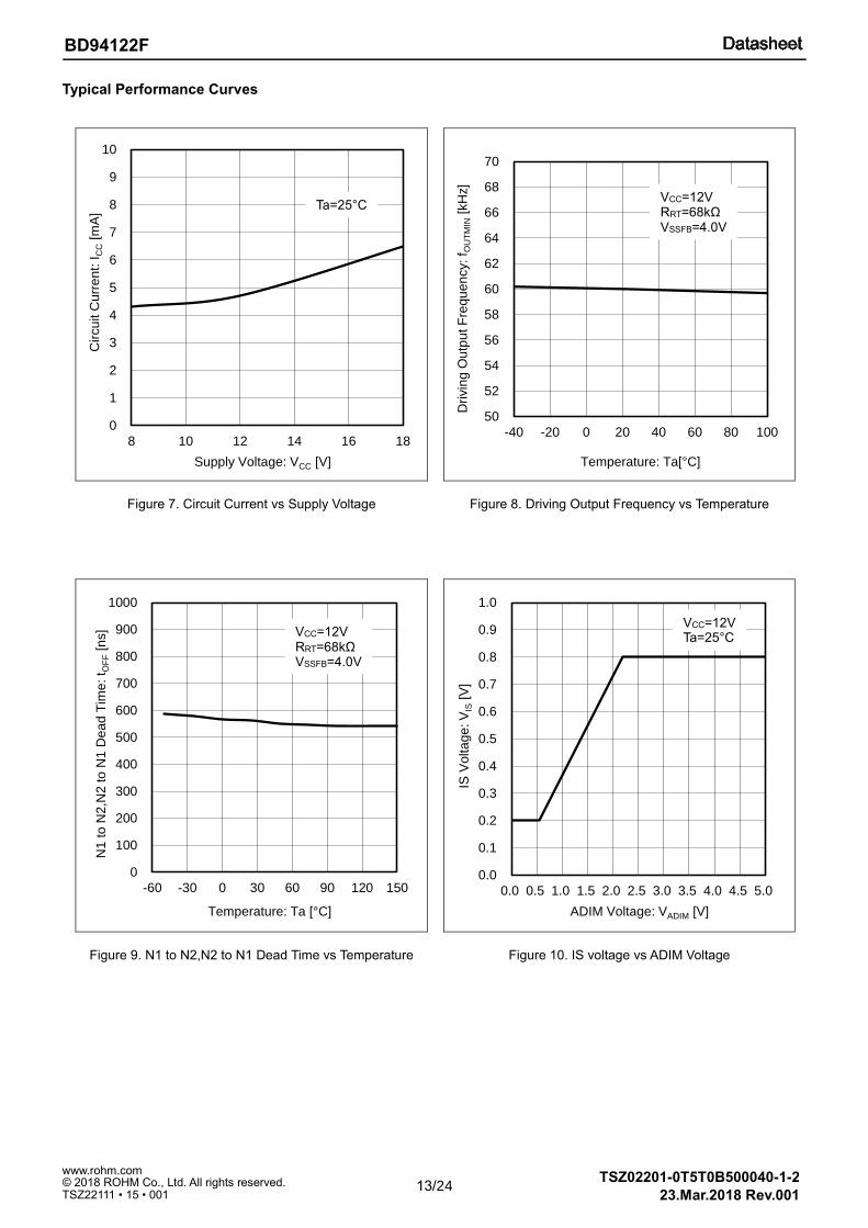
Typical Performance Curves
Figure 7. Circuit Current vs Supply Voltage
Figure 8. Driving Output Frequency vs Temperature
Figure 9. N1 to N2,N2 to N1 Dead Time vs Temperature
Figure 10. IS voltage vs ADIM Voltage
0
1
2
3
4
5
6
7
8
9
10
8 10 12 14 16 18
Cir
cu
it C
urr
en
t: I
CC
[mA
]
Supply Voltage: VCC [V]
50
52
54
56
58
60
62
64
66
68
70
-40 -20 0 20 40 60 80 100
Dri
vin
g O
utp
ut F
req
ue
ncy: f O
UT
MIN
[kH
z]
Temperature: Ta[°C]
0
100
200
300
400
500
600
700
800
900
1000
-60 -30 0 30 60 90 120 150
N1 t
o N
2,N
2 to
N1
De
ad
Tim
e: t O
FF
[ns]
Temperature: Ta [°C]
0.0
0.1
0.2
0.3
0.4
0.5
0.6
0.7
0.8
0.9
1.0
0.0 0.5 1.0 1.5 2.0 2.5 3.0 3.5 4.0 4.5 5.0
IS V
olta
ge
: V
IS[V
]
ADIM Voltage: VADIM [V]
Ta=25°C VCC=12V RRT=68kΩ VSSFB=4.0V
VCC=12V RRT=68kΩ VSSFB=4.0V
VCC=12V Ta=25°C
14/24
BD94122F
TSZ02201-0T5T0B500040-1-2
© 2018 ROHM Co., Ltd. All rights reserved. 23.Mar.2018 Rev.001
www.rohm.com
TSZ22111 • 15 • 001
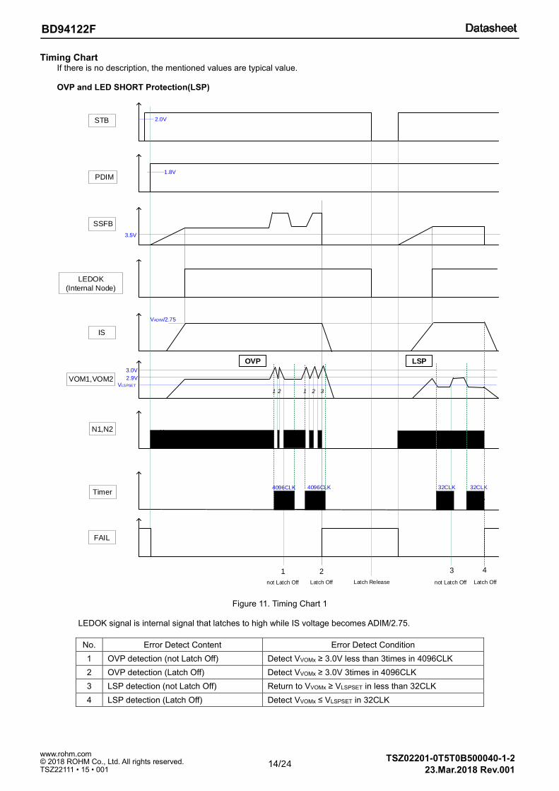
Timing Chart If there is no description, the mentioned values are typical value.
OVP and LED SHORT Protection(LSP)
Figure 11. Timing Chart 1
LEDOK signal is internal signal that latches to high while IS voltage becomes ADIM/2.75.
No. Error Detect Content Error Detect Condition
1 OVP detection (not Latch Off) Detect VVOMx ≥ 3.0V less than 3times in 4096CLK
2 OVP detection (Latch Off) Detect VVOMx ≥ 3.0V 3times in 4096CLK
3 LSP detection (not Latch Off) Return to VVOMx ≥ VLSPSET in less than 32CLK
4 LSP detection (Latch Off) Detect VVOMx ≤ VLSPSET in 32CLK
STB
N1,N2
Timer
FAIL
3.0V
VADIM/2.75
2.0V
PDIM
SSFB
IS
VOM1,VOM2
1.8V
VLSPSET
2.9V
4096CLK 4096CLK 32CLK 32CLK
1 2 1 2 3
1 2 3 4
OVP LSP
not Latch Off Latch Release
3.5V
Latch Off not Latch Off Latch Off
LEDOK
(Internal Node)
15/24
BD94122F
TSZ02201-0T5T0B500040-1-2
© 2018 ROHM Co., Ltd. All rights reserved. 23.Mar.2018 Rev.001
www.rohm.com
TSZ22111 • 15 • 001
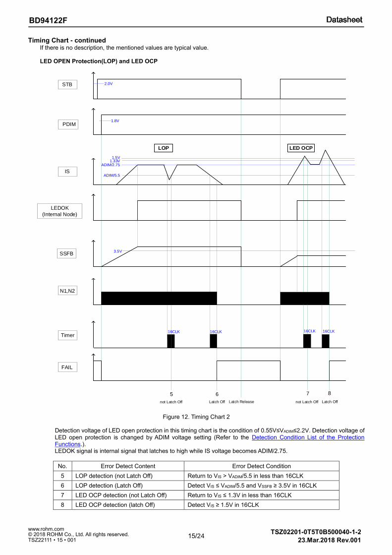
Timing Chart - continued If there is no description, the mentioned values are typical value.
LED OPEN Protection(LOP) and LED OCP
Figure 12. Timing Chart 2 Detection voltage of LED open protection in this timing chart is the condition of 0.55V≤VADIM≤2.2V. Detection voltage of
LED open protection is changed by ADIM voltage setting (Refer to the Detection Condition List of the Protection Functions.). LEDOK signal is internal signal that latches to high while IS voltage becomes ADIM/2.75.
No. Error Detect Content Error Detect Condition
5 LOP detection (not Latch Off) Return to VIS > VADIM/5.5 in less than 16CLK
6 LOP detection (Latch Off) Detect VIS ≤ VADIM/5.5 and VSSFB ≥ 3.5V in 16CLK
7 LED OCP detection (not Latch Off) Return to VIS ≤ 1.3V in less than 16CLK
8 LED OCP detection (latch Off) Detect VIS ≥ 1.5V in 16CLK
STB
N1,N2
Timer
FAIL
ADIM/5.5
ADIM/2.75
2.0V
PDIM
IS
1.8V
1.5V
16CLK 16CLK
1.33V
16CLK 16CLK
SSFB3.5V
5 6 7 8
not Latch Off Latch ReleaseLatch Off not Latch Off Latch Off
LEDOK
(Internal Node)
LED OCPLOP
16/24
BD94122F
TSZ02201-0T5T0B500040-1-2
© 2018 ROHM Co., Ltd. All rights reserved. 23.Mar.2018 Rev.001
www.rohm.com
TSZ22111 • 15 • 001
Timing Chart - continued If there is no description, the mentioned values are typical value.
SSFB MAX Protection
Figure 13. Timing Chart 3
No. Error Detect Content Error Detect Condition
9 SSFB MAX detection (not Latch Off) Detect VSSFB ≥ 4.0V less than 3times in 4096CLK
10 SSFB MAX detection (Latch Off) Detect VSSFB ≥ 4.0V 3times in 4096CLK
STB
N1,N2
FAIL
4.0V
VADIM/2.75
2.0V
PDIM
IS
SSFB
1.8V
3.5V
4096CLK 4096CLK
1 2 1 2 3
9 10
not Latch Off Latch Off
3.33V
Timer
17/24
BD94122F
TSZ02201-0T5T0B500040-1-2
© 2018 ROHM Co., Ltd. All rights reserved. 23.Mar.2018 Rev.001
www.rohm.com
TSZ22111 • 15 • 001
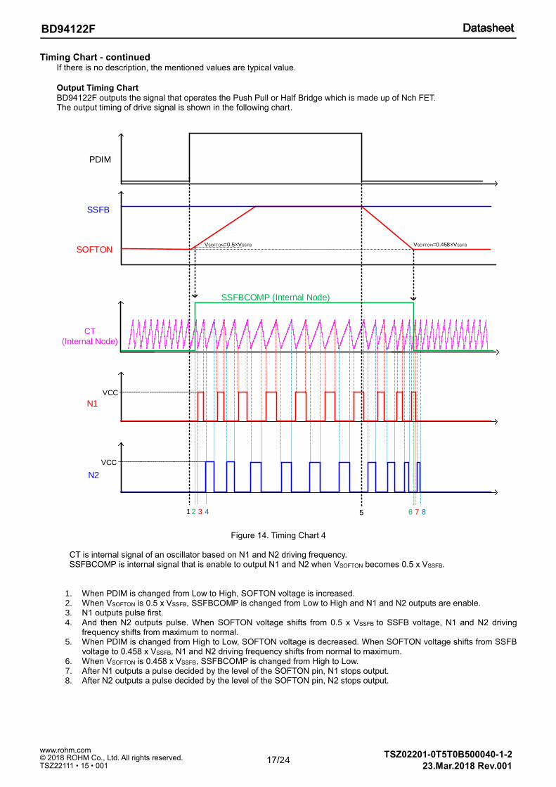
Timing Chart - continued If there is no description, the mentioned values are typical value.
Output Timing Chart
BD94122F outputs the signal that operates the Push Pull or Half Bridge which is made up of Nch FET. The output timing of drive signal is shown in the following chart.
Figure 14. Timing Chart 4 CT is internal signal of an oscillator based on N1 and N2 driving frequency. SSFBCOMP is internal signal that is enable to output N1 and N2 when VSOFTON becomes 0.5 x VSSFB.
1. When PDIM is changed from Low to High, SOFTON voltage is increased. 2. When VSOFTON is 0.5 x VSSFB, SSFBCOMP is changed from Low to High and N1 and N2 outputs are enable. 3. N1 outputs pulse first. 4. And then N2 outputs pulse. When SOFTON voltage shifts from 0.5 x VSSFB to SSFB voltage, N1 and N2 driving
frequency shifts from maximum to normal. 5. When PDIM is changed from High to Low, SOFTON voltage is decreased. When SOFTON voltage shifts from SSFB
voltage to 0.458 x VSSFB, N1 and N2 driving frequency shifts from normal to maximum. 6. When VSOFTON is 0.458 x VSSFB, SSFBCOMP is changed from High to Low. 7. After N1 outputs a pulse decided by the level of the SOFTON pin, N1 stops output. 8. After N2 outputs a pulse decided by the level of the SOFTON pin, N2 stops output.
N2
SSFBCOMP (Internal Node)
N1
VCC
VCC
PDIM
SOFTONVSOFTON=0.5×VSSFB VSOFTON=0.458×VSSFB
CT
(Internal Node)
SSFB
2 3 4 6 7 81 5
18/24
BD94122F
TSZ02201-0T5T0B500040-1-2
© 2018 ROHM Co., Ltd. All rights reserved. 23.Mar.2018 Rev.001
www.rohm.com
TSZ22111 • 15 • 001
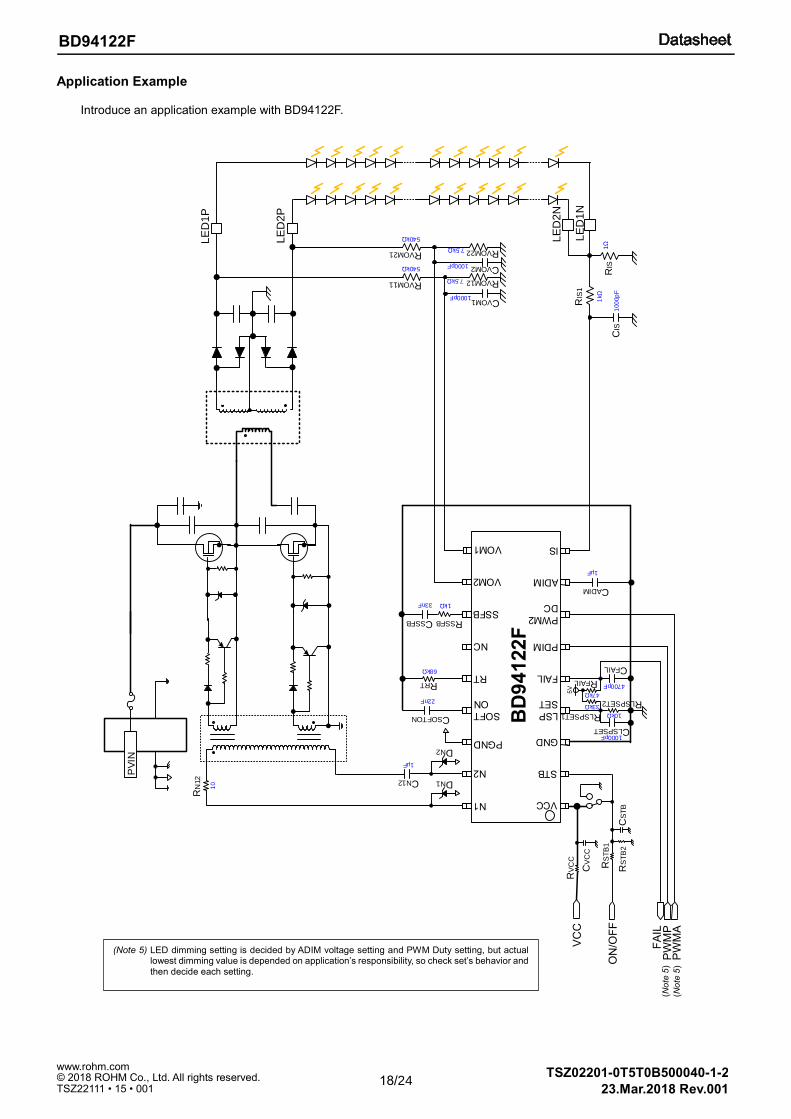
Application Example Introduce an application example with BD94122F.
PV
IN
RV
CC
CV
CC
RS
TB
1
RS
TB
2C
ST
B
CLSPSET
RLSPSET1
RLSPSET2
RFAIL
CFAIL
CADIM
RSSFBCSSFB
RRT
CSOFTON
DN2
DN1
RVOM12
CVOM1
CVOM2
RVOM22
RVOM11
RVOM21
RIS
RIS
1
CIS
LE
D1P
LE
D2P
LE
D2N
LE
D1N
47kΩ
33kΩ
10kΩ
1000pF
4700pF
1µF
68kΩ
22nF
1kΩ33nF
1000pF
1000pF
7.5kΩ
7.5kΩ
540kΩ
540kΩ
1Ω
1kΩ
100
0p
F
CN12
1µF
10
RN
12
(Note 5) LED dimming setting is decided by ADIM voltage setting and PWM Duty setting, but actual lowest dimming value is depended on application’s responsibility, so check set’s behavior and then decide each setting.
19/24
BD94122F
TSZ02201-0T5T0B500040-1-2
© 2018 ROHM Co., Ltd. All rights reserved. 23.Mar.2018 Rev.001
www.rohm.com
TSZ22111 • 15 • 001
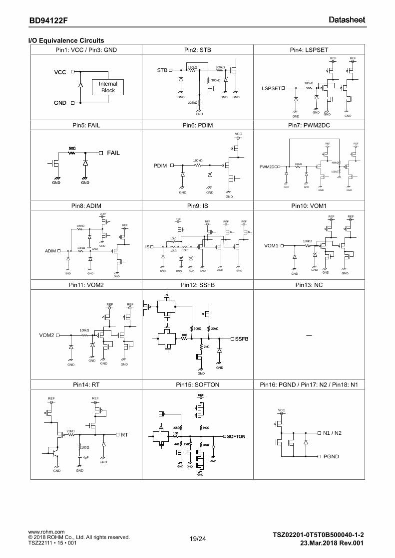
I/O Equivalence Circuits
Pin1: VCC / Pin3: GND Pin2: STB Pin4: LSPSET
VCC
GND
Internal
Block
VCC
GND
Internal
Block
Pin5: FAIL Pin6: PDIM Pin7: PWM2DC
50Ω
GNDGND
FAIL50Ω50Ω
GNDGND
FAIL50Ω
Pin8: ADIM Pin9: IS Pin10: VOM1
Pin11: VOM2 Pin12: SSFB Pin13: NC
SSFB10Ω
GND
GND
500Ω 20kΩ
2kΩ
SSFB10Ω
GND
GND
500Ω 20kΩ
2kΩ
―
Pin14: RT Pin15: SOFTON Pin16: PGND / Pin17: N2 / Pin18: N1
SOFTON10Ω
GND
20kΩ
2kΩ4kΩ
REF
300Ω
200Ω
SOFTON10Ω
GND
20kΩ
2kΩ4kΩ
REF
300Ω
200Ω
GND GND
GND
SOFTON10Ω
GND
20kΩ
2kΩ4kΩ
REF
300Ω
200Ω
GND GND
GND
STB150kΩ
GND
225kΩ
GND
300kΩ
GND
GND
300kΩ
LSPSET100kΩ
GND
GND
REF REF
GNDGND
PDIM
GND GND
GND
VCC
100kΩ
PWM2DC100kΩ
GND GND
GND
REF
GND
REF
100kΩ
400kΩ
ADIM100kΩ
GND GNDGND
REF100kΩ
GND
GND
2.2V
IS10kΩ
GND GND
REF REF
GND
10kΩ
REF
GND
10kΩ
REF
GNDGND
VOM1100kΩ
GND
GND
REF REF
GND GND
VOM2100kΩ
GND
GND
REF REF
GND GND
RT
GND
REFREF
GND
20kΩ
100Ω
GND
4pF
N1 / N2
VCC
PGND
20/24
BD94122F
TSZ02201-0T5T0B500040-1-2
© 2018 ROHM Co., Ltd. All rights reserved. 23.Mar.2018 Rev.001
www.rohm.com
TSZ22111 • 15 • 001
Operational Notes
1. Reverse Connection of Power Supply
Connecting the power supply in reverse polarity can damage the IC. Take precautions against reverse polarity when connecting the power supply, such as mounting an external diode between the power supply and the IC’s power supply pins.
2. Power Supply Lines
Design the PCB layout pattern to provide low impedance supply lines. Furthermore, connect a capacitor to ground at all power supply pins. Consider the effect of temperature and aging on the capacitance value when using electrolytic capacitors.
3. Ground Voltage
Except for pins the output and the input of which were designed to go below ground, ensure that no pins are at a voltage below that of the ground pin at any time, even during transient condition.
4. Ground Wiring Pattern
When using both small-signal and large-current ground traces, the two ground traces should be routed separately but connected to a single ground at the reference point of the application board to avoid fluctuations in the small-signal ground caused by large currents. Also ensure that the ground traces of external components do not cause variations on the ground voltage. The ground lines must be as short and thick as possible to reduce line impedance.
5. Recommended Operating Conditions
The function and operation of the IC are guaranteed within the range specified by the recommended operating conditions. The characteristic values are guaranteed only under the conditions of each item specified by the electrical characteristics.
6. Inrush Current
When power is first supplied to the IC, it is possible that the internal logic may be unstable and inrush current may flow instantaneously due to the internal powering sequence and delays, especially if the IC has more than one power supply. Therefore, give special consideration to power coupling capacitance, power wiring, width of ground wiring, and routing of connections.
7. Operation Under Strong Electromagnetic Field
Operating the IC in the presence of a strong electromagnetic field may cause the IC to malfunction.
8. Testing on Application Boards
When testing the IC on an application board, connecting a capacitor directly to a low-impedance output pin may subject the IC to stress. Always discharge capacitors completely after each process or step. The IC’s power supply should always be turned off completely before connecting or removing it from the test setup during the inspection process. To prevent damage from static discharge, ground the IC during assembly and use similar precautions during transport and storage.
9. Inter-pin Short and Mounting Errors
Ensure that the direction and position are correct when mounting the IC on the PCB. Incorrect mounting may result in damaging the IC. Avoid nearby pins being shorted to each other especially to ground, power supply and output pin. Inter-pin shorts could be due to many reasons such as metal particles, water droplets (in very humid environment) and unintentional solder bridge deposited in between pins during assembly to name a few.
10. Unused Input Pins
Input pins of an IC are often connected to the gate of a MOS transistor. The gate has extremely high impedance and extremely low capacitance. If left unconnected, the electric field from the outside can easily charge it. The small charge acquired in this way is enough to produce a significant effect on the conduction through the transistor and cause unexpected operation of the IC. So unless otherwise specified, unused input pins should be connected to the power supply or ground line.
21/24
BD94122F
TSZ02201-0T5T0B500040-1-2
© 2018 ROHM Co., Ltd. All rights reserved. 23.Mar.2018 Rev.001
www.rohm.com
TSZ22111 • 15 • 001
Operational Notes - continued
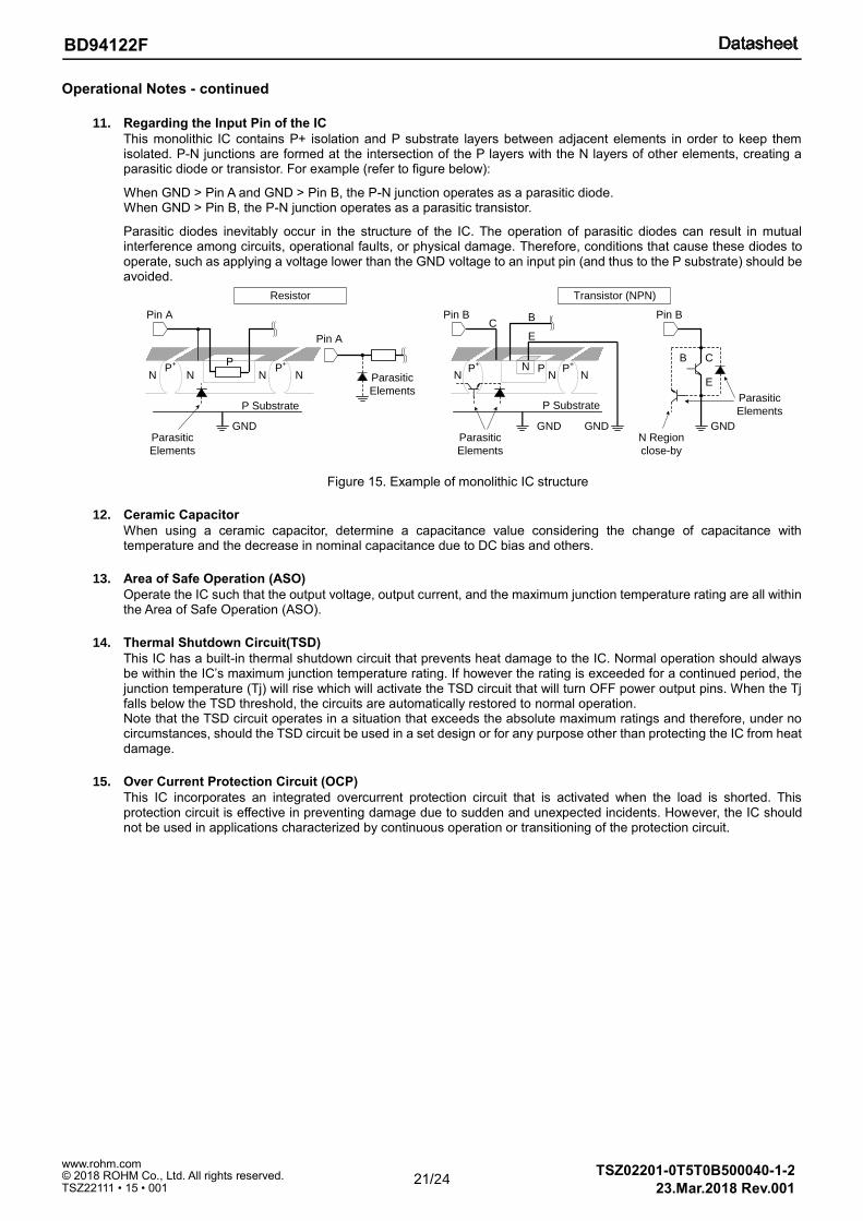
11. Regarding the Input Pin of the IC
This monolithic IC contains P+ isolation and P substrate layers between adjacent elements in order to keep them isolated. P-N junctions are formed at the intersection of the P layers with the N layers of other elements, creating a parasitic diode or transistor. For example (refer to figure below):
When GND > Pin A and GND > Pin B, the P-N junction operates as a parasitic diode. When GND > Pin B, the P-N junction operates as a parasitic transistor.
Parasitic diodes inevitably occur in the structure of the IC. The operation of parasitic diodes can result in mutual interference among circuits, operational faults, or physical damage. Therefore, conditions that cause these diodes to operate, such as applying a voltage lower than the GND voltage to an input pin (and thus to the P substrate) should be avoided.
Figure 15. Example of monolithic IC structure
12. Ceramic Capacitor
When using a ceramic capacitor, determine a capacitance value considering the change of capacitance with temperature and the decrease in nominal capacitance due to DC bias and others.
13. Area of Safe Operation (ASO)
Operate the IC such that the output voltage, output current, and the maximum junction temperature rating are all within the Area of Safe Operation (ASO).
14. Thermal Shutdown Circuit(TSD)
This IC has a built-in thermal shutdown circuit that prevents heat damage to the IC. Normal operation should always be within the IC’s maximum junction temperature rating. If however the rating is exceeded for a continued period, the junction temperature (Tj) will rise which will activate the TSD circuit that will turn OFF power output pins. When the Tj falls below the TSD threshold, the circuits are automatically restored to normal operation. Note that the TSD circuit operates in a situation that exceeds the absolute maximum ratings and therefore, under no circumstances, should the TSD circuit be used in a set design or for any purpose other than protecting the IC from heat damage.
15. Over Current Protection Circuit (OCP)
This IC incorporates an integrated overcurrent protection circuit that is activated when the load is shorted. This protection circuit is effective in preventing damage due to sudden and unexpected incidents. However, the IC should not be used in applications characterized by continuous operation or transitioning of the protection circuit.
N NP
+ P
N NP
+
P Substrate
GND
NP
+
N NP
+N P
P Substrate
GND GND
Parasitic
Elements
Pin A
Pin A
Pin B Pin B
B C
E
Parasitic
Elements
GNDParasitic
Elements
CB
E
Transistor (NPN)Resistor
N Region
close-by
Parasitic
Elements
22/24
BD94122F
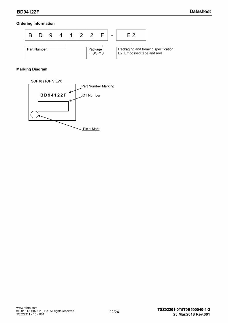
TSZ02201-0T5T0B500040-1-2
© 2018 ROHM Co., Ltd. All rights reserved. 23.Mar.2018 Rev.001
www.rohm.com
TSZ22111 • 15 • 001
Ordering Information
B D 9 4 1 2 2 F - E 2
Part Number Package
F: SOP18 Packaging and forming specification
E2: Embossed tape and reel
Marking Diagram
SOP18 (TOP VIEW)
B D 9 4 1 2 2 F
Part Number Marking
LOT Number
Pin 1 Mark
23/24
BD94122F
TSZ02201-0T5T0B500040-1-2
© 2018 ROHM Co., Ltd. All rights reserved. 23.Mar.2018 Rev.001
www.rohm.com
TSZ22111 • 15 • 001
Physical Dimension and Packing Information
Package Name SOP18
(UNIT: mm) PKG: SOP18 Drawing No.: EX115-5001
(Max 11.55 (include. BURR))
24/24
BD94122F
TSZ02201-0T5T0B500040-1-2
© 2018 ROHM Co., Ltd. All rights reserved. 23.Mar.2018 Rev.001
www.rohm.com
TSZ22111 • 15 • 001
Revision History
Date Revision Changes
23.Mar.2018 001 New Release
Notice-PGA-E Rev.003
© 2015 ROHM Co., Ltd. All rights reserved.
Notice
Precaution on using ROHM Products 1. Our Products are designed and manufactured for application in ordinary electronic equipment (such as AV equipment,
OA equipment, telecommunication equipment, home electronic appliances, amusement equipment, etc.). If you intend to use our Products in devices requiring extremely high reliability (such as medical equipment
(Note 1), transport
equipment, traffic equipment, aircraft/spacecraft, nuclear power controllers, fuel controllers, car equipment including car accessories, safety devices, etc.) and whose malfunction or failure may cause loss of human life, bodily injury or serious damage to property (“Specific Applications”), please consult with the ROHM sales representative in advance. Unless otherwise agreed in writing by ROHM in advance, ROHM shall not be in any way responsible or liable for any damages, expenses or losses incurred by you or third parties arising from the use of any ROHM’s Products for Specific Applications.
(Note1) Medical Equipment Classification of the Specific Applications
JAPAN USA EU CHINA
CLASSⅢ CLASSⅢ
CLASSⅡb CLASSⅢ
CLASSⅣ CLASSⅢ
2. ROHM designs and manufactures its Products subject to strict quality control system. However, semiconductor
products can fail or malfunction at a certain rate. Please be sure to implement, at your own responsibilities, adequate safety measures including but not limited to fail-safe design against the physical injury, damage to any property, which a failure or malfunction of our Products may cause. The following are examples of safety measures:
[a] Installation of protection circuits or other protective devices to improve system safety [b] Installation of redundant circuits to reduce the impact of single or multiple circuit failure
3. Our Products are designed and manufactured for use under standard conditions and not under any special or extraordinary environments or conditions, as exemplified below. Accordingly, ROHM shall not be in any way responsible or liable for any damages, expenses or losses arising from the use of any ROHM’s Products under any special or extraordinary environments or conditions. If you intend to use our Products under any special or extraordinary environments or conditions (as exemplified below), your independent verification and confirmation of product performance, reliability, etc, prior to use, must be necessary:
[a] Use of our Products in any types of liquid, including water, oils, chemicals, and organic solvents [b] Use of our Products outdoors or in places where the Products are exposed to direct sunlight or dust [c] Use of our Products in places where the Products are exposed to sea wind or corrosive gases, including Cl2,
H2S, NH3, SO2, and NO2
[d] Use of our Products in places where the Products are exposed to static electricity or electromagnetic waves [e] Use of our Products in proximity to heat-producing components, plastic cords, or other flammable items [f] Sealing or coating our Products with resin or other coating materials [g] Use of our Products without cleaning residue of flux (even if you use no-clean type fluxes, cleaning residue of
flux is recommended); or Washing our Products by using water or water-soluble cleaning agents for cleaning residue after soldering
[h] Use of the Products in places subject to dew condensation
4. The Products are not subject to radiation-proof design. 5. Please verify and confirm characteristics of the final or mounted products in using the Products. 6. In particular, if a transient load (a large amount of load applied in a short period of time, such as pulse. is applied,
confirmation of performance characteristics after on-board mounting is strongly recommended. Avoid applying power exceeding normal rated power; exceeding the power rating under steady-state loading condition may negatively affect product performance and reliability.
7. De-rate Power Dissipation depending on ambient temperature. When used in sealed area, confirm that it is the use in
the range that does not exceed the maximum junction temperature. 8. Confirm that operation temperature is within the specified range described in the product specification. 9. ROHM shall not be in any way responsible or liable for failure induced under deviant condition from what is defined in
this document.
Precaution for Mounting / Circuit board design 1. When a highly active halogenous (chlorine, bromine, etc.) flux is used, the residue of flux may negatively affect product
performance and reliability.
2. In principle, the reflow soldering method must be used on a surface-mount products, the flow soldering method must be used on a through hole mount products. If the flow soldering method is preferred on a surface-mount products, please consult with the ROHM representative in advance.
For details, please refer to ROHM Mounting specification

Notice-PGA-E Rev.003
© 2015 ROHM Co., Ltd. All rights reserved.
Precautions Regarding Application Examples and External Circuits 1. If change is made to the constant of an external circuit, please allow a sufficient margin considering variations of the
characteristics of the Products and external components, including transient characteristics, as well as static characteristics.
2. You agree that application notes, reference designs, and associated data and information contained in this document
are presented only as guidance for Products use. Therefore, in case you use such information, you are solely responsible for it and you must exercise your own independent verification and judgment in the use of such information contained in this document. ROHM shall not be in any way responsible or liable for any damages, expenses or losses incurred by you or third parties arising from the use of such information.
Precaution for Electrostatic This Product is electrostatic sensitive product, which may be damaged due to electrostatic discharge. Please take proper caution in your manufacturing process and storage so that voltage exceeding the Products maximum rating will not be applied to Products. Please take special care under dry condition (e.g. Grounding of human body / equipment / solder iron, isolation from charged objects, setting of Ionizer, friction prevention and temperature / humidity control).
Precaution for Storage / Transportation 1. Product performance and soldered connections may deteriorate if the Products are stored in the places where:
[a] the Products are exposed to sea winds or corrosive gases, including Cl2, H2S, NH3, SO2, and NO2 [b] the temperature or humidity exceeds those recommended by ROHM [c] the Products are exposed to direct sunshine or condensation [d] the Products are exposed to high Electrostatic
2. Even under ROHM recommended storage condition, solderability of products out of recommended storage time period may be degraded. It is strongly recommended to confirm solderability before using Products of which storage time is exceeding the recommended storage time period.
3. Store / transport cartons in the correct direction, which is indicated on a carton with a symbol. Otherwise bent leads
may occur due to excessive stress applied when dropping of a carton. 4. Use Products within the specified time after opening a humidity barrier bag. Baking is required before using Products of
which storage time is exceeding the recommended storage time period.
Precaution for Product Label A two-dimensional barcode printed on ROHM Products label is for ROHM’s internal use only.
Precaution for Disposition When disposing Products please dispose them properly using an authorized industry waste company.
Precaution for Foreign Exchange and Foreign Trade act Since concerned goods might be fallen under listed items of export control prescribed by Foreign exchange and Foreign trade act, please consult with ROHM in case of export.
Precaution Regarding Intellectual Property Rights 1. All information and data including but not limited to application example contained in this document is for reference
only. ROHM does not warrant that foregoing information or data will not infringe any intellectual property rights or any other rights of any third party regarding such information or data.
2. ROHM shall not have any obligations where the claims, actions or demands arising from the combination of the Products with other articles such as components, circuits, systems or external equipment (including software).
3. No license, expressly or implied, is granted hereby under any intellectual property rights or other rights of ROHM or any third parties with respect to the Products or the information contained in this document. Provided, however, that ROHM will not assert its intellectual property rights or other rights against you or your customers to the extent necessary to manufacture or sell products containing the Products, subject to the terms and conditions herein.
Other Precaution 1. This document may not be reprinted or reproduced, in whole or in part, without prior written consent of ROHM.
2. The Products may not be disassembled, converted, modified, reproduced or otherwise changed without prior written consent of ROHM.
3. In no event shall you use in any way whatsoever the Products and the related technical information contained in the Products or this document for any military purposes, including but not limited to, the development of mass-destruction weapons.
4. The proper names of companies or products described in this document are trademarks or registered trademarks of ROHM, its affiliated companies or third parties.
DatasheetDatasheet
Notice – WE Rev.001© 2015 ROHM Co., Ltd. All rights reserved.
General Precaution 1. Before you use our Products, you are requested to carefully read this document and fully understand its contents.
ROHM shall not be in any way responsible or liable for failure, malfunction or accident arising from the use of any ROHM’s Products against warning, caution or note contained in this document.
2. All information contained in this document is current as of the issuing date and subject to change without any prior
notice. Before purchasing or using ROHM’s Products, please confirm the latest information with a ROHM sales representative.
3. The information contained in this document is provided on an “as is” basis and ROHM does not warrant that all
information contained in this document is accurate and/or error-free. ROHM shall not be in any way responsible or liable for any damages, expenses or losses incurred by you or third parties resulting from inaccuracy or errors of or concerning such information.