Embed Size (px)
Citation preview
This is information on a product in full production.
May 2018 DocID031502 Rev 2 1/82
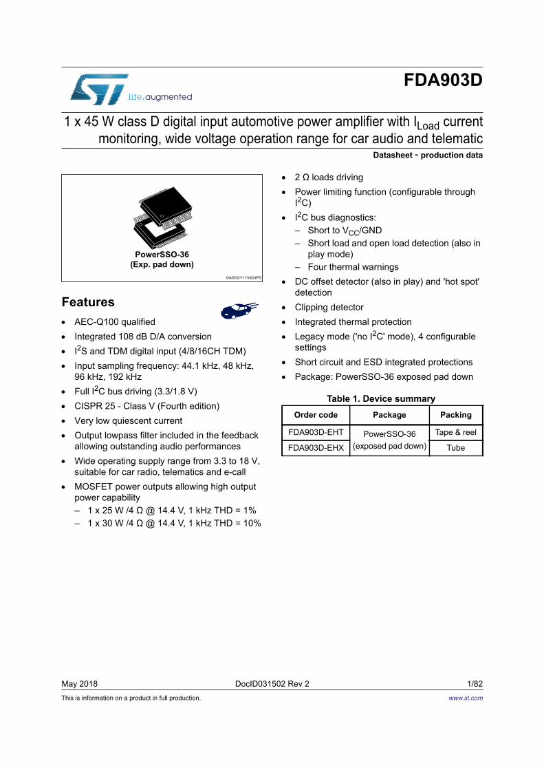
FDA903D
1 x 45 W class D digital input automotive power amplifier with ILoad current monitoring, wide voltage operation range for car audio and telematic
Datasheet - production data
Features AEC-Q100 qualified Integrated 108 dB D/A conversion I2S and TDM digital input (4/8/16CH TDM) Input sampling frequency: 44.1 kHz, 48 kHz,
96 kHz, 192 kHz Full I2C bus driving (3.3/1.8 V) CISPR 25 - Class V (Fourth edition) Very low quiescent current Output lowpass filter included in the feedback
allowing outstanding audio performances Wide operating supply range from 3.3 to 18 V,
suitable for car radio, telematics and e-call MOSFET power outputs allowing high output
power capability– 1 x 25 W /4 Ω @ 14.4 V, 1 kHz THD = 1%– 1 x 30 W /4 Ω @ 14.4 V, 1 kHz THD = 10%
2 Ω loads driving Power limiting function (configurable through
I2C) I2C bus diagnostics:
– Short to VCC/GND– Short load and open load detection (also in
play mode)– Four thermal warnings
DC offset detector (also in play) and 'hot spot' detection
Clipping detector Integrated thermal protection Legacy mode ('no I2C' mode), 4 configurable
settings Short circuit and ESD integrated protections Package: PowerSSO-36 exposed pad down
Table 1. Device summary Order code Package Packing
FDA903D-EHT PowerSSO-36(exposed pad down)
Tape & reel
FDA903D-EHX Tube
www.st.com
Contents FDA903D
2/82 DocID031502 Rev 2
Contents
1 Description . . . . . . . . . . . . . . . . . . . . . . . . . . . . . . . . . . . . . . . . . . . . . . . . . 8
2 Block diagram . . . . . . . . . . . . . . . . . . . . . . . . . . . . . . . . . . . . . . . . . . . . . . 9
3 Pins description . . . . . . . . . . . . . . . . . . . . . . . . . . . . . . . . . . . . . . . . . . . 10
4 Application diagram . . . . . . . . . . . . . . . . . . . . . . . . . . . . . . . . . . . . . . . . 12
5 Electrical specifications . . . . . . . . . . . . . . . . . . . . . . . . . . . . . . . . . . . . . 135.1 Absolute maximum ratings . . . . . . . . . . . . . . . . . . . . . . . . . . . . . . . . . . . . 13
5.2 Thermal data . . . . . . . . . . . . . . . . . . . . . . . . . . . . . . . . . . . . . . . . . . . . . . 13
5.3 Electrical characteristics . . . . . . . . . . . . . . . . . . . . . . . . . . . . . . . . . . . . . . 14
5.4 Typical curves of the main electrical parameters . . . . . . . . . . . . . . . . . . . 17
6 General information . . . . . . . . . . . . . . . . . . . . . . . . . . . . . . . . . . . . . . . . 236.1 LC filter design . . . . . . . . . . . . . . . . . . . . . . . . . . . . . . . . . . . . . . . . . . . . . 23
6.2 Load possibilities . . . . . . . . . . . . . . . . . . . . . . . . . . . . . . . . . . . . . . . . . . . 23
7 Finite state machine . . . . . . . . . . . . . . . . . . . . . . . . . . . . . . . . . . . . . . . . 247.1 Device state and address selection . . . . . . . . . . . . . . . . . . . . . . . . . . . . . 25
7.2 Standby state . . . . . . . . . . . . . . . . . . . . . . . . . . . . . . . . . . . . . . . . . . . . . . 26
7.3 Diagnostic Vcc-Gnd state . . . . . . . . . . . . . . . . . . . . . . . . . . . . . . . . . . . . . 26
7.4 ECO-mode state . . . . . . . . . . . . . . . . . . . . . . . . . . . . . . . . . . . . . . . . . . . . 26
7.5 MUTE-PLAY and diagnostic states . . . . . . . . . . . . . . . . . . . . . . . . . . . . . 27
7.6 Operation compatibility vs battery . . . . . . . . . . . . . . . . . . . . . . . . . . . . . . 28
8 Muting function architecture . . . . . . . . . . . . . . . . . . . . . . . . . . . . . . . . . 298.1 Command dependence . . . . . . . . . . . . . . . . . . . . . . . . . . . . . . . . . . . . . . 29
8.2 Analog-Mute . . . . . . . . . . . . . . . . . . . . . . . . . . . . . . . . . . . . . . . . . . . . . . . 30
8.3 Digital-Mute . . . . . . . . . . . . . . . . . . . . . . . . . . . . . . . . . . . . . . . . . . . . . . . 30
8.4 Mixed mute advantages . . . . . . . . . . . . . . . . . . . . . . . . . . . . . . . . . . . . . . 31
9 Hardware mute pin . . . . . . . . . . . . . . . . . . . . . . . . . . . . . . . . . . . . . . . . . 33
10 Power limiter function . . . . . . . . . . . . . . . . . . . . . . . . . . . . . . . . . . . . . . . 34
DocID031502 Rev 2 3/82
FDA903D Contents
4
10.1 Power limiter control . . . . . . . . . . . . . . . . . . . . . . . . . . . . . . . . . . . . . . . . . 35
11 Diagnostic . . . . . . . . . . . . . . . . . . . . . . . . . . . . . . . . . . . . . . . . . . . . . . . . 3611.1 DC diagnostic . . . . . . . . . . . . . . . . . . . . . . . . . . . . . . . . . . . . . . . . . . . . . . 36
11.1.1 Diagnostic control . . . . . . . . . . . . . . . . . . . . . . . . . . . . . . . . . . . . . . . . . 36
11.1.2 Relation with short circuit protection activation . . . . . . . . . . . . . . . . . . . 37
11.1.3 Load range . . . . . . . . . . . . . . . . . . . . . . . . . . . . . . . . . . . . . . . . . . . . . . . 37
11.2 Short to Vcc / GND diagnostic . . . . . . . . . . . . . . . . . . . . . . . . . . . . . . . . . 38
11.3 Diagnostic time-line diagrams . . . . . . . . . . . . . . . . . . . . . . . . . . . . . . . . . 38
11.4 Open load in play detector . . . . . . . . . . . . . . . . . . . . . . . . . . . . . . . . . . . . 4111.4.1 Open load in play detector operation overview . . . . . . . . . . . . . . . . . . . 41
11.4.2 Processing bandwidth range . . . . . . . . . . . . . . . . . . . . . . . . . . . . . . . . . 41
11.4.3 Audio signal evaluation . . . . . . . . . . . . . . . . . . . . . . . . . . . . . . . . . . . . . 42
11.4.4 Impedance threshold . . . . . . . . . . . . . . . . . . . . . . . . . . . . . . . . . . . . . . . 42
11.4.5 I2C control and timing . . . . . . . . . . . . . . . . . . . . . . . . . . . . . . . . . . . . . . 43
11.5 Input offset detector . . . . . . . . . . . . . . . . . . . . . . . . . . . . . . . . . . . . . . . . . 43
11.6 Output voltage offset detector . . . . . . . . . . . . . . . . . . . . . . . . . . . . . . . . . 44
11.7 Output current offset detector . . . . . . . . . . . . . . . . . . . . . . . . . . . . . . . . . . 4511.7.1 Output current offset detector operation principle . . . . . . . . . . . . . . . . . 45
11.7.2 Result communication and I2C control . . . . . . . . . . . . . . . . . . . . . . . . . 45
11.7.3 Hot spot detection . . . . . . . . . . . . . . . . . . . . . . . . . . . . . . . . . . . . . . . . . 45
11.8 PWM pulse skipping detector . . . . . . . . . . . . . . . . . . . . . . . . . . . . . . . . . . 46
11.9 Thermal protection . . . . . . . . . . . . . . . . . . . . . . . . . . . . . . . . . . . . . . . . . . 47
11.10 Watch-dog . . . . . . . . . . . . . . . . . . . . . . . . . . . . . . . . . . . . . . . . . . . . . . . . 48
11.11 Error frame check . . . . . . . . . . . . . . . . . . . . . . . . . . . . . . . . . . . . . . . . . . . 48
12 Additional features . . . . . . . . . . . . . . . . . . . . . . . . . . . . . . . . . . . . . . . . . 4912.1 AM operation mode . . . . . . . . . . . . . . . . . . . . . . . . . . . . . . . . . . . . . . . . . 49
12.2 Noise gating . . . . . . . . . . . . . . . . . . . . . . . . . . . . . . . . . . . . . . . . . . . . . . . 50
12.3 Dither PWM . . . . . . . . . . . . . . . . . . . . . . . . . . . . . . . . . . . . . . . . . . . . . . . 50
12.4 Real time load current monitoring . . . . . . . . . . . . . . . . . . . . . . . . . . . . . . 5112.4.1 Result communication and I2C control . . . . . . . . . . . . . . . . . . . . . . . . . 51
12.4.2 Current sensing limitations . . . . . . . . . . . . . . . . . . . . . . . . . . . . . . . . . . 52
13 I2S bus interface . . . . . . . . . . . . . . . . . . . . . . . . . . . . . . . . . . . . . . . . . . . 5313.1 I2S standard mode description . . . . . . . . . . . . . . . . . . . . . . . . . . . . . . . . . 54

Contents FDA903D
4/82 DocID031502 Rev 2
13.2 TDM 4CH mode description . . . . . . . . . . . . . . . . . . . . . . . . . . . . . . . . . . . 54
13.3 TDM 8CH mode description . . . . . . . . . . . . . . . . . . . . . . . . . . . . . . . . . . . 55
13.4 TDM 16CH mode description . . . . . . . . . . . . . . . . . . . . . . . . . . . . . . . . . . 56
13.5 Timing requirements . . . . . . . . . . . . . . . . . . . . . . . . . . . . . . . . . . . . . . . . . 57
13.6 Group delay . . . . . . . . . . . . . . . . . . . . . . . . . . . . . . . . . . . . . . . . . . . . . . . 58
14 I2C bus interface . . . . . . . . . . . . . . . . . . . . . . . . . . . . . . . . . . . . . . . . . . . 5914.1 Writing procedure . . . . . . . . . . . . . . . . . . . . . . . . . . . . . . . . . . . . . . . . . . . 60
14.2 Reading procedure . . . . . . . . . . . . . . . . . . . . . . . . . . . . . . . . . . . . . . . . . . 60
14.3 Data validity . . . . . . . . . . . . . . . . . . . . . . . . . . . . . . . . . . . . . . . . . . . . . . . 61
14.4 Start and stop conditions . . . . . . . . . . . . . . . . . . . . . . . . . . . . . . . . . . . . . 61
14.5 Byte format . . . . . . . . . . . . . . . . . . . . . . . . . . . . . . . . . . . . . . . . . . . . . . . . 61
14.6 Acknowledge . . . . . . . . . . . . . . . . . . . . . . . . . . . . . . . . . . . . . . . . . . . . . . 61
14.7 I2C timing . . . . . . . . . . . . . . . . . . . . . . . . . . . . . . . . . . . . . . . . . . . . . . . . . 62
14.8 I2S, I2C and Enable relationship . . . . . . . . . . . . . . . . . . . . . . . . . . . . . . . . 63
15 I2C register . . . . . . . . . . . . . . . . . . . . . . . . . . . . . . . . . . . . . . . . . . . . . . . . 6415.1 Instruction bytes- “I00xxxxx” . . . . . . . . . . . . . . . . . . . . . . . . . . . . . . . . . . . 64
15.2 Data bytes - “I01xxxxx” . . . . . . . . . . . . . . . . . . . . . . . . . . . . . . . . . . . . . . . 73
16 Package information . . . . . . . . . . . . . . . . . . . . . . . . . . . . . . . . . . . . . . . . 7716.1 PowerSSO-36 (exposed pad) package information . . . . . . . . . . . . . . . . . 77
16.2 Package marking information . . . . . . . . . . . . . . . . . . . . . . . . . . . . . . . . . . 80
17 Revision history . . . . . . . . . . . . . . . . . . . . . . . . . . . . . . . . . . . . . . . . . . . 81

DocID031502 Rev 2 5/82
FDA903D List of tables
5
List of tables
Table 1. Device summary . . . . . . . . . . . . . . . . . . . . . . . . . . . . . . . . . . . . . . . . . . . . . . . . . . . . . . . . . . 1Table 2. Pins list function . . . . . . . . . . . . . . . . . . . . . . . . . . . . . . . . . . . . . . . . . . . . . . . . . . . . . . . . . 10Table 3. Absolute maximum ratings . . . . . . . . . . . . . . . . . . . . . . . . . . . . . . . . . . . . . . . . . . . . . . . . . 13Table 4. Thermal data - PowerSSO36 slug-down package . . . . . . . . . . . . . . . . . . . . . . . . . . . . . . . 13Table 5. Electrical characteristics . . . . . . . . . . . . . . . . . . . . . . . . . . . . . . . . . . . . . . . . . . . . . . . . . . . 14Table 6. Operation mode . . . . . . . . . . . . . . . . . . . . . . . . . . . . . . . . . . . . . . . . . . . . . . . . . . . . . . . . . 25Table 7. Command dependence. . . . . . . . . . . . . . . . . . . . . . . . . . . . . . . . . . . . . . . . . . . . . . . . . . . . 29Table 8. Power limiter function . . . . . . . . . . . . . . . . . . . . . . . . . . . . . . . . . . . . . . . . . . . . . . . . . . . . . 34Table 9. Open load in play detector impedance and validity thresholds. . . . . . . . . . . . . . . . . . . . . . 42Table 10. I2S Interface timings . . . . . . . . . . . . . . . . . . . . . . . . . . . . . . . . . . . . . . . . . . . . . . . . . . . . . . 57Table 11. Group delay dependency from input sampling frequency. . . . . . . . . . . . . . . . . . . . . . . . . . 58Table 12. I2C bus interface timing. . . . . . . . . . . . . . . . . . . . . . . . . . . . . . . . . . . . . . . . . . . . . . . . . . . . 62Table 13. IB0-ADDR: “I0000000” . . . . . . . . . . . . . . . . . . . . . . . . . . . . . . . . . . . . . . . . . . . . . . . . . . . . 64Table 14. IB1-ADDR: “I0000001” . . . . . . . . . . . . . . . . . . . . . . . . . . . . . . . . . . . . . . . . . . . . . . . . . . . . 65Table 15. IB2-ADDR: “I0000010” . . . . . . . . . . . . . . . . . . . . . . . . . . . . . . . . . . . . . . . . . . . . . . . . . . . . 66Table 16. IB3-ADDR: “I0000011” . . . . . . . . . . . . . . . . . . . . . . . . . . . . . . . . . . . . . . . . . . . . . . . . . . . . 67Table 17. IB4-ADDR: “I0000100” - CDDiag pin configuration. . . . . . . . . . . . . . . . . . . . . . . . . . . . . . . 67Table 18. IB5-ADDR: “I0000101” - CDDiag pin configuration. . . . . . . . . . . . . . . . . . . . . . . . . . . . . . . 68Table 19. IB6-ADDR: “I0000110” . . . . . . . . . . . . . . . . . . . . . . . . . . . . . . . . . . . . . . . . . . . . . . . . . . . . 68Table 20. IB7-ADDR: “I0000111” . . . . . . . . . . . . . . . . . . . . . . . . . . . . . . . . . . . . . . . . . . . . . . . . . . . . 69Table 21. IB8-ADDR: “I0001000” - CHANNEL CONTROLS . . . . . . . . . . . . . . . . . . . . . . . . . . . . . . . 70Table 22. IB9-ADDR: “I0001001” . . . . . . . . . . . . . . . . . . . . . . . . . . . . . . . . . . . . . . . . . . . . . . . . . . . . 70Table 23. IB10-ADDR: “I0001010” . . . . . . . . . . . . . . . . . . . . . . . . . . . . . . . . . . . . . . . . . . . . . . . . . . . 71Table 24. IB11-ADDR: “I0001011” . . . . . . . . . . . . . . . . . . . . . . . . . . . . . . . . . . . . . . . . . . . . . . . . . . . 71Table 25. IB12-ADDR: “I0001100” . . . . . . . . . . . . . . . . . . . . . . . . . . . . . . . . . . . . . . . . . . . . . . . . . . . 71Table 26. IB13-ADDR: “I0001101” . . . . . . . . . . . . . . . . . . . . . . . . . . . . . . . . . . . . . . . . . . . . . . . . . . . 72Table 27. IB14-ADDR: “I0001110” . . . . . . . . . . . . . . . . . . . . . . . . . . . . . . . . . . . . . . . . . . . . . . . . . . . 72Table 28. DB0-ADDR: “I0100000” . . . . . . . . . . . . . . . . . . . . . . . . . . . . . . . . . . . . . . . . . . . . . . . . . . . 73Table 29. DB1-ADDR: “I0100001” . . . . . . . . . . . . . . . . . . . . . . . . . . . . . . . . . . . . . . . . . . . . . . . . . . . 74Table 30. DB2-ADDR:"I0100010" . . . . . . . . . . . . . . . . . . . . . . . . . . . . . . . . . . . . . . . . . . . . . . . . . . . . 74Table 31. DB3-ADDR: “I0100011” DC Diagnostic Error code . . . . . . . . . . . . . . . . . . . . . . . . . . . . . . 75Table 32. DB4-ADDR:"I0100100" - Current Sensing data (10-8) . . . . . . . . . . . . . . . . . . . . . . . . . . . . 75Table 33. DB5-ADDR:"I0100101" - Current Sensing data (7-0) . . . . . . . . . . . . . . . . . . . . . . . . . . . . . 75Table 34. DB6-ADDR:"I0100110" . . . . . . . . . . . . . . . . . . . . . . . . . . . . . . . . . . . . . . . . . . . . . . . . . . . . 76Table 35. PowerSSO-36 exposed pad (D1 and E2 use the option variation B) package
mechanical data . . . . . . . . . . . . . . . . . . . . . . . . . . . . . . . . . . . . . . . . . . . . . . . . . . . . . . . . . 78Table 36. Document revision history. . . . . . . . . . . . . . . . . . . . . . . . . . . . . . . . . . . . . . . . . . . . . . . . . . 81

List of figures FDA903D
6/82 DocID031502 Rev 2
List of figures
Figure 1. Block diagram . . . . . . . . . . . . . . . . . . . . . . . . . . . . . . . . . . . . . . . . . . . . . . . . . . . . . . . . . . . . 9Figure 2. Pins connection diagram. . . . . . . . . . . . . . . . . . . . . . . . . . . . . . . . . . . . . . . . . . . . . . . . . . . 10Figure 3. Application diagram . . . . . . . . . . . . . . . . . . . . . . . . . . . . . . . . . . . . . . . . . . . . . . . . . . . . . . 12Figure 4. Efficiency and power dissipation (Vs = 14.4 V, RL = 1 x 4 Ω, f = 1 kHz sine wave) . . . . . . 17Figure 5. Efficiency and power dissipation (Vs = 14.4 V, RL = 1 x 4 Ω, f = 1 kHz pink noise) . . . . . . 17Figure 6. Efficiency and power dissipation (Vs = 14.4 V, RL = 1 x 2 Ω, f = 1 kHz sine wave) . . . . . . 17Figure 7. Efficiency and power dissipation (Vs = 14.4 V, RL = 1 x 2 Ω, f = 1 kHz pink noise) . . . . . . 17Figure 8. Efficiency and power dissipation (Vs = 14.4 V, RL = 1 x 8 Ω, f = 1 kHz sine wave) . . . . . . 17Figure 9. Efficiency and power dissipation (Vs = 14.4 V, RL = 1 x 8 Ω, f = 1 kHz pink noise) . . . . . . 17Figure 10. Efficiency and power dissipation (Vs = 18 V, RL = 1 x 4 Ω, f = 1 kHz sine wave) . . . . . . . . 18Figure 11. Efficiency and power dissipation (Vs = 18 V, RL = 1 x 4 Ω, f = 1 kHz pink noise). . . . . . . . 18Figure 12. Efficiency and power dissipation (Vs = 16 V, RL = 1 x 2 Ω, f = 1 kHz sine wave) . . . . . . . 18Figure 13. Efficiency and power dissipation (Vs = 16 V, RL = 1 x 2 Ω, f = 1 kHz pink noise). . . . . . . . 18Figure 14. Efficiency and power dissipation (Vs = 18 V, RL = 1 x 8 Ω, f = 1 kHz sine wave) . . . . . . . . 18Figure 15. Efficiency and power dissipation (Vs = 18 V, RL = 1 x 8 Ω, f = 1 kHz pink noise). . . . . . . . 18Figure 16. Efficiency and power dissipation (Vs = 3.3 V, RL = 1 x 4 Ω, f = 1 kHz sine wave) . . . . . . . 19Figure 17. Efficiency and power dissipation (Vs = 3.3 V, RL = 1 x 4 Ω, f = 1 kHz pink noise) . . . . . . . 19Figure 18. Efficiency and power dissipation (Vs = 3.3 V, RL = 1 x 2 Ω, f = 1 kHz sine wave) . . . . . . . 19Figure 19. Efficiency and power dissipation (Vs = 3.3 V, RL = 1 x 2 Ω, f = 1 kHz pink noise) . . . . . . . 19Figure 20. Efficiency and power dissipation (Vs = 3.3 V, RL = 1 x 8 Ω, f = 1 kHz sine wave) . . . . . . . 19Figure 21. Efficiency and power dissipation (Vs = 3.3 V, RL = 1 x 8 Ω, f = 1 kHz pink noise) . . . . . . . 19Figure 22. Output power vs. supply voltage (RL = 4 Ω, sine wave) . . . . . . . . . . . . . . . . . . . . . . . . . . . 20Figure 23. Output power vs. supply voltage (RL = 2 Ω, sine wave) . . . . . . . . . . . . . . . . . . . . . . . . . . . 20Figure 24. Output power vs. supply voltage (RL = 8 Ω, sine wave) . . . . . . . . . . . . . . . . . . . . . . . . . . . 20Figure 25. THD vs. output power (VS = 14.4 V, RL = 4 Ω) . . . . . . . . . . . . . . . . . . . . . . . . . . . . . . . . . . 20Figure 26. THD vs. output power (VS = 14.4 V, RL = 2 Ω) . . . . . . . . . . . . . . . . . . . . . . . . . . . . . . . . . . 20Figure 27. THD vs. output power (VS = 14.4 V, RL = 8 Ω) . . . . . . . . . . . . . . . . . . . . . . . . . . . . . . . . . . 20Figure 28. THD vs. frequency (VS = 14.4 V, RL = 4 Ω, PO = 1 W). . . . . . . . . . . . . . . . . . . . . . . . . . . . 21Figure 29. THD vs. frequency (VS = 14.4 V, RL = 2 Ω, PO = 1 W). . . . . . . . . . . . . . . . . . . . . . . . . . . . 21Figure 30. THD vs. frequency (VS = 14.4 V, RL = 8 Ω, PO = 1 W). . . . . . . . . . . . . . . . . . . . . . . . . . . . 21Figure 31. Frequency response (1 W, RL = 4 Ω, f = 1 kHz) . . . . . . . . . . . . . . . . . . . . . . . . . . . . . . . . . 21Figure 32. Frequency response (1 W, RL = 2 Ω, f = 1 kHz) . . . . . . . . . . . . . . . . . . . . . . . . . . . . . . . . . 21Figure 33. Frequency response (1 W, RL = 8 Ω, f = 1 kHz) . . . . . . . . . . . . . . . . . . . . . . . . . . . . . . . . . 21Figure 34. PSRR vs. frequency . . . . . . . . . . . . . . . . . . . . . . . . . . . . . . . . . . . . . . . . . . . . . . . . . . . . . . 22Figure 35. Quiescent current vs. supply voltage . . . . . . . . . . . . . . . . . . . . . . . . . . . . . . . . . . . . . . . . . 22Figure 36. Dynamic range . . . . . . . . . . . . . . . . . . . . . . . . . . . . . . . . . . . . . . . . . . . . . . . . . . . . . . . . . . 22Figure 37. FFT - Output spectrum (-60 dBFS input signal) . . . . . . . . . . . . . . . . . . . . . . . . . . . . . . . . . 22Figure 38. Finite state machine diagram . . . . . . . . . . . . . . . . . . . . . . . . . . . . . . . . . . . . . . . . . . . . . . . 24Figure 39. Operation vs. battery charge. . . . . . . . . . . . . . . . . . . . . . . . . . . . . . . . . . . . . . . . . . . . . . . . 28Figure 40. Analog-Mute diagram . . . . . . . . . . . . . . . . . . . . . . . . . . . . . . . . . . . . . . . . . . . . . . . . . . . . . 30Figure 41. Digital-Mute diagram. . . . . . . . . . . . . . . . . . . . . . . . . . . . . . . . . . . . . . . . . . . . . . . . . . . . . . 31Figure 42. Mixed mute diagram . . . . . . . . . . . . . . . . . . . . . . . . . . . . . . . . . . . . . . . . . . . . . . . . . . . . . . 31Figure 43. Analog-Mute vs. Mixed-Mute . . . . . . . . . . . . . . . . . . . . . . . . . . . . . . . . . . . . . . . . . . . . . . . 32Figure 44. HWMute pin schematic . . . . . . . . . . . . . . . . . . . . . . . . . . . . . . . . . . . . . . . . . . . . . . . . . . . . 33Figure 45. Response obtained with a limitation corresponding to 80% of the full-scale . . . . . . . . . . . 35Figure 46. Load range detection configured properly setting IB5 d7-d6 . . . . . . . . . . . . . . . . . . . . . . . 37Figure 47. DC diagnostic before turn on . . . . . . . . . . . . . . . . . . . . . . . . . . . . . . . . . . . . . . . . . . . . . . . 38Figure 48. Short to VCC at device turn on . . . . . . . . . . . . . . . . . . . . . . . . . . . . . . . . . . . . . . . . . . . . . . 39
DocID031502 Rev 2 7/82
FDA903D List of figures
7
Figure 49. DC Diagnostic in Mute . . . . . . . . . . . . . . . . . . . . . . . . . . . . . . . . . . . . . . . . . . . . . . . . . . . . 39Figure 50. Short circuit protection activation - Short to VCC . . . . . . . . . . . . . . . . . . . . . . . . . . . . . . . . 40Figure 51. Short Circuit Protection activation due to short across load, short to Vcc/Gnd not present 40Figure 52. Open load in play detector guaranteed thresholds with standard gain setting . . . . . . . . . . 42Figure 53. Open load in play detector guaranteed thresholds with low gain setting . . . . . . . . . . . . . . 42Figure 54. Open load in play detector timing . . . . . . . . . . . . . . . . . . . . . . . . . . . . . . . . . . . . . . . . . . . . 43Figure 55. Output voltage offset detector operation. . . . . . . . . . . . . . . . . . . . . . . . . . . . . . . . . . . . . . . 44Figure 56. Current offset measurement . . . . . . . . . . . . . . . . . . . . . . . . . . . . . . . . . . . . . . . . . . . . . . . . 45Figure 57. Hot spot detection. . . . . . . . . . . . . . . . . . . . . . . . . . . . . . . . . . . . . . . . . . . . . . . . . . . . . . . . 46Figure 58. PWM pulse skipping detector operation . . . . . . . . . . . . . . . . . . . . . . . . . . . . . . . . . . . . . . . 46Figure 59. Thermal attenuation curve . . . . . . . . . . . . . . . . . . . . . . . . . . . . . . . . . . . . . . . . . . . . . . . . . 47Figure 60. PWM switching frequency selection . . . . . . . . . . . . . . . . . . . . . . . . . . . . . . . . . . . . . . . . . . 49Figure 61. LRF effect on PWM output . . . . . . . . . . . . . . . . . . . . . . . . . . . . . . . . . . . . . . . . . . . . . . . . . 49Figure 62. Dither PWM effect on output PWM. . . . . . . . . . . . . . . . . . . . . . . . . . . . . . . . . . . . . . . . . . . 50Figure 63. Current sensing path. . . . . . . . . . . . . . . . . . . . . . . . . . . . . . . . . . . . . . . . . . . . . . . . . . . . . . 51Figure 64. I2S standard mode . . . . . . . . . . . . . . . . . . . . . . . . . . . . . . . . . . . . . . . . . . . . . . . . . . . . . . . 54Figure 65. TDM4 mode . . . . . . . . . . . . . . . . . . . . . . . . . . . . . . . . . . . . . . . . . . . . . . . . . . . . . . . . . . . . 54Figure 66. TDM8 mode . . . . . . . . . . . . . . . . . . . . . . . . . . . . . . . . . . . . . . . . . . . . . . . . . . . . . . . . . . . . 55Figure 67. TDM16 mode . . . . . . . . . . . . . . . . . . . . . . . . . . . . . . . . . . . . . . . . . . . . . . . . . . . . . . . . . . . 56Figure 68. I2S Interface timings . . . . . . . . . . . . . . . . . . . . . . . . . . . . . . . . . . . . . . . . . . . . . . . . . . . . . . 57Figure 69. I2S clock transition timings . . . . . . . . . . . . . . . . . . . . . . . . . . . . . . . . . . . . . . . . . . . . . . . . . 57Figure 70. I2C bus protocol description . . . . . . . . . . . . . . . . . . . . . . . . . . . . . . . . . . . . . . . . . . . . . . . . 59Figure 71. Reading procedure . . . . . . . . . . . . . . . . . . . . . . . . . . . . . . . . . . . . . . . . . . . . . . . . . . . . . . . 60Figure 72. Without/with auto-increment reading procedure . . . . . . . . . . . . . . . . . . . . . . . . . . . . . . . . . 61Figure 73. I2C bus interface timing. . . . . . . . . . . . . . . . . . . . . . . . . . . . . . . . . . . . . . . . . . . . . . . . . . . . 62Figure 74. PowerSSO-36 (exposed pad) package outline. . . . . . . . . . . . . . . . . . . . . . . . . . . . . . . . . . 77Figure 75. PowerSSO-36 (exp. pad) marking information . . . . . . . . . . . . . . . . . . . . . . . . . . . . . . . . . . 80

Description FDA903D
8/82 DocID031502 Rev 2
1 Description
The FDA903D is a single bridge class D amplifier, designed in the most advanced BCD technology, intended for any automotive audio application (car radio, telematics and e-call, noise and tone generators, etc).
The FDA903D integrates a high performance D/A converter together with powerful MOSFET outputs in class D, so it is very compact and powerful, moreover reaches outstanding efficiency performances (90%).
It has a very wide operating range: it can be operated both with standard car battery levels (5.5-18 V operating, compatible to load dump pulse) and with external step-down generated voltages or emergency battery (since it is compatible to minimum 3.3 V operative).
The feedback loop is including the output L-C low-pass filter, allowing superior frequency response linearity and lower distortion.
FDA903D is configurable through I2C bus interface and is integrating a complete diagnostics array specially intended for automotive applications including innovative open load and DC offset detection in play mode.
Thanks to the solutions implemented to solve the EMI problems, the device is intended to be used in the standard single DIN car-radio box together with the tuner.
Moreover FDA903D features a configurable power limiting function, and can be optionally operated under no I2C mode ('legacy mode').

DocID031502 Rev 2 9/82
FDA903D Block diagram
81
2 Block diagram
Figure 1. Block diagram
Pins description FDA903D
10/82 DocID031502 Rev 2
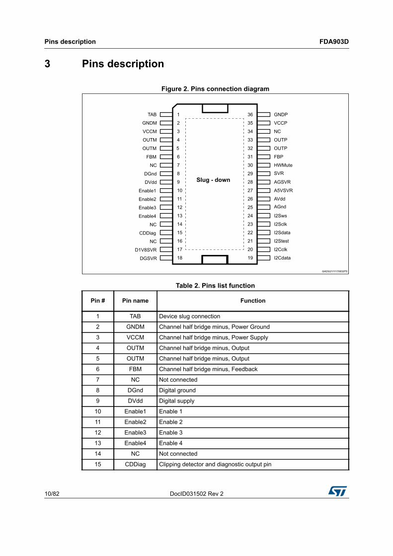
3 Pins description
Figure 2. Pins connection diagram
Table 2. Pins list function
Pin # Pin name Function
1 TAB Device slug connection
2 GNDM Channel half bridge minus, Power Ground
3 VCCM Channel half bridge minus, Power Supply
4 OUTM Channel half bridge minus, Output
5 OUTM Channel half bridge minus, Output
6 FBM Channel half bridge minus, Feedback
7 NC Not connected
8 DGnd Digital ground
9 DVdd Digital supply
10 Enable1 Enable 1
11 Enable2 Enable 2
12 Enable3 Enable 3
13 Enable4 Enable 4
14 NC Not connected
15 CDDiag Clipping detector and diagnostic output pin

DocID031502 Rev 2 11/82
FDA903D Pins description
81
16 NC Not connected
17 D1V8SVR Positive digital supply V(SVR)+0.9V (Internally generated)
18 DGSVR Negative digital supply V(SVR)-0.9V (Internally generated)
19 I2Cdata I2C Data
20 I2Cclk I2C Clock
21 I2Stest test pin, left open
22 I2Sdata I2S/TDM data
23 I2Sclk I2S/TDM Clock input
24 I2Sws I2S/TDM Sync input /Word Select input
25 AGnd Analog ground
26 AVdd Analog supply
27 A5VSVR Positive Analog Supply V(SVR)+2.5V (Internally generated)
28 AGSVR Negative Analog Supply V(SVR)-2.5V (Internally generated)
29 SVR Supply Voltage Ripple Rejection Capacitor
30 HWMute Hardware mute pin
31 FBP Channel half bridge plus, Feedback
32 OUTP Channel half bridge plus, Output
33 OUTP Channel half bridge plus, Output
34 NC Not connected
35 VCCP Channel half bridge plus, Power Supply
36 GNDP Channel half bridge plus, Power Ground
Table 2. Pins list function
Pin # Pin name Function
Application diagram FDA903D
12/82 DocID031502 Rev 2
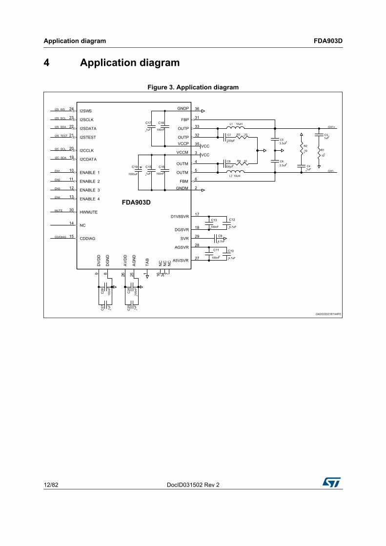
4 Application diagram
Figure 3. Application diagram

DocID031502 Rev 2 13/82
FDA903D Electrical specifications
81
5 Electrical specifications
5.1 Absolute maximum ratings
5.2 Thermal data
Table 3. Absolute maximum ratings Symbol Parameter Value Unit
VCC [VCCP ,VCCM, AVDD, DVDD]
DC supply voltage -0.3 to 28 V
Transient supply voltage for t = 100 ms(1)
1. VCC = 35 V for t < 400 ms as per ISO16750-2 load dump with centralized load dump suppression.
-0.3 to 40 V
GNDmax [DGND, AGND, GNDP, GNDM] Ground pin voltage difference -0.3 to 0.3 V
I2Cdata, I2Cclk I2C bus pins voltage -0.3 to 5.5 V
I2Stest, I2Sdata, I2Sclk, I2Sws I2S bus pins voltage -0.3 to 5.5 V
Enable1,2,3,4 Enables -0.3 to 5.5 V
HWMute Hardware mute -0.3 to 7 V
CDDiag Clip detection -0.3 to 5.5 V
Io Output current (repetitive f > 10 Hz) Internally limited A
Tamb Ambient operating temperature -40 to 125 °C
Tstg, Tj Storage and junction temperature -55 to 150 °C
ESDHBM ESD protection HBM 2000 V
ESDCDM ESD protection CDM 500 V
Table 4. Thermal data - PowerSSO36 slug-down package Symbol Parameter Value Unit
Rth j-a-2s Thermal resistance junction-to-ambient (2s board) 56 °C/W
Rth j-a-2s2p Thermal resistance junction-to-ambient (2s2p board) 31 °C/W
Rth j-a-2s2pv Thermal resistance junction-to-ambient (2s2p+vias) 26 °C/W

Electrical specifications FDA903D
14/82 DocID031502 Rev 2
5.3 Electrical characteristicsVcc = 14.4 V; RL = 4 Ω; f = 1 kHz; Tamb = 25 °C; I2C defaults, unless otherwise specified. LC filter: L = 10 μH, C = 3.3 μF. PWM in In-phase modulation, feedback connected after the filter.
Table 5. Electrical characteristics Symbol Parameter Test condition Min Typ Max Unit
VCC Supply voltage rangeRL = 4 Ω 3.3 - 18 V
RL = 2 Ω (1) 3.3 - 16
IVCC Quiescent current
Device in Standby - 1 5 μA
Device on (MUTE state) - 35 - mA
ECO MODE - 22 - mA
Vos Offset voltage Mute & Play -10 - +10 mV
DVDDDigital supply voltage range - 3.3 - 18 V
AVDDAnalog supply voltage range - 3.3 - 18 V
Iop Overcurrent protection
IB11 D5-4 = 00 9.5 11 12.5 A
IB11 D5-4 = 01 6.7 8 9.3 A
IB11 D5-4 = 10 5 6 7 A
IB11 D5-4 = 11 3 4 5 A
IAVDD Analog current Device on (MUTE state) - 9 20 mA
IDVDD Digital current Device on (MUTE state) - 13 20 mA
- Overvoltage shutdown Attenuation = 0.5 dB(2) 18.5 19.5 20.5 V
VlowMVcc low supply mute threshold
Attenuation <0.5 dB Low voltage mode (IB0D0=1)
2.7 2.9 3.3 V
Attenuation <0.5 dB Standard mode (IB0D0=0)
4.5 4.7 5 V
VhighM Vcc high voltage mute(2) - 18 18.9 20.3 V
UVLOVCCVcc supply UVLO threshold
Standard mode (IB0D0=0) 4.4 4.6 4.8 V
Low voltage mode (IB0D0=1) 2.55 2.7 2.85 V
Tsh Thermal shutdown - 165 175 185 °C
TplThermal protection junction temperature Attenuation = 0.5 dB 150 160 170 °C
Tw1
Thermal warning junction temperature(3)
- - Tpl-5 - °C
Tw2 - - Tpl-15 - °C
Tw3 - - Tpl-35 - °C
Tw4 - - Tpl-50 - °C
DocID031502 Rev 2 15/82
FDA903D Electrical specifications
81
Audio performances
Po Output power
THD = 10 % - 30 - W
THD = 1 % 25 - W
Max power; Vcc = 15.2 V - 50 - W
RL = 2 Ω THD = 10% (1) 55 - W
RL = 2 Ω THD = 1% (1) - 45 - W
RL = 2 Ω, max power(1) - 80 - W
Po Output powerTHD = 10% Vcc = 5 V - 3.8 - W
THD = 10% Vcc = 3.3 V - 1.6 - W
PSRR Power supply rejection ratio f = 1 kHz; Vr = 1Vpk; 70 80 - -
THD Total harmonic distortion PO = 1 W, f = 1 kHz - 0.01 0.05 %
GainStandard gain
at Amplitude = -10 dBFs5.5 5.9 6.3 Vp
Low gain(4) 3.3 3.6 3.9 Vp
DR Dynamic range A-wtd and brickwall 20 kHz filter 102 107.5 - dB
SNR Signal to noise ratio A-wtd and brickwall 20 kHz filter 107 112 - dB
Eout1 Output noise A-wtd and brickwall 20 kHz filter used, no output signal; - 35 55 μV
Eout2 Output noise CCIR 468 filtered - 84 130 μV
ΔVOITUITU Pop filter output voltage
Standby to Mute and Mute to Standby transition -7.5 - +7.5 mV
Mute
VMth(5) Mute pin voltage
threshold
Attenuation <0.5 dB, and digital mute disabled 2.3 - -
VAttenuation ≥60 dB, and digital mute disabled - - 1
IM Mute pin source current - 9 11 13 μA
VMclMute pin internal clamp voltage - 5.5 6 6.5 V
IfeedPeak current flowing in the feedback pins
Standby condition, all feedbacks forced to Vcc, output floating - 110 130 μA
I2C bus interface
fSCL Clock frequency - - - 400 kHz
VIL I2C pins low voltage - - - 0.8 V
VIH I2C pins high voltage - 1.3 - - V
VOLMAX
Maximum I2C data pin low voltage when current Isink is sinked
Isink = 4 mA - 0.12 0.5 V
ILIMAXMaximum input leakage current V = 3.6 V - - 1 μA
Table 5. Electrical characteristics (continued)Symbol Parameter Test condition Min Typ Max Unit
Electrical specifications FDA903D
16/82 DocID031502 Rev 2
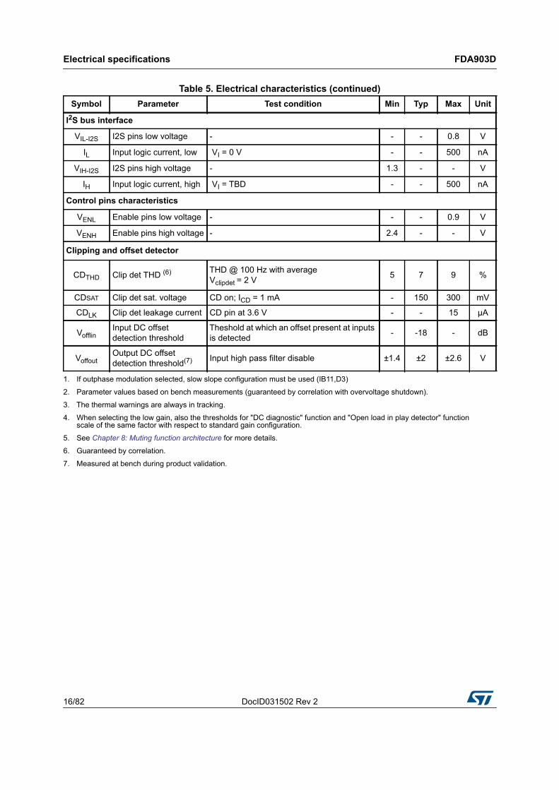
I2S bus interface
VIL-I2S I2S pins low voltage - - - 0.8 V
IL Input logic current, low VI = 0 V - - 500 nA
VIH-I2S I2S pins high voltage - 1.3 - - V
IH Input logic current, high VI = TBD - - 500 nA
Control pins characteristics
VENL Enable pins low voltage - - - 0.9 V
VENH Enable pins high voltage - 2.4 - - V
Clipping and offset detector
CDTHD Clip det THD (6) THD @ 100 Hz with average Vclipdet = 2 V 5 7 9 %
CDSAT Clip det sat. voltage CD on; ICD = 1 mA - 150 300 mV
CDLK Clip det leakage current CD pin at 3.6 V - - 15 μA
VofflinInput DC offset detection threshold
Theshold at which an offset present at inputs is detected - -18 - dB
VoffoutOutput DC offset detection threshold(7) Input high pass filter disable ±1.4 ±2 ±2.6 V
1. If outphase modulation selected, slow slope configuration must be used (IB11,D3)
2. Parameter values based on bench measurements (guaranteed by correlation with overvoltage shutdown).
3. The thermal warnings are always in tracking.
4. When selecting the low gain, also the thresholds for "DC diagnostic" function and "Open load in play detector" function scale of the same factor with respect to standard gain configuration.
5. See Chapter 8: Muting function architecture for more details.
6. Guaranteed by correlation.
7. Measured at bench during product validation.
Table 5. Electrical characteristics (continued)Symbol Parameter Test condition Min Typ Max Unit

DocID031502 Rev 2 17/82
FDA903D Electrical specifications
81
5.4 Typical curves of the main electrical parameters
Figure 4. Efficiency and power dissipation (Vs = 14.4 V, RL = 1 x 4 Ω, f = 1 kHz sine wave)
Figure 5. Efficiency and power dissipation (Vs = 14.4 V, RL = 1 x 4 Ω, f = 1 kHz pink noise)
Figure 6. Efficiency and power dissipation (Vs = 14.4 V, RL = 1 x 2 Ω, f = 1 kHz sine wave)
Figure 7. Efficiency and power dissipation (Vs = 14.4 V, RL = 1 x 2 Ω, f = 1 kHz pink noise)
Figure 8. Efficiency and power dissipation (Vs = 14.4 V, RL = 1 x 8 Ω, f = 1 kHz sine wave)
Figure 9. Efficiency and power dissipation (Vs = 14.4 V, RL = 1 x 8 Ω, f = 1 kHz pink noise)

Electrical specifications FDA903D
18/82 DocID031502 Rev 2
Figure 10. Efficiency and power dissipation (Vs = 18 V, RL = 1 x 4 Ω, f = 1 kHz sine wave)
Figure 11. Efficiency and power dissipation (Vs = 18 V, RL = 1 x 4 Ω, f = 1 kHz pink noise)
Figure 12. Efficiency and power dissipation (Vs = 16 V, RL = 1 x 2 Ω, f = 1 kHz sine wave)
Figure 13. Efficiency and power dissipation (Vs = 16 V, RL = 1 x 2 Ω, f = 1 kHz pink noise)
Figure 14. Efficiency and power dissipation (Vs = 18 V, RL = 1 x 8 Ω, f = 1 kHz sine wave)
Figure 15. Efficiency and power dissipation (Vs = 18 V, RL = 1 x 8 Ω, f = 1 kHz pink noise)

DocID031502 Rev 2 19/82
FDA903D Electrical specifications
81
Figure 16. Efficiency and power dissipation (Vs = 3.3 V, RL = 1 x 4 Ω, f = 1 kHz sine wave)
Figure 17. Efficiency and power dissipation (Vs = 3.3 V, RL = 1 x 4 Ω, f = 1 kHz pink noise)
Figure 18. Efficiency and power dissipation (Vs = 3.3 V, RL = 1 x 2 Ω, f = 1 kHz sine wave)
Figure 19. Efficiency and power dissipation (Vs = 3.3 V, RL = 1 x 2 Ω, f = 1 kHz pink noise)
Figure 20. Efficiency and power dissipation (Vs = 3.3 V, RL = 1 x 8 Ω, f = 1 kHz sine wave)
Figure 21. Efficiency and power dissipation (Vs = 3.3 V, RL = 1 x 8 Ω, f = 1 kHz pink noise)

Electrical specifications FDA903D
20/82 DocID031502 Rev 2
Figure 22. Output power vs. supply voltage (RL = 4 Ω, sine wave)
Figure 23. Output power vs. supply voltage (RL = 2 Ω, sine wave)
Figure 24. Output power vs. supply voltage (RL = 8 Ω, sine wave)
Figure 25. THD vs. output power (VS = 14.4 V, RL = 4 Ω)
Figure 26. THD vs. output power (VS = 14.4 V, RL = 2 Ω)
Figure 27. THD vs. output power (VS = 14.4 V, RL = 8 Ω)
DocID031502 Rev 2 21/82
FDA903D Electrical specifications
81
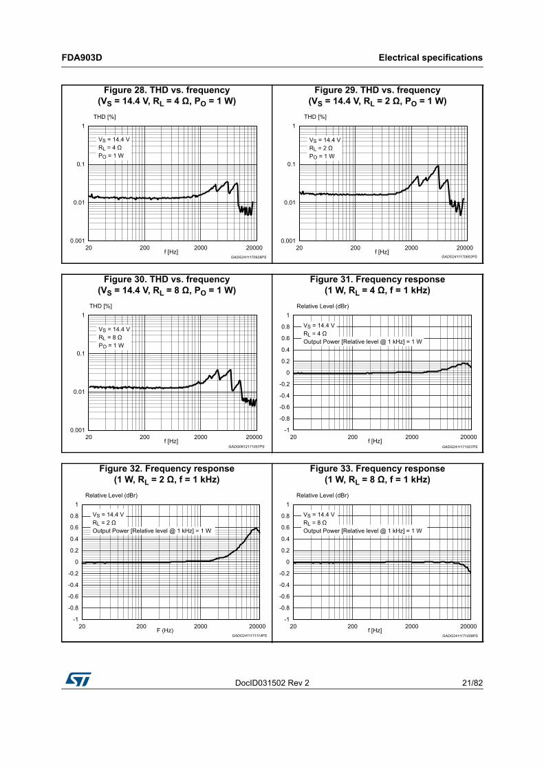
Figure 28. THD vs. frequency (VS = 14.4 V, RL = 4 Ω, PO = 1 W)
Figure 29. THD vs. frequency (VS = 14.4 V, RL = 2 Ω, PO = 1 W)
Figure 30. THD vs. frequency (VS = 14.4 V, RL = 8 Ω, PO = 1 W)
Figure 31. Frequency response (1 W, RL = 4 Ω, f = 1 kHz)
Figure 32. Frequency response (1 W, RL = 2 Ω, f = 1 kHz)
Figure 33. Frequency response (1 W, RL = 8 Ω, f = 1 kHz)

Electrical specifications FDA903D
22/82 DocID031502 Rev 2
Figure 34. PSRR vs. frequency Figure 35. Quiescent current vs. supply voltage
Figure 36. Dynamic range Figure 37. FFT - Output spectrum (-60 dBFS input signal)

DocID031502 Rev 2 23/82
FDA903D General information
81
6 General information
6.1 LC filter design The audio performance of a Class D amplifier are heavily influenced by the characteristics of the output LC filter. The choice of its components is quite critical because a lot of constraints have to be fulfilled at the same time: size, cost, filter for EMI suppression, efficiency. In particular, both the inductor and the capacitor exhibit a non linear behavior: the value of the inductance is a function of the instantaneous current in it and similarly the value of the capacitor is a function of the voltage across it.
In the classical approach, where the feedback loop is closed right at the output of the power stage, the LC filter is placed outside the loop and these nonlinearities cause the Total Harmonic Distortion (THD) to increase. The only way to avoid this phenomenon would be to use components which are highly linear, but this means they are also bigger and/or more expensive.
Furthermore, when the LC filter is outside the loop, its frequency response heavily depends on the impedance of the loudspeaker; this is one of the most critical aspects of Class-D amplifiers. In standard class D this can be mitigated, but not solved, by means of additional damping networks, increasing cost, space and power dissipation. FDA903D, instead, provides a very flat frequency response over audio-band which can not be achieved by standard class D without feedback after LC filter.
Since the demodulator group is now in the feedback path, some constraints regarding the inductor and capacitor choice are still present but of course less stringent than in the case of a typical switching application.
Moreover FDA903D can be used with the 'classical' configuration of feedback on output (before LC filter), through I2C configuration, allowing the maximum flexibility. The choice depends mainly on EMI target /requirements and could slightly affect other performances (like damping factor, or THD).
6.2 Load possibilitiesFDA903D supports several load possibilities, driving 2 Ω, 4 Ω and higher ohmic loads.
Possible channel configurations are: 1 x 4 ohm (or higher) (up to 18 V) 1 x 2 ohm (up to 16 V)

Finite state machine FDA903D
24/82 DocID031502 Rev 2
7 Finite state machine
FDA903D has a finite state machine which manages amplifier functionality, reacting to user and system inputs
Figure 38. Finite state machine diagram

DocID031502 Rev 2 25/82
FDA903D Finite state machine
81
7.1 Device state and address selection Through Enable pins configuration it is possible to select different I2C addresses (up to 8) or to configure the device in 4 different legacy ('no I2C' modes) according to table 6.
In this way, up to 8 devices can be easily used in the same application with a single I2C bus.
Moreover it is possible to work without I2C configuring the voltage range and switching mode to be used.
When a valid combination of Enable 1/2/3/4 is recognized the device turns on all the internal supply voltages and outputs are biased to Vcc/2.
The internal I2C registers are pre-settled in "default condition", waiting for the I2C next instruction.
The return in the Standby condition, (all enable pins at 0), will cause the reset of the amplifier. As defined in the finite state machine, The same event will happen if PLL is not locked, I2S is missing or not correct, Vcc for system reset.
FDA903D can work only in I2C slave mode.
Table 6. Operation mode Enable 1 Enable 2 Enable 3 Enable 4
Stand By 0 0 0 0
Amplifier ON address 1 = ‘1110000’ 0 1 0 0
Amplifier ON address 2 = ‘1110001’ 1 1 0 0
Amplifier ON address 3 = ‘1110010’ 0 0 1 0
Amplifier ON address 4 = ‘1110011’ 0 1 1 0
Amplifier ON address 5 = ‘1110100’ 0 1 0 1
Amplifier ON address 6 = ‘1110101’ 1 1 0 1
Amplifier ON address 7 = ‘1110110’ 0 0 1 1
Amplifier ON address 8 = ‘1110111’ 0 1 1 1
Legacy mode: low voltage mode; in-phase 1 1 1 0
Legacy mode: low voltage mode; out-phase 1 1 1 1
Legacy mode: standard voltage mode; in-phase 1 0 0 0
Legacy mode: standard voltage mode; out-phase 1 0 0 1

Finite state machine FDA903D
26/82 DocID031502 Rev 2
7.2 Standby stateENABLE1, ENABLE2, ENABLE3, ENABLE4 pins have a double function: set of I2C addresses and start-up of the system.
If ENABLE1/2/3/4 are all low, ("000"), then the FDA903D is off, the outputs remain biased to ground and the current consumption is limited to Isb. In this case the FSM is in "Standby" state.
7.3 Diagnostic Vcc-Gnd stateAfter exiting from Stand-By state the device passes through Diagnostic Vcc/Gnd state.
In this state the amplifier checks the presence of the following faults: Shorts to ground or to Vcc; Under-voltage (UVLOVCC); Thermal shutdown
FDA903D will then move to the next state (Eco-mode) only if there isn't any of these faults for at least 90ms, thus avoiding any danger for the amplifier and the user system.
Meanwhile, if a stable fault is present, it will be communicated to the user via I2C after 90 ms, in order to provide always only stable information about the system. In this case the device will not move to Eco-mode, waiting for the fault cause removal
While the amplifier is in Diagnostic Vcc-Gnd state it can receive all the I2C commands, but it will turn-on the PWM only when it enters in the next state: ECO-mode. This procedure prevents wrong or unwanted I2C communication to bring the amplifier into dangerous situation (if a short to Vcc or Gnd is present).
Following conditions will move the amplifier in Diagnostic Vcc-Gnd state from any other functional state: Over current protection trigger UVLOVCC Over voltage (through DUMP condition) Thermal shutdown
7.4 ECO-mode state In ECO-mode state the amplifier is fully operative from a communication point of view and can receive and actuate all the commands given by the user.
In ECO-mode the output switching is disabled, thus allowing low quiescent current consumption and therefore low power dissipation. The device is also able to move from ECO-mode state to MUTE state, turning on the output switching, within about 1 ms - without experiencing POP-noise.
This allows a very fast transition from ECO-mode to PLAY.

DocID031502 Rev 2 27/82
FDA903D Finite state machine
81
7.5 MUTE-PLAY and diagnostic statesThe amplifier can move from ECO-mode state to MUTE state selecting "PWM-ON" via I2C. This operation turns-on the output PWM.
FDA903D can move to PLAY state (from MUTE state) via "PLAY" I2C command and returns to MUTE state from PLAY state acting on the same bit.
Transition time between mute and play states could be selected via I2C.
Some external conditions could lead the amplifier in mute state automatically: Low battery mute High battery mute Thermal mute Hardware pin mute
Once mute condition is no more present the FDA903D will return automatically in PLAY state, following I2C register program set.
Of course the user can decide to change the amplifier programming in the meanwhile, thus avoiding the automatic return in PLAY.
From MUTE state the user can also select to enter DC diagnostic state.

Finite state machine FDA903D
28/82 DocID031502 Rev 2
7.6 Operation compatibility vs batteryThe FDA903D operation compatibility vs the battery value is reported in the figure below.
Figure 39. Operation vs. battery charge
Note: When Overvoltage Shutdown is reached, I2S interface is switched off and relative I/O are maintained in HighZ.

DocID031502 Rev 2 29/82
FDA903D Muting function architecture
81
8 Muting function architecture
FDA903D uses a mixed signal approach for muting function.
Muting function is activated by different "mute command signal": “High voltage mute”: active when Vcc enters in a voltage window over the max voltage;
the window is specified in the electrical parameters table. “Low Battery mute”: active when Vcc enters in a voltage window under the min voltage;
the window is specified in the electrical parameters table. “Hardware mute”: active when HWMute pin enters in the voltage window specified in
the electrical parameters table. Thermal mute”: active when temperature enters in the temperature window over the
max temperature; the window is specified in the electrical parameters table. “I2C Mute”: active user select mute/play I2C bits.
The mute is achieved by the combination of two separated actuators, “Analog-mute” and “Digital-mute”.
8.1 Command dependenceAnalog and digital mute actuators activation could be different based on the mute command signal. This is described in the following table:
Table 7. Command dependence Command signal When? Mute Unmute
Low Battery muteWhen Vcc enters inside
the low battery mute window
Mixed mute. Analog & Digital, at the same
time (1)
1. User can decide to disable Digital-Mute/Unmute using bit IB13-d6; in this case in all the conditions, (except I2C Mute), the Mute/Unmute will be purely Analog.
Digital (1)
High Voltage muteWhen Vcc enters inside the high voltage mute
window
Mixed mute. Analog & Digital, at the same
time (1)Digital (1)
Thermal MuteWhen temperature
enters inside thermal mute window
Analog Analog
Hardware MuteWhen hardware pin
voltage enters inside its mute window
Mixed mute. Analog & Digital, at the same
time(1)Digital (1)
I2C Mute When I2C mute bits are selected Digital Digital

Muting function architecture FDA903D
30/82 DocID031502 Rev 2
8.2 Analog-MuteAnalog-Mute senses when the mute command signal transits across the muting window, and attenuates the output signal proportionally to the command signal level inside the muting window.
Figure 40. Analog-Mute diagram
8.3 Digital-MuteDigital-Mute acts on the digitally elaborated output signal attenuating it gradually to zero with digital steps in a pre-defined time frame (tmute). The muting time, (tmute), can be selected by I2C, (IB6 d7-d6). There are two different actions performed by digital-mute function:
Mute: it starts when any mute command signal, marked as Mixed Mute in Table 7, enters in the muting window. This event rises the Start-Analog-Mute signal, communicated on DB6[4]. The muting ends after tmute, selectable through IB6[7-6]. The Start-Analog-Mute signal is ignored until the muting ramp has ended.
Approximately, the corresponding analog mute attenuation at the beginning of the muting window is 0.5dB.
UnMute: it starts when all the mute commands, marked with Mixed Mute in Table 7, exit from the muting window. This event resets the Start-Analog-Mute signal, communicated on DB6[4]. The unmuting ends after tmute, selectable through IB6[7-6]. The Start-Analog-Mute signal is ignored until the unmuting ramp has ended.

DocID031502 Rev 2 31/82
FDA903D Muting function architecture
81
Figure 41. Digital-Mute diagram
Note: in case of I2C mute the Digital-mute actuation does not follow Analog-mute level but only the I2C command.
8.4 Mixed mute advantagesThe mixed mute approach is the superposition of the two mute actuators, Analog-Mute and Digital-mute, at the same time.
Here below the example of previous pages with mixed mute:
Figure 42. Mixed mute diagram

Muting function architecture FDA903D
32/82 DocID031502 Rev 2
The Mixed-Mute approach is more robust than Analog-Mute only approach. The effects are visible when the command signal variations inside the muting window last longer than the muting/unmuting time. An example is depicted in the figure below:
Figure 43. Analog-Mute vs. Mixed-Mute
In any moment the user can disable the Digital-mute, acting on I2C bit IB13-d6, obtaining the standard Analog-mute function.

DocID031502 Rev 2 33/82
FDA903D Hardware mute pin
81
9 Hardware mute pin
The pin "HWMute" (pin 30) acts as mute command for the channel. The device is muted when this pin is low, while it is in play when this pin is high (low/high threshold in Table 5: Electrical characteristics).
Inside the device, connected to this pin a pull-up current generator puts the device in play if left floating. An internal clamp limits the Mute pin voltage. If not used, this pin should remain floating.
To drive the Mute pin to get a hardware mute an external pull-down open drain is needed. (See Figure 44), RMute must be < 60 kΩ
Figure 44. HWMute pin schematic

Power limiter function FDA903D
34/82 DocID031502 Rev 2
10 Power limiter function
An adjustable power limiting function has been integrated to protect "small speakers" applications: thanks to this feature, it's possible to limit by configuration the max power delivered to the load.
Taking advantage of digital input architecture, the output power limitation is obtained through the management of the input signal. It's important to underline that the limitation is implemented independently of the supply voltage value.
The intervention thresholds, configurable through I2C are listed in the table below
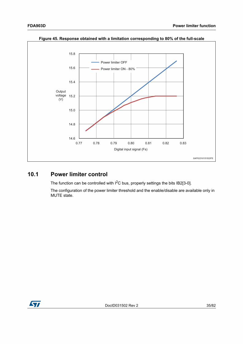
The limitation is gradual in order to have no impact on the acoustic performance. Depending on the signal amplitude and the desired attenuation, different gains are applied to the signal itself.
Here an example of the response obtained with a limitation corresponding to 80% of the full-scale: the blue line represents the signal when the power limiter is not employed, while the red line is the result of the applied attenuation.
Table 8. Power limiter function
I2C IB2[3-0] Full-Scale Voltage limit
Output Voltage limit [V]
Standard gain setting Low gain setting
0000 100% (Disabled) 19 (1)
1. 19 V is only a reference level, coherently with "standard gain" value in Section 5.3, to deduce the power limiter thresholds. The reference level is unreachable due to the maximum supply voltage range, equal to 18 V.
11.4
1011 80% 15.2 9.12
1010 70% 13.3 7.98
1001 60% 11.4 6.84
1000 50% 9.5 5.7
0111 45% 8.55 5.13
0110 40% 7.6 4.56
0101 35% 6.65 3.99
0100 30% 5.7 3.42
0011 25% 4.75 2.85
0010 20% 3.8 2.28
0001 15% 2.85 1.71
DocID031502 Rev 2 35/82
FDA903D Power limiter function
81
Figure 45. Response obtained with a limitation corresponding to 80% of the full-scale
10.1 Power limiter controlThe function can be controlled with I2C bus, properly settings the bits IB2[3-0].
The configuration of the power limiter threshold and the enable/disable are available only in MUTE state.

Diagnostic FDA903D
36/82 DocID031502 Rev 2
11 Diagnostic
The FDA amplifiers family provides diagnostic function for detecting several possible faults conditions.
Any warning information will be stored in the I2C interface and kept until the first I2C bus reading operation. Some fault events can be sent to CDDiag pin as trigger for an interrupt process.
Here reported the faults detectable taking advantage of FDA903D's diagnostic features: Short to VCC/GND; Short or open load (with DC diagnostic); Open load during play; Under/over voltage events; Chip over temperature; Digital input offset; Output voltage offset; Output current offset; Output clipping; Over current.
The fault events are managed with different actions depending on their severity.
It is important, for a correct diagnostic result collection, to clean diagnosis related I2C register and the DB6, to clean eventual Start Analog Mute flag, through a read operation.
11.1 DC diagnosticThe DC diagnostic is a routine performed to detect the load connection status.
FDA amplifiers family provides a highly reliable and noise immune load diagnostic algorithm, in order to prevent false detections induced by supply voltage variations or mechanical stress on the speaker (e.g. car door closing). The algorithm includes the internal generation of a properly calibrated and pop-free test signal.
For an extensive description of the DC diagnostic feature, please refer to the DC Diagnostic user manual.
11.1.1 Diagnostic controlDC diagnostic can be run setting via I2C "Start Diag DC".
Diagnostic signal is generated and test is performed only when all the following conditions are true:1. Channel is in MUTE state.2. DC test enable bit is set from '0' to '1'.3. The channel has power stage ON4. Device is NOT kept in mute by means of the dedicated hardware pin

DocID031502 Rev 2 37/82
FDA903D Diagnostic
81
At the end of the diagnostic cycle the "Start Diag DC" instruction bit is reset to '0' by the device itself, and the "open load" or "short load" messages respectively will be displayed on I2C data bits.
If "Start Diag DC" bit is set to '1' while the channel is not in "MUTE" state, (for example: "PLAY" state or "Eco-mode" state), the channel will perform the diagnostic as soon as it enters in "MUTE" state.
If the amplifier channel is in "Eco-mode" and I2C instructions for PWM ON + DIAG DC + PLAY are given at the same time the channel will perform the following sequence automatically:1. turn on power stage2. perform DC diagnostic3. enter PLAY mode
DC diagnostic must be performed only with PWM "In phase" modulation, in order to avoid pop noise. "Out phase" modulation, if desired, must be selected after DC diagnostic execution.
11.1.2 Relation with short circuit protection activationAfter a short circuit protection intervention amplifier is set automatically in a protected status during which "Short to Vcc/Gnd" diagnostic is performed.
At the end of "Short to Vcc/Gnd" diagnostic, if no shorts to Vcc/Gnd are present on the outputs, the amplifier will run DC diagnostic only if the corresponding "Start Diag DC" bit is set to "1". Otherwise the amplifier will go back to the state preceding the short circuit protection intervention without performing diagnostic cycles.
After the diagnostic completion "Start Diag DC" bit is set back to "0" by the amplifier.
11.1.3 Load rangeThe thresholds for short load detection and open load detection can be configured through IB10[7,6]. Including the tolerance, the impedance values to be considered are reported in Figure 46.
Figure 46. Load range detection configured properly setting IB5 d7-d6
The DC diagnostic pulse has a configurable time duration: for detailed timings definition, please refer to the DC Diagnostic user manual.
The DC diagnostic result is provided on I2C register DB2.

Diagnostic FDA903D
38/82 DocID031502 Rev 2
11.2 Short to Vcc / GND diagnosticThe short to Vcc/GND diagnostic performs the detection of: "Hard" and "soft" short to Vcc "Hard" and "soft" short to Gnd
Timing
Short to Vcc/Gnd diagnostic cycle duration is 90 ms(*). If a short to Vcc/Gnd is not stable during diagnostic cycle the channel will remain in "Diag. Vcc/Gnd" state until a fault or non-fault condition is stable for at least 90 ms(*). This special function avoids wrong detections in case of disturbs caused by mechanical stresses applied to the speaker (e.g. car door closing).
The short to Vcc/Gnd diagnostic starts automatically following the logic shown in Figure 38.
Results communication and I2C control
After performing Short to Vcc/Gnd diagnostic for 90 ms(*) with a stable fault/non-fault condition, there are two different scenarios:1. Fault present: the device is communicating the fault condition setting the I2C bit DB2[3]
(in case of short to Vcc) or DB2[2] (in case of short to Gnd). The amplifier is remaining in "Diag. Vcc/Gnd" state until the short is removed
2. Fault not present: Short to Vcc/Gnd diagnostic ends and the state machine can evolve following the I2C commands.
Note: (*) Time when default I2C parameters settings are used
11.3 Diagnostic time-line diagrams
Figure 47. DC diagnostic before turn on

DocID031502 Rev 2 39/82
FDA903D Diagnostic
81
Figure 48. Short to VCC at device turn on
Figure 49. DC Diagnostic in Mute

Diagnostic FDA903D
40/82 DocID031502 Rev 2
Figure 50. Short circuit protection activation - Short to VCC
Figure 51. Short Circuit Protection activation due to short across load, short to Vcc/Gnd not present

DocID031502 Rev 2 41/82
FDA903D Diagnostic
81
11.4 Open load in play detectorOpen load in play detector aim is to detect the possible speaker detachment during PLAY state.
The innovative internal architecture allows to detect an open load condition taking advantage of the audio signal itself, guaranteeing high detection reliability without requiring a dedicated test signal.
11.4.1 Open load in play detector operation overviewThe open load in play detection consists in one single shot test, which can be repeated according to user need.
The test firstly checks the audio signal characteristics. If the audio signal is judged good enough to provide a reliable result, the test result is valid. Otherwise, if the audio signal doesn't allow to perform a reliable detection, the test result is not valid and the user needs to repeat the test.
During the same evaluation time window, an internal circuit measures the differential current flowing through the pins OUTP and OUTM. The test consequently evaluates both the digital input signal and the output current, monitoring the average load impedance over time.
If the test result is valid and the average load impedance exceeds the chosen impedance threshold, the device communicates that the load is not connected. Otherwise, if the test result is valid and the average load impedance is lower than the chosen threshold, the device communicates that the load is connected.
11.4.2 Processing bandwidth rangeThe feature requires an accurate measurement of the current flowing through the speaker.
The filter capacitors behave like an undesired load connected in parallel with the speaker, altering the current measurement. However, this undesired contribution is significant only in the high frequency range of the audio bandwidth.
On the other side, the most of the audio signal energy is distributed in the midde-low frequency range of the audio bandwidth.
Due to the mentioned reasons, Open Load in Play Detector processes the audio bandwidth up to 2kHz approximately, in order to guarantee a highly reliable solution without affecting the rate of valid tests.
Please note that the processing bandwidth limitation does not affect the main signal path from digital input signal to output voltage on FBP and FBM pins.

Diagnostic FDA903D
42/82 DocID031502 Rev 2
11.4.3 Audio signal evaluationThe audio signal is considered a good test signal if its amplitude allows the internal circuits to perform accurate measurements. In particular, Open Load in Play Detector processes the audio signal only if its amplitude exceeds the values expressed in Table 9:
The audio signal is unknown and not stationary, while the speaker has a complex impedance. Open Load in Play Detector evaluates the audio signal for a time window lasting up to 1s in order to properly average the data over time. The detection is considered valid if, during the evaluation time window, the input audio signal exceeds for 300ms the thresholds reported in Table 9.
11.4.4 Impedance thresholdOpen Load in Play Detector includes two different impedance thresholds which can be configured through IB10[6] and which depend also on gain setting through IB6[4]. Their value has been calibrated in the following conditions: ideal sinusoidal signal, absence of external disturbances.
The uncertainly on audio signal characteristics and on external disturbances requires to keep proper tolerances. The guaranteed thresholds are reported in Figure 52 and in Figure 53:
Figure 52. Open load in play detector guaranteed thresholds with standard gain setting
Figure 53. Open load in play detector guaranteed thresholds with low gain setting
Table 9. Open load in play detector impedance and validity thresholds Open load impedance threshold Digital input signal amplitude threshold
25 Ω (IB10[6]=’0’) 67 mFs
15 Ω (IB10[6]=’1’) 40 mFs

DocID031502 Rev 2 43/82
FDA903D Diagnostic
81
Please note that an exact value of impedance can be defined only in case of an ideal sinusoid at a fixed frequency. In case of a generic audio signal, the overall complex impedance vs frequency characteristic of the speaker is involved.
11.4.5 I2C control and timingThe user must set IB3[0] in order to start the open load in play detection.
Once the test is started, the internal circuits required for the detection are turned on, requiring a settling time lasting approximately 500 ms.
When the internal circuits are ready to work, both digital input signal and output current measurement start being evaluated, following the impedance threshold set through IB10[6]. Depending on the audio signal characteristics, the evaluation can last from 300 ms to 1 s approximately.
At the end of the evaluation, the device: Sets DB0[2]='1' to communicate that the test ended successfully, and resets IB3[0]
allowing the user to perform another test afterwards Sets DB0[1]='1' to communicate that the test result is valid, otherwise sets DB0[1]='0' to
communicate that the test result is not valid. Sets DB0[0]='1' to communicate that an open load has been detected, otherwise sets
DB0[0]='0' to communicate that an open load has not been detected.
Please note that the value on DB0[0] is significant only if the test result is valid.
If the test ends successfully but the result is not valid, the user must repeat the test. This condition happens when the audio signal is not good enough for a reliable detection.
The detection timings are represented in Figure 54:
Figure 54. Open load in play detector timing
If the device FSM moves from PLAY to another state during the open load in play detection routine, the test ends unsuccessfully by keeping the flag DB0[2] clear. The device automatically resets IB3[0] allowing the user to repeat the test.
11.5 Input offset detectorInput offset detector aim is to detect an offset coming from the audio signal source through I2S/TDM input stream.
For this purpose, the feature evaluates the input offset through a low-pass filter, which is compared with a threshold equal to -18dBFs. If the measured offset exceeds the threshold, Input Offset Detector sets the flag DB0[7] to '1'.
Diagnostic FDA903D
44/82 DocID031502 Rev 2
Moreover, if the high-pass filter function is enabled through IB3[2], the input offset is eliminated, guaranteeing a complete robustness in case of any malfunction coming from the audio signal source.
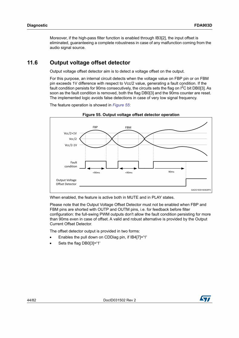
11.6 Output voltage offset detectorOutput voltage offset detector aim is to detect a voltage offset on the output.
For this purpose, an internal circuit detects when the voltage value on FBP pin or on FBM pin exceeds 1V difference with respect to Vcc/2 value, generating a fault condition. If the fault condition persists for 90ms consecutively, the circuits sets the flag on I2C bit DB0[3]. As soon as the fault condition is removed, both the flag DB0[3] and the 90ms counter are reset. The implemented logic avoids false detections in case of very low signal frequency.
The feature operation is showed in Figure 55:
Figure 55. Output voltage offset detector operation
When enabled, the feature is active both in MUTE and in PLAY states.
Please note that the Output Voltage Offset Detector must not be enabled when FBP and FBM pins are shorted with OUTP and OUTM pins, i.e. for feedback before filter configuration: the full-swing PWM outputs don't allow the fault condition persisting for more than 90ms even in case of offset. A valid and robust alternative is provided by the Output Current Offset Detector.
The offset detector output is provided in two forms: Enables the pull down on CDDiag pin, if IB4[7]='1' Sets the flag DB0[3]='1'

DocID031502 Rev 2 45/82
FDA903D Diagnostic
81
11.7 Output current offset detectorOutput current offset detector aim is to detect a current offset on the output.
11.7.1 Output current offset detector operation principleThe device senses the differential DC current flowing through the output pins OUTP and OUTM. In particular, in reference to Figure 56, the measured current offset is:
IOFFSET = |IOUTP-IOUTM|/2.
Figure 56. Current offset measurement
The measured current offset is then compared with a current threshold, which can be set by means of I2C bits IB10[4,3]: if it exceeds the chosen threshold, the device communicate that an output current offset has been detected.
11.7.2 Result communication and I2C controlThe output current offset detection consists in one single-shot test. The feature is controlled through I2C commands.
In order to start the detection, the user must set IB3[3]='1'.
At the end of the test, the internal control logic performs the following operations: Sets DB0[6]='1' to communicate that the test is ended and the result is valid Sets DB0[5]='1' if an offset has been detected, or DB0[5]='0' if no offset has been
detected Sets IB3[3]='0', allowing the user to perform another test afterwards
The detection can be start in MUTE state or in PLAY state. If the user sets IB3[3]='1' while the device FSM state is different, the test starts as soon as the device FSM enters in MUTE or PLAY state.
11.7.3 Hot spot detectionThe output current offset detector enables the possibility to detect a soft short to Vcc or to Gnd occurring when the PWM is already turned on, guaranteeing improved robustness against hot spot formation.
The operation principle is shown in Figure 57:

Diagnostic FDA903D
46/82 DocID031502 Rev 2
Figure 57. Hot spot detection
In standard operative condition, the DC value of IOUTP and IOUTM is zero, therefore the measured output current offset is zero.
When a soft short is connected between one output and Vcc or Gnd, the corresponding output drives an additional current ISHORT. The device interprets half of the mentioned current as offset: IOFFSET = |IOUTP-IOUTM|/2 = |ISHORT|/2.
In conclusion, if half of the DC current flowing in the short circuit exceeds the threshold selected through IB10[4,3], Output Current Offset Detector communicates an offset detection.
11.8 PWM pulse skipping detectorPulse skipping detector aim is to detect the PWM stage saturation.
The feature detects pulse skipping when, for each output, at least two consecutive PWM commutations have been skipped. The operation is shown in Figure 58:
Figure 58. PWM pulse skipping detector operation
In order to enable the PWM pulse skipping detector, the user must set IB5[5,4]='01'.
When detecting pulse skipping, the feature provides the output in two forms: Enables the pull down on CDDiag pin Sets the flag DB1[0]='1'
As soon as the pulse skipping condition is removed, both the outputs are reset.
The suggested utilization for this function is to connect a low-pass filter to CDDiag pin, therefore comparing the output with a voltage threshold. The lower is the CDDiag pin average voltage, the higher is the distortion.
DocID031502 Rev 2 47/82
FDA903D Diagnostic
81
11.9 Thermal protectionThe device integrates different protection levels against over-temperature conditions.
The first protection level consists only in communicating if the temperature exceeds four different thresholds, from TW4 to TW1. The result is provided in two ways: Setting DB1[7-4]; Pulling down the CDDiag pin, coherently with the setting of IB4[6-4].
If needed, the user is in charge of taking proper actions to counteract the temperature rising.
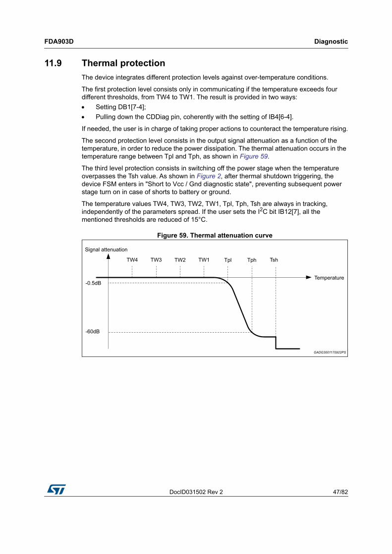
The second protection level consists in the output signal attenuation as a function of the temperature, in order to reduce the power dissipation. The thermal attenuation occurs in the temperature range between Tpl and Tph, as shown in Figure 59.
The third level protection consists in switching off the power stage when the temperature overpasses the Tsh value. As shown in Figure 2, after thermal shutdown triggering, the device FSM enters in "Short to Vcc / Gnd diagnostic state", preventing subsequent power stage turn on in case of shorts to battery or ground.
The temperature values TW4, TW3, TW2, TW1, Tpl, Tph, Tsh are always in tracking, independently of the parameters spread. If the user sets the I2C bit IB12[7], all the mentioned thresholds are reduced of 15°C.
Figure 59. Thermal attenuation curve

Diagnostic FDA903D
48/82 DocID031502 Rev 2
11.10 Watch-dogThe user can enable an internal watch-dog, setting I2C IB9[4]='1'.
The function is based on a timer which is reset at each Word Select line rising edge, and which reaches the timeout in: 2.9 ms if fs = 44.1 kHz; 2.7 ms if fs = 48 kHz, 96 kHz, 192 kHz.
When the timer reaches the timeout, the function performs two operations: Sends a muting command to the amplifier Sets a flag on DB6[2]
In case of timeout, the muting command is released as soon as the timer is reset by a new Word Select line edge.
11.11 Error frame checkThe device integrates a function called "Error frame check", which is permanently enabled.
The function counts the number of rising edges received on the Clock line, starting from each rising edge of Word Select line. At the end of the data frame, marked by the subsequent rising edge on Word Select line, the function checks that the reached count is coherent with the I2C configuration of the I2S protocol.
In case the function detects an error, the device sets a flag on DB6[1].
DocID031502 Rev 2 49/82
FDA903D Additional features
81
12 Additional features
12.1 AM operation modeThe device provides special functions in order to avoid EM interferences when the radio is tuned on an AM station.
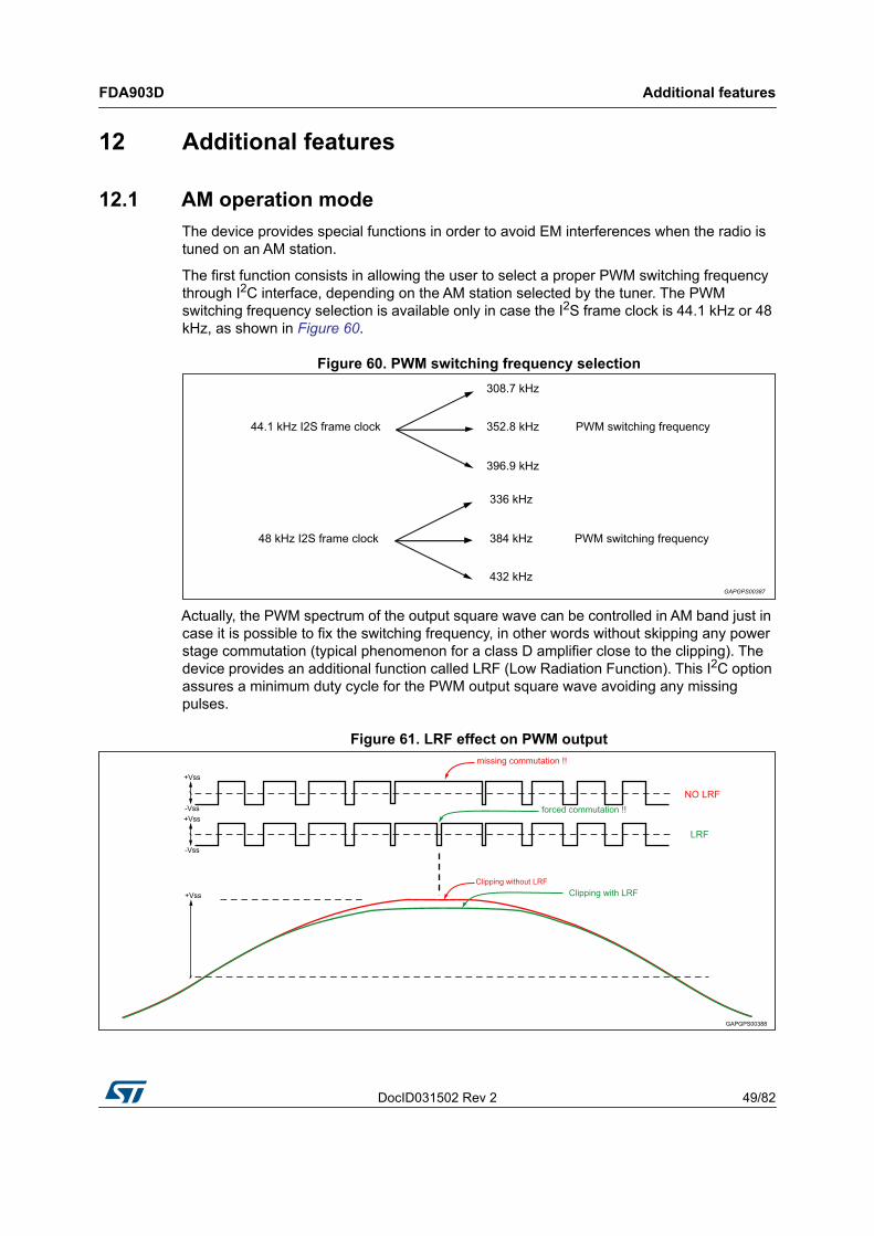
The first function consists in allowing the user to select a proper PWM switching frequency through I2C interface, depending on the AM station selected by the tuner. The PWM switching frequency selection is available only in case the I2S frame clock is 44.1 kHz or 48 kHz, as shown in Figure 60.
Figure 60. PWM switching frequency selection
Actually, the PWM spectrum of the output square wave can be controlled in AM band just in case it is possible to fix the switching frequency, in other words without skipping any power stage commutation (typical phenomenon for a class D amplifier close to the clipping). The device provides an additional function called LRF (Low Radiation Function). This I2C option assures a minimum duty cycle for the PWM output square wave avoiding any missing pulses.
Figure 61. LRF effect on PWM output

Additional features FDA903D
50/82 DocID031502 Rev 2
Please note that, by limiting the PWM duty cycle, a limitation of the output power occurs: the output power in case of usage of LRF function decreases about 10 % @ 1 % THD.
12.2 Noise gatingNoise gating is an automatic noise reduction feature that activates when output signal reaches not audible levels.
When input signal levels falls below -109 dBFs, the system activity is automatically optimized in order to exploit very low noise level on the output speakers.
The noise gating process has a 500 ms watching time before turning on, in order to avoid spurious activations.
The feature is enabled by default and can be disabled selecting IB3[1].
12.3 Dither PWMThe device implements a function, Dither PWM, which can be enabled through I2C bus by setting IB1[2].
The main target of this feature is to improve the EMC performances in the range [10 –30 MHz], especially in MUTE condition.
The function consists in modulating the period of the output PWM. The function doesn’t affect the average PWM frequency.
The modulation pattern is repeated every 8 PWM clock cycles, in order to avoid introducing significant noise in the audio bandwidth.
A qualitative example of the function operation is depicted in Figure 62.
Figure 62. Dither PWM effect on output PWM
Note: The use of this function is suggested only with In Phase modulation.

DocID031502 Rev 2 51/82
FDA903D Additional features
81
12.4 Real time load current monitoringFDA903D provides the current sensing function, an innovative feature for real time load monitoring. The continuous load monitoring enables many applications that could check, control and optimize the speakers operation for their entire life.
The current sensing circuit is the basis for the following diagnostic features: DC Diagnostic, Open Load in Play Detector and Output Current Offset Detector.
When the user enables the real time load current monitoring, the data collected by the current sensing circuit is also properly processed and directly provided to the user through I2S bus.
The overall current sensing path is shown in Figure 63:
Figure 63. Current sensing path
In particular, the output data represents the following current: ICS=(IOUTP-IOUTM)/2.
12.4.1 Result communication and I2C controlIn order to enable the real time load current monitoring, the user must set IB8[3-1]='011'.
The default current sensing full scale is 8 A, but it can be configured through IB8[7,6].
The current sensing stream is provided on I2Stest pin according to the following instructions: The data stream matches the same timings of I2S clock and I2S word select, according
to the configuration set trough IB0[5-1] and IB1[7-5]. The feature is available both in I2S and in TDM mode, guaranteeing the maximum flexibility.
The I2Stest pin data could be generated on the I2S clock rising or on falling edge. The selection is possible properly setting IB7[1], thus adapting to user system requirements.
Each word is composed of 15 significant bits, placed in the 15 MSB of the 32-bits word marked by I2S word select slot. The words are coded with two's complement notation.

Additional features FDA903D
52/82 DocID031502 Rev 2
The current sensing full scale set through IB8[7,6] corresponds to the following 15-bit digital word read on I2Stest:– 437.5 mFs if WS = 44.1 kHz or 48 kHz, IB1[4,3]='00'– 500 mFs if WS = 44.1 kHz or 48 kHz, IB1[4,3]='01'– 562.5 mFs If WS = 44.1 kHz or 48 kHz, IB1[4,3]='10'– 250 mFs if WS = 96 kHz– 125 mFs if WS = 192 kHz
The function provides the current information only in MUTE and PLAY states.
12.4.2 Current sensing limitationsThe maximum current sensing full scale is 8 A, even if the device can drive up to 11 A typically.
The default full scale is 8 A. The user can choose a lower full scale in order to increase the resolution. However, setting a lower full scale is not suggested when enabling the Open Load in Play Detector or Output Current Offset Detector.
As depicted in Figure 63, the current sensing provides the measured differential current flowing through OUTP and OUTM, which is different from the current flowing through the speaker due to the external filter capacitors. This mentioned contribution could be significant at high frequency. Moreover, the current sensing circuit comprehends a low-pass filter attenuating signals over 20 kHz frequency.

DocID031502 Rev 2 53/82
FDA903D I2S bus interface
81
13 I2S bus interface
The device receives the audio signal through I2S bus.
The I2S bus is composed of three lines: Clock line (I2Sclk pin); Word Select line (I2Sws pin); Serial Data line (I2Sdata pin).
The Word Select line frequency must be always equal to the audio sampling frequency fs. According to the I2C setting of IB1[7-5], the device supports the following standards for sampling frequency: 44.1 kHz; 48 kHz; 96 kHz; 192 kHz.
According to the I2C setting of IB0[6-5], the user can send the audio signal with the following data formats: I2S standard (max fs = 192 kHz); TDM - 4CHs (max fs = 192 kHz); TDM - 8CHs (max fs = 96 kHz); TDM - 16CHs (max fs = 48 kHz).
For all the mentioned data formats, the user must provide the data word following two's complement representation, starting from the MSB. The data word is composed of 32 bits: the device processes only the first 24 most significant bits, while it does not care the least significant 8 bits.
The internal PLL locks on the Clock line signal: when the I2S clock is missing or corrupted, the PLL consequently unlocks and the device forces the finite state machine in standby state. Furthermore, since the Clock line frequency is dependent on I2S bus configuration, it is strictly necessary to configure the I2C bits IB0[6-5] and IB1[7-5] accordingly.

I2S bus interface FDA903D
54/82 DocID031502 Rev 2
13.1 I2S standard mode descriptionThe I2S standard format is shown in Figure 64.
The Clock line frequency is equal to 64 fs.
With a proper I2C configuration, the user can select the channel containing the data to be processed: Right channel - IB0[4-1]='0000' Left channel - IB0[4-1]='0001'
Figure 64. I2S standard mode
13.2 TDM 4CH mode descriptionThe TDM4 format is shown in Figure 65.
The clock line frequency is equal to 128 fs.
With a proper I2C configuration, the user can select the slot containing the data to be processed: Slot 0 - IB0[4-1]='0000'’ Slot 1 - IB0[4-1]='0001'’ Slot 2 - IB0[4-1]='0010'’ Slot 3 - IB0[4-1]='0011'.
Figure 65. TDM4 mode
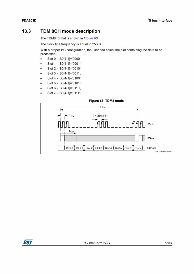
DocID031502 Rev 2 55/82
FDA903D I2S bus interface
81
13.3 TDM 8CH mode descriptionThe TDM8 format is shown in Figure 66.
The clock line frequency is equal to 256 fs.
With a proper I2C configuration, the user can select the slot containing the data to be processed: Slot 0 - IB0[4-1]='0000', Slot 1 - IB0[4-1]='0001', Slot 2 - IB0[4-1]='0010', Slot 3 - IB0[4-1]='0011', Slot 4 - IB0[4-1]='0100', Slot 5 - IB0[4-1]='0101', Slot 6 - IB0[4-1]='0110', Slot 7 - IB0[4-1]='0111'.
Figure 66. TDM8 mode
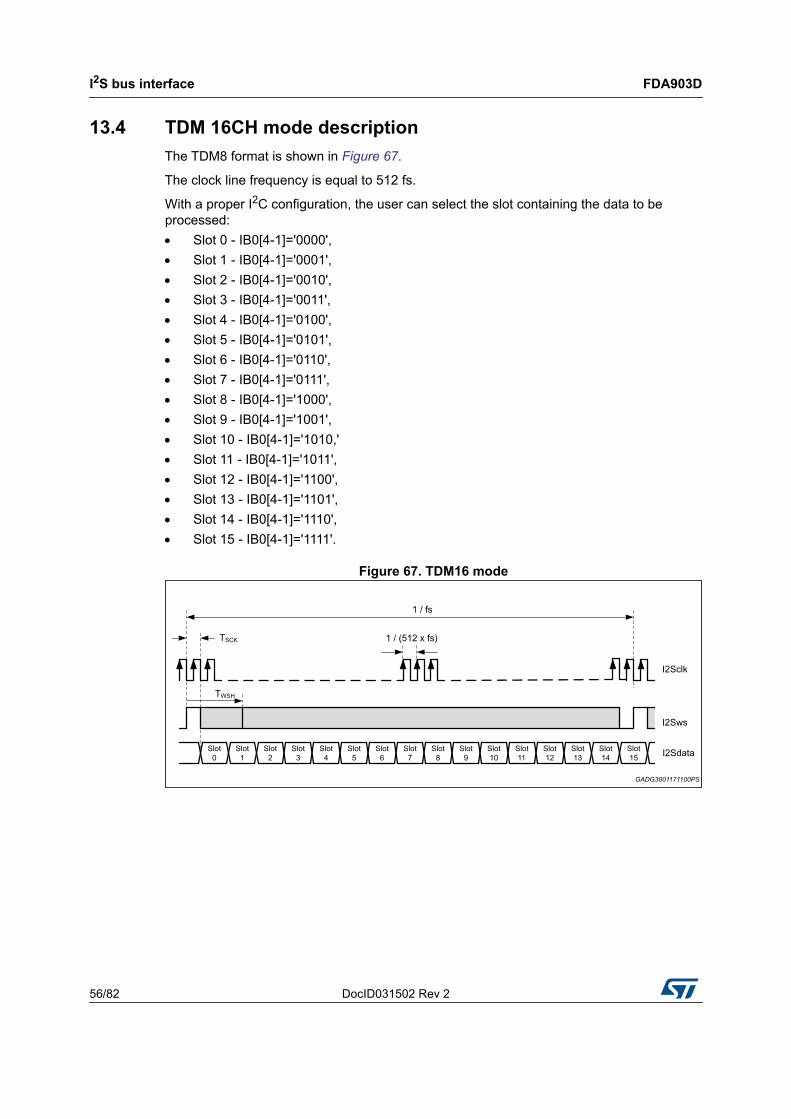
I2S bus interface FDA903D
56/82 DocID031502 Rev 2
13.4 TDM 16CH mode descriptionThe TDM8 format is shown in Figure 67.
The clock line frequency is equal to 512 fs.
With a proper I2C configuration, the user can select the slot containing the data to be processed: Slot 0 - IB0[4-1]='0000', Slot 1 - IB0[4-1]='0001', Slot 2 - IB0[4-1]='0010', Slot 3 - IB0[4-1]='0011', Slot 4 - IB0[4-1]='0100', Slot 5 - IB0[4-1]='0101', Slot 6 - IB0[4-1]='0110', Slot 7 - IB0[4-1]='0111', Slot 8 - IB0[4-1]='1000', Slot 9 - IB0[4-1]='1001', Slot 10 - IB0[4-1]='1010,' Slot 11 - IB0[4-1]='1011', Slot 12 - IB0[4-1]='1100', Slot 13 - IB0[4-1]='1101', Slot 14 - IB0[4-1]='1110', Slot 15 - IB0[4-1]='1111'.
Figure 67. TDM16 mode

DocID031502 Rev 2 57/82
FDA903D I2S bus interface
81
13.5 Timing requirements
Figure 68. I2S Interface timings
Figure 69. I2S clock transition timings
Table 10. I2S Interface timings Symbol Parameter Note Min Max Unit
TSCK
I2S clock period 40.69 ns
I2S clock period tolerance 0.9 x TSCK 1.1 x TSCK
I2S clock duty cycle 40 60 %
TSCKH I2S clock high time 15 ns
TSCKL I2S clock low time 15 ns
TSCKT I2S clock transition time 6 ns
TDS
I2S data (and word select) setup time (before I2S clock rising edge)
8 ns
TDH
I2S data (and word select) hold time (after I2S clock rising edge)
8 ns
TWSH I2S word select high time
I2S standard 32 x TSCK
TDM4 format 1 x TSCK 127 x TSCK
TDM8 format 1 x TSCK 255 x TSCK
TDM16 format 1 x TSCK 511 x TSCK
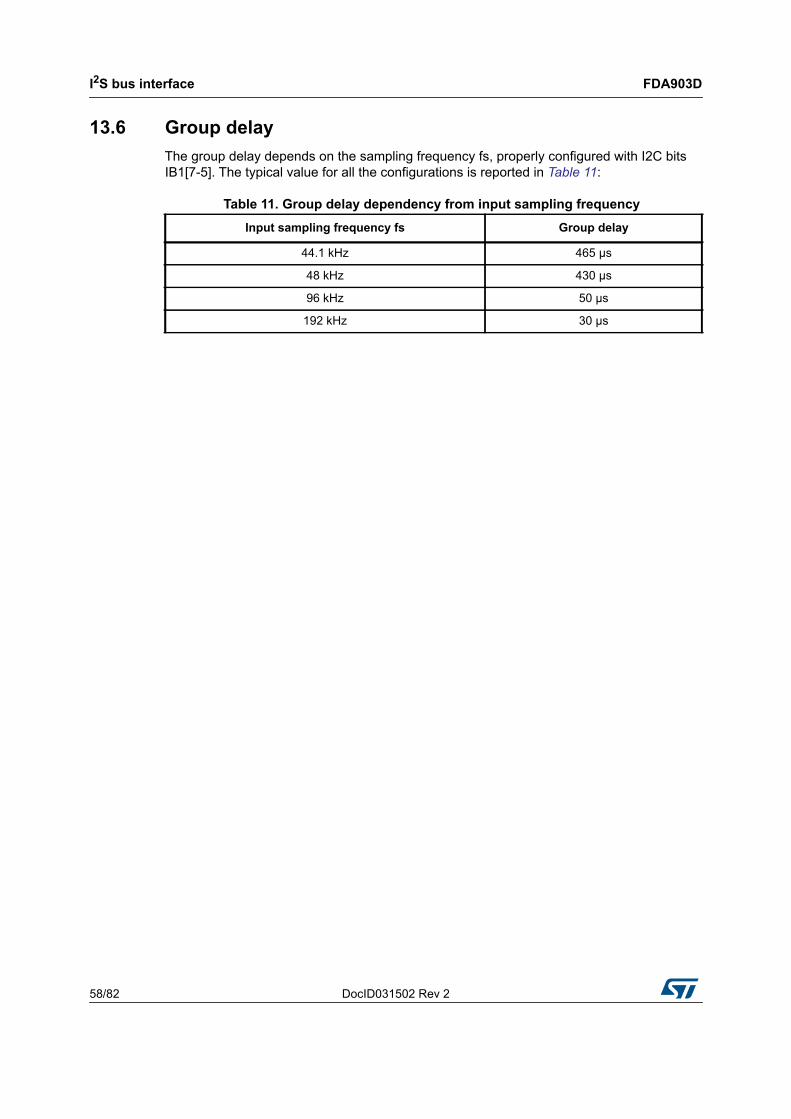
I2S bus interface FDA903D
58/82 DocID031502 Rev 2
13.6 Group delayThe group delay depends on the sampling frequency fs, properly configured with I2C bits IB1[7-5]. The typical value for all the configurations is reported in Table 11:
Table 11. Group delay dependency from input sampling frequency Input sampling frequency fs Group delay
44.1 kHz 465 μs
48 kHz 430 μs
96 kHz 50 μs
192 kHz 30 μs

DocID031502 Rev 2 59/82
FDA903D I2C bus interface
81
14 I2C bus interface
Data transmission from microprocessor to the FDA903D and viceversa takes place through the 2 wires I2C bus interface, consisting of the two lines SDA and SCL (pull-up resistors to positive supply voltage must be connected).
When I2C bus is active any operating mode of the IC may be modified and the diagnostic may be controlled and results read back.
The protocol used for the bus is depicted in Figure 70 and comprises: a start condition (S) a chip address byte (the LSB bit determines read/write transmission) a subaddress byte a sequence of data (N-bytes + acknowledge) a stop condition (P)
Figure 70. I2C bus protocol description
1. The I2C addresses are:Address 1 = 1110000Address 2 = 1110001Address 3 = 1110010Address 4 = 1110011Address 5 = 1110100Address 6 = 1110101Address 7 = 1110110Address 8 = 1110111
Description:– S = Start– R/W = '0' => Receive-Mode (Chip could be programmed by μP)– I = Auto increment; when 1, the address is automatically incremented for each
byte transferred– X: not used– A = Acknowledge– P = Stop– MAX CLOCK SPEED 400kbit/sec

I2C bus interface FDA903D
60/82 DocID031502 Rev 2
14.1 Writing procedureThere are two possible procedures:1. without increment: the I bit is set to 0 and the register is addressed by the subaddress.
Only this register is written by the data following the subaddress byte.2. with increment: the I bit is set to 1 and the first register write is the one addressed by
subaddress. The registers are written from this address up to stop bit or the reaching of last register.
14.2 Reading procedureThe reading procedure is made up only by the device address (sent by master) and the data (sent by slave) as reported in Figure 71 (a). In particular when a reading procedure is performed the first register read is the last addressed in a previous access to I2C peripheral.
Hence, to read a particular register also a sort of write action (a write interrupted after the sub-address is sent) is needed to specify which register has to be read. Figure 71 (b) shows the complete procedure to read a specific register where: the master performs a write action by sending just the device address and the
subaddress; the transmission must be interrupted with the stop condition when the subaddress is sent.
now, the read procedure can be performed: the master starts a new communication and sends the device address; then the slave (FDA903D) will respond by sending the data bits.
the read communication is ended by the master which sends a stop condition preceded by a not-acknowledge.
Instead, performing a start immediately after the stop condition could be possible for generating the repeated start condition (Sr) which also keeps busy the I2C bus until the stop is reached (Figure 71 (c)).
Figure 71. Reading procedure
There are two possible reading procedures:1. without auto-increment (Figure 72 (a)) if the "I" bit of the last I2C writing procedure has
been set to 0: in this case only the register addressed by the sub-address sent in the previous writing procedure is read;
2. with auto-increment (Figure 72 (b)) if the "I" bit of the last I2C write procedure has been set to 1: in this case the first register read is the one addressed by sub-address sent in the previous writing procedure. Only the registers from this address up to the stop bit are read.
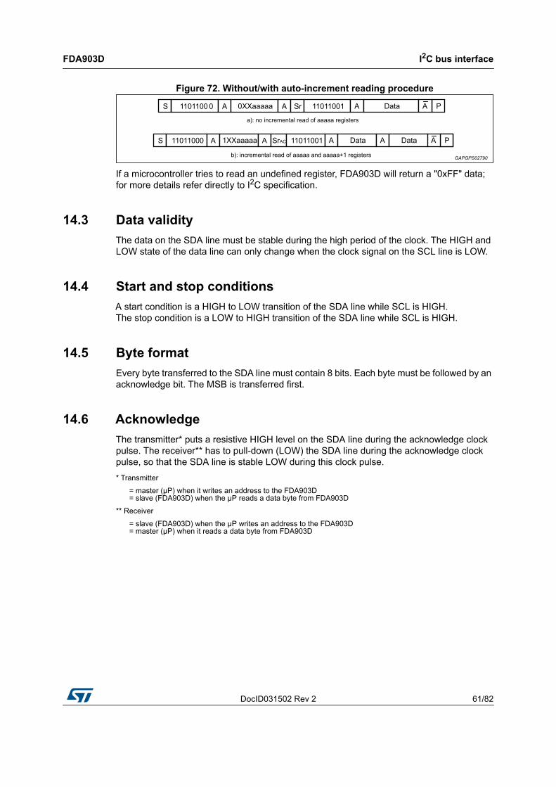
DocID031502 Rev 2 61/82
FDA903D I2C bus interface
81
Figure 72. Without/with auto-increment reading procedure
If a microcontroller tries to read an undefined register, FDA903D will return a "0xFF" data; for more details refer directly to I2C specification.
14.3 Data validityThe data on the SDA line must be stable during the high period of the clock. The HIGH and LOW state of the data line can only change when the clock signal on the SCL line is LOW.
14.4 Start and stop conditionsA start condition is a HIGH to LOW transition of the SDA line while SCL is HIGH. The stop condition is a LOW to HIGH transition of the SDA line while SCL is HIGH.
14.5 Byte formatEvery byte transferred to the SDA line must contain 8 bits. Each byte must be followed by an acknowledge bit. The MSB is transferred first.
14.6 AcknowledgeThe transmitter* puts a resistive HIGH level on the SDA line during the acknowledge clock pulse. The receiver** has to pull-down (LOW) the SDA line during the acknowledge clock pulse, so that the SDA line is stable LOW during this clock pulse.* Transmitter
= master (μP) when it writes an address to the FDA903D = slave (FDA903D) when the μP reads a data byte from FDA903D
** Receiver
= slave (FDA903D) when the μP writes an address to the FDA903D = master (μP) when it reads a data byte from FDA903D

I2C bus interface FDA903D
62/82 DocID031502 Rev 2
14.7 I2C timingThis paragraph describes more in detail the I2C bus protocol used and its timings.
Please refer to Table 12 and Figure 73 below.
Figure 73. I2C bus interface timing
Table 12. I2C bus interface timing
Symbol Parameter Min Max Unit
Fscl SCL (clock line) frequency - 400 kHzTscl SCL period 2500 - nsTsclh SCL high time 0.6 - μsTscll SCL low time 1.3 - μs
Tsstart Setup time for start condition 0.6 - μsThstart Hold time for start condition 0.6 - μsTsstop Setup time for stop condition 0.6 - μsTbuf Bus free time between a stop and a start condition 1.3 - μs
Tssda Setup time for data line 100 - nsThsda Hold time for data line 0(1)
1. Device must internally provide a hold time of at least 300 ns for the SDA signal to bridge the undefined region of the falling edge of SCL.
- nsTf Fall time for SCL and SDA - 300 ns
DocID031502 Rev 2 63/82
FDA903D I2C bus interface
81
14.8 I2S, I2C and Enable relationshipFDA903D provides both I2C and I2S communication by means of two different digital interfaces but connected to each other interfaces and clock domains.
To program the I2C interface the I2S clock must be present, and at least 10 ms should have passed from the Enable pins setting event.
In FDA903D the digital part has different clock domains: The I2C programming block clock is the I2C clock The I2S receiver clock which is the I2S clock The system clock which is generated by an internal PLL.
The I2C commands are not effective if I2S clock is not present. However they will remain memorized inside I2C registers.
If I2S clock is lost the digital machine goes in standby.
I2S clock (SCK) should be given to device before enabling it (Enable pins set to ‘out of standby’).

I2C register FDA903D
64/82 DocID031502 Rev 2
15 I2C register
15.1 Instruction bytes- “I00xxxxx”
Table 13. IB0-ADDR: “I0000000” Data bit Default value Definition
D7 0Lock bit:0 - Write on IBs is enable1 - Write on IBs is disable
D6
00
Digital input settings:
D5
D4-D1 0000
4 bits for channel position selection for I2S standard, TDM4, 8 and 16:D4-D1 Position selection0000 slot 0 (TDM mode) - right ch. (I2S mode0001 slot 1 (TDM mode) - left ch. (I2S mode)0010 slot 2 (TDM mode) 0011 slot 3 (TDM mode)0100 slot 4 (TDM 8 and 16 mode)0101 slot 5 (TDM 8 and 16 mode)0110 slot 6 (TDM 8 and 16 mode)0111 slot 7 (TDM 8 and 16 mode)1000 slot 8 (TDM 16 mode)1001 slot 9 (TDM 16 mode)1010 slot 10 (TDM 16 mode)1011 slot 11 (TDM 16 mode)1100 slot 12 (TDM 16 mode)1101 slot 13 (TDM 16 only)1110 slot 14 (TDM 16 only)1111 slot 15 (TDM 16 only)
D0 0 0 - Standard voltage mode1 - Low voltage mode
D6-D5 Input setting
00 I2S standard
01 TDM – 4 CHs
10 TDM – 8 CHs
11 TDM – 16 CHs

DocID031502 Rev 2 65/82
FDA903D I2C register
81
Table 14. IB1-ADDR: “I0000001” Data bit Default value Definition
D7 - D6 00
Digital input frame sync frequency (Fs):D7-D6 Frame sync (WS) frequency00 44.1 kHz01 48 kHz10 96 kHz11 192 kHz
D5 0 Reserved
D4 - D3 00
Switching frequency expressed in kHz.D4-D3 I2S frame sync frequencies (WS) [kHz]
44.1 48 96 192 00 308.7 336 384 38401 352.8 384 384 38410 396.9 432 384 38411 Reserved Reserved Reserved Reserved
D2 00 - PWM amplifier clock not dithered1 - PWM amplifier clock dithered
D1 0 Reserved
D0 00 - PWM in phase1 - PWM out of phase

I2C register FDA903D
66/82 DocID031502 Rev 2
Table 15. IB2-ADDR: “I0000010” Data bit Default value Definition
D7-D6 00
"DiagShort2Supply" timing selection:D7-D6 Timing00 90 ms01 70 ms10 45 ms11 20 ms
D5 0 Reserved
D4 00 - Low radiation function OFF1 - Low radiation function ON
D3 - D0 0000
Power limiting Function configurationD3-D0 Power limiting Config0000 Power limiter disabled0001 Power limited with maximum voltage scale at 15%0010 Power limited with maximum voltage scale at 20%0011 Power limited with maximum voltage scale at 25% 0100 Power limited with maximum voltage scale at 30%0101 Power limited with maximum voltage scale at 35%0110 Power limited with maximum voltage scale at 40%0111 Power limited with maximum voltage scale at 45%1000 Power limited with maximum voltage scale at 50%1001 Power limited with maximum voltage scale at 60%1010 Power limited with maximum voltage scale at 70%1011 Power limited with maximum voltage scale at 80%1100 Reserved1101 Reserved1110 Reserved1111 Reserved

DocID031502 Rev 2 67/82
FDA903D I2C register
81
Table 16. IB3-ADDR: “I0000011” Data bit Default value Definition
D7 - D7 0 Reserved
D5 0 0 - Output Voltage offset detector disable1 - Output Voltage offset detector enable
D4 0 0 - Input offset detector disable1 - Input offset detector enable
D3 0 0 - Output Current offset / hot spot detector disable1 - Output Current offset / hot spot detector enable
D2 0 0 - No Highpass in the DAC1 - Highpass in the DAC
D1 0 0 - Noise gating enable1 - Noise gating disable
D0 0 0 - Open Load detection in play disable1 - Open Load detection in play enable
Table 17. IB4-ADDR: “I0000100” - CDDiag pin configuration Data bit Default value Definition
D7 00 - No Output Voltage offset information on CDDiag pin1 - Output Voltage offset information on CDDiag pin
D6-D4 00
Temperature warning information on CD/DIAG pin:D6-D4 CDDiag configuration000 No thermal warning001 TW1010 TW2011 TW3100 TW4101 Reserved110 Reserved111 Reserved
D3 00 - No Overcurrent information on CD/DIAG pin1 - Overcurrent information on CD/DIAG pin
D2 00 - No Input Offset information on CD/DIAG pin1 - Input Offset information on CD/DIAG pin
D1 00 - No Short to Vcc / Short to GND information on CD/DIAG pin1 - Short to Vcc / Short to GND information on CD/DIAG pin
D0 00 - No High Voltage Mute information on CD/Diag pin1 - High Voltage Mute information on CD/Diag pin

I2C register FDA903D
68/82 DocID031502 Rev 2
Table 18. IB5-ADDR: “I0000101” - CDDiag pin configuration Data bit Default value Definition
D7 00 - No UVLOVCC information on CDDiag pin1 - UVLOVCC information on CDDiag pin
D6 00 - No Thermal shutdown information on CDDiag pin1 - Thermal shutdown information on CDDiag pin
D5-D4 00
Clipping information on CDDiag pin:D5-D4 CDDiag configuration00 No clipping information01 PWM Pulse Skipping detector10 Reserved11 Reserved
D3-D0 0000 Reserved
Table 19. IB6-ADDR: “I0000110” Data bit Default value Definition
D7-D6 00
Mute timing setup, (values with fsample = 44.1 kHz):D7-D6 Type of mute Mute time Unit00 Very Fast 3 ms01 Fast 45 ms10 Slow 90 ms11 Very Slow 185 ms
D5 0Audio signal gain control:0 - standard digital audio gain1 - +6 db digital audio gain
D4 00 - standard gain1 - low gain
D3-D0 0000 Reserved
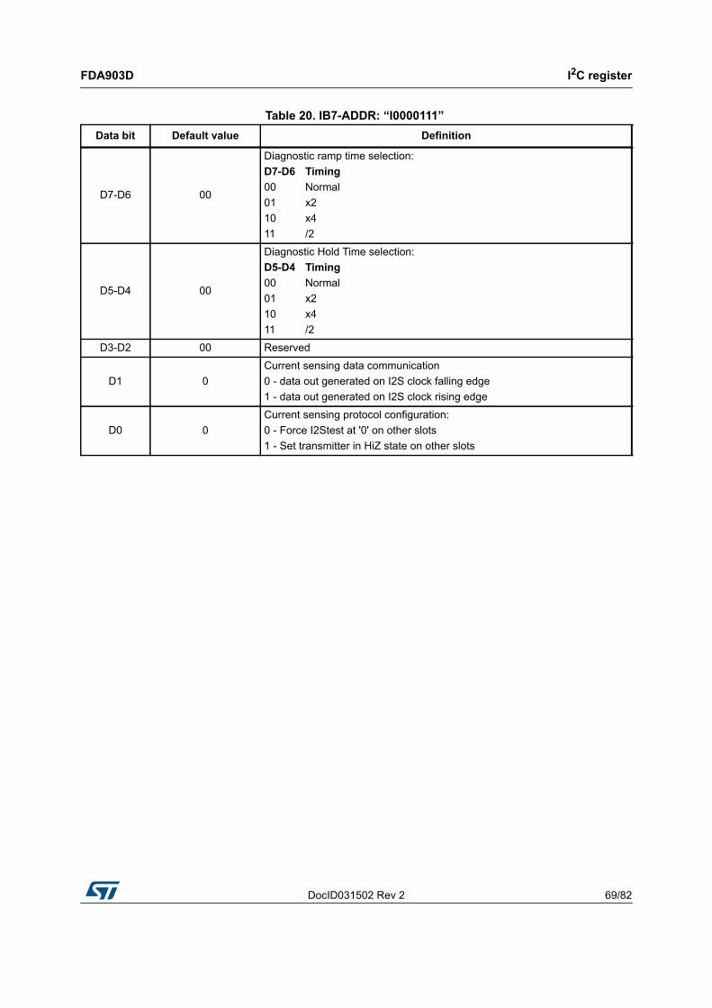
DocID031502 Rev 2 69/82
FDA903D I2C register
81
Table 20. IB7-ADDR: “I0000111” Data bit Default value Definition
D7-D6 00
Diagnostic ramp time selection:D7-D6 Timing00 Normal 01 x210 x411 /2
D5-D4 00
Diagnostic Hold Time selection:D5-D4 Timing00 Normal 01 x210 x411 /2
D3-D2 00 Reserved
D1 0Current sensing data communication 0 - data out generated on I2S clock falling edge 1 - data out generated on I2S clock rising edge
D0 0Current sensing protocol configuration: 0 - Force I2Stest at '0' on other slots 1 - Set transmitter in HiZ state on other slots

I2C register FDA903D
70/82 DocID031502 Rev 2
Table 21. IB8-ADDR: “I0001000” - CHANNEL CONTROLS Data bit Default value Definition
D7-D6 11
Current Sensing Full scale setting: D7-D6 Imax 00 1 A 01 2 A 10 4 A 11 8 A
D5 00 - Channel in TRISTATE (PWM OFF)1 - Channel with PWM ON
D4 00 - Channel DC Diag disable1 - Channel DC Diag start
D3-D1 000
I2Stest pin configuration:D3-D1 Function000 High impedance configuration001 Reserved010 Reserved011 Output: Current sensing enable100 Reserved101 Output: PWM synchronization signal110 Reserved111 Reserved
D0 00 - Channel in MUTE1 - Channel in PLAY
Table 22. IB9-ADDR: “I0001001” Data bit Default value Definition
D7-D5 000 Reserved
D4 00 - watch-dog for word select managing1 - no watch-dog for word select managing
D3-D0 0000 Reserved

DocID031502 Rev 2 71/82
FDA903D I2C register
81
Table 23. IB10-ADDR: “I0001010” Data bit Default value Definition
D7 0Short load impedance threshold (DC Diagnostic):0 - 0.75 Ω1 - 0.5 Ω
D6 0
Open load impedance threshold (DC Diagnostic & Open load in play detector):0 - 25 Ω1 - 15 Ω
D5 0 Reserved
D4-D3 10
Output Current Offset Detector threshold configurationD3-D2 Offset Detector threshold00 Reserved01 0.25 A (i.e. 2 V with 8 Ω load)10 0.5 A (i.e. 2 V with 4 Ω load)11 1.0 A (i.e. 2 V with 2 Ω load)
D2-D0 000 Reserved
Table 24. IB11-ADDR: “I0001011” Data bit Default value Definition
D7-D6 00 Reserved
D5-D4 0
Over current protection level selection: D5 D4 Iprot VDD>5.4VIprot VDD<5.4V0 0 11A 6A0 1 8A 6A1 0 6A 4A1 1 4A 4A
D3 00 - Deafult1 - PWM Slow Slope
D2-D0 000 Reserved
Table 25. IB12-ADDR: “I0001100” Data bit Default value Definition
D7 00 - Standard thermal warning1 - Thermal warning shift -15 °C
D6-D0 0001000 Reserved

I2C register FDA903D
72/82 DocID031502 Rev 2
Table 26. IB13-ADDR: “I0001101” Data bit Default value Definition
D7 0 Reserved
D6 0
0 - Digital mute enabled in PLAY when StartAnalogMute without Thermal Warning 1 occurs1 - Digital mute disabled in PLAY when StartAnalogMute without Thermal Warning 1 occurs
D5-D0 100000 Reserved
Table 27. IB14-ADDR: “I0001110”Data bit Default value Definition
D7-D5 000 Reserved
D4 00 - feedback on LC filter1 - feedback on Out Pin
D3
100
LC filter setup:
D2
D1
D0 00 – FIRST setup not programmed via I2C1 – FIRST setup programmed – ready to work
d3-d2-d1 LC filter000 Reserved001 10 μH + 2.2 μF Out Phase010 10 μH + 2.2 μF In Phase011 10 μH + 3.3 μF Out Phase100 10 μH + 3.3 μF In Phase101 10 μH + 4.7 μF Out Phase110 10 μH + 4.7 μF In Phase111 Reserved

DocID031502 Rev 2 73/82
FDA903D I2C register
81
15.2 Data bytes - “I01xxxxx”Legend:
Type "S/C": the hardware can only set the flag. An I2C reading operation clears the flag.
Type "SR/C": the hardware can set or reset the flag. An I2C reading operation clears the flag.
Type "SR": the hardware can both set or reset the flag. An I2C reading operation doesn't affect the flag.
Table 28. DB0-ADDR: “I0100000” Data bit Type Definition
D7 S/C0 – Offset at input not present1 – Offset at input present
D6 SR/C0 – Output Current offset not valid1 – Output Current offset valid
D5 SR/C0 – Output Current offset not present1 – Output Current offset present
D4 S/C Reserved
D3 S/C0 – Output Voltage offset not present1 – Output Voltage offset present
D2 SR/C 0 – Open Load in Play test not ended 1 – Open Load in Play test ended
D1 SR/C0 – Open Load in Play test input signal not valid1 – Open Load in Play test input signal valid
D0 SR/C0 – Open Load in Play not detected1 – Open Load in Play detected

I2C register FDA903D
74/82 DocID031502 Rev 2
Table 29. DB1-ADDR: “I0100001” Data bit Type Definition
D7 SR/C0 – Thermal warning 1 not active1 – Thermal warning 1 active
D6 SR/C0 – Thermal warning 2 not active1 – Thermal warning 2 active
D5 SR/C0 – Thermal warning 3 not active1 – Thermal warning 3 active
D4 SR/C0 – Thermal warning 4 not active1 – Thermal warning 4 active
D3 SR/C0 - PLL not locked1 - PLL locked
D2 S/C0 - UVLOALL not detected1 - UVLOALL detected(NOTE: after turn-on, the first reading of this flag will be always 1)
D1 S/C0 - No Overvoltage Shutdown detected1 - Overvoltage Shutdown detected
D0 S/C0 - PWM pulse skipping not detected1 - PWM pulse skipping detected
Table 30. DB2-ADDR:"I0100010" Data bit Type Definition
D7 SR/C0 – Channel DC diagnostic pulse not ended1 – Channel DC diagnostic pulse ended
D6 SR/C0 – Channel DC diagnostic data not valid1 – Channel DC diagnostic data valid
D5 S/C0 – Channel Over current not detected1 – Channel Over current protection triggered
D4 SR/C0 – No Short Load on Channel1 – Short Load on Channel
D3 SR0 – No Short to Vcc on Channel1 – Short to Vcc on Channel
D2 SR0 – No short to Gnd on Channel1 – Short to Gnd on Channel
D1 SR/C0 – No Open Load on Channel1 – Open Load on Channel
D0 SR/C0 – Channel in mute1 – Channel in play

DocID031502 Rev 2 75/82
FDA903D I2C register
81
Table 31. DB3-ADDR: “I0100011” DC Diagnostic Error code Data bit Type Definition
D7
SR/C DC Diagnostic Error code
D6
D5
D4
D3
D2
D1
D0
Table 32. DB4-ADDR:"I0100100" - Current Sensing data (10-8) Data bit Type Definition
D7-D3 SR Reserved
D2
SR Channel Current Sensing (10-8)D1
D0
Table 33. DB5-ADDR:"I0100101" - Current Sensing data (7-0) Data bit Type Definition
D7
SR Channel Current Sensing (7-0)
D6
D5
D4
D3
D2
D1
D0
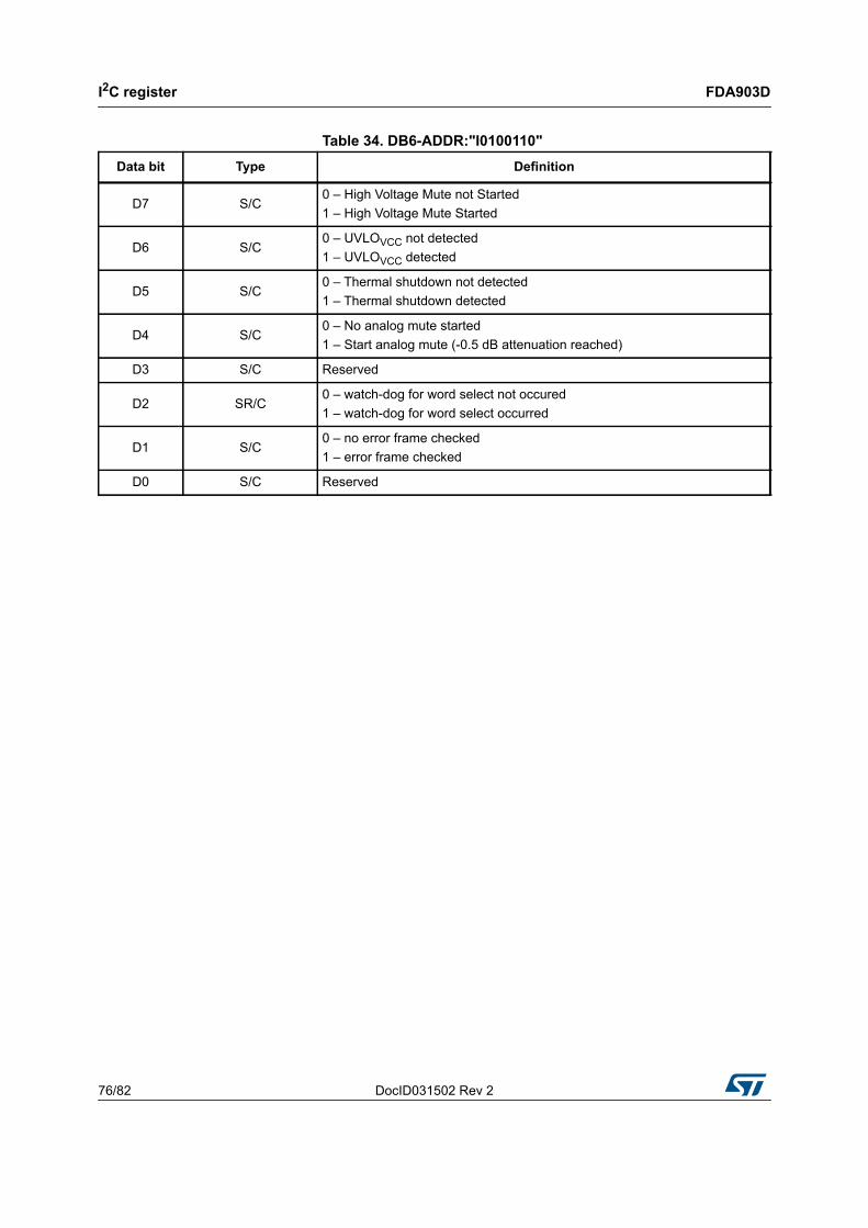
I2C register FDA903D
76/82 DocID031502 Rev 2
Table 34. DB6-ADDR:"I0100110" Data bit Type Definition
D7 S/C0 – High Voltage Mute not Started 1 – High Voltage Mute Started
D6 S/C0 – UVLOVCC not detected1 – UVLOVCC detected
D5 S/C0 – Thermal shutdown not detected1 – Thermal shutdown detected
D4 S/C0 – No analog mute started1 – Start analog mute (-0.5 dB attenuation reached)
D3 S/C Reserved
D2 SR/C0 – watch-dog for word select not occured1 – watch-dog for word select occurred
D1 S/C0 – no error frame checked1 – error frame checked
D0 S/C Reserved

DocID031502 Rev 2 77/82
FDA903D Package information
81
16 Package information
In order to meet environmental requirements, ST offers these devices in different grades of ECOPACK® packages, depending on their level of environmental compliance. ECOPACK® specifications, grade definitions and product status are available at: www.st.com. ECOPACK® is an ST trademark.
16.1 PowerSSO-36 (exposed pad) package information
Figure 74. PowerSSO-36 (exposed pad) package outline
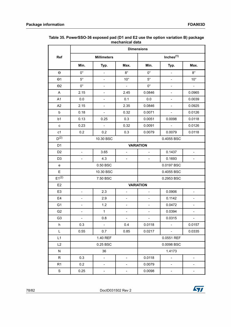
Package information FDA903D
78/82 DocID031502 Rev 2
Table 35. PowerSSO-36 exposed pad (D1 and E2 use the option variation B) package mechanical data
Ref
Dimensions
Millimeters Inches(1)
Min. Typ. Max. Min. Typ. Max.
Ө 0° - 8° 0° - 8°
Ө1 5° - 10° 5° - 10°
Ө2 0° - - 0° - -
A 2.15 - 2.45 0.0846 - 0.0965
A1 0.0 - 0.1 0.0 - 0.0039
A2 2.15 - 2.35 0.0846 - 0.0925
b 0.18 - 0.32 0.0071 - 0.0126
b1 0.13 0.25 0.3 0.0051 0.0098 0.0118
c 0.23 - 0.32 0.0091 - 0.0126
c1 0.2 0.2 0.3 0.0079 0.0079 0.0118
D(2) 10.30 BSC 0.4055 BSC
D1 VARIATION
D2 - 3.65 - - 0.1437 -
D3 - 4.3 - - 0.1693 -
e 0.50 BSC 0.0197 BSC
E 10.30 BSC 0.4055 BSC
E1(2) 7.50 BSC 0.2953 BSC
E2 VARIATION
E3 - 2.3 - - 0.0906 -
E4 - 2.9 - - 0.1142 -
G1 - 1.2 - - 0.0472 -
G2 - 1 - - 0.0394 -
G3 - 0.8 - - 0.0315 -
h 0.3 - 0.4 0.0118 - 0.0157
L 0.55 0.7 0.85 0.0217 - 0.0335
L1 1.40 REF 0.0551 REF
L2 0.25 BSC 0.0098 BSC
N 36 1.4173
R 0.3 - - 0.0118 - -
R1 0.2 - - 0.0079 - -
S 0.25 - - 0.0098 - -

DocID031502 Rev 2 79/82
FDA903D Package information
81
Tolerance of form and position
aaa 0.2 0.0079
bbb 0.2 0.0079
ccc 0.1 0.0039
ddd 0.2 0.0079
eee 0.1 0.0039
ffff 0.2 0.0079
ggg 0.15 0.0059
VARIATIONS
Option A
D1 6.5 - 7.1 0.2559 - 0.2795
E2 4.1 - 4.7 0.1614 - 0.1850
Option B
D1 4.9 - 5.5 0.1929 - 0.2165
E2 4.1 - 4.7 0.1614 - 0.1850
Option C
D1 6.9 - 7.5 0.2717 - 0.2953
E2 4.3 - 5.2 0.1693 - 0.2047
1. Values in inches are converted from mm and rounded to 4 decimal digits.
2. Dimensions D and E1 do not include mold flash or protrusions. Allowable mold flash or protrusions is ‘0.25 mm’ per side D and ‘0.15 mm’ per side E1. D and E1 are Maximum plastic body size dimensions including mold mismatch.
Table 35. PowerSSO-36 exposed pad (D1 and E2 use the option variation B) package mechanical data (continued)
Ref
Dimensions
Millimeters Inches(1)
Min. Typ. Max. Min. Typ. Max.

Package information FDA903D
80/82 DocID031502 Rev 2
16.2 Package marking information
Figure 75. PowerSSO-36 (exp. pad) marking information
Note: Engineering Samples: these samples are clearly identified by last two digits ‘ES’ in the marking of each unit. These samples are intended to be used for electrical compatibility evaluation only; usage for any other purpose may be agreed only upon written authorization by ST. ST is not liable for any customer usage in production and/or in reliability qualification trials.Commercial Samples: Fully qualified parts from ST standard production with no usage restrictions.

DocID031502 Rev 2 81/82
FDA903D Revision history
81
17 Revision history
Table 36. Document revision historyDate Revision Changes
26-Feb-2018 1 Initial release.
03-May-2018 2 Datasheet changed from Confidentiality level to Public.

FDA903D
82/82 DocID031502 Rev 2
IMPORTANT NOTICE – PLEASE READ CAREFULLY
STMicroelectronics NV and its subsidiaries (“ST”) reserve the right to make changes, corrections, enhancements, modifications, and improvements to ST products and/or to this document at any time without notice. Purchasers should obtain the latest relevant information on ST products before placing orders. ST products are sold pursuant to ST’s terms and conditions of sale in place at the time of order acknowledgement.
Purchasers are solely responsible for the choice, selection, and use of ST products and ST assumes no liability for application assistance or the design of Purchasers’ products.
No license, express or implied, to any intellectual property right is granted by ST herein.
Resale of ST products with provisions different from the information set forth herein shall void any warranty granted by ST for such product.
ST and the ST logo are trademarks of ST. All other product or service names are the property of their respective owners.
Information in this document supersedes and replaces information previously supplied in any prior versions of this document.
© 2018 STMicroelectronics – All rights reserved