Embed Size (px)
Citation preview
SCLS534C − AUGUST 2003 − REVISED APRIL 2008
1POST OFFICE BOX 655303 • DALLAS, TEXAS 75265
Qualified for Automotive Applications
ESD Protection Exceeds 2000 V PerMIL-STD-883, Method 3015; Exceeds 200 VUsing Machine Model (C = 200 pF, R = 0)
2-V to 5.5-V VCC Operation
Typical V OLP (Output Ground Bounce)<0.8 V at VCC = 3.3 V, TA = 25°C
Typical V OHV (Output V OH Undershoot)>2.3 V at VCC = 3.3 V, TA = 25°C
Support Mixed-Mode Voltage Operation onAll Ports
description/ordering information
The SN74LV86A is a quadruple 2-input exclusive-OR gate designed for 2-V to 5.5-V VCC operation.
This device contains four independent 2-input exclusive-OR gates. It performs the Boolean functionY = A B or Y = AB + AB in positive logic.
A common application is as a true/complement element. If one of the inputs is low, the other input is reproducedin true form at the output. If one of the inputs is high, the signal on the other input is reproduced inverted at theoutput.
ORDERING INFORMATION
TA PACKAGE ‡ ORDERABLEPART NUMBER
TOP-SIDEMARKING
−40°C to 105°C TSSOP − PW Tape and reel SN74LV86ATPWRQ1 LV86AT
† For the most current package and ordering information, see the Package Option Addendum at the endof this document, or see the TI web site at http://www.ti.com.
‡ Package drawings, thermal data, and symbolization are available at http://www.ti.com/packaging.
FUNCTION TABLE(each gate)
INPUTS OUTPUTA B
OUTPUTY
L L L
L H H
H L H
H H L
1
2
3
4
5
6
7
14
13
12
11
10
9
8
1A1B1Y2A2B2Y
GND
VCC4B4A4Y3B3A3Y
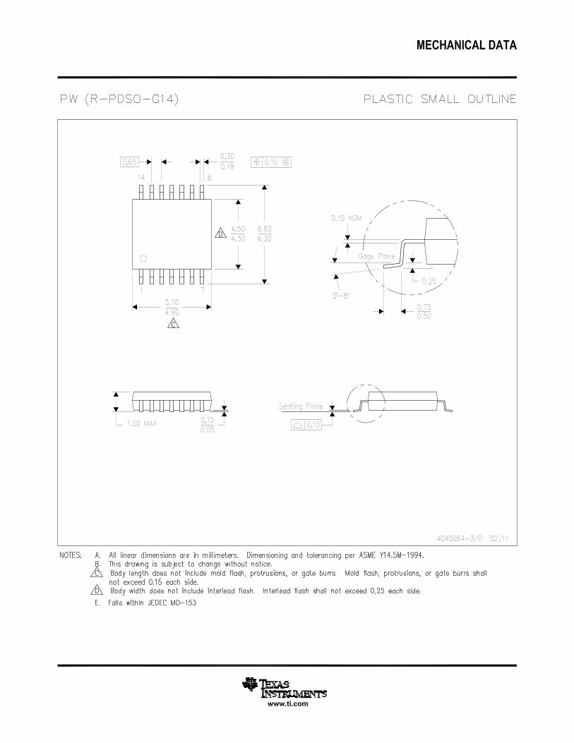
PW PACKAGE(TOP VIEW)
! " #$%! " &$'(#! )!%*)$#!" # ! "&%##!" &% !+% !%" %," "!$%!""!)) -!.* )$#! &#%""/ )%" ! %#%""(. #($)%!%"!/ (( &%!%"*
Copyright 2008, Texas Instruments Incorporated
Please be aware that an important notice concerning availability, standard warranty, and use in critical applications ofTexas Instruments semiconductor products and disclaimers thereto appears at the end of this data sheet.
SCLS534C − AUGUST 2003 − REVISED APRIL 2008
2 POST OFFICE BOX 655303 • DALLAS, TEXAS 75265
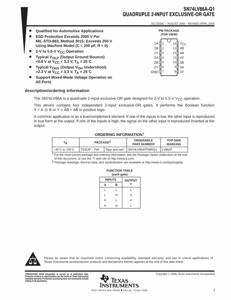
logic symbol †
11A
21B
1Y3
42A
52B
2Y6
93A
103B
3Y8
124A
134B
4Y11
=1
† This symbol is in accordance with ANSI/IEEE Std 91-1984 and IEC Publication 617-12.
exclusive-OR logic
An exclusive-OR gate has many applications, some of which can be represented better by alternative logicsymbols.
= 1
Exclusive OR
These are five equivalent exclusive-OR symbols valid for an ’LV86A gate in positive logic; negation can beshown at any two ports.
= 2k 2k + 1
Logic-Identity Element Even-Parity Element Odd-Parity Element
The output is active (low) ifall inputs stand at the samelogic level (i.e., A = B).
The output is active (low) ifan even number of inputs(i.e., 0 or 2) are active.
The output is active (high) ifan odd number of inputs (i.e.,only 1 of the 2) are active.
absolute maximum ratings over operating free-air temperature range (unless otherwise noted) ‡
Supply voltage range, VCC −0.5 V to 7 V. . . . . . . . . . . . . . . . . . . . . . . . . . . . . . . . . . . . . . . . . . . . . . . . . . . . . . . . . . Input voltage range, VI (see Note 1) −0.5 V to 7 V. . . . . . . . . . . . . . . . . . . . . . . . . . . . . . . . . . . . . . . . . . . . . . . . . . Voltage range applied to any output in the high-impedance
or power-off state, VO (see Note 1) −0.5 V to 7 V. . . . . . . . . . . . . . . . . . . . . . . . . . . . . . . . . . . . . . . . . . . . . . . . Output voltage range, VO (see Notes 1 and 2) −0.5 V to VCC + 0.5 V. . . . . . . . . . . . . . . . . . . . . . . . . . . . . . . . . . Input clamp current, IIK (VI < 0) −20 mA. . . . . . . . . . . . . . . . . . . . . . . . . . . . . . . . . . . . . . . . . . . . . . . . . . . . . . . . . . . Output clamp current, IOK (VO < 0) −50 mA. . . . . . . . . . . . . . . . . . . . . . . . . . . . . . . . . . . . . . . . . . . . . . . . . . . . . . . . Continuous output current, IO (VO = 0 to VCC) ±25 mA. . . . . . . . . . . . . . . . . . . . . . . . . . . . . . . . . . . . . . . . . . . . . . Continuous current through VCC or GND ±50 mA. . . . . . . . . . . . . . . . . . . . . . . . . . . . . . . . . . . . . . . . . . . . . . . . . . . Package thermal impedance, θJA (see Note 3) 113°C/W. . . . . . . . . . . . . . . . . . . . . . . . . . . . . . . . . . . . . . . . . . . . Storage temperature range, Tstg −65°C to 150°C. . . . . . . . . . . . . . . . . . . . . . . . . . . . . . . . . . . . . . . . . . . . . . . . . . .
‡ Stresses beyond those listed under “absolute maximum ratings” may cause permanent damage to the device. These are stress ratings only, andfunctional operation of the device at these or any other conditions beyond those indicated under “recommended operating conditions” is notimplied. Exposure to absolute-maximum-rated conditions for extended periods may affect device reliability.
NOTES: 1. The input and output negative-voltage ratings may be exceeded if the input and output current ratings are observed.2. This value is limited to 5.5 V maximum.3. The package thermal impedance is calculated in accordance with JESD 51-7.
SCLS534C − AUGUST 2003 − REVISED APRIL 2008
3POST OFFICE BOX 655303 • DALLAS, TEXAS 75265
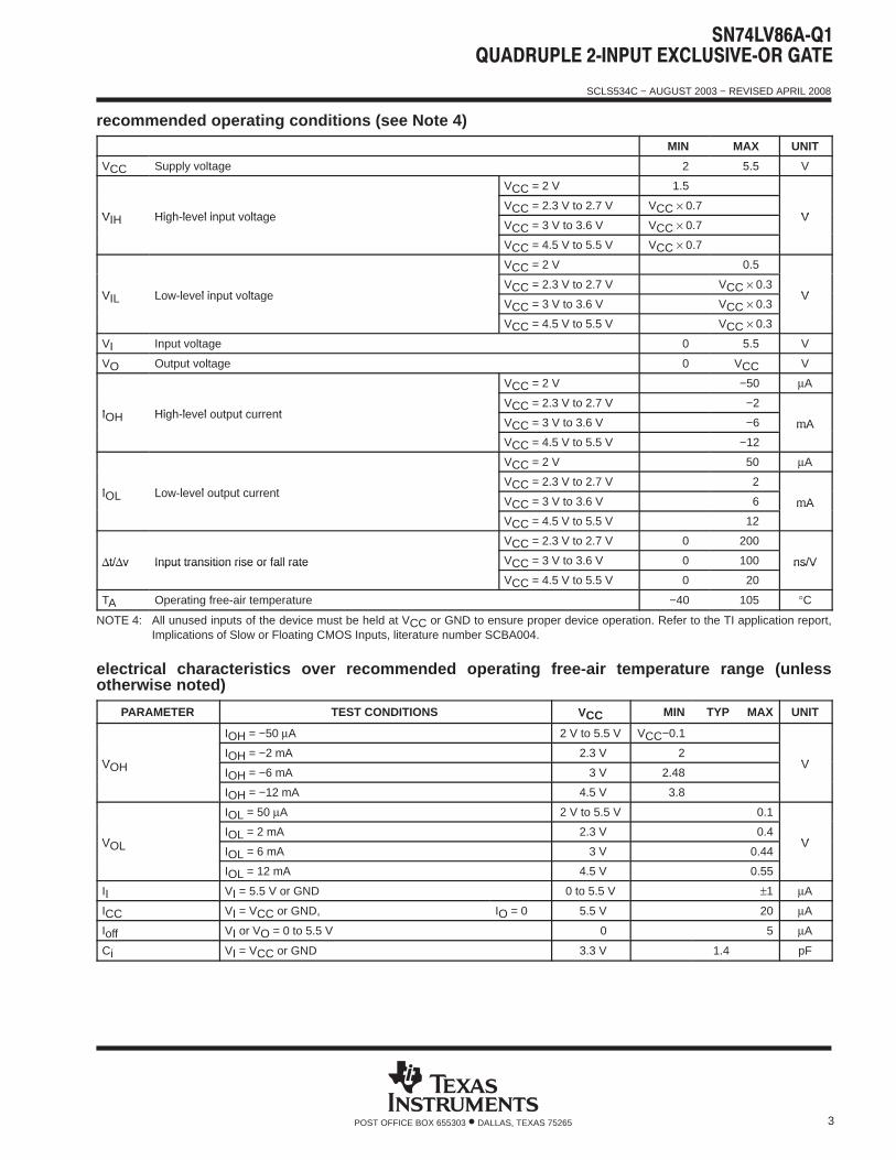
recommended operating conditions (see Note 4)
MIN MAX UNIT
VCC Supply voltage 2 5.5 V
VCC = 2 V 1.5
VIH High-level input voltageVCC = 2.3 V to 2.7 V VCC × 0.7
VVIH High-level input voltageVCC = 3 V to 3.6 V VCC × 0.7
V
VCC = 4.5 V to 5.5 V VCC × 0.7
VCC = 2 V 0.5
VIL Low-level input voltageVCC = 2.3 V to 2.7 V VCC × 0.3
VVIL Low-level input voltageVCC = 3 V to 3.6 V VCC × 0.3
V
VCC = 4.5 V to 5.5 V VCC × 0.3
VI Input voltage 0 5.5 V
VO Output voltage 0 VCC V
VCC = 2 V −50 µA
IOH High-level output currentVCC = 2.3 V to 2.7 V −2
IOH High-level output currentVCC = 3 V to 3.6 V −6 mA
VCC = 4.5 V to 5.5 V −12
mA
VCC = 2 V 50 µA
IOL Low-level output currentVCC = 2.3 V to 2.7 V 2
IOL Low-level output currentVCC = 3 V to 3.6 V 6 mA
VCC = 4.5 V to 5.5 V 12
mA
VCC = 2.3 V to 2.7 V 0 200
∆t/∆v Input transition rise or fall rate VCC = 3 V to 3.6 V 0 100 ns/V∆t/∆v Input transition rise or fall rate
VCC = 4.5 V to 5.5 V 0 20
ns/V
TA Operating free-air temperature −40 105 °C
NOTE 4: All unused inputs of the device must be held at VCC or GND to ensure proper device operation. Refer to the TI application report,Implications of Slow or Floating CMOS Inputs, literature number SCBA004.
electrical characteristics over recommended operating free-air temperature range (unlessotherwise noted)
PARAMETER TEST CONDITIONS VCC MIN TYP MAX UNIT
IOH = −50 µA 2 V to 5.5 V VCC−0.1
VOHIOH = −2 mA 2.3 V 2
VVOH IOH = −6 mA 3 V 2.48V
IOH = −12 mA 4.5 V 3.8
IOL = 50 µA 2 V to 5.5 V 0.1
VOLIOL = 2 mA 2.3 V 0.4
VVOL IOL = 6 mA 3 V 0.44V
IOL = 12 mA 4.5 V 0.55
II VI = 5.5 V or GND 0 to 5.5 V ±1 µA
ICC VI = VCC or GND, IO = 0 5.5 V 20 µA
Ioff VI or VO = 0 to 5.5 V 0 5 µA
Ci VI = VCC or GND 3.3 V 1.4 pF
SCLS534C − AUGUST 2003 − REVISED APRIL 2008
4 POST OFFICE BOX 655303 • DALLAS, TEXAS 75265
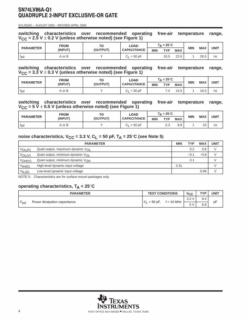
switching characteristics over recommended operating free-air temperature range,VCC = 2.5 V ± 0.2 V (unless otherwise noted) (see Figure 1)
PARAMETERFROM TO LOAD TA = 25°C
MIN MAX UNITPARAMETERFROM
(INPUT)TO
(OUTPUT)LOAD
CAPACITANCE MIN TYP MAXMIN MAX UNIT
tpd A or B Y CL = 50 pF 10.5 22.6 1 26.5 ns
switching characteristics over recommended operating free-air temperature range,VCC = 3.3 V ± 0.3 V (unless otherwise noted) (see Figure 1)
PARAMETERFROM TO LOAD TA = 25°C
MIN MAX UNITPARAMETERFROM
(INPUT)TO
(OUTPUT)LOAD
CAPACITANCE MIN TYP MAXMIN MAX UNIT
tpd A or B Y CL = 50 pF 7.4 14.5 1 16.5 ns
switching characteristics over recommended operating free-air temperature range,VCC = 5 V ± 0.5 V (unless otherwise noted) (see Figure 1)
PARAMETERFROM TO LOAD TA = 25°C
MIN MAX UNITPARAMETERFROM
(INPUT)TO
(OUTPUT)LOAD
CAPACITANCE MIN TYP MAXMIN MAX UNIT
tpd A or B Y CL = 50 pF 5.3 8.8 1 10 ns
noise characteristics, V CC = 3.3 V, CL = 50 pF, TA = 25°C (see Note 5 )
PARAMETER MIN TYP MAX UNIT
VOL(P) Quiet output, maximum dynamic VOL 0.2 0.8 V
VOL(V) Quiet output, minimum dynamic VOL −0.1 −0.8 V
VOH(V) Quiet output, minimum dynamic VOH 3.1 V
VIH(D) High-level dynamic input voltage 2.31 V
VIL(D) Low-level dynamic input voltage 0.99 V
NOTE 5: Characteristics are for surface-mount packages only.
operating characteristics, T A = 25°CPARAMETER TEST CONDITIONS VCC TYP UNIT
Cpd Power dissipation capacitance CL = 50 pF, f = 10 MHz3.3 V 8.4
pFCpd Power dissipation capacitance CL = 50 pF, f = 10 MHz5 V 8.8
pF
SCLS534C − AUGUST 2003 − REVISED APRIL 2008
5POST OFFICE BOX 655303 • DALLAS, TEXAS 75265
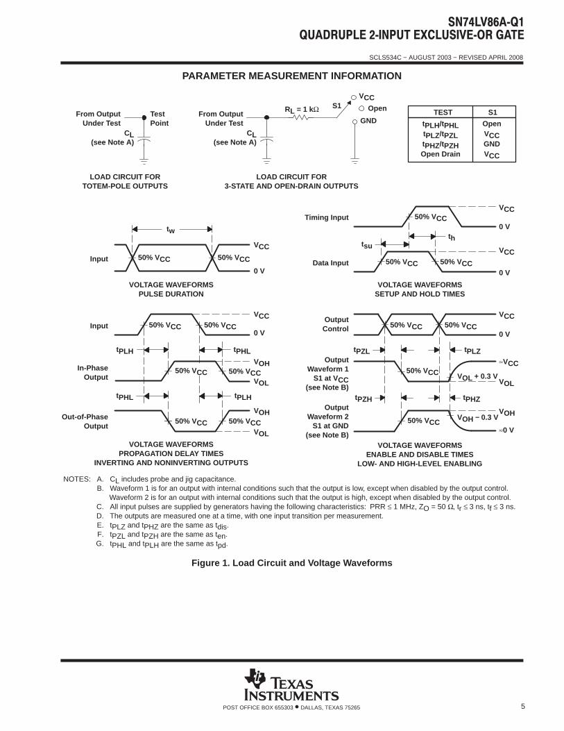
PARAMETER MEASUREMENT INFORMATION
50% VCC
VCC
VCC
0 V
0 V
thtsu
VOLTAGE WAVEFORMSSETUP AND HOLD TIMES
Data Input
tPLH
tPHL
tPHL
tPLH
VOH
VOH
VOL
VOL
VCC
0 V
50% VCC50% VCC
Input
Out-of-PhaseOutput
In-PhaseOutput
Timing Input
50% VCC
VOLTAGE WAVEFORMSPROPAGATION DELAY TIMES
INVERTING AND NONINVERTING OUTPUTS
OutputControl
OutputWaveform 1
S1 at VCC(see Note B)
OutputWaveform 2
S1 at GND(see Note B)
VOL
VOH
tPZL
tPZH
tPLZ
tPHZ
≈VCC
0 V
50% VCC VOL + 0.3 V
50% VCC≈0 V
VCC
VOLTAGE WAVEFORMSENABLE AND DISABLE TIMES
LOW- AND HIGH-LEVEL ENABLING
tPLH/tPHLtPLZ/tPZLtPHZ/tPZHOpen Drain
OpenVCCGNDVCC
TEST S1
VCC
0 V
50% VCC
tw
VOLTAGE WAVEFORMSPULSE DURATION
Input
NOTES: A. CL includes probe and jig capacitance.B. Waveform 1 is for an output with internal conditions such that the output is low, except when disabled by the output control.
Waveform 2 is for an output with internal conditions such that the output is high, except when disabled by the output control.C. All input pulses are supplied by generators having the following characteristics: PRR ≤ 1 MHz, ZO = 50 Ω, tr ≤ 3 ns, tf ≤ 3 ns.D. The outputs are measured one at a time, with one input transition per measurement.E. tPLZ and tPHZ are the same as tdis.F. tPZL and tPZH are the same as ten.G. tPHL and tPLH are the same as tpd.
From OutputUnder Test
CL(see Note A)
LOAD CIRCUIT FOR3-STATE AND OPEN-DRAIN OUTPUTS
S1VCC
RL = 1 kΩGND
From OutputUnder Test
CL(see Note A)
TestPoint
LOAD CIRCUIT FORTOTEM-POLE OUTPUTS
Open
50% VCC
50% VCC 50% VCC
50% VCC
50% VCC 50% VCC
50% VCC 50% VCC
VOH − 0.3 V
Figure 1. Load Circuit and Voltage Waveforms
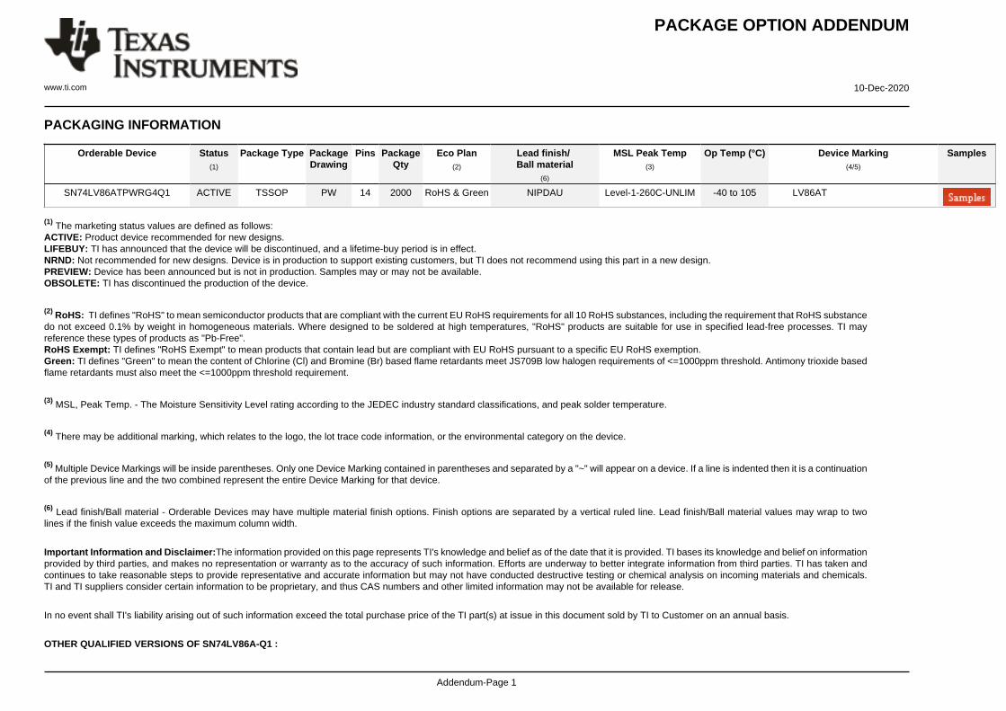
PACKAGE OPTION ADDENDUM
www.ti.com 10-Dec-2020
Addendum-Page 1
PACKAGING INFORMATION
Orderable Device Status(1)
Package Type PackageDrawing
Pins PackageQty
Eco Plan(2)
Lead finish/Ball material
(6)
MSL Peak Temp(3)
Op Temp (°C) Device Marking(4/5)
Samples
SN74LV86ATPWRG4Q1 ACTIVE TSSOP PW 14 2000 RoHS & Green NIPDAU Level-1-260C-UNLIM -40 to 105 LV86AT
(1) The marketing status values are defined as follows:ACTIVE: Product device recommended for new designs.LIFEBUY: TI has announced that the device will be discontinued, and a lifetime-buy period is in effect.NRND: Not recommended for new designs. Device is in production to support existing customers, but TI does not recommend using this part in a new design.PREVIEW: Device has been announced but is not in production. Samples may or may not be available.OBSOLETE: TI has discontinued the production of the device.
(2) RoHS: TI defines "RoHS" to mean semiconductor products that are compliant with the current EU RoHS requirements for all 10 RoHS substances, including the requirement that RoHS substancedo not exceed 0.1% by weight in homogeneous materials. Where designed to be soldered at high temperatures, "RoHS" products are suitable for use in specified lead-free processes. TI mayreference these types of products as "Pb-Free".RoHS Exempt: TI defines "RoHS Exempt" to mean products that contain lead but are compliant with EU RoHS pursuant to a specific EU RoHS exemption.Green: TI defines "Green" to mean the content of Chlorine (Cl) and Bromine (Br) based flame retardants meet JS709B low halogen requirements of <=1000ppm threshold. Antimony trioxide basedflame retardants must also meet the <=1000ppm threshold requirement.
(3) MSL, Peak Temp. - The Moisture Sensitivity Level rating according to the JEDEC industry standard classifications, and peak solder temperature.
(4) There may be additional marking, which relates to the logo, the lot trace code information, or the environmental category on the device.
(5) Multiple Device Markings will be inside parentheses. Only one Device Marking contained in parentheses and separated by a "~" will appear on a device. If a line is indented then it is a continuationof the previous line and the two combined represent the entire Device Marking for that device.
(6) Lead finish/Ball material - Orderable Devices may have multiple material finish options. Finish options are separated by a vertical ruled line. Lead finish/Ball material values may wrap to twolines if the finish value exceeds the maximum column width.
Important Information and Disclaimer:The information provided on this page represents TI's knowledge and belief as of the date that it is provided. TI bases its knowledge and belief on informationprovided by third parties, and makes no representation or warranty as to the accuracy of such information. Efforts are underway to better integrate information from third parties. TI has taken andcontinues to take reasonable steps to provide representative and accurate information but may not have conducted destructive testing or chemical analysis on incoming materials and chemicals.TI and TI suppliers consider certain information to be proprietary, and thus CAS numbers and other limited information may not be available for release.
In no event shall TI's liability arising out of such information exceed the total purchase price of the TI part(s) at issue in this document sold by TI to Customer on an annual basis.
OTHER QUALIFIED VERSIONS OF SN74LV86A-Q1 :
PACKAGE OPTION ADDENDUM
www.ti.com 10-Dec-2020
Addendum-Page 2
• Catalog: SN74LV86A
• Enhanced Product: SN74LV86A-EP
NOTE: Qualified Version Definitions:
• Catalog - TI's standard catalog product
• Enhanced Product - Supports Defense, Aerospace and Medical Applications
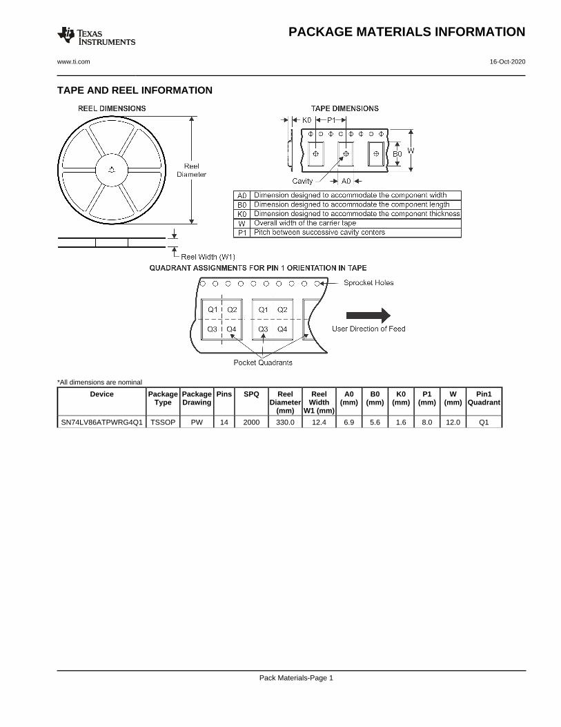
TAPE AND REEL INFORMATION
*All dimensions are nominal
Device PackageType
PackageDrawing
Pins SPQ ReelDiameter
(mm)
ReelWidth
W1 (mm)
A0(mm)
B0(mm)
K0(mm)
P1(mm)
W(mm)
Pin1Quadrant
SN74LV86ATPWRG4Q1 TSSOP PW 14 2000 330.0 12.4 6.9 5.6 1.6 8.0 12.0 Q1
PACKAGE MATERIALS INFORMATION
www.ti.com 16-Oct-2020
Pack Materials-Page 1
*All dimensions are nominal
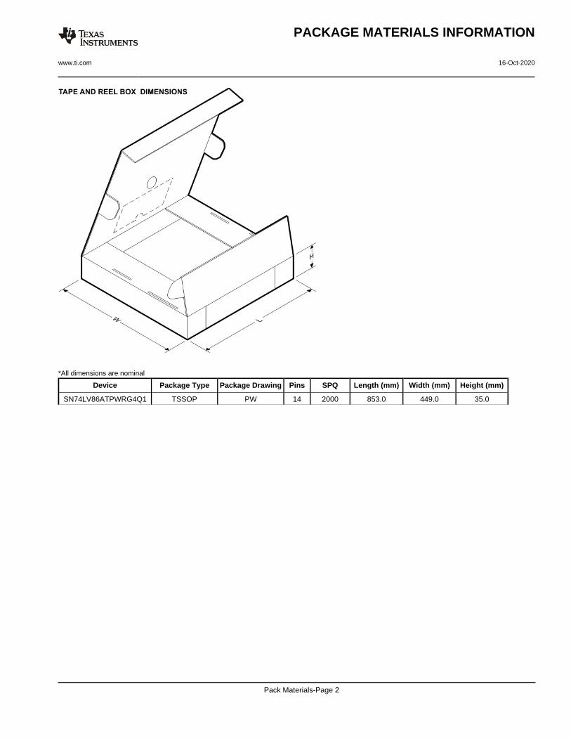
Device Package Type Package Drawing Pins SPQ Length (mm) Width (mm) Height (mm)
SN74LV86ATPWRG4Q1 TSSOP PW 14 2000 853.0 449.0 35.0
PACKAGE MATERIALS INFORMATION
www.ti.com 16-Oct-2020
Pack Materials-Page 2
IMPORTANT NOTICE AND DISCLAIMER
TI PROVIDES TECHNICAL AND RELIABILITY DATA (INCLUDING DATASHEETS), DESIGN RESOURCES (INCLUDING REFERENCE DESIGNS), APPLICATION OR OTHER DESIGN ADVICE, WEB TOOLS, SAFETY INFORMATION, AND OTHER RESOURCES “AS IS” AND WITH ALL FAULTS, AND DISCLAIMS ALL WARRANTIES, EXPRESS AND IMPLIED, INCLUDING WITHOUT LIMITATION ANY IMPLIED WARRANTIES OF MERCHANTABILITY, FITNESS FOR A PARTICULAR PURPOSE OR NON-INFRINGEMENT OF THIRD PARTY INTELLECTUAL PROPERTY RIGHTS.These resources are intended for skilled developers designing with TI products. You are solely responsible for (1) selecting the appropriate TI products for your application, (2) designing, validating and testing your application, and (3) ensuring your application meets applicable standards, and any other safety, security, or other requirements. These resources are subject to change without notice. TI grants you permission to use these resources only for development of an application that uses the TI products described in the resource. Other reproduction and display of these resources is prohibited. No license is granted to any other TI intellectual property right or to any third party intellectual property right. TI disclaims responsibility for, and you will fully indemnify TI and its representatives against, any claims, damages, costs, losses, and liabilities arising out of your use of these resources.TI’s products are provided subject to TI’s Terms of Sale (www.ti.com/legal/termsofsale.html) or other applicable terms available either on ti.com or provided in conjunction with such TI products. TI’s provision of these resources does not expand or otherwise alter TI’s applicable warranties or warranty disclaimers for TI products.
Mailing Address: Texas Instruments, Post Office Box 655303, Dallas, Texas 75265Copyright © 2020, Texas Instruments Incorporated