Embed Size (px)
Citation preview
FN7580Rev 3.00
December 14, 2015
ISL58792Laser Diode Driver with Serial Control and Write Current DAC
DATASHEET
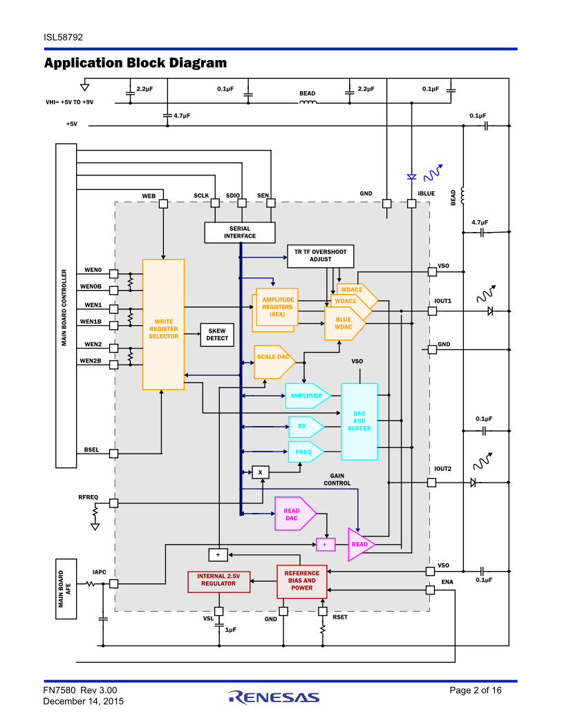
The ISL58792 is a highly integrated, single supply laser diode driver designed to support multi-standard writable optical drives in CD, DVD, and Blu-Ray formats at various speeds. It is a ‘hybrid’ part having an interface compatible with a conventional LDD, but an internal architecture similar to a write strategy LDD. This combination adds versatility to the conventional interface.
The rise time, fall time and overshoot of all outputs are adjustable to compensate for high and low resistance lasers.
The ISL58792 architecture includes dual write current banks, which can be selected using the bank select line, BSEL. This eliminates the need to synchronize the serial port to the media.
The oscillator is internally activated through program assignment to attach to any WEN state.
The WEN lines have internal 100 terminators. There is a skew detector on the WEN receiver outputs.
Applications• Combination DVD, CD, and Blue Writable Drives
• BD Camcorders
• BD Video Recorders
Features• Compatible with all Conventional Controllers Having a Serial
Port, with Some Programming
• Programmable Snubber on all Outputs
• Compatible with Future Controllers Having Gray Coded WEN Lines for Glitchless High-Speed Operation
• WEN Line Skew Detection
• 1000mA Maximum Total Write Output Current.
• 10-bit x 10-bit Multiplying DAC Output Provides 10-bit Full Scale Adjustment and 10-bit Resolution at any Full Scale Output
• Three Laser Outputs Allow Read/Write DVD, CD, and Blue Combinations
• Single +5V Supply
• Analog Inputs Supports Read APC
• HFM Oscillator Programmable to 100mAP-P and Range from 100MHz to >1GHz
• Programmable HFM On, Off and Cooling Levels
• Programmable Spread Spectrum for Low EMI
• Built-in ADC to Sample Laser Voltage Allows Power Reduction by Optimizing Headroom
• Built-in Thermal Sensor Aids in Thermal Design
• Serial Input Works up to 50MHz
• Pb-Free (RoHS Compliant)
FN7580 Rev 3.00 Page 1 of 16December 14, 2015
ISL58792
Application Block Diagram
GAINCONTROL
SERIAL INTERFACE
WRITE REGISTER SELECTOR
REFERENCE BIAS AND POWER
SCALE DAC
WDAC2
WDAC1
READDAC
AMPLITUDE
FREQ
OSCAND
BUFFER
SDIOSCLK SEN
BSEL
ENA
IAPC
GND
IOUT1
IBLUE
VSO
GND
READ
BLUEWDAC
VSO
IOUT2
VSL
WEN0
WEN0B
WEN1
WEN1B
WEN2
WEN2B
MA
IN B
OA
RD
CO
NTR
OLL
ERM
AIN
BO
AR
DA
FE
SS
0.1µF
2.2µF0.1µF
0.1µF
0.1µF4.7µF
4.7µF
+5V
X
SKEW DETECT
RSET
GND
2.2µFBEAD
BEA
D
0.1µF
TR TF OVERSHOOTADJUST
RFREQ
WEB
AMPLITUDE REGISTERS
(8EA)
+
+
1µF
VHI= +5V TO +9V
VSO
INTERNAL 2.5V REGULATOR
FN7580 Rev 3.00 Page 2 of 16December 14, 2015
ISL58792
Pin ConfigurationISL58792
(24 LD TQFN)TOP VIEW
Ordering Information
PART NUMBER(Note 2)
PARTMARKING
TEMP RANGE(°C)
PACKAGETape & Reel
(Pb-free)PKG.
DWG.#
ISL58792CRTZ 587 92CRTZ -10 to +85 24 Ld TQFN L24.4x4E
ISL58792CRTZ-T13 (Note 1) 587 92CRTZ -10 to +85 24 Ld TQFN L24.4x4E
ISL58792CRTZ-T7A (Note 1) 587 92CRTZ -10 to +85 24 Ld TQFN L24.4x4E
1. Please refer to TB347 for details on reel specifications.
2. These Intersil Pb-free plastic packaged products employ special Pb-free material sets, molding compounds/die attach materials, and 100% matte tin plate plus anneal (e3 termination finish, which is RoHS compliant and compatible with both SnPb and Pb-free soldering operations). Intersil Pb-free products are MSL classified at Pb-free peak reflow temperatures that meet or exceed the Pb-free requirements of IPC/JEDEC J STD-020.
THERMAL PAD
18
17
16
15
14
24 23 22 21 201
2
3
4
5
6
WEN0
WEN0B
WEN1
WEN1B
WEN2
VSO
IOUT1
GND
IOUT2
VSO
SCLK
SDIO
SEN
GN
D
BSE
L
RFR
EQ
IAP
C
VSL
GN
D
13
19
ENA
RSE
T
WEN2B
IBLU
E
WEB
1211
10987
Pin DescriptionsPIN
NAMEPIN
NUMBER I/OPIN
TYPE PIN DESCRIPTION
WEN0, WEN0B
1, 2 I LVDS Write Enable 0. When WEN0 > WEN0B, the result is a logic 1 in the write current selection. Otherwise it is logic 0.
WEN1, WEN1B
3, 4 I LVDS Write Enable 1. When WEN1 > WEN1B, the result is a logic 1 in the write current selection. Otherwise it is logic 0.
WEN2, WEN2B
5, 6 I LVDS Write Enable 2. When WEN2 > WEN2B, the result is a logic 1 in the write current selection. Otherwise it is logic 0.
BSEL 7 I Digital Bank Select input selects the write current register banks.
RFREQ 8 I/O Analog A resistor from RFREQ to GND sets the range of the HFM frequency.
IAPC 9 I Analog A 1k impedance current input; 100*IAPC flows to the output. This controls the read current, which may also include a current from an internal DAC.
VSL 10 O Power The internal 2.5V regulator; a 1µF capacitor from VSL to GND is recommended. Do not use VSL for other loads.
GND 11, 16, 20 Ground Ground
RSET 12 I/O Analog A resistor from RSET to analog ground sets the DAC full-scale current.
FN7580 Rev 3.00 Page 3 of 16December 14, 2015
ISL58792
ENA 13 I Digital Chip enable input (H = enable, L = disable)
VSO 14, 18 Power Supply voltage. (connect all pins)
IOUT2 15 O Analog Laser diode output #2
IOUT1 17 O Analog Laser diode output #1
IBLUE 19 O Analog Blue laser diode output
SEN 21 I Digital Serial control enable (H = enable, L = disable)
SDIO 22 I/O Digital Serial data for parameters and control; in/out
SCLK 23 I Digital Serial control clock
WEB 24 I Digital Write enable Bar. When low, write current is enabled.
PD Thermal The Thermal pad should be grounded and connected to a heat sink.
NOTE: Pins with the same name are internally connected together; however, LDD pins must not be used for connecting together external components or features.
Pin Descriptions (Continued)
PIN NAME
PINNUMBER I/O
PIN TYPE PIN DESCRIPTION
FN7580 Rev 3.00 Page 4 of 16December 14, 2015
ISL58792
IMPORTANT NOTE: All parameters having Min/Max specifications are guaranteed. Typical values are for information purposes only. Unless otherwisenoted, all tests are at the specified temperature and are pulsed tests, therefore: TJ = TC = TA
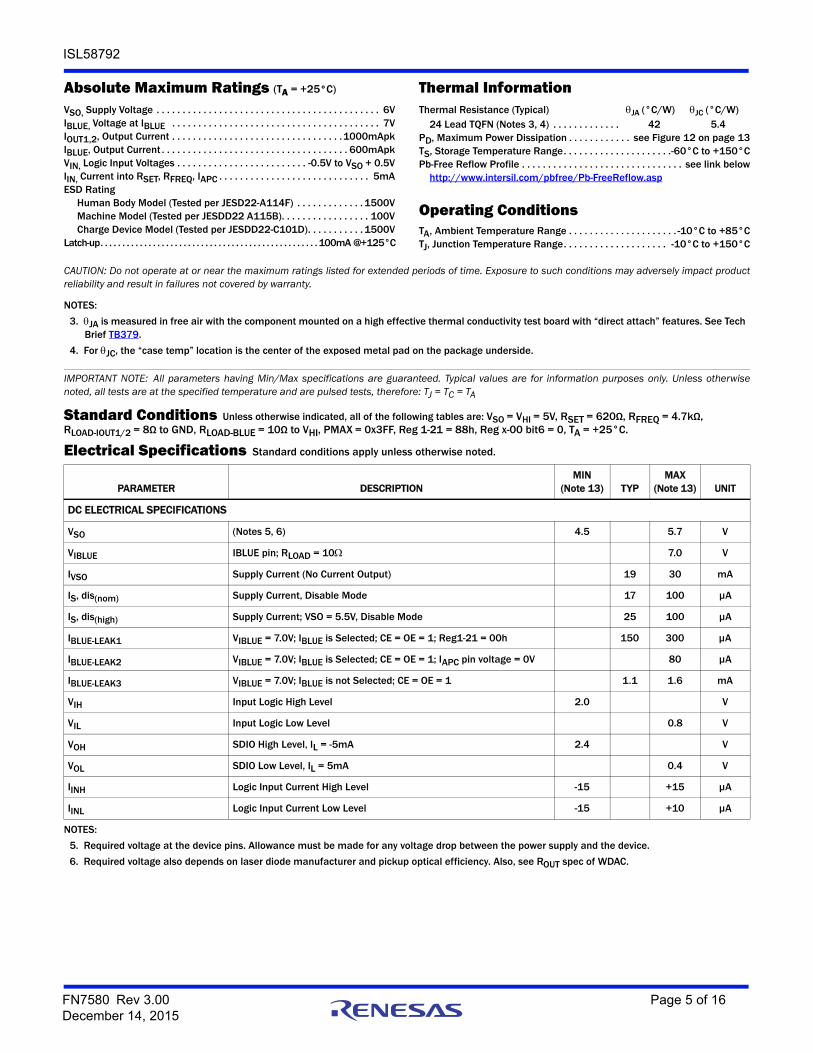
Standard Conditions Unless otherwise indicated, all of the following tables are: VSO = VHI = 5V, RSET = 620Ω, RFREQ = 4.7kΩ, RLOAD-IOUT1/2 = 8Ω to GND, RLOAD-BLUE = 10Ω to VHI, PMAX = 0x3FF, Reg 1-21 = 88h, Reg x-00 bit6 = 0, TA = +25°C.
Absolute Maximum Ratings (TA = +25°C) Thermal InformationVSO, Supply Voltage . . . . . . . . . . . . . . . . . . . . . . . . . . . . . . . . . . . . . . . . . . . 6VIBLUE, Voltage at IBLUE . . . . . . . . . . . . . . . . . . . . . . . . . . . . . . . . . . . . . . . . 7VIOUT1,2, Output Current . . . . . . . . . . . . . . . . . . . . . . . . . . . . . . . . .1000mApkIBLUE, Output Current . . . . . . . . . . . . . . . . . . . . . . . . . . . . . . . . . . . . 600mApkVIN, Logic Input Voltages . . . . . . . . . . . . . . . . . . . . . . . . . -0.5V to VSO + 0.5VIIN, Current into RSET, RFREQ, IAPC . . . . . . . . . . . . . . . . . . . . . . . . . . . . . 5mAESD Rating
Human Body Model (Tested per JESD22-A114F) . . . . . . . . . . . . . 1500VMachine Model (Tested per JESDD22 A115B). . . . . . . . . . . . . . . . . 100VCharge Device Model (Tested per JESDD22-C101D). . . . . . . . . . . 1500V
Latch-up. . . . . . . . . . . . . . . . . . . . . . . . . . . . . . . . . . . . . . . . . . . . . . . . . . 100mA @+125°C
Thermal Resistance (Typical) JA (°C/W) JC (°C/W)24 Lead TQFN (Notes 3, 4) . . . . . . . . . . . . . 42 5.4
PD, Maximum Power Dissipation . . . . . . . . . . . . see Figure 12 on page 13TS, Storage Temperature Range. . . . . . . . . . . . . . . . . . . . .-60°C to +150°CPb-Free Reflow Profile . . . . . . . . . . . . . . . . . . . . . . . . . . . . . . . see link below
http://www.intersil.com/pbfree/Pb-FreeReflow.asp
Operating ConditionsTA, Ambient Temperature Range . . . . . . . . . . . . . . . . . . . . . -10°C to +85°CTJ, Junction Temperature Range. . . . . . . . . . . . . . . . . . . . -10°C to +150°C
CAUTION: Do not operate at or near the maximum ratings listed for extended periods of time. Exposure to such conditions may adversely impact productreliability and result in failures not covered by warranty.
NOTES:
3. JA is measured in free air with the component mounted on a high effective thermal conductivity test board with “direct attach” features. See Tech Brief TB379.
4. For JC, the “case temp” location is the center of the exposed metal pad on the package underside.
Electrical Specifications Standard conditions apply unless otherwise noted.
PARAMETER DESCRIPTIONMIN
(Note 13) TYPMAX
(Note 13) UNIT
DC ELECTRICAL SPECIFICATIONS
VSO (Notes 5, 6) 4.5 5.7 V
VIBLUE IBLUE pin; RLOAD = 10 7.0 V
IVSO Supply Current (No Current Output) 19 30 mA
IS, dis(nom) Supply Current, Disable Mode 17 100 µA
IS, dis(high) Supply Current; VSO = 5.5V, Disable Mode 25 100 µA
IBLUE-LEAK1 VIBLUE = 7.0V; IBLUE is Selected; CE = OE = 1; Reg1-21 = 00h 150 300 µA
IBLUE-LEAK2 VIBLUE = 7.0V; IBLUE is Selected; CE = OE = 1; IAPC pin voltage = 0V 80 µA
IBLUE-LEAK3 VIBLUE = 7.0V; IBLUE is not Selected; CE = OE = 1 1.1 1.6 mA
VIH Input Logic High Level 2.0 V
VIL Input Logic Low Level 0.8 V
VOH SDIO High Level, IL = -5mA 2.4 V
VOL SDIO Low Level, IL = 5mA 0.4 V
IINH Logic Input Current High Level -15 +15 µA
IINL Logic Input Current Low Level -15 +10 µA
NOTES:
5. Required voltage at the device pins. Allowance must be made for any voltage drop between the power supply and the device.
6. Required voltage also depends on laser diode manufacturer and pickup optical efficiency. Also, see ROUT spec of WDAC.
FN7580 Rev 3.00 Page 5 of 16December 14, 2015
ISL58792
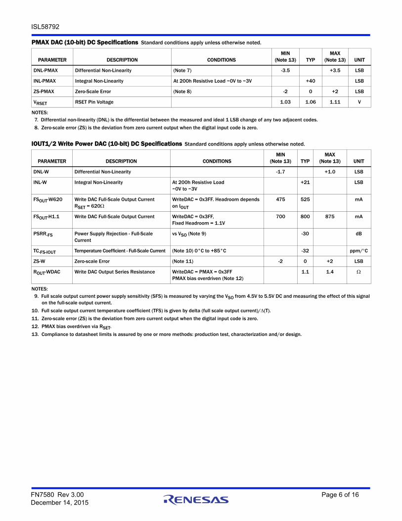
PMAX DAC (10-bit) DC Specifications Standard conditions apply unless otherwise noted.
PARAMETER DESCRIPTION CONDITIONSMIN
(Note 13) TYPMAX
(Note 13) UNIT
DNL-PMAX Differential Non-Linearity (Note 7) -3.5 +3.5 LSB
INL-PMAX Integral Non-Linearity At 200h Resistive Load ~0V to ~3V +40 LSB
ZS-PMAX Zero-Scale Error (Note 8) -2 0 +2 LSB
VRSET RSET Pin Voltage 1.03 1.06 1.11 V
NOTES:7. Differential non-linearity (DNL) is the differential between the measured and ideal 1 LSB change of any two adjacent codes.
8. Zero-scale error (ZS) is the deviation from zero current output when the digital input code is zero.
IOUT1/2 Write Power DAC (10-bit) DC Specifications Standard conditions apply unless otherwise noted.
PARAMETER DESCRIPTION CONDITIONSMIN
(Note 13) TYPMAX
(Note 13) UNIT
DNL-W Differential Non-Linearity -1.7 +1.0 LSB
INL-W Integral Non-Linearity At 200h Resistive Load ~0V to ~3V
+21 LSB
FSOUT-W620 Write DAC Full-Scale Output Current RSET = 620
WriteDAC = 0x3FF. Headroom depends on IOUT
475 525 mA
FSOUT-H1.1 Write DAC Full-Scale Output Current WriteDAC = 0x3FF, Fixed Headroom = 1.1V
700 800 875 mA
PSRR-FS Power Supply Rejection - Full-Scale Current
vs VSO (Note 9) -30 dB
TC-FS-IOUT Temperature Coefficient - Full-Scale Current (Note 10) 0°C to +85°C -32 ppm/C
ZS-W Zero-scale Error (Note 11) -2 0 +2 LSB
ROUT-WDAC Write DAC Output Series Resistance WriteDAC = PMAX = 0x3FFPMAX bias overdriven (Note 12)
1.1 1.4
NOTES:9. Full scale output current power supply sensitivity (SFS) is measured by varying the VSO from 4.5V to 5.5V DC and measuring the effect of this signal
on the full-scale output current.
10. Full scale output current temperature coefficient (TFS) is given by delta (full scale output current)/(T).
11. Zero-scale error (ZS) is the deviation from zero current output when the digital input code is zero.
12. PMAX bias overdriven via RSET.
13. Compliance to datasheet limits is assured by one or more methods: production test, characterization and/or design.
FN7580 Rev 3.00 Page 6 of 16December 14, 2015
ISL58792
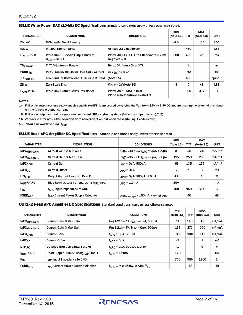
IBLUE Write Power DAC (10-bit) DC Specifications Standard conditions apply unless otherwise noted.
PARAMETER DESCRIPTION CONDITIONSMIN
(Note 13) TYPMAX
(Note 13) UNIT
DNL-W Differential Non-Linearity -4.9 +2.0 LSB
INL-W Integral Non-Linearity At fixed 2.5V headroom +60 LSB
FSOUT-H2.0 Write DAC Full-Scale Output CurrentRSET = 620
WriteDAC = 0x3FF; Fixed Headroom = 2.0V; Reg 1-21 = 8F
380 450 575 mA
TRRANGE Tr Tf Adjustment Range Reg 1-0A from X0h to X7h 1 ns
PSRR-FS Power Supply Rejection - Full-Scale Current vs VSO (Note 14) -40 dB
TCFS-IBLUE Temperature Coefficient - Full-Scale Current (Note 15) 600 ppm/C
ZS-W Zero-Scale Error VIOUT = 2V (Note 16) -8 0 +8 LSB
ROUT-WDAC Write DAC Output Series Resistance WriteDAC = PMAX = 0x3FFPMAX bias overdriven (Note 17)
3.4 4.5
NOTES:14. Full scale output current power supply sensitivity (SFS) is measured by varying the VSO from 4.5V to 5.5V DC and measuring the effect of this signal
on the full-scale output current.
15. Full scale output current temperature coefficient (TFS) is given by delta (full scale output current)/(T).
16. Zero-scale error (ZS) is the deviation from zero current output when the digital input code is zero.
17. PMAX bias overdriven via RSET.
IBLUE Read APC Amplifier DC Specifications Standard conditions apply unless otherwise noted.
PARAMETER DESCRIPTION CONDITIONSMIN
(Note 13) TYPMAX
(Note 13) UNIT
IAPCMIN-GAIN Current Gain @ Min Gain Reg1-21h = 1X, IAPC = 0µA, 500µA 8 15 25 mA/mA
IAPCMAX-GAIN Current Gain @ Max Gain Reg1-21h = FX, IAPC = 0µA, 500µA 195 250 295 mA/mA
IAPCGAIN Current Gain IAPC = 0µA, 500µA 95 135 175 mA/mA
IAPCOS Current Offset IAPC = 0µA -2 1 3 mA
LINAPC Output Current Linearity; Best Fit IAPC = 0µA, 500µA, 1.0mA -12 1 %
IOUT-R-APC Blue Read Output Current, Using IAPC Input IAPC = 1.5mA 150 mA
RIN IAPC Input Impedance to GND 700 950 1200
PSRRAPC IAPC Current Power Supply Rejection IOUT-average = 100mA, varying VSO -46 dB
OUT1/2 Read APC Amplifier DC Specifications Standard conditions apply unless otherwise noted.
PARAMETER DESCRIPTION CONDITIONSMIN
(Note 13) TYPMAX
(Note 13) UNIT
IAPCMIN-GAIN Current Gain @ Min Gain Reg1-21h = 1X, IAPC = 0µA, 500µA 11 14.5 19 mA/mA
IAPCMAX-GAIN Current Gain @ Max Gain Reg1-21h = FX, IAPC = 0µA, 500µA 155 173 200 mA/mA
IAPCGAIN Current Gain IAPC = 0µA, 500µA 85 100 115 mA/mA
IAPCOS Current Offset IAPC = 0µA -2 1 3 mA
LINAPC Output Current Linearity; Best Fit IAPC = 0µA, 500µA, 1.0mA -1 6 %
IOUT-R-APC Read Output Current, Using IAPC Input IAPC = 1.5mA 120 mA
RIN IAPC Input Impedance to GND 700 950 1200
PSRRAPC IAPC Current Power Supply Rejection IAPC-IN = 0.45mA, varying VSO -48 dB
FN7580 Rev 3.00 Page 7 of 16December 14, 2015
ISL58792
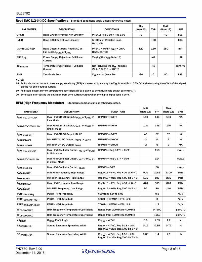
Read DAC (12-bit) DC Specifications Standard conditions apply unless otherwise noted.
PARAMETER DESCRIPTION CONDITIONSMIN
(Note 13) TYPMAX
(Note 13) UNIT
DNL-R Read DAC Differential Non-Linearity PREAD: Reg 0-19 + Reg 1-09 -2 +2 LSB
INL-R Read DAC Integral Non-Linearity @ 900h on Resistive Load. 0V to ~3V
+90 LSB
IOUT-R-DAC-RED Read Output Current, Read DAC at Full-Scale, IOUT1 or IOUT2
PREAD = 0xFFF, IAPC = 0mA,Reg 1-21 = 8F
120 150 180 mA
PSRR-FS Power Supply Rejection - Full-Scale Current
Varying the VSO (Note 18) -42 dB
TC-FS-IOUT Temperature Coefficient - Full-Scale Current
Not including the RSET tempco (Note 19) 0°C to +85°C
-48 ppm/C
ZS-R Zero-Scale Error VIOUT = 2V (Note 20) -80 0 80 LSB
NOTES:18. Full scale output current power supply sensitivity (SFS) is measured by varying the VSO from 4.5V to 5.5V DC and measuring the effect of this signal
on the full-scale output current.
19. Full scale output current temperature coefficient (TFS) is given by delta (full scale output current)/(T).
20. Zero-scale error (ZS) is the deviation from zero current output when the digital input code is zero.
HFM (High Frequency Modulator) Standard conditions unless otherwise noted.
PARAMETER DESCRIPTION CONDITIONSMIN
(Note 13) TYPMAX
(Note 13) UNIT
IMAX-RED-OFF-LINK Max HFM Off DC Output, IOUT1 or IOUT2 in Link Mode
HFMOFF = 0xFFF 110 145 180 mA
IMAX-RED-OFF-UNLINK Max HFM Off DC Output, IOUT1 or IOUT2 in Unlink Mode
HFMOFF = 0xFFF 100 135 170 mA
IMAX-BLUE-OFF Max HFM Off DC Output, IBLUE HFMOFF = 0xFFF 45 62 75 mA
IMIN-RED-OFF Min HFM Off DC Output, IOUT1 or IOUT2 HFMOFF = 0x000 -3 0 3 mA
IMIN-BLUE-OFF Min HFM Off DC Output, IBLUE HFMOFF = 0x000 -3 0 3 mA
IMAX-RED-ON-LINK Max HFM Oscillator Output, IOUT1 or IOUT2 in Link Mode
HFMON = Reg 0-17h = 0xFF 118 mAP-P
IMAX-RED-ON-UNLINK Max HFM Oscillator Output, IOUT1 or IOUT2 in Unlink Mode
HFMON = Reg 0-17h = 0xFF 114 mAP-P
IMAX-BLUE-ON Max HFM Oscillator Output, IBLUE HFMON = 0xFF 60 mAP-P
FOSC-HI-MAX Max HFM Frequency, High Range Reg 0-16 = FFh, Reg X-00 bit 6 = 0 900 1086 1300 MHz
FOSC-HI-MIN Min HFM Frequency, High Range Reg 0-16 = 01h, Reg X-00 bit 6 = 0 135 190 255 MHz
FOSC-LO-MAX Max HFM Frequency, Low Range Reg 0-16 = FFh, Reg X-00 bit 6 =1 470 565 670 MHz
FOSC-LO-MIN Min HFM Frequency, Low Range Reg 0-16 = 01h, Reg X-00 bit 6 = 1 55 80 110 MHz
PSRROSC-FREQ PSRR - HFM Frequency VSO from 4.5V to 5.0V 0.5 %/V
PSRROSC-AMP-IOUT PSRR - HFM Amplitude 350MHz; HFMON = FFh; Link 3 %/V
PSRROSC-AMP-IBLUE PSRR - HFM Amplitude 700MHz; HFMON = FFh; Link 1.2 %/V
TFOSC400MAX HFM Frequency Temperature Coefficient Range from 200MHz to 400MHz 0 - 900 ppm/C
TFOSC900MAX HFM Frequency Temperature Coefficient Range from 400MHz to 900MHz ±250 ppm/C
VRFREQ RFREQ Pin Voltage RFREQ = 4.7k 0.9 1.03 1.2 V
SS-WIDTH-10h Spread Spectrum Spreading Width RFREQ = 4.7kReg 1-18 = 10h, Reg 0-16 = 26h; Reg X-00 bit 6 = 0
0.15 0.35 0.75 %
SS-WIDTH-70h Spread Spectrum Spreading Width RFREQ = 4.7kReg 1-18 = 70h, Reg 0-16 = 26h; Reg X-00 bit 6 = 0
0.65 1.4 2.1 %
FN7580 Rev 3.00 Page 8 of 16December 14, 2015
ISL58792
SS-WIDTH-78h Spread Spectrum Spreading Width RFREQ = 4.7kReg 1-18 = 78h, Reg 0-16 = 26h; Reg X-00 bit 6 = 0
1.7 2.8 4 %
SS_Shift Shift of Center Frequency when SS is Enabled vs when it’s Disabled
RFREQ = 4.7kReg 1-18 = 00h to 40h, Reg 0-16 = 26h; Reg X-00 bit 6 = 0
1.4 %
SS_Mod Spread Spectrum Modulation Frequency REG 1-18h Bit 7 = 0; Reg X-00 bit 6 = 0
50 76 105 kHz
SS_Mod Spread Spectrum Modulation Frequency REG 1-18h Bit 7 = 1; Reg X-00 bit 6 = 0
25 44 65 kHz
HFM (High Frequency Modulator) Standard conditions unless otherwise noted. (Continued)
PARAMETER DESCRIPTION CONDITIONSMIN
(Note 13) TYPMAX
(Note 13) UNIT
Serial Interface AC Performance Standard conditions unless otherwise noted.
PARAMETER DESCRIPTION CONDITIONSMIN
(Note 13) TYPMAX
(Note 13) UNIT
FSER SCLK Operating Range Static logic not limited at low frequency 50 MHz
tEH SEN “H” Time @ 50MHz 320 ns
tEL SEN “L” Time @ 50MHz 160 ns
tERSR SEN Rising Edge to the First SCLK Rising Edge @ 50MHz 10 ns
tCDS SDIO Set Up Time @ 50MHz 10 ns
tCDH SDIO Hold Time @ 50MHz 10 ns
tSREF Last SCLK Rising Edge to SEN Falling Edge @ 50MHz 10 ns
tCC SCLK Cycle Time1 @ 50MHz 20 ns
Duty SCLK “H” Duty Cycle @ 50MHz 40 50 60 %
tCDD SDIO Output Delay @ 50MHz 4 ns
tEDH SDIO Output Hold Time @ 50MHz 2 ns
LVDS Specifications Standard conditions unless otherwise noted.
PARAMETER DESCRIPTION CONDITIONSMIN
(Note 13) TYPMAX
(Note 13) UNIT
VIN-HIGH Maximum Single Line Voltage 2.4 V
VIN-LOW Minimum Single Line Voltage 0 V
RIN Input Resistance 85 100 115
VMIN Minimum Differential Voltage Signal tested with ±240mV differential input 240 mVPK
FN7580 Rev 3.00 Page 9 of 16December 14, 2015
ISL58792
Laser Driver AC Performance Demo board test, 10% duty cycle pulse, load = equivalent circuitry to [laser + flex cable] and/or as noted. VSO = 5V. TA = +25°C
PARAMETER DESCRIPTION CONDITIONS MIN TYP MAX UNIT
tR-IOUTx IOUT1/2 Write Rise Time (10% to 90%) 300mW Optical ML229U7 1.3 ns
tF-IOUTx IOUT1/2 Write Fall Time (10% to 90%) 300mW Optical ML229U7 800 ps
O/S-IOUTx IOUT1/2 Write Pulse Overshoot 300mW Optical ML229U7 11 %
tD-IOUTx IOUT1/2 Write Pulse Delay From LVDS = Zero crossing to IOUT rise 10%
5.3 ns
tR-BLUE IBLUE Write Rise Time (10% to 90%) 300mW Optical 650 ps
tF-BLUE IBLUE Write Fall Time (10% to 90%) 300mW Optical 450 ps
O/S-BLUE IBLUE Write Pulse Overshoot 300mW Rising Optical 12 %
tD-BLUE IBLUE Write Pulse Delay From LVDS = Zero crossing to IOUT rise 10%
5.2 ns
INOISE-IOUTx IOUT1/2 Read Output Current Noise IOUT = 50mA, measured @ 10MHz 0.55 nA/Hz
INOISE-IOUTx IOUT1/2 Read and HFM Output Current Noise IOUT = 50mA+30mAP-P; measured @ 10MHz 0.96 nA/Hz
INOISE-BLUE IBLUE Read Output Current Noise IOUT = 50mA, measured @ 10MHz 0.37 nA/Hz
INOISE-BLUE IBLUE Read and HFM Output Current Noise IOUT = 50mA+10mAP-P; measured @ 10MHz 0.47 nA/Hz
BWAPC Read Amplifier 3dB Bandwidth IOUT = 50mA 0.5 MHz
TABLE 1. AMPLITUDE SELECTION REGISTER ACTIVATION
NAME ENA WEBCR0Bit 2 WEN2 WEN1 WEN0
MSB BSEL = 0
LSB BSEL = 0
MSB BSEL = 1
LSB BSEL = 1
OFF 0 X x X X X X X X X
READ 1 1 0 X X X 0-19 1-09 0-19 1-09
W0 1 0 1 0 0 0 0-10 2-10 0-11 2-11
W1 1 0 1 0 0 1 0-04 2-04 0-05 2-05
W2 1 0 1 0 1 0 0-06 2-06 0-07 2-07
W3 1 0 1 0 1 1 0-08 2-08 0-09 2-09
W4 1 0 1 1 0 0 0-0A 2-0A 0-0B 2-0B
W5 1 0 1 1 0 1 0-0C 2-0C 0-0D 2-0D
W6 1 0 1 1 1 0 0-0E 2-0E 0-0F 2-0F
W7 1 0 1 1 1 1 0-12 2-12 0-13 2-13
NOTES:
21. There are two sets of write current registers. When BSEL = 1, bank 1 is selected. When BSEL = 0, bank 0 is selected.
22. Read and write are independent. Read is enabled with a control bit.
23. Register terminology is page Number-Register number (hex). Thus 1-09 is page 1, register 09h.
FN7580 Rev 3.00 Page 10 of 16December 14, 2015
ISL58792
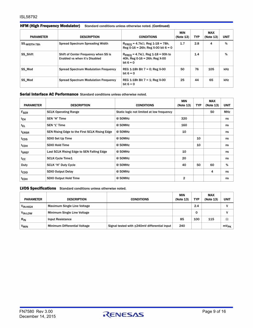
Applications InformationIOUTThe data sheet values for oscillator current, and write current are based on an RSET of 620 when PMAX and WriteDAC are both set to full scale. The user may choose RSET to match the output current needs of the application.
The PMAX DAC is biased by IRSET (= VRSET/RSET). See the “Typical Performance Curves” on page 11.
The write channel output capability for a typical part is shown in Figures 1, 2, and 3. The amount of IOUT will be limited by the available headroom voltage at the IOUTx pins.
A four input DAC (Reg 1-0A bits 3, 2, 1, 0) can be used to control the amount of RC snubbing applied to the outputs. For IBLUE, there is an extra bit (Reg 1-0A bit 4) weighted as MSB.
Read current may be controlled by either the Read DAC or the IAPC input. When set by the PREAD DAC, IREAD is limited to the data sheet value, whereas the IAPC input will allow a significantly higher value to be obtained. The ReadDAC and IAPC currents sum together.
Glitches could occur if two or three WEN lines are changed simultaneously, and the propagation delay is different for the two lines between the inner circuits of the controller and the inner circuits of the LDD. Because the WEN lines are encoded, the selected write current will be correct before the change in code, and again after the code changes. But some other output could result momentarily if the propagation delays are not matched. The skew detector detects the first rising edge at the LVDS outputs.
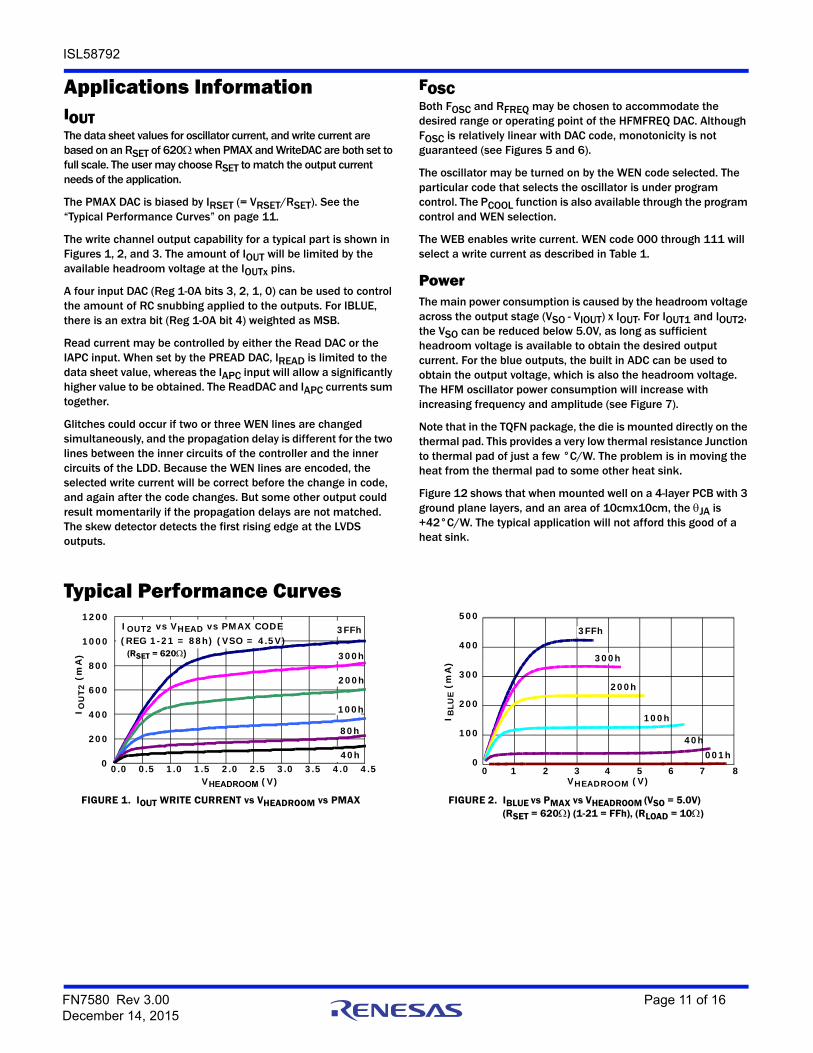
FOSC Both FOSC and RFREQ may be chosen to accommodate the desired range or operating point of the HFMFREQ DAC. Although FOSC is relatively linear with DAC code, monotonicity is not guaranteed (see Figures 5 and 6).
The oscillator may be turned on by the WEN code selected. The particular code that selects the oscillator is under program control. The PCOOL function is also available through the program control and WEN selection.
The WEB enables write current. WEN code 000 through 111 will select a write current as described in Table 1.
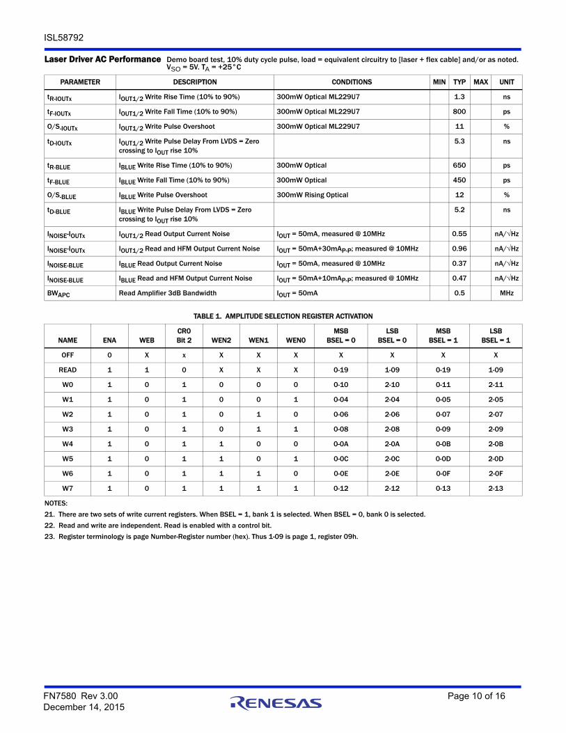
Power The main power consumption is caused by the headroom voltage across the output stage (VSO - VIOUT) x IOUT. For IOUT1 and IOUT2, the VSO can be reduced below 5.0V, as long as sufficient headroom voltage is available to obtain the desired output current. For the blue outputs, the built in ADC can be used to obtain the output voltage, which is also the headroom voltage. The HFM oscillator power consumption will increase with increasing frequency and amplitude (see Figure 7).
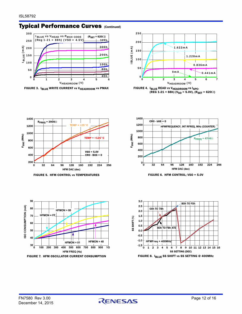
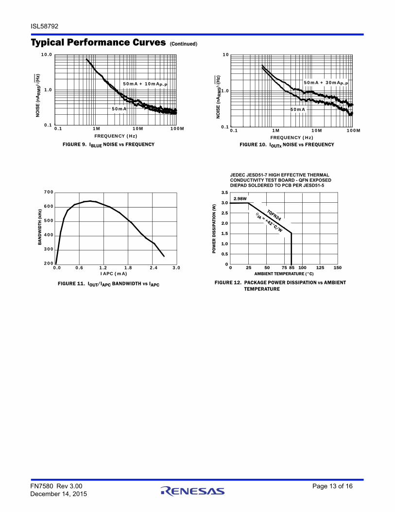
Note that in the TQFN package, the die is mounted directly on the thermal pad. This provides a very low thermal resistance Junction to thermal pad of just a few °C/W. The problem is in moving the heat from the thermal pad to some other heat sink.
Figure 12 shows that when mounted well on a 4-layer PCB with 3 ground plane layers, and an area of 10cmx10cm, the JA is +42°C/W. The typical application will not afford this good of a heat sink.
Typical Performance Curves
FIGURE 1. IOUT WRITE CURRENT vs VHEADROOM vs PMAX FIGURE 2. IBLUE vs PMAX vs VHEADROOM (VSO = 5.0V) (RSET = 620) (1-21 = FFh), (RLOAD = 10)
VHEADROOM (V)
I OU
T2 (
mA
)
(REG 1-21 = 88h) (VSO = 4.5V)IOUT2 vs VHEAD vs PMAX CODE 3FFh
300h
200h
100h
80h
40h0.0 0.5 1.0 1.5 2.0 2.5 3.0 3.5 4.0 4.50
200
400
600
800
1000
1200
(RSET = 620)
0 2 5 7VHEADROOM (V)
1 3 4 6 8
3FFh
300h
200h
100h
40h001h
I BLU
E (m
A)
0
100
200
300
400
500
FN7580 Rev 3.00 Page 11 of 16December 14, 2015
ISL58792
FIGURE 3. IBLUE WRITE CURRENT vs VHEADROOM vs PMAX FIGURE 4. IBLUE READ vs VHEADROOM vs IAPC, (REG 1-21 = 88h) (VSO = 5.0V), (RSET = 620)
FIGURE 5. HFM CONTROL vs TEMPERATURES FIGURE 6. HFM CONTROL; VSO = 5.0V
FIGURE 7. HFM OSCILLATOR CURRENT CONSUMPTION FIGURE 8. IBLUE SS SHIFT vs SS SETTING @ 400MHz
Typical Performance Curves (Continued)
0
50
100
150
200
250
300
0 1 2 3 4 5 6VHEADROOM (V)
I BLU
E (m
A) 300h
100h
80h
40h
200h
3FFh(RSET = 620)IBLUE vs VHEAD vs PMAX CODE
(Reg 1-21 = 88h) (VSO = 4.5V)
0
50
100
150
200
250
0 1 2 3 4 5 6 7VHEADROOM (V)
IBLU
E (
mA
)
0.441mA
0.836mA
1.228mA
1.622mA
0mA
200
400
600
800
1000
1200
1400
0 32 64 96 128 160 192 224 256
HFM DAC (dec)
RFREQ = 3900TEMP = +25°C
VSO = 5.0VCR0 - Bit6 = 0
TEMP = +125°C
F OSC
(MH
z)
0
200
400
600
800
1000
1200
1400
0 32 64 96 128 160 192 224 256
HFM DAC (dec)
HFMFREQUENCY, INT RFREQ, MHz (COUNTER)
F OSC
(MH
z)
CR0 - bit6 = 0
RFREQ = 4700
30
40
50
60
70
80
90
0 100 200 300 400 500 600 700 800 900 1G
HFM FREQ (Hz)
ISO
CO
NS
UM
PT
ION
(m
A)
HFMON = 40HFMON = 01
HFMON = 80
HFMON = FF
-1.5
-1.0
-0.5
0.0
0.5
1.0
1.5
2.0
2.5
3.0
0 1 2 3 4 5 6 7 8 9 10 11 12 13 14 15 16
00h TO 78h
80h TO F8h ATE
80h TO F0h
SS S
HIF
T (%
)
SS SETTING (DEC)
HFMFreq = 400MHz
FN7580 Rev 3.00 Page 12 of 16December 14, 2015
ISL58792
FIGURE 9. IBLUE NOISE vs FREQUENCY FIGURE 10. IOUTx NOISE vs FREQUENCY
FIGURE 11. IOUT/IAPC BANDWIDTH vs IAPC FIGURE 12. PACKAGE POWER DISSIPATION vs AMBIENT TEMPERATURE
Typical Performance Curves (Continued)
0.1
1.0
10.0
0.1 1M 10M 100MFREQUENCY (Hz)
50mA + 10mAP-P
50mA
NO
ISE
(n
AR
MS
/(H
z)
0.1
1.0
10
0.1 1M 10M 100MFREQUENCY (Hz)
NO
ISE
(n
AR
MS
/(H
z)
50mA + 30mAP-P
50mA
700
600
500
400
300
2000.0 0.6 1.2 1.8 2.4 3.0
IAPC (mA)
BA
ND
WID
TH (k
Hz)
3.0
2.0
1.0
0.5
00 25 50 75 100
3.5
2.5
1.5
125 150
JEDEC JESD51-7 HIGH EFFECTIVE THERMAL CONDUCTIVITY TEST BOARD - QFN EXPOSED DIEPAD SOLDERED TO PCB PER JESD51-5
AMBIENT TEMPERATURE (°C)
2.98W
JA = +42°C/W
TQFN24P
OW
ER D
ISSI
PATI
ON
(W)
85
FN7580 Rev 3.00 Page 13 of 16December 14, 2015
ISL58792
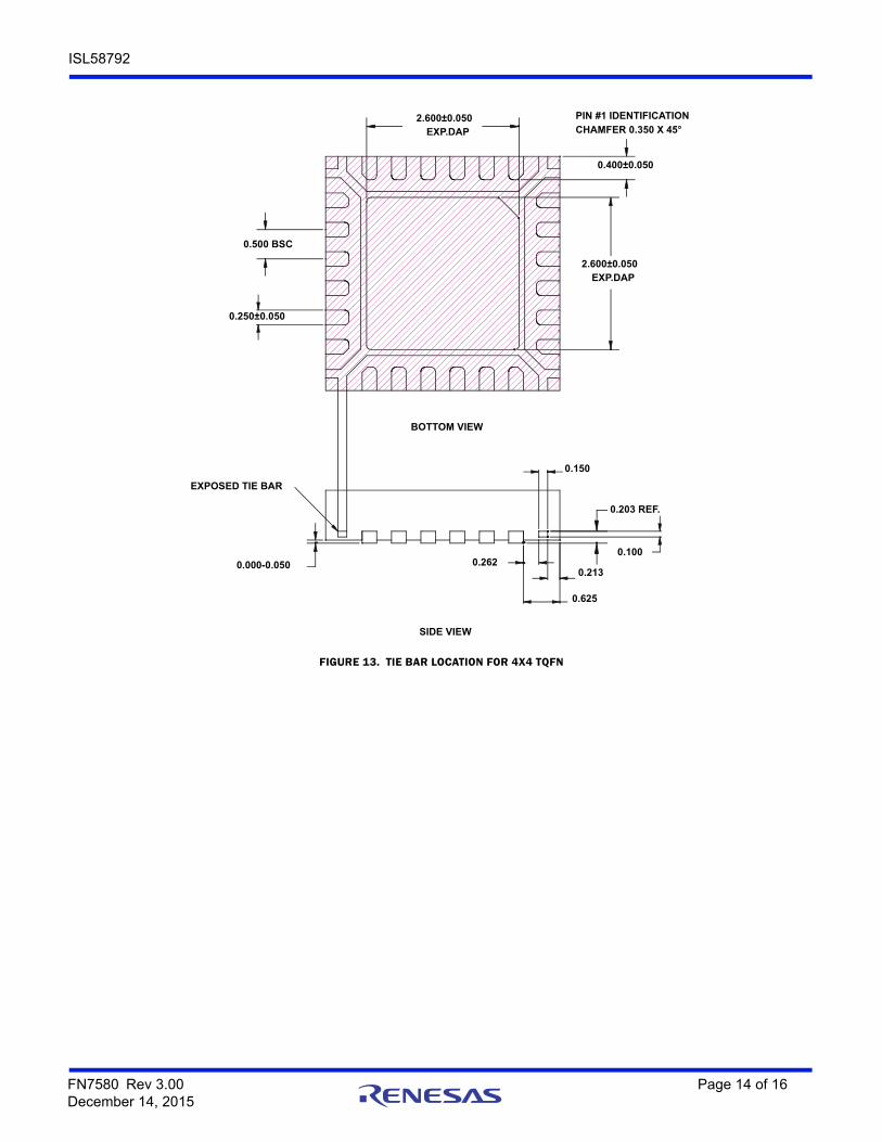
FIGURE 13. TIE BAR LOCATION FOR 4X4 TQFN
0.000-0.050
0.203 REF.
0.2620.213
0.100
0.625
0.150
SIDE VIEW
BOTTOM VIEW
PIN #1 IDENTIFICATION
CHAMFER 0.350 X 45°2.600±0.050
EXP.DAP
2.600±0.050EXP.DAP
0.500 BSC
0.400±0.050
0.250±0.050
EXPOSED TIE BAR
FN7580 Rev 3.00 Page 14 of 16December 14, 2015
ISL58792
Intersil products are manufactured, assembled and tested utilizing ISO9001 quality systems as notedin the quality certifications found at www.intersil.com/en/support/qualandreliability.html
Intersil products are sold by description only. Intersil may modify the circuit design and/or specifications of products at any time without notice, provided that such modification does not, in Intersil's sole judgment, affect the form, fit or function of the product. Accordingly, the reader is cautioned to verify that datasheets are current before placing orders. Information furnished by Intersil is believed to be accurate and reliable. However, no responsibility is assumed by Intersil or its subsidiaries for its use; nor for any infringements of patents or other rights of third parties which may result from its use. No license is granted by implication or otherwise under any patent or patent rights of Intersil or its subsidiaries.
For information regarding Intersil Corporation and its products, see www.intersil.com
For additional products, see www.intersil.com/en/products.html
© Copyright Intersil Americas LLC 2010-2015. All Rights Reserved.All trademarks and registered trademarks are the property of their respective owners.
About IntersilIntersil Corporation is a leading provider of innovative power management and precision analog solutions. The company's products address some of the largest markets within the industrial and infrastructure, mobile computing and high-end consumer markets.
For the most updated datasheet, application notes, related documentation and related parts, please see the respective product information page found at www.intersil.com.
You may report errors or suggestions for improving this datasheet by visiting www.intersil.com/ask.
Reliability reports are also available from our website at www.intersil.com/support.
Revision HistoryThe revision history provided is for informational purposes only and is believed to be accurate, but not warranted. Please go to web to make sure you have the latest Rev.
DATE REVISION CHANGE
December 14, 2015 FN7580.3 Removed ISL58792CRTZ-EVAL from Ordering Information table.Updated POD L24.4x4E from rev 0 to rev 2. Changes since rev 2:- Bottom View - Changed Exposed paddle dimension from 2.50 to 2.60- Made correction in Typical land pattern - added 0 to .250- Added tolerance to Exposed DAP in Bottom view:From: 2.60 sq.To: 2.60 ±0.10 with added square graphic in front of the 2.60
July 29, 2013 FN7580.2 Updated Products information verbiage to About Intersil verbiage.
January 6, 2012 FN7580.1 Added ISL58792CRTZ and ISL58792CRTZ-T7A to “Ordering Information” on page 3.
November 29, 2010 FN7580.0 Initial release.
FN7580 Rev 3.00 Page 15 of 16December 14, 2015
ISL58792
FN7580 Rev 3.00 Page 16 of 16December 14, 2015
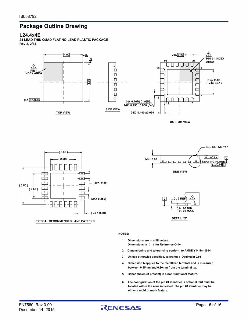
Package Outline Drawing
L24.4x4E24 LEAD THIN QUAD FLAT NO-LEAD PLASTIC PACKAGERev 2, 2/14
TYPICAL RECOMMENDED LAND PATTERNDETAIL "X"
SIDE VIEW
TOP VIEW
BOTTOM VIEW
located within the zone indicated. The pin #1 identifier may be
Unless otherwise specified, tolerance : Decimal ± 0.05
Tiebar shown (if present) is a non-functional feature.
The configuration of the pin #1 identifier is optional, but must be
between 0.15mm and 0.30mm from the terminal tip.
Dimension b applies to the metallized terminal and is measured
Dimensions in ( ) for Reference Only.
Dimensioning and tolerancing conform to AMSE Y14.5m-1994.
6.
either a mold or mark feature.
3.
5.
4.
2.
Dimensions are in millimeters.1.
NOTES:
C 0 . 2 REF
0 . 05 MAX.0 . 00 MIN.
5
4.00 A
B
4.00
(4X) 0.15
6PIN 1
INDEX AREA
19PIN #1 INDEX
24
20X 0.50
Exp. DAP
6
118
12
24X 0.400 ±0.050
7
6
Max 0.80
SEE DETAIL "X"
SEATING PLANE0.08
0.10 CC
C
( 3.80 )( 2.60 )
( 24 X 0.60)
(24X 0.250)
( 20X 0.50)
( 3.80 )
( 2.60)
0.1024X 0.250 ±0.050
AM C B4
SIDE VIEW
2.60 ±0.10
13
AREA