Embed Size (px)
Citation preview
FN8162Rev 5.00
July 5, 2016
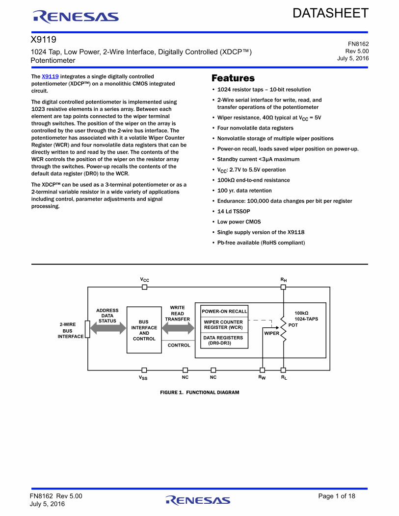
X91191024 Tap, Low Power, 2-Wire Interface, Digitally Controlled (XDCP™) Potentiometer
DATASHEET
The X9119 integrates a single digitally controlled potentiometer (XDCP™) on a monolithic CMOS integrated circuit.
The digital controlled potentiometer is implemented using 1023 resistive elements in a series array. Between each element are tap points connected to the wiper terminal through switches. The position of the wiper on the array is controlled by the user through the 2-wire bus interface. The potentiometer has associated with it a volatile Wiper Counter Register (WCR) and four nonvolatile data registers that can be directly written to and read by the user. The contents of the WCR controls the position of the wiper on the resistor array through the switches. Power-up recalls the contents of the default data register (DR0) to the WCR.
The XDCP™ can be used as a 3-terminal potentiometer or as a 2-terminal variable resistor in a wide variety of applications including control, parameter adjustments and signal processing.
Features• 1024 resistor taps – 10-bit resolution
• 2-Wire serial interface for write, read, and transfer operations of the potentiometer
• Wiper resistance, 40Ω typical at VCC = 5V
• Four nonvolatile data registers
• Nonvolatile storage of multiple wiper positions
• Power-on recall, loads saved wiper position on power-up.
• Standby current <3µA maximum
• VCC: 2.7V to 5.5V operation
• 100kΩ end-to-end resistance
• 100 yr. data retention
• Endurance: 100,000 data changes per bit per register
• 14 Ld TSSOP
• Low power CMOS
• Single supply version of the X9118
• Pb-free available (RoHS compliant)
FIGURE 1. FUNCTIONAL DIAGRAM
RH
RL
BUS
RW
INTERFACE
CONTROL
POT
VCC
VSS
2-WIRE
BUS
ADDRESSDATA
STATUS
WRITEREAD
WIPER
1024-TAPSTRANSFER
NC NC
100kΩPOWER-ON RECALL
WIPER COUNTERREGISTER (WCR)
DATA REGISTERS(DR0-DR3)CONTROL
INTERFACEAND
FN8162 Rev 5.00 Page 1 of 18July 5, 2016
X9119
ApplicationsCircuit Level• Vary the gain of a voltage amplifier
• Provide programmable DC reference voltages for comparators and detectors
• Control the volume in audio circuits
• Trim out the offset voltage error in a voltage amplifier circuit
• Set the output voltage of a voltage regulator
• Trim the resistance in Wheatstone bridge circuits
• Control the gain, characteristic frequency and Q-factor in filter circuits
• Set the scale factor and zero point in sensor signal conditioning circuits
• Vary the frequency and duty cycle of timer ICs
• Vary the DC biasing of a pin diode attenuator in RF circuits
• Provide a control variable (I, V, or R) in feedback circuits
System Level• Adjust the contrast in LCD displays
• Control the power level of LED transmitters in communication systems
• Set and regulate the DC biasing point in an RF power amplifier in wireless systems
• Control the gain in audio and home entertainment systems
• Provide the variable DC bias for tuners in RF wireless systems
• Set the operating points in temperature control systems
• Control the operating point for sensors in industrial systems
• Trim offset and gain errors in artificial intelligent systems
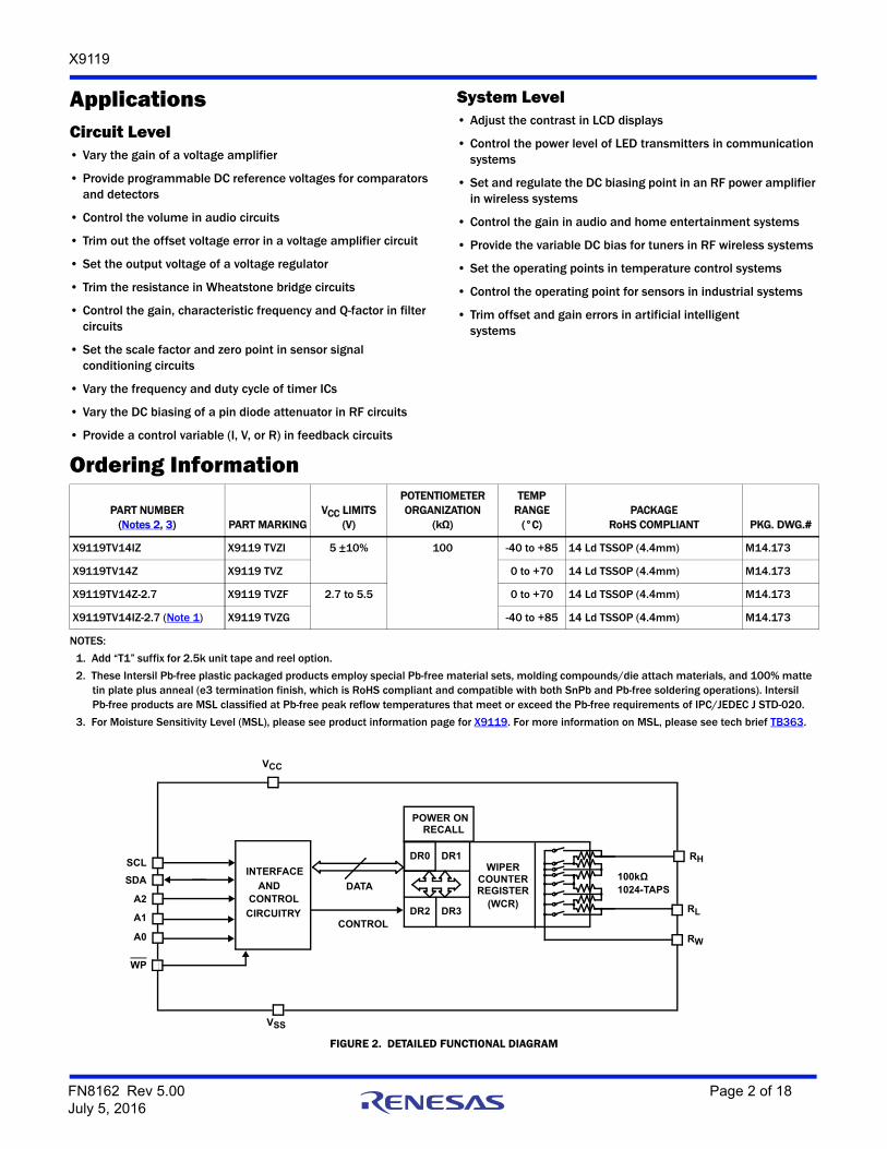
Ordering Information
PART NUMBER(Notes 2, 3) PART MARKING
VCC LIMITS (V)
POTENTIOMETER ORGANIZATION
(kΩ)
TEMP RANGE
(°C)PACKAGE
RoHS COMPLIANT PKG. DWG.#
X9119TV14IZ X9119 TVZI 5 ±10% 100 -40 to +85 14 Ld TSSOP (4.4mm) M14.173
X9119TV14Z X9119 TVZ 0 to +70 14 Ld TSSOP (4.4mm) M14.173
X9119TV14Z-2.7 X9119 TVZF 2.7 to 5.5 0 to +70 14 Ld TSSOP (4.4mm) M14.173
X9119TV14IZ-2.7 (Note 1) X9119 TVZG -40 to +85 14 Ld TSSOP (4.4mm) M14.173
NOTES:
1. Add “T1” suffix for 2.5k unit tape and reel option.
2. These Intersil Pb-free plastic packaged products employ special Pb-free material sets, molding compounds/die attach materials, and 100% matte tin plate plus anneal (e3 termination finish, which is RoHS compliant and compatible with both SnPb and Pb-free soldering operations). Intersil Pb-free products are MSL classified at Pb-free peak reflow temperatures that meet or exceed the Pb-free requirements of IPC/JEDEC J STD-020.
3. For Moisture Sensitivity Level (MSL), please see product information page for X9119. For more information on MSL, please see tech brief TB363.
FIGURE 2. DETAILED FUNCTIONAL DIAGRAM
SCL
A1
SDA
A2
WP
INTERFACE
ANDCONTROL
CIRCUITRY
VCC
VSS
DR0 DR1
DR2 DR3
WIPERCOUNTERREGISTER
(WCR)
RH
RL
DATA
RW
1024-TAPS100kΩ
CONTROL
POWER ON RECALL
A0
FN8162 Rev 5.00 Page 2 of 18July 5, 2016
X9119
Bus Interface Pins
SERIAL DATA INPUT/OUTPUT (SDA)The SDA is a bidirectional serial data input/output pin for a 2-wire slave device and is used to transfer data into and out of the device. It receives device address, opcode, wiper register address and data sent from a 2-wire master at the rising edge of the serial clock SCL, and it shifts out data after each falling edge of the serial clock SCL.
It is an open-drain output and may be wire-ORed with any number of open-drain or open collector outputs. An open-drain output requires the use of a pull-up resistor. For selecting typical values, refer to the guidelines for calculating typical values on the bus pull-up resistors graph.
SERIAL CLOCK (SCL)This input is used by a 2-wire master to supply a 2-wire serial clock to the X9119.
DEVICE ADDRESS (A2–A0)The Address inputs are used to set the least significant 3 bits of the 8-bit slave address. A match in the slave address serial data stream must be made with the Address input in order to initiate communication with the X9119. A maximum of 8 devices may occupy the 2-wire serial bus.
HARDWARE WRITE PROTECT INPUT (WP)The WP pin when LOW, prevents nonvolatile writes to the Data Registers.
Potentiometer Pins RH, RL The RH and RL pins are equivalent to the terminal connections on a mechanical potentiometer.
RWThe wiper pin are equivalent to the wiper terminal of a mechanical potentiometer.
Bias Supply Pins
SYSTEM SUPPLY VOLTAGE (VCC) AND SUPPLY GROUND (VSS)The VCC pin is the system supply voltage. The VSS pin is the system ground.
Other Pins
NO CONNECTNo connect pins should be left open. These pins are used for Intersil manufacturing and testing purposes.
Principals of OperationThe X9119 is an integrated microcircuit incorporating a resistor array and its associated registers and counters and the serial interface logic providing direct communication between the host and the digitally controlled potentiometer. This section provides detail description of the following:
• Resistor Array Description
• Serial Interface Description
• Instruction and Register Description
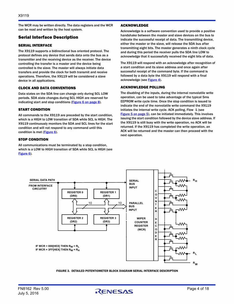
Resistor Array DescriptionThe X9119 is comprised of a resistor array. The array contains, in effect, 1023 discrete resistive segments that are connected in series (Figure 3 on page 4). The physical ends of each array are equivalent to the fixed terminals of a mechanical potentiometer (RH and RL inputs).
At both ends of each array and between each resistor segment is a CMOS switch connected to the wiper (RW) output. Within each individual array only one switch may be turned on at a time. These switches are controlled by the Wiper Counter Register (WCR). The 10-bits of the WCR (WCR[9:0]) are decoded to select, and enable, one of 1024 switches.
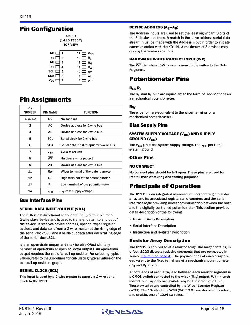
Pin ConfigurationX9119
(14 LD TSSOP)TOP VIEW
Pin AssignmentsPIN
NUMBER PIN NAME FUNCTION
1, 3, 10 NC No connect
2 A0 Device address for 2-wire bus
4 A2 Device address for 2-wire bus
5 SCL Serial clock for 2-wire bus
6 SDA Serial data input/output for 2-wire bus
7 VSS System ground
8 WP Hardware write protect
9 A1 Device address for 2-wire bus
11 RW Wiper terminal of the potentiometer
12 RH High terminal of the potentiometer
13 RL Low terminal of the potentiometer
14 VCC System supply voltage
VCC
RL
VSS
1
2
3
4
5
6
7 8
14
13
12
11
10
9
NC
RWA2
A1
RH
A0
NC
SDANCSCL
WP
FN8162 Rev 5.00 Page 3 of 18July 5, 2016
X9119
The WCR may be written directly. The data registers and the WCR can be read and written by the host system.
Serial Interface Description
SERIAL INTERFACEThe X9119 supports a bidirectional bus oriented protocol. The protocol defines any device that sends data onto the bus as a transmitter and the receiving device as the receiver. The device controlling the transfer is a master and the device being controlled is the slave. The master will always initiate data transfers and provide the clock for both transmit and receive operations. Therefore, the X9119 will be considered a slave device in all applications.
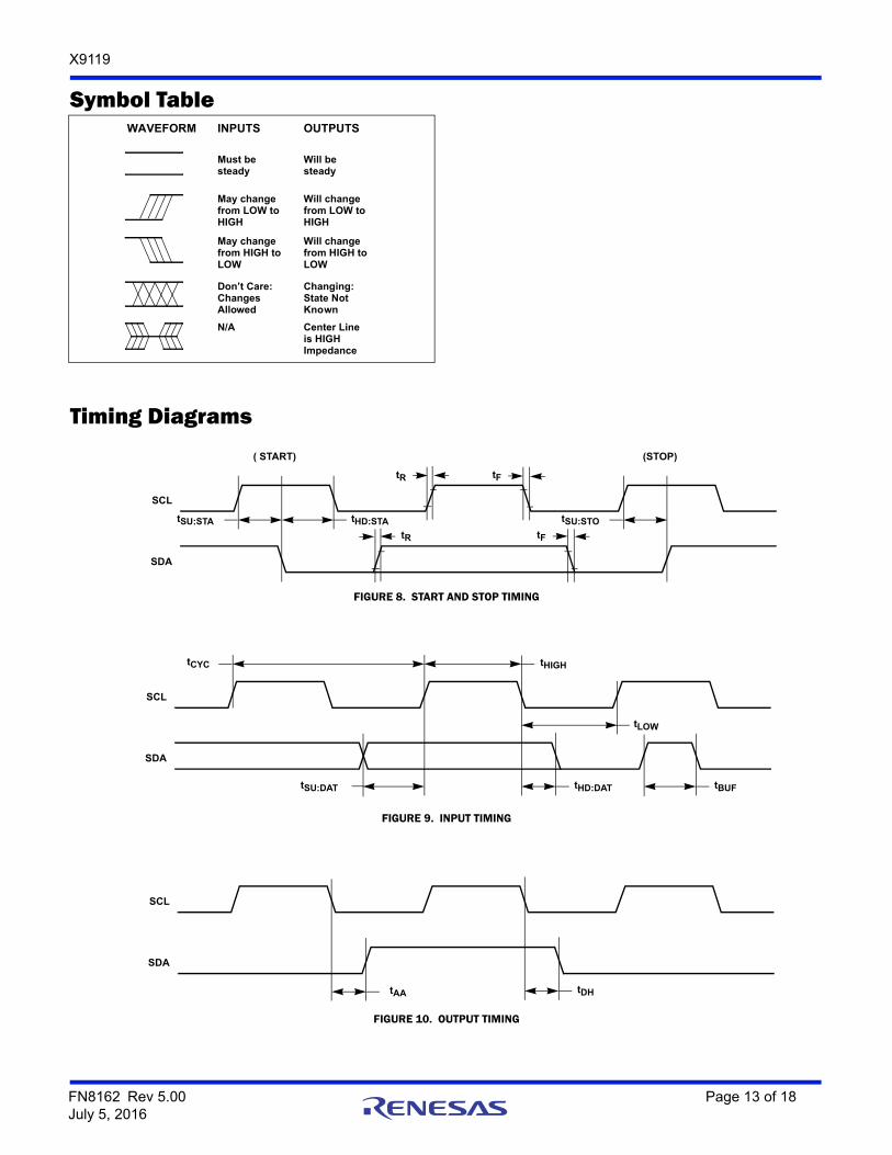
CLOCK AND DATA CONVENTIONSData states on the SDA line can change only during SCL LOW periods. SDA state changes during SCL HIGH are reserved for indicating start and stop conditions (Figure 6 on page 8).
START CONDITIONAll commands to the X9119 are preceded by the start condition, which is a HIGH to LOW transition of SDA while SCL is HIGH. The X9119 continuously monitors the SDA and SCL lines for the start condition and will not respond to any command until this condition is met (Figure 6).
STOP CONDITIONAll communications must be terminated by a stop condition, which is a LOW to HIGH transition of SDA while SCL is HIGH (see Figure 6).
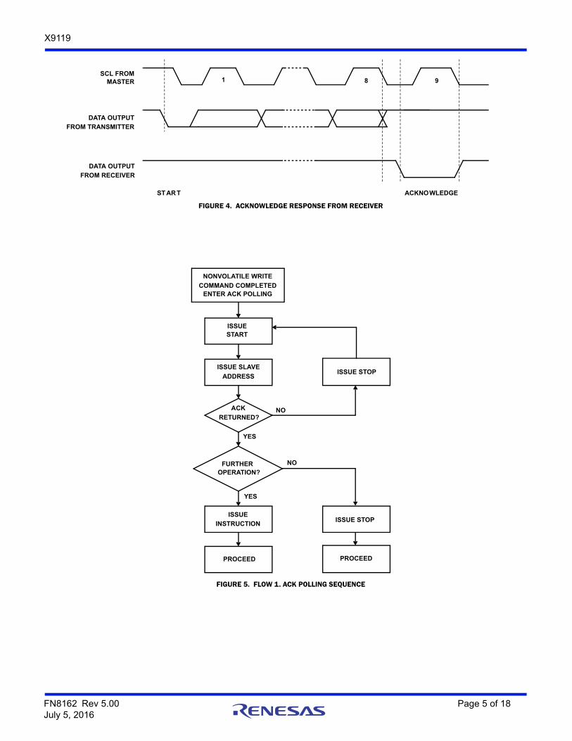
ACKNOWLEDGEAcknowledge is a software convention used to provide a positive handshake between the master and slave devices on the bus to indicate the successful receipt of data. The transmitting device, either the master or the slave, will release the SDA bus after transmitting eight bits. The master generates a ninth clock cycle and during this period the receiver pulls the SDA line LOW to acknowledge that it successfully received the eight bits of data.
The X9119 will respond with an acknowledge after recognition of a start condition and its slave address and once again after successful receipt of the command byte. If the command is followed by a data byte the X9119 will respond with a final acknowledge (see Figure 4).
ACKNOWLEDGE POLLINGThe disabling of the inputs, during the internal nonvolatile write operation, can be used to take advantage of the typical 5ms EEPROM write cycle time. Once the stop condition is issued to indicate the end of the nonvolatile write command the X9119 initiates the internal write cycle. ACK polling, Flow 1 (see Figure 5 on page 5), can be initiated immediately. This involves issuing the start condition followed by the device slave address. If the X9119 is still busy with the write operation, no ACK will be returned. If the X9119 has completed the write operation, an ACK will be returned and the master can then proceed with the next operation.
FIGURE 3. DETAILED POTENTIOMETER BLOCK DIAGRAM SERIAL INTERFACE DESCRIPTION
SERIAL DATA PATH
FROM INTERFACE
REGISTER 0
SERIALBUSINPUT
PARALLELBUSINPUT
COUNTERREGISTER
RH
RL
RW
10 10
COUNTER
DECODE
WIPER
(WCR)
(DR0)
CIRCUITRYREGISTER 1
(DR1)
REGISTER 2(DR2)
REGISTER 3(DR3)
R
IF WCR = 000[HEX] THEN RW = RLIF WCR = 3FF[HEX] THEN RW = RH
FN8162 Rev 5.00 Page 4 of 18July 5, 2016
X9119
FIGURE 4. ACKNOWLEDGE RESPONSE FROM RECEIVER
FIGURE 5. FLOW 1. ACK POLLING SEQUENCE
SCL FROMMASTER
DATA OUTPUT
FROM TRANSMITTER
1 8 9
ST AR T ACKNOWLEDGE
DATA OUTPUT
FROM RECEIVER
NONVOLATILE WRITE
COMMAND COMPLETEDENTER ACK POLLING
ISSUESTART
ISSUE SLAVE
ADDRESS
ACK
RETURNED?
FURTHEROPERATION?
ISSUE
INSTRUCTIONISSUE STOP
NO
YES
YES
PROCEED
ISSUE STOP
NO
PROCEED
FN8162 Rev 5.00 Page 5 of 18July 5, 2016
X9119
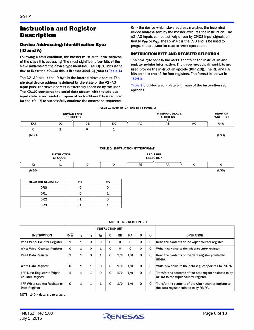
Instruction and Register DescriptionDevice Addressing: Identification Byte (ID and A) Following a start condition, the master must output the address of the slave it is accessing. The most significant four bits of the slave address are the device type identifier. The ID[3:0] bits is the device ID for the X9119; this is fixed as 0101[B] (refer to Table 1).
The A2–A0 bits in the ID byte is the internal slave address. The physical device address is defined by the state of the A2–A0 input pins. The slave address is externally specified by the user. The X9119 compares the serial data stream with the address input state; a successful compare of both address bits is required for the X9119 to successfully continue the command sequence.
Only the device which slave address matches the incoming device address sent by the master executes the instruction. The A2–A0 inputs can be actively driven by CMOS input signals or tied to VCC or VSS. The R/W bit is the LSB and is be used to program the device for read or write operations.
INSTRUCTION BYTE AND REGISTER SELECTIONThe next byte sent to the X9119 contains the instruction and register pointer information. The three most significant bits are used provide the instruction opcode (IOP[2:0]). The RB and RA bits point to one of the four registers. The format is shown in Table 2.
Table 3 provides a complete summary of the instruction set opcodes.
TABLE 1. IDENTIFICATION BYTE FORMAT
TABLE 2. INSTRUCTION BYTE FORMAT
ID3 ID2 ID1 ID0 A2 A1 A0 R/W
0 1 0 1
(MSB) (LSB)
DEVICE TYPEIDENTIFIES
INTERNAL SLAVEADDRESS
READ ORWRITE BIT
I2 I1 I0 0 RB RA 0 0
(MSB) (LSB)
INSTRUCTIONOPCODE
REGISTERSELECTION
REGISTER SELECTED RB RA
DR0 0 0
DR1 0 1
DR2 1 0
DR3 1 1
TABLE 3. INSTRUCTION SET
INSTRUCTION
INSTRUCTION SET
OPERATIONR/W I2 I1 I0 0 RB RA 0 0
Read Wiper Counter Register 1 1 0 0 0 0 0 0 0 Read the contents of the wiper counter register.
Write Wiper Counter Register 0 1 0 1 0 0 0 0 0 Write new value to the wiper counter register.
Read Data Register 1 1 0 1 0 1/0 1/0 0 0 Read the contents of the data register pointed to RB-RA.
Write Data Register 0 1 1 0 0 1/0 1/0 0 0 Write new value to the data register pointed to RB-RA.
XFR Data Register to Wiper Counter Register
1 1 1 0 0 1/0 1/0 0 0 Transfer the contents of the data register pointed to by RB-RA to the wiper counter register.
XFR Wiper Counter Register to Data Register
0 1 1 1 0 1/0 1/0 0 0 Transfer the contents of the wiper counter register to the data register pointed to by RB-RA.
NOTE: 1/0 = data is one or zero.
FN8162 Rev 5.00 Page 6 of 18July 5, 2016
X9119
Instruction and Register DescriptionDevice Addressing
WIPER COUNTER REGISTER (WCR)The X9119 contains a wiper counter register (refer to Table 4) for the XDCP potentiometer. The WCR is equivalent to a serial-in, parallel-out register/counter with its outputs decoded to select one of 1024 switches along its resistor array. The contents of the WCR can be altered in one of three ways:
1. It may be written directly by the host via the write wiper counter register instruction (serial load).
2. It may be written indirectly by transferring the contents of one of four associated data registers via the XFR data register.
3. It is loaded with the contents of its data register zero (R0) upon power-up.
The wiper counter register is a volatile register; that is, its contents are lost when the X9119 is powered-down. Although the register is automatically loaded with the value in DR0 upon power-up, this may be different from the value present at power-down. Power-up guidelines are recommended to ensure proper loadings of the DR0 value into the WCR.
DATA REGISTERS (DR0 TO DR3)The potentiometer has four 10-bit nonvolatile data registers. These can be read or written directly by the host. Data can also be transferred between any of the four data registers and the wiper counter register. All operations changing data in one of the data registers is a nonvolatile operation and will take a maximum of 10ms.
If the application does not require storage of multiple settings for the potentiometer, the Data Registers can be used as regular memory locations for system parameters or user preference data.
Bit 9 to Bit 0 are used to store one of the 1024 wiper position (0 ~1023).
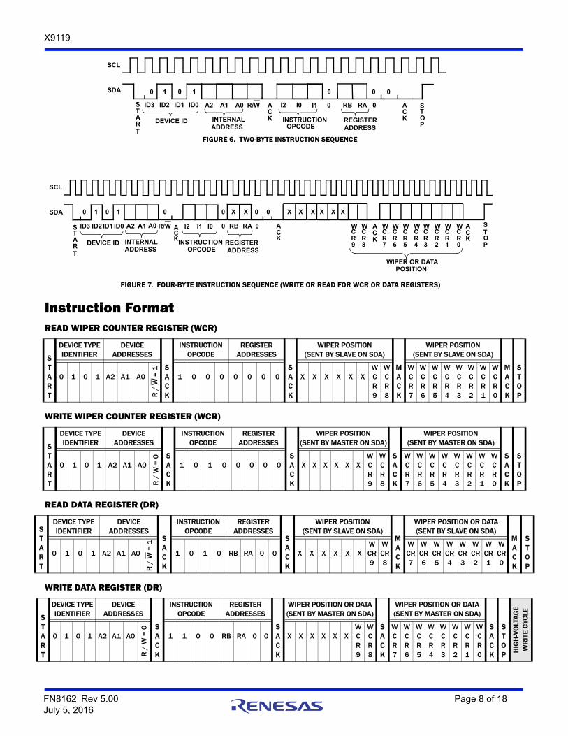
Four of the six instructions are four bytes in length. These instructions are:
• Read Wiper Counter Register – Reads the current wiper position of the selected potentiometer.
• Write Wiper Counter Register – Changes current wiper position of the selected potentiometer.
• Read Data Register – Reads the contents of the selected Data Register.
• Write Data Register – Writes a new value to the selected Data Register.
The basic sequence of the four byte instructions is illustrated in Figure 6 on page 8. These 4-byte instructions exchange data between the WCR and one of the data registers. A transfer from a data register to a WCR is essentially a write to a static RAM, with the static RAM controlling the wiper position. The response of the wiper to this action will be delayed by tWRL. A transfer from the WCR (current wiper position), to a data register is a write-to-nonvolatile memory and takes a minimum of tWR to complete. The transfer can occur between one of the four potentiometers and one of its associated registers.
Two instructions (Figure 7 on page 8) require a 2-byte sequence to complete. These instructions transfer data between the host and the X9119; either between the host and one of the data registers or directly between the host and the wiper counter register. These instructions are:
• XFR Data Register to Wiper Counter Register – This transfers the contents of one specified data register to the wiper counter register.
• XFR Wiper Counter Register to Data Register – This transfers the contents of the wiper counter register to the specified data register.
See “Instruction Format” on page 8 for more details.
POWER-UP AND POWER-DOWN REQUIREMENTSThere are no restrictions on the power-up condition of VCC and the voltages applied to the potentiometer pins provided that the VCC is always more positive than or equal to the voltages at RH, RL, and RW, i.e., VCC ≥ RH, RL, RW. There are no restrictions on the power-down condition. However, the datasheet parameters for the DCP do not apply until 1ms after VCC reaches its final value.
TABLE 4. WIPER CONTROL REGISTER, WCR (10-BIT), WCR9–WCR0: USED TO STORE THE CURRENT WIPER POSITION (VOLATILE, V)
WCR9 WCR8 WCR7 WCR6 WCR5 WCR4 WCR3 WCR2 WCR1 WCR0
V V V V V V V V V V
(MSB) (LSB)
TABLE 5. DATA REGISTER, DR (10-BIT), BIT 9–BIT 0: USED TO STORE WIPER POSITIONS OR DATA (NONVOLATILE, NV)
BIT 9 BIT 8 BIT 7 BIT 6 BIT 5 BIT 4 BIT 3 BIT 2 BIT 1 BIT 0
NV NV NV NV NV NV NV NV NV NV
MSB LSB
FN8162 Rev 5.00 Page 7 of 18July 5, 2016
X9119
Instruction FormatREAD WIPER COUNTER REGISTER (WCR)
WRITE WIPER COUNTER REGISTER (WCR)
READ DATA REGISTER (DR)
WRITE DATA REGISTER (DR)
START
0 1 0 1
A2 A1 A0 R/W ACK
I2 I1I0 0 RB RA 0 ACK
SCL
SDA
STOP
0 0 0
ID3 ID2 ID1 ID0
DEVICE ID INTERNAL INSTRUCTIONOPCODEADDRESS
REGISTERADDRESS
FIGURE 6. TWO-BYTE INSTRUCTION SEQUENCE
START
ACK
ACK
SCL
SDA
ACK
STOP
ACK
ID3 ID2 ID1 ID0 A2 A1 A0 R/W I2 0
0 0 X X 0 0 X X X
WCR9
WCR4
WCR3
WCR2
WCR1
WCR0
I1 I0 0 RB RA
0 1 0 1 X X X
DEVICE ID INTERNAL ADDRESS
INSTRUCTIONOPCODE
REGISTERADDRESS
WIPER OR DATAPOSITION
FIGURE 7. FOUR-BYTE INSTRUCTION SEQUENCE (WRITE OR READ FOR WCR OR DATA REGISTERS)
WCR8
WCR7
WCR6
WCR5
START
DEVICE TYPEIDENTIFIER
DEVICEADDRESSES
SACK
INSTRUCTIONOPCODE
REGISTERADDRESSES
SACK
WIPER POSITION(SENT BY SLAVE ON SDA)
MACK
WIPER POSITION(SENT BY SLAVE ON SDA)
MACK
STOP
0 1 0 1 A2 A1 A0
R /
W =
1
1 0 0 0 0 0 0 0 X X X X X XWCR9
WCR8
WCR7
WCR6
WCR5
WCR4
WCR3
WCR2
WCR1
WCR0
START
DEVICE TYPEIDENTIFIER
DEVICEADDRESSES
SACK
INSTRUCTIONOPCODE
REGISTERADDRESSES
SACK
WIPER POSITION (SENT BY MASTER ON SDA)
SACK
WIPER POSITION(SENT BY MASTER ON SDA)
SACK
STOP
0 1 0 1 A2 A1 A0
R /
W =
0
1 0 1 0 0 0 0 0 X X X X X XWCR9
WCR8
WCR7
WCR6
WCR5
WCR4
WCR3
WCR2
WCR1
WCR0
START
DEVICE TYPEIDENTIFIER
DEVICEADDRESSES
SACK
INSTRUCTIONOPCODE
REGISTERADDRESSES
SACK
WIPER POSITION(SENT BY SLAVE ON SDA)
MACK
WIPER POSITION OR DATA(SENT BY SLAVE ON SDA)
MACK
STOP
0 1 0 1 A2 A1 A0
R /
W =
1
1 0 1 0 RB RA 0 0 X X X X X XWCR9
WCR8
WCR7
WCR6
WCR5
WCR4
WCR3
WCR2
WCR1
WCR0
START
DEVICE TYPEIDENTIFIER
DEVICEADDRESSES
SACK
INSTRUCTIONOPCODE
REGISTERADDRESSES
SACK
WIPER POSITION OR DATA(SENT BY MASTER ON SDA)
SACK
WIPER POSITION OR DATA(SENT BY MASTER ON SDA)
SACK
STOP H
IGH
-VO
LTA
GE
WR
ITE
CYC
LE
0 1 0 1 A2 A1 A0
R /
W =
0
1 1 0 0 RB RA 0 0 X X X X X XWCR9
WCR8
WCR7
WCR6
WCR5
WCR4
WCR3
WCR2
WCR1
WCR0
FN8162 Rev 5.00 Page 8 of 18July 5, 2016
X9119
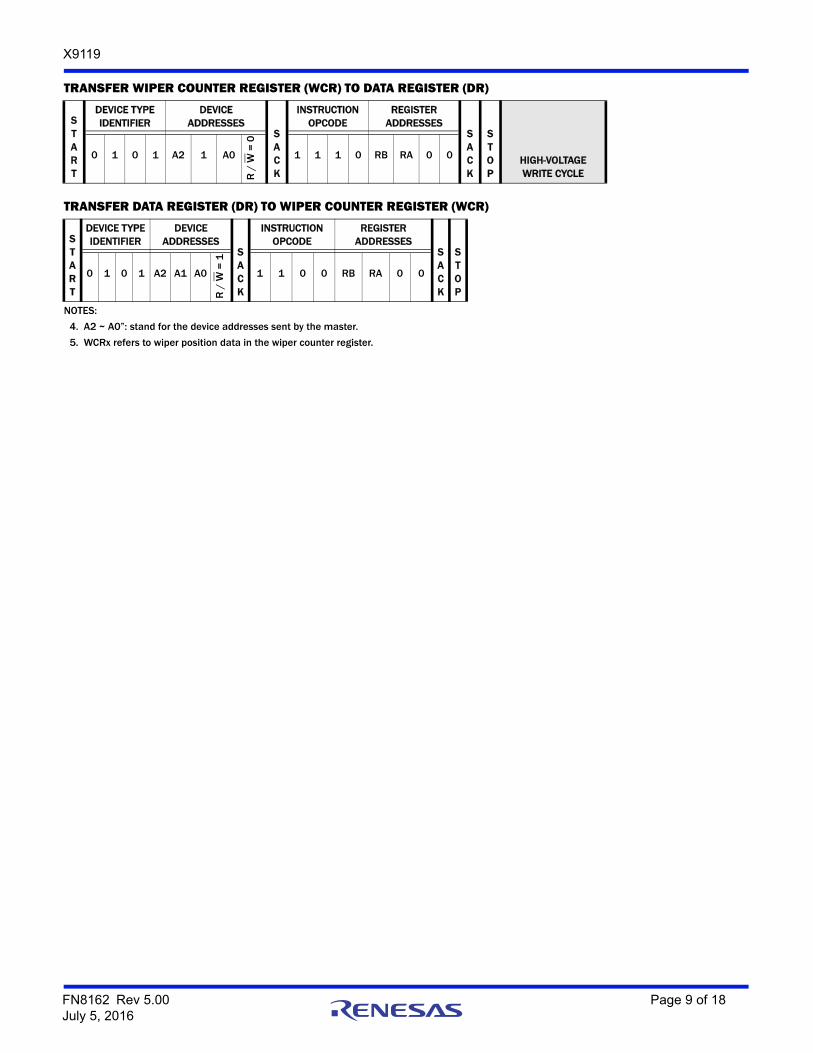
TRANSFER WIPER COUNTER REGISTER (WCR) TO DATA REGISTER (DR)
TRANSFER DATA REGISTER (DR) TO WIPER COUNTER REGISTER (WCR)
START
DEVICE TYPEIDENTIFIER
DEVICEADDRESSES
SACK
INSTRUCTIONOPCODE
REGISTERADDRESSES
SACK
STOP
HIGH-VOLTAGEWRITE CYCLE
0 1 0 1 A2 1 A0
R /
W =
0
1 1 1 0 RB RA 0 0
START
DEVICE TYPEIDENTIFIER
DEVICEADDRESSES
SACK
INSTRUCTIONOPCODE
REGISTERADDRESSES
SACK
STOP
0 1 0 1 A2 A1 A0
R /
W =
1
1 1 0 0 RB RA 0 0
NOTES:
4. A2 ~ A0”: stand for the device addresses sent by the master.
5. WCRx refers to wiper position data in the wiper counter register.
FN8162 Rev 5.00 Page 9 of 18July 5, 2016
X9119
Absolute Maximum Ratings Voltage on SCL, SDA, or any address input with respect to VSS . . . . . . . . . . . . . . . . . . . . . . . . . . . . . . . . . . . . . . -1V to +7VV = | (VH–VL) | . . . . . . . . . . . . . . . . . . . . . . . . . . . . . . . . . . . . . . . . . . . . . . 5VIW (10s) . . . . . . . . . . . . . . . . . . . . . . . . . . . . . . . . . . . . . . . . . . . . . . . . . . ±6mA
Operating ConditionsCommercial . . . . . . . . . . . . . . . . . . . . . . . . . . . . . . . . . . . . . . . . 0°C to +70°CIndustrial . . . . . . . . . . . . . . . . . . . . . . . . . . . . . . . . . . . . . . . . . -40° to +85°CSupply Voltage (VCC) Limits (Note 9)
X9119 . . . . . . . . . . . . . . . . . . . . . . . . . . . . . . . . . . . . . . . . . . . . . . .5V ±10%X9119-2.7 . . . . . . . . . . . . . . . . . . . . . . . . . . . . . . . . . . . . . . . . . 2.7V to 5.5V
Thermal InformationTemperature under bias . . . . . . . . . . . . . . . . . . . . . . . . . . .-65°C to +135°CStorage temperature . . . . . . . . . . . . . . . . . . . . . . . . . . . . . .-65°C to +150°CLead temperature (soldering, 10s). . . . . . . . . . . . . . . . . . . . . . . . . . . .300°CPb-Free Reflow Profile . . . . . . . . . . . . . . . . . . . . . . . . . . . . . . . . . . see TB493
CAUTION: Do not operate at or near the maximum ratings listed for extended periods of time. Exposure to such conditions may adversely impact productreliability and result in failures not covered by warranty.
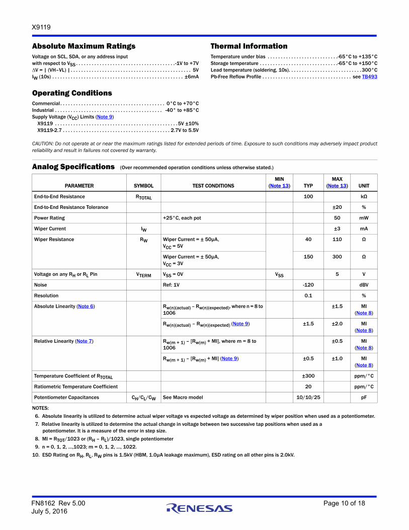
Analog Specifications (Over recommended operation conditions unless otherwise stated.)
PARAMETER SYMBOL TEST CONDITIONSMIN
(Note 13) TYPMAX
(Note 13) UNIT
End-to-End Resistance RTOTAL 100 kΩ
End-to-End Resistance Tolerance ±20 %
Power Rating +25°C, each pot 50 mW
Wiper Current IW ±3 mA
Wiper Resistance RW Wiper Current = ± 50µA, VCC = 5V
40 110 Ω
Wiper Current = ± 50µA, VCC = 3V
150 300 Ω
Voltage on any RH or RL Pin VTERM VSS = 0V VSS 5 V
Noise Ref: 1V -120 dBV
Resolution 0.1 %
Absolute Linearity (Note 6) Rw(n)(actual) – Rw(n)(expected), where n = 8 to 1006
±1.5 MI(Note 8)
Rw(n)(actual) – Rw(n)(expected) (Note 9) ±1.5 ±2.0 MI(Note 8)
Relative Linearity (Note 7) Rw(m + 1) – [Rw(m) + MI], where m = 8 to 1006
±0.5 MI(Note 8)
Rw(m + 1) – [Rw(m) + MI] (Note 9) ±0.5 ±1.0 MI(Note 8)
Temperature Coefficient of RTOTAL ±300 ppm/°C
Ratiometric Temperature Coefficient 20 ppm/°C
Potentiometer Capacitances CH/CL/CW See Macro model 10/10/25 pF
NOTES:
6. Absolute linearity is utilized to determine actual wiper voltage vs expected voltage as determined by wiper position when used as a potentiometer.
7. Relative linearity is utilized to determine the actual change in voltage between two successive tap positions when used as a potentiometer. It is a measure of the error in step size.
8. MI = RTOT/1023 or (RH – RL)/1023, single potentiometer
9. n = 0, 1, 2, …,1023; m = 0, 1, 2, …, 1022.
10. ESD Rating on RH, RL, RW pins is 1.5kV (HBM, 1.0µA leakage maximum), ESD rating on all other pins is 2.0kV.
FN8162 Rev 5.00 Page 10 of 18July 5, 2016
X9119
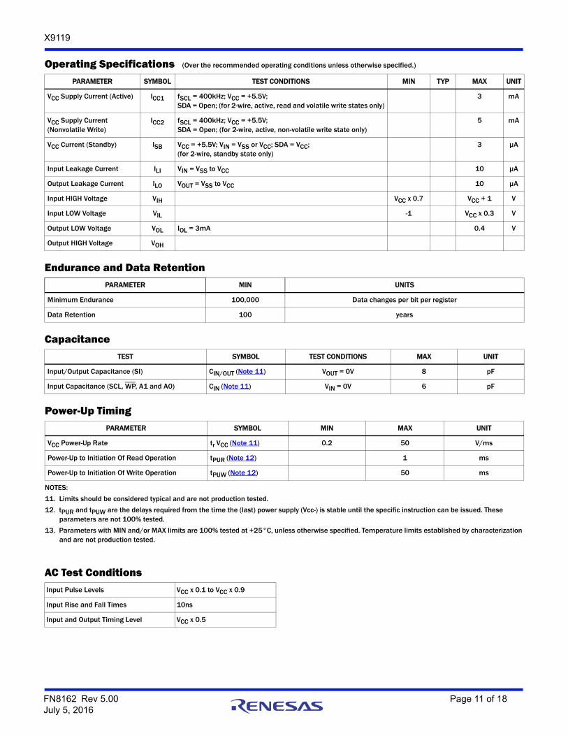
Operating Specifications (Over the recommended operating conditions unless otherwise specified.)
PARAMETER SYMBOL TEST CONDITIONS MIN TYP MAX UNIT
VCC Supply Current (Active) ICC1 fSCL = 400kHz; VCC = +5.5V;SDA = Open; (for 2-wire, active, read and volatile write states only)
3 mA
VCC Supply Current (Nonvolatile Write)
ICC2 fSCL = 400kHz; VCC = +5.5V;SDA = Open; (for 2-wire, active, non-volatile write state only)
5 mA
VCC Current (Standby) ISB VCC = +5.5V; VIN = VSS or VCC; SDA = VCC;(for 2-wire, standby state only)
3 µA
Input Leakage Current ILI VIN = VSS to VCC 10 µA
Output Leakage Current ILO VOUT = VSS to VCC 10 µA
Input HIGH Voltage VIH VCC x 0.7 VCC + 1 V
Input LOW Voltage VIL -1 VCC x 0.3 V
Output LOW Voltage VOL IOL = 3mA 0.4 V
Output HIGH Voltage VOH
Endurance and Data RetentionPARAMETER MIN UNITS
Minimum Endurance 100,000 Data changes per bit per register
Data Retention 100 years
CapacitanceTEST SYMBOL TEST CONDITIONS MAX UNIT
Input/Output Capacitance (SI) CIN/OUT (Note 11) VOUT = 0V 8 pF
Input Capacitance (SCL, WP, A1 and A0) CIN (Note 11) VIN = 0V 6 pF
Power-Up TimingPARAMETER SYMBOL MIN MAX UNIT
VCC Power-Up Rate tr VCC (Note 11) 0.2 50 V/ms
Power-Up to Initiation Of Read Operation tPUR (Note 12) 1 ms
Power-Up to Initiation Of Write Operation tPUW (Note 12) 50 ms
NOTES:
11. Limits should be considered typical and are not production tested.
12. tPUR and tPUW are the delays required from the time the (last) power supply (Vcc-) is stable until the specific instruction can be issued. These parameters are not 100% tested.
13. Parameters with MIN and/or MAX limits are 100% tested at +25°C, unless otherwise specified. Temperature limits established by characterization and are not production tested.
AC Test ConditionsInput Pulse Levels VCC x 0.1 to VCC x 0.9
Input Rise and Fall Times 10ns
Input and Output Timing Level VCC x 0.5
FN8162 Rev 5.00 Page 11 of 18July 5, 2016
X9119
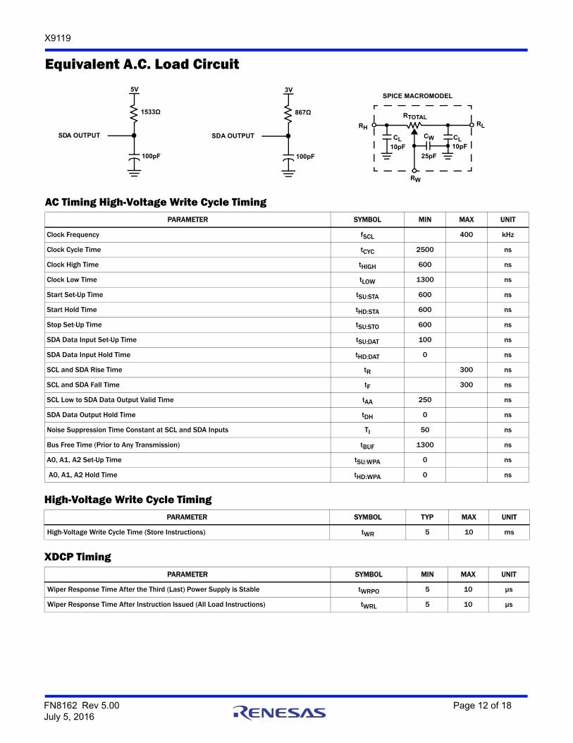
Equivalent A.C. Load Circuit
RH
10pF
CL CL
RW
RTOTAL
CW
25pF
10pF
RL
SPICE MACROMODEL5V
1533Ω
100pF
SDA OUTPUT
3V
867Ω
100pF
SDA OUTPUT
AC Timing High-Voltage Write Cycle TimingPARAMETER SYMBOL MIN MAX UNIT
Clock Frequency fSCL 400 kHz
Clock Cycle Time tCYC 2500 ns
Clock High Time tHIGH 600 ns
Clock Low Time tLOW 1300 ns
Start Set-Up Time tSU:STA 600 ns
Start Hold Time tHD:STA 600 ns
Stop Set-Up Time tSU:STO 600 ns
SDA Data Input Set-Up Time tSU:DAT 100 ns
SDA Data Input Hold Time tHD:DAT 0 ns
SCL and SDA Rise Time tR 300 ns
SCL and SDA Fall Time tF 300 ns
SCL Low to SDA Data Output Valid Time tAA 250 ns
SDA Data Output Hold Time tDH 0 ns
Noise Suppression Time Constant at SCL and SDA Inputs TI 50 ns
Bus Free Time (Prior to Any Transmission) tBUF 1300 ns
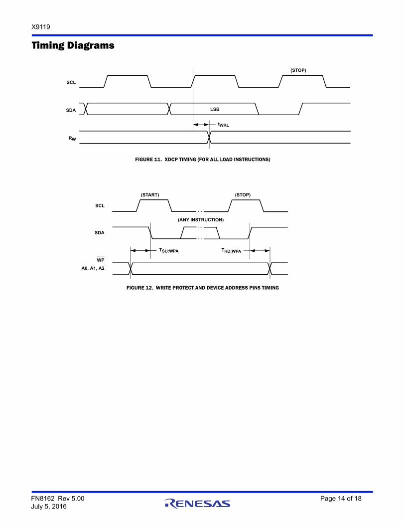
A0, A1, A2 Set-Up Time tSU:WPA 0 ns
A0, A1, A2 Hold Time tHD:WPA 0 ns
High-Voltage Write Cycle TimingPARAMETER SYMBOL TYP MAX UNIT
High-Voltage Write Cycle Time (Store Instructions) tWR 5 10 ms
XDCP TimingPARAMETER SYMBOL MIN MAX UNIT
Wiper Response Time After the Third (Last) Power Supply is Stable tWRPO 5 10 µs
Wiper Response Time After Instruction Issued (All Load Instructions) tWRL 5 10 µs
FN8162 Rev 5.00 Page 12 of 18July 5, 2016
X9119
Symbol TableWAVEFORM INPUTS OUTPUTS
Must besteady
Will besteady
May changefrom LOW to HIGH
Will changefrom LOW toHIGH
May changefrom HIGH toLOW
Will changefrom HIGH toLOW
Don’t Care:ChangesAllowed
Changing:State NotKnown
N/A Center Lineis HIGHImpedance
Timing Diagrams
FIGURE 8. START AND STOP TIMING
FIGURE 9. INPUT TIMING
FIGURE 10. OUTPUT TIMING
tSU:STA tHD:STA tSU:STO
SCL
SDA
tR
( START) (STOP)
tF
tR tF
SCL
SDA
tHIGH
tLOW
tCYC
tHD:DATtSU:DAT tBUF
SCL
SDA
tDHtAA
FN8162 Rev 5.00 Page 13 of 18July 5, 2016
X9119
FIGURE 11. XDCP TIMING (FOR ALL LOAD INSTRUCTIONS)
FIGURE 12. WRITE PROTECT AND DEVICE ADDRESS PINS TIMING
Timing Diagrams
SCL
SDA
RW
(STOP)
LSB
tWRL
SDA
SCL...
...
...
WP
A0, A1, A2
TSU:WPA THD:WPA
(START) (STOP)
(ANY INSTRUCTION)
FN8162 Rev 5.00 Page 14 of 18July 5, 2016
X9119
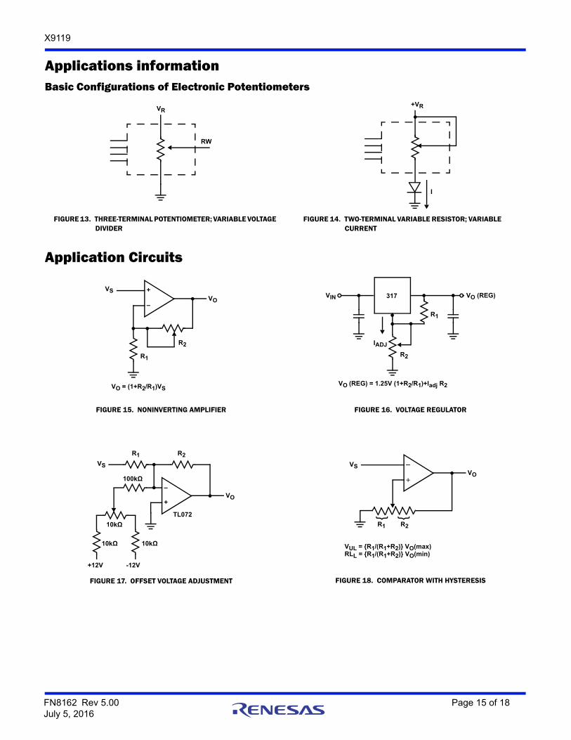
Applications informationBasic Configurations of Electronic Potentiometers
FIGURE 13. THREE-TERMINAL POTENTIOMETER; VARIABLE VOLTAGE DIVIDER
FIGURE 14. TWO-TERMINAL VARIABLE RESISTOR; VARIABLE CURRENT
VR
RW
+VR
I
Application Circuits
FIGURE 15. NONINVERTING AMPLIFIER FIGURE 16. VOLTAGE REGULATOR
FIGURE 17. OFFSET VOLTAGE ADJUSTMENT FIGURE 18. COMPARATOR WITH HYSTERESIS
+
–
VSVO
R2
R1
VO = (1+R2/R1)VS
R1
R2
IADJ
VO (REG) = 1.25V (1+R2/R1)+Iadj R2
VO (REG)VIN 317
+
–
VS
VO
R2R1
100kΩ
10kΩ10kΩ
10kΩ
-12V+12V
TL072
VUL = {R1/(R1+R2)} VO(max)RLL = {R1/(R1+R2)} VO(min)
+
–VSVO
R2R1
}}
FN8162 Rev 5.00 Page 15 of 18July 5, 2016
X9119
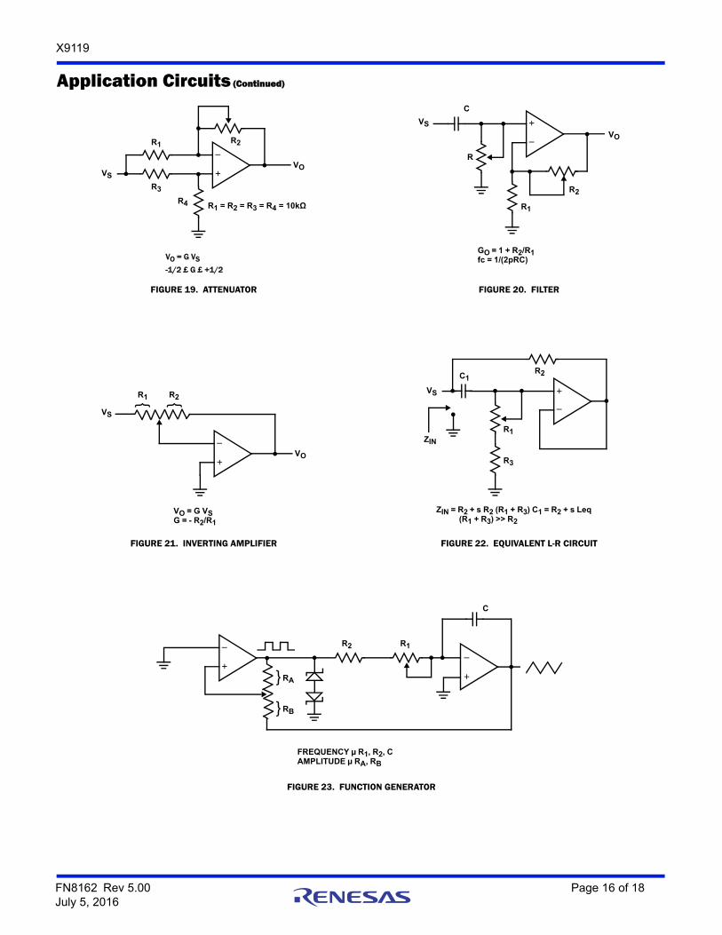
FIGURE 19. ATTENUATOR FIGURE 20. FILTER
FIGURE 21. INVERTING AMPLIFIER FIGURE 22. EQUIVALENT L-R CIRCUIT
FIGURE 23. FUNCTION GENERATOR
Application Circuits (Continued)
+
–
VSVO
R3
R1
VO = G VS
-1/2 £ G £ +1/2
R2
R4 R1 = R2 = R3 = R4 = 10kΩ
GO = 1 + R2/R1fc = 1/(2pRC)
+
–
VS
R2
R1
R
C
VO
+
–
VS
VO
R2R1 }}
VO = G VSG = - R2/R1
ZIN = R2 + s R2 (R1 + R3) C1 = R2 + s Leq (R1 + R3) >> R2
+
–
VS
R2C1
R1
R3
ZIN
+
– R2
+
–
R1
}
}
RA
RB
FREQUENCY µ R1, R2, CAMPLITUDE µ RA, RB
C
FN8162 Rev 5.00 Page 16 of 18July 5, 2016
X9119
Intersil products are manufactured, assembled and tested utilizing ISO9001 quality systems as notedin the quality certifications found at www.intersil.com/en/support/qualandreliability.html
Intersil products are sold by description only. Intersil may modify the circuit design and/or specifications of products at any time without notice, provided that such modification does not, in Intersil's sole judgment, affect the form, fit or function of the product. Accordingly, the reader is cautioned to verify that datasheets are current before placing orders. Information furnished by Intersil is believed to be accurate and reliable. However, no responsibility is assumed by Intersil or its subsidiaries for its use; nor for any infringements of patents or other rights of third parties which may result from its use. No license is granted by implication or otherwise under any patent or patent rights of Intersil or its subsidiaries.
For information regarding Intersil Corporation and its products, see www.intersil.com
For additional products, see www.intersil.com/en/products.html
© Copyright Intersil Americas LLC 2005-2016. All Rights Reserved.All trademarks and registered trademarks are the property of their respective owners.
About IntersilIntersil Corporation is a leading provider of innovative power management and precision analog solutions. The company's products address some of the largest markets within the industrial and infrastructure, mobile computing and high-end consumer markets.
For the most updated datasheet, application notes, related documentation and related parts, please see the respective product information page found at www.intersil.com.
You may report errors or suggestions for improving this datasheet by visiting www.intersil.com/ask.
Reliability reports are also available from our website at www.intersil.com/support.
Revision History The revision history provided is for informational purposes only and is believed to be accurate, but not warranted. Please go to the web to make sure that you have the latest revision.
DATE REVISION CHANGE
July 5, 2016 FN8162.5 Updated entire datasheet applying Intersil’s new standards.Updated title.Updated Ordering Information table by removing obsolete parts, updating Note 1 and adding Note 3.Removed Lead temperature (soldering, 10s) from the Thermal Information section on page 10.Updated Absolute Linearity maximum specification from “±1” to “±1.5”.Added Revision History and About Intersil sections.Updated POD to the latest revision changes are as follows:
Updated drawing to remove table and added land pattern.
FN8162 Rev 5.00 Page 17 of 18July 5, 2016
X9119
FN8162 Rev 5.00 Page 18 of 18July 5, 2016
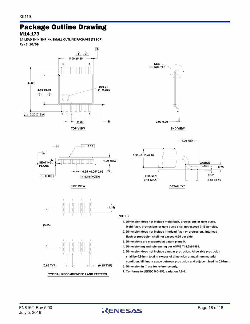
Package Outline DrawingM14.17314 LEAD THIN SHRINK SMALL OUTLINE PACKAGE (TSSOP)
Rev 3, 10/09
DETAIL "X"SIDE VIEW
TYPICAL RECOMMENDED LAND PATTERN
TOP VIEW
B
A
1 7
814
C
PLANESEATING
0.10 C 0.10 CBA
H
PIN #1I.D. MARK
5.00 ±0.10
4.40 ±0.10
0.25 +0.05/-0.06
6.40
0.20 C B A
0.05
0°-8°
GAUGEPLANE
SEE
0.90 +0.15/-0.10
0.60 ±0.15
0.09-0.20
5
2
31
3
1.00 REF
0.65
1.20 MAX
0.25
0.05 MIN0.15 MAX
(1.45)
(5.65)
(0.65 TYP) (0.35 TYP)
DETAIL "X"
1. Dimension does not include mold flash, protrusions or gate burrs.
Mold flash, protrusions or gate burrs shall not exceed 0.15 per side.
2. Dimension does not include interlead flash or protrusion. Interlead
flash or protrusion shall not exceed 0.25 per side.
3. Dimensions are measured at datum plane H.
4. Dimensioning and tolerancing per ASME Y14.5M-1994.
5. Dimension does not include dambar protrusion. Allowable protrusion
shall be 0.80mm total in excess of dimension at maximum material
condition. Minimum space between protrusion and adjacent lead is 0.07mm.
6. Dimension in ( ) are for reference only.
7. Conforms to JEDEC MO-153, variation AB-1.
NOTES:
END VIEW