Embed Size (px)
Citation preview
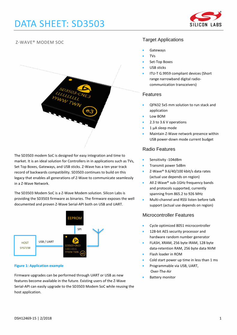
DATA SHEET: SD3503
DSH12469-15 | 2/2018 1
Z-WAVE® MODEM SOC
The SD3503 modem SoC is designed for easy integration and time to market. It is an ideal solution for Controllers in in applications such as TVs, Set Top Boxes, Gateways, and USB sticks. Z-Wave has a ten year track record of backwards compatibility. SD3503 continues to build on this legacy that enables all generations of Z-Wave to communicate seamlessly in a Z-Wave Network.
The SD3503 Modem SoC is a Z-Wave Modem solution. Silicon Labs is providing the SD3503 firmware as binaries. The firmware exposes the well documented and proven Z-Wave Serial-API both on USB and UART.
Figure 1: Application example
Firmware upgrades can be performed through UART or USB as new features become available in the future. Existing users of the Z-Wave Serial-API can easily upgrade to the SD3503 Modem SoC while reusing the host application.
USB / UART
SPI
EEPROM
Target Applications
• Gateways • TVs • Set-Top Boxes • USB sticks • ITU-T G.9959 compliant devices (Short
range narrowband digital radio-communication transceivers)
Features
• QFN32 5x5 mm solution to run stack and application
• Low BOM • 2.3 to 3.6 V operations • 1 µA sleep mode • Maintain Z-Wave network presence within
USB power-down mode current budget
Radio Features
• Sensitivity -104dBm • Transmit power 5dBm • Z-Wave® 9.6/40/100 kbit/s data rates
(actual use depends on region) • All Z-Wave® sub-1GHz frequency bands
and protocols supported, currently spanning from 865.2 to 926 MHz
• Multi-channel and RSSI listen before talk support (actual use depends on region)
Microcontroller Features
• Cycle optimized 8051 microcontroller • 128-bit AES security processor and
hardware random number generator • FLASH, XRAM, 256 byte IRAM, 128 byte
data-retention RAM, 256 byte data NVM • Flash loader in ROM • Cold start power up time in less than 1 ms • Programmable via USB, UART,
Over-The-Air • Battery monitor
Datasheet: SD3503
2 DSH12469-15 | 2/2018
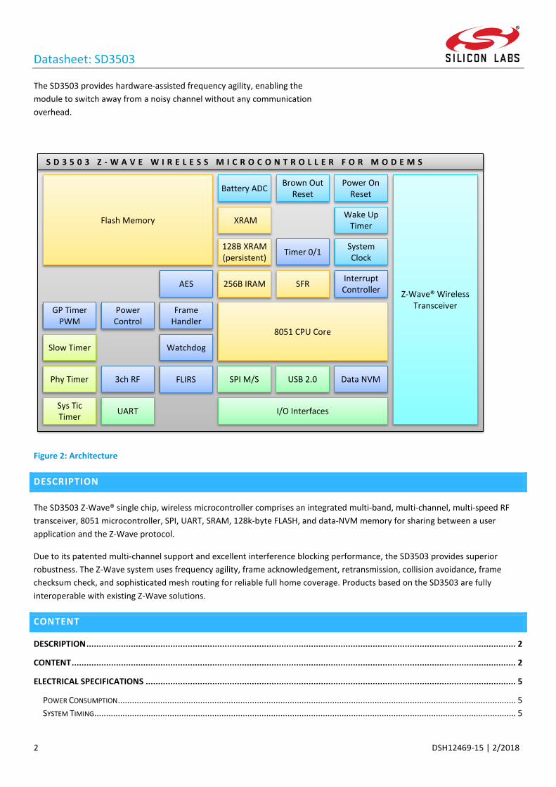
The SD3503 provides hardware-assisted frequency agility, enabling the module to switch away from a noisy channel without any communication overhead.
Figure 2: Architecture
DESCRIPTION
The SD3503 Z-Wave® single chip, wireless microcontroller comprises an integrated multi-band, multi-channel, multi-speed RF transceiver, 8051 microcontroller, SPI, UART, SRAM, 128k-byte FLASH, and data-NVM memory for sharing between a user application and the Z-Wave protocol.
Due to its patented multi-channel support and excellent interference blocking performance, the SD3503 provides superior robustness. The Z-Wave system uses frequency agility, frame acknowledgement, retransmission, collision avoidance, frame checksum check, and sophisticated mesh routing for reliable full home coverage. Products based on the SD3503 are fully interoperable with existing Z-Wave solutions.
CONTENT
DESCRIPTION .............................................................................................................................................................................. 2
CONTENT .................................................................................................................................................................................... 2
ELECTRICAL SPECIFICATIONS ...................................................................................................................................................... 5
POWER CONSUMPTION ......................................................................................................................................................................... 5 SYSTEM TIMING ................................................................................................................................................................................... 5
S D 3 5 0 3 Z - W A V E W I R E L E S S M I C R O C O N T R O L L E R F O R M O D E M S
AES
GP Timer PWM
Power Control
Frame Handler
Slow Timer Watchdog
Phy Timer 3ch RF FLIRS
Sys Tic Timer UART I/O Interfaces
SPI M/S USB 2.0
Z-Wave® Wireless Transceiver
Data NVM
8051 CPU Core
256B IRAM SFR Interrupt Controller
Flash Memory
128B XRAM (persistent) Timer 0/1 System
Clock
XRAM Wake Up Timer
Battery ADC Brown Out Reset
Power On Reset

Datasheet: SD3503
DSH12469-15 | 2/2018 3
NON-VOLATILE MEMORIES ..................................................................................................................................................................... 6 RF TRANSCEIVER CHARACTERISTICS ......................................................................................................................................................... 6 DIGITAL IO CHARACTERISTICS ................................................................................................................................................................. 7
3.3V systems ............................................................................................................................................................................... 7 Sub 3V systems ............................................................................................................................................................................ 8 Typical IO characteristics, VDD= 2.3V to 3.6V, TA = -40 to +90°C .................................................................................................. 8
BATTERY-ADC CHARACTERISTICS ............................................................................................................................................................ 9
ABSOLUTE MAXIMUM RATINGS ............................................................................................................................................... 10
PRODUCTION TEST CONDITIONS ........................................................................................................................................................... 10 QUALIFICATION TEST CONDITIONS ........................................................................................................................................................ 10
OVERVIEW ................................................................................................................................................................................ 11
WIRELESS TRANSCEIVER ........................................................................................................................................................... 12
INTERFACING THE FRONT-END .............................................................................................................................................................. 12 Z-WAVE FREQUENCY COVERAGE .......................................................................................................................................................... 12
CPU .......................................................................................................................................................................................... 13
MODES ............................................................................................................................................................................................ 13 Programming Mode .................................................................................................................................................................. 14
PERIPHERALS AND AUXILIARY BLOCKS ..................................................................................................................................... 14
SUPPLY SYSTEM ................................................................................................................................................................................. 14 XTAL AND SYSTEM CLOCK ................................................................................................................................................................... 15
Production considerations......................................................................................................................................................... 15 WAKE-UP-TIMER .............................................................................................................................................................................. 15 BATTERY MONITOR ADC .................................................................................................................................................................... 15 SPI ................................................................................................................................................................................................. 15 UART ............................................................................................................................................................................................. 16 USB ................................................................................................................................................................................................ 17
USB-Bus-Powered And Suspend-Mode Support ........................................................................................................................ 17 AES SECURITY PROCESSOR .................................................................................................................................................................. 17 RESET .............................................................................................................................................................................................. 17
PIN DESCRIPTIONS .................................................................................................................................................................... 18
PINS: 900 MHZ Z-WAVE RADIO .......................................................................................................................................................... 18 PINS: SYSTEM INTERFACE .................................................................................................................................................................... 18 PINS PER PIN NUMBER ......................................................................................................................................................................... 19
PROCESS SPECIFICATION .......................................................................................................................................................... 19
PCB MOUNTING AND SOLDERING ............................................................................................................................................ 20
RECOMMENDED PCB MOUNTING PATTERN ............................................................................................................................................ 20 SOLDERING INFORMATION ................................................................................................................................................................... 20
ORDERING INFORMATION ........................................................................................................................................................ 21
PACKAGE .................................................................................................................................................................................. 21
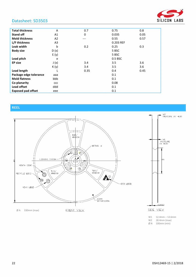
REEL ......................................................................................................................................................................................... 22
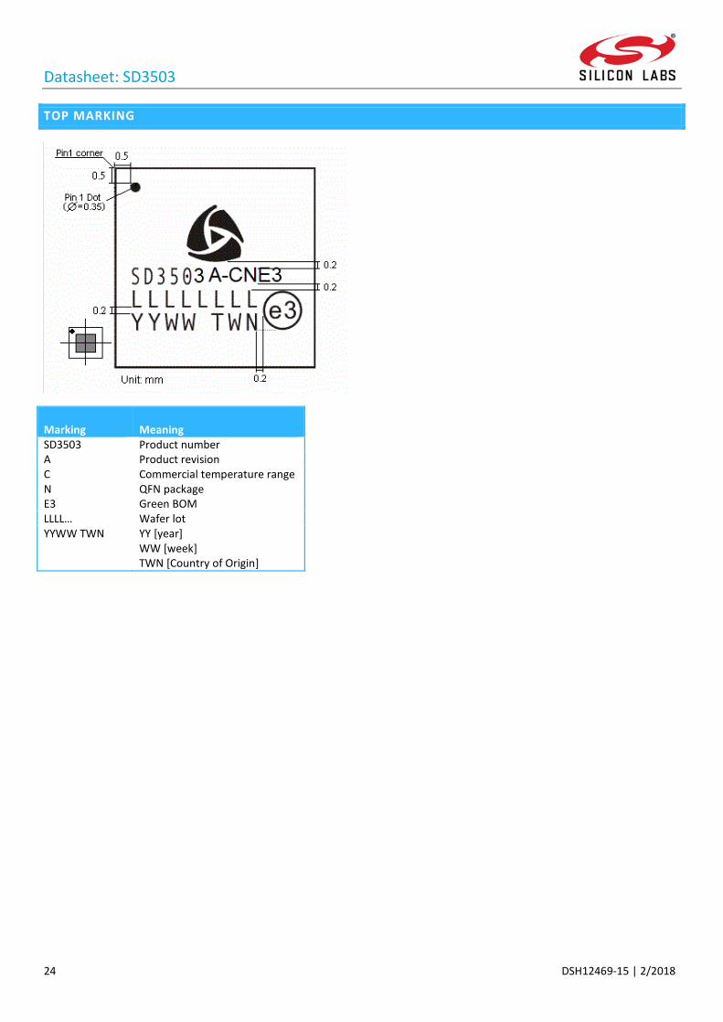
TOP MARKING .......................................................................................................................................................................... 24
Datasheet: SD3503
4 DSH12469-15 | 2/2018
DOCUMENT CHANGE LIST ........................................................................................................................................................ 25
Datasheet: SD3503
DSH12469-15 | 2/2018 5
ELECTRICAL SPECIFICATIONS
NOTES
For absolute Maximum Ratings, refer to page 10. For Qualification Test Conditions, TA = -40 to 90°C, VDD = 2.3 to 3.6V, refer to page 10. For Production Test Conditions, refer to page 10.
POWER CONSUMPTION
Supply Voltage Range TA = -40 to +90°C Min Max Units VDD Supply Voltage 2.3 3.6 V VDD USB Supply Voltage when the USB PHY is used 3.0 3.6 V VBOR The supply voltage at which the Brown Out Detector (BOR) resets the chip.
The BOR will reset the device if the supply is inadequate to guarantee correct behavior.
2.3 V
Power Saving Modes, VDD= 3.3V, TA = 25°C Typ Max Units IVDD SLEEP Interruptible sleep mode 1.0 1.6 µA ΔIVDD WUT Enabling Wake-up Timer in a sleep mode adds 0.7 µA ΔIVDD RAM Enabling SRAM data persistency in a sleep mode adds 0.1 µA IUSB SLEEP USB sleep mode with full data & state persistency & Wake-up Timer & system
clock 1.9 2.1 mA
Power Saving Modes, VDD = 3.0 to 3.6V, TA = -40 to +90°C Max Units IUSB SLEEP USB suspend mode with full data & state persistency & Wake-up Timer &
system clock 2.3 mA
Active Modes, VDD= 3.3V, TA = 25°C Typ Max Units IVDD MCU MCU running at 32MHz 15 16 mA IVDD MCU RX MCU and receiver (RX mode) 32 34 mA IVDD MCU TX 0.5 MCU and transmitter (TX mode), 0.5 dBm 34 36 mA IVDD MCU TX 3.5 MCU and transmitter (TX mode), 3.5 dBm 36 38 mA ΔIVDD ADC Using the ADC adds 0.15 0.25 mA ΔIVDD USB Using the USB adds mA Programming modes, VDD= 3.3V, TA = 25°C Typ Max Units IVDD PGM USB Programming via USB 15 mA IVDD PGM UART Programming via UART 15 16 mA
SYSTEM TIMING
System Start-Up Time, VDD = 2.3 to 3.6V, TA = -40 to +90°C Max Units TPOWER UP System Start-Up Time, measured from the supply voltage reach the minimum
VDD (=2.3V) and to the MCU responds, using qualification schematic and a power rise time not exceeding 10µs. Note 1: This value applies identically for recovery after brown-out events. Note 2: There is no restriction on the supply rise time. But an increase in power rise time will increase the Start-Up time proportionally.
1 ms
Datasheet: SD3503
6 DSH12469-15 | 2/2018
Wake-up Timer precision, VDD = 2.3 to 3.6V, TA = -40 to +90°C Max Units TWUT OFFSET Wake-up Timer accuracy, max offset deviation 40 ms TWUT SCALE Wake-up Timer accuracy, max scale deviation 2%
Reset and Interrupt timing requirements, VDD = 2.3 to 3.6V, TA = -40 to +90°C Max Units TRST_PULSE Minimum time RESET_N must be held down to guarantee a full system reset 20 ns TINT_PULSE To guarantee recognition of an external interrupt pulse, an input pin, if
configured to sample external interrupts, must be held down two complete clock cycles.
65 ns
NON-VOLATILE MEMORIES
Endurance and Retention Min Units FLASH (code) endurance 10k cycle Data NVM endurance 100k cycle FLASH Retention 100 year Data NVM Retention 100 year
The Flash and the NVM Data Array is built with SuperFlash® technology.
RF TRANSCEIVER CHARACTERISTICS
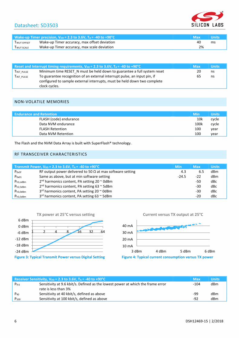
Transmit Power, VDD = 2.3 to 3.6V, TA = -40 to +90°C Min Max Units P0x3F RF output power delivered to 50 Ω at max software setting 4.3 6.5 dBm P0x01 Same as above, but at min software setting -24.5 -22 dBm Ph2,odBm 2nd harmonics content, PA setting 20 ~ 0dBm -50 dBc Ph2,5dBm 2nd harmonics content, PA setting 63 ~ 5dBm -30 dBc Ph3,0dBm 3rd harmonics content, PA setting 20 ~ 0dBm -30 dBc Ph3,5dBm 3rd harmonics content, PA setting 63 ~ 5dBm -20 dBc
Figure 3: Typical Transmit Power versus Digital Setting
Figure 4: Typical current consumption versus TX power
-24 dBm-18 dBm-12 dBm
-6 dBm0 dBm6 dBm
1 2 4 8 16 32 64
TX power at 25°C versus setting
10 mA
20 mA
30 mA
40 mA
3 dBm 4 dBm 5 dBm 6 dBm
Current versus TX output at 25°C
Receiver Sensitivity, VDD = 2.3 to 3.6V, TA = -40 to +90°C Max Units P9.6 Sensitivity at 9.6 kbit/s. Defined as the lowest power at which the frame error
rate is less than 3% -104 dBm
P40 Sensitivity at 40 kbit/s, defined as above -99 dBm P100 Sensitivity at 100 kbit/s, defined as above -92 dBm
Datasheet: SD3503
DSH12469-15 | 2/2018 7
Figure 5: Typical Sensitivity (average over process corners)
Figure 6: Typical Blocking performance
Blocking @40kbit/s, RSSI, LO leakage, intermodulation at VDD= 3.3V, TA = 25°C Typ Units PBLOCK 1MHz Blocking at Δf=1MHz. Blocker level is defined relative to a wanted signal and
measured with the wanted signal 3 dB above the sensitivity level 34 dBc
PBLOCK 2MHz Blocking at Δf=2MHz. Defined as above 38 dBc PBLOCK 5MHz Blocking at Δf=5MHz. Defined as above 60 dBc PBLOCK 10MHz Blocking at Δf=10MHz. Defined as above 63 dBc PBLOCK 100MHz Blocking at Δf=100MHz. Defined as above 68 dBc RSSIRANGE RSSI Dynamic Range 70 dB RSSILSB RSSI Resolution 1.5 dB PL LO leakage -80 dBm IIP3 Intermodulation distortion product, third order interception point -12 dBm
NOTES
1. All Z-Wave frequencies and modulation forms apply unless noted otherwise. Z-Wave frequencies currently span from 868.42MHz (EU) to 926MHz (Japan).
2. Crystal must be rated or calibrated to 32MHz ±25ppm. 3. Region specific impedance matching circuits according to reference designs applies. 4. Power level specifications are valid at the RF pin of the chip.
DIGITAL IO CHARACTERISTICS
IO pins have a nominal drive capability of 8mA (or 16mA) at the nominal 3.3V supply conditions. They are however fully functional down to 2.3V. Digital input pins, including all GPIO pins, features Schmitt trigger input hysteresis.
3.3V SYSTEMS Output Pins, VDD = 3.0V to 3.6V, TA = -40 to +90°C Min Max Units VOH High level output voltage, sourcing 8mA 2.4 V VOL Low level output voltage, sinking 8mA 0.4 V TRISE Rise Time, 10% to 90%, 2pF external load 10 ns TFALL Fall Time, 90% to 10%, 2pF external load 10 ns Input Pins, VDD = 3.0V to 3.6V, TA = -40 to +90°C Min Max Units VIF Falling input trigger threshold 0.9 1.3 V VIR Rising input trigger threshold 1.6 2.1 V ΔVI Hysteresis 0.65 0.95 V IIN Input current, 0V ≤ VIN ≤ VDD when internal pull-up is not available -10 10 µA IPULL UP Input current at VIN=0V when internal pull-up is available 40 120 µA CIN Input capacitance 10 pF
-110 dBm
-106 dBm
-102 dBm
-98 dBm
-94 dBm
-90 dBm
-40°C 20°C 80°C
Sens
itivi
ty 100 kb/s
40 kb/s
9.6 kb/s -10
20
50
80
-5 0 5
Pow
er (d
Bc)
Offset (MHz)
9.6
40
100
Datasheet: SD3503
8 DSH12469-15 | 2/2018
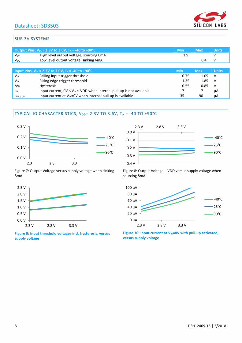
SUB 3V SYSTEMS Output Pins, VDD= 2.3V to 3.0V, TA = -40 to +90°C Min Max Units VOH High level output voltage, sourcing 6mA 1.9 V VOL Low level output voltage, sinking 6mA 0.4 V Input Pins, VDD= 2.3V to 3.0V, TA = -40 to +90°C Min Max Units VIF Falling input trigger threshold 0.75 1.05 V VIR Rising edge trigger threshold 1.35 1.85 V ΔVI Hysteresis 0.55 0.85 V IIN Input current, 0V ≤ VIN ≤ VDD when internal pull-up is not available -7 7 µA IPULL UP Input current at VIN=0V when internal pull-up is available 35 90 µA
TYPICAL IO CHARACTERISTICS, VDD= 2.3V TO 3.6V, TA = -40 TO +90°C
Figure 7: Output Voltage versus supply voltage when sinking 8mA
Figure 8: Output Voltage – VDD versus supply voltage when sourcing 8mA
Figure 9: Input threshold voltages incl. hysteresis, versus supply voltage
Figure 10: Input current at VIN=0V with pull-up activated, versus supply voltage
0.0 V
0.1 V
0.2 V
0.3 V
2.3 2.8 3.3
-40°C
25°C
90°C
-0.4 V
-0.3 V
-0.2 V
-0.1 V
0.0 V2.3 V 2.8 V 3.3 V
-40°C
25°C
90°C
0.0 V
0.5 V
1.0 V
1.5 V
2.0 V
2.5 V
2.3 V 2.8 V 3.3 V0 µA
20 µA
40 µA
60 µA
80 µA
100 µA
2.3 V 2.8 V 3.3 V
-40°C
25°C
90°C

Datasheet: SD3503
DSH12469-15 | 2/2018 9
Figure 11: Internal pull up current versus pin voltage, 25°C, VDD=3.3V and VDD=2.5V Pull up resistance ranges 17kΩ to 25kΩ at 25°C.
BATTERY-ADC CHARACTERISTICS
12 bit A to D converter, VDD = 2.3 to 3.6V, TA = -40 to +90°C Min Max Units VBG Internal Voltage Reference, referenced to GND 1.2 1.3 V Differential non-linearity -1 1 LSB Accuracy at sampling 10k samples per second at 12 bit resolution -5 5 LSB Accuracy at sampling 20k samples per second at 8 bit resolution -2 2 LSB
0 µA20 µA40 µA60 µA80 µA
100 µA
0 V 1 V 2 V 3 V 4 V
I pin 3.3V 17kΩ
I pin 2.5V 25kΩ
DATA SHEET: SD3503
DSH12469-15 | 2/2018 10
ABSOLUTE MAXIMUM RATINGS
Max Ratings Min Max Units VDD Supply voltage and other 3.3V rated pins as indicated in the Pin Descriptions
section, page 18 -0.3 3.6 V
VIO Voltage applied on output pins -0.3 5.5 V VCORE Voltage applied on low-voltage analogue pins and other 1.5 V rated pins as
indicated in the Pin Descriptions section, page 18 -0.3 1.8 V
PRF-IN RX input power 10 dBm TJ Operating Junction Temperature Range -55 125 °C TSTORAGE Storage temperature range -40 85 °C IVDD MAX Max total continuous supply consumption 120 mA VESD-HBM All pins tested according to JESD22-A114 JEDEC Human Body Model JESD22-
A114 2k V
VESD-CDM All pins tested according to JEDEC Charged Device Model JESD22-C101 500 V ILatchUp IO pins Latch-Up Test JESD78, current stress 100 mA VLatchUp Supply pins Latch-Up Test JESD78, voltage stress 5.4 V
NOTES
1. Stresses beyond those listed under “Max Ratings” may cause permanent damages to the device 2. These are stress ratings only. Functional operation of these devices beyond the ratings stated in the operational
sections of the specifications is not implied. 3. Exposure to absolute maximum rating conditions for extended periods may affect device reliability. 4. TX matching network design will influence TXVRF PEAK on TX output pin. 5. Caution: ESD sensitive device
PRODUCTION TEST CONDITIONS
The following conditions apply for the production final test unless noted otherwise.
1. Ambient temperature TA = 25°C 2. Supply voltage VDD = 3.3V 3. Crystal frequency = 32MHz 4. TX output power is measured at 900MHz 5. RX sensitivity is measured at 900.2MHz 6. All RF input and output levels referred to the pins of the chip (not the RF module). 7. Conditions include using production test schematic
QUALIFICATION TEST CONDITIONS
The following conditions apply for the qualification test unless noted otherwise.
1. Ambient temperature TA = -40 to +90°C. 2. Supply voltage VDD = 2.3 to 3.6V 3. Crystal frequency = 32MHz 4. RF performance measured across the span of Z-Wave frequencies 5. All RF input and output levels referred to the pins of the chip (not the RF module) 6. Conditions include using qualification test schematic 7. Conditions include using Z-Wave qualified RF drivers
Datasheet: SD3503
DSH12469-15 | 2/2018 11
OVERVIEW
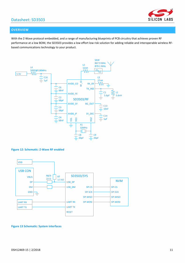
With the Z-Wave protocol embedded, and a range of manufacturing blueprints of PCB circuitry that achieves proven RF performance at a low BOM, the SD3503 provides a low effort low risk solution for adding reliable and interoperable wireless RF-based communications technology to your product.
Figure 12: Schematic: Z-Wave RF enabled
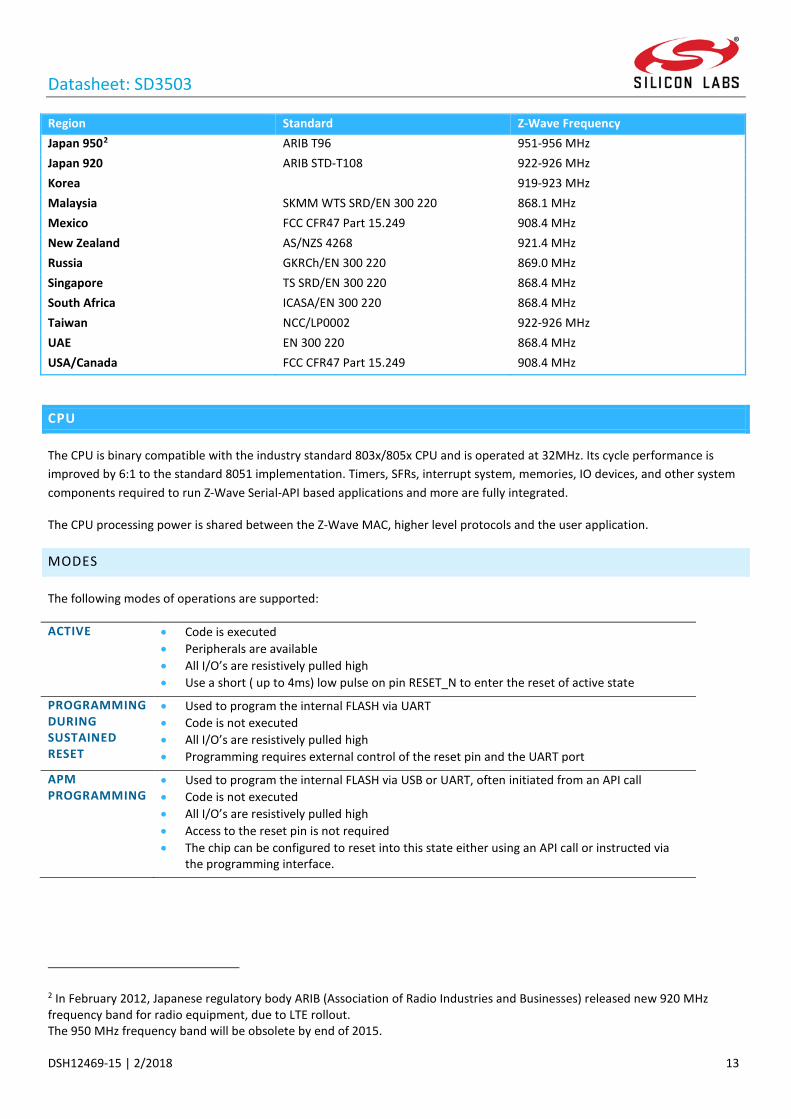
Figure 13 Schematic: System interfaces
SD3503/RF
VSS
XQ1
RF_I
O
XQ2
AVDD_CO RX_09 TX_IND
AVDD_FE
AVDD_SY BG_OUT
AVDD_IF SY_DEC
3.3V
L4 500Ω@100MHz
C16 1µF
C6 68nF
C2 68pF
C3 68pF
C4 68nF
X1 32MHz
C8 20pF
C9 20pF
L2 12nH
SAW 867.9 MHz 870.1 MHz
C1 5.6pF
L1 5.6nH
L3 27nH
C13 10nF
C14 1µF
SD3503/SYS USB_DP USB_DM SPI CS
SPI SCK SPI MISO
UART RX SPI MOSI UART TX RESET
USB CON VBUS
DP DM
GND
NVM SPI CS SPI SCK SPI MISO SPI MOSI
R8/9 22 Ω
R7 1.5 kΩ
VDD
UART RX
UART TX

Datasheet: SD3503
12 DSH12469-15 | 2/2018
WIRELESS TRANSCEIVER
The wireless Transceiver comprises a 3-channel 1GHz ISM FSK narrowband radio covering all currently used and projected Z-Wave frequencies, a modem, and a base band controller.
This architecture provides an all-digital direct synthesis transmitter and a low-IF digital receiver. The Z-Wave protocol currently utilizes two key FSK/GFSK modulation schemes and 9.6 / 40 / 100 kbit/s data rates throughout a span of carrier frequencies from 865.2 to 926 MHz.
The output power of the transmitter extends across the range of -21dBm to 5dBm, as set by your application, valid for VDD = 2.3 to 3.6V, TA = -40 to +90°C.
The software-controlled digital radio offers a wide selection of features: One, two, or three channel use, a frequency agility strategy applied to enhance network robustness, and power-saving RSSI usage. Regional enforced listen-before-talk constraints, data rate selection sets, signaling formats, and carrier frequencies can be configured to match the geographical region and product type targeted by your product build. This set of features expands gradually with new Z-Wave software releases to closely match the expanding diversity of products being added to the home control market group. For details, refer to the API documentation for the Z-Wave software applicable for your products.
Seen from an application builder’s perspective, the complexity of handling all these features, while ensuring full interoperability with existing products, are conveniently concealed behind the simple interface presented by the Z-Wave API.
INTERFACING THE FRONT-END
The reference designs include a few external components to optimally match the impedance of the PA (transmitter) and the LNA (receiver) to the 50 Ω antenna to be connected to the single-ended chip pin “RF_IO” . The SD3503 can be used with various types of antennas. Refer to document: ‘Antennas for Short Range Devices’. Suitable PCB wires often serve directly as the antenna, while helical, whip, and other antenna types are commonly seen where performance is emphasized.
Request manufacturing PCB blueprints for your target region and antenna choice.
Z-WAVE FREQUENCY COVERAGE
Region Standard Z-Wave Frequency Australia AS/NZS 4268 921.4 MHz Brazil ANATEL Resolution 506 921.4 MHz CEPT1 EN 300 220 868.4 MHz Chile FCC CFR47 Part 15.249 908.4 MHz China CNAS/EN 300 220 868.4 MHz Hong Kong HKTA 1035 919.8 MHz India N/A 865.2 MHz
1 CEPT is the European regional organization dealing with postal and telecommunications issues and presently has 45 Members: Albania, Andorra, Austria, Azerbaijan, Belarus, Belgium, Bosnia and Herzegovina, Bulgaria, Croatia, Cyprus, Czech Republic, Denmark, Estonia, Finland, France, Germany, Greece, Hungary, Iceland, Ireland, Italy, Latvia, Liechtenstein, Lithuania, Luxembourg, Malta, Moldova, Monaco, Netherlands, Norway, Poland, Portugal, Romania, Russian Federation, San Marino, Serbia and Montenegro, Slovakia, Slovenia, Spain, Sweden, Switzerland, The former Yugoslav Republic of Macedonia, Turkey, Ukraine, United Kingdom, and Vatican.
Datasheet: SD3503
DSH12469-15 | 2/2018 13
Region Standard Z-Wave Frequency Japan 9502 ARIB T96 951-956 MHz Japan 920 ARIB STD-T108 922-926 MHz Korea 919-923 MHz Malaysia SKMM WTS SRD/EN 300 220 868.1 MHz Mexico FCC CFR47 Part 15.249 908.4 MHz New Zealand AS/NZS 4268 921.4 MHz Russia GKRCh/EN 300 220 869.0 MHz Singapore TS SRD/EN 300 220 868.4 MHz South Africa ICASA/EN 300 220 868.4 MHz Taiwan NCC/LP0002 922-926 MHz UAE EN 300 220 868.4 MHz USA/Canada FCC CFR47 Part 15.249 908.4 MHz
CPU
The CPU is binary compatible with the industry standard 803x/805x CPU and is operated at 32MHz. Its cycle performance is improved by 6:1 to the standard 8051 implementation. Timers, SFRs, interrupt system, memories, IO devices, and other system components required to run Z-Wave Serial-API based applications and more are fully integrated.
The CPU processing power is shared between the Z-Wave MAC, higher level protocols and the user application.
MODES
The following modes of operations are supported:
ACTIVE • Code is executed • Peripherals are available • All I/O’s are resistively pulled high • Use a short ( up to 4ms) low pulse on pin RESET_N to enter the reset of active state
PROGRAMMING DURING SUSTAINED RESET
• Used to program the internal FLASH via UART • Code is not executed • All I/O’s are resistively pulled high • Programming requires external control of the reset pin and the UART port
APM PROGRAMMING
• Used to program the internal FLASH via USB or UART, often initiated from an API call • Code is not executed • All I/O’s are resistively pulled high • Access to the reset pin is not required • The chip can be configured to reset into this state either using an API call or instructed via
the programming interface.
2 In February 2012, Japanese regulatory body ARIB (Association of Radio Industries and Businesses) released new 920 MHz frequency band for radio equipment, due to LTE rollout. The 950 MHz frequency band will be obsolete by end of 2015.

Datasheet: SD3503
14 DSH12469-15 | 2/2018
EXTERNAL NVM PROGRAMMING
• Used to program an external NVM (FLASH/EPROM) (optionally) wired to the SPI port • Code is not executed • All I/O’s are resistively pulled high • External NVM programming requires external control of the reset pin (plus the NVM-SPI
port)
PROGRAMMING MODE
The code space and the NVR pages of the flash can be read and programmed through the UART and the USB interface. With proper (optional) Z-Wave software loaded into the Flash, Over-The-Air reprogramming will be available to your application.
ENTERING PROGRAMMING MODE
To enter programming mode, assert the RESET_N pin low for 5.2ms. The chip will then listen on the UART port for a correct initiating command.
Additionally, an API function is available that configures the chip to enter programming mode after next reset (hardware- or software-initiated). In this state only, the chip begins listening for the initiating string on the USB port as well as on the UART.
PERIPHERALS AND AUXILIARY BLOCKS
The peripherals and auxiliary blocks, other than the Z-Wave radio already outlined on page 12, will be explained in the following sections.
SUPPLY SYSTEM
The chip is powered from a single 2.3 – 3.6 V supply.
When using the schematic in Figure 14, an internal Power-On-Reset circuit guarantees that execution never begins unless the supply voltage is sufficient. The internal Brown-Out-Reset (BOR) circuit guarantees that the chip is always reset before insufficient voltage levels cause execution to fail. These guarantees apply equally in all active and power-down modes. Further, there is no restriction on power- up rise time to consider when designing an application.
On-chip supply regulators derive all the 1.5 V and 2.5 V internal supplies needed by MCU core logic, data persistency registers, the flash, and the analogue circuitry. Decoupling capacitors are required as indicated.
SD3503 SYS PWR
DVDD_IO2 DVDD_IO3 BASIC DVDD_IO4 DVDD0 MCU DVDD1 VSS VDDQ
3.3V
C4 68nF
C5 68nF
C10 6.8nF
C11 68nF
C12 6.8nF
C15 1µF

Datasheet: SD3503
DSH12469-15 | 2/2018 15
Figure 14: Supply related external components
Note that digital IO circuits are powered unregulated via the supply pins. As a consequence, for the internal USB PHY to be signaling level compliant when in use, the supply must be set to 3.0 – 3.6 V.
XTAL AND SYSTEM CLOCK
The SD3503 derives RF frequencies and MCU clocks from an external 32MHz crystal (XTAL) as shown in Figure 12: Schematic: Z-Wave RF enabled on page 11.
Refer to your crystal component supplier for suitable load capacitance values, or refer to the BOM on our published reference designs.
PRODUCTION CONSIDERATIONS
Silicon Labs specifies application of a reference clock during the system test/calibration step to guarantee initial frequency precision. Request the applicable application note. A built-in frequency calibration circuit compensates for initial crystal frequency offsets of up to ±100 ppm.
The temperature and 5 years aging margin for the 32MHz crystal is 15 ppm.
To ensure frequency shift keying is kept within the 10% accuracy range specified by ITU-T G.9959, the device should be allowed to self-calibrate using a procedure built into all supported programmers.
WAKE-UP-TIMER
The max 200nA built-in WUT (Wake Up Timer) plays an important role in maximizing battery life of applications like Frequently Listening Routing Slave (FLIRS) Z-Wave nodes. The WUT is also available to customer applications, and may be programmed to wake a sleeping node after 0 to 256 seconds of sleep. The programming resolution equals 8 bit fractions of 2 seconds, alternatively 8 bit fractions of 256 seconds.
The WUT is autonomously calibrated to the system clock (whenever this is running) and maintains a better than 2% precision.
BATTERY MONITOR ADC
The monitor raises an interrupt if a lower or an upper warning supply threshold is exceeded. The sample rate versus accuracy tradeoff options (in continuous mode) are:
• 20 kHz 8 bit mode • 10 kHz 12 bit mode
SPI
A Serial Peripheral Interface (SPI) is available on pins 14, 16-18. The SPI enables synchronous data transfers between this and slave SPI devices.
Pin SPI Pin SPI Function, master Pin 18 MOSI Data output Pin 17 MISO Data input Pin 16 SCK Clock output Pin 14 SS Slave Selects output
Datasheet: SD3503
16 DSH12469-15 | 2/2018
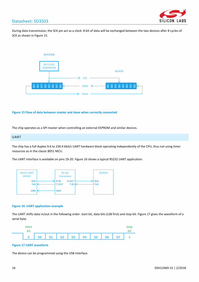
During data transmission, the SCK pin act as a clock. 8 bit of data will be exchanged between the two devices after 8 cycles of SCK as shown in Figure 15.
Figure 15 Flow of data between master and slave when correctly connected
The chip operates as a SPI master when controlling an external EEPROM and similar devices.
UART
The chip has a full duplex 9.6 to 230.4 kbit/s UART hardware block operating independently of the CPU, thus not using timer resources as in the classic 8051 MCU.
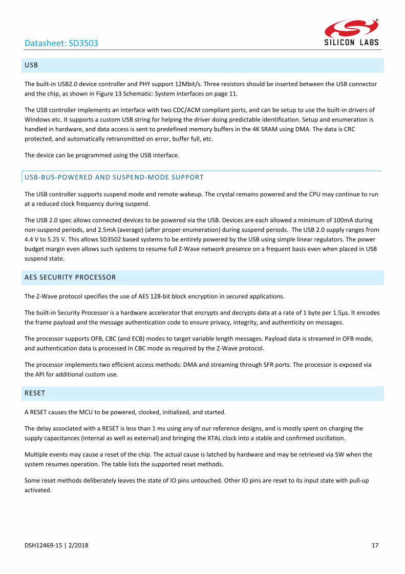
The UART interface is available on pins 19-20. Figure 16 shows a typical RS232 UART application.
Figure 16: UART application example
The UART shifts data in/out in the following order: start bit, data bits (LSB first) and stop bit. Figure 17 gives the waveform of a serial byte.
Start bit
Stop bit
0 D0 D1 D2 D3 D4 D5 D6 D7 1
Figure 17 UART waveform
The device can be programmed using the USB interface.
SPI CLOCK GENERATOR
MASTER
0 0 1 0 0 0 1 0
SCK
MISO
MOSI
0 0 1 0 0 0 1 0
SLAVE
RS232 UART DEVICE
RxD TxD
GND
SD3503
RxD TxD
RS 232 Transceiver
R-IN T-OUT GND
R-OUT T-IN
Datasheet: SD3503
DSH12469-15 | 2/2018 17
USB
The built-in USB2.0 device controller and PHY support 12Mbit/s. Three resistors should be inserted between the USB connector and the chip, as shown in Figure 13 Schematic: System interfaces on page 11.
The USB controller implements an interface with two CDC/ACM compliant ports, and can be setup to use the built-in drivers of Windows etc. It supports a custom USB string for helping the driver doing predictable identification. Setup and enumeration is handled in hardware, and data access is sent to predefined memory buffers in the 4K SRAM using DMA. The data is CRC protected, and automatically retransmitted on error, buffer full, etc.
The device can be programmed using the USB interface.
USB-BUS-POWERED AND SUSPEND-MODE SUPPORT
The USB controller supports suspend mode and remote wakeup. The crystal remains powered and the CPU may continue to run at a reduced clock frequency during suspend.
The USB 2.0 spec allows connected devices to be powered via the USB. Devices are each allowed a minimum of 100mA during non-suspend periods, and 2.5mA (average) (after proper enumeration) during suspend periods. The USB 2.0 supply ranges from 4.4 V to 5.25 V. This allows SD3502 based systems to be entirely powered by the USB using simple linear regulators. The power budget margin even allows such systems to resume full Z-Wave network presence on a frequent basis even when placed in USB suspend state.
AES SECURITY PROCESSOR
The Z-Wave protocol specifies the use of AES 128-bit block encryption in secured applications.
The built-in Security Processor is a hardware accelerator that encrypts and decrypts data at a rate of 1 byte per 1.5µs. It encodes the frame payload and the message authentication code to ensure privacy, integrity, and authenticity on messages.
The processor supports OFB, CBC (and ECB) modes to target variable length messages. Payload data is streamed in OFB mode, and authentication data is processed in CBC mode as required by the Z-Wave protocol.
The processor implements two efficient access methods: DMA and streaming through SFR ports. The processor is exposed via the API for additional custom use.
RESET
A RESET causes the MCU to be powered, clocked, initialized, and started.
The delay associated with a RESET is less than 1 ms using any of our reference designs, and is mostly spent on charging the supply capacitances (internal as well as external) and bringing the XTAL clock into a stable and confirmed oscillation.
Multiple events may cause a reset of the chip. The actual cause is latched by hardware and may be retrieved via SW when the system resumes operation. The table lists the supported reset methods.
Some reset methods deliberately leaves the state of IO pins untouched. Other IO pins are reset to its input state with pull-up activated.
Datasheet: SD3503
18 DSH12469-15 | 2/2018
Reset Cause Description Effect on IO state POR Reset request generated by Power-On-
Reset hardware Reset
BOR Reset request generated by Brown-Out-Reset hardware
Reset
RESET_N Reset request generated by the RESET_N pin being de-asserted
Reset
WUT Reset request generated by the Wake-Up-Timer timing out
Untouched
WATCHDOG Reset request generated by the WATCHDOG Timer timing out
Reset
Software Reset by software Untouched
PIN DESCRIPTIONS
PINS: 900 MHZ Z-WAVE RADIO
Function Pad identification Type Antenna Pin 4: RF IO 1.5V RF analogue Connection points for RF impedance matching components
Pin 3: RF Tx inductor 1.5V RF analogue Pin 5: RF Rx 900MHz inductor 1.5V RF analogue
Connection points for other external components needed to support Z-Wave (e.g. capacitors)
Pin 2: Power for RF front end 1.5V analogue Pin 6: Power for synthesizer and bandgab 1.5V analogue Pin 8: BandGab voltage OUT 1.5V analogue Pin 7: Synthesizer Decoupler Capacitor 1.5V analogue Pin 9: Power for analog IF 1.5V analogue Pin 31: Power for analog core 1.5V analogue
PINS: SYSTEM INTERFACE
Function Pad identification Type USB Pin 24: USB negative IO 3.3V IO
Pin 25: USB positive IO 3.3V IO UART Pin 20: UART 0 RX 3.3V IO
Pin 19: UART 0 TX 3.3V IO SPI (for serial Flash) Pin 18: SPI 0 MOSI 3.3V IO
Pin 17: SPI 0 MISO 3.3V IO Pin 16: SPI 0 SCK 3.3V IO Pin 14: SS 3.3V IO
System reset Pin 15: RESET_N 3.3V IO Clock XTAL Pin 1: Clock Oscillator output 1.5V analogue
Pin 32: Clock Oscillator input 1.5V analogue
Power supply 3.3V Pin 21: Digital IO Power 3.3V Supply Pin 22: Digital IO Power 3.3V Supply Pin 26: Digital IO Power 3.3V Supply
Pin 27: Digital domain power 3.3V Supply Pin 28: Digital domain power 3.3V Supply Connection points for other external components needed to support the system (e.g. capacitors)
Pin 23: Power for Flash 2.5V Pin 29: Internal Power 1.5V 1.5V Pin 30: Internal Power 1.5V 1.5V
Datasheet: SD3503
DSH12469-15 | 2/2018 19
PINS PER PIN NUMBER
No Name Type Description pin 1 XOSC_Q2 IO for XTAL Clock Oscillator (output) pin 2 AVDD_FE VDD 3.3V Power for RF front end pin 3 TX_IND Analogue RF RF Tx inductor pin 4 RF_IO Analogue RF IO RF IO (antenna path) pin 5 RX_09 Analogue RF RF RX 900MHz inductor pin 6 AVDD_SY VDD 3.3V Power for synthesizer and bandgap pin 7 SY_DECOUP 1.5V Internal supply Synthesizer supply pin 8 BG_OUT Analogue 1.5V domain Bandgap voltage OUT pin 9 AVDD_IF VDD 3.3V Power for analog IF pin 10 N.C. N.C. Not Connected pin 11 N.C N.C. Not Connected. Reserved. Pin 12 N.C N.C. Not Connected. Reserved. pin 13 N.C. N.C. Not Connected pin 14 P1_5 3.3V digital IO SPI0 CS (active low) pin 15 RESET_N 3.3V digital IO System reset / pgm interface3 pin 16 P2_7 3.3V digital IO SPI0 SCK pin 17 P2_6 3.3V digital IO SPI0 MISO pin 18 P2_5 3.3V digital IO SPI0 MOSI pin 19 P2_1 3.3V digital IO UART0 TX / pgm interface pin 20 P2_0 3.3V digital IO UART0 RX / pgm interface pin 21 DVDD_IO2 VDD 3.3V Digital IO power 2 / pgm interface pin 22 DVDD_IO3 VDD 3.3V Digital IO power 3 pin 23 VDDQ Analogue IO 3.3V domain Power for Flash (output of charge pump) pin 24 USB_DM 3.3V digital IO USB negative diff IO / USB ISP pin 25 USB_DP 3.3V digital IO USB positive diff IO / USB ISP / pgm interface (calibration) pin 26 DVDD_IO4 VDD 3.3V Digital IO power 4 pin 27 DVDD0 VDD 3.3V Digital domain power 0 pin 28 DVDD1 VDD 3.3V Digital domain power 1 pin 29 MCU 1.5V Internal supply Internal Power 1.5V (MCU) pin 30 BASIC 1.5V Internal supply Internal Power 1.5V (BASIC) pin 31 AVDD_AC0 VDD 3.3V Power for Analog core pin 32 XOSC_Q1 IO for XTAL Clock Oscillator (input) Exposed GND GND Exposed center pad/ pgm interface
PROCESS SPECIFICATION
Specification Description
MSL 3 Moisture Sensitivity Level tested according to JEDEC J-STD-020C REACH REACH is a European Community Regulation on chemicals and their safe use (EC 1907/2006).
It deals with the Registration, Evaluation, Authorisation and Restriction of Chemical substances
RoHS Designed in compliance with The Restriction of Hazardous Substances Directive (RoHS)
3 The pins marked “/ pgm interface” constitute the programming and debugging interface. This interface must be exposed to the programmer if In-System Programming is required. Please refer to INS12213 Instruction: 500 Series Integration Guide.

Datasheet: SD3503
20 DSH12469-15 | 2/2018
PCB MOUNTING AND SOLDERING
RECOMMENDED PCB MOUNTING PATTERN
Please follow standard QFN mounting pattern.
SOLDERING INFORMATION
The soldering details to properly solder the SD3502 module on standard PCBs are described below. The information provided is intended only as a guideline and Silicon Labs is not liable if a selected profile does not work.
See IPC/JEDEC J-STD-020D.1 for more information.
PCB solder mask expansion from landing pad edge 0.1 mm PCB paste mask expansion from landing pad edge 0.0 mm PCB process Pb-free (Lead free for RoHS 4compliance) PCB finish Defined by the manufacturing facility (EMS) or customer Stencil aperture Defined by the manufacturing facility (EMS) or customer Stencil thickness Defined by the manufacturing facility (EMS) or customer Solder paste used Defined by the manufacturing facility (EMS) or customer Flux cleaning process Defined by the manufacturing facility (EMS) or customer
Figure 18 Recommended Reflow Temperature Profile
4 RoHS = Restriction of Hazardous Substances Directive, EU

Datasheet: SD3503
DSH12469-15 | 2/2018 21
ORDERING INFORMATION
Part Number Product Description SD3503A-CNE3R 2000 pcs QFN 32 pins 5x5 mm on reel
PACKAGE
QFN 32 PINS 5X5 MM
Caution: Moisture sensitive device MSL-3 defined by IPC/JEDEC J-STD-020. May require bake before mounting after bag is opened.
Symbol Min Nom Max
Datasheet: SD3503
22 DSH12469-15 | 2/2018
Total thickness A 0.7 0.75 0.8 Stand off A1 0 0.035 0.05 Mold thickness A2 --- 0.55 0.57 L/F thickness A3 0.203 REF Leak width b 0.2 0.25 0.3 Body size D (x) 5 BSC
E (y) 5 BSC Lead pitch e 0.5 BSC EP size J (x) 3.4 3.5 3.6
K (y) 3.4 3.5 3.6 Lead length L 0.35 0.4 0.45 Package edge tolerance aaa 0.1 Mold flatness bbb 0.1 Co-planarity ccc 0.08 Lead offset ddd 0.1 Exposed pad offset eee 0.1
REEL
W1 12.4mm – 12.6mm W2 18.4mm (max) Ø N 100mm (min)
Ø A 330mm (max)

Datasheet: SD3503
DSH12469-15 | 2/2018 23
Parameter Value Pin 1 Quadrant Pocket Quadrant Q1
Datasheet: SD3503
24 DSH12469-15 | 2/2018
TOP MARKING
Marking
Meaning
SD3503 Product number A Product revision C Commercial temperature range N QFN package E3 Green BOM LLLL… Wafer lot YYWW TWN YY [year]
WW [week] TWN [Country of Origin]
Datasheet: SD3503
DSH12469-15 | 2/2018 25
DOCUMENT CHANGE LIST
Version Date By Pages affected Description of changes
1 2013-02-22 PNI All Initial draft 2 2013-05-13 PNI 7 Sensitivity versus Temperature graph added 3 2013-05-17 PNI 7 Added typical current consumption versus TX power
All Edits from technical writer committed 4 2013-05-31 PNI 8-9 IO data updated 5 2013-06-03 PNI All Repaired header and footers 6 2013-08-16 PNI 19-21 Ordering info updated, changing to reels 7 2013-09-30 PNI 9 Pull up resistor characteristics added 8 2013-10-14 PNI 18-19 Package drawing and dim table replaced 9 2013-11-29 PNI 6 Added typical blocking versus bit rate
10 2013-11-12 PNI 13-14 Operating modes section updated 11 2014-01-05 PNI 18 Pin list table inserted 12 2014-03-11 PNI 18 P/N now appended with an R (to emphasize the Reel packaging) 13 2014-03-14 PNI 18 RESET0_N corrected to RESET_N 13 2014-04-22 PNI 9, 18-19 Storage temperature added, programming pin notifications, MSL3
specified 13 2014-04-28 PNI 11-12 Table “Z WAVE FREQUENCY COVERAGE” updated 14 2014-06-11 PNI 12 Improper reference to SPI deleted 15 2015-03-27 MHANSEN 20
19 23
Added section PCB mounting and soldering Added section Process Specification Added orientation of component in tape

http://www.silabs.com
Silicon Laboratories Inc.400 West Cesar ChavezAustin, TX 78701USA
Smart. Connected. Energy-Friendly.
Productswww.silabs.com/products
Qualitywww.silabs.com/quality
Support and Communitycommunity.silabs.com
DisclaimerSilicon Labs intends to provide customers with the latest, accurate, and in-depth documentation of all peripherals and modules available for system and software implementers using or intending to use the Silicon Labs products. Characterization data, available modules and peripherals, memory sizes and memory addresses refer to each specific device, and "Typical" parameters provided can and do vary in different applications. Application examples described herein are for illustrative purposes only. Silicon Labs reserves the right to make changes without further notice and limitation to product information, specifications, and descriptions herein, and does not give warranties as to the accuracy or completeness of the included information. Silicon Labs shall have no liability for the consequences of use of the information supplied herein. This document does not imply or express copyright licenses granted hereunder to design or fabricate any integrated circuits. The products are not designed or authorized to be used within any Life Support System without the specific written consent of Silicon Labs. A "Life Support System" is any product or system intended to support or sustain life and/or health, which, if it fails, can be reasonably expected to result in significant personal injury or death. Silicon Labs products are not designed or authorized for military applications. Silicon Labs products shall under no circumstances be used in weapons of mass destruction including (but not limited to) nuclear, biological or chemical weapons, or missiles capable of delivering such weapons.
Trademark InformationSilicon Laboratories Inc.® , Silicon Laboratories®, Silicon Labs®, SiLabs® and the Silicon Labs logo®, Bluegiga®, Bluegiga Logo®, Clockbuilder®, CMEMS®, DSPLL®, EFM®, EFM32®, EFR, Ember®, Energy Micro, Energy Micro logo and combinations thereof, "the world’s most energy friendly microcontrollers", Ember®, EZLink®, EZRadio®, EZRadioPRO®, Gecko®, ISOmodem®, Micrium, Precision32®, ProSLIC®, Simplicity Studio®, SiPHY®, Telegesis, the Telegesis Logo®, USBXpress®, Zentri, Z-Wave and others are trademarks or registered trademarks of Silicon Labs. ARM, CORTEX, Cortex-M3 and THUMB are trademarks or registered trademarks of ARM Holdings. Keil is a registered trademark of ARM Limited. All other products or brand names mentioned herein are trademarks of their respective holders.