Embed Size (px)
Citation preview

LT3689/LT3689-5
13689fe
For more information www.linear.com/LT3689
TYPICAL APPLICATION
FEATURES
APPLICATIONS
DESCRIPTION
700mA Step-Down Regulator with Power-On Reset
and Watchdog Timer
The LT®3689 is an adjustable frequency (350kHz to 2.2MHz) monolithic step-down switching regulator with a power-on reset and watchdog timer. The regulator operates from inputs up to 36V and withstands transients up to 60V. Low ripple Burst Mode® operation maintains high efficiency at low output current while keeping output ripple below 15mV in a typical application, with input quiescent current of just 85µA. Shutdown circuitry reduces input supply current to less than 1µA while EN/UVLO is pulled low. Using a resis-tor divider on the EN/UVLO pin provides a programmable undervoltage lockout. Current limit, frequency foldback and thermal shutdown provide fault protection.
The reset and watchdog timeout periods are indepen-dently adjustable using external capacitors. Tight accuracy specifications and glitch immunity ensure reliable reset operation of a system without false triggering. The open collector RST will pull down if output voltage drops 10% below the programmed value. The watchdog timer is pin-selectable for window or timeout modes. In timeout mode, WDO pulls low if too long of a period passes before a watchdog transition is detected. In window mode, the LT3689 monitors for WDI falling edges grouped too close together or too far apart.L, LT, LTC, LTM, Linear Technology, the Linear logo and Burst Mode are registered trademarks of Linear Technology Corporation. All other trademarks are the property of their respective owners.
3.3V Regulator with Power-On Reset Timer and Watchdog Timer
n Wide Input Range: Operation from 3.6V to 36V Overvoltage Lockout Protects Circuits through 60V Transients
n 85µA IQ at 12VIN to 3.3VOUT n Low Ripple Burst Mode® Operation Allows Output
Ripple <15mVP-P n Programmable, Defeatable Watchdog Timer with
Window or Timeout Controln Programmable Power-On Reset Timer (POR)n Synchronizable, Adjustable 350kHz to 2.2MHz
Switching Frequency n 700mA Output Switching Regulator with Internal
Power Switchn Fixed 5V or Adjustable Output Voltagen 800mV Feedback Voltagen Programmable Input Undervoltage Lockout with
Hysteresisn 16-Pin 3mm × 3mm QFN and 16-Pin MSOP Packages
n Automotive Electronic Control Unitsn Industrial Power Supplies
SWI/O
I/O
RESET DAFBRT
SYNC
fSW = 700kHz
WDI
RST
WDO
VIN
µP
EN/UVLO
VIN4.5V TO 36V
TRANSIENT TO 60V
3.3V700mA
100k
CWDT10nF
tWDU = 182mstWDL = 5.9ms
12µH
10pF
22µF
0.1µF
316k
GND 20.5k
LT3689
3689 TA01
BSTOUT
CPOR
CWDT
2.2µF
CPOR68nF
tRST = 157ms
Efficiency
LOAD CURRENT (A)
EFFI
CIEN
CY (%
)
POWER LOSS (m
W)
0.0001 0.01 0.1 10.001
3689 TA01b
VIN = 12VVOUT = 3.3Vf = 700kHzL = 12µHTA = 25°C
40
50
60
70
80
30
20
10
0
90
100
10
1
1000

LT3689/LT3689-5
23689fe
For more information www.linear.com/LT3689
ABSOLUTE MAXIMUM RATINGSVIN, EN/UVLO Voltage (Note 2) .................................60VBST Voltage ..............................................................60VBST Above SW Voltage .............................................30VOUT, WDE Voltage ....................................................30VFB, RT, SYNC, W/T, WDI, RST, WDO Voltage ..............6VCWDT, CPOR Voltage ....................................................3V
(Note 1)
ORDER INFORMATIONLEAD FREE FINISH TAPE AND REEL PART MARKING* PACKAGE DESCRIPTION TEMPERATURE RANGE
LT3689EMSE#PBF LT3689EMSE#TRPBF 3689 16-Lead Plastic MSOP with Exposed Pad –40°C to 125°C
LT3689IMSE#PBF LT3689IMSE#TRPBF 3689 16-Lead Plastic MSOP with Exposed Pad –40°C to 125°C
LT3689HMSE#PBF LT3689HMSE#TRPBF 3689 16-Lead Plastic MSOP with Exposed Pad –40°C to 150°C
LT3689EMSE-5#PBF LT3689EMSE-5#TRPBF 36895 16-Lead Plastic MSOP with Exposed Pad –40°C to 125°C
LT3689IMSE-5#PBF LT3689IMSE-5#TRPBF 36895 16-Lead Plastic MSOP with Exposed Pad –40°C to 125°C
LT3689HMSE-5#PBF LT3689HMSE-5#TRPBF 36895 16-Lead Plastic MSOP with Exposed Pad –40°C to 150°C
LT3689EUD#PBF LT3689EUD#TRPBF LDND 16-Lead (3mm × 3mm) Plastic QFN –40°C to 125°C
LT3689IUD#PBF LT3689IUD#TRPBF LDND 16-Lead (3mm × 3mm) Plastic QFN –40°C to 125°C
LT3689EUD-5#PBF LT3689EUD-5#TRPBF LFFM 16-Lead (3mm × 3mm) Plastic QFN –40°C to 125°C
LT3689IUD-5#PBF LT3689IUD-5#TRPBF LFFM 16-Lead (3mm × 3mm) Plastic QFN –40°C to 125°C
Consult LTC Marketing for parts specified with wider operating temperature ranges. *The temperature grade is identified by a label on the shipping container.Consult LTC Marketing for information on non-standard lead based finish parts.For more information on lead free part marking, go to: http://www.linear.com/leadfree/ For more information on tape and reel specifications, go to: http://www.linear.com/tapeandreel/
12345678
WDOCWDTCPOR
RTSYNC
OUTBSTVIN
161514131211109
RSTWDIW/TWDEFBEN/UVLODASW
TOP VIEW
17
MSE PACKAGE16-LEAD PLASTIC MSOP
θJA = 43°C/W, θJC = 4.3°C/W EXPOSED PAD (PIN 17) IS GND, MUST BE SOLDERED TO PCB
16 15 14 13
5 6
17
7 8
TOP VIEW
UD PACKAGE16-LEAD (3mm × 3mm) PLASTIC QFN
9
10
11
12
4
3
2
1BST
VIN
SW
DA
CWDT
WDO
RST
WDI
OUT
SYNC
RT C POR
EN/U
VLO FB
WDE
W/T
θJA = 68°C/W, θJC = 4.2°C/W
EXPOSED PAD (PIN 17) IS GND, MUST BE SOLDERED TO PCB
PIN CONFIGURATION
Operating Junction Temperature Range (Note 3) LT3689E ............................................ –40°C to 125°C LT3689I ............................................. –40°C to 125°C LT3689H ............................................ –40°C to 150°CStorage Temperature Range .................. –65°C to 150°CLead Temperature (Soldering, 10 sec)
MSOP ............................................................... 300°C
LT3689/LT3689-5
33689fe
For more information www.linear.com/LT3689
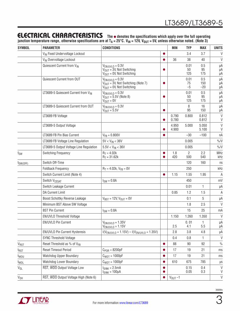
ELECTRICAL CHARACTERISTICS
SYMBOL PARAMETER CONDITIONS MIN TYP MAX UNITS
VIN Fixed Undervoltage Lockout l 3.4 3.7 V
VIN Overvoltage Lockout l 36 38 40 V
Quiescent Current from VIN VEN/UVLO = 0.3V VOUT = 3V, Not Switching VOUT = 0V, Not Switching
l
0.01 50
125
0.5 95
175
µA µA µA
Quiescent Current from OUT VEN/UVLO = 0.3V VOUT = 3V, Not Switching (Note 7) VOUT = 0V, Not Switching
l
0.01 75 –5
0.5 150 –20
µA µA µA
LT3689-5 Quiescent Current from VIN VEN/UVLO = 0.3V VOUT = 5.5V (Note 8) VOUT = 0V
l
0.01 50
125
0.5 95
175
µA µA µA
LT3689-5 Quiescent Current from OUT VEN/UVLO = 0.3V VOUT = 5.5V
l
8 95
16 150
µA µA
LT3689 FB Voltage
l
0.790 0.780
0.800 0.812 0.812
V V
LT3689-5 Output Voltage
l
4.950 4.900
5.000 5.050 5.100
V V
LT3689 FB Pin Bias Current VFB = 0.800V l –30 –100 nA
LT3689 FB Voltage Line Regulation 5V < VIN < 36V 0.005 %/V
LT3689-5 Output Voltage Line Regulation 5.5V < VIN < 36V 0.005 %/V
fSW Switching Frequency RT = 4.02k RT = 31.62k
l
l
1.8 420
2 500
2.2 540
MHz kHz
tSW(OFF) Switch Off-Time 120 160 ns
Foldback Frequency RT = 4.02k, VFB = 0V 250 kHz
Switch Current Limit (Note 4) l 1.15 1.55 1.95 A
Switch VCESAT ISW = 0.8A 450 mV
Switch Leakage Current 0.01 1 µA
DA Current Limit 0.85 1.2 1.5 A
Boost Schottky Reverse Leakage VBST = 12V, VOUT = 0V 0.1 5 µA
Minimum BST Above SW Voltage 1.8 2.5 V
BST Pin Current ISW = 0.8A 15 25 mA
EN/UVLO Threshold Voltage 1.150 1.260 1.350 V
EN/UVLO Pin Current VEN/UVLO = 1.35V VEN/UVLO = 1.15V
2.5
0. 01 4.1
1 5.5
µA µA
EN/UVLO Pin Current Hysteresis I(VEN/UVLO = 1.15V) – I(VEN/UVLO = 1.35V) 2.8 3.8 4.8 µA
SYNC Threshold Voltage 0.4 0.8 1 V
VRST Reset Threshold as % of VFB l 88 90 92 %
tRST Reset Timeout Period CPOR = 8200pF l 17 19 21 ms
tWDU Watchdog Upper Boundary CWDT = 1000pF l 17 19 21 ms
tWDL Watchdog Lower Boundary CWDT = 1000pF l 610 675 785 µs
VOL RST, WDO Output Voltage Low ISINK = 2.5mA ISINK = 100µA
l
l
0.15 0.05
0.4 0.3
V V
VOH RST, WDO Output Voltage High (Note 6) l VOUT –1 V
The l denotes the specifications which apply over the full operating junction temperature range, otherwise specifications are at TA = 25°C. VIN = 12V, VOUT = 5V, unless otherwise noted. (Note 3)
LT3689/LT3689-5
43689fe
For more information www.linear.com/LT3689
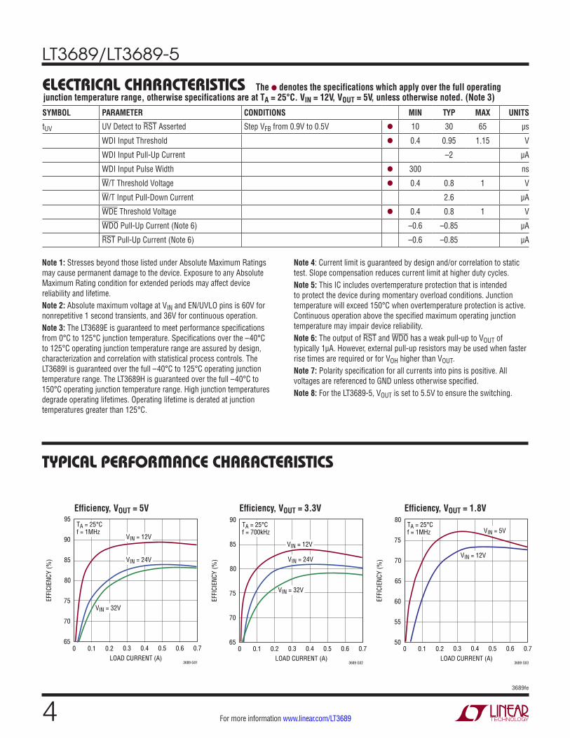
SYMBOL PARAMETER CONDITIONS MIN TYP MAX UNITS
tUV UV Detect to RST Asserted Step VFB from 0.9V to 0.5V l 10 30 65 µs
WDI Input Threshold l 0.4 0.95 1.15 V
WDI Input Pull-Up Current –2 µA
WDI Input Pulse Width l 300 ns
W/T Threshold Voltage l 0.4 0.8 1 V
W/T Input Pull-Down Current 2.6 µA
WDE Threshold Voltage l 0.4 0.8 1 V
WDO Pull-Up Current (Note 6) –0.6 –0.85 µA
RST Pull-Up Current (Note 6) –0.6 –0.85 µA
Note 1: Stresses beyond those listed under Absolute Maximum Ratings may cause permanent damage to the device. Exposure to any Absolute Maximum Rating condition for extended periods may affect device reliability and lifetime.Note 2: Absolute maximum voltage at VIN and EN/UVLO pins is 60V for nonrepetitive 1 second transients, and 36V for continuous operation.Note 3: The LT3689E is guaranteed to meet performance specifications from 0°C to 125°C junction temperature. Specifications over the –40°C to 125°C operating junction temperature range are assured by design, characterization and correlation with statistical process controls. The LT3689I is guaranteed over the full –40°C to 125°C operating junction temperature range. The LT3689H is guaranteed over the full –40°C to 150°C operating junction temperature range. High junction temperatures degrade operating lifetimes. Operating lifetime is derated at junction temperatures greater than 125°C.
Note 4: Current limit is guaranteed by design and/or correlation to static test. Slope compensation reduces current limit at higher duty cycles. Note 5: This IC includes overtemperature protection that is intended to protect the device during momentary overload conditions. Junction temperature will exceed 150°C when overtemperature protection is active. Continuous operation above the specified maximum operating junction temperature may impair device reliability. Note 6: The output of RST and WDO has a weak pull-up to VOUT of typically 1µA. However, external pull-up resistors may be used when faster rise times are required or for VOH higher than VOUT.Note 7: Polarity specification for all currents into pins is positive. All voltages are referenced to GND unless otherwise specified.Note 8: For the LT3689-5, VOUT is set to 5.5V to ensure the switching.
ELECTRICAL CHARACTERISTICS The l denotes the specifications which apply over the full operating junction temperature range, otherwise specifications are at TA = 25°C. VIN = 12V, VOUT = 5V, unless otherwise noted. (Note 3)
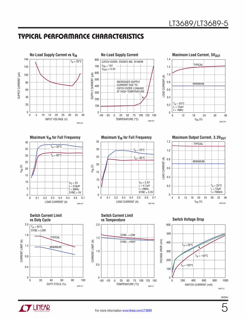
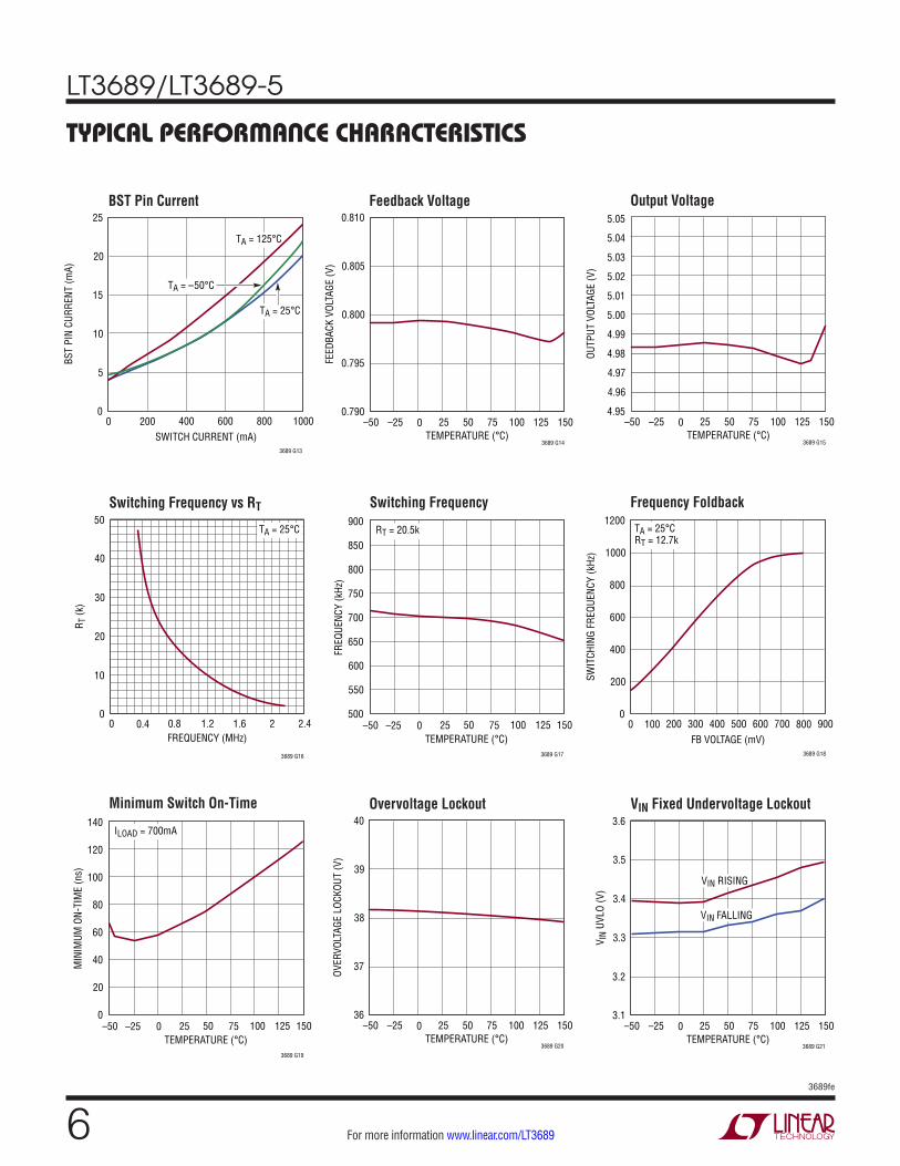
TYPICAL PERFORMANCE CHARACTERISTICS
Efficiency, VOUT = 5V Efficiency, VOUT = 3.3V Efficiency, VOUT = 1.8V
LOAD CURRENT (A)0
EFFI
CIEN
CY (%
)
0.40.2 0.60.30.1 0.5 0.7
3689 G01
TA = 25°Cf = 1MHz
VIN = 12V
VIN = 24V
VIN = 32V
85
90
80
75
70
65
95
0 0.40.2 0.60.30.1 0.5 0.7LOAD CURRENT (A)
EFFI
CIEN
CY (%
)
85
80
75
70
65
90
3689 G02
TA = 25°Cf = 700kHz
VIN = 12V
VIN = 24V
VIN = 32V
LOAD CURRENT (A)
EFFI
CIEN
CY (%
) 70
75
65
60
55
50
80
3689 G03
TA = 25°Cf = 1MHz VIN = 5V
VIN = 12V
0 0.40.2 0.60.30.1 0.5 0.7
LT3689/LT3689-5
53689fe
For more information www.linear.com/LT3689
TYPICAL PERFORMANCE CHARACTERISTICS
No-Load Supply Current vs VIN No-Load Supply Current Maximum Load Current, 5VOUT
Maximum Output Current, 3.3VOUT
Switch Current Limit vs Duty Cycle
Switch Current Limit vs Temperature Switch Voltage Drop
Maximum VIN for Full FrequencyMaximum VIN for Full Frequency
INPUT VOLTAGE (V)0
SUPP
LY C
URRE
NT (µ
A)
80
100
120
35
60
40
10 205 15 25 30 40
20
0
140
3689 G04
TA = 25°C
TEMPERATURE (°C)–50
0
SUPP
LY C
URRE
NT (µ
A)
200
400
600
–25 0 25 50 10075 125
800
100
300
500
700
150
3689 G05
CATCH DIODE: DIODES INC. B140HBVIN = 12VVOUT = 3.3V
INCREASED SUPPLYCURRENT DUE TOCATCH DIODE LEAKAGEAT HIGH TEMPERATURE
0
0.4
0.8
1.2
0.2
0.6
1.0
1.4
VIN (V)6
LOAD
CUR
RENT
(A)
12 18 3024 36
3689 G06
MINIMUM
TYPICAL
TA = 25°CL = 12µHf = 1MHz
0 0.40.2 0.60.30.1 0.5 0.7LOAD CURRENT (A)
0
V IN
(V)
10
20
30
40
5
15
25
35
3689 G07
VO = 5VL = 6.8µHf = 2MHzSYNC = 5V
TA = 25°C
TA = 85°C
0 0.40.2 0.60.30.1 0.5 0.7LOAD CURRENT (A)
0
V IN
(V)
10
20
30
5
15
25
35
3689 G08
VO = 3.3VL = 4.7µHf = 2MHzSYNC = 3.3V
TA = 25°C
TA = 85°C
VIN (V)4
0
LOAD
CUR
RENT
(A)
0.4
0.8
1.2
8 12 16 20 2824 32
0.2
0.6
1.0
36
3689 G09
TA = 25°CL = 12µHf = 700kHz
MINIMUM
TYPICAL
DUTY CYCLE (%)0
0
CURR
ENT
LIM
IT (A
)
0.4
0.8
1.2
1.6
2.0
20 40 60 80 100
3689 G10
TA = 25°CSYNC = LOW
MINIMUM
TYPICAL
TEMPERATURE (°C)
0
CURR
ENT
LIM
IT (A
)
0.5
1.0
1.5
2.0
3689 G11
SYNC = HIGH
SYNC = LOW
–50 –25 0 25 50 10075 125 150SWITCH CURRENT (mA)
0
VOLT
AGE
DROP
(mV)
400
500
300
200
400 800200 600 1000
100
0
600
3689 G12
TA = 125°C
TA = 25°C
TA = –50°C
LT3689/LT3689-5
63689fe
For more information www.linear.com/LT3689
TYPICAL PERFORMANCE CHARACTERISTICS
Switching Frequency vs RT Switching Frequency Frequency Foldback
Minimum Switch On-Time Overvoltage Lockout VIN Fixed Undervoltage Lockout
BST Pin Current Feedback Voltage
SWITCH CURRENT (mA)0
BST
PIN
CURR
ENT
(mA)
15
20
10
5
400 800200 600 10000
25
3689 G13
TA = 125°C
TA = –50°C
TA = 25°C
TEMPERATURE (°C)
0.790
FEED
BACK
VOL
TAGE
(V)
0.795
0.800
0.805
0.810
3689 G14
–50 –25 0 25 50 10075 125 150
FREQUENCY (MHz)0
0
R T (k
)
10
20
30
40
50
0.4 0.8 1.2 1.6
3689 G16
2 2.4
TA = 25°C
TEMPERATURE (°C)
500
FREQ
UENC
Y (k
Hz)
600
700
800
900
550
650
750
850
3689 G17
–50 25 75–25 0 50 100 150125
RT = 20.5k
FB VOLTAGE (mV)0
SWIT
CHIN
G FR
EQUE
NCY
(kHz
)800
1000
600
400
200 300 500100 400 600 800700 900
200
0
1200
3689 G18
TA = 25°CRT = 12.7k
TEMPERATURE (°C)
0
MIN
IMUM
ON-
TIM
E (n
s)
20
60
100
140
40
80
120
3689 G19
–50 25 75–25 0 50 100 150125
ILOAD = 700mA
TEMPERATURE (°C)
36
OVER
VOLT
AGE
LOCK
OUT
(V)
37
38
39
40
3689 G20
–50 –25 0 25 50 10075 125 150TEMPERATURE (°C)
3.1
V IN
UVLO
(V)
3.2
3.3
3.4
3.5
3.6
3689 G21
VIN FALLING
VIN RISING
–50 –25 0 25 50 10075 125 150
Output Voltage
TEMPERATURE (°C)
OUTP
UT V
OLTA
GE (V
)
3689 G15
–50 –25 0 25 50 10075 125 1504.95
4.97
4.99
5.01
5.03
5.05
4.96
4.98
5.00
5.02
5.04
LT3689/LT3689-5
73689fe
For more information www.linear.com/LT3689
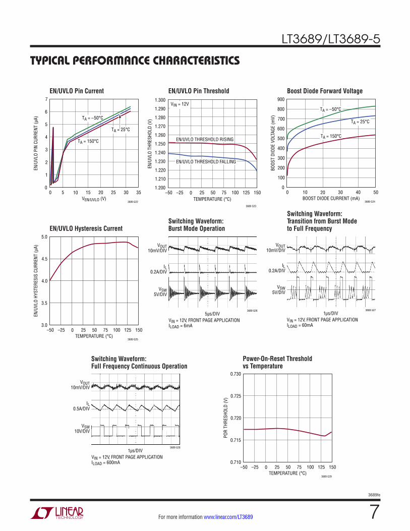
TYPICAL PERFORMANCE CHARACTERISTICS
EN/UVLO Pin Current EN/UVLO Pin Threshold Boost Diode Forward Voltage
EN/UVLO Hysteresis CurrentSwitching Waveform: Burst Mode Operation
Switching Waveform: Transition from Burst Mode to Full Frequency
Switching Waveform: Full Frequency Continuous Operation
Power-On-Reset Threshold vs Temperature
VEN/UVLO (V)
EN/U
VLO
PIN
CURR
ENT
(µA)
3689 G22
0 5 10 15 20 3025 35
6
7
5
4
1
0
3
2
TA = 150°C
TA = –50°C
TA = 25°C
TEMPERATURE (°C)–50
1.200
EN/U
VLO
THRE
SHOL
D (V
)
1.220
1.240
1.260
–25 0 25 50 10075 125
1.280
1.300
1.210
1.230
1.250
1.270
1.290
150
3689 G23
EN/UVLO THRESHOLD RISING
EN/UVLO THRESHOLD FALLING
VIN = 12V
BOOST DIODE CURRENT (mA)
BOOS
T DI
ODE
VOLT
AGE
(mV)
3689 G24
0 10 20 30 40 50
600
700
800
500
400
100
0
300
900
200
TA = 150°C
TA = 25°C
TA = –50°C
TEMPERATURE (°C)
3.0
EN/U
VLO
HYST
ERES
IS C
URRE
NT (µ
A)
3.5
4.0
4.5
5.0
3689 G25
–50 –25 0 25 50 10075 125 150
5µs/DIV
VOUT10mV/DIV
VIN = 12V, FRONT PAGE APPLICATIONILOAD = 6mA
VSW5V/DIV
IL0.2A/DIV
3689 G261µs/DIV
VOUT10mV/DIV
VIN = 12V, FRONT PAGE APPLICATIONILOAD = 60mA
VSW5V/DIV
IL0.2A/DIV
3689 G27
1µs/DIV
VOUT10mV/DIV
VIN = 12V, FRONT PAGE APPLICATIONILOAD = 600mA
VSW10V/DIV
IL0.5A/DIV
3689 G28
TEMPERATURE (°C)
0.710
POR
THRE
SHOL
D (V
)
0.715
0.720
0.725
0.730
3689 G29
–50 –25 0 25 50 10075 125 150
LT3689/LT3689-5
83689fe
For more information www.linear.com/LT3689
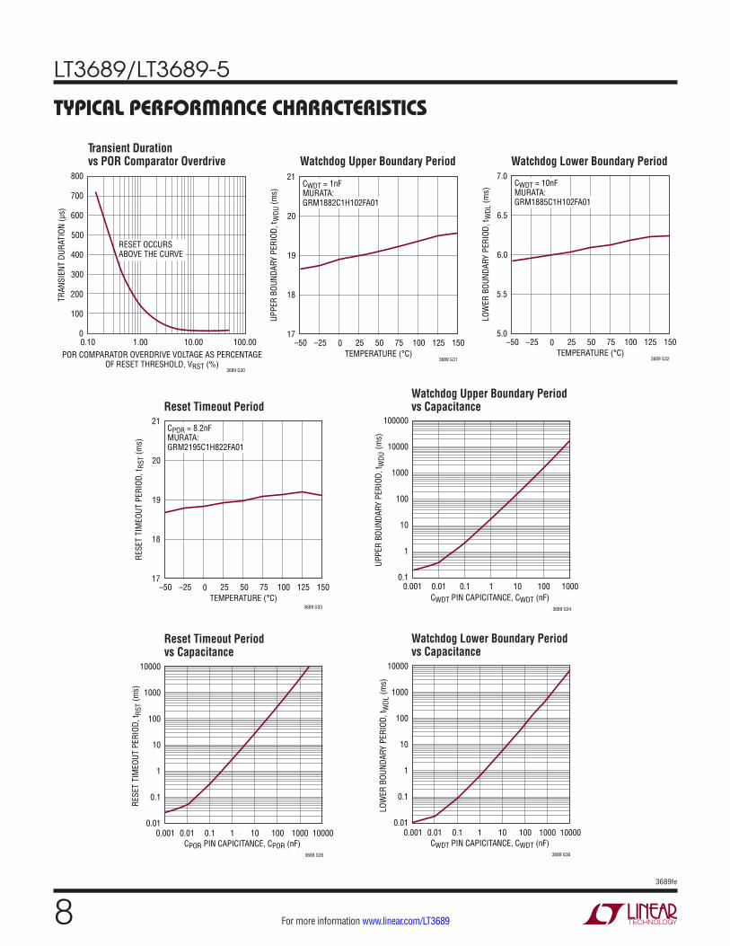
TYPICAL PERFORMANCE CHARACTERISTICS
Watchdog Upper Boundary Period Watchdog Lower Boundary Period
Reset Timeout PeriodWatchdog Upper Boundary Period vs Capacitance
Reset Timeout Period vs Capacitance
Transient Duration vs POR Comparator Overdrive
POR COMPARATOR OVERDRIVE VOLTAGE AS PERCENTAGEOF RESET THRESHOLD, VRST (%)
0.10
400
TRAN
SIEN
T DU
RATI
ON (µ
s)
500
600
700
800
1.00 10.00 100.00
300
200
100
0
3689 G30
RESET OCCURSABOVE THE CURVE
TEMPERATURE (°C)
17
UPPE
R BO
UNDA
RY P
ERIO
D, t W
DU (m
s)
18
19
20
21
3689 G31
–50 –25 0 25 50 10075 125 150
CWDT = 1nFMURATA:GRM1882C1H102FA01
TEMPERATURE (°C)
5.0
LOW
ER B
OUND
ARY
PERI
OD, t
WDL
(ms)
5.5
6.0
6.5
7.0
3689 G32
–50 –25 0 25 50 10075 125 150
CWDT = 10nFMURATA:GRM1885C1H102FA01
TEMPERATURE (°C)
17
RESE
T TI
MEO
UT P
ERIO
D, t R
ST (m
s)
18
19
20
21
3689 G33
–50 –25 0 25 50 10075 125 150
CPOR = 8.2nFMURATA:GRM2195C1H822FA01
0.001 0.01 0.1 1 10 100 1000CWDT PIN CAPICITANCE, CWDT (nF)
UPPE
R BO
UNDA
RY P
ERIO
D, t W
DU (m
s)
3689 G34
100
10000
0.1
1
100000
1000
10
CPOR PIN CAPICITANCE, CPOR (nF)
RESE
T TI
MEO
UT P
ERIO
D, t R
ST (m
s)
3689 G35
10
1000
0.01
0.1
10000
100
1
0.001 0.01 0.1 1 10 100 1000 10000
Watchdog Lower Boundary Period vs Capacitance
CWDT PIN CAPICITANCE, CWDT (nF)
LOW
ER B
OUND
ARY
PERI
OD, t
WDL
(ms)
3689 G36
10
1000
0.01
0.1
10000
100
1
0.001 0.01 0.1 1 10 100 1000 10000
LT3689/LT3689-5
93689fe
For more information www.linear.com/LT3689
PIN FUNCTIONSBST: The BST pin is used to provide drive voltage higher than the input voltage to the internal NPN power switch.
VIN: The VIN pin supplies current to the LT3689’s internal circuitry and to the internal power switch and must be locally bypassed.
SW: The SW pin is the output of the internal power switch. Connect this pin to the inductor, catch diode and boost capacitor.
DA: Tie the DA pin to the anode of the external catch Schottky diode. If the DA pin current exceeds 1.2A, which could occur in an overload or short-circuit condi- tion, switching is disabled until the DA pin current falls below 1.2A.
EN/UVLO: The EN/UVLO pin is used to put the LT3689 in shutdown mode. Pull the pin below 0.3V to shut down the LT3689. The 1.26V threshold can function as an accurate undervoltage lockout (UVLO), preventing the regulator from operating until the input voltage has reached the programmed level.
FB: The LT3689 regulates the feedback pin to 0.800V. Con-nect the feedback resistor divider tap to this pin. For the fixed LT3689-5 output, this pin can be used to connect a phase lead capacitor between the OUT pin and FB pin to optimize transient response.
WDE : Watchdog Timer Enable Pin. This pin disables the watchdog timer if the WDE voltage exceeds 1V. WDO is high in this condition.
W/T: Setting W/T low puts the LT3689 watchdog timer into window mode. If two or more negative edges occur on WDI before the watchdog lower boundary (tWDL) period expires, or no negative edge occurs within the watchdog upper boundary (tWDU) period, the part will set WDO low. If W/T is set high, the part will only set WDO low if no transi-tion occurs within the watchdog upper boundary period.
WDI: Watchdog Timer Input Pin. This pin receives the watchdog signal from a microprocessor. If the appropriate signal is not received, the part will pulse WDO low for a period equal to the reset timeout period. The watchdog timer is disabled until the WDO pin goes high again.
RST: Active low, open collector logic output with a weak pull-up to VOUT. After VOUT rises above 90% of its pro-grammed value, the reset remains asserted for the period set by the capacitor on the CPOR pin.
WDO: Active low, open collector logic output with weak pull-up to VOUT. WDO pulls low if the WDE is enabled and the microprocessor fails to drive the WDI pin of the LT3689 with an appropriate signal.
CWDT: Watchdog Timer Programming Pin. Place a capa-citor (CWDT) between this pin and ground to adjust the watchdog upper and lower boundary period. To determine the watchdog upper boundary period, and the lower bound-ary period, use the following equations:
tWDU = 18.2 • CWDT (watchdog upper boundary period)
tWDL = 0.588 • CWDT (watchdog lower boundary period)
tWDU and tWDL are in ms and CWDT is in nF. As an example, a 47nF capacitor will generate an 855ms watchdog upper boundary period and a 27.6ms watchdog lower boundary period.
CPOR: Reset Delay Timer Programming Pin. Attach an external capacitor (CPOR) to GND to set a reset delay time of 2.3ms/nF.
RT: Sets the Internal Oscillator Frequency. Tie a 31.6k resistor from RT to GND for a 500kHz switching frequency.
SYNC: Drive the SYNC pin with a logic level signal with positive and negative pulse widths of at least 80ns. The RT resistor should be chosen to set the LT3689 switching frequency at least 20% below the lowest synchronization input frequency.
OUT: The OUT pin supplies current to the internal circuitry when OUT is above 3V, reducing input quiescent current. The internal Schottky diode is connected from OUT to BST, providing the charging path for the boost capacitor. For the LT3689-5, this pin connects to the internal feedback divider that programs the fixed 5V output.
GND: Ground. Tie the exposed pad directly to the ground plane. The exposed pad metal of the package provides both electrical contact to ground and good thermal contact to the printed circuit board. The device must be soldered to the circuit board for proper operation.

LT3689/LT3689-5
103689fe
For more information www.linear.com/LT3689
BLOCK DIAGRAM
+–
+–
OSCILLATOR
TRANSITIONDETECT
WATCHDOGTIMER
ADJUSTABLERESET PULSEGENERATOR
Burst ModeOPERATION
DETECT
VC CLAMP
SOFT-START
INTERNAL0.8VREF
SLOPE COMP
R
VINVIN
VOUT
EN/UVLO
RT
BST
SW
SWITCHLATCH
GND
VOUT
C3
L1
D1
DISABLE
OUT
SYNC
ERROR AMP
OUT
RT
C1
FB
FB
80mV
VIN
3.4V
RSEN
2µA
2µA
22µA
22µA
1µA
1µA
SQ
Σ
DA
C2
R1
R2
OUT
525k
LT3689-5ONLY
100k
–
+
–
+
CWDT
WDI
RC
VC
CC
OUT
RST
CPOR
+
WDE
WDO
W/T
3689 BD
LT3689/LT3689-5
113689fe
For more information www.linear.com/LT3689
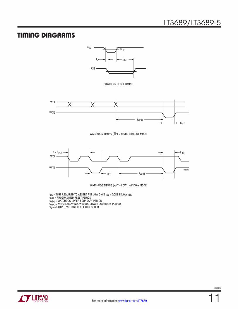
TIMING DIAGRAMS
3689 TD
tRST
tWDU
tWDU
t < tWDL
tRST
tRST
tRST
tUV
VOUT
POWER-ON RESET TIMING
WATCHDOG TIMING (W/T = HIGH), TIMEOUT MODE
VUV
WDO
WDI
WDI
WDO
RST
WATCHDOG TIMING (W/T = LOW), WINDOW MODE
tUV = TIME REQUIRED TO ASSERT RST LOW ONCE VOUT GOES BELOW VUVtRST = PROGRAMMED RESET PERIODtWDU = WATCHDOG UPPER BOUNDARY PERIODtWDL = WATCHDOG WINDOW MODE LOWER BOUNDARY PERIODVUV = OUTPUT VOLTAGE RESET THRESHOLD
LT3689/LT3689-5
123689fe
For more information www.linear.com/LT3689
OPERATIONThe LT3689 is a constant-frequency, current mode step-down regulator with a watchdog and a reset timer that allows microprocessor supervisory functions. Operation can be best understood by referring to the Block Diagram. Keeping the EN/UVLO pin at ground completely shuts off the part drawing minimal current from the VIN source. To turn on the internal bandgap and the rest of the logic cir-cuitry, raise the EN/UVLO pin above the accurate threshold of 1.26V. Also, VIN needs to be higher than 3.7V for the part to start switching.
Switching Regulator Operation
An oscillator, with frequency set by RT, enables an RS flip-flop, turning on the internal power switch. An amplifier and comparator monitor the current flowing between the VIN and SW pins, turning the switch off when this current reaches a level determined by the voltage at VC. An error amplifier measures the output voltage through the resistor divider tied to the FB pin and servos the VC voltage. If the error amplifier’s output increases, more current is delivered to the output; if it decreases, less current is delivered. An active clamp on the VC voltage provides current limit.
An internal regulator provides power to the control circuitry. The bias regulator normally draws current from the VIN pin, but if the OUT pin is connected to an external volt-age higher than 3V, bias current will be drawn from the external source (typically the regulated output voltage). This improves efficiency. The OUT pin also provides a cur-rent path to the internal boost diode that charges up the boost capacitor. The switch driver operates either from the VIN or from the BST pin. An external capacitor is used to generate a voltage at the BST pin that is higher than the VIN supply. This allows the driver to fully saturate the internal bipolar NPN power switch for efficient operation. To further optimize efficiency, the LT3689 automatically switches to Burst Mode operation in light load situations. Between bursts, all circuitry associated with controlling the output switch is shut down, reducing the input supply current to 85µA in a typical application. The oscillator reduces the LT3689’s operating frequency when the voltage at the FB pin is low. This frequency foldback helps to control the output current during start-up and overload conditions.
A comparator monitors the current flowing through the catch diode via the DA pin. This comparator delays switch-ing if the diode current goes higher than 1.2A (typical) during a fault condition such as a shorted output with high input voltage. The switching will only resume once the diode current has fallen below the 1.2A limit. This way the DA comparator regulates the valley current of the inductor to 1.2A during a short-circuit.
The LT3689 has an overvoltage protection feature which disables switching when the VIN goes above 38V (typical) during transients. When switching is disabled, the LT3689 can safely sustain transient input voltages up to 60V.
Power-On Reset and Watchdog Timer Operation
The LT3689 has a power-on reset (POR) comparator that monitors the regulated output voltage. If the output volt-age is below 10% of the regulation value, the RST pin is pulled low. Once the output voltage crosses over 90% of the regulation value, a reset timer is started and RST is released after the programmed reset delay time. The reset delay is programmable through the CPOR pin.
The watchdog typically monitors a microprocessor’s activ-ity. The watchdog can be enabled or disabled by applying a logic signal to the WDE pin. The watchdog can be oper-ated in either timeout or window mode by applying a logic signal to the W/T pin. In timeout mode, the microprocessor is required to change the logic state of the WDI pin on a periodic basis in order to clear the watchdog timer and to prevent the WDO from going low. In window mode, the watchdog timer requires successive negative edges on the WDI pin to come within a programmed time window to keep WDO from going low. Therefore, in window mode, if the time between the two negative WDI edges is too short or too long, then the WDO pin will be pulled low. When the WDO pin goes low, either in timeout or in window mode, the reset timer turns on and keeps the WDO pin low. The WDO pin will go high again once the reset timer expires or the RST pin goes low when the output voltage falls 10% below the regulation value. Both the timeout and window periods can be set through the CWDT pin.
LT3689/LT3689-5
133689fe
For more information www.linear.com/LT3689
The output voltage is programmed with a resistor divider between the output and the FB pin. Choose 1% resistors according to:
R1=R2
VOUT0.8V
1
For reference designators, refer to the Block Diagram.
Setting the Switching Frequency
The LT3689 uses a constant-frequency PWM architecture that can be programmed to switch from 350kHz to 2.2MHz by using a resistor tied from the RT pin to ground. Table 1 shows the RT values for various switching frequencies.
Table 1. Switching Frequency vs RT
SWITCHING FREQUENCY (MHz) RT (kΩ)
0.35 48.7
0.5 31.6
0.6 24.9
0.7 20.5
0.8 16.9
0.9 14.7
1 12.7
1.2 9.53
1.4 7.5
1.6 6.04
1.8 4.87
2 4.02
2.2 3.16
APPLICATIONS INFORMATIONOperating Frequency Trade-Offs
Selection of the operating frequency is a trade-off be-tween efficiency, component size and maximum input voltage. The advantage of high frequency operation is that smaller inductor and capacitor values may be used. The disadvantages are lower efficiency, and narrower input voltage range at constant-frequency. The highest constant-switching frequency (fSW(MAX)) for a given ap-plication can be calculated as follows:
fSW(MAX) = VOUT + VD
tON(MIN) VIN – VSW + VD( )where VIN is the typical input voltage, VOUT is the output voltage, VD is the catch diode drop (~0.5V) and VSW is the internal switch drop (~0.5V at maximum load). If the LT3689 is programmed to operate at a frequency higher than fSW(MAX) for a given VIN input voltage, the LT3689 enters pulse-skipping mode, where it skips switching cycles to maintain regulation. At frequencies higher than fSW(MAX), the LT3689 no longer operates with constant-frequency. The LT3689 enters pulse-skipping mode at frequencies higher than fSW(MAX) because of the limita-tion on the LT3689’s minimum on-time of 130ns. As the switching frequency is increased above fSW(MAX), the part is required to switch for shorter periods of time to maintain the same duty cycle. Delays associated with turning off the power switch dictate the minimum on-time of the part. When the required on-time decreases below the minimum on-time of 130ns, the switch pulse width remains fixed at 130ns (instead of becoming narrower to accommodate the duty cycle requirement). The inductor current ramps up to a value exceeding the load current and the output ripple increases. The part then remains off until the output voltage dips below the programmed value before it begins switching again.
LT3689/LT3689-5
143689fe
For more information www.linear.com/LT3689
Maximum Operating Voltage
The maximum input voltage for LT3689 applications depends on switching frequency, the absolute maximum ratings of the VIN and BST pins, and by the minimum duty cycle (DCMIN). The LT3689 can operate from input voltages up to 36V, and safely withstand input transient voltages up to 60V. Note that while VIN > 38V (typical), the LT3689 will stop switching, allowing the output to fall out of regulation.
DCMIN = tON(MIN) • fSW
where tON(MIN) is equal to 130ns (for TJ > 125°C tON(MIN) is equal to 150ns) and fSW is the switching frequency. Running at a lower switching frequency allows a lower minimum duty cycle. The maximum input voltage before pulse-skipping occurs depends on the output voltage and the minimum duty cycle:
VIN(PS) = VOUT + VD
DCMIN– VD + VSW
Example: fSW = 790kHz, VOUT = 3.3V, DCMIN = 130ns • 790kHz = 0.103
VIN(PS) = 3.3V + 0.4V
0.103– 0.4V + 0.4V = 36V
The LT3689 will regulate the output current at input volt-ages greater than VIN(PS). For example, an application
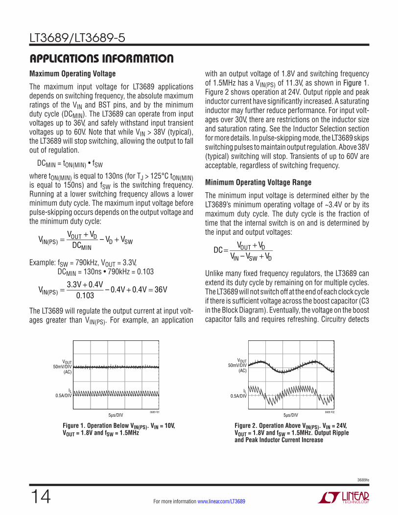
with an output voltage of 1.8V and switching frequency of 1.5MHz has a VIN(PS) of 11.3V, as shown in Figure 1. Figure 2 shows operation at 24V. Output ripple and peak inductor current have significantly increased. A saturating inductor may further reduce performance. For input volt-ages over 30V, there are restrictions on the inductor size and saturation rating. See the Inductor Selection section for more details. In pulse-skipping mode, the LT3689 skips switching pulses to maintain output regulation. Above 38V (typical) switching will stop. Transients of up to 60V are acceptable, regardless of switching frequency.
Minimum Operating Voltage Range
The minimum input voltage is determined either by the LT3689’s minimum operating voltage of ~3.4V or by its maximum duty cycle. The duty cycle is the fraction of time that the internal switch is on and is determined by the input and output voltages:
DC = VOUT + VD
VIN – VSW + VD
Unlike many fixed frequency regulators, the LT3689 can extend its duty cycle by remaining on for multiple cycles. The LT3689 will not switch off at the end of each clock cycle if there is sufficient voltage across the boost capacitor (C3 in the Block Diagram). Eventually, the voltage on the boost capacitor falls and requires refreshing. Circuitry detects
APPLICATIONS INFORMATION
Figure 1. Operation Below VIN(PS). VIN = 10V, VOUT = 1.8V and fSW = 1.5MHz
Figure 2. Operation Above VIN(PS). VIN = 24V, VOUT = 1.8V and fSW = 1.5MHz. Output Ripple and Peak Inductor Current Increase
5µs/DIV
VOUT50mV/DIV
(AC)
IL0.5A/DIV
3689 F015µs/DIV
VOUT50mV/DIV
(AC)
IL0.5A/DIV
3689 F02
LT3689/LT3689-5
153689fe
For more information www.linear.com/LT3689
this condition and forces the switch to turn off, allowing the inductor current to charge up the boost capacitor. This places a limitation on the maximum duty cycle. The maximum duty cycle that the LT3689 can sustain is 90%. From this DCMAX number, the minimum operating voltage can be calculated using the following equation:
VIN(MIN) = VOUT + VD
0.90− VD + VSW
Example: VOUT = 3.3V
VIN(MIN) = 3.3V + 0.4V
0.90– 0.4V + 0.4V = 4.1V
Inductor Selection and Maximum Output Current
A good first choice for the inductor value is:
L = (VOUT + VF ) •
2.2MHzfSW
where VF is the voltage drop of the catch diode (~0.4V), fSW is the switching frequency in MHz, and L is in µH. The inductor’s RMS current rating must be greater than the maximum load current and its saturation current should be at least 30% higher. For robust operation in fault con-ditions (start-up or short-circuit) and high input voltage (>30V), use an 8.2µH or greater inductor (for TJ > 125°C, use 10µH or larger) with a saturation rating of 2.5A, or
higher. To keep the efficiency high, the series resistance (DCR) should be less than 0.15Ω and the core mate-rial should be intended for high frequency applications. Table 2 lists several vendors and suitable types.
The current in the inductor is a triangle wave with an average value equal to the load current. The peak switch current is equal to the output current plus half the peak-to-peak inductor ripple current. The LT3689 limits its switch current in order to protect itself and the system from overload faults. Therefore, the maximum output current that the LT3689 will deliver depends on the switch current limit, the inductor value, and the input and output volt-ages. Also, if the inductor current’s bottom peak exceeds the DA current limit (ILIM(DA)) at high output currents then the DA current comparator will regulate the bottom peak to ILIM(DA). This will result in higher inductor ripple current and will further limit the max output current. The DA current limit consists of a DC and an AC component. The nominal DC component is fixed at 1.2A. The AC component depends on the output voltage, inductor size and a fixed time delay between the DA comparator turn-ing off and switch turning on. Therefore, the DA current limit ILIM(DA) will increase as the output voltage collapses under overload conditions.
ILIM(DA) = 1.2A −
VOUT + VD( )L
• 0.25µs
Table 2. Inductor Vendors VENDOR
URL
PART SERIES
INDUCTANCE RANGE (µH)
SIZE (mm)
Sumida www.sumida.com CDRH4D28 CDRH5D28
1.2 to 4.7 2.5 to 10
4.5 × 4.5 5.5 × 5.5
Toko www.toko.com A916CY D585LC
2 to 12 1.1 to 39
6.3 × 6.2 8.1 × 8
Würth Elektronik www.we-online.com WE-TPC(M) WE-PD2(M)
1 to 10 2.2 to 22
4.8 × 4.8 5.2 × 5.8
APPLICATIONS INFORMATION
LT3689/LT3689-5
163689fe
For more information www.linear.com/LT3689
Choose an inductor using the previous inductor selection equation to guarantee 700mA of output current. If using a smaller inductor, check the DA current limit equation to verify that the DA circuitry will not lower the switching frequency.
When the switch is off, the potential across the inductor is the output voltage plus the catch diode drop. This gives the peak-to-peak ripple current in the inductor:
∆IL = (1− DC)(VOUT + VD)
L • fSW
where fSW is the switching frequency of the LT3689 and L is the value of the inductor. The peak inductor and switch current is:
ISW(PK) = IL(PK) = IOUT + ∆IL
2
To maintain output regulation, this peak current must be less than the LT3689’s switch current limit ILIM. ILIM is at least 1.5A for at low duty cycles and decreases linearly to 0.87A at DC = 85%. The maximum output current is a function of the chosen inductor value.
IOUT(MAX) = ILIM − ∆IL2
= 1.15A • (1− 0.28 • DC) − ∆IL2
Choosing an inductor value so that the ripple current is small will allow a maximum output current near the switch current limit.
One approach to choosing the inductor is to start with the preceding simple rule, determine the available inductors, and choose one to meet cost or space goals. Next, use these equations to check that the LT3689 will be able to deliver the required output current. Note again that these equations assume that the inductor current is continu-ous. Discontinuous operation occurs when IOUT is less than ∆IL /2.
Of course, such a simple design guide will not always result in the optimum inductor for the application. A larger value inductor provides a slightly higher maximum load current and will reduce the output voltage ripple. If the
load is lower than 0.7A, decrease the value of the inductor and operate with a higher ripple current. This allows the use of a physically smaller inductor, or one with a lower DCR resulting in higher efficiency. There are graphs in the Typical Performance Characteristics section of this data sheet that show the maximum load current as a function of input voltage for several popular output volt-ages. Low inductance may result in discontinuous mode operation, which is okay but further reduces maximum load current. For details of maximum output current and discontinuous mode operation, see Linear Technology Application Note 44. Finally, for duty cycles greater than 50% (VOUT/ VIN > 0.5), a minimum inductance is required to avoid subharmonic oscillations:
LMIN =
1.4 VOUT + VD( )fSW
where LMIN is in µH, VOUT and VD are in volts, and fSW is in MHz.
Input Capacitor
Bypass the input of the LT3689 circuit with a ceramic capacitor of an X7R or X5R type. Y5V types have poor performance over temperature and applied voltage, and should not be used. The minimum value of input capaci-tance depends on the switching frequency. Use an input capacitor of 1µF or more for switching frequencies be- tween 1MHz to 2.2MHz, and 2.2µF or more for frequen-cies lower than 1MHz. If the input power source has high impedance, or there is significant inductance due to long wires or cables, additional bulk capacitance may be nec-essary. This can be provided with a lower performance electrolytic capacitor. Step-down regulators draw current from the input supply in pulses with very fast rise and fall times. The input capacitor is required to reduce the resulting voltage ripple at the LT3689 input and to force this very high frequency switching current into a tight local loop, minimizing EMI. A ceramic capacitor is capable of this task, but only if it is placed close to the LT3689 and the catch diode (see the PCB Layout section). A second precaution regarding the ceramic input capacitor concerns the maximum input voltage rating of the LT3689. A ceramic input capacitor combined with trace or cable inductance forms a high quality (under damped) tank circuit. If the
APPLICATIONS INFORMATION
LT3689/LT3689-5
173689fe
For more information www.linear.com/LT3689
LT3689 circuit is plugged into a live supply, the input volt-age can ring to twice its nominal value, possibly exceeding the LT3689’s voltage rating. For a complete discussion, see Linear Technology’s Application Note 88.
Output Capacitor and Output Ripple
The output capacitor has two essential functions. Along with the inductor, it filters the square wave generated by the LT3689 to produce the DC output. In this role it determines the output ripple, and low impedance at the switching frequency is important. The second function is to store energy in order to satisfy transient loads and stabilize the LT3689’s control loop. Ceramic capacitors have very low equivalent series resistance (ESR) and provide the best ripple performance. A good starting value is:
COUT = 50
VOUT fSW
where fSW is in MHz, and COUT is the recommended out-put capacitance in µF. Use X5R or X7R types, which will provide low output ripple and good transient response. Transient performance can be improved with a high value capacitor, but a phase lead capacitor across the feedback resistor R1 may be required to get the full benefit (see the Frequency Compensation section).
High performance electrolytic capacitors can be used for the output capacitor. Low ESR is important, so choose one that is intended for use in switching regulators. The ESR should be specified by the supplier and should be 0.1Ω or less. Such a capacitor will be larger than a ceramic capacitor and will have a larger capacitance because the
capacitor must be large to achieve low ESR. Table 3 lists several capacitor vendors.
Table 3. Capacitor VendorsVENDOR PHONE URL
Panasonic (714) 373-7366 www.panasonic.com
Kemet (864) 963-6300 www.kemet.com
Sanyo (408) 749-9714 www.sanyovideo.com
Murata (408) 436-1300 www.murata.com
AVX www.avxcorp.com
Taiyo Yuden (864) 963-6300 www.taiyo-yuden.com
Catch Diode
The catch diode conducts current only during switch-off time. Average forward current in normal operation can be calculated from:
ID(AVG) =
IOUT (VIN − VOUT )
VIN
where IOUT is the output load current. The only reason to consider a diode with a larger current rating than neces-sary for nominal operation is for the worst-case condition of shorted output. The diode current will then increase to the typical peak switch current limit. Peak reverse voltage is equal to the regulator input voltage. Use a Schottky diode with a reverse voltage rating greater than the input voltage. The overvoltage protection feature in the LT3689 will keep the switch off when VIN > 38V (typical), which allows the use of a 40V rated Schottky even when VIN ranges up to 60V. Table 4 lists several Schottky diodes and their manufacturers.
APPLICATIONS INFORMATION
LT3689/LT3689-5
183689fe
For more information www.linear.com/LT3689
Table 4. Diode Vendors PART NUMBER
VR (V)
IAVE (A)
VF AT IAVE (mV)
On Semiconductor MBRM120E MBRM140
20 40
1 1
530 550
Diodes Inc. B120 B130 B140 B0540W B140HB
20 30 40 40 40
1 1 1
0.5 1
500 500 500 510 530
Ceramic Capacitors
Ceramic capacitors are small, robust and have very low ESR. However, ceramic capacitors can cause problems when used with the LT3689 due to their piezoelectric nature. When in Burst Mode operation, the LT3689’s switching frequency depends on the load current, and at very light loads the LT3689 can excite the ceramic capaci-tor at audio frequencies, generating audible noise. Since the LT3689 operates at a lower current limit during Burst Mode operation, the noise is typically very quiet. If this noise is unacceptable, use a high performance tantalum or electrolytic capacitor at the output.
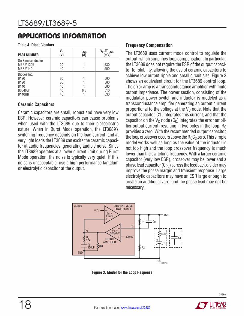
Frequency Compensation
The LT3689 uses current mode control to regulate the output, which simplifies loop compensation. In particular, the LT3689 does not require the ESR of the output capaci-tor for stability, allowing the use of ceramic capacitors to achieve low output ripple and small circuit size. Figure 3 shows an equivalent circuit for the LT3689 control loop. The error amp is a transconductance amplifier with finite output impedance. The power section, consisting of the modulator, power switch and inductor, is modeled as a transconductance amplifier generating an output current proportional to the voltage at the VC node. Note that the output capacitor, C1, integrates this current, and that the capacitor on the VC node (CC) integrates the error ampli-fier output current, resulting in two poles in the loop. RC provides a zero. With the recommended output capacitor, the loop crossover occurs above the RCCC zero. This simple model works well as long as the value of the inductor is not too high and the loop crossover frequency is much lower than the switching frequency. With a larger ceramic capacitor (very low ESR), crossover may be lower and a phase lead capacitor (CPL) across the feedback divider may improve the phase margin and transient response. Large electrolytic capacitors may have an ESR large enough to create an additional zero, and the phase lead may not be necessary.
APPLICATIONS INFORMATION
Figure 3. Model for the Loop Response
–
+
–
+
800mV
VC
LT3689
GND
3689 F03
R1
OUT
ESR
ERRORAMPLIFIER
CURRENT MODEPOWER STAGE
FB
R23M
RC37k
CC100pF
C1
C1
gm =300µA/V
gm =1.2A/V
+
CPL
0.7V
LT3689/LT3689-5
193689fe
For more information www.linear.com/LT3689
Most applications running at VIN greater than 20V will require a small phase lead capacitor, ranging from 2pF to about 30pF, between the FB pin and VOUT for good transient response. The circuits in the Typical Applications section use the appropriate phase lead capacitors and are stable at all input voltages.
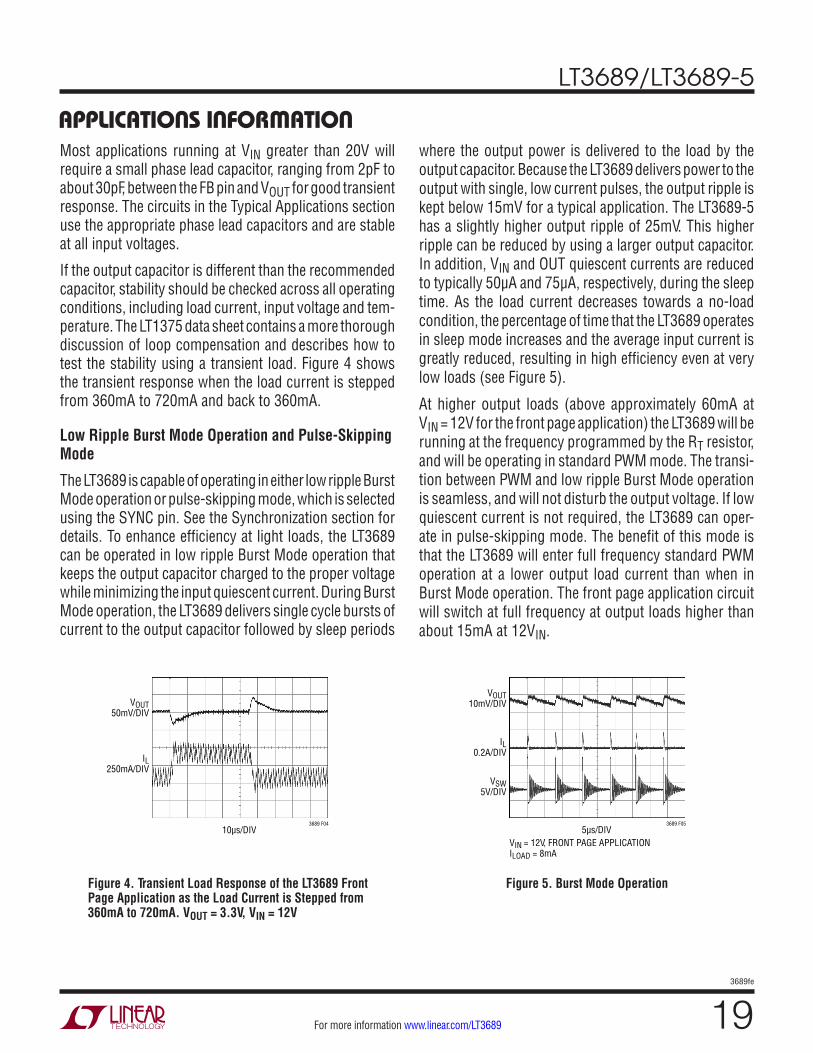
If the output capacitor is different than the recommended capacitor, stability should be checked across all operating conditions, including load current, input voltage and tem-perature. The LT1375 data sheet contains a more thorough discussion of loop compensation and describes how to test the stability using a transient load. Figure 4 shows the transient response when the load current is stepped from 360mA to 720mA and back to 360mA.
Low Ripple Burst Mode Operation and Pulse-Skipping Mode
The LT3689 is capable of operating in either low ripple Burst Mode operation or pulse-skipping mode, which is selected using the SYNC pin. See the Synchronization section for details. To enhance efficiency at light loads, the LT3689 can be operated in low ripple Burst Mode operation that keeps the output capacitor charged to the proper voltage while minimizing the input quiescent current. During Burst Mode operation, the LT3689 delivers single cycle bursts of current to the output capacitor followed by sleep periods
where the output power is delivered to the load by the output capacitor. Because the LT3689 delivers power to the output with single, low current pulses, the output ripple is kept below 15mV for a typical application. The LT3689-5 has a slightly higher output ripple of 25mV. This higher ripple can be reduced by using a larger output capacitor. In addition, VIN and OUT quiescent currents are reduced to typically 50µA and 75µA, respectively, during the sleep time. As the load current decreases towards a no-load condition, the percentage of time that the LT3689 operates in sleep mode increases and the average input current is greatly reduced, resulting in high efficiency even at very low loads (see Figure 5).
At higher output loads (above approximately 60mA at VIN = 12V for the front page application) the LT3689 will be running at the frequency programmed by the RT resistor, and will be operating in standard PWM mode. The transi-tion between PWM and low ripple Burst Mode operation is seamless, and will not disturb the output voltage. If low quiescent current is not required, the LT3689 can oper-ate in pulse-skipping mode. The benefit of this mode is that the LT3689 will enter full frequency standard PWM operation at a lower output load current than when in Burst Mode operation. The front page application circuit will switch at full frequency at output loads higher than about 15mA at 12VIN.
APPLICATIONS INFORMATION
Figure 4. Transient Load Response of the LT3689 Front Page Application as the Load Current is Stepped from 360mA to 720mA. VOUT = 3.3V, VIN = 12V
Figure 5. Burst Mode Operation
10µs/DIV
VOUT50mV/DIV
IL250mA/DIV
3689 F045µs/DIV
VOUT10mV/DIV
VIN = 12V, FRONT PAGE APPLICATIONILOAD = 8mA
VSW5V/DIV
IL0.2A/DIV
3689 F05
LT3689/LT3689-5
203689fe
For more information www.linear.com/LT3689
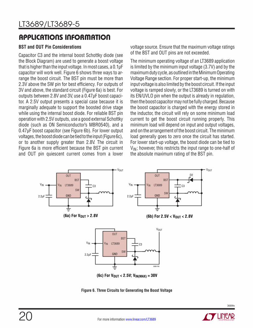
BST and OUT Pin Considerations
Capacitor C3 and the internal boost Schottky diode (see the Block Diagram) are used to generate a boost voltage that is higher than the input voltage. In most cases, a 0.1µF capacitor will work well. Figure 6 shows three ways to ar-range the boost circuit. The BST pin must be more than 2.3V above the SW pin for best efficiency. For outputs of 3V and above, the standard circuit (Figure 6a) is best. For outputs between 2.8V and 3V, use a 0.47µF boost capaci-tor. A 2.5V output presents a special case because it is marginally adequate to support the boosted drive stage while using the internal boost diode. For reliable BST pin operation with 2.5V outputs, use a good external Schottky diode (such as ON Semiconductor’s MBR0540), and a 0.47µF boost capacitor (see Figure 6b). For lower output voltages, the boost diode can be tied to the input (Figure 6c), or to another supply greater than 2.8V. The circuit in Figure 6a is more efficient because the BST pin current and OUT pin quiescent current comes from a lower
voltage source. Ensure that the maximum voltage ratings of the BST and OUT pins are not exceeded.
The minimum operating voltage of an LT3689 application is limited by the minimum input voltage (3.7V) and by the maximum duty cycle, as outlined in the Minimum Operating Voltage Range section. For proper start-up, the minimum input voltage is also limited by the boost circuit. If the input voltage is ramped slowly, or the LT3689 is turned on with its EN/UVLO pin when the output is already in regulation, then the boost capacitor may not be fully charged. Because the boost capacitor is charged with the energy stored in the inductor, the circuit will rely on some minimum load current to get the boost circuit running properly. This minimum load will depend on input and output voltages, and on the arrangement of the boost circuit. The minimum load generally goes to zero once the circuit has started. For lower start-up voltage, the boost diode can be tied to VIN; however, this restricts the input range to one-half of the absolute maximum rating of the BST pin.
APPLICATIONS INFORMATION
Figure 6. Three Circuits for Generating the Boost Voltage
VIN
BST
SW
OUT
VIN
VOUT
2.2µF
C3
GND
LT3689 VIN
BST
SW
OUT
VIN
VOUT
2.2µF
C3
D2
GND
LT3689
VIN
BST
SW
OUT
VIN
VOUT
2.2µF
C3
GND
LT3689
3689 F06
(6a) For VOUT > 2.8V (6b) For 2.5V < VOUT < 2.8V
(6c) For VOUT < 2.5V; VIN(MAX) = 30V
LT3689/LT3689-5
213689fe
For more information www.linear.com/LT3689
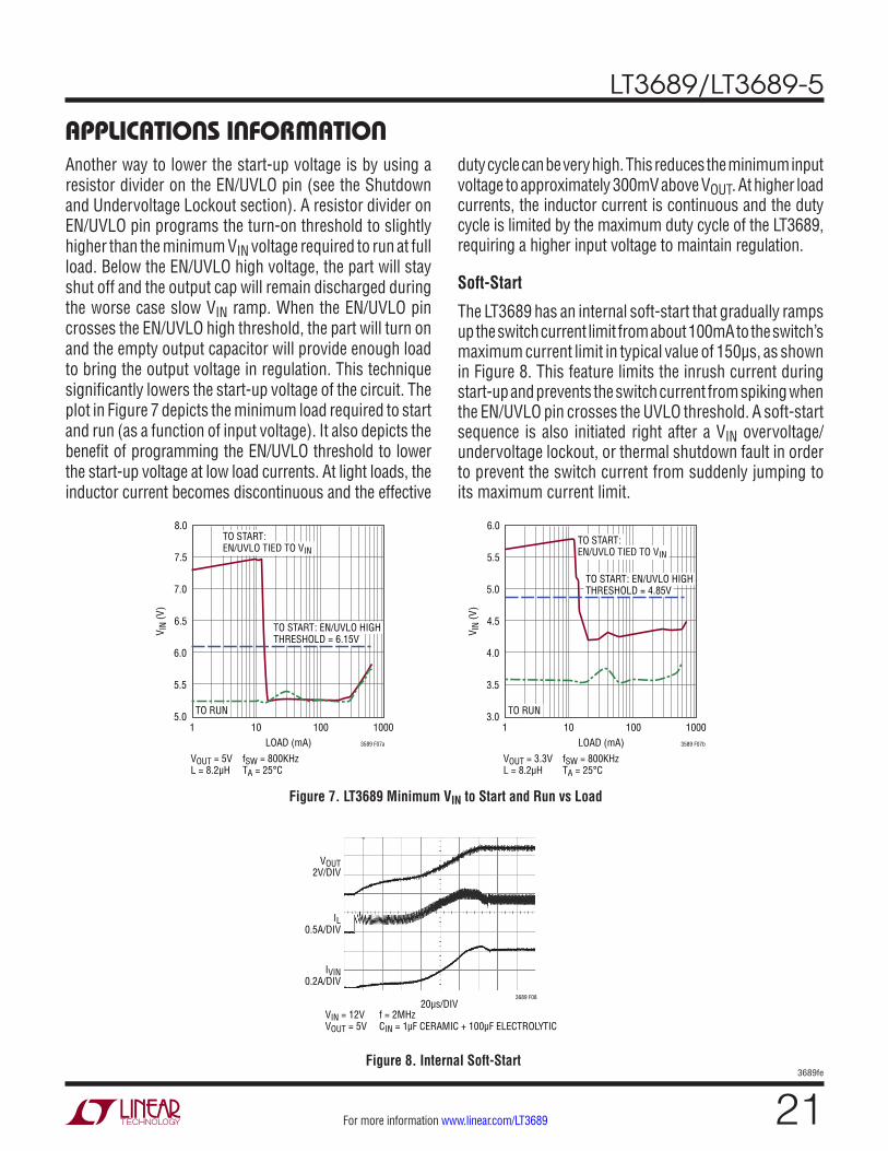
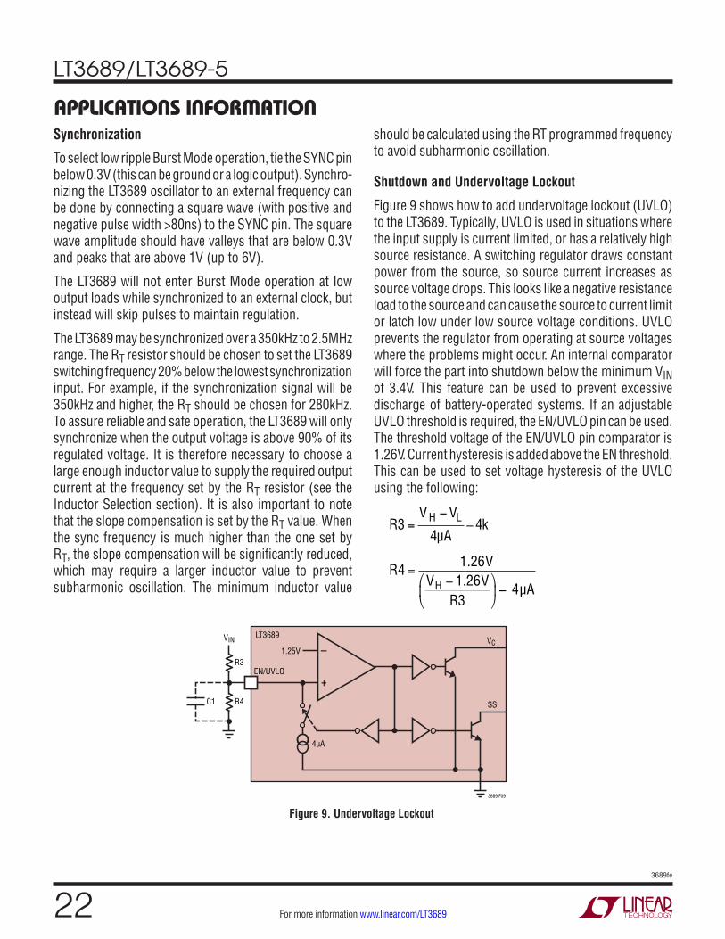
Another way to lower the start-up voltage is by using a resistor divider on the EN/UVLO pin (see the Shutdown and Undervoltage Lockout section). A resistor divider on EN/UVLO pin programs the turn-on threshold to slightly higher than the minimum VIN voltage required to run at full load. Below the EN/UVLO high voltage, the part will stay shut off and the output cap will remain discharged during the worse case slow VIN ramp. When the EN/UVLO pin crosses the EN/UVLO high threshold, the part will turn on and the empty output capacitor will provide enough load to bring the output voltage in regulation. This technique significantly lowers the start-up voltage of the circuit. The plot in Figure 7 depicts the minimum load required to start and run (as a function of input voltage). It also depicts the benefit of programming the EN/UVLO threshold to lower the start-up voltage at low load currents. At light loads, the inductor current becomes discontinuous and the effective
duty cycle can be very high. This reduces the minimum input voltage to approximately 300mV above VOUT. At higher load currents, the inductor current is continuous and the duty cycle is limited by the maximum duty cycle of the LT3689, requiring a higher input voltage to maintain regulation.
Soft-Start
The LT3689 has an internal soft-start that gradually ramps up the switch current limit from about 100mA to the switch’s maximum current limit in typical value of 150µs, as shown in Figure 8. This feature limits the inrush current during start-up and prevents the switch current from spiking when the EN/UVLO pin crosses the UVLO threshold. A soft-start sequence is also initiated right after a VIN overvoltage/undervoltage lockout, or thermal shutdown fault in order to prevent the switch current from suddenly jumping to its maximum current limit.
APPLICATIONS INFORMATION
Figure 7. LT3689 Minimum VIN to Start and Run vs Load
Figure 8. Internal Soft-Start
20µs/DIV
VOUT2V/DIV
VIN = 12VVOUT = 5V
f = 2MHzCIN = 1µF CERAMIC + 100µF ELECTROLYTIC
IVIN0.2A/DIV
IL0.5A/DIV
3689 F08
LOAD (mA)1
7.0
V IN
(V)
7.5
10 100 1000
6.5
6.0
5.5
5.0
8.0
3589 F07a
TO START: EN/UVLO TIED TO VIN
TO RUN
VOUT = 5VL = 8.2µH
fSW = 800KHzTA = 25°C
TO START: EN/UVLO HIGHTHRESHOLD = 6.15V
LOAD (mA)1
5.0
V IN
(V)
5.5
10 100 1000
4.5
4.0
3.5
3.0
6.0
3589 F07b
TO START: EN/UVLO TIED TO VIN
TO RUN
VOUT = 3.3VL = 8.2µH
fSW = 800KHzTA = 25°C
TO START: EN/UVLO HIGHTHRESHOLD = 4.85V
LT3689/LT3689-5
223689fe
For more information www.linear.com/LT3689
Synchronization
To select low ripple Burst Mode operation, tie the SYNC pin below 0.3V (this can be ground or a logic output). Synchro-nizing the LT3689 oscillator to an external frequency can be done by connecting a square wave (with positive and negative pulse width >80ns) to the SYNC pin. The square wave amplitude should have valleys that are below 0.3V and peaks that are above 1V (up to 6V).
The LT3689 will not enter Burst Mode operation at low output loads while synchronized to an external clock, but instead will skip pulses to maintain regulation.
The LT3689 may be synchronized over a 350kHz to 2.5MHz range. The RT resistor should be chosen to set the LT3689 switching frequency 20% below the lowest synchronization input. For example, if the synchronization signal will be 350kHz and higher, the RT should be chosen for 280kHz. To assure reliable and safe operation, the LT3689 will only synchronize when the output voltage is above 90% of its regulated voltage. It is therefore necessary to choose a large enough inductor value to supply the required output current at the frequency set by the RT resistor (see the Inductor Selection section). It is also important to note that the slope compensation is set by the RT value. When the sync frequency is much higher than the one set by RT, the slope compensation will be significantly reduced, which may require a larger inductor value to prevent subharmonic oscillation. The minimum inductor value
should be calculated using the RT programmed frequency to avoid subharmonic oscillation.
Shutdown and Undervoltage Lockout
Figure 9 shows how to add undervoltage lockout (UVLO) to the LT3689. Typically, UVLO is used in situations where the input supply is current limited, or has a relatively high source resistance. A switching regulator draws constant power from the source, so source current increases as source voltage drops. This looks like a negative resistance load to the source and can cause the source to current limit or latch low under low source voltage conditions. UVLO prevents the regulator from operating at source voltages where the problems might occur. An internal comparator will force the part into shutdown below the minimum VIN of 3.4V. This feature can be used to prevent excessive discharge of battery-operated systems. If an adjustable UVLO threshold is required, the EN/UVLO pin can be used. The threshold voltage of the EN/UVLO pin comparator is 1.26V. Current hysteresis is added above the EN threshold. This can be used to set voltage hysteresis of the UVLO using the following:
R3 =V H VL
4µA4k
R4 = 1.26VVH 1.26V
R34µA
APPLICATIONS INFORMATION
Figure 9. Undervoltage Lockout
1.25V
4µA
R3
R4C1
EN/UVLO
LT3689VIN
SS
VC
3689 F09
–
+
LT3689/LT3689-5
233689fe
For more information www.linear.com/LT3689
Example: switching should not start until the input is above 4.40V, and is to stop if the input falls below 4V.
V H = 4.40V,VL = 4V
R3 = 4.40V − 4V4µA
− 4k = 95.3k
R4 = 1.26V4.40V − 1.26V
95.3k– 4µA
= 43.2k(Nearest 1%Resistor)
Keep the connection from the resistor to the EN/UVLO pin short and make sure the interplane or surface capaci-tance to switching nodes is minimized. If high resistor values are used, the EN/UVLO pin should be bypassed with a 1nF capacitor to prevent coupling problems from the switch node.
Output Voltage Monitoring
The LT3689 provides power supply monitoring for micro-processor-based systems. The features include power-on reset (POR) and watchdog timing.
A precise internal voltage reference and glitch immune precision POR comparator circuit monitor the LT3689 output voltage. The switcher’s output voltage must be above 90% of programmed value for RST not to be asserted (refer to the Timing Diagram). The LT3689 will assert RST during power-up, power-down and brownout conditions. Once the output voltage rises above the RST threshold, the adjustable reset timer is started and RST is released after the reset timeout period. On power-down, once the output voltage drops below RST threshold, RST is held at a logic low. The reset timer is adjustable using external capacitors. The RST pin has a weak pull-up to the OUT pin.
The POR comparator is designed to be robust against FB pin noise, which could potentially false trigger the RST pin. The POR comparator lowpass filters the first stage of the comparator. This filter integrates the output of the compara-tor before asserting the RST. The benefit of adding this filter is that any transients at the buck regulator’s output must be of sufficient magnitude and duration before it triggers a logic change in the output (see the Typical Transient vs POR Comparator Overdrive in the Typical Performance
Characteristics section). This prevents spurious resets caused by output voltage transients such as load steps or short brownout conditions without sacrificing the DC reset threshold accuracy.
Watchdog
The LT3689 includes an adjustable watchdog timer that monitors a µP’s activity. If a code execution error occurs in a µP, the watchdog will detect this error and will set the WDO low. This signal can be used to interrupt a routine or to reset a microprocessor.
The watchdog is operated either in timeout or window mode. In timeout mode, the microprocessor needs to toggle the WDI pin before the watchdog timer expires, to keep the WDO pin high. If no WDI pulse (either positive or negative) appears during the programmed timeout period, then the circuitry will pull WDO low. During normal opera-tion, the WDI input signal’s high to low, and low to high transition periods should be set lower than the watchdog’s programmed time to keep WDO inactive.
In window mode, the watchdog circuitry is triggered by negative edges on the WDI pin. The window mode restricts the WDI pin’s negative going pulses to appear inside a programmed time window (see the Timing Diagram) to prevent WDO from going low. If more than two pulses are registered in the watchdog lower boundary period, the WDO is forced to go low. The WDI edges are ignored while the CWDT capacitor charges from 0V to 200mV right after a low to high transition on the WDO or RST pin. The WDO also goes low if no negative edge is supplied to the WDI pin in the watchdog upper boundary period. During a code execution error, the microprocessor will output WDI pulses that would be either too fast or too slow. This condition will assert WDO and force the microprocessor to reset the program. In window mode, the WDI signal frequency is bounded by an upper and lower limit for normal operation. The WDI input frequency period should be higher than the tWDL period, and lower than the tWDU period, to keep WDO high under normal conditions. The window mode’s tWDL and tWDU times have a fixed ratio of 31 between them. These times can be increased or decreased by adjusting an external capacitor on the CWDT pin.
APPLICATIONS INFORMATION
LT3689/LT3689-5
243689fe
For more information www.linear.com/LT3689
In both watchdog modes, when WDO is asserted, the reset timer is enabled. Any WDI pulses that appear while the reset timer is running are ignored. When the reset timer expires, the WDO is allowed to go high again. Therefore, if no input is applied to the WDI pin, then the watchdog circuitry produces a train of pulses on the WDO pin. The high time of this pulse train is equal to the timeout period, and low time is equal to the reset period. Also, WDO and RST cannot be logic low simultaneously. If WDO is low and RST goes low, then WDO will go high.
The WDE pin allows the user to turn on and off the watch-dog function. Do not leave this pin open. Tie it high or low to turn watchdog off or on, respectively. The W/T pin enables/disables the window/timeout mode. Leaving this pin open is fine and will put the watchdog in window mode. It has a weak pull-down to ground. The WDI pin has an internal 2µA weak pull-up that keeps the WDI pin high. If watchdog is disabled, leaving this pin open is acceptable.
Selecting the Reset Timing Capacitors
The reset timeout period is adjustable in order to accom-modate a variety of microprocessor applications. The reset timeout period, (tRST), is adjusted by connecting a capacitor, CPOR, between the CPOR pin and ground. The value of this capacitor is determined by:
CPOR = tRST • 432 pF
ms
This equation is accurate for reset timeout periods of 5ms, or greater. To program faster timeout periods, see the Reset Timeout Period vs Capacitance graph in the Typical Performance Characteristics section. Leaving the CPOR pin unconnected will generate a minimum reset timeout of approximately 25µs. Maximum reset timeout is limited by the largest available low leakage capacitor. The accuracy of the timeout period will be affected by
APPLICATIONS INFORMATION
Figure 10. Reset Timer Waveforms Figure 11. Window Watchdog Waveforms (W/T = Low)
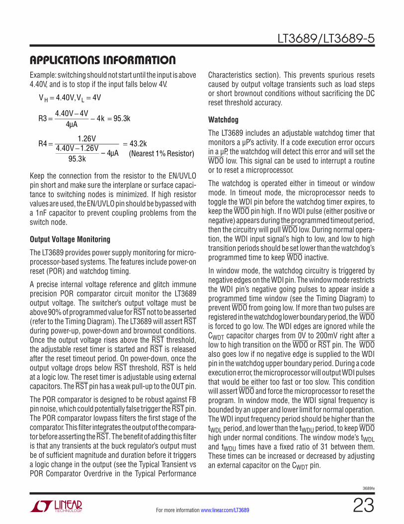
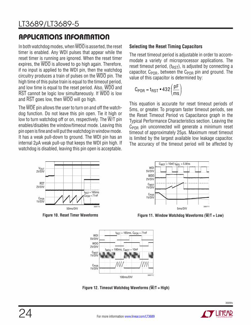
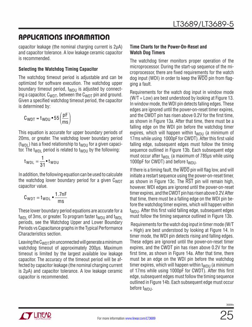
Figure 12. Timeout Watchdog Waveforms (W/T = High)
50ms/DIV
VOUT2V/DIV
CPOR1V/DIV
RST2V/DIV
3689 F10
tRST = 165msCPOR = 71nF
5ms/DIV
CWDT1V/DIV
CPOR1V/DIV
WDI5V/DIV
WDO2V/DIV
3689 F11
CWDT = 10nF, tWDL = 5.8ms
100ms/DIV
CWDT1V/DIV
CPOR1V/DIV
WDI5V/DIV
WDO2V/DIV
3689 F12
tRST = 165ms, CPOR = 71nF
tWDU = 180ms, CWDT = 10nF
LT3689/LT3689-5
253689fe
For more information www.linear.com/LT3689
capacitor leakage (the nominal charging current is 2µA) and capacitor tolerance. A low leakage ceramic capacitor is recommended.
Selecting the Watchdog Timing Capacitor
The watchdog timeout period is adjustable and can be optimized for software execution. The watchdog upper boundary timeout period, tWDU is adjusted by connect-ing a capacitor, CWDT, between the CWDT pin and ground. Given a specified watchdog timeout period, the capacitor is determined by:
CWDT = tWDU • 55 pF
ms
This equation is accurate for upper boundary periods of 20ms, or greater. The watchdog lower boundary period (tWDL) has a fixed relationship to tWDU for a given capaci-tor. The tWDL period is related to tWDU by the following:
tWDL = 1
31• tWDU
In addition, the following equation can be used to calculate the watchdog lower boundary period for a given CWDT capacitor value.
CWDT = tWDL •
1.7nFms
These lower boundary period equations are accurate for a tWDL of 3ms, or greater. To program faster tWDU and tWDL periods, see the Watchdog Upper and Lower Boundary Periods vs Capacitance graphs in the Typical Performance Characteristics section.
Leaving the CWDT pin unconnected will generate a minimum watchdog timeout of approximately 200µs. Maximum timeout is limited by the largest available low leakage capacitor. The accuracy of the timeout period will be af-fected by capacitor leakage (the nominal charging current is 2µA) and capacitor tolerance. A low leakage ceramic capacitor is recommended.
Time Charts for the Power-On-Reset and Watch Dog Timers
The watchdog timer monitors proper operation of the microprocessor. During the start-up sequence of the mi-croprocessor, there are fixed requirements for the watch dog input (WDI) in order to keep the WDO pin from flag-ging a fault.
Requirements for the watch dog input in window mode (W/T = Low) are best understood by looking at Figure 13. In window mode, the WDI pin detects falling edges. These edges are ignored until the power-on-reset timer expires, and the CWDT pin has risen above 0.2V for the first time, as shown in Figure 13a. After that time, there must be a falling edge on the WDI pin before the watchdog timer expires, which will happen within tWDU (a minimum of 17ms while using 1000pF for CWDT). After this first valid falling edge, subsequent edges must follow the timing sequence outlined in Figure 13b. Each subsequent edge must occur after tWDL (a maximum of 785µs while using 1000pF for CWDT) and before tWDU.
If there is a timing fault, the WDO pin will flag low, and will initiate a restart sequence using the power-on-reset timer, as shown in Figure 13c. The RST pin will remain high, however. WDI edges are ignored until the power-on-reset timer expires, and the CWDT pin has risen above 0.2V. After that time, there must be a falling edge on the WDI pin be-fore the watchdog timer expires, which will happen within tWDU. After this first valid falling edge, subsequent edges must follow the timing sequence outlined in Figure 13b.
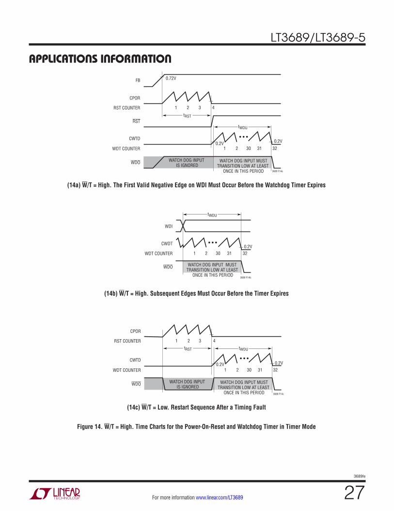
Requirements for the watch dog input in timer mode (W/T = High) are best understood by looking at Figure 14. In timer mode, the WDI pin detects rising and falling edges. These edges are ignored until the power-on-reset timer expires, and the CWDT pin has risen above 0.2V for the first time, as shown in Figure 14a. After that time, there must be an edge on the WDI pin before the watchdog timer expires, which will happen within tWDU (a minimum of 17ms while using 1000pF for CWDT). After this first edge, subsequent edges must follow the timing sequence outlined in Figure 14b. Each subsequent edge must occur before tWDU.
APPLICATIONS INFORMATION
LT3689/LT3689-5
263689fe
For more information www.linear.com/LT3689
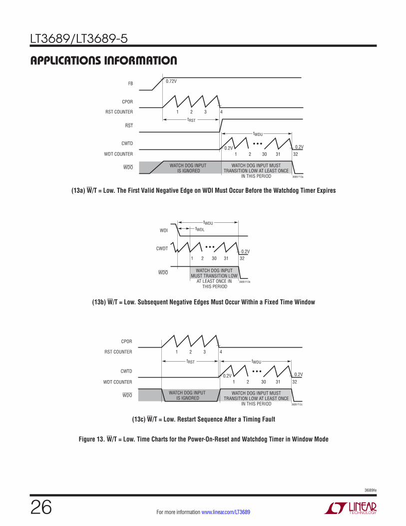
APPLICATIONS INFORMATION
FB 0.72V
0.2V 0.2V
CPOR
CWTD
RST
WDO
RST COUNTER
WDT COUNTER
1 2
tRST
3 4
1 2 30 31 32
3689 F13a
tWDU
WATCH DOG INPUT MUSTTRANSITION LOW AT LEAST ONCE
IN THIS PERIOD
WATCH DOG INPUT IS IGNORED
• • •
(13a) W/T = Low. The First Valid Negative Edge on WDI Must Occur Before the Watchdog Timer Expires
(13b) W/T = Low. Subsequent Negative Edges Must Occur Within a Fixed Time Window
(13c) W/T = Low. Restart Sequence After a Timing Fault
Figure 13. W/T = Low. Time Charts for the Power-On-Reset and Watchdog Timer in Window Mode
0.2V
WDI
CWDT
WDO
tWDUtWDL
32
3689 F13b
313021
WATCH DOG INPUT MUST TRANSITION LOW
AT LEAST ONCE IN THIS PERIOD
• • •
0.2V 0.2V
CPOR
CWTD
WDO
RST COUNTER
WDT COUNTER
1 2 3 4
1 2 30 31 32
3689 F13c
tRST tWDU
WATCH DOG INPUT MUSTTRANSITION LOW AT LEAST ONCE
IN THIS PERIOD
WATCH DOG INPUT IS IGNORED
• • •
LT3689/LT3689-5
273689fe
For more information www.linear.com/LT3689
APPLICATIONS INFORMATION
(14a) W/T = High. The First Valid Negative Edge on WDI Must Occur Before the Watchdog Timer Expires
(14b) W/T = High. Subsequent Edges Must Occur Before the Timer Expires
(14c) W/T = Low. Restart Sequence After a Timing Fault
Figure 14. W/T = High. Time Charts for the Power-On-Reset and Watchdog Timer in Timer Mode
FB 0.72V
CPOR
CWTD
RST
WDO
RST COUNTER
WDT COUNTER
1
1 2 30 31 32
3689 F14a
0.2V0.2V
2
tRST
3 4
tWDU
WATCH DOG INPUT MUSTTRANSITION LOW AT LEAST
ONCE IN THIS PERIOD
WATCH DOG INPUT IS IGNORED
• • •
WDI
CWDT0.2V
3689 F14b
1 2 30 31 32
WDO
WDT COUNTER
tWDU
• • •
WATCH DOG INPUT MUST TRANSITION LOW AT LEAST
ONCE IN THIS PERIOD
CPOR
CWTD
WDO
RST COUNTER
WDT COUNTER
1
1 2 30 31 320.2V 0.2V
3689 F14c
2
tRST
3 4
tWDU
WATCH DOG INPUT MUSTTRANSITION LOW AT LEAST
ONCE IN THIS PERIOD
WATCH DOG INPUT IS IGNORED
• • •
LT3689/LT3689-5
283689fe
For more information www.linear.com/LT3689
If there is a timing fault, the WDO pin will flag, low, and will initiate a restart sequence using the power-on-reset timer, as shown in Figure 14c. The RST pin will remain high, however. WDI edges are ignored until the power-on-reset timer expires, and the CWDT pin has risen above 0.2V for the first time. After that time, there must be an edge on the WDI pin before the watchdog timer expires, which will happen within tWDU. After this first falling edge, subsequent edges must follow the timing sequence out-lined in Figure 14b.
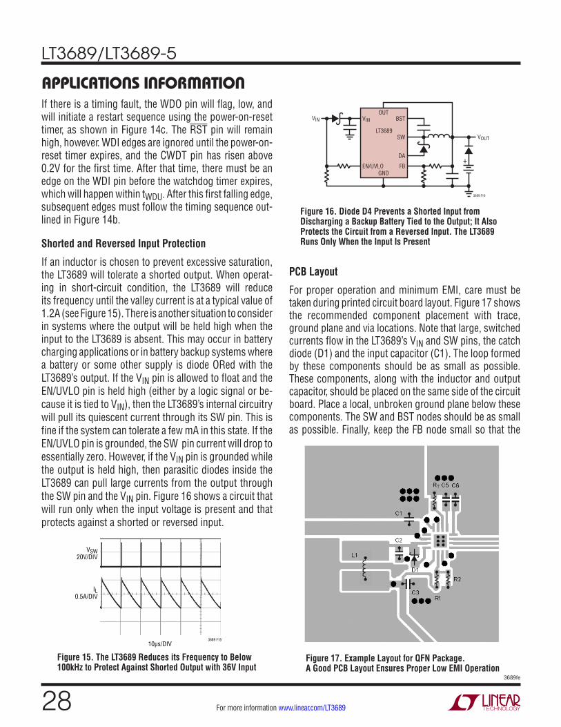
Shorted and Reversed Input Protection
If an inductor is chosen to prevent excessive saturation, the LT3689 will tolerate a shorted output. When operat-ing in short-circuit condition, the LT3689 will reduce its frequency until the valley current is at a typical value of 1.2A (see Figure 15). There is another situation to consider in systems where the output will be held high when the input to the LT3689 is absent. This may occur in battery charging applications or in battery backup systems where a battery or some other supply is diode ORed with the LT3689’s output. If the VIN pin is allowed to float and the EN/UVLO pin is held high (either by a logic signal or be-cause it is tied to VIN), then the LT3689’s internal circuitry will pull its quiescent current through its SW pin. This is fine if the system can tolerate a few mA in this state. If the EN/UVLO pin is grounded, the SW pin current will drop to essentially zero. However, if the VIN pin is grounded while the output is held high, then parasitic diodes inside the LT3689 can pull large currents from the output through the SW pin and the VIN pin. Figure 16 shows a circuit that will run only when the input voltage is present and that protects against a shorted or reversed input.
PCB Layout
For proper operation and minimum EMI, care must be taken during printed circuit board layout. Figure 17 shows the recommended component placement with trace, ground plane and via locations. Note that large, switched currents flow in the LT3689’s VIN and SW pins, the catch diode (D1) and the input capacitor (C1). The loop formed by these components should be as small as possible. These components, along with the inductor and output capacitor, should be placed on the same side of the circuit board. Place a local, unbroken ground plane below these components. The SW and BST nodes should be as small as possible. Finally, keep the FB node small so that the
APPLICATIONS INFORMATION
Figure 17. Example Layout for QFN Package. A Good PCB Layout Ensures Proper Low EMI Operation
Figure 15. The LT3689 Reduces its Frequency to Below 100kHz to Protect Against Shorted Output with 36V Input
Figure 16. Diode D4 Prevents a Shorted Input from Discharging a Backup Battery Tied to the Output; It Also Protects the Circuit from a Reversed Input. The LT3689 Runs Only When the Input Is Present
VIN
3689 F16
EN/UVLO
BST
SWLT3689
OUT
GND
DA
FB
VIN
VOUT
+
10µs/DIV
VSW20V/DIV
IL0.5A/DIV
3689 F15
LT3689/LT3689-5
293689fe
For more information www.linear.com/LT3689
ground traces will shield them from the SW and BOOST nodes. The Exposed Pad on the bottom of the package must be soldered to ground so that the pad acts as a heat sink. To keep thermal resistance low, extend the ground plane as much as possible, and add thermal vias under and near the LT3689 to additional ground planes within the circuit board and on the bottom side.
High Temperature Considerations
The PCB must provide heat sinking to keep the LT3689 cool. The Exposed Pad on the bottom of the package must be soldered to a ground plane. This ground should be tied to large copper layers below with thermal vias; these layers will spread the heat dissipated by the LT3689. Placing additional vias can reduce thermal resistance further. Because of the large output current capability of the LT3689, it is possible to dissipate enough heat to raise the junction temperature beyond the absolute maximum of 125°C (150°C for H-grade). When operating at high ambient temperatures, the maximum load current should
be derated as the ambient temperature approaches 125°C (150°C for H-grade). A board measuring 5cm × 7.5cm with a top layer layout similar to Figure 15 was evaluated in still air at 3.3VOUT, 700kHz switching frequency. At 700mA load, the temperature reached approximately 12°C above ambient for input voltages equal to 12V and 24V. Power dissipation within the LT3689 can be estimated by calculat-ing the total power loss from an efficiency measurement and subtracting the catch diode loss. The die temperature is calculated by multiplying the LT3689 power dissipation by the thermal resistance from junction-to-ambient.
Other Linear Technology Publications
Application Notes 19, 35 and 44 contain more detailed descriptions and design information for buck regulators and other switching regulators. The LT1376 data sheet has a more extensive discussion of output ripple, loop compensation and stability testing. Design Note 318 shows how to generate a bipolar output supply using a buck regulator.
APPLICATIONS INFORMATION
TYPICAL APPLICATIONS
SW
DAFBRT
SYNC
fSW = 1MHz
WDI
RST
WDO
VIN EN/UVLO
VIN6.3V TO 36VTRANSIENT
TO 60V
5V700mA
R2102k
L112µH
C20.1µF
D1
C310µF
R1536k
GND
RT12.7k
LT3689
3689 TA02
BSTOUT
CPOR
CWDT
C11µF
I/O
I/O
RESET
µP
W/TWINDOW TIMEOUT
WDEWATCHDOG_DEFEAT
C610nFtWDU = 182ms
L1: CDR125NP-12MCD1: MBRM140C1, C2, C3: X7R or X5R
C45.6pF
C568nFtRST = 157ms
5V Step-Down Converter

LT3689/LT3689-5
303689fe
For more information www.linear.com/LT3689
TYPICAL APPLICATIONS
SW
DAFBRT
SYNC
fSW = 700kHz
WDI
RST
WDO
VIN EN/UVLO
VIN4.5V TO 36VTRANSIENT
TO 60V
3.3V700mA
R2100k
L112µH
C20.1µF
D1
C322µF
R1316k
GND
RT20.5k
LT3689
3689 TA03
BSTOUT
CPOR
CWDT
C12.2µF
I/O
I/O
RESET
µP
W/TWINDOW TIMEOUT
WDEWATCHDOG_DEFEAT
C610nFtWDU = 182ms
L1: CDR125NP-12MCD1: MBRM140C1, C2, C3: X7R or X5R
C410pF
C568nFtRST = 157ms
3.3V Step-Down Converter
SW
DAFBRT
SYNC
fSW = 2MHz
WDI
RST
WDO
VIN EN/UVLO
VIN6.3V TO 18VTRANSIENT
TO 60V
5V700mA
L110µH
C20.1µF
D1
C34.7µF
GNDRT4.02k
LT3689-5
3689 TA04
BSTOUT
CPOR
CWDT
C11µF
I/O
I/O
RESET
µP
W/TWINDOW TIMEOUT
WDEWATCHDOG_DEFEAT
C610nFtWDU = 182ms
C1, C2, C3: X7R OR X5RD1: MBRM140
C42.7pF
C568nFtRST = 157ms
5V, 2MHz Step-Down Converter
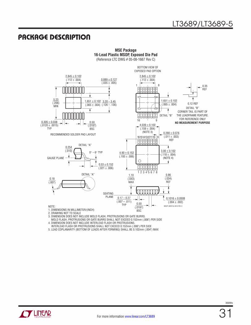
LT3689/LT3689-5
313689fe
For more information www.linear.com/LT3689
PACKAGE DESCRIPTION
MSOP (MSE16) 0910 REV C
0.53 ± 0.152(.021 ± .006)
SEATINGPLANE
0.18(.007)
1.10(.043)MAX
0.17 – 0.27(.007 – .011)
TYP
0.86(.034)REF
0.50(.0197)
BSC
16
16151413121110
1 2 3 4 5 6 7 8
9
9
1 8
NOTE:1. DIMENSIONS IN MILLIMETER/(INCH)2. DRAWING NOT TO SCALE3. DIMENSION DOES NOT INCLUDE MOLD FLASH, PROTRUSIONS OR GATE BURRS. MOLD FLASH, PROTRUSIONS OR GATE BURRS SHALL NOT EXCEED 0.152mm (.006") PER SIDE4. DIMENSION DOES NOT INCLUDE INTERLEAD FLASH OR PROTRUSIONS. INTERLEAD FLASH OR PROTRUSIONS SHALL NOT EXCEED 0.152mm (.006") PER SIDE5. LEAD COPLANARITY (BOTTOM OF LEADS AFTER FORMING) SHALL BE 0.102mm (.004") MAX
0.254(.010) 0° – 6° TYP
DETAIL “A”
DETAIL “A”
GAUGE PLANE
5.23(.206)MIN
3.20 – 3.45(.126 – .136)
0.889 ± 0.127(.035 ± .005)
RECOMMENDED SOLDER PAD LAYOUT
0.305 ± 0.038(.0120 ± .0015)
TYP
0.50(.0197)
BSC
BOTTOM VIEW OFEXPOSED PAD OPTION
2.845 ± 0.102(.112 ± .004)
2.845 ± 0.102(.112 ± .004)
4.039 ± 0.102(.159 ± .004)
(NOTE 3)
1.651 ± 0.102(.065 ± .004)
1.651 ± 0.102(.065 ± .004)
0.1016 ± 0.0508(.004 ± .002)
3.00 ± 0.102(.118 ± .004)
(NOTE 4)
0.280 ± 0.076(.011 ± .003)
REF
4.90 ± 0.152(.193 ± .006)
DETAIL “B”
DETAIL “B”CORNER TAIL IS PART OF
THE LEADFRAME FEATURE.FOR REFERENCE ONLY
NO MEASUREMENT PURPOSE
0.12 REF
0.35REF
MSE Package16-Lead Plastic MSOP, Exposed Die Pad
(Reference LTC DWG # 05-08-1667 Rev C)
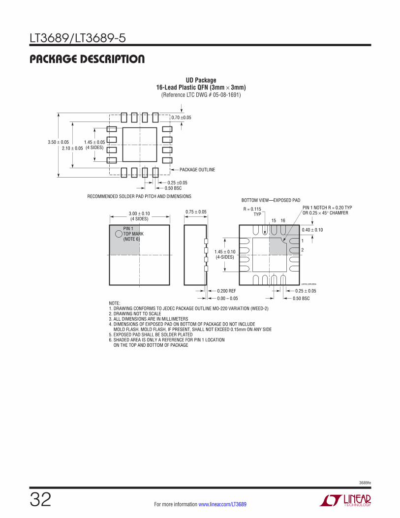
LT3689/LT3689-5
323689fe
For more information www.linear.com/LT3689
PACKAGE DESCRIPTION
3.00 ± 0.10(4 SIDES)
RECOMMENDED SOLDER PAD PITCH AND DIMENSIONS
1.45 ± 0.05(4 SIDES)
NOTE:1. DRAWING CONFORMS TO JEDEC PACKAGE OUTLINE MO-220 VARIATION (WEED-2)2. DRAWING NOT TO SCALE3. ALL DIMENSIONS ARE IN MILLIMETERS4. DIMENSIONS OF EXPOSED PAD ON BOTTOM OF PACKAGE DO NOT INCLUDE MOLD FLASH. MOLD FLASH, IF PRESENT, SHALL NOT EXCEED 0.15mm ON ANY SIDE5. EXPOSED PAD SHALL BE SOLDER PLATED6. SHADED AREA IS ONLY A REFERENCE FOR PIN 1 LOCATION ON THE TOP AND BOTTOM OF PACKAGE
PIN 1TOP MARK(NOTE 6)
0.40 ± 0.10
BOTTOM VIEW—EXPOSED PAD
1.45 ± 0.10(4-SIDES)
0.75 ± 0.05 R = 0.115TYP
0.25 ± 0.05
1
PIN 1 NOTCH R = 0.20 TYPOR 0.25 × 45° CHAMFER
15 16
2
0.50 BSC
0.200 REF
2.10 ± 0.053.50 ± 0.05
0.70 ±0.05
0.00 – 0.05
(UD16) QFN 0904
0.25 ±0.050.50 BSC
PACKAGE OUTLINE
UD Package16-Lead Plastic QFN (3mm × 3mm)
(Reference LTC DWG # 05-08-1691)
LT3689/LT3689-5
333689fe
For more information www.linear.com/LT3689
Information furnished by Linear Technology Corporation is believed to be accurate and reliable. However, no responsibility is assumed for its use. Linear Technology Corporation makes no representa-tion that the interconnection of its circuits as described herein will not infringe on existing patent rights.
REVISION HISTORYREV DATE DESCRIPTION PAGE NUMBER
A 4/10 Added LT3689-5 Fixed Output Voltage Option 1–32
B 9/10 Revised conditions for tSW(OFF) and VOL in Electrical Characteristics section. 3
C 10/10 Removed connection from OUT to GND in 5V, 2MHz Step-Down Converter drawing in Typical Applications section. 28
D 2/11 Replaced Figure 12 in the Applications Information section. 24
E 3/13 Clarified Switching Frequency limits, Foldback Resistor valuesClarified Watchdog Timing graphs
325-28
LT3689/LT3689-5
343689fe
For more information www.linear.com/LT3689 LINEAR TECHNOLOGY CORPORATION 2010
LT 0613 REV E • PRINTED IN USALinear Technology Corporation1630 McCarthy Blvd., Milpitas, CA 95035-7417(408) 432-1900 ● FAX: (408) 434-0507 ● www.linear.com/LT3689
RELATED PARTS
TYPICAL APPLICATION
PART NUMBER DESCRIPTION COMMENTS
LT1766 60V, 1.2A (IOUT), 200kHz, High Efficiency Step-Down DC/DC Converter
VIN: 5.5V to 60V, VOUT(MIN) = 1.20V, IQ = 2.5mA, ISD = 25µA, TSSOP-16 and TSSOP-16E Packages
LT1936 36V, 1.4A (IOUT), 500kHz High Efficiency Step-Down DC/DC Converter
VIN: 3.6V to 36V, VOUT(MIN) = 1.2V, IQ = 1.9mA, ISD <1µA, MS8E Package
LT1976/LT1977 60V, 1.2A (IOUT), 200kHz/500kHz, High Efficiency Step-Down DC/DC Converter with Burst Mode Operation
VIN: 3.3V to 60V, VOUT(MIN) = 1.20V, IQ = 100µA, ISD <1µA, TSSOP-16E Package
LT3434/LT3435 60V, 2.4A (IOUT), 200kHz/500kHz, High Efficiency Step-Down DC/DC Converter with Burst Mode Operation
VIN: 3.3V to 60V, VOUT(MIN) = 1.20V, IQ = 100mA, ISD <1µA, TSSOP-16E Package
LT3437 60V, 400mA (IOUT), Micropower Step-Down DC/DC Converter with Burst Mode Operation
VIN: 3.3V to 60V, VOUT(MIN) = 1.25V, IQ = 100µA, ISD <1µA, 3mm × 3mm DFN-10 and TSSOP-16E Packages
LT3480 36V with Transient Protection to 60V, 2A (IOUT), 2.4MHz, High Efficiency Step-Down DC/DC Converter with Burst Mode Operation
VIN: 3.6V to 38V, VOUT(MIN) = 0.78V, IQ = 70µA, ISD <1µA, 3mm × 3mm DFN-10 and MSOP-10E Packages
LT3481 34V with Transient Protection to 36V, 2A (IOUT), 2.8MHz, High Efficiency Step-Down DC/DC Converter with Burst Mode Operation
VIN: 3.6V to 34V, VOUT(MIN) = 1.26V, IQ = 50mA, ISD <1µA, 3mm × 3mm DFN-10 and MSOP-10E Packages
LT3493 36V, 1.4A (IOUT), 750kHz High Efficiency Step-Down DC/DC Converter
VIN: 3.6V to 36V, VOUT(MIN) = 0.8V, IQ = 1.9mA, ISD <1µA, 2mm × 3mm DFN-6 Package
LT3500 36V, 40VMAX, 2A, 2.5MHz High Efficiency Step-Down DC/DC Converter and LDO Controller
VIN: 3.6V to 36V, VOUT(MIN) = 0.8V, IQ = 2.5mA, ISD <10µA, 3mm × 3mm DFN-10 Package
LT3505 36V with Transient Protection to 40V, 1.4A (IOUT), 3MHz, High Efficiency Step-Down DC/DC Converter
VIN: 3.6V to 34V, VOUT(MIN) = 0.78V, IQ = 2mA, ISD = 2µA, 3mm × 3mm DFN-8 and MSOP-8E Packages
LT3507 36V 2.5MHz, Triple (2.4A + 1.5A + 1.5A (IOUT)) with LDO Controller High Efficiency Step-Down DC/DC Converter
VIN: 3.6V to 36V, VOUT(MIN) = 0.8V, IQ = 2.5mA, ISD = 10µA, TSSOP-16 and TSSOP-16E Packages
LT3508 36V with Transient Protection to 40V, Dual 1.4A (IOUT), 3MHz, High Efficiency Step-Down DC/DC Converter
VIN: 3.7V to 37V, VOUT(MIN) = 0.8V, IQ = 4.6mA, ISD = 1µA, 4mm × 4mm QFN-24 and TSSOP-16E Packages
LT3682 36V, 60VMAX, 1A, 2.2MHz High Efficiency Micropower Step-Down DC/DC Converter
VIN: 3.6V to 36V, VOUT(MIN) = 0.8V, IQ = 75mA, ISD <1µA, 3mm × 3mm DFN-12 Package
LT3684 34V with Transient Protection to 36V, 2A (IOUT), 2.8MHz, High Efficiency Step-Down DC/DC Converter
VIN: 3.6V to 34V, VOUT(MIN) = 1.26V, IQ = 850µA, ISD <1µA, 3mm × 3mm DFN-10 and MSOP-10E Packages
LT3685 36V with Transient Protection to 60V, 2A (IOUT), 2.4MHz, High Efficiency Step-Down DC/DC Converter
VIN: 3.6V to 38V, VOUT(MIN) = 0.78V, IQ = 70µA, ISD <1µA, 3mm × 3mm DFN-10 and MSOP-10E Packages
SW
DAFBRT
SYNC
fSW = 900kHz
WDI
RST
WDO
VIN EN/UVLO
VIN3.6V TO 16V
TRANSIENT TO 27V
1.8V700mA
R2102k
L14.7µH
C20.1µF
D1
C347µF
R1127k
GND
RT14.7k
LT3689
3689 TA05
BSTOUT
CPOR
CWDT
C11µF
I/O
RESET
µP
W/TWINDOW TIMEOUT
WDEWATCHDOG_DEFEAT
C610nFtWDU = 182msL1: WE-PD2: 7447745047
D1: MBRM140C1, C2, C3: X7R OR X5R
C415pF
C568nFtRST = 157ms
1.8V Step-Down Converter with System Reset Generated by Watchdog Timing or Output Voltage Failure