Embed Size (px)
Citation preview

Confidential, subject to all applicable non-disclosure agreements www.SanDisk.com
Industrial iNAND® 7250-I
e.MMC 5.1 with HS400 Interface
DOC-56-34-01460• Rev 1.1 • May 2017
Data Sheet - Confidential

Confidential SanDisk® iNAND 7250 e.MMC 5.1+ HS400 I/F data sheet
© 2017 SanDisk – a Western Digital brand - 2 - DOC-56-34-01460
REVISION HISTORY
Doc. No Revision Date Description
DOC-56-34-01460 0.1 October-2016 Preliminary version
DOC-56-34-01460 0.2 January-2017 Updated tables 2, 5 and 6
DOC-56-34-01460 1.0 March-2017 Released version
DOC-56-34-01460 1.1 May-2017 Updated SKU names
SanDisk® general policy does not recommend the use of its products in life support applications where in a failure or malfunction of the product may directly threaten life or injury. Per SanDisk Terms and Conditions of Sale, the user of SanDisk products in life support applications assumes all risk of such use and indemnifies SanDisk against all damages. See “Disclaimer of Liability.” This document is for information use only and is subject to change without prior notice. SanDisk assumes no responsibility for any errors that may appear in this document, nor for incidental or consequential damages resulting from the furnishing, performance or use of this material. No part of this document may be reproduced, transmitted, transcribed, stored in a retrievable manner or translated into any language or computer language, in any form or by any means, electronic, mechanical, magnetic, optical, chemical, manual or otherwise, without the prior written consent of an officer of SanDisk . SanDisk provides this information, and any related samples, products, and documentation (collectively the “Materials”) solely for the selection and use of SanDisk products. To the maximum extent permitted by applicable law: (1) Materials are made available “AS IS” and with all faults, SanDisk hereby DISCLAIMS ALL WARRANTIES AND CONDITIONS, EXPRESS, IMPLIED, STATUTORY, OR OTHERWISE, INCLUDING BUT NOT LIMITED TO WARRANTIES OF MERCHANTABILITY, NON-INFRINGEMENT, OR FITNESS FOR ANY PARTICULAR PURPOSE; and (2) SanDisk shall not be liable (whether in contract or tort, including negligence, or under any other theory of liability) for any loss or damage of any kind or nature related to, arising under, or in connection with, the Materials (including your use of the Materials), including for any direct, indirect, special, incidental, or consequential loss or damage (including loss of data, profits, goodwill, or any type of loss or damage suffered as a result of any action brought by a third party) even if such damage or loss was reasonably foreseeable or SanDisk had been advised of the possibility of the same. You are responsible for obtaining any rights required in connection with your use of the Materials. The Materials are subject to change without further notice. SanDisk assumes no obligation to correct errors or to notify you of updates to the Materials or to product specifications. You may not reverse engineer, reproduce, modify, distribute, or publicly display the Materials without prior written consent of SanDisk. SanDisk products are not designed or intended to be fail-safe or for use in any application requiring fail-safe performance. You assume sole risk and liability for use of SanDisk products in critical applications. All parts of the SanDisk documentation are protected by copyright law and all rights are reserved. SanDisk and the SanDisk logo are registered trademarks of SanDisk. Product names mentioned herein are for identification purposes only and may be trademarks and/or registered trademarks of their respective companies. Western Digital Technologies, Inc. is the seller of record and licensee in the Americas of SanDisk® products. ©2017 Western Digital Corporation or its affiliates. All rights reserved. SanDisk is a trademark of Western Digital Corporation or its affiliates, registered in the United States and other countries. All other trademarks are the property of their respective holder(s).

Confidential
SanDisk® iNAND 7250 e.MMC 5.1+ HS400 I/F data sheet
© 2017 SanDisk – a Western Digital brand - 3 - DOC-56-34-01460
TABLE OF CONTENTS
1. Introduction ......................................................................................................................... 5
1.1. General Description ...................................................................................................... 5
1.2. Plug-and-Play Integration ................................................................................................. 6
1.3. Feature Overview ......................................................................................................... 7
1.4. MMC bus and Power Lines ........................................................................................... 8
1.4.1. Bus operating conditions ................................................................................................. 8
2. e.MMC Selected Features Overview ................................................................................ 10
2.1. HS400 Interface .......................................................................................................... 11
2.2. Enhanced User Data Area (EUDA) ............................................................................. 11
2.3. Extended Partitions Attribute (eGPP) .......................................................................... 11
2.4. Field Firmware Upgrade (FFU) ................................................................................... 11
2.5. Cache ......................................................................................................................... 12
2.6. Discard ....................................................................................................................... 12
2.7. Power off Notifications ................................................................................................ 12
2.8. Packed Commands .................................................................................................... 12
2.9. Boot Partition .............................................................................................................. 12
2.10. RPMB Partition ........................................................................................................... 12
2.11. Automatic Sleep Mode ................................................................................................ 12
2.12. Sleep (CMD5) ............................................................................................................. 13
2.13. Enhanced Reliable Write ............................................................................................ 13
2.14. Sanitize ...................................................................................................................... 13
2.15. Secure Erase .............................................................................................................. 13
2.16. Secure Trim ................................................................................................................ 14
2.17. Partition Management................................................................................................. 14
2.18. Device Health ............................................................................................................. 14
2.19. EOL Status ................................................................................................................. 14
2.20. Enhanced Write Protection ......................................................................................... 14
2.21. High Priority Interrupt (HPI)......................................................................................... 15
2.22. H/W Reset .................................................................................................................. 15
2.23. Host-Device Synchronization Flow (Enhanced STROBE) ........................................... 15
2.24. Command-Queue ....................................................................................................... 15
3. Product Specifications ..................................................................................................... 16
3.1. Typical Power Requirements ...................................................................................... 16

Confidential
SanDisk® iNAND 7250 e.MMC 5.1+ HS400 I/F data sheet
© 2017 SanDisk – a Western Digital brand - 4 - DOC-56-34-01460
3.2. Operating Conditions .................................................................................................. 17
3.2.1. Operating and Storage Temperature Specifications ..................................................... 17
3.2.2. Moisture Sensitivity ........................................................................................................ 17
3.3. Reliability .................................................................................................................... 18
3.5. Typical System Performance ...................................................................................... 19
4. Physical Specifications .................................................................................................... 20
5. Interface Description ......................................................................................................... 22
5.1. MMC I/F Ball Array ..................................................................................................... 22
5.2. Pins and Signal Description ........................................................................................ 23
5.3. Registers value ........................................................................................................... 24
5.3.1. OCR Register................................................................................................................. 24
5.3.2. CID Register .................................................................................................................. 24
5.3.3. DSR Register ................................................................................................................. 24
5.3.4. CSD Register ................................................................................................................. 25
5.3.5. EXT_CSD Register ........................................................................................................ 26
5.4. User Density ............................................................................................................... 31
6. HW Application Guidelines ............................................................................................... 32
6.1. Design Guidelines ...................................................................................................... 32
6.2. Capacitor Selection & Layout Guidelines .................................................................... 33
6.3. Reference Schematics ................................................................................................ 35
7. Propriety iNAND 7250 feature overview .......................................................................... 36
7.1. Smart Partitioning ....................................................................................................... 36
7.2. Manual Refresh .......................................................................................................... 36
7.3. Boot & RPMB resize ................................................................................................... 36
7.4. One Time Programmable Register for Custom ID ....................................................... 37
7.5. Device Report & Advanced Health Status................................................................... 37
7.5.1. Device Report fields ....................................................................................................... 37
7.5.2. Advanced Health Status Fields...................................................................................... 38
7.6. Power-Loss indications ............................................................................................... 39
7.6.1. Unstable Power-Supply indications ............................................................................... 39
8. Marking .............................................................................................................................. 41
9. Ordering Information ........................................................................................................ 42
How to Contact Us .................................................................................................................. 43

Confidential DOC-56-34-01460
SanDisk iNAND 7250 e.MMC 5.1 HS400 I/F data sheet
© 2017 SanDisk – a Western Digital brand - 5 - DOC-56-34-01460
1. INTRODUCTION
1.1. General Description
Overview The SanDisk® Industrial iNAND 7250 is an Embedded Flash Drive (EFD) designed for connected devices in Industrial, Industrial IoT, and other IoT applications. This includes applications such as security cameras, commercial drones, networking equipment, IoT gateways, system on modules (SOM), and others. The Industrial iNAND 7250 enables manufacturers to bring the benefits of flash rapid boot-up, high reliability, robustness, consistent performance as well as many proprietary features to these new applications. The Industrial iNAND 7250 utilizes an LDPC ECC engine and MLC memory to provide a robust, high performance, high quality and high endurance product. The LDPC engine significantly improves error correction capabilities enabling longer device lifetime and an increased ability to handle operations at high temperature. The MLC memory is optimized versus standard MLC memory to offer better endurance over the life of the memory, providing more design margin, and also leading to a lower uncorrectable bit-error rate (UBER) at any given point over the life of the device.
The SanDisk Industrial iNAND 7250 was designed with a specific focus on the Industrial market. All SanDisk Industrial grade products go through extensive testing, and are part of a long-term, stable roadmap, reducing the complexity and number of qualification cycles that a manufacturer may need to perform. The Industrial iNAND 7250 is qualified to temperature ranges from -40oC up to 85oC ambient.
The Industrial iNAND 7250 is available from 8GB to 64GB of capacity and supports the e.MMC 5.1 interface. Highlighted features include extended operating temperature support, advanced health status, automatic and manual data refresh, RPMB and Boot partition resize, flexible EUDA and fast boot mode. Data reliability and product life is improved significantly by the internal refresh feature combined with MLC memory and LDPC ECC engine. Industrial iNAND 7250 also provides 3.3V IO support for legacy designs and hence is suitable for upgrading old systems.
Architecture The Industrial iNAND 7250 combines an embedded flash controller with Multi-level Cell NAND flash technology enhanced by SanDisk’s embedded flash management software running as firmware on the flash controller. Industrial iNAND 7250 employs an industry-standard e.MMC 5.1 interface featuring Command-Queue, HS400 interface, FFU, as well as legacy e.MMC 4.51 features such as power off notifications, packed commands, Cache, boot / RPMB partitions, HPI, and HW reset, making it an optimal device for both reliable code and data storage.
Like other SanDisk iNAND products, the Industrial iNAND 7250 offers plug-and-play integration and support for multiple NAND technology transitions.
The Industrial iNAND 7250 architecture and embedded firmware fully emulates a hard disk to the host processor, enabling read/write operations that are identical to a standard, sector-based hard drive. In addition, SanDisk firmware employs patented methods, such as virtual

© 2017 SanDisk – a Western Digital brand - 6 - DOC-56-34-01460
mapping, dynamic and static wear-leveling, and automatic block management to ensure high data reliability and maximizing flash life expectancy.
The Industrial iNAND 7250 also includes an intelligent controller, which manages interface protocols, data storage and retrieval, error correction code (ECC) algorithms, defect handling and diagnostics, power management and clock control.
Combining high performance with features for easy integration and exceptional reliability, the Industrial iNAND 7250 is an EFD designed to exceed the demands of both manufacturers and their customers.
1.2. Plug-and-Play Integration
iNAND’s optimized architecture eliminates the need for complicated software integration and testing processes thereby enabling plug-and-play integration into the host system. The replacement of one iNAND device with another of a newer generation requires virtually no changes to the host. This allows manufacturers to adopt advanced NAND Flash technologies and update product lines with minimal integration or qualification efforts.
The Industrial iNAND 7250 features a MMC interface that allows for easy integration regardless of the host (chipset) type used. All device and interface configuration data (such as maximum frequency and device identification) are stored on the device.
With JEDEC compatible form factors measuring 11.5x13mm (153 balls) for all capacities, the Industrial iNAND 7250 is ideally suited for a wide variety of Industrial subsystems where PCB space may be limited.
Figure 1 shows a block diagram of the SanDisk Industrial iNAND 7250 with MMC Interface.
Figure 1 - SanDisk Industrial iNAND 7250 with MMC Interface Block Diagram
Data In/Out
MMC Bus Interface
Single Chip controller
Control
Flash Memory
SanDisk iNAND

© 2017 SanDisk – a Western Digital brand - 7 - DOC-56-34-01460
1.3. Feature Overview
SanDisk Industrial iNAND 7250, with MMC interface, includes the following features:
Memory controller and NAND flash
Mechanical design that complies with JEDEC Specifications with specific optimizations for industrial applications
Offered in three TFBGA packages of e.MMC 5.1
o 11.5mm x 13mm x 0.8mm (8GB-16GB)
o 11.5mm x 13mm x 1.0mm (32GB)
o 11.5mm x 13mm x 1.2mm (64GB)
Operating temperature range: –25°C to +85°C and –40°C to +85°C ambient
Dual power system
Core voltage (VCC) 2.7-3.6 V
I/O (VCCQ) voltage, either: 1.7-1.95V or 2.7-3.6V
8GB - 64GB of data storage
Supports three data bus widths: 1bit (default), 4bit, 8bit
Complies with e.MMC Specification Ver. 5.1 HS400
Variable clock frequencies of 0-20 MHz, 0-26 MHz (default), 0-52 MHz (high-speed), 0-200 MHz SDR (HS200), 0-200 MHz DDR (HS400)
Up to 400 MB/sec bus transfer rate, using 8 parallel data lines at 200 MHz, HS400 Mode
High data integrity with MLC memory, advanced LDPC ECC engine, automatic and manual refresh
Advanced health status, fast boot, flexible EUDA, smart partitioning
Up to 3K P/E cycles on MLC and 30K P/E cycles on SLC with 1 year data retention @ 55°C and at least 10 year data retention @ 55°C for fresh devices
© 2017 SanDisk – a Western Digital brand - 8 - DOC-56-34-01460
1.4. MMC bus and Power Lines
SanDisk iNAND 7250 supports the MMC interface protocol. For more details regarding these buses refer to JEDEC standard No. JESD84-B51.
The iNAND bus has the following communication and power lines:
CMD: Command is a bidirectional signal. The host and iNAND operate in two modes, open drain and push-pull.
DAT0-7: Data lines are bidirectional signals. Host and iNAND operate in push-pull mode.
CLK: Clock input.
RST_n: Hardware Reset Input.
VCCQ: Power supply line for host interface.
VCC: Power supply line for internal flash memory.
VDDi: iNAND’s internal power node, not the power supply. Connect 0.1uF capacitor from VDDi to ground.
VSS, VSSQ: Ground lines.
RCLK: Data strobe.
VSF: Vendor specific functions used for debugging purposes.
1.4.1. Bus operating conditions
Table 1 - Bus operating conditions
Parameter Min Max Unit
Peak voltage on all lines -0.5 VCCQ+0.5 V
Input Leakage Current (before initializing
and/or connecting the internal pull-up
resistors)
-100 100 µA
Input Leakage Current (after changing the
bus width and disconnecting the internal
pull-up resistors)
-2 2 µA
Output Leakage Current (before initializing
and/or connecting the internal pull-up
resistors)
-100 100 µA
Output Leakage Current (after changing
the bus width and disconnecting the
internal pull-up resistors)
-2 2 µA

© 2017 SanDisk – a Western Digital brand - 9 - DOC-56-34-01460
Table 2 – Power supply voltage
Parameter Symbol Min Max Unit
Supply Voltage
VCCQ (Low) 1.7 1.95 V
VCCQ (High) 2.7 3.6 V
VCC 2.7 3.6 V
VSS-VSSQ -0.3 0.3 V

© 2017 SanDisk – a Western Digital brand - 10 - DOC-56-34-01460
2. E.MMC SELECTED FEATURES OVERVIEW Industrial iNAND 7250 supported feature list:
Table 3 – Proprietary Features list e.MMC Device Features Benefit Support
N/A INTERFACE Speed HS400
N/A BUS SPEED Max theoretical Speed Up to 400MB/s
4.41 SECURE ERASE/TRIM “True Wipe” Yes
4.41 BOOT AND MASS STORAGE One storage device (reduced BOM) Yes
4.41 PARTITIONING & PROTECTION Flexibility Yes
4.41 BACKGROUND OPERATIONS Better User Experience (low latency) Yes
4.41 POWER OFF NOTIFICATION Faster Boot; Responsiveness Yes
4.41 HARDWARE RESET Robust System Design Yes
4.41 HPI Control Long Reads/Writes Yes
4.41 RPMB Secure Folders Yes
4.5 EXTENDED PARTITION ATTRIBUTE Flexibility Yes
4.5 LARGE SECTOR SIZE Potential performance No
4.5 SANITIZE (4.51) “True Wipe” Yes
4.5 PACKED COMMANDS Reduce Host Overhead Yes
4.5 DISCARD Improved Performance on Full Media Yes
4.5 DATA TAG Performance and/or Reliability Yes (API only)
4.5 CONTEXT MANAGEMENT Performance and/or Reliability Yes (API only)
4.5 CACHE Better Sequential & Random Writes Yes
5.0 FIELD FIRMWARE UPGRADE (FFU) Enables feature enhancements in the field Yes
5.0 PRODUCTION STATE AWARENESS Different operation during production Yes
5.0 DEVICE HEALTH Vital NAND info Yes
5.1 ENHANCE STROBE Sync between Device and Host in HS400 Yes
5.1 COMMAND QUEUE Responsiveness Yes
5.1 RPMB THROUGHPUT Faster RPMB write throughput Yes
5.1 CACHE FLUSH AND BARRIER Ordered Cache flushing Yes
5.1 BKOPS CONTROLLER Host control on BKOPs Yes
5.1 SECURE WP Secure Write Protect Yes
5.1 EUDA Enhanced User Data Area Yes
Proprietary VSF Enable on-board debugging Yes
Proprietary PNM Special product name Yes
Proprietary DEVICE REPORT Device Firmware status Yes
Proprietary BOOT PARTITION RESIZE User configurable boot partition Yes
Proprietary RPMB RESIZE User configurable RPMB partition Yes
Proprietary MANUAL READ SCRUB Host initiated refresh Yes
Proprietary QUICK MOUNT Fast boot to all user partitions Yes
Proprietary AUTOMATIC READ REFRESH Automatic scans to detect blocks for refresh Yes
Proprietary ADVANCED HEALTH STATUS Includes PE cycles in % per partition, temperature Yes

© 2017 SanDisk – a Western Digital brand - 11 - DOC-56-34-01460
2.1. HS400 Interface
Industrial iNAND 7250 supports HS400 signaling to achieve a bus speed of 400 MB/s via a 200MHz dual data rate clock frequency. HS400 mode supports 4 or 8 bit bus width and the 1.7 – 1.95 VCCQ option. Due to the speed, the host may need to have an adjustable sampling point to reliably receive the incoming data. For additional information please refer to JESD84-B51 standard.
2.2. Enhanced User Data Area (EUDA)
For write intensive applications, there is a need for an area of higher endurance or performance. To address this, Industrial iNAND 7250 allows for the definition of an enhanced user data area as specified in the JESD84-B51 standard. This area is a true SLC partition. The EUDA is a designated area of the general User Data Area. The configuration is one-time programmable.
This is NOT recommended for data that has long retention needs. For OS type data, see section: 2.3 Extended Partitions Attribute for further information.
For additional information please refer to the SanDisk application note on this subject.
2.3. Extended Partitions Attribute (eGPP)
When a device is used as a boot device, the boot code, the operating system code, and any highly secure information is generally rarely written, but needs to be reliably retained for the lifetime of the device. For this purpose, Industrial iNAND 7250 utilizes the System Code Extended Partitions Attribute as specified in the JESD84-B51 standard. This area is a true SLC partition.
This is NOT recommended for write intensive application usage. For high endurance needs, see section: 2.2 Enhanced User Data Area for further information.
For additional information please refer to the SanDisk application note on this subject.
2.4. Field Firmware Upgrade (FFU)
Field Firmware Updates (FFU) enables features enhancement in the field. Using this mechanism,
the host downloads a new version of the firmware to the e.MMC device and instructs the e.MMC device to install the new downloaded firmware into the device. The entire FFU process occurs in the background without affecting the user/OS data. During the FFU process, the host can replace firmware files or single/all file systems.
The secure FFU (sFFU) usage model for firmware upgrades is as follows:
1. sFFU files are generated and signed at the SanDisk lab 2. The sFFU files are handed to SanDisk’s customer 3. SanDisk’s customer can push the firmware updates to their end-users in a transparent
way Note 1: The sFFU process and sFFU files are protected against leakage to unauthorized entities.

© 2017 SanDisk – a Western Digital brand - 12 - DOC-56-34-01460
Note 2: During the sFFU process the Host may retrieve the exact status of the process using the smart report feature.
For additional information please refer to JESD84-B51 standard and the SanDisk application note on this subject.
2.5. Cache
The eMMC cache is dedicated volatile memory at the size of 512KB. Caching enables to improve iNAND performance for both sequential and random access. For additional information please refer to JESD84-B51 standard.
2.6. Discard
iNAND supports discard command as defined in e.MMC 5.1 spec. This command allows the host to identify data which is not needed, without requiring the device to remove the data from the Media. It is highly recommended for use to guarantee optimal performance of iNAND and reduce amount of housekeeping operation.
2.7. Power off Notifications
iNAND supports power off notifications as defined in e.MMC 5.1 spec. The usage of power off notifications allows the device to prepare itself to power off, and improve user experience during power-on. Note that the device may be set into sleep mode while power off notification is enabled.
Power off notification long allows the device to shutdown properly and save important data for fast boot time on the next power cycle.
2.8. Packed Commands
To enable optimal system performance, iNAND supports packed commands as defined in e.MMC 5.1 spec. It allows the host to pack Read or Write commands into groups (of single type of operation) and transfer these to the device in a single transfer on the bus. Thus, it allows reducing overall bus overheads.
2.9. Boot Partition
iNAND supports e.MMC 5.1 boot operation mode: Factory configuration supplies two boot partitions each 4MB in size for 8GB-64GB. This can be expanded to up to 31.875 MB by resizing the boot partitions. See section 7.3 Boot & RPMB resize for further information.
2.10. RPMB Partition
iNAND supports e.MMC 5.1 RPMB operation mode: Factory configuration supplies one RPMB partition 4MB in size for 8GB-64GB. This can be expanded to up to 16 MB by resizing the RPMB partition. See section: See section 7.3 Boot & RPMB resize for further information.
2.11. Automatic Sleep Mode
A unique feature of iNAND is automatic entrance and exit from sleep mode. Upon completion of an operation, iNAND enters sleep mode to conserve power if no further commands are received. The host does not have to take any action for this to occur, however, in order to

© 2017 SanDisk – a Western Digital brand - 13 - DOC-56-34-01460
achieve the lowest sleep current, the host needs to shut down its clock to the memory device. In most systems, embedded devices are in sleep mode except when accessed by the host, thus conserving power. When the host is ready to access a memory device in sleep mode, any command issued to it will cause it to exit sleep and respond immediately.
2.12. Sleep (CMD5)
An iNAND 7250 device may be switched between a Sleep and a Standby state using the SLEEP/AWAKE (CMD5). In the Sleep state the power consumption of the memory device is minimized and the memory device reacts only to the commands RESET (CMD0) and SLEEP/AWAKE (CMD5). All the other commands are ignored by the memory device.
The VCC power supply may be switched off in Sleep state to enable even further system power consumption saving.
For additional information please refer to JESD84-B51.
2.13. Enhanced Reliable Write
iNAND 7250 supports enhanced reliable write as defined in e.MMC 5.1 spec.
Enhanced reliable write is a special write mode in which the old data pointed to by a logical address must remain unchanged until the new data written to same logical address has been successfully programmed. This is to ensure that the target address updated by the reliable write transaction never contains undefined data. When writing in reliable write, data will remain valid even if a sudden power loss occurs during programming.
2.14. Sanitize
The Sanitize operation is used to remove data from the device. The use of the Sanitize operation requires the device to physically remove data from the unmapped user address space. The device will continue the sanitize operation, with busy asserted, until one of the following events occurs:
Sanitize operation is complete
HPI is used to abort the operation
Power failure
Hardware reset
After the sanitize operation is complete no data should exist in the unmapped host address space
2.15. Secure Erase
For backward compatibility reasons, in addition to the standard erase command the iNAND 7250 supports the optional Secure Erase command.
This command allows the host to erase the provided range of LBAs and ensure no older copies of this data exist in the flash.

© 2017 SanDisk – a Western Digital brand - 14 - DOC-56-34-01460
2.16. Secure Trim
For backward compatibility reasons, iNAND 7250 support Secure Trim command. The Secure Trim command is similar to the Secure Erase command but performs a secure purge operation on write blocks instead of erase groups.
The secure trim command is performed in two steps:
1) Mark the LBA range as candidate for erase 2) Erase the marked address range and ensure no old copies are left
2.17. Partition Management
iNAND 7250 offers the possibility for the host to configure additional split local memory partitions with independent addressable space starting from logical address 0x00000000 for different usage models. Therefore memory block area can be classified as follows
Factory configuration supplies two boot partitions (refer to section 2.9) implemented as enhanced storage media and one RPMB partitioning of 4MB in size (refer to section 2.10).
Up to four General Purpose Area Partitions can be configured to store user data or sensitive data, or for other host usage models. The size of these partitions is a multiple of the write protect group. Size can be programmed once in device life-cycle (one-time programmable).
2.18. Device Health
Device Health is similar to SMART features of modern hard disks, it provides only vital NAND flash program/erase cycles information in percentage of useful flash life span.
The host can query Device Health information utilizing standard MMC command, to get the extended CSD structure:
DEVICE_LIFE_TIME_EST_TYP_A[268], The host may use it to query SLC device health information
DEVICE_LIFE_TIME_EST_TYP_B[269], The host may use it to query MLC device health information
The device health feature will provide a % of the wear of the device in 10% fragments.
2.19. EOL Status
EOL status is implemented according to the eMMC 5.1 spec. One additional state (state 4) was added to INAND 7250 which indicates that the device is in EOL mode.
2.20. Enhanced Write Protection
To allow the host to protect data against erase or write iNAND 7250 supports two levels of write protect command.
The entire iNAND 7250 (including the Boot Area Partitions, General Purpose Area Partition, and User Area Partition) may be write-protected by setting the permanent or temporary write protect bits in the CSD Specific segments of iNAND 7250 may be permanently, power-on or temporarily write protected. Segment size can be programmed via the EXT_CSD register.
For additional information please refer to the JESD84-B51 standard.

© 2017 SanDisk – a Western Digital brand - 15 - DOC-56-34-01460
2.21. High Priority Interrupt (HPI)
The operating system usually uses demand-paging to launch a process requested by the user. If the host needs to fetch pages while in a middle of a write operation the request will be delayed until the completion of the write command.
The high priority interrupt (HPI) as defined in JESD84-B51 enables low read latency operation by suspending a lower priority operation before it is actually completed.
For additional information on the HPI function, refer to JESD84-B51.
2.22. H/W Reset
Hardware reset may be used by host to reset the device, moving the device to a Pre-idle state and disabling the power-on period write protect on blocks that were power-on write protected before the reset was asserted. For more information, refer to JESD84-B51 standard.
2.23. Host-Device Synchronization Flow (Enhanced STROBE)
The Enhanced STROBE feature as implemented in iNAND 7250 allows utilizing STROBE to synchronize also the CMD response:
CMD clocking stays SDR (similar to legacy DDR52)
Host commands are clocked out with the rising edge of the host clock (as done in legacy eMMC devices)
iNAND 7250 will provide STROBE signaling synced with the CMD response in addition to DATA Out
Host may use the STROBE signaling for DAT and CMD-Response capturing eliminating the need for a tuning mechanism
This feature requires support by the host to enable faster and more reliable operation.
2.24. Command-Queue
e.MMC Command Queue enables device visibility of next commands and allows performance improvement. The protocol allows the host to queue up to 32 data-transfer commands in the device by implementing 5 new commands.
The benefits of command queuing are:
Random Read performance improvement (higher IOPs)
Reducing protocol overhead
Command issuance allowed while data transfer is on-going
Device order the tasks according to best access to/from flash

© 2017 SanDisk – a Western Digital brand - 16 - DOC-56-34-01460
3. PRODUCT SPECIFICATIONS
3.1. Typical Power Requirements
Table 4 – iNAND 7250 Power Consumption Sleep (Ta=25°[email protected]/3.3V)
8GB 16GB 32GB 64GB Units
HS400 Sleep (CMD5 – VCCQ, VCC off) 150 150 150 150 uA
HS200 Sleep (CMD5 – VCCQ, VCC off) 150 150 150 150 uA
DDR52 Sleep (CMD5 – VCCQ, VCC off) 150 150 150 150 uA
Table 5 – iNAND 7250, Power Consumption Peak VCC / VCCQ (Ta=25°[email protected]/3.3V)
8GB 16GB 32GB 64GB Units
Active HS400
Peak [2µs window] VCC 150 230 400 400 mA
Peak [2µs window] VCCQ1 295 295 325 365 mA
Active
HS200
Peak [2µs window] VCC 150 230 400 400 mA
Peak [2µs window] VCCQ 210 210 240 260 mA
Active
DDR52
Peak [2µs window] VCC 150 230 400 400 mA
Peak [2µs window] VCCQ 200/1652 200/175
3 230/195
3 250/200
3 mA
Table 6 - iNAND 7250, Power Consumption RMS VCC / VCCQ (Ta=25°[email protected]/3.3V)
8GB 16GB 32GB 64GB Units
Active HS400
Read RMS [100ms window] VCC 60 60 60 60 mA
RMS [100ms window] VCCQ 245 245 275 300 mA
Write RMS [100ms window] VCC 45 85 150 160 mA
RMS [100ms window] VCCQ 135 155 195 220 mA
Active HS200
Read RMS [100ms window] VCC 50 50 50 50 mA
RMS [100ms window] VCCQ 145 145 165 180 mA
Write RMS [100ms window] VCC 50 75 130 140 mA
RMS [100ms window] VCCQ 105 110 130 140 mA
Active DDR52
Read RMS [100ms window] VCC 40 40 40 40 mA
RMS [100ms window] VCCQ 110/1403 110/140
3 115/150
3 130/160
3 mA
Write RMS [100ms window] VCC 45 45 60 70 mA
RMS [100ms window] VCCQ 95/1003 95/110
3 115/125
3 120/140
3 mA
1 The regulator must be able to supply the current as the peak value can last for up to 1ms
2 1.8V/3.3V

© 2017 SanDisk – a Western Digital brand - 17 - DOC-56-34-01460
3.2. Operating Conditions
3.2.1. Operating and Storage Temperature Specifications
Table 5 – Operating and Storage Temperatures for Commercial Grade
Table 6 – Operating and Storage Temperatures for Extended Temperature Grade
3.2.2. Moisture Sensitivity
The moisture sensitivity level for iNAND 7250 is MSL = 3.
3 This operating temperature should be maintained on the package case in order to achieve optimized power/performance
Condition Ambient Temperature (Ta)3
Operating -25° C to 85°C
Storage -25° C to 85°C
Condition Ambient Temperature (Ta)3
Operating -40° C to 85°C
Storage -40° C to 85°C

© 2017 SanDisk – a Western Digital brand - 18 - DOC-56-34-01460
3.3. Reliability
SanDisk iNAND 7250 product meets or exceeds NAND type of products Endurance and Data Retention requirements as per evaluated representative usage models for designed market and relevant sections of JESD47I standard.
Table 7 - Critical Reliability Characteristics
Reliability Characteristics
Description Value
Uncorrectable Bit
Error Rate (UBER)
Uncorrectable bit error rate will not exceed one sector in the specified
number of bits read. In such rare events data can be lost. 1 sector in 𝟏𝟎𝟏𝟓 bits read
Write Endurance
Specification
(TBW)
Write endurance is commonly classified in Total Terabytes Written
(TBW) to a device. This is the total amount of data that can be written
to the device over its useful life time and depends on workload.
TBW is characterized based on a representative mobile workload as
described below:
70% Sequential write, 30% Random Write.
Distribution of IO Transaction Sizes:
o <16KB: 77%-86%
o 16KB-128KB: 13-19%
o >128KB: 1.5-4%
Cache On, Packed Off
Host data is 4K aligned
Total Terabytes Written [TBW] measured on
representative mobile workload
8GB: 20TBW 16GB: 40TBW 32GB: 80TBW 64GB: 160TBW
Data Retention
Specification
(Years)
Fresh or Early Life Device
(A device whose total write cycles to the flash is less than 10% of the
maximum endurance specification)
10 years of Data Retention @ 55°C
Cycled Device (Any device whose total write cycles are between 10% of the maximum write endurance specification and equal to or exceed the maximum write endurance specification)
1 year of Data Retention @ 55°C

© 2017 SanDisk – a Western Digital brand - 19 - DOC-56-34-01460
3.5. Typical System Performance
Table 8 – Typical Sequential Performance
Table 9 - Typical Sequential Performance - EUDA
Table 10 – Typical Random Performance
Note 1: Sequential Read/Write performance is measured under HS400 mode with a bus width of 8 bit at 200 MHz DDR mode,
chunk size of 512KB, and data transfer of 1GB.
Note 2: Random performance is measured with a chunk size of 4KB and address range of 1GB.
Note 3: All performance is measured using SanDisk proprietary test environment, without file system overhead and host turn-
around time (HTAT).
Note 4: Sequential Write performance is measured for 100MB host payloads.
HS400 HS200 DDR52
Write (MB/s) Read (MB/s) Write (MB/s) Read (MB/s) Write (MB/s) Read (MB/s)
8GB 40 300 40 170 40 90
16GB 80 300 80 170 80 90
32GB 160 300 130 170 90 90
64GB 160 300 130 170 90 90
HS400 HS200 DDR52
Write (MB/s) Read (MB/s) Write (MB/s) Read (MB/s) Write (MB/s) Read (MB/s)
8GB 60 300 60 170 60 90
16GB 120 300 120 170 90 90
32GB 240 300 170 170 90 90
64GB 240 300 170 170 90 90
HS400 HS200 DDR52
Write (IOPs) Read (IOPs) Write (IOPs) Read (IOPs) Write (IOPs) Read (IOPs)
Cache ON CmdQ ON CmdQ OFF Cache ON CmdQ ON CmdQ OFF Cache ON CmdQ ON CmdQ OFF
8GB 8k 17k 7.8k 6k 10k 4.5k 6k 10k 3.5k
16GB 14k 22k 7.8k 6k 10k 4.5k 6k 10k 3.5k
32GB 14k 22k 7.8k 6k 10k 4.5k 6k 10k 3.5k
64GB 14k 22k 7.8k 6k 10k 4.5k 6k 10k 3.5k

© 2017 SanDisk – a Western Digital brand - 20 - DOC-56-34-01460
4. PHYSICAL SPECIFICATIONS The SanDisk iNAND 7250 is a 153-pin, thin fine-pitched ball grid array (BGA). See Figure 2 and Table 12 for physical specifications and dimensions.
Figure 2 - INAND 7250 Package Outline Drawing

© 2017 SanDisk – a Western Digital brand - 21 - DOC-56-34-01460
Table 11 – Package Specification
8GB-16GB 32GB 64GB
Symbol Min [mm] Nom
[mm]
Max
[mm]
Min
[mm]
Nom
[mm]
Max
[mm]
Min
[mm]
Nom
[mm]
Max
[mm]
A 0.6 0.7 0.8 0.8 0.9 1 1 1.1 1.2
A1 0.17 0.22 0.27 0.17 0.22 0.27 0.17 0.22 0.27
D 11.4 11.5 11.6 11.4 11.5 11.6 11.4 11.5 11.6
E 12.9 13 13.1 12.9 13 13.1 12.9 13 13.1
D1 - 6.5 - - 6.5 - - 6.5 -
E1 - 6.5 - - 6.5 - - 6.5 -
e - 0.5 - - 0.5 - - 0.5 -
b 0.25 0.3 0.35 0.25 0.3 0.35 0.25 0.3 0.35
aaa 0.1 0.1 0.1
bbb 0.1 0.1 0.1
ddd 0.08 0.08 0.08
eee 0.15 0.15 0.15
fff 0.05 0.05 0.05
MD/ME 14/14 14/14 14/14

© 2017 SanDisk – a Western Digital brand - 22 - DOC-56-34-01460
5. INTERFACE DESCRIPTION
5.1. MMC I/F Ball Array
NC DAT3 DAT4 DAT5 DAT6 DAT7 NC NC NC NC NC NC NC NC
NC Vddi NC VssQ NC VccQ NC NC NC NC NC NC NC
NC NC NC NC NC NC NC
NC NC NC NC VCC VSS NC VSF1 VSF2 NC NC NC
NC NC NC VCC VSF3 NC NC NC
NC NC NC VSS NC NC NC NC
NC NC NC RCLK VSS NC NC NC
NC NC NC VSS VCC NC NC NC
NC NC NC RESET VSF4 NC NC NC
NC NC NC NC NC NC
NC NC NC VccQ CMD CLK NC NC NC NC NC NC NC NC
NC VssQ NC VccQ VssQ NC NC NC NC NC NC NC NC NC
NC NC VccQ VssQ VccQ VssQ NC NC NC NC NC NC NC NC
NC NC DAT0 DAT1 DAT2 VSS NC NC NC NC NC NC NC NCAA
BB
CC
DD
EE
FF
GG
HH
JJ
KK
LL
MM
NN
PP
99 101011 22 33 44 55 66 77 88 1111 1212 1313 1414
NC
NC NC VSS VCC
IndexIndex
Figure 3 - 153 balls - Ball Array (Top View)

© 2017 SanDisk – a Western Digital brand - 23 - DOC-56-34-01460
5.2. Pins and Signal Description Table 13 contains the SanDisk iNAND 7250, with MMC interface (153 balls), functional pin assignment.
Table 12 – Functional Pin Assignment, 153 balls
Ball No. Ball Signal Type Description
A3 DAT0
I/O Data I/O: Bidirectional channel used for data transfer
A4 DAT1
A5 DAT2
B2 DAT3
B3 DAT4
B4 DAT5
B5 DAT6
B6 DAT7
M5 CMD I/O Command: A bidirectional channel used for device initialization and command transfers.
M6 CLK Input
Clock: Each cycle directs a 1-bit transfer on the command and DAT lines
K5 RST_n Hardware Reset
H5 RCLK Output Data Strobe
E6 VCC
Supply Flash I/O and memory power supply F5 VCC
J10 VCC
K9 VCC
C6 VCCQ
Supply Memory controller core and MMC I/F I/O power supply
M4 VCCQ
N4 VCCQ
P3 VCCQ
P5 VCCQ
E7 VSS
Supply Flash I/O and memory ground connection
G5 VSS
H10 VSS
K8 VSS
A6 VSS
J5 VSS
C4 VSSQ
Supply Memory controller core and MMC I/F ground connection
N2 VSSQ
N5 VSSQ
P4 VSSQ
P6 VSSQ
C2 VDDi Internal power node. Connect 0.1uF capacitor from VDDi to ground
E9 VSF1
VSF Vendor Specific Function balls for test/debug.
VSF balls should be floating and be brought out to test pads.
E10 VSF2
F10 VSF3
K10 VSF4
Note: All other pins are not connected [NC] and can be connected to GND or left floating

© 2017 SanDisk – a Western Digital brand - 24 - DOC-56-34-01460
5.3. Registers value
5.3.1. OCR Register
Parameter DSR slice Description Value Width
Access Mode [30:29] Access mode 2h 2
[23:15] VDD: 2.7 - 3.6 range 1FFh 9
[14:8] VDD: 2.0 - 2.6 range 00h 7
[7] VDD: 1.7 - 1.95 range 1h 1
Note: Bit 30 is set because the device is High Capacity; bit 31 will be set only when the device is ready.
5.3.2. CID Register
Parameter DSR slice Description Value Width
MMC MID [127:120] Manufacturer ID 45h 8
CBX [113:112] Card BGA 01h 2
OID [111:104] OEM/Application ID 00h 8
PNM [103:56] Product name 8GB – DG4008
16GB – DG4016
32GB – DG4032
64GB – DG4064
48
PRV [55:48] Product revision 01h 8
PSN [47:16] Product serial number Random by Production 32
MDT [15:8] Manufacturing date month, year 8
CRC [7:1] Calculated CRC CRC7 Generator 7
Note: Please refer to the definition of the MDT field as defined in e.MMC Spec version 5.0.
5.3.3. DSR Register
Parameter DSR slice Description Value Width
RSRVD [15:8] Reserved 04h 8
RSRVD [7:0] Reserved 04h 8
Note: DSR is not implemented; in case of read, a value of 0x0404 will be returned.

© 2017 SanDisk – a Western Digital brand - 25 - DOC-56-34-01460
5.3.4. CSD Register
Parameter CSD Slice Description Value Width
CSD_STRUCTURE [127:126] CSD structure 3h 3
SPEC_VERS [125:122] System specification version 4h 4
TAAC [119:112] Data read access-time 1 0Fh 8
NSAC [111:104] Data read access-time 2 in CLK
cycles (NSAC*100)
00h 8
TRAN_SPEED [103:96] Max. bus clock frequency 32h 8
CCC [95:84] Card command classes 8F5h 12
READ_BL_LEN [83:80] Max. read data block length 9h 4
READ_BL_PARTIAL [79:79] Partial blocks for read allowed 0h 1
WRITE_BLK_MISALIGN [78:78] Write block misalignment 0h 1
READ_BLK_MISALIGN [77:77] Read block misalignment 0h 1
DSR_IMP [76:76] DSR implemented 0h 1
*C_SIZE [73:62] Device size FFFh 12
VDD_R_CURR_MIN [61:59] Max. read current @ VDD min 7h 3
VDD_R_CURR_MAX [58:56] Max. read current @ VDD max 7h 3
VDD_W_CURR_MIN [55:53] Max. write current @ VDD min 7h 3
VDD_W_CURR_MAX [52:50] Max. write current @ VDD max 7h 3
C_SIZE_MULT [49:47] Device size multiplier 7h 3
ERASE_GRP_SIZE [46:42] Erase group size 1Fh 5
ERASE_GRP_MULT [41:37] Erase group size multiplier 1Fh 5
WP_GRP_SIZE [36:32] Write protect group size 0Fh 5
WP_GRP_ENABLE [31:31] Write protect group enable 1h 1
DEFAULT_ECC [30:29] Manufacturer default 0h 2
R2W_FACTOR [28:26] Write speed factor 2h 3
WRITE_BL_LEN [25:22] Max. write data block length 9h 4
WRITE_BL_PARTIAL [21:21] Partial blocks for write allowed 0h 1
CONTENT_PROT_APP [16:16] Content protection application 0h 1
FILE_FORMAT_GRP [15:15] File format group 0h 1
COPY [14:14] Copy flag (OTP) 1h 1
PERM_WRITE_PROTECT [13:13] Permanent write protection 0h 1
TMP_WRITE_PROTECT [12:12] Temporary write protection 0h 1
FILE_FORMAT [11:10] File format 0h 2
ECC [9:8] ECC code 0h 2
CRC [7:1] Calculated CRC CRC7 Generator 7

© 2017 SanDisk – a Western Digital brand - 26 - DOC-56-34-01460
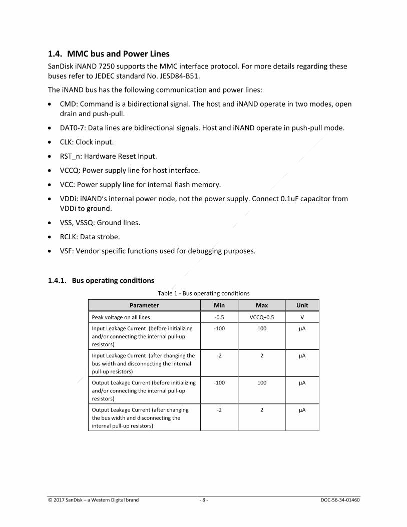
5.3.5. EXT_CSD Register
Parameter ECSD slice Description Value
S_CMD_SET [504] Supported Command Sets 1h
HPI_FEATURES [503] HPI Features 1h
BKOPS_SUPPORT [502] Background operations support 1h
MAX_PACKED_READS [501] Max packed read commands 3Fh
MAX_PACKED_WRITES [500] Max packed write commands 3Fh
DATA_TAG_SUPPORT [499] Data Tag Support 1h
TAG_UNIT_SIZE [498] Tag Unit Size 3h
TAG_RES_SIZE [497] Tag Resources Size 3h
CONTEXT_CAPABILITIES [496] Context management capabilities 5h
LARGE_UNIT_SIZE_M1 [495] Large Unit size 0h
EXT_SUPPORT [494] Extended partitions attribute support 3h
SUPPORTED_MODES [493] FFU supported modes 3h
FFU_FEATURES [492] FFU features 0h
OPERATION_CODES_TIMEO
UT
[491] Operation codes timeout
10h
FFU_ARG [490:487] FFU Argument 0h
BARRIER_SUPPORT [486] Cache barrier support 1h
CMDQ_SUPPORT [308] Command queue support 1h
CMDQ_DEPTH [307] Command queue depth 1Fh
NUMBER_OF_FW_SECTORS
_CORRECTLY_PROGRAMME
D
[305:302] Number of FW sectors correctly programmed
0h
VENDOR_PROPRIETARY_HE
ALTH_REPORT
[301:270] Vendor proprietary health report
0h
DEVICE_LIFE_TIME_EST_TYP
_B
[269] Device life time estimation type B (MLC)
1h
DEVICE_LIFE_TIME_EST_TYP
_A
[268] Device life time estimation type A (SLC)
1h
PRE_EOL_INFO [267] Pre EOL information 1h
OPTIMAL_READ_SIZE [266] Optimal read size 8h
OPTIMAL_WRITE_SIZE [265] Optimal write size 8h
OPTIMAL_TRIM_UNIT_SIZE [264] Optimal trim unit size 8h
DEVICE_VERSION [263:262] Device version 5025h
FIRMWARE_VERSION [261:254] Firmware version FW Version
PWR_CL_DDR_200_360 [253] Power class for 200MHz, DDR at VCC= 3.6V DDh
CACHE_SIZE [252:249] Cache size 1000h
GENERIC_CMD6_TIME [248] Generic CMD6 timeout 19h
POWER_OFF_LONG_TIME [247] Power off notification(long) timeout 19h
BKOPS_STATUS [246] Background operations status Default = 0h
© 2017 SanDisk – a Western Digital brand - 27 - DOC-56-34-01460
Parameter ECSD slice Description Value
CORRECTLY_PRG_SECTORS_
NUM
[245:242] Number of correctly programmed sectors
Default = 0h
INI_TIMEOUT_AP [241] 1st Initialization time after partitioning 5Ah
CACHE_FLUSH_POLICY [240] Cache Flush Policy 1h
PWR_CL_DDR_52_360 [239] Power class for 52MHz, DDR at VCC = 3.6V 0h
PWR_CL_DDR_52_195 [238] Power class for 52MHz, DDR at VCC = 1.95V DDh
PWR_CL_200_195 [237] Power class for 200MHz at VCCQ =1.95V, VCC =
3.6V DDh
PWR_CL_200_130 [236] Power class for 200MHz, at VCCQ =1.3V, VCC =
3.6V 0h
MIN_PERF_DDR_W_8_52 [235] Minimum Write Performance for 8bit at 52MHz in
DDR mode 0h
MIN_PERF_DDR_R_8_52
[234] Minimum Read Performance for 8bit at 52MHz in
DDR mode 0h
TRIM _MULT [232] TRIM Multiplier 3h
SEC_FEATURE_SUPPORT [231] Secure Feature support 55h
SEC_ERASE_MULT [230] Secure Erase Multiplier A6h
SEC_TRIM_MULT [229] Secure TRIM Multiplier A6h
BOOT_INFO [228] Boot Information 7h
BOOT_SIZE_MULT [226] Boot partition size 20h
ACCESS_SIZE [225] Access size 8h
HC_ERASE_GROUP_SIZE [224] High Capacity Erase unit size 1h (see WP group size table
below)
ERASE_TIMEOUT_MULT [223] High capacity erase time out 3h
REL_WR_SEC_C [222] Reliable write sector count 1h
HC_WP_GRP_SIZE [221] High capacity write protect group size 10h (see WP group size table
below)
S_C_VCC [220] Sleep current [VCC] 8GB – 5h
16GB – 6h
32GB – 7h
64GB – 8h
S_C_VCCQ [219] Sleep current [VCCQ] 7h
PRODUCTION_STATE_AWAR
ENESS_TIMEOUT
[218] Production state awareness timeout
17h
S_A_TIMEOUT [217] Sleep/Awake time out 12h
SLEEP_NOTIFICATION_TIME [216] Sleep notification timeout 17h
SEC_COUNT [215:212] Sector count See exported capacity table
below
SECURE_WP_INFO [211] Secure Write Protect Info 1h
MIN_PERF_W_8_52 [210] Minimum Write Performance for 8bit @52MHz Ah
MIN_PERF_R_8_52 [209] Minimum Read Performance for 8bit @52MHz Ah

© 2017 SanDisk – a Western Digital brand - 28 - DOC-56-34-01460
Parameter ECSD slice Description Value
MIN_PERF_W_8_26_4_52 [208] Minimum Write Performance for 4bit @52MHz or
8bit @26MHz Ah
MIN_PERF_R_8_26_4_52 [207] Minimum Read Performance for 4bit @52MHz or
8bit @26MHz Ah
MIN_PERF_W_4_26 [206] Minimum Write Performance for 4bit @26MHz Ah
MIN_PERF_R_4_26 [205] Minimum Read Performance for 4bit @26MHz Ah
PWR_CL_26_360 [203] Power Class for 26MHz @ 3.6V 0h
PWR_CL_52_360 [202] Power Class for 52MHz @ 3.6V 0h
PWR_CL_26_195 [201] Power Class for 26MHz @ 1.95V DDh
PWR_CL_52_195 [200] Power Class for 52MHz @ 1.95V 0h
PARTITION_SWITCH_TIME [199] Partition switching timing 3h
OUT_OF_INTERRUPT_TIME [198] Out-of-interrupt busy timing 19h
DRIVER_STRENGTH [197] I/O Driver Strength 1Fh
CARD_TYPE [196:195] Card Type 57h
CSD_STRUCTURE [194] CSD Structure Version 2h
EXT_CSD_REV [192] Extended CSD Revision 8h
CMD_SET [191] Command Set Default = 0h
Updated in runtime
CMD_SET_REV [189] Command Set Revision 0h
POWER_CLASS [187] Power Class Dh
HS_TIMING [185] High Speed Interface Timing Default = 0h
Updated in runtime by the host
DATA_STRB_MODE_SUPPOR
T
[184] Data strobe mode support 1h
BUS_WIDTH [183] Bus Width Mode Default = 0h
Updated in runtime by the host
ERASE_MEM_CONT [181] Content of explicit erased memory range 0h
PARTITION_CONFIG [179] Partition Configuration Default = 0h
Updated in runtime by the host
BOOT_CONFIG_PROT [178] Boot config protection Default = 0h
Updated in runtime by the host
BOOT_BUS_CONDITIONS [177] Boot bus width1 Default = 0h
Updated in runtime by the host
ERASE_GROUP_DEF [175] High-density erase group definition Default = 0h
Updated in runtime by the host
BOOT_WP_STATUS [174] Boot write protection status registers Default = 0h
Updated in runtime
BOOT_WP [173] Boot area write protect register 0h
USER_WP [171] User area write protect register 0h
FW_CONFIG [169] FW Configuration 0h

© 2017 SanDisk – a Western Digital brand - 29 - DOC-56-34-01460
Parameter ECSD slice Description Value
RPMB_SIZE_MULT [168] RPMB Size 20h
WR_REL_SET [167] Write reliability setting register 1Fh
WR_REL_PARAM [166] Write reliability parameter register 15h
SANITIZE_START [165] Start Sanitize operation Default = 0h
Updated in runtime by the host
BKOPS_START [164] Manually start background operations Default = 0h
Updated in runtime by the host
BKOPS_EN [163] Enable background operations handshake 2h
RST_n_FUNCTION [162] H/W reset function Default = 0h
Updated by the host
HPI_MGMT [161] HPI management Default = 0h
Updated by the host
PARTITIONING SUPPORT [160] Partitioning support 7h
MAX_ENH_SIZE_MULT [159:157] Max Enhanced Area Size 8GB – 1B5h
16GB – 383h
32GB – 702h
64GB – E1Ch
PARTITIONS_ATTRIBUTE [156] Partitions Attribute Default = 0h
Updated by the host
PARTITION_SETTING_
COMPLETED
[155] Partitioning Setting Default = 0h
Updated by the host
GP_SIZE_MULT [154:143] General Purpose Partition Size (GP4) 0h
GP_SIZE_MULT [151:149] General Purpose Partition Size (GP3) 0h
GP_SIZE_MULT [148:146] General Purpose Partition Size (GP2) 0h
GP_SIZE_MULT [145:143] General Purpose Partition Size (GP1) 0h
ENH_SIZE_MULT [142:140] Enhanced User Data Area Size 0h
ENH_START_ADDR [139:136] Enhanced User Data Start Address 0h
SEC_BAD_BLK_MGMNT [134] Bad Block Management mode 0h
PRODUCTION_STATE_AWAR
ENESS
[133] Production state awareness
0h
TCASE_SUPPORT [132] Package Case Temperature is controlled 0h
PERIODIC_WAKEUP [131] Periodic Wake-up 0h
PROGRAM_CID_CSD_DDR_S
UPPORT
[130] Program CID/CSD in DDR mode support 1h
VENDOR_SPECIFIC_FIELD [127:87] Vendor Specific Fields Reserved
PWR_CL_DDR_266 [86] Maximum power class for HS533 0h
CARD_TYPE_2ND_INDEX [84] Device HS533 support 0h
SKU_FEATURES_ID [83] 7250 SKU identification 3h
VENDOR_SPECIFIC_FIELD [82:64] Vendor Specific Fields Reserved

© 2017 SanDisk – a Western Digital brand - 30 - DOC-56-34-01460
Parameter ECSD slice Description Value
NATIVE_SECTOR_SIZE [63] Native sector size 0h
USE_NATIVE_SECTOR [62] Sector size emulation 0h
DATA_SECTOR_SIZE [61] Sector size 0h
INI_TIMEOUT_EMU [60] 1st initialization after disabling sector size
emulation
Ah
CLASS_6_CTRL [59] Class 6 commands control 0h
DYNCAP_NEEDED [58] Number of addressed group to be Released 0h
EXCEPTION_EVENTS_CTRL [57:56] Exception events control 0h
EXCEPTION_EVENTS_STATU
S
[55:54] Exception events status 0h
EXT_PARTITIONS_ATTRIBUT
E
[53:52] Extended Partitions Attribute 0h
CONTEXT_CONF [51:37] Context configuration Default = 0h
PACKED_COMMAND_STATU
S
[36] Packed command status Default = 0h
Updated in runtime
PACKED_FAILURE_INDEX [35] Packed command failure index Default = 0h
Updated in runtime
POWER_OFF_NOTIFICATION [34] Power Off Notification Default = 0h
Updated in runtime by the host
CACHE_CTRL [33] Control to turn the Cache ON/OFF 0h
FLUSH_CACHE [32] Flushing of the cache 0h
BARRIER_CTRL [31] Cache barrier 0h
MODE_CONFIG [30] Mode config 0h
MODE_OPERATION_CODES [29] Mode operation codes 0h
FFU_STATUS [26] FFU status 0h
PRE_LOADING_DATA_SIZE [25:22] Pre loading data size 0h
MAX_PRE_LOADING_DATA_
SIZE
[21:18] Max pre loading data size See Max Preloading size table
below
PRODUCT_STATE_AWARENE
SS_ENABLEMENT
[17] Product state awareness enablement 3h AUTO_PRE_SOLDERING
SECURE_REMOVAL_TYPE [16] Secure Removal Type 8h
CMDQ_MODE_EN [15] Command queue 0h

© 2017 SanDisk – a Western Digital brand - 31 - DOC-56-34-01460
5.4. User Density
The following table shows the capacity available for user data for the different device sizes:
Table 13 - Capacity for user data
Table 14 - Write protect group size
The max preloading image in iNAND 7250 is up to the exported capacity per table below
Table 15 - Max Preloading Data Size
Capacity LBA [Hex]
8GB 0xE90E80
16GB 0x1D5A000
32GB 0x3A3E000
64GB 0x7670000
Capacity HC_ERASE_GROUP_SIZE HC_WP_GRP_SIZE Erase Unit Size [MB] Write Protect Group Size [MB]
8GB 0x1 0x10 0.5MB 8MB
16GB 0x1 0x10 0.5MB 8MB
32GB 0x1 0x10 0.5MB 8MB
64GB 0x1 0x10 0.5MB 8MB
Capacity Max preloading Image size (in LBA HEX)
8GB 0xE90E80
16GB 0x1D5A000
32GB 0x3A3E000
64GB 0x7670000

© 2017 SanDisk – a Western Digital brand - 32 - DOC-56-34-01460
6. HW APPLICATION GUIDELINES
6.1. Design Guidelines
The e.MMC specification enforces single device per host channel; multi-device configuration per a single host channel is not supported.
CLK, RCLK(DS), CMD and DATx lines should be connected to respected host signals. The e.MMC specification requires that all signals will be connected point-to-point, i.e. a single e.MMC device per host channel.
All power supply and ground pads must be connected.
Make sure pull-up resistors are placed on schematic in case these are external. For further details please refer to “Table 19 - Pull-ups Definition”
Bypass capacitors shall be placed as close to the e.MMC device as possible; normally it is recommended to have 0.1uF and 4.7uF capacitors per power supply rail, though specific designs may include a different configuration in which there are more than two capacitors:
o VCC and VCCQ slew rates shall be minimally affected by any bypass capacitors configuration
o It is recommended to verify the bypass capacitors requirement in the product data sheet
VDDi bypass capacitor shall be placed on the PCB. The VDDi is an internal power node for the controller and requires capacitor in range 0.1uF – 2.2uF connected between VDDi pad and ground
Vendor Specific Function (VSF) pins should be connected to accessible test points on the PCB (TP on schematic below). It’s recommended to have accessible ground (GND) pads near each TP on PCB
It is recommended to layout e.MMC signals with controlled impedance of 45-55 Ohm referencing to adjusted ground plane

© 2017 SanDisk – a Western Digital brand - 33 - DOC-56-34-01460
6.2. Capacitor Selection & Layout Guidelines SanDisk iNAND 7250 has three power domains assigned to VCCQ, VCC and VDDi, as shown in table below.
Table 16 - 7250 Power Domains
Pin Power Domain Comments
VCCQ Host Interface Supported voltage ranges: Low Voltage Region: 1.8V (nominal)
VCC Memory Supported voltage range: High Voltage Region: 3.3V (nominal)
VDDi Internal VDDi is the internal regulator connection to an external decoupling capacitor.
It is recommended that the power domains connectivity will follow figure 4:
Capacitor C_5: Capacitor >= 0.1uF Capacitor =< 2.2uF X5R or X7R Voltage > 6.3V
Trace Requirements: Resistance < 0.5[Ω] Inductance < 3n[Hy]
Placement: Closest to ball C2
C_5 NC
DAT3
DAT4
DAT5
DAT6
DAT7
NC
NC
NC
NC
NC
NC
NC
NC
NC
Vddi
NC
VssQ
NC
VccQ
NC
NC
NC
NC
NC
NC
NC
NC
NC
NC
NC
NC
NC
NC
NC
NC
NC
VCC
VSS
NC
VSF1
VSF2
NC
NC
NC
NC
NC
NC
VCC
VSF3
NC
NC
NC
NC
NC
NC
VSS
NC
NC
NC
NC
NC
NC
NC
RCLK
VSS
NC
NC
NC
NC
NC
NC
VSS
VCC
NC
NC
NC
NC
NC
NC
RESET
VSF4
NC
NC
NC
NC
NC
NC
NC
NC
NC
NC
NC
NC
VccQ
CMD
CLK
NC
NC
NC
NC
NC
NC
NC
NC
NC
VssQ
NC
VccQ
VssQ
NC
NC
NC
NC
NC
NC
NC
NC
NC
NC
NC
VccQ
VssQ
VccQ
VssQ
NC
NC
NC
NC
NC
NC
NC
NC
NC
NC
DAT0
DAT1
DAT2
VSS
NC
NC
NC
NC
NC
NC
NC
NC
AA BB CC DD EE FF GG HH JJ KK LL MM NN PP
99
1010
11
22
33
44
55
66
77
88
1111
1212
1313
1414 NC
NC
NC
VSS
VCC
C_3 C_4
Top View
Capacitor C_3/4: Capacitor C3 >= 4.7uF Capacitor C4 =< 0.1uF X5R or X7R Voltage > 6.3V
Trace Requirements: Resistance < 0.5[Ω] Inductance < 3n[Hy]
Placement: Closest to ball F5
C_1 C_2
Capacitor C_1/2: Capacitor C1 >= 4.7uF Capacitor C2 =< 0.1uF X5R or X7R Voltage > 6.3V
Trace Requirements: Resistance < 0.5[Ω] Inductance < 3n[Hy]
Placement: Closest to ball P3
QRDY
Figure 4 - Recommended Power Domain Connectivity
Note: Signal routing in the diagram is for illustration purposes only and the final routing depends final PCB layout.
For clarity, the diagram does not include VSS connection. All balls marked VSS shall be connected to a ground (GND) plane.

© 2017 SanDisk – a Western Digital brand - 34 - DOC-56-34-01460
It is recommended to use a X5R/X7R SMT-Ceramic capacitors rated for 6.3V/10V with footprint of 0402 or above.
When using ceramic capacitor, it should be located as close to the supply ball as possible. This will eliminate mounting inductance effects and give the internal IC rail a cleaner voltage supply
Make all of the power (high current) traces as short, direct, and thick as possible. The capacitors should be as close to each other as possible, as it reduces EMI radiated by the power traces due to the high switching currents through them. In addition, it shall also reduce mounting inductance and resistance as well, which in turn reduces noise spikes, ringing, and IR drop which produce voltage errors.
The grounds of the IC capacitors should be connected close together directly to a ground plane. It is also recommended to have a ground plane on both sides of the PCB, as it reduces noise by reducing ground loop.
The loop inductance per capacitor shall not exceed 3nH (both on VCC/VCCQ & VSS/VSSQ loops).
Cin2 shall be placed closer (from both distance & inductance POV) to the iNAND power & ground balls.
Multiple via connections are recommended per each capacitor pad. It is recommended to place the power and ground vias of the capacitor as close to each other as possible.
On test platforms, where the iNAND socket is in use, the loop inductance per capacitor shall not exceed 5nH (both on VCC/VCCQ & VSS/VSSQ loop).
No passives should be placed below the iNAND device (between iNAND & PCB).
VSF balls (VSF1/4) should have exposed and floated test pads on the PCB, with near exposed GND for better measurement.
Signal Traces:
Data, CMD, CLK & RCLK bus trace length mismatch should be minimal (up to +/-1mm). Traces should be45-55 ohm controlled impedance.

© 2017 SanDisk – a Western Digital brand - 35 - DOC-56-34-01460
6.3. Reference Schematics
Figure 5 – e.MMC Reference Schematics
Table 17 – Pull-ups Definition
Parameter Symbol Min Typ Max Unit Remark
Pull-up resistance for DAT0–7 RDAT 10 100(1)
Kohm to prevent bus floating
Pull-up resistance for CMD RCMD 4.7 100(1)
Kohm to prevent bus floating
Pull-down resistance for Data Strobe (RCLK)
RPD 10 47 Kohm At HS400 mode
(1) Recommended maximum pull-up is 50Kohm for 1.8V interface supply voltages. A 3V part may use the whole range up to 100Kohms
Recommended capacitors:
CAPACITOR VALUE MANUFACTURER MANUFACTURER P/N
4.7uF MURATA GRM185R60J475ME15D
TAIYO YUDEN JMK107BJ475MK-T
0.1uF MURATA GRM155R71A104KA01D
KYOCERA CM05X5R104K06AH
2.2uF PANASONIC ECJ0EB0J225M
SAMSUNG CL05A225MQ5NSNC

© 2017 SanDisk – a Western Digital brand - 36 - DOC-56-34-01460
7. PROPRIETY INAND 7250 FEATURE OVERVIEW
7.1. Smart Partitioning
The Industrial iNAND 7250 supports the ability to be partitioned by the host into several areas with varying endurance, retention, and security features and characteristics. The 7250 partitioning implementation physically creates the separation inside the device. These separate pools are individually managed, allowing for independent wear leveling, refresh, and health reporting schemes. This also protects each partition from any unwanted effects of unintended use of other partitions. For example, overuse of a write intensive partition would not affect an operating system partition.
Please reference the “iNAND 7250 Partitioning” application note for more information.
7.2. Manual Refresh
The Industrial iNAND 7250 is designed with an automatic read refresh capability. The sophisticated read refresh algorithms provide protection from the effects of read disturb, read endurance and data retention issues.
In addition, the iNAND 7250 provides the ability for the host to force a refresh of designated blocks. The host can initiate, restart and monitor the progress of the refresh activity.
To initiate a refresh: Send CMD62 with argument of 0xAEFE1430 To check refresh progress: Send CMD62 with argument of 0xAEFE1431, then send
CMD63 with argument 0x00000000 to retrieve the progress in terms of percentage of the entire device refreshed
To reset the refresh to the beginning of the device: Send CMD62 with argument of 0xAEFE1432
Please reference the “iNAND 7250 Manual Refresh” application note for more information.
7.3. Boot & RPMB resize
The Industrial iNAND 7250 allows for larger boot (up to 31.875 MB) and RPMB (up to 16 MB) partitions than specified in the standards. To accomplish this, a vendor specific command (CMD62) has been defined. To accomplish this perform the following steps:
To indicate resize operation: Send CMD62 with argument of 0x254DDEC4 To set boot size: Send CMD62 with argument BOOT_SIZE_MULT as defined by the
JEDEC spec To set RPMB size: Send CMD62 with argument RPMB_SIZE_MULT as defined by the
JEDEC spec Power-on/reset is required for this change to take effect
Please reference the “iNAND 7250 Partitioning” application note for more information.

© 2017 SanDisk – a Western Digital brand - 37 - DOC-56-34-01460
7.4. One Time Programmable Register for Custom ID
The Industrial iNAND 7250 allows customers to set a custom one-time programmable string as part of the vendor specific fields in the ext_CSD
The unique 8 byte Custom ID is specified in EXT_CSD[71-64] Each byte must be written individually using the SWITCH command (CMD6) These bytes may only be written once
7.5. Device Report & Advanced Health Status
The Industrial iNAND 7250 Device Report feature reflects the firmware and device status. In addition to the Device Report, iNAND 7250 introduces a new proprietary Advanced Health Status feature that reflects more information on the device health and temperature.
Enabling Device Report Mode: Send CMD62 with argument of 0x96C9D71C - R1b Response will be returned
Reading Device Report Data: Once the host enters Device Report mode, CMD63 with argument 0x00000000 will retrieve the report - 512 Bytes will be returned to the host (Note: CMD63 behaves similarly to CMD17)
Resume Normal Operation Mode: Once the Device Report read command (CMD63) was completed, the device automatically goes out of Device Report mode, and resumes normal operation mode
7.5.1. Device Report fields
Byte
Offset
Size
(Bytes)
Field Comments
[3:0] 4 Avg Erase Count System Average erase value across all system blocks
[4:7] 4 Reserved
[8:11] 4 Avg Erase Count MLC Average erase value across all MLC blocks
[15:12] 4 Read Reclaim Count System Number of reads of system data which passed read-scrub thresholds
and require reclaim
[19:16] 4 Reserved
[23:20] 4 Read Reclaim Count MLC Number of MLC reads which passed read-scrub thresholds and require
reclaim
[27:24] 4 Bad Block Manufacturer Total bad blocks detected during manufacturing process
[31:28] 4 Bad Block Runtime System Total bad blocks in system partitions detected during run-time
[35:32] 4 Reserved
[39:36] 4 Bad Block Runtime MLC Total bad blocks in MLC partition detected during run-time
[43:40] 4 Patch Trial Count Number of secure field firmware updates (sFFU) done from the
beginning of the device life
[55:44] 12 Patch Release Date Current sFFU release date
[63:56] 8 Patch Release Time Current sFFU release hour
[67:64] 4 Cumulative Write Data Size In
100MB Total bytes written from the host in multiples of 100 MB

© 2017 SanDisk – a Western Digital brand - 38 - DOC-56-34-01460
[71:68] 4 VCC Voltage Drop Occurrences
Number of ungraceful power downs to the device. Counter may be
inaccurate due to uncommitted counter updates during repeated
voltage drops .
[75:72] 4 VCC Voltage Droop Occurrences Number of power-droops (slight power-droop below a threshold and
for a very short period of time)
[79:76] 4 Failures to Recover New Host Data
After Power Loss Counts times new host data is discarded due to power loss
[83:80] 4 Recovery Operations After Voltage
Droop
Number of recovery operations done by the device while power-droop
detected
[99:84] 16 Reserved
7.5.2. Advanced Health Status Fields
Byte Offset Size
(Bytes)
Field Comments
[103:100] 4 Cumulative Initialization Count Number of power-ups
[107:104] 4 Max Erase Count System Maximum erase value among all system blocks
[111:108] 4 Reserved
[115:112] 4 Max Erase Count MLC Maximum erase value among all MLC blocks
[119:116] 4 Min Erase Count System Minimum erase value among all system blocks
[123:120] 4 Reserved
[127:124] 4 Min Erase Count MLC Minimum erase value among all MLC blocks
[131:128] 4 Max Erase Count EUDA Maximum erase value among any EUDA blocks
[135:132] 4 Min Erase Count EUDA Minimum erase value among any EUDA blocks
[139:136] 4 Avg Erase Count EUDA Average erase value among any EUDA blocks
[143:140] 4 Read Reclaim Count EUDA Number of reads of EUDA data which passed read-scrub thresholds and
require reclaim
[147:144] 4 Bad Block Runtime EUDA Total bad blocks in EUDA partition detected during run-time
[151:148] 4 Pre EOL State EUDA
Pre EOL levels EUDA blocks: 1: normal 2: warning 3: urgent 4: read only
[155:152] 4 Pre EOL State System
Pre EOL levels system blocks: 1: normal 2: warning 3: urgent 4: read only
[159:156] 4 Pre EOL State MLC
Pre EOL levels blocks, remainder of device: 1: normal 2: warning 3: urgent 4: read only
[163:160] 4 Uncorrectable Error Correction
Code Number of uncorrectable errors detected
[167:164] 4 Current Temperature The current temperature of the device, in degrees Celsius
[171:168] 4 Min Temperature Minimum temperature recorded in the device over lifetime, in degrees
Celsius

© 2017 SanDisk – a Western Digital brand - 39 - DOC-56-34-01460
[175:172] 4 Max Temperature Maximum temperature recorded in the device over lifetime, in degrees
Celsius
[179:176] 4 Health Device Level EUDA Health status of EUDA blocks, 1–100%
[183:180] 4 Health Device Level System Health status of system blocks, 1–100%
[187:184] 4 Health Device Level MLC Health status of remainder of device blocks, 1–100% The worst case between intermediate storage and MLC pools.
[511:188] 324 Reserved
7.6. Power-Loss indications
Industrial iNAND 7250 is also serving the host by notifying him on cases of Power-Loss events and internal handling of those events. A dedicated field in the EXT_CSD register was allocated to indicate the occurrence of Power Loss/Write Abort during the last power down. This field reports if a Power Loss was detected and recovered during the last power-up. In order to retrieve this field, the host should issue CMD8 command – SEND_EXT_CSD. This command returns full EXT_CSD structure – 512 bytes as block of data. Following is the EXT_CSD field details: Name Field Size (bytes) Cell Type Hex Offset Dec. Offset
Power Loss indication POWER_LOSS_REPORT 1 R 0x79 121
POWER_LOSS_REPORT[121] details: Bit[2]: RECOVERY_SUCCESS
0x1: Recovery passed successfully 0x0: Recovery failed
Bit[1]: RECOVER_OLD_DATA 0x1: Recovery to old copy of data 0x0: No data recovery required
Bit[0]: POWER_LOSS_DETECTED 0x1: Unexpected Power Loss was detected - Detection is done during initialization, immediately after Power-Up
Note: In case Power Loss did not occur on last shut down, this register will show 0x00
7.6.1. Unstable Power-Supply indications
In case of Flash voltage drop, the iNAND may not be able to recover the data that was already transferred to the iNAND device, but wasn’t committed in the Flash. In this case the iNAND will “abort” the current host write and return back to the host with an error indication.
iNAND 7250 will use BIT19 and BIT20 (cc_error) in the command response to indicate VDET error status to the host. the VDET error indication can be seen only if CMD13 was issued, or in the next command response.
Examples: Open Mode (CMD25+CMD12+CMD13):
In both cases, where the voltage droop occurs before or after CMD12:

© 2017 SanDisk – a Western Digital brand - 40 - DOC-56-34-01460
CMD12 response will not have BIT19 and BIT20 set. CMD13 will identify the error indication - BIT19 and BIT20 will be set in CMD13 response Note: The host may send many CMD13 and the BIT19 will be set only in first CMD13 after releasing the busy.
Close Mode (CMD23+CMD25+CMD13): CMD13 will identify the error indication - BIT19 and BIT20 will be set in CMD13 response
Single Block Mode (CMD24+CMD13): CMD13 will identify the error indication - BIT19 and BIT20 will be set in CMD13 response
Host shall retry latest command as long as the VDET error indication on CMD13 response (or next command response (BIT19 and BIT20 are set) is still set

© 2017 SanDisk – a Western Digital brand - 41 - DOC-56-34-01460
8. MARKING First row: Simplified SanDisk Logo Second row: Sales item P/N Third row: Country of origin i.e. ‘TAIWAN’ or ‘CHINA’ * No ES marking for product in mass production. Fourth row: Y- Last digit of year WW- Work week D- A day within the week. MTLLLXXX – Internal use 2D barcode: Store the 12 Digital ID information as reflected in the fourth row
Figure 7 - Product marking 8GB-64GB

© 2017 SanDisk – a Western Digital brand - 42 - DOC-56-34-01460
9. ORDERING INFORMATION Table 18 – Ordering Information (-25°C to +85°C ambient)
Previous product version for existing customers only
Capacity Technology Part Number Samples Part Number Package e.MMC
8GB 15nm X2 eMLC SDINBDG4-8G-I SDINBDG4-8G-IQ 11.5x13x0.8mm 5.1
16GB 15nm X2 eMLC SDINBDG4-16G-I SDINBDG4-16G-IQ 11.5x13x0.8mm 5.1
32GB 15nm X2 eMLC SDINBDG4-32G-I SDINBDG4-32G-IQ 11.5x13x1.0mm 5.1
64GB 15nm X2 eMLC SDINBDG4-64G-I SDINBDG4-64G-IQ 11.5x13x1.2mm 5.1
Latest product version
Capacity Technology Part Number Samples Part Number Package e.MMC
8GB 15nm X2 eMLC SDINBDG4-8G-I1 SDINBDG4-8G-I1Q 11.5x13x0.8mm 5.1
16GB 15nm X2 eMLC SDINBDG4-16G-I1 SDINBDG4-16G-I1Q 11.5x13x0.8mm 5.1
32GB 15nm X2 eMLC SDINBDG4-32G-I1 SDINBDG4-32G-I1Q 11.5x13x1.0mm 5.1
64GB 15nm X2 eMLC SDINBDG4-64G-I1 SDINBDG4-64G-I1Q 11.5x13x1.2mm 5.1
Table 19 – Ordering Information (-40°C to +85°C ambient)
Capacity Technology Part Number Samples Part Number Package e.MMC
8GB 15nm X2 eMLC SDINBDG4-8G-XI1 SDINBDG4-8G-XI1Q 11.5x13x0.8mm 5.1
16GB 15nm X2 eMLC SDINBDG4-16G-XI1 SDINBDG4-16G-XI1Q 11.5x13x0.8mm 5.1
32GB 15nm X2 eMLC SDINBDG4-32G-XI1 SDINBDG4-32G-XI1Q 11.5x13x1.0mm 5.1
64GB 15nm X2 eMLC SDINBDG4-64G-XI1 SDINBDG4-64G-XI1Q 11.5x13x1.2mm 5.1

© 2017 SanDisk – a Western Digital brand - 43 - DOC-56-34-01460
HOW TO CONTACT US Please refer to SanDisk’s web site for contact information: www.sandisk.com
Western Digital Technologies, Inc.
951 SanDisk Dr.
Milpitas, CA 95035-7933
Phone: +1-408-801-1000 [email protected]
www.sandisk.com


![LBT-HS400 V01a-1 [更新済み]Title LBT-HS400_V01a-1 [更新済み] Created Date 4/12/2011 1:00:25 PM](https://img.pdfslide.us/doc/110x75/5e7a9150e93a8c2e9233e3f5/lbt-hs400-v01a-1-title-lbt-hs400v01a-1-created-date.jpg)