Embed Size (px)
Citation preview
Data Device Corporation
Multi-Protocol Data Bus Interface
NHi-ET Enhanced TerminalsBus Controller, Remote Terminal, Bus Monitor
User's Manual
Version 2014.01.09January 2014
The information provided in this document is believed to be accurate; however, no responsibility is assumed by Data Device Corporationfor its use, and no license or rights are granted by implication or otherwise in connection therewith. Specificationsare subject to change without notice.
105 Wilbur Place, Bohemia, NY 117161-800-DDC-5757 | 631-567-5600
[email protected] | www.ddc-web.com
- -1
TABLE OF CONTENTS
1.0.0 SCOPE. . . . . . . . 62.0.0 NHi-ET PROTOCOL COMPLIANCE . . . . 63.0.0 INTRODUCTION . . . . . . 63.1.0 FEATURES . . . . . . . 63.1.1 GENERAL FEATURES . . . . . 63.1.2 BUS CONTROLLER HIGHLIGHTS . . . . 73.1.3 REMOTE TERMINAL HIGHLIGHTS . . . . 73.14 BUS MONITOR HIGHLIGHTS . . . . . 83.2.0 BLOCK DIAGRAM . . . . . . 93.3.0 PROTOCOL CHIP DESCRIPTION . . . . 103.3.1 HOST BUS INTERFACE UNIT . . . . . 103.3.2 I/O BUS INTERFACE UNIT . . . . . 103.3.3 INTERRUPT CONTROL UNIT . . . . . 103.3.3.1 ICU REGISTERS . . . . . . 103.3.3.1.1 INTERRUPT DEFINITION TABLE . . . . 113.3.3.2 ICU FIFO . . . . . . . 113.3.4 DUAL REDUNDANT FRONT END . . . . 123.3.4.1 MANCHESTER DECODER . . . . . 123.3.4.2 MANCHESTER ENCODER . . . . . 123.3.4.3 GAP COUNTER . . . . . . 123.3.4.4 RT - RT NO RESPONSE COUNTER . . . . 123.3.4.5 MINIMUM RESPONSE TIME COUNTER . . . 123.3.4.6 FAIL -SAFE TIMEOUT COUNTER . . . . 123.3.5 MESSAGE PROCESSOR UNIT . . . . 123.4.0 RT HARDWIRE TERMINAL ADDRESS. . . . 134.0.0 DATA STRUCTURE . . . . . . 134.1.0 ADDRESS MAP . . . . . . 134.2.0 INTERNAL REGISTERS . . . . . 144.2.1 CONTROL . . . . . . . 154.2.2 POINTER TABLE ADDRESS . . . . . 164.2.3 BASIC STATUS . . . . . . 174.2.4 INTERRUPT REQUEST . . . . . 184.2.5 INTERRUPT MASK . . . . . . 184.2.6 INTERRUPT VECTOR . . . . . . 184.2.7 CONFIGURATION REGISTER 2 . . . . 194.2.8 AUXILIARY VECTOR REGISTER . . . . 204.2.9 REAL- TIME CLOCK . . . . . . 204.2.10 RTC CONTROL REGISTER . . . . . 214.2.11 FIFO READ . . . . . . . 224.2.12 FIFO RESET . . . . . . . 224.2.13 LAST COMMAND REGISTER . . . . . 224.2.14 LAST STATUS REGISTER . . . . . 234.2.15 RESET REMOTE TERMINAL . . . . 234.2.16 ENCODER STATUS . . . . . . 234.2.17 CONDITION REGISTER . . . . . 234.2.18 ENCODER DATA REGISTER . . . . 244.2.19 ENCODER DATA TRANSMIT RQST . . . . 244.2.20 ENCODER COMMAND TRANSMIT REQUEST . . 244.2.21 EXTERNAL TERMINAL ADDRESS REGISTER . . 254.2.22 COMMAND OUTPUT PINS . . . . . 254.2.23 I/ O TAG WORD REGISTER . . . . . 254.2.24 CONFIGURATION REGISTER 1 . . . . 26
- -2
TABLE OF CONTENTS(continued)
4.2.25 FRAME "A" POINTER; BLOCK "A" START . . . 274.2.26 FRAME "A" LENGTH; BLOCK "A" END . . . 274.2.27 FRAME "B" POINTER; BLOCK "B" START . . . 284.2.28 FRAME "B" LENGTH; BLOCK "B" END . . . 284.2.29 BC FRAME GAP; WORD MONITOR EOF OPTIONS . . 294.2.30 CONFIGURATION REGISTER 3 . . . . 304.2.31 MT ADDRESS FILTER (RT15- RT0) . . . . 314.2.32 MT ADDRESS FILTER (RT31- RT16) . . . . 314.2.33 BLOCK "A" LAST ADDRESS . . . . . 314.2.34 BLOCK "B" LAST ADDRESS . . . . . 324.3.0 RT DATA TABLES . . . . . . 324.3.1 MESSAGE ILLEGALITY . . . . . 334.3.2 DATA TABLE TAG WORD . . . . . 334.3.3 DATA TABLE POINTER . . . . . 344.3.4 RT DATA TABLE BUFFERING SCHEME . . . 354.3.4.1 RT RAM ACCESS . . . . . . 354.3.4.2 HOST RAM ACCESS . . . . . . 354.3.4.3 READ- MODIFY- WRITE . . . . . 364.4.4.0 BC MESSAGE LISTS AND DATA TABLES . . . 364.4.1 BC CONTROL WORD . . . . . . 374.4.2 BC COMMAND WORD. . . . . . 394.4.3 BC MESSAGE GAP WORD . . . . . 394.4.4 BC TIME TAG MS WORD . . . . . 404.4.5 BC TIME TAG LS WORD . . . . . 404.4.6 BC DATA WORD . . . . . . 404.4.7 BC STATUS RESPONSE . . . . . 404.4.8 BC MESSAGES . . . . . . 404.5.0 MESSAGE MONITOR MESSAGE LISTS AND DATA . .
TABLES42
4.5.1 MESSAGE MONITOR TAG WORD . . . . 424.5.2 MESSAGE MONITOR COMMAND/STATUS WORD . . 434.5.3 MESSAGE MONITOR TIME TAG MS WORD . . . 434.5.4 MESSAGE MONITOR TIME TAG LS WORD . . . 434.5.5 MESSAGE MONITOR DATA WORDS . . . . 434.5.6 MESSAGE MONITOR MESSAGE TABLE FORMATS . . 444.6.0 WORD MONITOR DATA TABLES . . . . 444.6.1 WORD MONITOR TAG WORD . . . . . 454.6.2 WORD MONITOR COMMAND / STATUS - DATA . . 464.6.3 WORD MONITOR TIME TAG MS WORD . . . 464.6.4 WORD MONITOR TIME TAG LS WORD . . . 465.0.0 RT MODE CODE OPERATION . . . . . 465.1.0 GENERAL . . . . . . . 465.2.0 TABLE OF RT MODE CODE RESPONSES . . . 475.2.1 DYNAMIC BUS CONTROL (00000; T/R=1) . . . 475.2.2 SYNCHRONIZE WITHOUT DATA (00001; T/R=1) . . 475.2.3 TRANSMIT LAST STATUS WORD (00010; T/R=1) . . 485.2.4 INITIATE SELF TEST (00011; T/R=1) . . . . 485.2.5 TRANSMITTER SHUTDOWN (00100; T/R=1) . . 48
- -3
TABLE OF CONTENTS(continued)
5.2.6 OVERRIDE TRANSMITTER SHUTDOWN . . . (00101; T/R=1)
49
5.2.7 INHIBIT TERMINAL FLAG (00110; T/R=1) . . . 495.2.8 OVERRIDE INHIBIT TERMINAL FLAG (00110; T/R=1) . . 495.2.9 RESET REMOTE TERMINAL (01000; T/ R= 1) . . . 505.2.10 RESERVED MODE CODES (01001- 01111; T/ R= 1) . . 505.2.11 TRANSMIT VECTOR WORD (10000; T/ R= 1) . . . 505.2.12 SYNCHRONIZE WITH DATA WORD (10001; T/ R= 0) . . 515.2.13 TRANSMIT LAST COMMAND (10010; T/ R= 1). . . 515.2.14 TRANSMIT BIT WORD (10011; T/ R= 1) . . . 525.2.15 SELECTED TRANSMITTER SHUTDOWN . . .
(10100; T/ R= 0)52
5.2.16 OVERRIDE SELECTED TRANSMITTER SHUTDOWN . . (10101; T/ R= 0)
53
5.2.17 RESERVED MODE CODES (10110- 11111; T/ R= 1) . . 535.2.18 RESERVED MODE CODES (10110- 11111; T/ R= 0) . . 536.0.0 INITIALIZATION . . . . . . 546.1.0 INTERNAL INITIALIZATION . . . . . 546.2.0 HOST INITIALIZATION OF NHi-ET . . . . 557.0.0 INTERRUPT HANDLING . . . . . 567.1.0 HARDWARE INTERRUPT ACKNOWLEDGE . . . 567.2.0 SOFTWARE INTERRUPT ACKNOWLEDGE . . . 578.0.0 TIPS - HINTS 'N TRICKS . . . . . 578.1.0 BUS CONTROLLER APPLICATIONS . . . . 578.1.1 BC REGISTERS . . . . . . 578.1.1.1 CONFIGURATION REG 2 . . . . . 578.1.1.2 CONFIGURATION REG 1 . . . . . 588.1.1.3 FRAME “A” POINTER . . . . . . 588.1.1.4 FRAME “A” LENGTH . . . . . . 588.1.1.5 FRAME “B” POINTER . . . . . . 588.1.1.6 FRAME “B” LENGTH . . . . . . 588.1.1.7 CONDITION REGISTER . . . . . 588.1.1.8 END OF FRAME GAP . . . . . . 588.1.1.9 CONFIGURATION REG 3 . . . . . 588.1.2 BC RAM . . . . . . . 588.1.3 BC MESSAGE TABLE . . . . . . 598.1.4 BC CONTROL WORD . . . . . . 598.1.5 BC COMMAND WORD. . . . . . 598.1.6 MESSAGE GAP WORD . . . . . 598.1.7 32 BIT TIME TAG( 2 WORDS) . . . . . 608.1.8 BC INTERRUPTS . . . . . . 608.1.9 BUS CONTROLLER EXAMPLES . . . . 608.1.10 SAMPLE BUS CONTROLLER MEMORY MAP . . . 618.2.0 MESSAGE MONITOR APPLICATIONS . . . 638.2.1 MESSAGE MONITOR REGISTERS . . . . 638.2.1.1 CONFIGURATION REG 2 . . . . . 638.2.1.2 CONFIGURATION REG 1 . . . . . 638.2.1.3 FRAME “A” POINTER . . . . . . 648.2.1.4 FRAME “A” LENGTH . . . . . . 648.2.1.5 FRAME “B” POINTER . . . . . . 648.2.1.6 FRAME “B” LENGTH . . . . . . 648.2.1.7 CONDITION REGISTER . . . . . 648.2.1.8 CONFIGURATION REGISTER 3 . . . . 64
- -4
TABLE OF CONTENTS(continued)
8.2.1.9 ADDRESS FILTER (15:0) . . . . . 648.2.1.10 ADDRESS FILTER (31:16) . . . . . 648.2.2 MESSAGE MONITOR RAM . . . . . 648.2.3 MESSAGE MONITOR MESSAGE TABLE . . . 648.2.4 MESSAGE MONITOR TAG WORD . . . . 658.2.5 COMMAND WORD OR STATUS WORD . . . 658.2.6 DATA WORD( S) . . . . . . 658.2.7 MESSAGE MONITOR EXAMPLE . . . . 658.3.0 WORD MONITOR APPLICATIONS . . . . 658.3.1 WORD MONITOR REGISTERS . . . . 668.3.1.1 CONFIGURATION REG 2 . . . . . 668.3.1.2 CONFIGURATION REG 1 . . . . . 668.3.1.3 BLOCK “A” START . . . . . . 668.3.1.4 BLOCK “A” END . . . . . . 668.3.1.5 BLOCK “B” START . . . . . . 668.3.1.6 BLOCK “B” END . . . . . . 668.3.1.7 CONDITION REGISTER . . . . . 668.3.1.8 WORD MONITOR END OF BLOCK OPTIONS . . . 678.3.1.9 CONFIGURATION REGISTER 3 . . . . 678.3.2 WORD MONITOR EXAMPLE . . . . . 678.4.0 SIMULTANEOUS MONITOR AND REMOTE TERMINAL . 678.4.1 SIMULTANEOUS MODE INTERRUPT HANDLING . . 678.5.0 PC BOARD CONSIDERATIONS AND GUIDE LINES . . 689.0.0 PIN FUNCTIONAL DESCRIPTION . . . . 689.1.0 GENERAL PURPOSE SIGNALS . . . . 699.2.0 HOST INTERFACE SIGNALS . . . . . 699.3.0 DISCRETE I/ O BUS INTERFACE SIGNALS . . . 709.4.0 MIL BUS INTERFACE SIGNALS . . . . 7110.0.0 ELECTRICAL CHARACTERISTICS . . . . 7110.1.0 ABSOLUTE MAXIMUM RATINGS . . . . 7110.2.0 OPERATING CONDITIONS . . . . . 7110.3.0 I/O TYPES & DESCRIPTIONS . . . . . 7210.4.0 I/O ELECTRICAL CHARACTERISTICS . . . 7211.0.0 TIMING DIAGRAMS . . . . . . 7311.0.1 HOST WRITE CYCLE . . . . . . 7311.0.2 HOST READ CYCLE . . . . . . 7311.0.3 HOST READ- MODIFY- WRITE CYCLE . . . 7411.0.4 RT HARDWARE INTERRUPT ACKNOWLEDGE CYCLE . 7411.0.5 I/O WRITE CYCLE . . . . . . 7511.0.6 I/O READ CYCLE . . . . . . 7511.0.7 COMMAND WRITE CYCLE . . . . . 7611.0.8 TERMINAL ADDRESS READ CYCLE . . . . 7611.0.9 SOFTWARE INTERRUPT ACKNOWLEDGE CYCLE . . 7711.0.10 TIMING DIAGRAM NOTES . . . . . 7711.1.0 TIMING PARAMETER TABLES . . . . 7811.1.1 HOST READ, WRITE; READ- MODIFY- WRITE TABLE .
SOFTWARE INTERRUPT ACKNOWLEDGE78
11.1.2 I/O READ and TERMINAL ADDRESS READ TABLE . . 7811.1.3 I/O WRITE and COMMAND WRITE TABLE . . . 7811.1.4 HARDWARE INTERRUPT ACKNOWLEDGE TABLE . . 79
- -5
TABLE OF CONTENTS(continued)
12.0.0 PIN FUNCTIONS . . . . . . 8012.1.0 GENERIC PACKAGE OUTLINE DRAWINGS . . . 8112.1.1 QUAD FLAT PACK UNFORMED LEADS . . . 8112.1.2 QUAD FLAT PACK GULL WING LEADS . . . 8112.1.3 PIN GRID ARRAY . . . . . . 8212.1.4 MICRO QUAD FLAT PACK UNFORMED LEADS . . 8312.1.5 MICRO QUAD FLAT PACK GULL WING LEADS . . 8313.0.0 MATING TRANSFORMER REFERENCE . . . 8414.0.0 ORDERING INFORMATION . . . . . 85
- -6
1.0.0 SCOPEThis document defines the functional and electrical specification for National Hybrid'sseries of MIL- STD- Data Bus Enhanced Terminals (NHi- ET).
2.0.0 NHi-ET PROTOCOL COMPLIANCE
MIL- STD- 1553AMIL- STD- 1553B Notices I and IIMIL- STD- 1760BMCAIR MDC A3818, A5690, A4905, A5332EFA/ STANAG- 3838 requirements for Eurofighter Aircraft
3.0.0 INTRODUCTIONThe NHi- ET is a low cost complete Multi-Protocol Mil- Std- Data Bus Interface between a dualredundant bus and a host processor. The device functions as a programmable Bus Controller,Remote Terminal, and Bus Monitor containing a protocol chip, two +5V monolithic transceiversand 16K or 64K word SRAM. The unit is available packaged in a 1.1" x 1.1" 69 pin ceramicPGA, or 1.1" x 1.1" 68 pin ceramic quad flatpack. The only external components required are twocoupling transformers.
The NHi- ET appears to the host computer as 16K or 64K words of 16 bit wide memory controlledby standard RAM signals. The device can thus be easily interfaced with all popular processorsand buses. The built in interrupt controller supports an internal FIFO which retains headerinformation for queuing up to 6 pending interrupt requests plus an overflow interrupt.
All modes of operation access data tables via pointers residing in RAM which facilitates multiplebuffering. This allows buffers to change without moving data and promotes efficient use of RAMspace. The data tables have programmable sizes and locations.
The NHi-ET is plug in compatible with the popular NHi-RT family of remote terminal with nochanges to hardware or software required. The NHi-ET defaults to the NHi-RT remote terminaloperation on power up.
3.1.0 FEATURESThe NHi- ET is form, fit, and function compatible to the NHi- RT series of parts. This interchangeability gives the user a high degree of flexibility when configuring a system around the NHi familyof parts.
3.1.1 GENERAL FEATURES•Mulit-Protocol Interface•Single +5 volt supply.•Operates from 10 Mhz clock.•Contains two monolithic +5V transceivers•Appears to host as a Dual Port Double Buffered 16K or 64K x 16 SRAM•Footprint less than 1.25 square inches•Ensures integrity of all shared data and control structures•Built- in interrupt controller•Internal FIFO is configurable to retain header information for queuing up to 6 pending interrupt requests plus an overflow interrupt, or as a 7 interrupt revolving FIFO•Provides interrupt priority input and output pins for daisy- chaining interrupt requests•Contains a Timer Unit which provides 32 bit RTC (Real- Time- Clock) with 1, 2, 4, 8, 16, 32 and 64 uS internal, or user provided external clock resolution for data and event time tagging.•Interfaces with an 8 bit discrete I/ O bus•Selectable 768/ 672 us Failsafe Timer with complete Testability•Low power CMOS technology
- -7
3.1.2 Bus Controller Highlights:•Implements all Message Formats and Error Checking•Simple setup and operation. Preset multiple pointer tables and message blocks. Only two Frame Pointer and Frame Length Registers are required to control unlimited number of message blocks•BC initialized by writing to three Configuration Registers and the Interrupt Mask Register•Executes lists of messages via Message Frame•Configurable Local Retry and Interrupt Requests Enabled on Message by Message Basis•Configurable Global Retry and Local Retry•Programmable retries per message: None Retry Current Bus Retry Alternate Bus Retry Alternate Bus then Current Bus.•Programmable response timeout of 14, 18, 26, or 42 microseconds.•Programmable Intermessage Gap Time up to 4 mS with 1 uS resolution.•Extended Intermessage Gap using NO- OP Feature.•Programmable Frame Gap with 64 uS resolution.•Programmable Interrupts for: End of Message End of Frame Response Time Out, Message Error Message Retry RT Status Bit Set FIFO Overflow.•Non- Maskable Bus Jam Interrupt.•Host controlled commands: Start BC Continuous Mode Stop at End of Message Stop at End of Frame Abort, GOTO Alternate Frame.•Dynamic Bus Switch Upon Successful Retry.
3.1.3 Remote Terminal Highlights:•Dynamic Bus Control Acceptance•DBCA_ L bit is set in configuration register.•Message Illegality is internally programmable. DOES NOT require external PROMS or glue logic.•Employs data tables with individual tag words which indicate whether or not the data is valid, updated since last read, in the process of being updated, was received via broadcast command, or has been lost (i. e. updated more than once by a receive message before being read).•Optionally sets the subsystem flag bit whenever stale data is transmitted or received data is overwritten.•Issues interrupts on any subset of T/ R bit, subaddresses, mode commands, broadcast messages and errors.•Provides interrupt priority input and output pins for daisy- chaining interrupt requests. messages.•Optionally resets the real- time clock in response to a "Synchronize" mode command.•Optionally updates the lower 16 bits of the real- time clock in response to a "Synchronize WithData" command.
- -8
•Indicates the reception of specific commands by outputting pulses on any one of 8 pins.•Internally loops- back messages under host control for test purposes.•Employs a decoder algorithm which ensures high noise immunity and a low error rate.•Software RT Address Lockout.•MDC3818 Status Response, Error Handling, Status Bit Definition, Mode Code Operation.•Separate Broadcast Interrupts.
3.1.4 Bus Monitor Highlights:•Simple setup and operation•Preset multiple data blocks.•Only two MT Data Start Address and MT Data End Address Registers are required to control unlimited number of message blocks. The data block sizes and locations are totally Programmable.•MT initialized by writing to three MT Configuration Registers and the MT Interrupt Mask Register.•Error detection and reporting•All encoding, timing and protocol errors defined by the Protocols are detected.•Programmable Monitor Modes: - Word Monitor, transfers all data with/ without ID and Time Tag words. - Message Monitor, transfers all Command and Status words with/ without ID and Time Tag , while data words are transferred directly to conserve memory space.•Concurrent Bus Monitor and Remote Terminal operation.•Selective Message Monitor, based on RT Address.•Programmable Interrupt for End of Block and End of Frame.
- -9
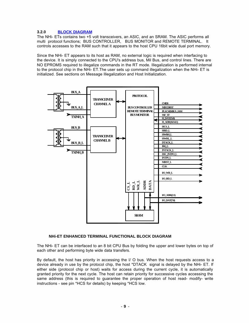
3.2.0 BLOCK DIAGRAMThe NHi- ETs contains two +5 volt transceivers, an ASIC, and an SRAM. The ASIC performs allmulti protocol functions; BUS CONTROLLER, BUS MONITOR and REMOTE TERMINAL. Itcontrols accesses to the RAM such that it appears to the host CPU 16bit wide dual port memory.
Since the NHi- ET appears to its host as RAM, no external logic is required when interfacing tothe device. It is simply connected to the CPU's address bus, Mil Bus, and control lines. There areNO EPROMS required to illegalize commands in the RT mode. Illegalization is performed internalto the protocol chip in the NHi- ET.The user sets up command illegalization when the NHi- ET isinitialized. See sections on Message Illegalization and Host Initialization.
NHi-ET ENHANCED TERMINAL FUNCTIONAL BLOCK DIAGRAM
The NHi- ET can be interfaced to an 8 bit CPU Bus by folding the upper and lower bytes on top ofeach other and performing byte wide data transfers.
By default, the host has priority in accessing the I/ O bus. When the host requests access to adevice already in use by the protocol chip, the host *DTACK signal is delayed by the NHi- ET. Ifeither side (protocol chip or host) waits for access during the current cycle, it is automaticallygranted priority for the next cycle. The host can retain priority for successive cycles accessing thesame address (this is required to guarantee the proper operation of host read- modify- writeinstructions - see pin *HCS for details) by keeping *HCS low.
TRANSCEIVERCHANNEL A
TRANSCEIVERCHANNEL B
PROTOCOL
BUS CONTROLLERREMOTE TERMINAL BUS MONITOR
SRAM
BUS_A
BUS_A_L
TXINH_A
BUS_B
BUS_B_L
TXINH_B
CS_
LR
D_L
WR
_L
AD
DR
DA
TA
CMDSMDCDRSTPLSCMD/BUS_JAMSSF_TFH_DAT(15:0)H_ADR(16/14:1)
HCS_LHRD_LHWRH_LHWRL_LDTACK_LIRQ_LINTACK_LDSC_INTPO_LINTPI_L
MRST_L
CLK
I/O_WR_L
I/O_RD_L
I/O_ADR(2:1)
I/O_DAT(7:0)
- -10
3.3.0 PROTOCOL CHIP DESCRIPTIONThe protocol chip contains the following modules:
Host Bus Interface Unit (HBIU)I/ O Bus Interface Unit (IBIU)Interrupt Controller Unit (ICU)Dual Redundant multi protocol Front End (DRFE)Message Processor Unit (MPU)
3.3.1 HOST BUS INTERFACE UNITThe HBIU provides a standard RAM interface to the host bus. The module performs the followingfunctions:
Provides NHi- ET device select and decodes host address to select registers.Transfers data between the NHi-ET and the host (word and byte mode as well as read- modify- write are supported).Provides priority input and output for daisy chaining host interrupts.Outputs *DTACK signal indicating end of bus cycle.
3.3.2 I/O BUS INTERFACE UNITThe IBIU controls the RAM and I/ O residing on the I/ O bus so that it appears to the host as apseudo dual port RAM (i. e., shared memory). The unit implements the following functions:
Arbitrates between host and protocol chip initiated accesses to the RAM and host data bus.Decodes address lines to select device (e. g. RAM, external byte- wide I/ O, external terminal address buffer, command output register).Generates control signals to access the selected device.
3.3.3 INTERRUPT CONTROL UNITThe ICU is an 8 input vectored interrupt controller. It contains eight registers as well as a FIFO forstoring pending interrupt vectors.
3.3.3.1 ICU REGISTERSThe ICU contains the following registers
INTERRUPT REQUEST register (IRR)INTERRUPT MASK register (IMR)INTERRUPT VECTOR register (IVR)AUXILIARY VECTOR register (AVR)
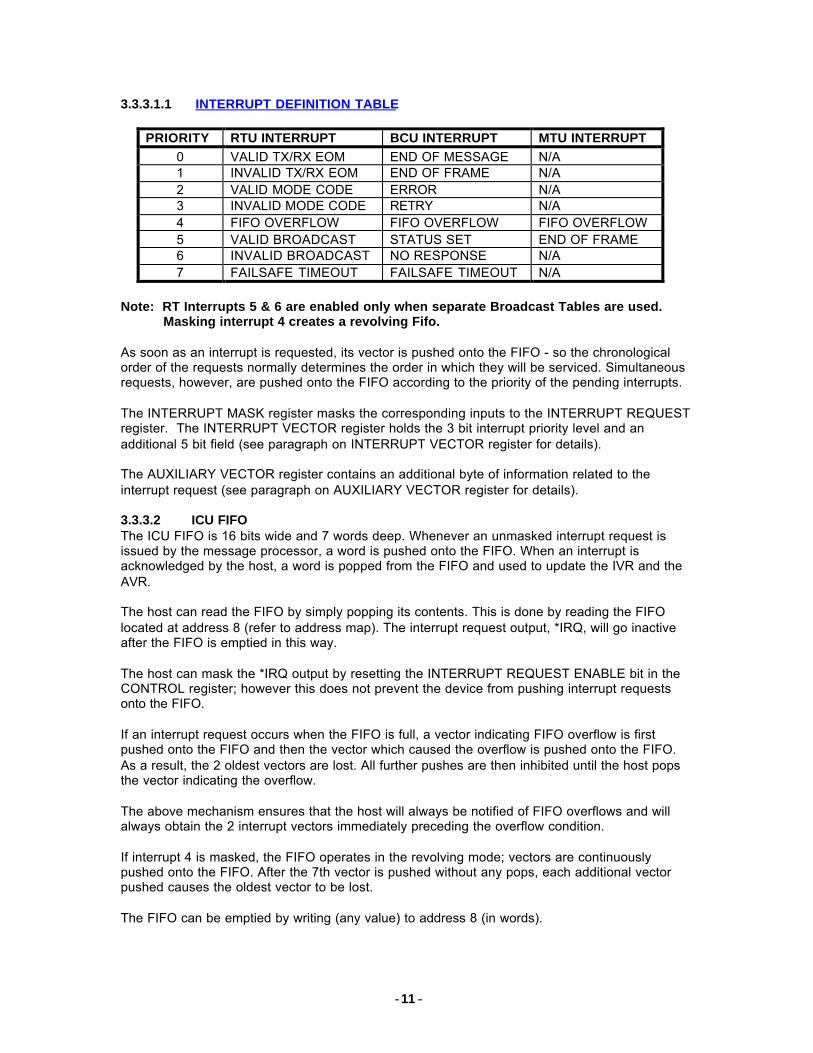
The INTERRUPT REQUEST register samples 8 inputs originating from internal modules. Sincethe host can write to this register, all interrupt sequences can be software driven for programdebugging. The inputs and their priorities (level 7 has highest priority) are described in thefollowing table.
- -11
3.3.3.1.1 INTERRUPT DEFINITION TABLE
PRIORITY RTU INTERRUPT BCU INTERRUPT MTU INTERRUPT0 VALID TX/RX EOM END OF MESSAGE N/A1 INVALID TX/RX EOM END OF FRAME N/A2 VALID MODE CODE ERROR N/A3 INVALID MODE CODE RETRY N/A4 FIFO OVERFLOW FIFO OVERFLOW FIFO OVERFLOW5 VALID BROADCAST STATUS SET END OF FRAME6 INVALID BROADCAST NO RESPONSE N/A7 FAILSAFE TIMEOUT FAILSAFE TIMEOUT N/A
Note: RT Interrupts 5 & 6 are enabled only when separate Broadcast Tables are used. Masking interrupt 4 creates a revolving Fifo.
As soon as an interrupt is requested, its vector is pushed onto the FIFO - so the chronologicalorder of the requests normally determines the order in which they will be serviced. Simultaneousrequests, however, are pushed onto the FIFO according to the priority of the pending interrupts.
The INTERRUPT MASK register masks the corresponding inputs to the INTERRUPT REQUESTregister. The INTERRUPT VECTOR register holds the 3 bit interrupt priority level and anadditional 5 bit field (see paragraph on INTERRUPT VECTOR register for details).
The AUXILIARY VECTOR register contains an additional byte of information related to theinterrupt request (see paragraph on AUXILIARY VECTOR register for details).
3.3.3.2 ICU FIFOThe ICU FIFO is 16 bits wide and 7 words deep. Whenever an unmasked interrupt request isissued by the message processor, a word is pushed onto the FIFO. When an interrupt isacknowledged by the host, a word is popped from the FIFO and used to update the IVR and theAVR.
The host can read the FIFO by simply popping its contents. This is done by reading the FIFOlocated at address 8 (refer to address map). The interrupt request output, *IRQ, will go inactiveafter the FIFO is emptied in this way.
The host can mask the *IRQ output by resetting the INTERRUPT REQUEST ENABLE bit in theCONTROL register; however this does not prevent the device from pushing interrupt requestsonto the FIFO.
If an interrupt request occurs when the FIFO is full, a vector indicating FIFO overflow is firstpushed onto the FIFO and then the vector which caused the overflow is pushed onto the FIFO.As a result, the 2 oldest vectors are lost. All further pushes are then inhibited until the host popsthe vector indicating the overflow.
The above mechanism ensures that the host will always be notified of FIFO overflows and willalways obtain the 2 interrupt vectors immediately preceding the overflow condition.
If interrupt 4 is masked, the FIFO operates in the revolving mode; vectors are continuouslypushed onto the FIFO. After the 7th vector is pushed without any pops, each additional vectorpushed causes the oldest vector to be lost.
The FIFO can be emptied by writing (any value) to address 8 (in words).
- -12
3.3.4 DUAL REDUNDANT FRONT ENDThe DRFE performs serial to parallel and parallel to serial conversion as well as basic format andtiming validation. The unit contains the following:
Manchester encoders/ decodersGap counterNo response counterMinimum response time counterTimeout counter
3.3.4.1 MANCHESTER DECODERThe decoder translates serial Manchester bi- phase signals to 16- bit words and outputs thefollowing signals:
Valid command word receivedValid data word receivedInvalid word received (parity, incorrect bit count, invalid Manchester encoding, gap)Broadcast command receivedBegin new message (i. e., end of a valid legal command for this Remote Terminal)
3.3.4.2 MANCHESTER ENCODERThe encoder receives 16 bit words and transmits them with the appropriate sync and parity as aserial Manchester bi- phase signal. The outputs of the encoder can be loop- backed into eitherdecoder for test purposes.
3.3.4.3 GAP COUNTERThe gap counter checks contiguity of successive words. If the time between "contiguous" words(measured from zero- cross of parity to zero- cross of sync) exceeds 3.5 - 3.7 microseconds, themessage is invalidated.
3.3.4.4 RT - RT NO RESPONSE COUNTERThe no response counter checks the response time of the transmitting RT in a RT to RT transfer.If the response time is exceeded, the message is invalidated. The response time is softwareprogrammable (14, 18, 26, 42 microseconds) to accommodate systems with long cables and/ orslow terminals.
3.3.4.5 MINIMUM RESPONSE TIME COUNTERThe minimum response time counter ensures that the response will be no sooner than 4microseconds(measured from zero- cross of parity to zero- cross of sync).
3.3.4.6 FAIL -SAFE TIMEOUT COUNTERThis counter inhibits the encoder outputs and issues a TIMEOUT interrupt whenever continuoustransmission exceeds 768/ 672 microseconds. Transmission will remain inhibited until acommand is received on the same bus or the part is reset.
3.3.5 MESSAGE PROCESSOR UNITThe MPU forms the heart of the protocol chip and controls the operation of the Decoders,Encoders, and Interrupt Controller. This unit is activated by the reception of a valid legalcommand addressed to the RT in the RT mode and the START bit in CONFIGURATION 1 in boththe BC and MT modes.
- -13
The MPU performs the following functions:
Recognizes the various message types (for BC, MT, and RT) and responds with the appropriate sequence of control signals. Validates format and timing of received data words. Checks command legality. Responds with status/ data. Calculates all addresses for accessing the RAM and discrete I/ O. Updates RAM data table contents, including tag words. Optionally time tags data tables. Issues interrupt requests to the ICU. The maximum response time of the NHi- ET in the RT mode is less than 6.0 microseconds (measured from zero- cross to zero- cross).
3.4.0 RT HARDWIRE TERMINAL ADDRESS
The terminal address of the NHi- ET can be hardwired using I/ O DAT( 5: 0). I/ O DAT( 4: 0) areused for the terminal address, I/ O DAT0 being the LSB, and I/ O DAT5 is used to set odd parityin the address. These pins CANNOT be directly connected to +5 or ground since the I/ O databus drives the NHi- ET's internal RAM.
The address must be wired using pull- up and pull- down resistors. There are 64K internal pull- upresistors in the protocol chip, so only external pull- down resistors of 4.7K are required. TheHardwire Address is read and loaded into the terminal at Power- On Reset, Hardware Reset, andSoftware Reset.
The terminal address can be changed at any time through software by writing a new address tothe Basic Status Register, however, if any of the above resets occur, the Hardwire Address willbe re- loaded into the terminal. The software address can be locked out by setting Bit2 inConfiguration Register 1.
4.0.0 DATA STRUCTURE
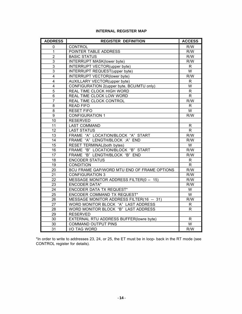
4.1.0 ADDRESS MAPThe NHi- ET appears to the host as 16K or 64K words of memory divided into the followingblocks:
ADDRESS RANGE DESCRIPTION0 -- 30 INTERNAL REGISTERS31 I/O TAG WORD32 -- 35 I/O SPACE64 -- 16383/65535 SHARED RAM
- -14
INTERNAL REGISTER MAP
ADDRESS REGISTER DEFINITION ACCESS0 CONTROL R/W1 POINTER TABLE ADDRESS R/W2 BASIC STATUS R/W3 INTERRUPT MASK(lower byte) R/W3 INTERRUPT VECTOR(upper byte) R3 INTERRUPT REQUEST(upper byte) W4 INTERRUPT VECTOR(lower byte) R/W4 AUXILLARY VECTOR(upper byte) R4 CONFIGURATION 2(upper byte, BCU/MTU only) W5 REAL TIME CLOCK HIGH WORD R6 REAL TIME CLOCK LOW WORD R7 REAL TIME CLOCK CONTROL R/W8 READ FIFO R8 RESET FIFO W9 CONFIGURATION 1 R/W10 RESERVED11 LAST COMMAND R12 LAST STATUS R13 FRAME “A” LOCATION/BLOCK “A” START R/W14 FRAME “A” LENGTH/BLOCK :A” END R/W15 RESET TERMINAL(both bytes) W16 FRAME “B” LOCATION/BLOCK “B” START R/W17 FRAME “B” LENGTH/BLOCK “B” END R/W18 ENCODER STATUS R19 CONDITION R20 BCU FRAME GAP/WORD MTU END OF FRAME OPTIONS R/W21 CONFIGURATION 3 R/W22 MESSAGE MONITOR ADDRESS FILTER(0 -- 15) R/W23 ENCODER DATA* R/W24 ENCODER DATA TX REQUEST* W25 ENCODER COMMAND TX REQUEST* W26 MESSAGE MONITOR ADDRESS FILTER(16 -- 31) R/W27 WORD MONITOR BLOCK “A” LAST ADDRESS R28 WORD MONITOR BLOCK “B” LAST ADDRESS R29 RESERVED30 EXTERNAL RTU ADDRESS BUFFER(lowre byte) R30 COMMAND OUTPUT PINS W31 I/O TAG WORD R/W
*In order to write to addresses 23, 24, or 25, the ET must be in loop- back in the RT mode (seeCONTROL register for details).
- -15
4.2.0 INTERNAL REGISTERS
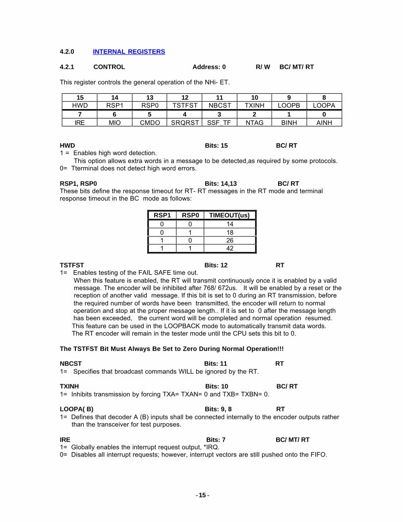
4.2.1 CONTROL Address: 0 R/ W BC/ MT/ RT
This register controls the general operation of the NHi- ET.
15 14 13 12 11 10 9 8HWD RSP1 RSP0 TSTFST NBCST TXINH LOOPB LOOPA
7 6 5 4 3 2 1 0IRE MIO CMDO SRQRST SSF_TF NTAG BINH AINH
HWD Bits: 15 BC/ RT1 = Enables high word detection. This option allows extra words in a message to be detected,as required by some protocols.0= Tterminal does not detect high word errors.
RSP1, RSP0 Bits: 14,13 BC/ RTThese bits define the response timeout for RT- RT messages in the RT mode and terminalresponse timeout in the BC mode as follows:
RSP1 RSP0 TIMEOUT(us)0 0 140 1 181 0 261 1 42
TSTFST Bits: 12 RT1= Enables testing of the FAIL SAFE time out. When this feature is enabled, the RT will transmit continuously once it is enabled by a valid message. The encoder will be inhibited after 768/ 672us. It will be enabled by a reset or the reception of another valid message. If this bit is set to 0 during an RT transmission, before the required number of words have been transmitted, the encoder will return to normal operation and stop at the proper message length.. If it is set to 0 after the message length has been exceeded, the current word will be completed and normal operation resumed. This feature can be used in the LOOPBACK mode to automatically transmit data words. The RT encoder will remain in the tester mode until the CPU sets this bit to 0.
The TSTFST Bit Must Always Be Set to Zero During Normal Operation!!!
NBCST Bits: 11 RT1= Specifies that broadcast commands WILL be ignored by the RT.
TXINH Bits: 10 BC/ RT1= Inhibits transmission by forcing TXA= TXAN= 0 and TXB= TXBN= 0.
LOOPA( B) Bits: 9, 8 RT1= Defines that decoder A (B) inputs shall be connected internally to the encoder outputs rather than the transceiver for test purposes.
IRE Bits: 7 BC/ MT/ RT1= Globally enables the interrupt request output, *IRQ.0= Disables all interrupt requests; however, interrupt vectors are still pushed onto the FIFO.
- -16
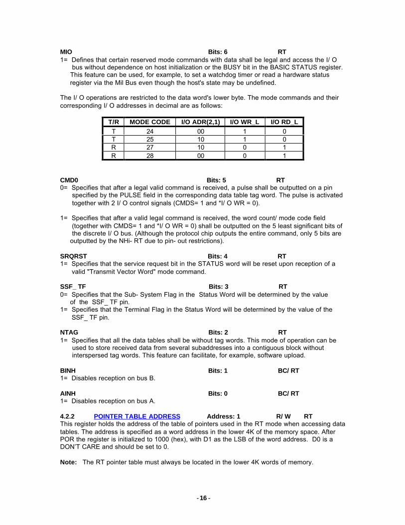
MIO Bits: 6 RT1= Defines that certain reserved mode commands with data shall be legal and access the I/ O bus without dependence on host initialization or the BUSY bit in the BASIC STATUS register. This feature can be used, for example, to set a watchdog timer or read a hardware status register via the Mil Bus even though the host's state may be undefined.
The I/ O operations are restricted to the data word's lower byte. The mode commands and theircorresponding I/ O addresses in decimal are as follows:
T/R MODE CODE I/O ADR(2,1) I/O WR_L I/O RD_LT 24 00 1 0T 25 10 1 0R 27 10 0 1R 28 00 0 1
CMD0 Bits: 5 RT0= Specifies that after a legal valid command is received, a pulse shall be outputted on a pin specified by the PULSE field in the corresponding data table tag word. The pulse is activated together with 2 I/ O control signals (CMDS= 1 and *I/ O WR = 0).
1= Specifies that after a valid legal command is received, the word count/ mode code field (together with CMDS= 1 and *I/ O WR = 0) shall be outputted on the 5 least significant bits of the discrete I/ O bus. (Although the protocol chip outputs the entire command, only 5 bits are outputted by the NHi- RT due to pin- out restrictions).
SRQRST Bits: 4 RT1= Specifies that the service request bit in the STATUS word will be reset upon reception of a valid "Transmit Vector Word" mode command.
SSF_ TF Bits: 3 RT0= Specifies that the Sub- System Flag in the Status Word will be determined by the value of the SSF_ TF pin.1= Specifies that the Terminal Flag in the Status Word will be determined by the value of the SSF_ TF pin.
NTAG Bits: 2 RT1= Specifies that all the data tables shall be without tag words. This mode of operation can be used to store received data from several subaddresses into a contiguous block without interspersed tag words. This feature can facilitate, for example, software upload.
BINH Bits: 1 BC/ RT1= Disables reception on bus B.
AINH Bits: 0 BC/ RT1= Disables reception on bus A.
4.2.2 POINTER TABLE ADDRESS Address: 1 R/ W RTThis register holds the address of the table of pointers used in the RT mode when accessing datatables. The address is specified as a word address in the lower 4K of the memory space. AfterPOR the register is initialized to 1000 (hex), with D1 as the LSB of the word address. D0 is aDON’T CARE and should be set to 0.
Note: The RT pointer table must always be located in the lower 4K words of memory.
- -17
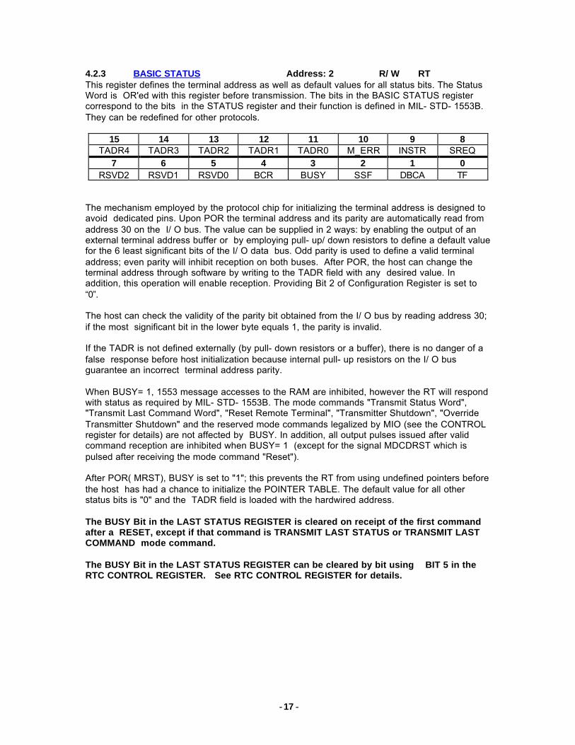
4.2.3 BASIC STATUS Address: 2 R/ W RTThis register defines the terminal address as well as default values for all status bits. The StatusWord is OR'ed with this register before transmission. The bits in the BASIC STATUS registercorrespond to the bits in the STATUS register and their function is defined in MIL- STD- 1553B.They can be redefined for other protocols.
15 14 13 12 11 10 9 8TADR4 TADR3 TADR2 TADR1 TADR0 M_ERR INSTR SREQ
7 6 5 4 3 2 1 0RSVD2 RSVD1 RSVD0 BCR BUSY SSF DBCA TF
The mechanism employed by the protocol chip for initializing the terminal address is designed toavoid dedicated pins. Upon POR the terminal address and its parity are automatically read fromaddress 30 on the I/ O bus. The value can be supplied in 2 ways: by enabling the output of anexternal terminal address buffer or by employing pull- up/ down resistors to define a default valuefor the 6 least significant bits of the I/ O data bus. Odd parity is used to define a valid terminaladdress; even parity will inhibit reception on both buses. After POR, the host can change theterminal address through software by writing to the TADR field with any desired value. Inaddition, this operation will enable reception. Providing Bit 2 of Configuration Register is set to“0”.
The host can check the validity of the parity bit obtained from the I/ O bus by reading address 30;if the most significant bit in the lower byte equals 1, the parity is invalid.
If the TADR is not defined externally (by pull- down resistors or a buffer), there is no danger of afalse response before host initialization because internal pull- up resistors on the I/ O busguarantee an incorrect terminal address parity.
When BUSY= 1, 1553 message accesses to the RAM are inhibited, however the RT will respondwith status as required by MIL- STD- 1553B. The mode commands "Transmit Status Word","Transmit Last Command Word", "Reset Remote Terminal", "Transmitter Shutdown", "OverrideTransmitter Shutdown" and the reserved mode commands legalized by MIO (see the CONTROLregister for details) are not affected by BUSY. In addition, all output pulses issued after validcommand reception are inhibited when BUSY= 1 (except for the signal MDCDRST which ispulsed after receiving the mode command "Reset").
After POR( MRST), BUSY is set to "1"; this prevents the RT from using undefined pointers beforethe host has had a chance to initialize the POINTER TABLE. The default value for all otherstatus bits is "0" and the TADR field is loaded with the hardwired address.
The BUSY Bit in the LAST STATUS REGISTER is cleared on receipt of the first commandafter a RESET, except if that command is TRANSMIT LAST STATUS or TRANSMIT LASTCOMMAND mode command.
The BUSY Bit in the LAST STATUS REGISTER can be cleared by bit using BIT 5 in theRTC CONTROL REGISTER. See RTC CONTROL REGISTER for details.
- -18
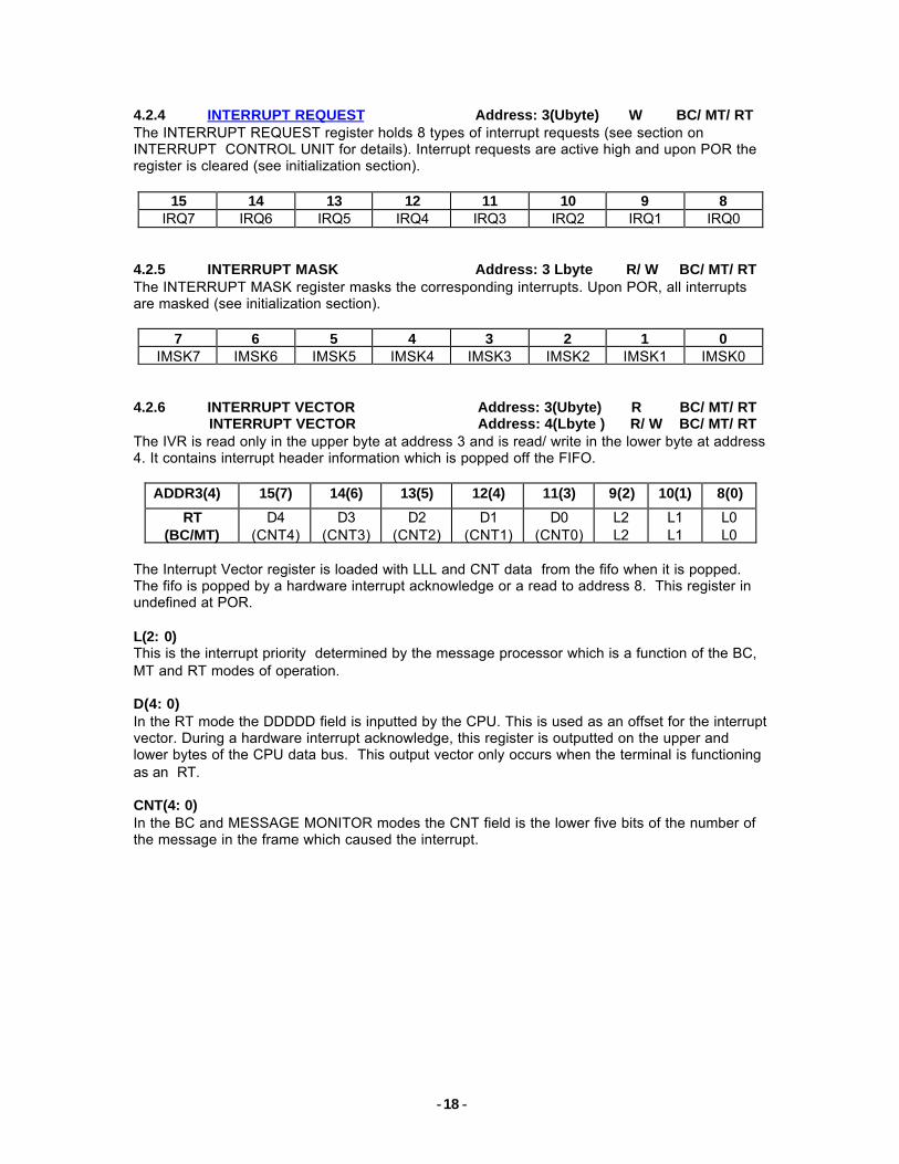
4.2.4 INTERRUPT REQUEST Address: 3(Ubyte) W BC/ MT/ RTThe INTERRUPT REQUEST register holds 8 types of interrupt requests (see section onINTERRUPT CONTROL UNIT for details). Interrupt requests are active high and upon POR theregister is cleared (see initialization section).
15 14 13 12 11 10 9 8IRQ7 IRQ6 IRQ5 IRQ4 IRQ3 IRQ2 IRQ1 IRQ0
4.2.5 INTERRUPT MASK Address: 3 Lbyte R/ W BC/ MT/ RTThe INTERRUPT MASK register masks the corresponding interrupts. Upon POR, all interruptsare masked (see initialization section).
7 6 5 4 3 2 1 0IMSK7 IMSK6 IMSK5 IMSK4 IMSK3 IMSK2 IMSK1 IMSK0
4.2.6 INTERRUPT VECTOR Address: 3(Ubyte) R BC/ MT/ RT INTERRUPT VECTOR Address: 4(Lbyte ) R/ W BC/ MT/ RTThe IVR is read only in the upper byte at address 3 and is read/ write in the lower byte at address4. It contains interrupt header information which is popped off the FIFO.
ADDR3(4) 15(7) 14(6) 13(5) 12(4) 11(3) 9(2) 10(1) 8(0)
RT(BC/MT)
D4(CNT4)
D3(CNT3)
D2(CNT2)
D1(CNT1)
D0(CNT0)
L2L2
L1L1
L0L0
The Interrupt Vector register is loaded with LLL and CNT data from the fifo when it is popped.The fifo is popped by a hardware interrupt acknowledge or a read to address 8. This register inundefined at POR.
L(2: 0)This is the interrupt priority determined by the message processor which is a function of the BC,MT and RT modes of operation.
D(4: 0)In the RT mode the DDDDD field is inputted by the CPU. This is used as an offset for the interruptvector. During a hardware interrupt acknowledge, this register is outputted on the upper andlower bytes of the CPU data bus. This output vector only occurs when the terminal is functioningas an RT.
CNT(4: 0)In the BC and MESSAGE MONITOR modes the CNT field is the lower five bits of the number ofthe message in the frame which caused the interrupt.
- -19
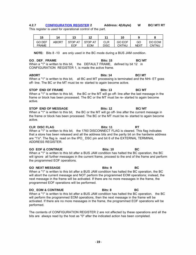
4.2.7 CONFIGURATION REGISTER 2 Address: 4(Ubyte) W BC/ MT/ RTThis register is used for operational control of the part.
15 14 13 12 11 10 9 8GO DEFFRAME
ABORT STOP ATEOF
STOP ATEOM
CLRDISC
GO EOFCNTNU
GONEXT
DO EOMCNTNU
NOTE: Bits 8 -10 are only used in the BC mode during a BUS JAM condition.
GO_ DEF_ FRAME Bits: 15 BC/ MTWhen a "1" is written to this bit, the DEFAULT FRAME, defined by bit 12 inCONFIGURATION REGISTER 1, is made the active frame.
ABORT Bits: 14 BC/ MTWhen a "1" is written to this bit, all BC and MT processing is terminated and the NHi- ET goesoff- line. The BC or the MT must be re- started to again become active.
STOP END OF FRAME Bits: 13 BC/ MTWhen a "1" is written to this bit, the BC or the MT will go off- line after the last message in theframe or block has been processed. The BC or the MT must be re- started to again becomeactive.
STOP END OF MESSAGE Bits: 12 BC/ MTWhen a "1" is written to this bit, the BC or the MT will go off- line after the current message inthe frame or block has been processed. The BC or the MT must be re- started to again becomeactive.
CLR DISC FLAG Bits: 11 RTWhen a "1" is written to this bit, the 1760 DISCONNECT FLAG is cleared. This flag indicatesthat a store has been released and all the address bits and the parity bit on the hardwire addressare "1's". The flag is read on the IPO_ DSC pin and bit 6 of the EXTERNAL TERMINALADDRESS REGISTER.
GO EOF & CONTINUE Bits: 10 BCWhen a "1" is written to this bit after a BUS JAM condition has halted the BC operation, the BCwill ignore all further messages in the current frame, proceed to the end of the frame and performthe programmed EOF operations.
GO NEXT MESSAGE Bits: 9 BCWhen a "1" is written to this bit after a BUS JAM condition has halted the BC operation, the BCwill abort the current message and NOT perform the programmed EOM operations; instead, thenext message in the frame will be activated. If there are no more messages in the frame, theprogrammed EOF operations will be performed.
DO_ EOM & CONTINUE Bits: 8 BCWhen a "1" is written to this bit after a BUS JAM condition has halted the BC operation, the BCwill perform the programmed EOM operations, then the next message in the frame will beactivated. If there are no more messages in the frame, the programmed EOF operations will beperformed.
The contents of CONFIGURATION REGISTER 2 are not affected by these operations and all thebits are always read by the host as "0" after the indicated action has been completed.
- -20
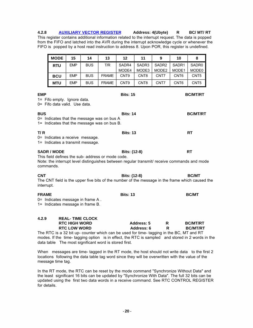
4.2.8 AUXILIARY VECTOR REGISTER Address: 4(Ubyte) R BC/ MT/ RTThis register contains additional information related to the interrupt request. The data is poppedfrom the FIFO and latched into the AVR during the interrupt acknowledge cycle or whenever theFIFO is popped by a host read instruction to address 8. Upon POR, this register is undefined.
MODE 15 14 13 12 11 9 10 8
RTU EMP BUS T/R SADR4MODE4
SADR3MODE3
SADR2MODE2
SADR1MODE1
SADR0MODE0
BCU EMP BUS FRAME CNT9 CNT8 CNT7 CNT6 CNT5
MTU EMP BUS FRAME CNT9 CNT8 CNT7 CNT6 CNT5
EMP Bits: 15 BC/MT/RT1= Fifo empty. Ignore data.0= Fifo data valid. Use data.
BUS Bits: 14 BC/MT/RT0= Indicates that the message was on bus A1= Indicates that the message was on bus B.
T/ R Bits: 13 RT0= Indicates a receive message.1= Indicates a transmit message.
SADR / MODE Bits: (12-8) RTThis field defines the sub- address or mode code.Note: the interrupt level distinguishes between regular transmit/ receive commands and modecommands.
CNT Bits: (12-8) BC/MTThe CNT field is the upper five bits of the number of the message in the frame which caused theinterrupt.
FRAME Bits: 13 BC/MT0= Indicates message in frame A .1= Indicates message in frame B.
4.2.9 REAL- TIME CLOCK RTC HIGH WORD Address: 5 R BC/MT/RT RTC LOW WORD Address: 6 R BC/MT/RTThe RTC is a 32 bit up- counter which can be used for time- tagging in the BC, MT and RTmodes. If the time- tagging option is in effect, the RTC is sampled and stored in 2 words in thedata table The most significant word is stored first.
When messages are time- tagged in the RT mode, the host should not write data to the first 2locations following the data table tag word since they will be overwritten with the value of themessage time tag.
In the RT mode, the RTC can be reset by the mode command "Synchronize Without Data" andthe least significant 16 bits can be updated by "Synchronize With Data". The full 32 bits can beupdated using the first two data words in a receive command. See RTC CONTROL REGISTERfor details.
- -21
The RTC can be read and reset by the host at any time. Since the RTC consists of 32 bits, atleast 2 memory cycles are required to read all of its value. As a result, a carry- out from the lowerword can occur between the read cycles. A mechanism is therefore provided to solve thispotential difficulty.
If the host reads the RTC as two 16 bit words, *LOCK should be initialized to 1 in the RTCCONTROL register. In this case, when the host reads the upper word, all 32 bits are latched intothe host output register. The value in the output register remains unchanged until the hostfinishes reading the lower word of the RTC.
If the host reads the RTC in bytes, *LOCK should be initialized to 0. In this case, when the hostreads any of the bytes of the RTC, all 32 bits are latched into the host output register and itsvalue remains unchanged until updating is re- enabled by reading the RTC CONTROL register.The RTC resolution can be programmed equal to 1, 2, 4, 8, 16, 32, or 64 microseconds.
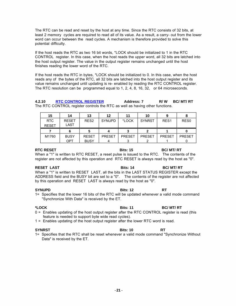
4.2.10 RTC CONTROL REGISTER Address: 7 R/ W BC/ MT/ RTThe RTC CONTROL register controls the RTC as well as having other functions.
15 14 13 12 11 10 9 8RTC
RESETRESETLAST
RES2 SYNUPD *LOCK SYNRST RES1 RES0
7 6 5 4 3 2 1 0M1760 BUSY
OPTRESETBUSY
PRESET4
PRESET3
PRESET2
PRESET1
PRESET0
RTC RESET Bits: 15 BC/ MT/ RTWhen a "1" is written to RTC RESET, a reset pulse is issued to the RTC. The contents of theregister are not affected by this operation and RTC RESET is always read by the host as "0".
RESET LAST Bits: 14 BC/ MT/ RTWhen a "1" is written to RESET LAST, all the bits in the LAST STATUS REGISTER except theADDRESS field and the BUSY bit are set to a "0". The contents of the register are not affectedby this operation and RESET LAST is always read by the host as "0".
SYNUPD Bits: 12 RT1= Specifies that the lower 16 bits of the RTC will be updated whenever a valid mode command "Synchronize With Data" is received by the ET.
*LOCK Bits: 11 BC/ MT/ RT0 = Enables updating of the host output register after the RTC CONTROL register is read (this feature is needed to support byte wide read cycles).1 = Enables updating of the host output register after the lower RTC word is read.
SYNRST Bits: 10 RT1= Specifies that the RTC shall be reset whenever a valid mode command "Synchronize Without Data" is received by the ET.
- -22
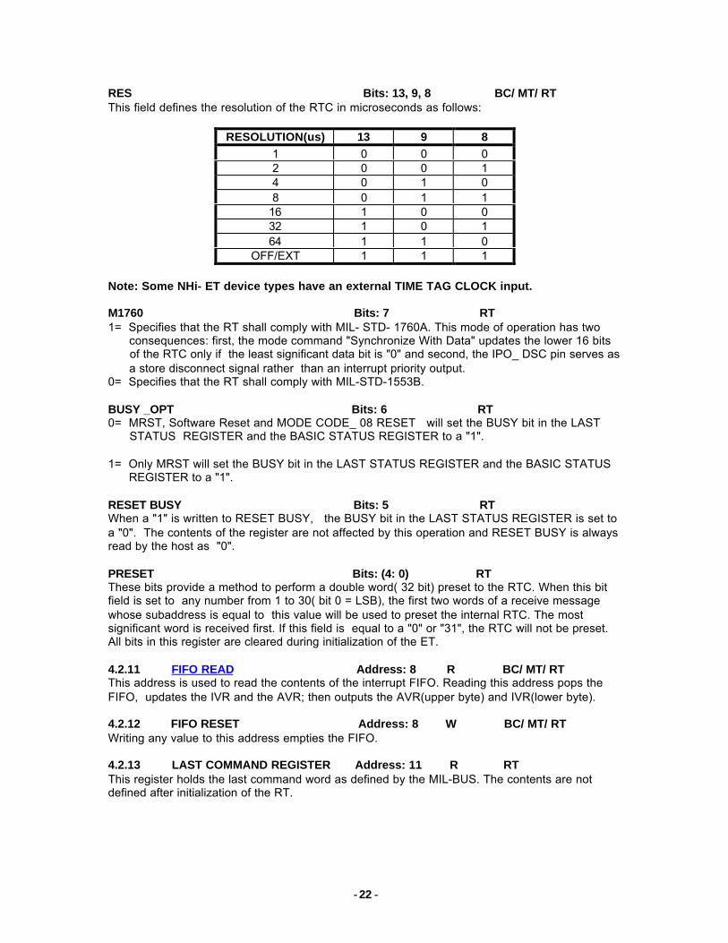
RES Bits: 13, 9, 8 BC/ MT/ RTThis field defines the resolution of the RTC in microseconds as follows:
RESOLUTION(us) 13 9 81 0 0 02 0 0 14 0 1 08 0 1 1
16 1 0 032 1 0 164 1 1 0
OFF/EXT 1 1 1
Note: Some NHi- ET device types have an external TIME TAG CLOCK input.
M1760 Bits: 7 RT1= Specifies that the RT shall comply with MIL- STD- 1760A. This mode of operation has two consequences: first, the mode command "Synchronize With Data" updates the lower 16 bits of the RTC only if the least significant data bit is "0" and second, the IPO_ DSC pin serves as a store disconnect signal rather than an interrupt priority output.0= Specifies that the RT shall comply with MIL-STD-1553B.
BUSY _OPT Bits: 6 RT0= MRST, Software Reset and MODE CODE_ 08 RESET will set the BUSY bit in the LAST STATUS REGISTER and the BASIC STATUS REGISTER to a "1".
1= Only MRST will set the BUSY bit in the LAST STATUS REGISTER and the BASIC STATUS REGISTER to a "1".
RESET BUSY Bits: 5 RTWhen a "1" is written to RESET BUSY, the BUSY bit in the LAST STATUS REGISTER is set toa "0". The contents of the register are not affected by this operation and RESET BUSY is alwaysread by the host as "0".
PRESET Bits: (4: 0) RTThese bits provide a method to perform a double word( 32 bit) preset to the RTC. When this bitfield is set to any number from 1 to 30( bit 0 = LSB), the first two words of a receive messagewhose subaddress is equal to this value will be used to preset the internal RTC. The mostsignificant word is received first. If this field is equal to a "0" or "31", the RTC will not be preset.All bits in this register are cleared during initialization of the ET.
4.2.11 FIFO READ Address: 8 R BC/ MT/ RTThis address is used to read the contents of the interrupt FIFO. Reading this address pops theFIFO, updates the IVR and the AVR; then outputs the AVR(upper byte) and IVR(lower byte).
4.2.12 FIFO RESET Address: 8 W BC/ MT/ RTWriting any value to this address empties the FIFO.
4.2.13 LAST COMMAND REGISTER Address: 11 R RTThis register holds the last command word as defined by the MIL-BUS. The contents are notdefined after initialization of the RT.
- -23
4.2.14 LAST STATUS REGISTER Address: 12 R RTThis register holds the Status Word assosciated with the last message. After initialization of theRT, the BUSY bit= 1, the TADR field contains the hardwire address, and all other bits are set to0. See RTC CONTROL REGISTER for special options.
4.2.15 RESET REMOTE TERMINAL Address: 15 W BC/ MT/ RTWriting a word to address 15 resets the RT and causes it to perform its initialization (seeinitialization section).
4.2.16 ENCODER STATUS Address: 18 R BC/ RTThis register contains flags indicating the status of the encoder. These flags are intended tofacilitate transmission of messages in loop- back mode during self- test.
15 7 0TXREQ_L EOTX_L FAILSAFE_L
TXREQ_ L Bits: 15 RT0= Indicates that the encoder is ready to accept the next word for transmission. This bit should equal "0" before loading the Encoder Data register with the next word. In order to transmit contiguous words, the next word should be loaded within 18 microseconds after *TXREQ transitions to "0".
EOTX_ L Bits: 7 RT0= Indicates that the encoder has completed transmission and that there are no pending requests.
FAILSAFE_ L Bits: 0 BC/ RT0= FAILSAFE TIME OUT has occurred. This bit will be set to a "1" when a new message is received or during a reset.
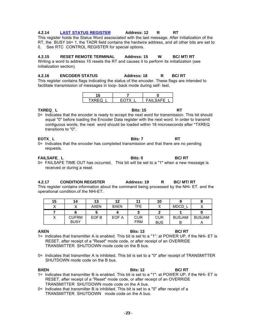
4.2.17 CONDITION REGISTER Address: 19 R BC/ MT/ RTThis register contains information about the command being processed by the NHi- ET. and theoperational condition.of the NHi-ET.
15 14 13 12 11 10 9 8X X AXEN BXEN TFE X MDCD_L X7 6 5 4 3 2 1 0X CUFRM
BUSYEOF B EOF A CUR
FRMCURBUS
BUSJAMB
BUSJAMA
AXEN Bits: 13 BC/ RT1= Indicates that transmitter A is enabled. This bit is set to a "1": at POWER UP, if the NHi- ET is RESET, after receipt of a "Reset" mode code, or after receipt of an OVERRIDE TRANSMITTER SHUTDOWN mode code on the B bus.
0= Indicates that transmitter A is inhibited. This bit is set to a "0" after receipt of TRANSMITTER SHUTDOWN mode code on the B bus.
BXEN Bits: 12 BC/ RT1= Indicates that transmitter B is enabled. This bit is set to a "1": at POWER UP, if the NHi- ET is RESET, after receipt of a "Reset" mode code, or after receipt of an OVERRIDE TRANSMITTER SHUTDOWN mode code on the A bus.0= Indicates that transmitter B is inhibited. This bit is set to a "0" after receipt of a TRANSMITTER SHUTDOWN mode code on the A bus.
- -24
TFE Bits: 11 RT1= Indicates that the TERMINAL FLAG bit in the status word can be set to a "1" . This can be done in the BASIC STATUS REGISTER or by the TERMINAL FLAG pin on the NHi-ET. This bit is set to a "1" at POWER UP, if the NHi- ET is RESET, after receipt of a RESET MODE CODE, or after receipt of an OVERRIDE INHIBIT TERMINAL FLAG mode code.0= Indicates that the TERMINAL FLAG bit in the status word CANNOT be set to a "1". This bit is set to a "0" after receipt of an INHIBIT TERMINAL FLAG mode code.
MDCD_ L Bits: 9 RT1= Indicates that the last command received was NOT a mode code.0= This bit is set to a "0" when a mode code is received.
CUFRM BUSY Bits: 6 BC/ MT1= The current frame of data block is busy. It is active and could be receiving or transmitting data.
EOF B Bits: 5 BC/ MT1= Frame "B" or data block "B" has finished processing data and in now inactive.
EOF A Bits: 4 BC/ MT1= Frame "A" or data block "A" has finished processing data and in now inactive.
CUR FRM Bits: 3 BC/ MT0= Frame "A" or block "A" is the current active frame of block.1= Frame "B" or block "B" is the current active frame of block.
CUR_ BUS Bits: 2 BC/ MT0= Bus "A" is the current bus.1= Bus "B". is the current bus.
BUSJAM B Bits: 1 BC1 = Bus "B" has been jammed by continuous transmission from an RT. This condition is indicated when an RT transmits more extra words then the value set in CONFIGURATION REGISTER 3 (See CONFIG REG 3 for details).
BUSJAM A Bits: 0 BC1 = Bus "A" has been jammed by continuous transmission from an RT. This condition is indicated when an RT transmits more extra words then the value set in CONFIGURATION REGISTER 3 (See CONFIG REG 3 for details).
4.2.18 ENCODER DATA REGISTER Address: 23 R/W RTThis register contains data to be transmitted when performing a loop back test.
4.2.19 ENCODER DATA TRANSMIT RQST Address: 24 W RTWriting (any value) to this address causes the contents of the ENCODER DATA REGISTER to besent as a data word. This instruction together with the ENCODER COMMAND TRANSMITREQUEST can be used to loop- back entire messages for self- test purposes. The received datacan be read from the data table associated with the command.
4.2.20 ENCODER COMMAND TRANSMIT REQUEST Address: 25 W RTWriting (any value) to this address causes the contents of the ENCODER DATA REGISTER to besent as a command word. This instruction is useful for sending commands to the decoder whilein loop- back mode. The command can then be read from the LAST COMMAND register.
- -25
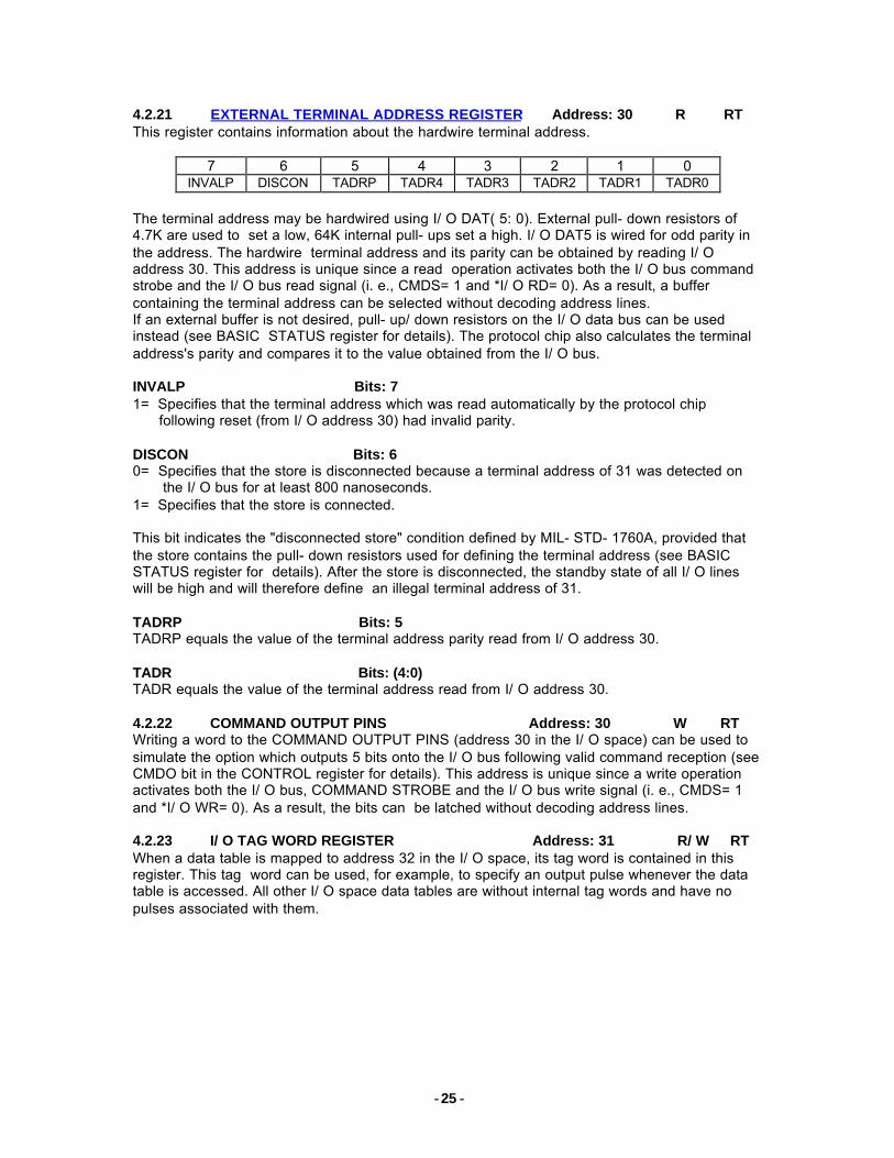
4.2.21 EXTERNAL TERMINAL ADDRESS REGISTER Address: 30 R RTThis register contains information about the hardwire terminal address.
7 6 5 4 3 2 1 0INVALP DISCON TADRP TADR4 TADR3 TADR2 TADR1 TADR0
The terminal address may be hardwired using I/ O DAT( 5: 0). External pull- down resistors of4.7K are used to set a low, 64K internal pull- ups set a high. I/ O DAT5 is wired for odd parity inthe address. The hardwire terminal address and its parity can be obtained by reading I/ Oaddress 30. This address is unique since a read operation activates both the I/ O bus commandstrobe and the I/ O bus read signal (i. e., CMDS= 1 and *I/ O RD= 0). As a result, a buffercontaining the terminal address can be selected without decoding address lines.If an external buffer is not desired, pull- up/ down resistors on the I/ O data bus can be usedinstead (see BASIC STATUS register for details). The protocol chip also calculates the terminaladdress's parity and compares it to the value obtained from the I/ O bus.
INVALP Bits: 71= Specifies that the terminal address which was read automatically by the protocol chip following reset (from I/ O address 30) had invalid parity.
DISCON Bits: 60= Specifies that the store is disconnected because a terminal address of 31 was detected on the I/ O bus for at least 800 nanoseconds.1= Specifies that the store is connected.
This bit indicates the "disconnected store" condition defined by MIL- STD- 1760A, provided thatthe store contains the pull- down resistors used for defining the terminal address (see BASICSTATUS register for details). After the store is disconnected, the standby state of all I/ O lineswill be high and will therefore define an illegal terminal address of 31.
TADRP Bits: 5TADRP equals the value of the terminal address parity read from I/ O address 30.
TADR Bits: (4:0)TADR equals the value of the terminal address read from I/ O address 30.
4.2.22 COMMAND OUTPUT PINS Address: 30 W RTWriting a word to the COMMAND OUTPUT PINS (address 30 in the I/ O space) can be used tosimulate the option which outputs 5 bits onto the I/ O bus following valid command reception (seeCMDO bit in the CONTROL register for details). This address is unique since a write operationactivates both the I/ O bus, COMMAND STROBE and the I/ O bus write signal (i. e., CMDS= 1and *I/ O WR= 0). As a result, the bits can be latched without decoding address lines.
4.2.23 I/ O TAG WORD REGISTER Address: 31 R/ W RTWhen a data table is mapped to address 32 in the I/ O space, its tag word is contained in thisregister. This tag word can be used, for example, to specify an output pulse whenever the datatable is accessed. All other I/ O space data tables are without internal tag words and have nopulses associated with them.
- -26
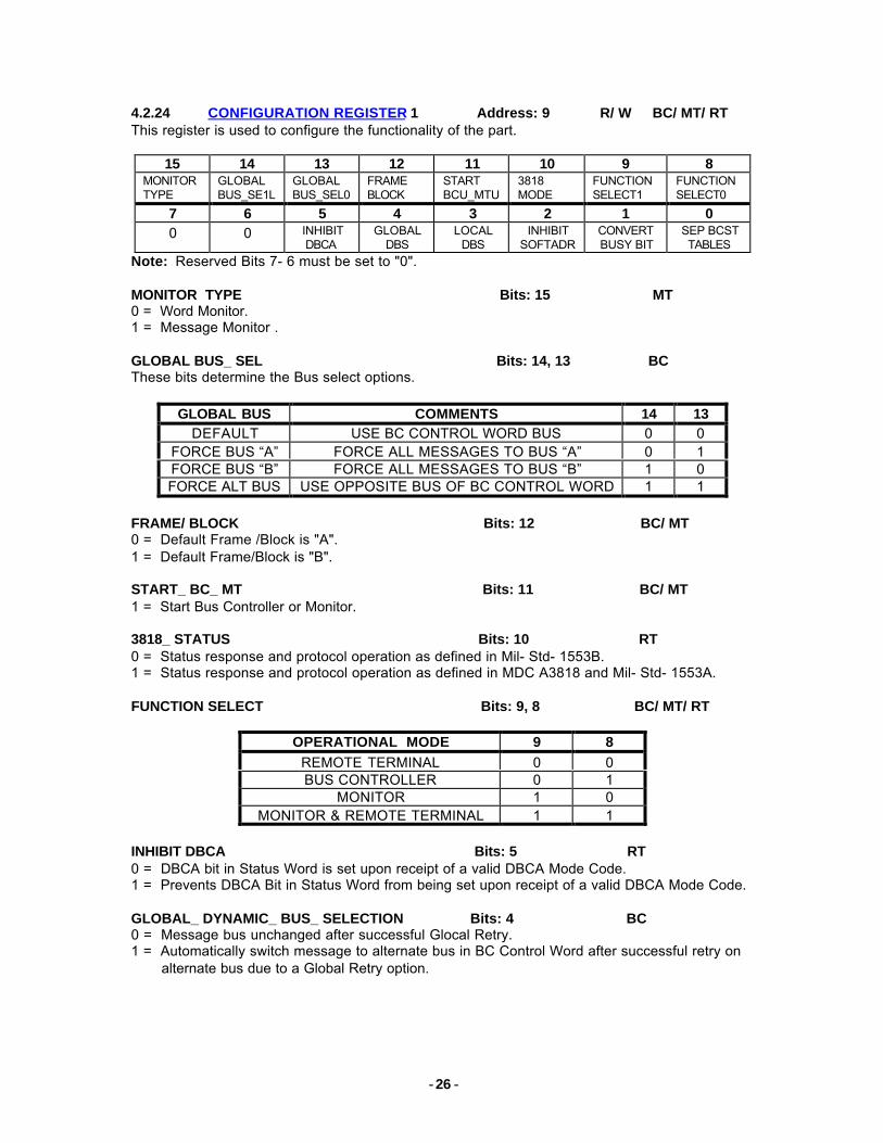
4.2.24 CONFIGURATION REGISTER 1 Address: 9 R/ W BC/ MT/ RTThis register is used to configure the functionality of the part.
15 14 13 12 11 10 9 8MONITORTYPE
GLOBALBUS_SE1L
GLOBALBUS_SEL0
FRAMEBLOCK
STARTBCU_MTU
3818MODE
FUNCTIONSELECT1
FUNCTIONSELECT0
7 6 5 4 3 2 1 00 0 INHIBIT
DBCAGLOBAL
DBSLOCAL
DBSINHIBIT
SOFTADRCONVERTBUSY BIT
SEP BCSTTABLES
Note: Reserved Bits 7- 6 must be set to "0".
MONITOR TYPE Bits: 15 MT0 = Word Monitor.1 = Message Monitor .
GLOBAL BUS_ SEL Bits: 14, 13 BCThese bits determine the Bus select options.
GLOBAL BUS COMMENTS 14 13DEFAULT USE BC CONTROL WORD BUS 0 0
FORCE BUS “A” FORCE ALL MESSAGES TO BUS “A” 0 1FORCE BUS “B” FORCE ALL MESSAGES TO BUS “B” 1 0FORCE ALT BUS USE OPPOSITE BUS OF BC CONTROL WORD 1 1
FRAME/ BLOCK Bits: 12 BC/ MT0 = Default Frame /Block is "A".1 = Default Frame/Block is "B".
START_ BC_ MT Bits: 11 BC/ MT1 = Start Bus Controller or Monitor.
3818_ STATUS Bits: 10 RT0 = Status response and protocol operation as defined in Mil- Std- 1553B.1 = Status response and protocol operation as defined in MDC A3818 and Mil- Std- 1553A.
FUNCTION SELECT Bits: 9, 8 BC/ MT/ RT
OPERATIONAL MODE 9 8REMOTE TERMINAL 0 0BUS CONTROLLER 0 1
MONITOR 1 0MONITOR & REMOTE TERMINAL 1 1
INHIBIT DBCA Bits: 5 RT0 = DBCA bit in Status Word is set upon receipt of a valid DBCA Mode Code.1 = Prevents DBCA Bit in Status Word from being set upon receipt of a valid DBCA Mode Code.
GLOBAL_ DYNAMIC_ BUS_ SELECTION Bits: 4 BC0 = Message bus unchanged after successful Glocal Retry.1 = Automatically switch message to alternate bus in BC Control Word after successful retry on alternate bus due to a Global Retry option.
- -27
LOCAL_ DYNAMIC_ BUS_ SELECTION Bits: 3 BC0 = Message bus unchanged after successful Local Retry.1 = Automatically switch message to alternate bus in BC Control Word after successful retry on alternate bus due to Local Retry option.
INHIBIT SOFT_ ADR Bits: 2 RT 0 = Bits (15: 11) of Basic Status Register set the RT Address when a Write Operation to that register is performed. The Hard Wired Address sets the RT Address at RESET.1 = Prevents software change of RT Address when writing to the Basic Status Register. Bits (15: 11) of Basic Status Register are “Don’t Care”. Only the Hard Wired Address sets the RT Address at RESET.
CONVERT BUSY BIT Bits: 1 RT0 = BUSY Bit is compliant with Mil- Std- 1553B.1 = Converts BUSY Bit to Non- 1553B operation. BUSY Bit becomes a standard bit with no special functionality. BUSY Bit is not set during software reset or MODE CODE_ 08 RESET.
SEP_ BCST_ TABLES Bits: 0 RT0 = Broadcast messages use the same pointers as receive message:. therefore, receive and broadcast messages are stored in the same data tables. The BCST bit in the tag word is used to differentiate between the two message types.1 = An additional 30 pointers are activated which puts receive and broadcast messages in separate data tables.
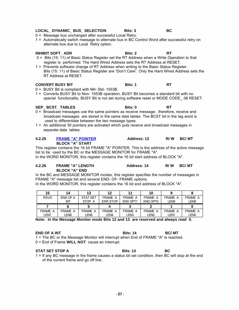
4.2.25 FRAME "A" POINTER Address: 13 R/ W BC/ MT BLOCK "A" STARTThis register contains the 16 bit FRAME "A" POINTER. This is the address of the active messagelist to be used by the BC or the MESSAGE MONITOR for FRAME "A".In the WORD MONITOR, this register contains the 16 bit start address of BLOCK "A".
4.2.26 FRAME "A" LENGTH Address: 14 R/ W BC/ MT BLOCK "A" ENDIn the BC and MESSAGE MONITOR modes, this register specifies the number of messages inFRAME "A" message list and several END- OF- FRAME options.In the WORD MONITOR, this register contains the 16 bit end address of BLOCK "A".
15 14 13 12 11 10 9 8RSVD END OF A
INTSTAT SETSTOP A
FRAME AERR STOP
FRAME AEND OPT1
FRAME AEND OPT0
FRAME ALEN9
FRAME ALEN8
7 6 5 4 3 2 1 0FRAME A
LEN7FRAME A
LEN6FRAME A
LEN5FRAME A
LEN4FRAME A
LEN3FRAME A
LEN2FRAME A
LEN1FRAME A
LEN0Note: In the Message Monitor mode Bits 12 and 13 are reserved and always read 0.
END OF A INT Bits: 14 BC/ MT1 = The BC or the Message Monitor will interrupt when End of FRAME "A" is reached.0 = End of Frame WILL NOT cause an interrupt.
STAT SET STOP A Bits: 13 BC1 = If any BC message in the frame causes a status bit set condition, then BC will stop at the end of the current frame and go off line.
- -28
FRAME A ERR STOP Bits: 12 BC1 = If any BC message in the frame causes an error condition, then BC will stop at the end of the current frame and go off line.
FRAME A END OPT Bits: 11, 10 BC/ MTThese two bits determine a course of action at the end of FRAME "A" in the Message Monitor.
FRAME A END OPTIONS 11 10STOP AT END OF FRAME A 0 0REPEAT FRAME A 0 1GOTO FRAME B 1 0STOP AT END OF FRAME A 1 1
FRAME A LENGTH Bits: 9: 0 BC/ MTThese ten bits determine the number of messages that the frame will contain, up to a maximumof 1023.
4.2.27 FRAME "B" POINTER Address: 16 R/ W BC/ MT BLOCK "B" STARTThis register contains the 16 bit FRAME "B" POINTER. This is the address of the active messagelist to be used by the BC or the MESSAGE MONITOR for FRAME "B".In the WORD MONITOR, this register contains the 16 bit start address of BLOCK "B".
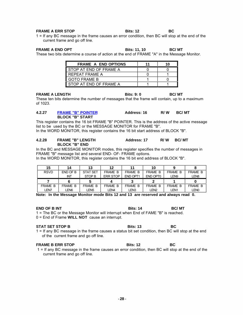
4.2.28 FRAME "B" LENGTH Address: 17 R/ W BC/ MT BLOCK "B" ENDIn the BC and MESSAGE MONITOR modes, this regiater specifies the number of messages inFRAME "B" message list and several END- OF- FRAME options.In the WORD MONITOR, this register contains the 16 bit end address of BLOCK "B".
15 14 13 12 11 10 9 8RSVD END OF B
INTSTAT SETSTOP B
FRAME BERR STOP
FRAME BEND OPT1
FRAME BEND OPT0
FRAME BLEN9
FRAME BLEN8
7 6 5 4 3 2 1 0FRAME B
LEN7FRAME B
LEN6FRAME B
LEN5FRAME B
LEN4FRAME B
LEN3FRAME B
LEN2FRAME B
LEN1FRAME B
LEN0Note: In the Message Monitor mode Bits 12 and 13 are reserved and always read 0.
END OF B INT Bits: 14 BC/ MT1 = The BC or the Message Monitor will interrupt when End of FAME "B" is reached.0 = End of Frame WILL NOT cause an interrupt.
STAT SET STOP B Bits: 13 BC1 = If any BC message in the frame causes a status bit set condition, then BC will stop at the end of the current frame and go off line.
FRAME B ERR STOP Bits: 12 BC 1 = If any BC message in the frame causes an error condition, then BC will stop at the end of the current frame and go off line.
- -29
FRAME B END OPT Bits: 11, 10 BC/ MTThese two bits determine a course of action at the end of FRAME "B" in the Message monitor.
FRAME B END OPTIONS 11 10STOP AT END OF FRAME B 0 0REPEAT FRAME B 0 1GOTO FRAME A 1 0STOP AT END OF FRAME B 1 1
FRAME B LENGTH Bits: 9: 0 BC/ MTThese ten bits determine the number of messages that the frame will contain, up to a maximumof 1023.
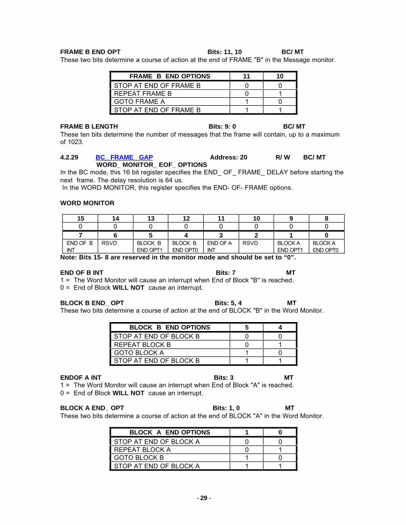
4.2.29 BC_ FRAME_ GAP Address: 20 R/ W BC/ MT WORD_ MONITOR_ EOF_ OPTIONSIn the BC mode, this 16 bit register specifies the END_ OF_ FRAME_ DELAY before starting thenext frame. The delay resolution is 64 us. In the WORD MONITOR, this register specifies the END- OF- FRAME options.
WORD MONITOR
15 14 13 12 11 10 9 80 0 0 0 0 0 0 07 6 5 4 3 2 1 0
END OF BINT
RSVD BLOCK BEND OPT1
BLOCK BEND OPT0
END OF AINT
RSVD BLOCK AEND OPT1
BLOCK AEND OPT0
Note: Bits 15- 8 are reserved in the monitor mode and should be set to “0”.
END OF B INT Bits: 7 MT1 = The Word Monitor will cause an interrupt when End of Block "B" is reached.0 = End of Block WILL NOT cause an interrupt.
BLOCK B END_ OPT Bits: 5, 4 MTThese two bits determine a course of action at the end of BLOCK "B" in the Word Monitor.
BLOCK B END OPTIONS 5 4STOP AT END OF BLOCK B 0 0REPEAT BLOCK B 0 1GOTO BLOCK A 1 0STOP AT END OF BLOCK B 1 1
ENDOF A INT Bits: 3 MT1 = The Word Monitor will cause an interrupt when End of Block "A" is reached.0 = End of Block WILL NOT cause an interrupt.
BLOCK A END_ OPT Bits: 1, 0 MTThese two bits determine a course of action at the end of BLOCK "A" in the Word Monitor.
BLOCK A END OPTIONS 1 0STOP AT END OF BLOCK A 0 0REPEAT BLOCK A 0 1GOTO BLOCK B 1 0STOP AT END OF BLOCK A 1 1
- -30
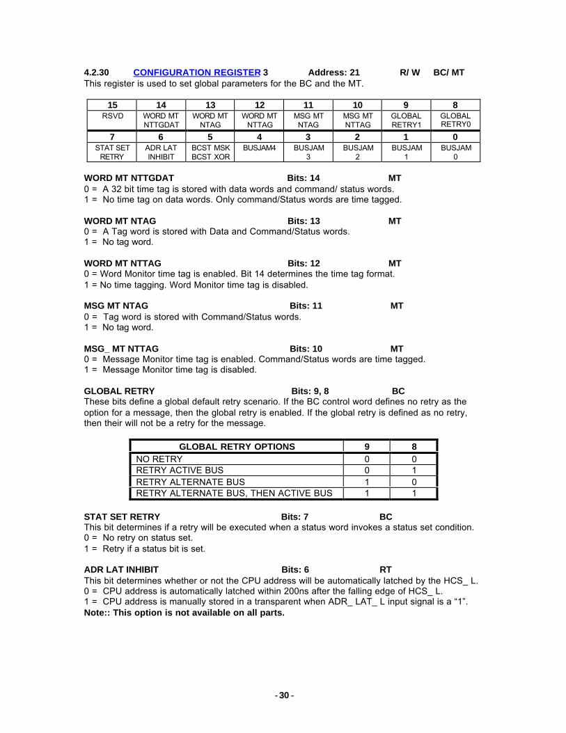
4.2.30 CONFIGURATION REGISTER 3 Address: 21 R/ W BC/ MTThis register is used to set global parameters for the BC and the MT.
15 14 13 12 11 10 9 8RSVD WORD MT
NTTGDATWORD MT
NTAGWORD MT
NTTAGMSG MTNTAG
MSG MTNTTAG
GLOBALRETRY1
GLOBALRETRY0
7 6 5 4 3 2 1 0STAT SET
RETRYADR LATINHIBIT
BCST MSKBCST XOR
BUSJAM4 BUSJAM3
BUSJAM2
BUSJAM1
BUSJAM0
WORD MT NTTGDAT Bits: 14 MT0 = A 32 bit time tag is stored with data words and command/ status words.1 = No time tag on data words. Only command/Status words are time tagged.
WORD MT NTAG Bits: 13 MT0 = A Tag word is stored with Data and Command/Status words.1 = No tag word.
WORD MT NTTAG Bits: 12 MT0 = Word Monitor time tag is enabled. Bit 14 determines the time tag format.1 = No time tagging. Word Monitor time tag is disabled.
MSG MT NTAG Bits: 11 MT0 = Tag word is stored with Command/Status words.1 = No tag word.
MSG_ MT NTTAG Bits: 10 MT0 = Message Monitor time tag is enabled. Command/Status words are time tagged.1 = Message Monitor time tag is disabled.
GLOBAL RETRY Bits: 9, 8 BCThese bits define a global default retry scenario. If the BC control word defines no retry as theoption for a message, then the global retry is enabled. If the global retry is defined as no retry,then their will not be a retry for the message.
GLOBAL RETRY OPTIONS 9 8NO RETRY 0 0RETRY ACTIVE BUS 0 1RETRY ALTERNATE BUS 1 0RETRY ALTERNATE BUS, THEN ACTIVE BUS 1 1
STAT SET RETRY Bits: 7 BCThis bit determines if a retry will be executed when a status word invokes a status set condition.0 = No retry on status set.1 = Retry if a status bit is set.
ADR LAT INHIBIT Bits: 6 RTThis bit determines whether or not the CPU address will be automatically latched by the HCS_ L.0 = CPU address is automatically latched within 200ns after the falling edge of HCS_ L.1 = CPU address is manually stored in a transparent when ADR_ LAT_ L input signal is a “1”.Note:: This option is not available on all parts.
- -31
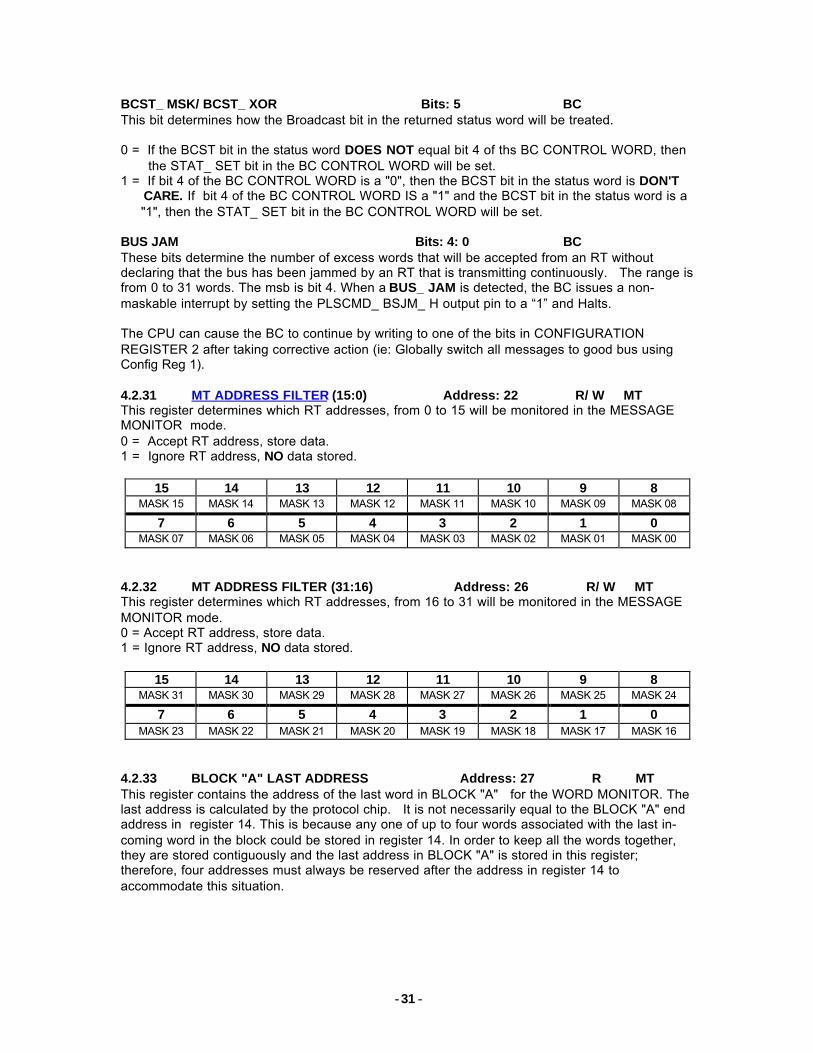
BCST_ MSK/ BCST_ XOR Bits: 5 BCThis bit determines how the Broadcast bit in the returned status word will be treated.
0 = If the BCST bit in the status word DOES NOT equal bit 4 of ths BC CONTROL WORD, then the STAT_ SET bit in the BC CONTROL WORD will be set.1 = If bit 4 of the BC CONTROL WORD is a "0", then the BCST bit in the status word is DON'T CARE. If bit 4 of the BC CONTROL WORD IS a "1" and the BCST bit in the status word is a "1", then the STAT_ SET bit in the BC CONTROL WORD will be set.
BUS JAM Bits: 4: 0 BCThese bits determine the number of excess words that will be accepted from an RT withoutdeclaring that the bus has been jammed by an RT that is transmitting continuously. The range isfrom 0 to 31 words. The msb is bit 4. When a BUS_ JAM is detected, the BC issues a non-maskable interrupt by setting the PLSCMD_ BSJM_ H output pin to a “1” and Halts.
The CPU can cause the BC to continue by writing to one of the bits in CONFIGURATIONREGISTER 2 after taking corrective action (ie: Globally switch all messages to good bus usingConfig Reg 1).
4.2.31 MT ADDRESS FILTER (15:0) Address: 22 R/ W MTThis register determines which RT addresses, from 0 to 15 will be monitored in the MESSAGEMONITOR mode.0 = Accept RT address, store data.1 = Ignore RT address, NO data stored.
15 14 13 12 11 10 9 8MASK 15 MASK 14 MASK 13 MASK 12 MASK 11 MASK 10 MASK 09 MASK 08
7 6 5 4 3 2 1 0MASK 07 MASK 06 MASK 05 MASK 04 MASK 03 MASK 02 MASK 01 MASK 00
4.2.32 MT ADDRESS FILTER (31:16) Address: 26 R/ W MTThis register determines which RT addresses, from 16 to 31 will be monitored in the MESSAGEMONITOR mode.0 = Accept RT address, store data.1 = Ignore RT address, NO data stored.
15 14 13 12 11 10 9 8MASK 31 MASK 30 MASK 29 MASK 28 MASK 27 MASK 26 MASK 25 MASK 24
7 6 5 4 3 2 1 0MASK 23 MASK 22 MASK 21 MASK 20 MASK 19 MASK 18 MASK 17 MASK 16
4.2.33 BLOCK "A" LAST ADDRESS Address: 27 R MTThis register contains the address of the last word in BLOCK "A" for the WORD MONITOR. Thelast address is calculated by the protocol chip. It is not necessarily equal to the BLOCK "A" endaddress in register 14. This is because any one of up to four words associated with the last in-coming word in the block could be stored in register 14. In order to keep all the words together,they are stored contiguously and the last address in BLOCK "A" is stored in this register;therefore, four addresses must always be reserved after the address in register 14 toaccommodate this situation.
- -32
4.2.34 BLOCK "B" LAST ADDRESS Address: 28 R MTThis register contains the address of the last word in BLOCK "B" for the WORD MONITOR. Thelast address is calculated by the protocol chip. It is not necessarily equal to the BLOCK "B"end address in register 17. This is because any one of up to four words associated with the lastin- coming word in the block could be stored in register 17. In order to keep all the wordstogether, they are stored contiguously and the last address in BLOCK "B" is stored in thisregister; therefore, four addresses must always be reserved after the address in register 17 toaccommodate this situation.
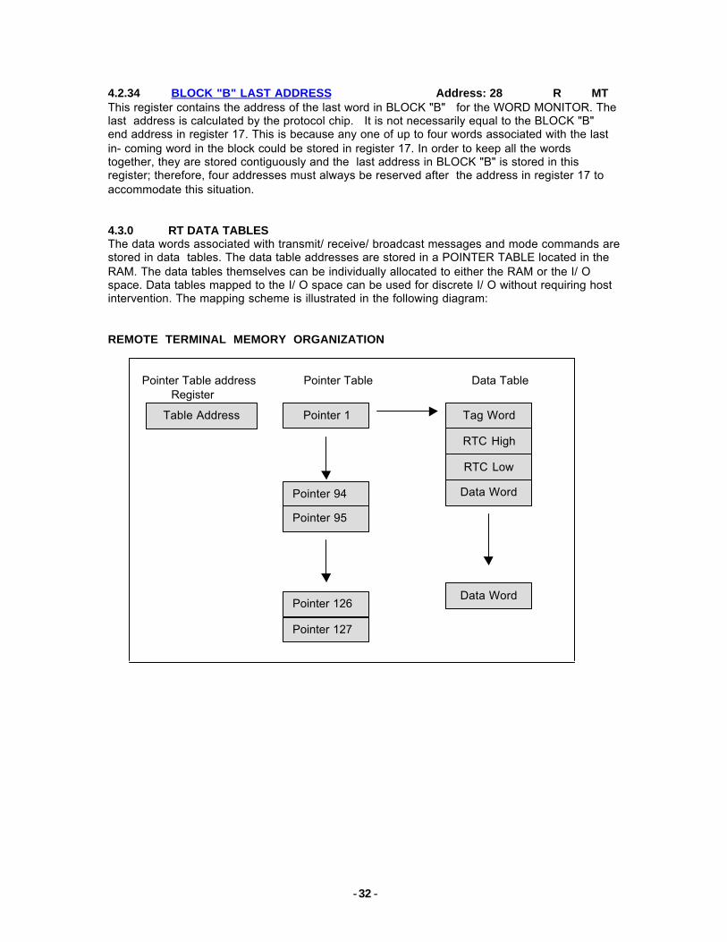
4.3.0 RT DATA TABLESThe data words associated with transmit/ receive/ broadcast messages and mode commands arestored in data tables. The data table addresses are stored in a POINTER TABLE located in theRAM. The data tables themselves can be individually allocated to either the RAM or the I/ Ospace. Data tables mapped to the I/ O space can be used for discrete I/ O without requiring hostintervention. The mapping scheme is illustrated in the following diagram:
REMOTE TERMINAL MEMORY ORGANIZATION
Pointer Table address Pointer Table Data Table Register
Pointer 1
Pointer 94
Pointer 95
Pointer 126
Pointer 127
RTC High
Tag Word
RTC Low
Data Word
Data Word
Table Address
- -33
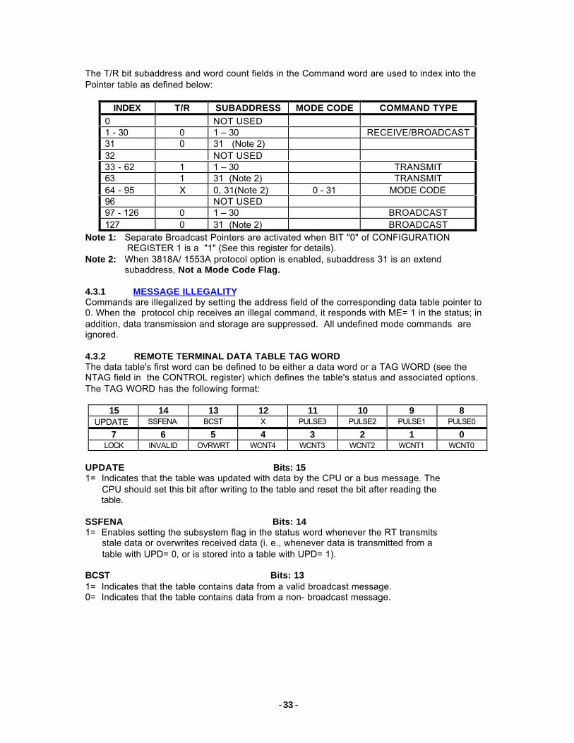
The T/R bit subaddress and word count fields in the Command word are used to index into thePointer table as defined below:
INDEX T/R SUBADDRESS MODE CODE COMMAND TYPE0 NOT USED1 - 30 0 1 – 30 RECEIVE/BROADCAST31 0 31 (Note 2)32 NOT USED33 - 62 1 1 – 30 TRANSMIT63 1 31 (Note 2) TRANSMIT64 - 95 X 0, 31(Note 2) 0 - 31 MODE CODE96 NOT USED97 - 126 0 1 – 30 BROADCAST127 0 31 (Note 2) BROADCAST
Note 1: Separate Broadcast Pointers are activated when BIT "0" of CONFIGURATION REGISTER 1 is a "1" (See this register for details).Note 2: When 3818A/ 1553A protocol option is enabled, subaddress 31 is an extend subaddress, Not a Mode Code Flag.
4.3.1 MESSAGE ILLEGALITYCommands are illegalized by setting the address field of the corresponding data table pointer to0. When the protocol chip receives an illegal command, it responds with ME= 1 in the status; inaddition, data transmission and storage are suppressed. All undefined mode commands areignored.
4.3.2 REMOTE TERMINAL DATA TABLE TAG WORDThe data table's first word can be defined to be either a data word or a TAG WORD (see theNTAG field in the CONTROL register) which defines the table's status and associated options.The TAG WORD has the following format:
15 14 13 12 11 10 9 8UPDATE SSFENA BCST X PULSE3 PULSE2 PULSE1 PULSE0
7 6 5 4 3 2 1 0LOCK INVALID OVRWRT WCNT4 WCNT3 WCNT2 WCNT1 WCNT0
UPDATE Bits: 151= Indicates that the table was updated with data by the CPU or a bus message. The CPU should set this bit after writing to the table and reset the bit after reading the table.
SSFENA Bits: 141= Enables setting the subsystem flag in the status word whenever the RT transmits stale data or overwrites received data (i. e., whenever data is transmitted from a table with UPD= 0, or is stored into a table with UPD= 1).
BCST Bits: 131= Indicates that the table contains data from a valid broadcast message.0= Indicates that the table contains data from a non- broadcast message.
- -34
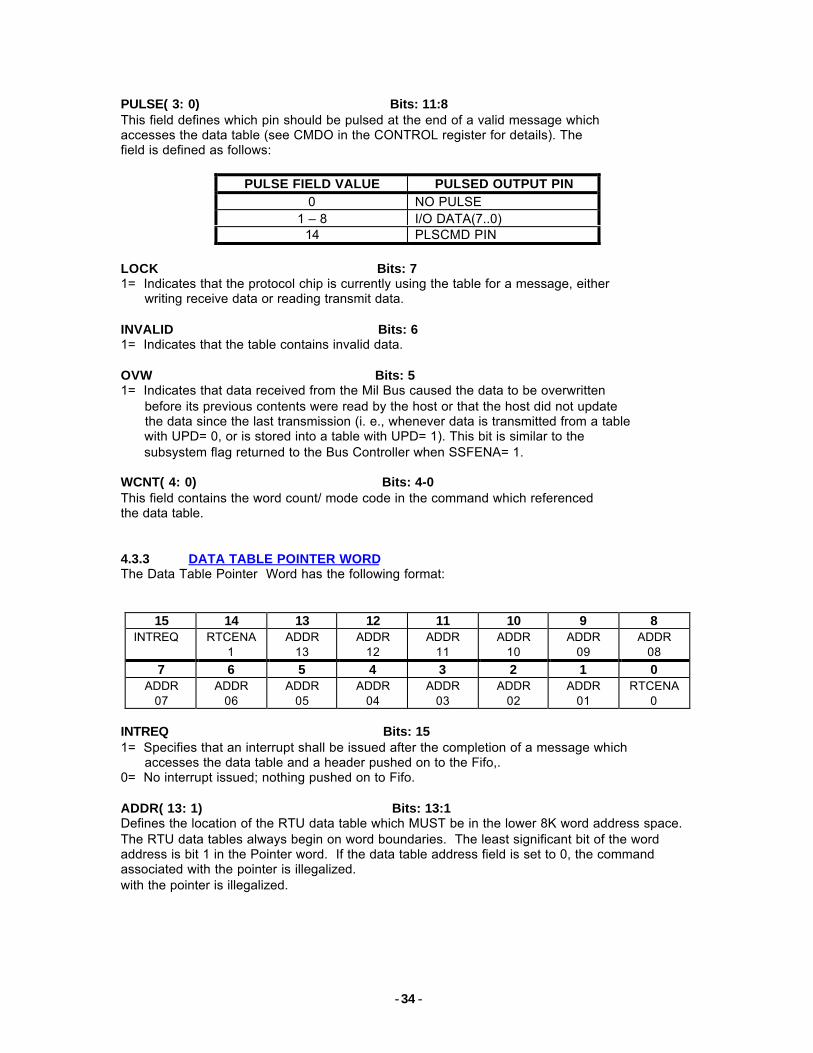
PULSE( 3: 0) Bits: 11:8This field defines which pin should be pulsed at the end of a valid message whichaccesses the data table (see CMDO in the CONTROL register for details). Thefield is defined as follows:
PULSE FIELD VALUE PULSED OUTPUT PIN0 NO PULSE
1 – 8 I/O DATA(7..0)14 PLSCMD PIN
LOCK Bits: 71= Indicates that the protocol chip is currently using the table for a message, either writing receive data or reading transmit data.
INVALID Bits: 61= Indicates that the table contains invalid data.
OVW Bits: 51= Indicates that data received from the Mil Bus caused the data to be overwritten before its previous contents were read by the host or that the host did not update the data since the last transmission (i. e., whenever data is transmitted from a table with UPD= 0, or is stored into a table with UPD= 1). This bit is similar to the subsystem flag returned to the Bus Controller when SSFENA= 1.
WCNT( 4: 0) Bits: 4-0This field contains the word count/ mode code in the command which referencedthe data table.
4.3.3 DATA TABLE POINTER WORDThe Data Table Pointer Word has the following format:
15 14 13 12 11 10 9 8INTREQ RTCENA
1ADDR
13ADDR
12ADDR
11ADDR
10ADDR
09ADDR
087 6 5 4 3 2 1 0
ADDR07
ADDR06
ADDR05
ADDR04
ADDR03
ADDR02
ADDR01
RTCENA0
INTREQ Bits: 151= Specifies that an interrupt shall be issued after the completion of a message which accesses the data table and a header pushed on to the Fifo,.0= No interrupt issued; nothing pushed on to Fifo.
ADDR( 13: 1) Bits: 13:1Defines the location of the RTU data table which MUST be in the lower 8K word address space.The RTU data tables always begin on word boundaries. The least significant bit of the wordaddress is bit 1 in the Pointer word. If the data table address field is set to 0, the commandassociated with the pointer is illegalized.with the pointer is illegalized.
- -35
RTCENA Bits: 14,0Real Time Clock Time Tag Message Oprions. The Time_ Tag_ Transmit option will cause the firsttwo transmitted words of the associated Transmit Command to contain the time tag, MSW first.
TIME TAG MODE 14 0NO TIME TAG ON MESSAGES 0 0NO TIME TAG ON MESSAGES 0 1TIME TAG MESSAGES; DON’T TRANSMIT TIME TAG WITH TRANSMITCOMMAND
1 0
TIME TAG MESSAGES; TRANSMIT TIME TAG WITH TRANSMITCOMMAND
1 1
Note: If the No Time Tag option is used, data words occupy the time tag positions.
4.3.4 RT DATA TABLE BUFFERING SCHEMESince the host and the NHi_ ET can access data tables asynchronously, data integrity must beensured by a suitable buffering scheme. The method employed by the ET assumes that there aretwo pointer tables; one specifies data tables accessed by the ET and the other tables accessedby the host. The host's pointer table can reside anywhere in its memory space since it is neveraccessed by the ET. Data buffers are switched by the host exchanging pointers as explainedbelow.
4.3.4.1 RT RAM ACCESSWhen the ET wants to read or write to a data table, it fetches the corresponding data table pointerfrom its pointer table. It then sets the LOCK bit in the data table's TAG WORD to 1 and proceedswith the update. At the completion of the update, the ET sets the LOCK bit to 0 and also sets theUPDATE bit in the TAG WORD to 1 if it wrote to the data table or 0 if it read the data table. If thecondition of the UPDATE bit at the start of the ET access indicates that the host has not readfrom or written to the data table since the last ET access to that table, the ET sets the OVRWRTbit in the TAG WORD to 1 to tell the host stale data has been transmitted by the ET or data hasbeen overwritten by the ET.
Since the ET may fetch a data table pointer while the host is in the process of exchanging thecorresponding pointers, there is a possibility that the ET's pointer will point to the table used bythe host. In order to avoid this potential conflict, the host should check the LOCK bit in its datatable tag word AFTER exchanging the pointers but BEFORE reading the data. If LOCK= 1, thehost should wait until the protocol chip sets LOCK= 0.
NOTE: The LOCK bit is ALWAYS set in the TAG WORD of the data table accessed by the ET,irrespective of when the pointers are exchanged by the host. This is guaranteed because the ETreads the data table's pointer and sets the LOCK bit in the TAG WORD using a read - read -modify - write sequence which cannot be interrupted by the host (i. e., read POINTER - read TAGWORD - modify LOCK bit - write back TAG WORD with LOCK bit modified).
4.3.4.2 HOST RAM ACCESS
RECEIVE DATA TABLEWhen the host wants to read the data in a RECEIVE data table, it FIRST EXCHANGES thepointer in its pointer table with the corresponding pointer in the ET's table. Then, the host readsthe LOCK bit in the TAG WORD. If the LOCK bit is 0, the host proceeds with its access. If,however, the LOCK bit is 1, this informs the host that the ET is accessing that data table. Thehost should then delay its access until the LOCK bit has been set to 0 by the ET. When the hostfinishes accessing the RECEIVE data table, it should clear the UPD bit in the data table's TAGWORD to 0. This will tell the ET the host has taken the data.
- -36
TRANSMIT DATA TABLEWhen the host wants to write data to a TRANSMIT data table, the apparent method would be toload the table with data then exchange corresponding pointers. There is a subtle problem withthis approach. If the host had, within a short period of time prior to this exchange previouslyloaded and exchanged these same pointers while the ET had been transmitting data from thatdata table , the LOCK bit could still be set in the table the the host was loading during the secondsequence. This is possible because it can take up to 640us to transmit a message, the LOCK bitbeing set for the entire time. This could cause new data to be mixed with old data andtransmitted. Avoiding this potential problem is quite simple.
When the host wants to access a TRANSMIT data table, it first reads the LOCK bit in the TAGWORD of the table belonging to the host. If the LOCK bit is 0, the host proceeds with its accessand loads the data table . If, however, the LOCK bit is 1, this informs the host that the ET is stillaccessing that data table. The host should then delay its access until the LOCK bit has been setto 0 by the ET. When the host finishes updating its TRANSMIT data table, it should set the UPDbit in the data table's TAG WORD to 1 and then exchange corresponding pointers. This willensure that updated data for transmission is made available to the ET as soon as possible andinform the ET that it will be transmitting fresh data.
Since the host can change its table of pointers at any time, the above mapping scheme can beused to achieve any desired depth of buffering by simply employing a "round- robin" of pointers.
4.3.4.3 READ- MODIFY- WRITEThe host Read- Modify- Write cycle is used to support CPUs similar to the Motorola 680X0 wherecertain instructions (eg:, test and set) require two contiguous accesses to memory. Suchaccesses are unique in that the address remains active for both cycles.
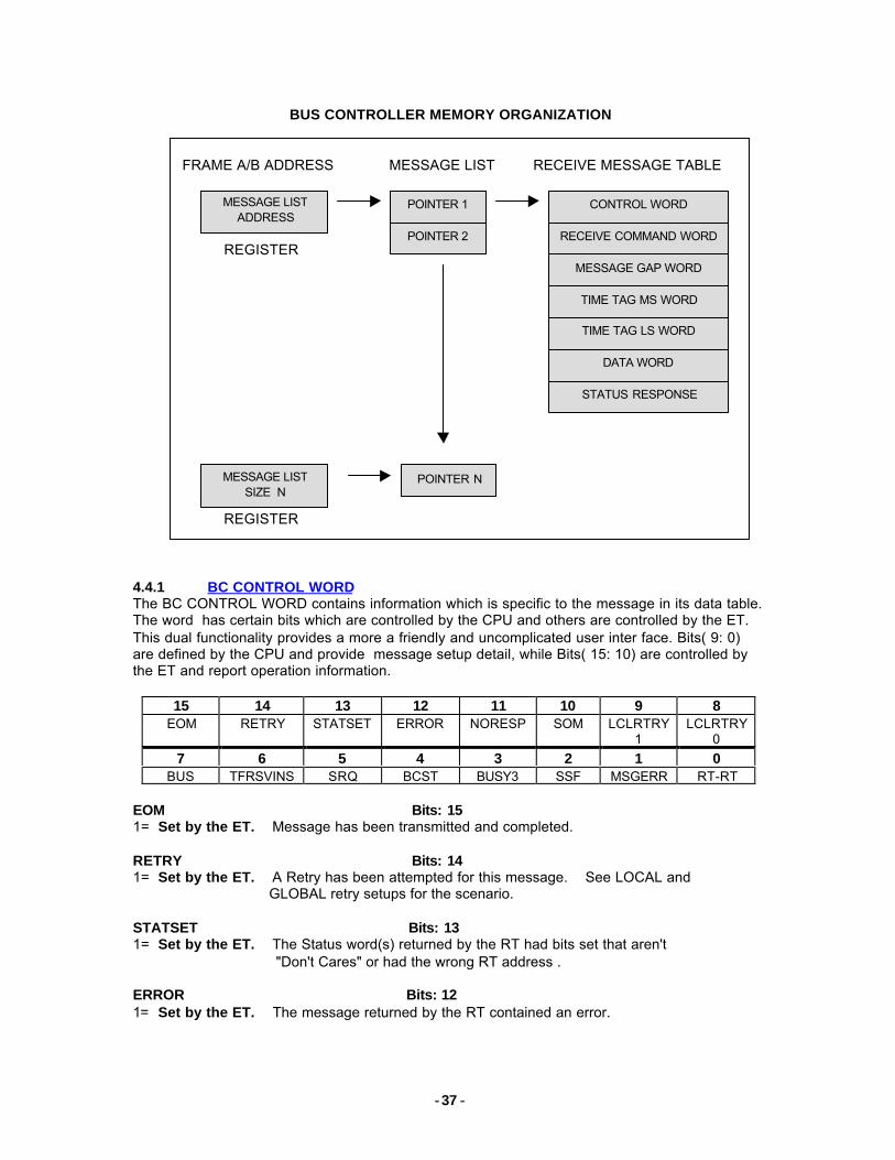
4.4.0 BUS CONTROLLER MESSAGE LISTS AND DATA TABLESThe BC is organized and controlled by message lists. Each message list contains the addressesof data tables associated with the list. A message list can contain up to a maximum of 1023 16bit addresses. The number of message lists and data tables is limited only by the size of the ram.The message list mapping scheme is illustrated in the following diagram.. FRAME A/ BPOINTER and FRAME A/ B LENGTH registers have been discussed in a previous section. Seedetails.
The CPU loads each message list with number of message table pointers determined by a givenscenario requirement. The list is activated by placing its address in the FRAME A or FRAME BPOINTER register and the number of pointers in the list in the corresponding FRAME LENGTHregister.
- -37
BUS CONTROLLER MEMORY ORGANIZATION
FRAME A/B ADDRESS MESSAGE LIST RECEIVE MESSAGE TABLE
REGISTER
REGISTER
4.4.1 BC CONTROL WORDThe BC CONTROL WORD contains information which is specific to the message in its data table.The word has certain bits which are controlled by the CPU and others are controlled by the ET.This dual functionality provides a more a friendly and uncomplicated user inter face. Bits( 9: 0)are defined by the CPU and provide message setup detail, while Bits( 15: 10) are controlled bythe ET and report operation information.
15 14 13 12 11 10 9 8EOM RETRY STATSET ERROR NORESP SOM LCLRTRY
1LCLRTRY
07 6 5 4 3 2 1 0
BUS TFRSVINS SRQ BCST BUSY3 SSF MSGERR RT-RT
EOM Bits: 151= Set by the ET. Message has been transmitted and completed.
RETRY Bits: 141= Set by the ET. A Retry has been attempted for this message. See LOCAL and GLOBAL retry setups for the scenario.
STATSET Bits: 131= Set by the ET. The Status word(s) returned by the RT had bits set that aren't "Don't Cares" or had the wrong RT address .
ERROR Bits: 121= Set by the ET. The message returned by the RT contained an error.
MESSAGE LISTADDRESS
POINTER 2
POINTER 1 CONTROL WORD
RECEIVE COMMAND WORD
MESSAGE GAP WORD
TIME TAG MS WORD
TIME TAG LS WORD
DATA WORD
STATUS RESPONSE
POINTER NMESSAGE LISTSIZE N
- -38
NORESP Bits: 111= Set by the ET. The RT DID NOT respond with a Status or data as expected.SOM Bits: 101= Set by the ET. The message is currently active. The ET could be transmitting, waiting for a response or receiving.
LOCAL_ RETRY Bits: 9,8Set by the CPU. Bits( 9: 8) define a local specific retry scenario. If the BC control word defines no retry as the option for the message, then the global retry is enabled. If the global retry is defined as no retry, then their will not be a retry for the message.
LOCAL RETRY OPTIONS 9 8NO RETRY 0 0RETRY ACTIVE BUS 0 1RETRY ALTERNATE BUS 1 0RETRY ALTERNATE BUS, THEN ACTIVE BUS 1 1
BUS Bits: 70= Set by CPU & ET. Message will use BUS A.1= Set by CPU & ET Message will use BUS B. This bit defines the bus that the message will use. This bus setting, however, can be overridden by the settings in CONFIGURATION 1. See this register for specific details.
TFRSVINS Bits: 60= Set by the CPU. The value of the Terminal Flag bit, the Reserved bits, and the Instrumentation bit are treated as "Don't Care", and will NOT cause the STATSET bit to be set no matter what their value in the returned Status word.1= Set by the CPU The STATSET bit will be set if the Terminal Flag bit, or one of the Reservedbits or the instrumentation bit is set in the returned Status word.
SRQ Bits: 50= Set by the CPU. The value of the Service Request bit is treated as "Don't Care", and will NOT cause the STASET bit to be set no matter what its value in the returned Status word.1= Set by the CPU. The STATSET bit will be set if the Service Request bit is set in the returned Status word.
BCST Bits: 4Set by the CPU. The operation of this bit is determined by bit 5 of CONFIGURATION REGISTER 3. This bit will either be used as a mask or an xor flag for the Broadcast Received bit in the returned status word.
CONFIGURATION REG 3 Bit 05 = 0 (BCST bit is an Xor Flag):If the Broadcast Received bit in the returned status word DOES NOT equal the BCST bit of theBC CONTROL WORD, then the STATSET bit in the BC CONTROL WORD will be set.
CONFIGURATION REG 3 Bit 05 = 1 (BCST bit is a Mask):0= The value of the Broadcast Received bit is treated as "Don't Care", and will NOT cause the STATSET bit to be set no matter what its value in the returned Status word.1= The STATSET bit will be set if the Broadcast Received bit is set in the returned Status word.
- -39
BUSY Bits: 30= Set by the CPU. The value of the Busy bit is treated as "Don't Care", and will NOT cause the STATSET bit to be set no matter what its value in the returned Status word.1= Set by the CPU. The STATSET bit will be set if the Busy bit is set in the returned Status word.
SSF Bits: 20= Set by the CPU. The value of the Subsystem Flag bit is treated as "Don't Care", and will NOT cause the STATSET bit to be set no matter what its value in the returned Status word.1= Set by the CPU. The STATSET bit will be set if the Subsystem Flag bit is set in the returned Status word.
MSGERR Bits: 10= Set by the CPU. The value of the Message Error bit is treated as "Don't Care", and will NOT cause the STATSET bit to be set no matter what its value in the returned Status word.1= Set by the CPU. The STATSET bit will be set if the Message Error bit is set in the returned Status word.
RT_ RT Bits: 00= Set by the CPU. Message is NOT an RT to RT command.1= Set by the CPU. Message IS an RT to RT command.
Note: Status bits treated as "Don't Cares" will NOT cause a STAT_SET.
4.4.2 BC COMMAND WORDThis is the 16 bit Command word that defines the message type as defined by the Mil-Bus.
4.4.3 BC MESSAGE GAP WORDThe BC MESSAGE GAP WORD contains additional information which is specific to the messagein its data table. The word sets the gap time delay to the start of the next message in the list, endof message stop conditions, the message interrupt and a NOP feature. The resolution of theGap counter is 1us and the maximum gap is 4ms. NOP's can be used to extend the inter-message gap beyond the 4ms maximum which is allowed by the Gap field.
15 14 13 12 11 10 9 8NOP EOM_INT STATSTP ERRSTP GAP11 GAP10 GAP09 GAP08
7 6 5 4 3 2 1 0GAP07 GAP06 GAP05 GAP04 GAP03 GAP02 GAP01 GAP00
NOP Bits: 150= Send message as defined.1= Do NOT send message. Start Gap Timer and wait till time out, then GoTo next message.Note: If the last message in a frame is a NOP(bit 15 = '1'), the E-O-F interrupt is disabled and any interrupts associated with that NOP message are disabled.
EOM_INT Bits: 140= No interrupt at End- of- Message.1= Interrupt at End- of- Message.
- -40
STATSTP Bits: 130= Ignore a Status Set condition in the returned RT status word for the message.1= Halt and go off- line if a Status Set condition is detected in the returned RT status word for the message.ERRSTP Bits: 120= Ignore the Error condition in the message.1= Halt and go off- line if an Error is detected in the message.
GAP Bits: 11: 0This field sets the inter-message Gap Time delay. The resolution is 1us and the range of thedelay is 0 to 4ms. The start of the next message in the list is delayed by this interval.
4.4.4 BC TIME TAG MS WORDThis word contains the upper 16 bits of the 32 bit Time Tag.
4.4.5 BC TIME TAG LS WORDThis word contains the lower 16 bits of the 32 bit Time Tag.
4.4.6 BC DATA WORDThis space contains from 1 to 32 data words which are associated with the message.
4.4.7 BC STATUS RESPONSEThis space contains the Status response from the RT
4.4.8 BUS CONTROLLER MESSAGESThe following table illustrates all the message table formats used in the Bus Controller. Noticethat all the components of a message table are located in contiguous ram locations. Thisreduces CPU overhead and simplifies software development.
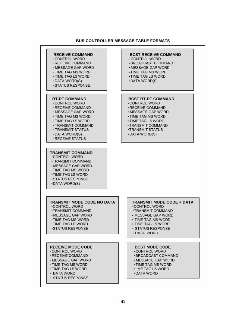
- -41
BUS CONTROLLER MESSAGE TABLE FORMATS
RECEIVE COMMAND BCST RECEIVE COMMAND •CONTROL WORD •CONTROL WORD •RECEIVE COMMAND •BROADCAST COMMAND •MESSAGE GAP WORD •MESSAGE GAP WORD •TIME TAG MS WORD •TIME TAG MS WORD •TIME TAG LS WORD •TIME TAG LS WORD •DATA WORD(S) •DATA WORD(S) •STATUS RESPONSE
RT-RT COMMAND BCST RT-RT COMMAND •CONTROL WORD •CONTROL WORD •RECEIVE COMMAND •RECEIVE COMMAND •MESSAGE GAP WORD •MESSAGE GAP WORD •TIME TAG MS WORD •TIME TAG MS WORD •TIME TAG LS WORD •TIME TAG LS WORD •TRANSMIT COMMAND •TRANSMIT COMMAND •TRANSMIT STATUS •TRANSMIT STATUS •DATA WORD(S) •DATA WORD(S) •RECEIVE STATUS
TRANSMIT COMMAND •CONTROL WORD •TRANSMIT COMMAND •MESSAGE GAP WORD •TIME TAG MS WORD •TIME TAG LS WORD •STATUS RESPONSE •DATA WORD(S)
TRANSMIT MODE CODE NO DATA TRANSMIT MODE CODE + DATA •CONTROL WORD •CONTROL WORD •TRANSMIT COMMAND •TRANSMIT COMMAND •MESSAGE GAP WORD • MESSAGE GAP WORD •TIME TAG MS WORD • TIME TAG MS WORD •TIME TAG LS WORD • TIME TAG LS WORD •STATUS RESPONSE • STATUS RESPONSE • DATA WORD
RECEIVE MODE CODE BCST MODE CODE •CONTROL WORD •CONTROL WORD •RECEIVE COMMAND •BROADCAST COMMAND •MESSAGE GAP WORD •MESSAGE GAP WORD •TIME TAG MS WORD •TIME TAG MS WORD •TIME TAG LS WORD • IME TAG LS WORD • DATA WORD •DATA WORD • STATUS RESPONSE
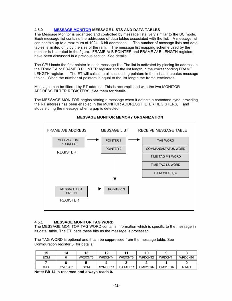
- -42
4.5.0 MESSAGE MONITOR MESSAGE LISTS AND DATA TABLESThe Message Monitor is organized and controlled by message lists, very similar to the BC mode.Each message list contains the addresses of data tables associated with the list. A message listcan contain up to a maximum of 1024 16 bit addresses. The number of message lists and datatables is limited only by the size of the ram. The message list mapping scheme used by themonitor is illustrated in the figure. FRAME A/ B POINTER and FRAME A/ B LENGTH registershave been discussed in a previous section. See details.
The CPU loads the first pointer in each message list. The list is activated by placing its address inthe FRAME A or FRAME B POINTER register and the list length in the corresponding FRAMELENGTH register. The ET will calculate all succeeding pointers in the list as it creates messagetables . When the number of pointers is equal to the list length the frame terminates.
Messages can be filtered by RT address. This is accomplished with the two MONITORADDRESS FILTER REGISTERS. See them for details.
The MESSAGE MONITOR begins storing a message when it detects a command sync, providingthe RT address has been enabled in the MONITOR ADDRESS FILTER REGISTERS, andstops storing the message when a gap is detected.
MESSAGE MONITOR MEMORY ORGANIZATION
FRAME A/B ADDRESS MESSAGE LIST RECEIVE MESSAGE TABLE
REGISTER
REGISTER
4.5.1 MESSAGE MONITOR TAG WORDThe MESSAGE MONITOR TAG WORD contains information which is specific to the message inits data table. The ET loads these bits as the message is processed.
The TAG WORD is optional and it can be suppressed from the message table. SeeConfiguration register 3 for details.
15 14 13 12 11 10 9 8EOM 0 WRDCNT5 WRDCNT4 WRDCNT3 WRDCNT2 WRDCNT1 WRDCNT0
7 6 5 4 3 2 1 0BUS OVRLAP SOM SYNCERR DATAERR CMD2ERR CMD1ERR RT-RT
Note: Bit 14 is reserved and always reads 0.
MESSAGE LISTADDRESS
POINTER 2
POINTER 1 TAG WORD
COMMAND/STATUS WORD
TIME TAG MS WORD
TIME TAG LS WORD
DATA WORD(S)
POINTER NMESSAGE LISTSIZE N
- -43
EOM Bits: 151= Complete message has been stored in the ram.
WRDCNT Bits: 13: 8This six bit field represents the total number of words in the message table. This includes: Tagword, Command/Status word, two Time Tag words and Data words.
BUS Bits: 70= Message was received on bus "A".1= Message was received on bus "B".
OVRLAP Bits: 61= A message was detected on the alternate bus before the message on the current bus was completed. The monitor aborts processing the current message, switches to the alternate bus, and begins processing the new message.
SOM Bits: 51= Message is currently active and being stored in the ram.
SYNCERR Bits: 41= A contiguous data word was received with a command sync.
DATAERR Bits: 31= A data word contained an error (encoding, parity, bit count, etc).
CMD2ERR Bits: 21= The second command word in an RT- RT command contained an error (encoding, parity, bit count, etc).
CMD1ERR Bits: 11= The command word or the first command word in an RT- RT command contained an error(encoding, parity, bit count, etc).
RT- RT Bits: 01 The command is an RT- RT message.
4.5.2 MESSAGE MONITOR COMMAND - STATUS WORDThis is the command or status word that triggered the message monitor to start storing themessage.
4.5.3 MESSAGE MONITOR TIME TAG MS WORDThis word contains the upper 16 bits of the 32 bit Time Tag.
4.5.4 MESSAGE MONITOR TIME TAG LS WORDThis word contains the lower 16 bits of the 32 bit Time Tag.
Note: The two TIME TAG WORDS are optional and they can be suppressed from themessage table. See the Configuration register 3 for details.
4.5.5 MESSAGE MONITOR DATA WORDSThis space contains from 1 to 32 data words which may be associated with the message.
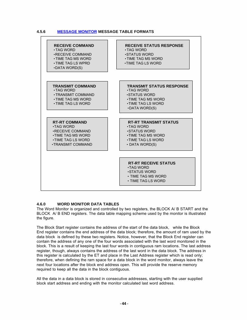
- -44
4.5.6 MESSAGE MONITOR MESSAGE TABLE FORMATS
RECEIVE COMMAND RECEIVE STATUS RESPONSE •TAG WORD •TAG WORD •RECEIVE COMMAND •STATUS WORD •TIME TAG MS WORD •TIME TAG MS WORD •TIME TAG LS WPRD •TIME TAG LS WORD •DATA WORD(S)
TRANSMIT COMMAND TRANSMIT STATUS RESPONSE •TAG WORD •TAG WORD •TRANSMIT COMMAND •STATUS WORD •TIME TAG MS WORD •TIME TAG MS WORD •TIME TAG LS WORD •TIME TAG LS WORD •DATA WORD(S)
RT-RT COMMAND RT-RT TRANSMIT STATUS •TAG WORD •TAG WORD •RECEIVE COMMAND •STATUS WORD •TIME TAG MS WORD •TIME TAG MS WORD •TIME TAG LS WORD •TIME TAG LS WORD •TRANSMIT COMMAND • DATA WORD(S)
RT-RT RECEIVE STATUS •TAG WORD •STATUS WORD • TIME TAG MS WORD • TIME TAG LS WORD
4.6.0 WORD MONITOR DATA TABLESThe Word Monitor is organized and controlled by two registers, the BLOCK A/ B START and theBLOCK A/ B END registers. The data table mapping scheme used by the monitor is illustratedthe figure.
The Block Start register contains the address of the start of the data block, while the BlockEnd register contains the end address of the data block; therefore, the amount of ram used by thedata block is defined by these two registers. Notice, however, that the Block End register cancontain the address of any one of the four words associated with the last word monitored in theblock. This is a result of keeping the last four words in contiguous ram locations. The last addressregister, though, always contains the address of the last word in the data block. The address inthis register is calculated by the ET and place in the Last Address register which is read only;therefore, when defining the ram space for a data block in the word monitor, always leave thenext four locations after the block end address open. This will provide the reserve memoryrequired to keep all the data in the block contiguous.
All the data in a data block is stored in consecutive addresses, starting with the user suppliedblock start address and ending with the monitor calculated last word address.
- -45
WORD MONITOR MEMORY ORGANIZATION
BLOCK A/B START ADDRESS DATA BLOCK
REGISTER
BLOCK A/B END ADDRESS
REGISTER
LAST ADDRESS A/B
REGISTER
4.6.1 WORD MONITOR TAG WORDThe WORD MONITOR TAG WORD contains information which is specific to the current wordtaken from the bus and stored in the data table. The ET loads these bits as the word isprocessed.
The TAG WORD is optional and it can be suppressed from the message table. See theConfiguration register 3 for details.
15 14 13 12 11 10 9 8GAP07 GAP06 GAP05 GAP04 GAP03 GAP02 GAP01 GAP00
7 6 5 4 3 2 1 0BUS OVRLAP 0 0 BCST SYNC ERROR GAPDET
Note: Reserved bits 5 and 4 always read 0
GAP Bits: 15: 8This field contains the time interval in microseconds between the current word received and thepreceding word received. The resolution of the time interval is 0.5us. If the gap is greater than orequal to 127.5us, then this field will hold at 127.5us. This field is valid only if bit 0 is a "1".
BUS Bits: 70= Word was received on bus "A".1= Word was received on bus "B".
BLOCK STARTADDRESS
TAG WORD
COMMAND/STATUS/DATA
TIME TAG MS WORD
TIME TAG LS WORD
BLOCK ENDADDRESS
TAG WORD
COMMAND/STATUS/DATA
TIME TAG MS WORD
TIME TAG LS WORDLAST WORDADDRESS
- -46
OVRLAP Bits: 61= A message was detected simultaneously on both busses . The Bus Monitor switches to the most current bus.
BCST Bits: 30 = Broadcast address NOT detected in the received word.1= Broadcast address WAS detected in the received word.
SYNC Bits: 20= The received word contained a Data sync.1= The received word contained a Command sync.
ERROR Bits: 10= Bus word had no errors.1= Bus word contained errors - encoding, parity, bit count, etc.
GAPDET Bits: 00= This word was contiguous with the previous bus word. Ignore bits (15 - 8).1= There was a gap between this word and the previous bus word. The gap time is recorded in bits (15 - 8).
4.6.2 WORD MONITOR COMMAND / STATUS - DATAThis is the word read from the bus.
4.6.3 WORD MONITOR TIME TAG MS WORDThis word contains the upper 16 bits of the 32 bit Time Tag.
4.6.4 WORD MONITOR TIME TAG LS WORDThis word contains the lower 16 bits of the 32 bit Time Tag.Note: Time Tag is optional. See Configuration register 3 for details.
5.0.0 REMOTE TERMINAL MODE CODE OPERATION
5.1.0 GENERALThis section defines the operation of the NHi- ET when operating as an RT during reception of allthe mode commands. The following terms are used in this section:
VALID COMMANDA command meeting the criteria established by the 1553B standard in paragraph 4.4.1.1.
INVALID COMMANDA command NOT meeting the criteria established by the 1553B standard in paragraph 4.4.1.1.
UNIMPLEMENTED COMMANDA command not implemented by the NHi- ET.
UNDEFINED MODE COMMANDThese commands are ignored by the NHi- ET.
- -47
The following general response characteristics apply to the NHi- ET when operating on thebus:
RECEIPT OF AN INVALID COMMAND There is no response and the command is ignored. RECEIPT OF AN UNIMPLEMENTED COMMAND There is no response and the command is ignored. RECEIPT OF AN UNDEFINED COMMAND There is no response and the command is ignored.
The following abbreviations are used in this discussion:
LSW = LAST STATUS WORD CDR = CONDITION REGISTER TW = TAG WORD IN DATA TABLE ME = MESSAGE ERROR BIT BCR = BROADCAST BIT
Additional information about each mode code is available in the Interrupt Vector register and theAuxilliary Vector register if it is set to be interrupt driven (see Data Table Pointer word, InterruptVector register and Auxiliary Vector register).
5.2.0 TABLE OF RT MODE CODE RESPONSES
5.2.1 DYNAMIC BUS CONTROL (00000; T/ R= 1)Responds with status except if broadcastBits set: *MDCD to "0" in CDR
COMMAND+ DATA WORDNo status responseBits set: *MDCD to "0" in CDR. ME to "1" in LSWINV to "1" in TW
T/ R= 0UNIMPLEMENTED COMMAND
BROADCASTUNIMPLEMENTED COMMAND
5.2.2 SYNCHRONIZE WITHOUT DATA (00001; T/ R= 1)VALID COMMANDResponds with status except if broadcastBits set: *MDCD to "0" in CDRIf broadcast- BCR, BCST in LSW & TW to "1"
COMMAND+ DATA WORDNo status responseBits set: *MDCD to "0" in CDR. ME to "1" in LSWINV to "1" in TW
T/ R= 0UNIMPLEMENTED COMMAND
T/ R= 0 AND BROADCASTUNIMPLEMENTED COMMAND
- -48
5.2.3 TRANSMIT LAST STATUS WORD (00010; T/ R= 1)VALID COMMANDResponds with last status except if broadcast. Status NOT updated.Bits set: *MDCD to "0" in CDR.
COMMAND+ DATA WORDStatus not cleared. No status response.Bits set: *MDCD to "0" in CDR. INV to "1" in TW.ME to "1" in LSW.
T/ R= 0UNIMPLEMENTED COMMAND
T/ R= 0 AND BROADCASTUNIMPLEMENTED COMMAND
5.2.4 INITIATE SELF TEST (00011; T/ R= 1)VALID COMMANDResponds with status except if broadcast.Bits set: *MDCD to "0" in CDR.If broadcast- BCR, BCST in LSW & TW to "1".
COMMAND+ DATA WORDNo status response.Bits set: *MDCD to "0" in CDR. ME to "1" in LSW.INV to "1" in TW.
T/ R= 0UNIMPLEMENTED COMMAND
T/ R= 0 AND BROADCASTUNIMPLEMENTED COMMAND
5.2.5 TRANSMITTER SHUTDOWN (00100; T/ R= 1)VALID COMMANDResponds with status except if broadcast. Transmitter on alternate bus inhibited.Alternate bus transmitter re- enabled by: Reset mode code, Override Transmitter Shutdown modecode, resetting RT, or power up. Bits set: *MDCD to "0" and alt bus (A) (B) XEN to "0" in CDR.If broadcast- BCR, BCST in LSW & TW to "1".
COMMAND+ DATA WORDNo status response.Bits set: *MDCD to "0" in CDR. ME to "1" in LSW.INV to "1" in TW.
T/ R= 0UNIMPLEMENTED COMMAND
T/ R= 0 AND BROADCASTUNIMPLEMENTED COMMAND
- -49
5.2.6 OVERRIDE TRANSMITTER SHUTDOWN (00101; T/ R= 1)VALID COMMANDResponds with status except if broadcast. Transmitter on alternate bus enabled.Bits set: *MDCD to "0" and alt bus (A) (B) XEN to "1" in CDR.If broadcast- BCR, BCST in LSW & TW to "1".
COMMAND+ DATA WORDNo status response.Bits set: *MDCD to "0" in CDR. ME to "1" in LSW.INV to "1" in TW.
T/ R= 0UNIMPLEMENTED COMMAND
T/ R= 0 AND BROADCASTUNIMPLEMENTED COMMAND
5.2.7 INHIBIT TERMINAL FLAG (00110; T/ R= 1)VALID COMMANDResponds with status except if broadcast.Bits set: *MDCD to "0" and TFE to "0" in CDR. Terminal Flag inhibited in LSW.
If broadcast- BCR, BCST in LSW & TW to "1".
COMMAND+ DATA WORDNo status response.Bits set: *MDCD to "0" in CDR. ME to "1" in LSW.INV to "1" in TW.
T/ R= 0UNIMPLEMENTED COMMAND
T/ R= 0 AND BROADCASTUNIMPLEMENTED COMMAND
5.2.8 OVERRIDE INHIBIT TERMINAL FLAG (00111; T/ R= 1)VALID COMMANDResponds with status except if broadcast.Bits set: *MDCD to "0" and TFE to "1" in CDR. Terminal Flag enabled in LSW.If broadcast- BCR, BCST in LSW & TW to "1".
COMMAND+ DATA WORDNo status response.Bits set: *MDCD to "0" in CDR. ME to "1" in LSW.INV to "1" in TW.
T/ R= 0UNIMPLEMENTED COMMAND
T/ R= 0 AND BROADCASTUNIMPLEMENTED COMMAND
- -50
5.2.9 RESET REMOTE TERMINAL (01000; T/ R= 1)VALID COMMANDResponds with status except if broadcast. Both Transmitters enabled and TerminalFlag enabled. Pointer base address register set to 2048 dec. External terminal address loaded.Bits set: BUSY to “1” in LSW after Status word transmission.If broadcast- BCR, BCST in LSW & TW set to "1".
COMMAND+ DATA WORDNo status response.Bits set:INV to "1" in TW.
T/ R= 0UNIMPLEMENTED COMMAND
T/ R= 0 AND BROADCASTUNIMPLEMENTED COMMAND
5.2.10 RESERVED MODE CODES (01001- 01111; T/ R= 1)VALID COMMANDResponds with status except if broadcast.Bits set: *MDCD to "0" in CDR.If broadcast- BCR, BCST in LSW & TW to "1".
COMMAND+ DATA WORDNo status response.Bits set: *MDCD to "0" in CDR. ME to "1" in LSW.INV to "1" in TW.
BROADCAST COMMAND+ DATA WORDNo status response.Bits set: *MDCD to "0" in CDR. ME and BCR set to "1" in LSW.INV and BCST set to "1" in TW.
T/ R= 0UNIMPLEMENTED COMMAND
T/ R= 0 AND BROADCASTUNIMPLEMENTED COMMAND
5.2.11 TRANSMIT VECTOR WORD (10000; T/ R= 1)VALID COMMANDResponds with status followed by vector word except if broadcast.Bits set: *MDCD to "0" in CDR.
COMMAND+ DATA WORDNo status response.Bits set: *MDCD to "0" in CDR. ME to "1" in LSW.INV to "1" in TW.
BROADCAST COMMANDUNIMPLEMENTED COMMAND
BROADCAST COMMAND+ DATA WORD
- -51
UNIMPLEMENTED COMMAND
T/ R= 0UNIMPLEMENTED COMMAND
T/ R= 0 AND BROADCASTUNIMPLEMENTED COMMAND
5.2.12 SYNCHRONIZE WITH DATA WORD (10001; T/ R= 0)VALID COMMANDResponds with status except if broadcast. Data word stored into RAM. Data word will updatelower 16 bits of real time clock depending on the configuration of the RTC CONTROLREGISTER.
Bits set: *MDCD to "0" in CDR.If broadcast- BCR, BCST in LSW & TW to "1".
COMMAND NO DATA WORDNo status response.Bits set: *MDCD to "0" in CDR. ME to "1" in LSW.
COMMAND + EXTRA DATA WORDNo status response.Bits set: *MDCD to "0" in CDR. ME to "1" in LSW.INV set to "1" in TW.
BROADCAST + EXTRA DATA WORDNo status response.Bits set: *MDCD to "0" in CDR. ME and BCR to "1" in LSW.INV and BCST to "1" in TW.
T/ R= 1UNIMPLEMENTED COMMAND
T/ R= 1 AND BROADCASTUNIMPLEMENTED COMMAND
5.2.13 TRANSMIT LAST COMMAND (10010; T/ R= 1)VALID COMMANDResponds with status followed by LAST VALID COMMAND word except if broadcast.Status and command registers NOT updated.Bits set: *MDCD to "0" in CDR.
COMMAND+ DATA WORDNo status response.Bits set: *MDCD to "0" in CDR.INV to "1" in TW.ME to "1" in LSW.
BROADCAST COMMANDUNIMPLEMENTED COMMAND
BROADCAST COMMAND+ DATA WORD
- -52
UNIMPLEMENTED COMMAND
T/ R= 0UNIMPLEMENTED COMMAND
T/ R= 0 AND BROADCASTUNIMPLEMENTED COMMAND
5.2.14 TRANSMIT BIT WORD (10011; T/ R= 1)VALID COMMANDResponds with status followed by BIT word.Bits set: *MDCD to "0" in CDR.
COMMAND+ DATA WORDNo status response.Bits set: *MDCD to "0" in CDR. ME to "1" in LSW.INV to "1" in TW.
BROADCAST COMMANDUNIMPLEMENTED COMMAND
BROADCAST COMMAND+ DATA WORDUNIMPLEMENTED COMMAND
T/ R= 0UNIMPLEMENTED COMMAND
T/ R= 0 AND BROADCASTUNIMPLEMENTED COMMAND
5.2.15 SELECTED TRANSMITTER SHUTDOWN (10100; T/ R= 0)VALID COMMANDResponds with status except if broadcast.Bits set:If broadcast- BCR, BCST to "1" in TW & LSW.
COMMAND + EXTRA DATA WORDNo responseBits set:
INV to "1" in TW.
COMMAND WITHOUT DATA WORDNo responseBits set:
BROADCAST WITH EXTRA DATA WORDNo responseBits set:INV & BCST to "1" in TW
BROADCAST WITHOUT DATA WORDNo responseBits set:5.2.16 OVERRIDE SELECTED TRANSMITTER SHUTDOWN (10101; T/ R= 0)
- -53
VALID COMMANDResponds with status except if broadcast.Bits set:If broadcast- BCR, BCST to "1" in TW & LSW.
COMMAND + EXTRA DATA WORDNo responseBits set:INV to "1" in TW.
COMMAND WITHOUT DATA WORDNo responseBits set:
BROADCAST WITH EXTRA DATA WORDNo responseBits set:INV & BCST to "1" in TW
BROADCAST WITHOUT DATA WORDNo responseBits set:
5.2.17 RESERVED MODE CODES (10110- 11111; T/ R= 1)VALID COMMANDResponds with status and data word.Bits set: *MDCD to "0" in CDR.
COMMAND + DATA WORDNo responseBits set: *MDCD to "0" in CDR. ME to "1" in LSW.INV to "1" in TW.
BROADCAST COMMANDUNIMPLEMENTED COMMAND
BROADCAST COMMAND+ DATA WORDUNIMPLEMENTED COMMAND
5.2.18 RESERVED MODE CODES (10110- 11111; T/ R= 0)VALID COMMANDResponds with status except if broadcast.Bits set:If broadcast- BCR, BCST to "1" in TW & LSW.
COMMAND + EXTRA DATA WORDNo responseBits set:INV to "1" in TW.
COMMAND WITHOUT DATA WORDNo responseBits set:BROADCAST WITH EXTRA DATA WORD
- -54
No responseBits set:INV & BCST to "1" in TW
BROADCAST WITHOUT DATA WORDNo responseBits set:
6.0.0 INITIALIZATIONThere are several types of initialization that can set up the NHi- ET parameters.
6.1.0 INTERNAL INITIALIZATIONThere are two methods of initializing the NHi ET. Each will produce the same results. They are:Hardware( MRST) and Software (writing to address 15, data not used). After these resets havebeen performed, the NHi ET is set to the RT mode and all internal state machines are reset.
The hardwire terminal address is loaded when a hardware or software reset occurs. The hardwireaddress is connected to I/ O DAT( 5: 0) pins. I/ O DAT( 4: 0) are used for the address and I/ ODAT5 is used to set odd parity in the address. The address is wired using external 4.7K pull-down resistors to set a low and internal 64K pull- up resistors to set a high.
The following table summarizes the condition of internal registers after a reset has beenperformed.Note: All register bit set to 0 at reset except as noted.
REGISTER RESET TABLEADDR REGISTER BITS=1 COMMENTS
0 CONTROL HWD1 POINTER TABLE ADDRESS LOADED WITH 4096 DEC WORD2 BASIC STATUS* HARDWIRE ADDRESS LOADED
21 CONFIGURATION 33 INTERRUPT MASK ALL ALL INTERRUPTS ARE MASKED4 INTERRUPT VECTOR3 INTERRUPT REQUEST4 AUXILLIARY VECTOR UNDEFINED
5,6 RTC; HIGH.LOW NOT AFFECTED BY RESET7 RTC CONTROL8 FIFO RESET ONLY BY MRST
11 LAST COMMAND UNDEFINED12 LAST STATUS* HARDWARE ADDRESS LOADED18 ENCODER STATUS19 CONDITION 9,11-1313 FRAME “A” POINTER LOADED WITH 2058 DEC16 FRAME “B” POINTER LOADED WITH 4096 DEC14 FRAME "A" LENGTH CLEARED17 FRAME "B" LENGTH CLEARED
MSG MONITOR ADDR FILTER 1 ALL ADDRESSES UNMASKEDMSG MONITOR ADDR FILTER 2 ALL ADDRESSES UNMASKED
* See RESET BUSY TABLE
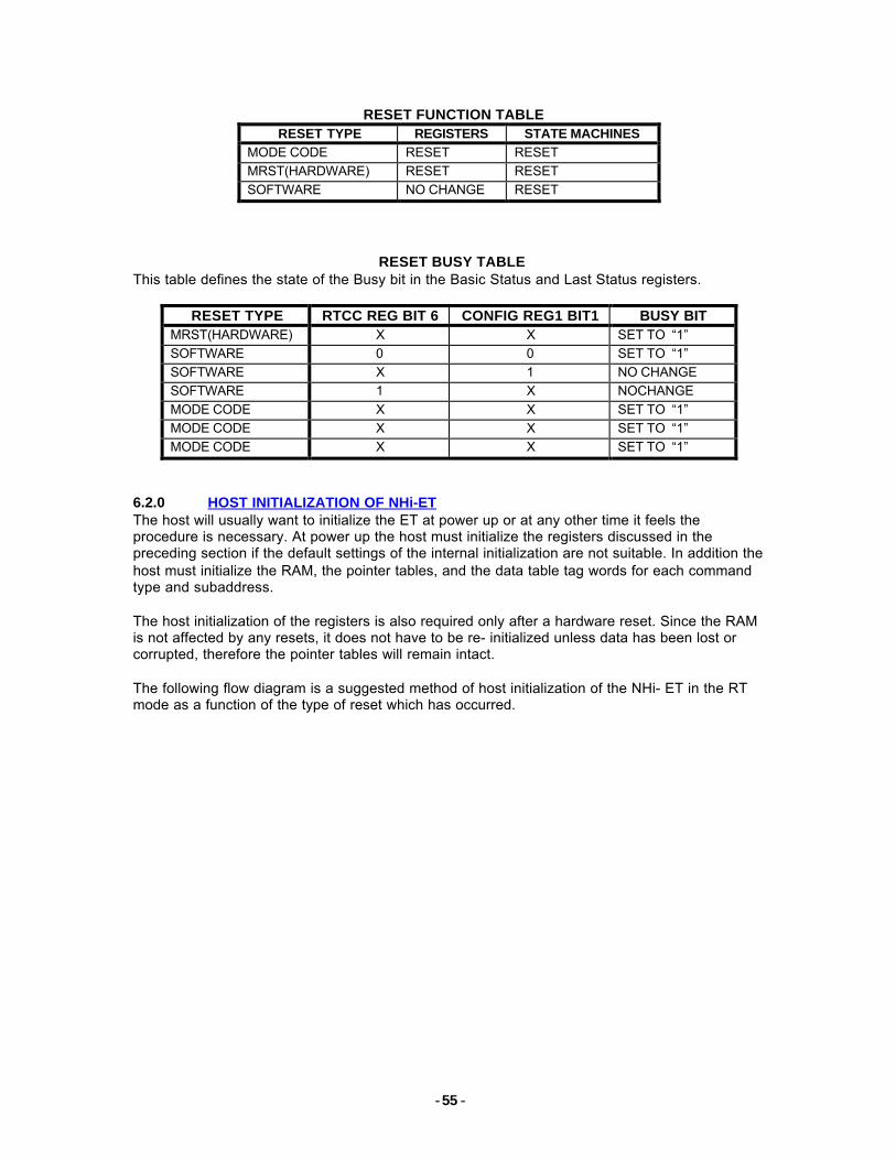
- -55
RESET FUNCTION TABLERESET TYPE REGISTERS STATE MACHINES
MODE CODE RESET RESETMRST(HARDWARE) RESET RESETSOFTWARE NO CHANGE RESET
RESET BUSY TABLEThis table defines the state of the Busy bit in the Basic Status and Last Status registers.
RESET TYPE RTCC REG BIT 6 CONFIG REG1 BIT1 BUSY BITMRST(HARDWARE) X X SET TO “1”SOFTWARE 0 0 SET TO “1”SOFTWARE X 1 NO CHANGESOFTWARE 1 X NOCHANGEMODE CODE X X SET TO “1”MODE CODE X X SET TO “1”MODE CODE X X SET TO “1”
6.2.0 HOST INITIALIZATION OF NHi-ETThe host will usually want to initialize the ET at power up or at any other time it feels theprocedure is necessary. At power up the host must initialize the registers discussed in thepreceding section if the default settings of the internal initialization are not suitable. In addition thehost must initialize the RAM, the pointer tables, and the data table tag words for each commandtype and subaddress.
The host initialization of the registers is also required only after a hardware reset. Since the RAMis not affected by any resets, it does not have to be re- initialized unless data has been lost orcorrupted, therefore the pointer tables will remain intact.
The following flow diagram is a suggested method of host initialization of the NHi- ET in the RTmode as a function of the type of reset which has occurred.
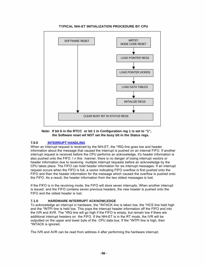
- -56
TYPICAL NHi-ET INITIALIZATION PROCEDURE BY CPU
Note: If bit 6 in the RTCC or bit 1 in Configuration reg 1 is set to “1”, the Software reset wil NOT set the busy bit in the Status regs.
7.0.0 INTERRUPT HANDLINGWhen an interrupt request is received by the NHi-ET, the *IRQ line goes low and headerinformation about the message that caused the interrupt is pushed on an internal FIFO. If anotherinterrupt request is received before the CPU performs an acknowledge, it's header information isalso pushed onto the FIFO. I n this manner, there is no danger of losing interrupt vectors orheader information due to receiving multiple interrupt requests before an acknowledge by theCPU takes place. The FIFO can hold header information for six interrupt messages. If an interruptrequest occurs when the FIFO is full, a vector indicating FIFO overflow is first pushed onto theFIFO and then the header information for the message which caused the overflow is pushed ontothe FIFO. As a result, the header information from the two oldest messages is lost.
If the FIFO is in the revolving mode, the FIFO will store seven interrupts. When another interruptis issued and the FIFO contains seven previous headers, the new header is pushed onto theFIFO and the oldest header is lost.
7.1.0 HARDWARE INTERRUPT ACKNOWLEDGETo acknowledge an interrupt in hardware, the *INTACK line is taken low, the *HCS line held highand the *INTPI line is held low. This pops the interrupt header information off the FIFO and intothe IVR and AVR. The *IRQ line will go high if the FIFO is empty, but remain low if there areadditional interrupt headers on the FIFO. If the NHi-ET is in the RT mode, the IVR will beoutputted on the upper and lower byte of the CPU data bus. If the *INTPI line is high, then*INTACK is ignored.
The IVR and AVR can be read from address 4 after performing the hardware interrupt.
MRTST/MODE CODE RESET
LOAD POINTER REGS
LOAD POINTER WORDS
LOAD DATA TABLES
INITIALIZE REGS
CLEAR BUSY BIT IN STATUS REGS
SOFTWARE RESET
- -57
If there are more interrupt headers on the FIFO, indicated by the *IRQ remaining low after theinterrupt acknowledge, the procedure is repeated until the FIFO is empty. An empty FIFO isindicated by the *IRQ line returning high after an interrupt acknowledge and bit 8 in the AVR willbe a "1".
7.2.0 SOFTWARE INTERRUPT ACKNOWLEDGEIf the host CPU does not support a hardware interrupt acknowledge, a software acknowledge canbe performed by reading address 8. This read pops the interrupt header information off the FIFOand into the IVR and AVR and places their contents on the CPU data bus. The *IRQ line will gohigh if the FIFO is empty and remain low if there are additional interrupt headers on the FIFO.
If there are more interrupt headers on the FIFO, indicated by the *IRQ remaining low after theinterrupt acknowledge, the procedure is repeated until the FIFO is empty. An empty FIFO isindicated by the *IRQ line returning high after an interrupt acknowledge and the MSB in the AVRwill be a "1".
8.0.0 TIPS - HINTS 'N TRICKSThis section will help the USER apply the ET to a system and implement its various features.
8.1.0 BUS CONTROLLER APPLICATIONSThe NHi-ET Bus Controller is flexible, powerful, and very easy to use. The number of operationsrequired to initialize the device and to examine results of a data message transfer has beenminimized.
The BC function of the NHi-ET employs registers embedded in the protocol chip and its internalram to perform its various tasks. These tasks include:
Initiating Message Transfers Diagnose RT Responses Take Appropriate Action on Error Conditions Data StorageMessage lists, containing the addresses of specific messages, are used to develop specificoperational scenarios. The number of message lists and message tables is limited only by thesize of the ram. A list can have up to 1024 messages. A message list is activated by placing itsaddress in one of the two FRAME START REGISTERS and the list length in one of the FRAMELENGTH REGISTERS.
8.1.1 BC REGISTERSThis a brief description of the BC registers and their role. Specific bit functions are given in theaddress map section of this manual. Only the functions pertinent to the BC are described here.The following registers are used in the BC function:
8.1.1.1 CONFIGURATION REG 2 Address: 4Complete EOM and continue.Goto next message.Goto EOF and continue.Stop at end of current message.Stop at end of current frame.Abort - Go off line.Go default frame.Note: The first three Functions only apply to a bus jam condition.
- -58
8.1.1.2 CONFIGURATION REG 1 Address: 9Mode select - RT, BC, MT.Start BC.Select default frame A or B.Select default bus A or B.Force bus A or B.
8.1.1.3 FRAME “A” POINTER Address: 13Holds address of a selected BC message list.
8.1.1.4 FRAME “A” LENGTH Address: 14Holds number of messages in frame A message list.End of frame A options - Stop, Repeat , Go Alternate.Stop on frame error.Stop on status set.Interrupt at end of frame.
8.1.1.5 FRAME “B” POINTER Address: 16Holds address of a selected BC message list
8.1.1.6 FRAME “B” LENGTH Address: 17Holds number of messages in frame B message list.End of frame B options - Stop, Repeat, Go Alternate.Stop on frame error.Stop on status set.Interrupt at end of frame.
8.1.1.7 CONDITION REGISTER Address 19Bus A jammed.Bus B jammed.Current BC frame A or B.End of frame A.End of frame B.Current frame busy.8.1.1.8 END OF FRAME GAP Address: 20End of frame delay before start of next frame - 64us resolution, 16 bits.
8.1.1.9 CONFIGURATION REG 3 Address: 21Sets bus jam threshold - the number of extra words( 0- 31) a message can have before abus jam is declared.Defines response to BCST bit if set in status word.Sets global retry options.
8.1.2 BC RAMThe BC ram is used to store message lists and message tables. A message list is a block ofconsecutive memory locations, each of which contains the address of a message table. This listcan contain any number of message table addresses up to a maximum of 1024. Many messagelists can be stored in the ram, limited only by ram size, each one containing a different scenario.A particular message table may be a member of any number of message lists and occupy thesame or different positions in each list.
- -59
8.1.3 BC MESSAGE TABLEA message table is a block of consecutive memory which contains all the components of onemessage. These components are:BC Control word.BC Command word.Message gap word.32 bit time tag( two words).2nd Command word (RT- RT only).Data words.Status word.2nd Status word( RT- RT only).
In the case of an RT- RT transfer, the second command and status words are also in themessage block as shown. The message block is designed to contain all the informationassociated with the message. Parts of the message, the command word for example, are notsegregated into a separate ram area which would complicate reading or writing a message blockby the CPU. The unified message block approach used in the NHi- ET provides faster access to amessage block by the CPU and minimizes overhead.
8.1.4 BC CONTROL WORDThe BC control word is used by the CPU to define parameters in the message and it is used bythe Protocol chip to report information back to the CPU. The following parameters are loaded intothe BC control word by the CPU and used by the protocol chip for a message:Status bit analysis.Message bus - A or B.Local retry actio in the event of an error. If there is no local retry, then the global retry action set inconfiguration register 2 is used if an error occurs.The following information about that message is loaded into the BC control word by the protocolchip and used by the CPU:Start of message flag.No response.Error.Status bit set.Retry attempted.End of message flag.
8.1.5 BC COMMAND WORDThe command word is any of the 1553 valid commands. This word defines the type of datatransfer in the message BC to RT, RT to BC, RT to RT, or Mode code.
8.1.6 MESSAGE GAP WORDThe message gap word defines delay between the end of the current message and the start ofthe next message in the list. The maximum intermessage gap is 4ms with a resolution 1us. Theminimum inter message gap is approximately 8us when the delay is set to 0. The following otherparameters are set in the message gap word:Message stop on error.Message stop on status set.Interrupt on end of message.NO- OP.
If the NO- OP is set in a message, the message is ignored except for its inter message delay.This feature can be used to extend the maximum intermessage gap from 4ms to any length, justby putting a series of NO- OP messages between two operational messages.
- -60
8.1.7 32 BIT TIME TAG( 2 WORDS)The internal time tag resolution is selectable as 1,2,4,8,16,32 or 64us.
8.1.8 BC INTERRUPTSThe following conditions will cause an interrupt to the CPU if they are not masked by the interruptmask register.
PRIORITY INTERRUPT COMMENT0 END OF MESSAGE ENABLED IN MSG GAP WORD1 END OF FRAME ENABLED IN REGS 14 & 172 ERROR ERRORS IN RT RESPONSE3 RETRY ERROR CAUSED RETRY4 FIFO OVERFLOW FIFO IS FULL5 STATUS SET STATUS BIT SET OR STATUS ADDRESS
ERROR6 NO RESPONSE RT DID NOT RESPOND7 FAILSAFE TIMEOUT FAILSAFE TIMEOUT IN NHi-ET ENCODER
The following header information about the BC message that caused the interrupt is pushed on tothe Fifo:
PriorityMessage number in frameFrame A or BBus A or B
8.1.9 BUS CONTROLLER EXAMPLENow, lets see how we would put the BC into operation!
The following sequence is one approach:
Define various message tables and load them into ram.Define various message lists and load them withn the addresses of the previously definedmessage tables.
At this point, we have the ram loaded with individual messages tables and a number of messagelists. Each message list contains the addresses of several( up to 1024) message tables.
Load the address of the first message list to be used into register 13, Frame A.Load the total number of messages in that list into register 14, Frame length A.Load the address of the second message list to be used into register 16, Frame B.Load the total number of messages in that list into register 17, Frame length B.Set the mode to BC in register 9.Set the default frame to A in register 9.Set the "Default bus" in register 9.Set "Go alternate frame" in register 14.Set "int on EOF" in register 14.Set "Stop at EOF" in register 17.Set "int on EOF" in register 17.Set "Start BC" in register 9.
- -61
Based on these setup conditions, the following events will occur:
Frame A will execute the message list it contains. At the end of frame A, a frame gap delay willoccur if a number other than 0 was loaded into register 20. At the end of the frame gap delay, Thealternate frame, in this case B, will execute the message list it contains. At the end of frame B, thesequence will end and the BC will go off line.
Note: The alternate frame is the frame which is NOT the current frame. If the current frame is B,then the alternate frame is A. The alternate bus is the bus which is NOT the active bus.
This method is applicable if each message list contains many messages, tens or hundreds;however, each message list may only contain 10 or 20 messages and we would like to run anumber of the small message lists automatically.
For the case of running many small message lists automatically, the approach is slightly different.
Lets say we want to run 10 different message lists automatically.
First create a super message list which contains all the addresses of the 10 smaller sub messagelists. If we want to know when each of the sublists is completed, set the last message in each sublist to fire the interrupt. If we want to examine some of the data before the next sub list begins,set the inter message gap on the last message of the sub list to what ever delay is required.Then:Load the address of the super message list into register 13, Frame A.Load the total number of messages in the super list into register 14, Frame length A.Set the mode to BC in register 9.Set the default frame to A in register 9.Set the "Default bus" in register 9.Set "int on EOF" in register 14.Set "Stop at EOF" in register 14.Set "Start BC" in register 9.All the messages in the super list will be executed and an interrupt will be issued at the end ofeach sub list. An intermessage gap of some defined value will separate each sub list ofmessages.
Instead of stopping at the end of frame A, we could have elected to "Go alternate frame", in whichcase, frame B would then execute what ever message lists were in frame B. If we then selectedthe "Go alternate frame" option at the end of frame B, frame A would be executed.
Note: The default frame is the frame selected in configuration register 1. The default bus isthe bus selected in the BC control word.
8.1.10 SAMPLE BUS CONTROLLER MEMORY MAP
BC Registers
REGISTERS DATA(hex)CONFIGURATION 1 0900CONFIGURATION 2 0000CONFIGURATION 3 0003INTERRUPT MASK 0000FRAME A MSG TABLE ADDRESS 0100FRAME A LENGTH 0004
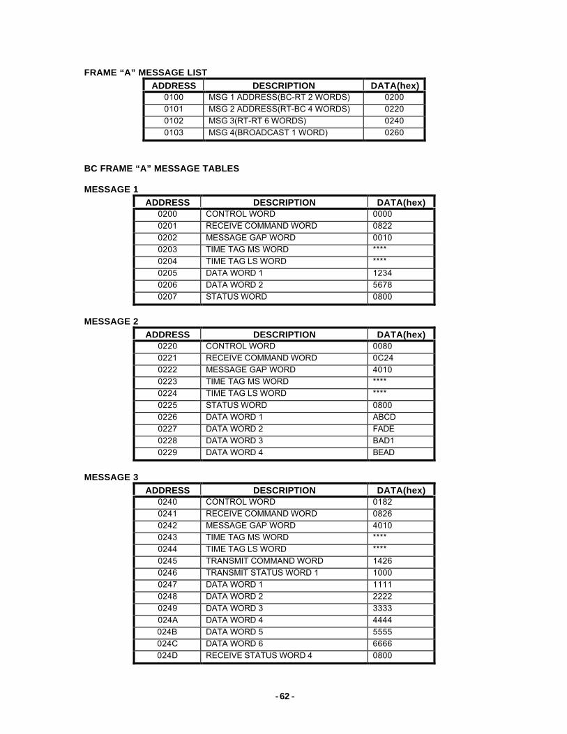
- -62
FRAME “A” MESSAGE LISTADDRESS DESCRIPTION DATA(hex)
0100 MSG 1 ADDRESS(BC-RT 2 WORDS) 02000101 MSG 2 ADDRESS(RT-BC 4 WORDS) 02200102 MSG 3(RT-RT 6 WORDS) 02400103 MSG 4(BROADCAST 1 WORD) 0260
BC FRAME “A” MESSAGE TABLES
MESSAGE 1ADDRESS DESCRIPTION DATA(hex)
0200 CONTROL WORD 00000201 RECEIVE COMMAND WORD 08220202 MESSAGE GAP WORD 00100203 TIME TAG MS WORD ****0204 TIME TAG LS WORD ****0205 DATA WORD 1 12340206 DATA WORD 2 56780207 STATUS WORD 0800
MESSAGE 2ADDRESS DESCRIPTION DATA(hex)
0220 CONTROL WORD 00800221 RECEIVE COMMAND WORD 0C240222 MESSAGE GAP WORD 40100223 TIME TAG MS WORD ****0224 TIME TAG LS WORD ****0225 STATUS WORD 08000226 DATA WORD 1 ABCD0227 DATA WORD 2 FADE0228 DATA WORD 3 BAD10229 DATA WORD 4 BEAD
MESSAGE 3ADDRESS DESCRIPTION DATA(hex)
0240 CONTROL WORD 01820241 RECEIVE COMMAND WORD 08260242 MESSAGE GAP WORD 40100243 TIME TAG MS WORD ****0244 TIME TAG LS WORD ****0245 TRANSMIT COMMAND WORD 14260246 TRANSMIT STATUS WORD 1 10000247 DATA WORD 1 11110248 DATA WORD 2 22220249 DATA WORD 3 3333024A DATA WORD 4 4444024B DATA WORD 5 5555024C DATA WORD 6 6666024D RECEIVE STATUS WORD 4 0800
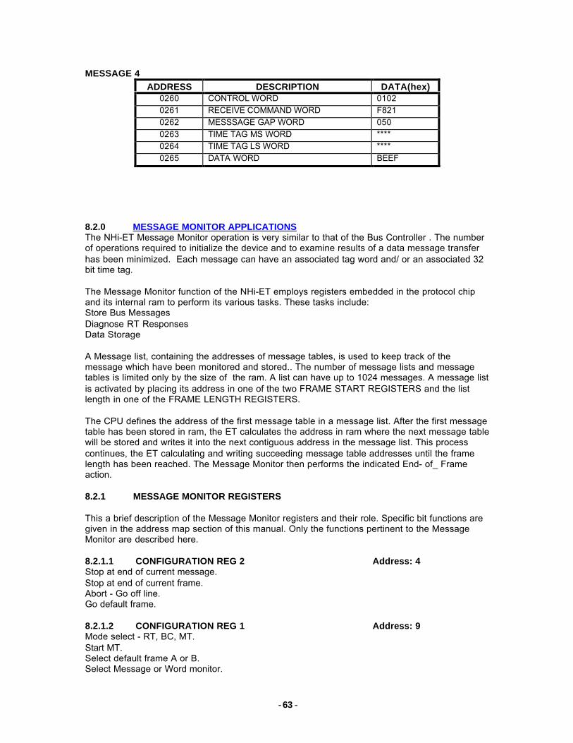
- -63
MESSAGE 4ADDRESS DESCRIPTION DATA(hex)
0260 CONTROL WORD 01020261 RECEIVE COMMAND WORD F8210262 MESSSAGE GAP WORD 0500263 TIME TAG MS WORD ****0264 TIME TAG LS WORD ****0265 DATA WORD BEEF
8.2.0 MESSAGE MONITOR APPLICATIONSThe NHi-ET Message Monitor operation is very similar to that of the Bus Controller . The numberof operations required to initialize the device and to examine results of a data message transferhas been minimized. Each message can have an associated tag word and/ or an associated 32bit time tag.
The Message Monitor function of the NHi-ET employs registers embedded in the protocol chipand its internal ram to perform its various tasks. These tasks include:Store Bus MessagesDiagnose RT ResponsesData Storage
A Message list, containing the addresses of message tables, is used to keep track of themessage which have been monitored and stored.. The number of message lists and messagetables is limited only by the size of the ram. A list can have up to 1024 messages. A message listis activated by placing its address in one of the two FRAME START REGISTERS and the listlength in one of the FRAME LENGTH REGISTERS.
The CPU defines the address of the first message table in a message list. After the first messagetable has been stored in ram, the ET calculates the address in ram where the next message tablewill be stored and writes it into the next contiguous address in the message list. This processcontinues, the ET calculating and writing succeeding message table addresses until the framelength has been reached. The Message Monitor then performs the indicated End- of_ Frameaction.
8.2.1 MESSAGE MONITOR REGISTERS
This a brief description of the Message Monitor registers and their role. Specific bit functions aregiven in the address map section of this manual. Only the functions pertinent to the MessageMonitor are described here.
8.2.1.1 CONFIGURATION REG 2 Address: 4Stop at end of current message.Stop at end of current frame.Abort - Go off line.Go default frame.
8.2.1.2 CONFIGURATION REG 1 Address: 9Mode select - RT, BC, MT.Start MT.Select default frame A or B.Select Message or Word monitor.
- -64
8.2.1.3 FRAME “A” POINTER Address: 13Holds address of a selected MT message list.
8.2.1.4 FRAME “A” LENGTH Address: 14Holds number of messages in frame A message list.End of frame A options - Stop, Repeat , Go Alternate.Interrupt at end of frame.
8.2.1.5 FRAME “B” POINTER Address: 16Holds address of a selected MT message list.
8.2.1.6 FRAME “B” LENGTH Address: 17Holds number of messages in frame B message list.End of frame B options - Stop, Repeat, Go Alternate.Interrupt at end of frame.
8.2.1.7 CONDITION REGISTER Address: 19Current BC frame A or B.End of frame A.End of frame B.Current frame busy.
8.2.1.8 CONFIGURATION REGISTER 3 Address: 21Enable tag word option.Enable time tag option.
8.2.1.9 ADDRESS FILTER (0- 15) Address: 22Masks terminal addresses 0 - 15.A "1" will mask the address.
8.2.1.10 ADDRESS FILTER (16- 31) Address: 26Masks terminal addresses 16 - 31.A "1" will mask the address.
8.2.2 MESSAGE MONITOR RAMThe Message Monitor ram is used to store message lists and message tables in much the samemanner as the BC. A message list is a block of consecutive memory locations, each of whichcontains the address of a message table. This list can contain any number of message tableaddresses up to a maximum of 1024. Many message lists can be stored in the ram, limited onlyby ram size, each one containing a different scenario.
8.2.3 MESSAGE MONITOR MESSAGE TABLEA message table is a block of consecutive memory which contains all the components of onemessage. These components include:Tag word control word.Command word or Status word.32 bit time tag( two words).Data words.
The format of a Message Table is a function of the type of command stored in ram. Theseformats are illustrated in a later section of this manual. The unified message block approachagain used in the Message monitor to provide faster access to a message block by the CPU andminimizes overhead.
- -65
8.2.4 MESSAGE MONITOR TAG WORDThe ET loads the Message monitor tag word with information about the message received. Thisinformation is used by the CPU to analyze the message. The following parameters are loadedinto the Monitor tag word by the ET:Start of message flag.Data error - Data word( s) contained error( s).Command 1 error - Comand word contained error( s).Command 2 error - Second command word of an RT- RT command contained error( s).Over lap - A message was detected on the alternate bus before the current message was Completed. The Message monitor aborts processing the current message, switches to the alternate bus and begins processing the new message.Sync error - A contiguous data word had a command sync.Bus A- B.RT- RTcommand - Message was an RT- RT command.End of message flag.
8.2.5 COMMAND WORD OR STATUS WORDThis is the Command or Status word associated with the message.
8.2.6 DATA WORD( S)These are the data word( s) associated with the message.
8.2.7 MESSAGE MONITOR EXAMPLESetting up and Implementing the MESSAGE monitor!
Put address of message list in FRAME REG.Put address of 1st message table in 1st location of message list.Put message list size in FRAME LENGTH REG.Set end of MESSAGE LIST options in FRAME LENGTH REG.Select end of MESSAGE LIST interrupt in FRAME LENGTH REG.Set the address Masks in REG's 22 and 26.Select tag word option in REG 21.Select time tag option in REG 21.Select MESSAGE monitor in REG 9.Start monitor in REG 9.
The monitor now collects messages until the message list size is reached. The selected End- of-Message List option is executed and an interrupt is issued if enabled.
The CPU can now read the entire message list. Each word in the message list is the address of adata block stored in ram. The first word in the block is the Tag Word associated with thatmessage.
8.3.0 WORD MONITOR APPLICATIONSThe NHi-ET Word Monitor operation collects data on a word- by- word basis . Each word that isreceived and stored in the ram can have an associated tag word and/ or an associated 32 bit timetagged The number of operations required to initialize the device and to examine results of a datamessage transfer has been minimized.
The Word Monitor function of the NHi-ET employs registers embedded in the protocol chip and itsinternal ram to perform its various tasks. These tasks include:Store Bus wordsDiagnose RT ResponsesData Storage
- -66
A data block, containing the bus word ,tag word and time tag, is used to store the monitoreddata.. The begining of the data block is determined by the address placed in the BLOCK STARTREGISTER and the end of the data block is determined by the address in the BLOCK ENDREGISTER.
The BLOCK END REGISTER works inconjunction with the LAST ADDRESS REGISTER. Since abus word can occupy up to four words in ram, tag word + 2 time tag words, the address in theBLOCK END REGISTER could occur on any of these four words. In order to keep the four wordsof the last ram entry contiguous in ram, the Word monitor uses the LAST ADDRESS REGISTERto store the address of the last word in the data block. The ET calculates this address and puts itin the LAST ADDRESS REGISTER. This address could be identical to that in the BLOCK ENDREGISTER or up to three addresses greater; therefore, always reserve the four addresses afterthe address in the BLOCK END REGISTER for this contingency.
8.3.1 WORD MONITOR REGISTERSThis a brief description of the Message Monitor registers and their role. Specific bit functions aregiven in the address map section of this manual. Only the functions pertinent to the MessageMonitor are described here.
CONFIGURATION REG 2 Address: 4Stop at end of current message.Stop at end of current frame.Abort - Go off line.Go default frame .
8.3.1.2 CONFIGURATION REG 1 Address: 9Mode select - RT, BC, MT.Start MT.Select default frame A or B.Select Message or Word monitor.
8.3.1.3 BLOCK “A” START Address: 13Holds address of a selected MT message list.
8.3.1.4 BLOCK “A” END Address: 14Holds number of messages in frame A message list.End of frame A options - Stop, Repeat , Go Alternate.Interrupt at end of frame.
8.3.1.5 BLOCK “B” START Address: 16Holds address of a selected MT message list.
8.3.1.6 BLOCK “B” END Address: 17Holds number of messages in frame B message list.End of frame B options - Stop, Repeat , Go Alternate.Interrupt at end of frame.
8.3.1.7 CONDITION REGISTER Address: 19Current BC frame A or B.End of frame A.End of frame B.Current frame busy.
- -67
8.3.1.8 WORD MONITOR END OF BLOCK OPTIONS Address: 20End of block A options - Stop, Repeat, Go Alternate.Interrupt at end of block A.End of block B options - Stop, Repeat, Go Alternate.Interrupt at end of block B.
8.3.1.9 CONFIGURATION REGISTER 3 Address: 21Enable tag word option.Enable time tag option.Enable time tag command syncs only option.
8.3.2 WORD MONITOR EXAMPLESetting up and Implementing the WORD monitor!
Set address of data block in BLOCK A/ B REG.Set end of data block address in BLOCK A/ B END REG.Set end of DATA BLOCK options in REG 20.Select end of block interrupt in REG 20.Select tag word option in REG 21.Select time tag option in REG 21.Select word monitor in REG 9.Start monitor in REG 9.
The monitor now collects data until the end of block address is reached. The address of the lastword in the block is stored in the Last Word Address register, the selected End- of- Block option isexecuted and an end of block interrupt is issued if enabled in reg 20.
The CPU can now read the entire data block and use the Tag Words and the Time Tags toanalyze the data.
8.4.0 SIMULTANEOUS MONITOR AND REMOTE TERMINALThe ET can operate as a simultaneous monitor and remote terminal. This mode is activated bysetting bits 8 and 9 of Configuration register 1 to a "1". In this mode the ET will respond as aremote terminal to the address set in the Basic Status register. This address is set either by thehardwire address or software.
The ET will respond to all addresses except that in the Basic Status register as a monitor, wordmonitor or message monitor depending on the monitor mode selected. In the message monitormode, the ET will only respond to terminal addresses which have not been masked in registers22 and 26.
When the ET receives a message with the address in the Basic Status register, it will become afully operational Remote Terminal for that message.
8.4.1 SIMULTANEOUS MODE INTERRUPT HANDLINGIn this dual mode of operation, all the interrupts for the Remote terminal and Monitor operationremain valid; therefore both RT and MT messages can set interrupts and push headers on theFIFO during the dual mode operation.
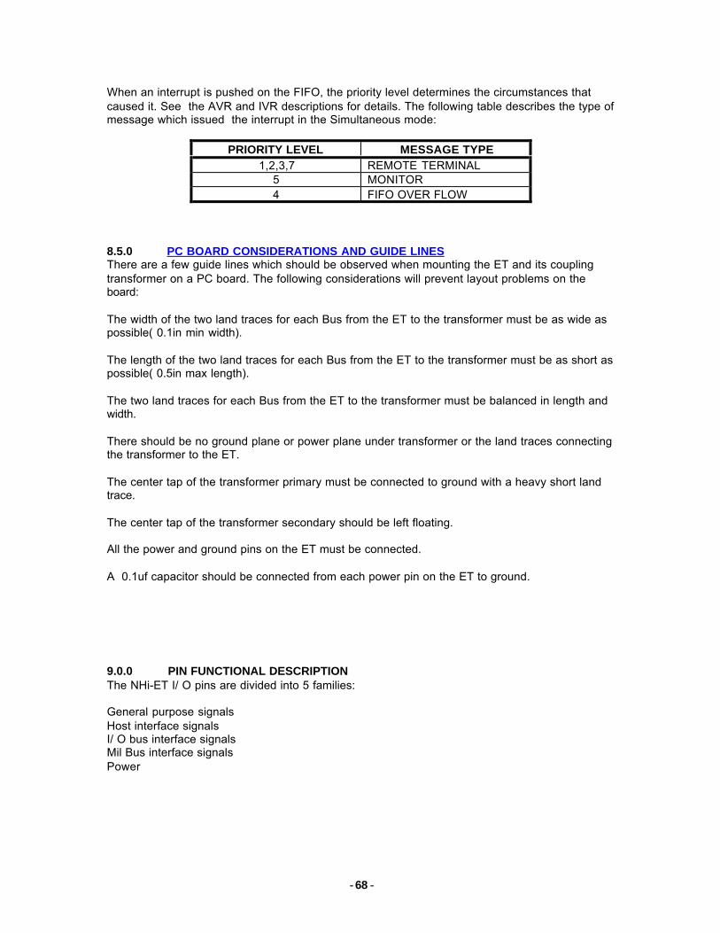
- -68
When an interrupt is pushed on the FIFO, the priority level determines the circumstances thatcaused it. See the AVR and IVR descriptions for details. The following table describes the type ofmessage which issued the interrupt in the Simultaneous mode:
PRIORITY LEVEL MESSAGE TYPE1,2,3,7 REMOTE TERMINAL
5 MONITOR4 FIFO OVER FLOW
8.5.0 PC BOARD CONSIDERATIONS AND GUIDE LINESThere are a few guide lines which should be observed when mounting the ET and its couplingtransformer on a PC board. The following considerations will prevent layout problems on theboard:
The width of the two land traces for each Bus from the ET to the transformer must be as wide aspossible( 0.1in min width).
The length of the two land traces for each Bus from the ET to the transformer must be as short aspossible( 0.5in max length).
The two land traces for each Bus from the ET to the transformer must be balanced in length andwidth.
There should be no ground plane or power plane under transformer or the land traces connectingthe transformer to the ET.
The center tap of the transformer primary must be connected to ground with a heavy short landtrace.
The center tap of the transformer secondary should be left floating.
All the power and ground pins on the ET must be connected.
A 0.1uf capacitor should be connected from each power pin on the ET to ground.
9.0.0 PIN FUNCTIONAL DESCRIPTIONThe NHi-ET I/ O pins are divided into 5 families:
General purpose signalsHost interface signalsI/ O bus interface signalsMil Bus interface signalsPower
- -69
9.1.0 GENERAL PURPOSE SIGNALS
MRST_ L Master Reset (active low, input). Initializes all registers and state machines. ET reads hardwire terminal address. Reset pulse width is 300ns min. The reset recovery time is 12us max after the rising edge of the reset pulse.
CLK_ H Terminal Clock from 10 Mhz oscillator (input).
9.2.0 HOST INTERFACE SIGNALS
H_ DAT (15: 0) Host Data bus (bi- directional).
H_ ADR (16/14: 1) Host Address bus (input).
HCS_ L Chip Select (active low, input). Selects the NHi-ET. The falling edge of HCS_ L is used to latch the host address and indicates the start of a host memory cycle. The rising edge terminates the current cycle. During a host read- modify- write cycle. This signal must remain active from the beginning to the end of an access cycle. NOTE: The host should not hold *HCS active for more than 5 microseconds, otherwise timing errors on the Mil-Std Data bus may occur.
HWRL_ L Host Write Lower Byte (active low, input).
HWRH_ L Host Write Upper Byte (active low, input).
HRD_ L Host Read (active low, input).
DACK_ L Host Data Transfer Acknowledge (active low, open drain output, 5K internal pull up). Indicates to the host that a data transfer has been completed. When the host reads data, it takes HCS_L low and the HRD_ L low. The ET will indicate that stable data is on the bus by outputting a low on DTACK_ L. When the Host writes data, it takes HCS_ L low and HWRL_ L and/ or HWRH_ L low. The ET then indicates that it has completed the write cycle by outputting a low on DTACK_ L.
IRQ_ L Host Interrupt Request (active low, open drain output, 5K internal pullup). The IRQ_L will remain low until the Fifo is empty
INTACK_ L Host Interrupt Acknowledge (active low, input). When HRD_ L= 0, INTACK_ L= 0, and HCS_ L= 1, an interrupt vector is popped from the FIFO, the IVR and AVR registers are updated, and the IVR is outputted onto both the lower and upper bytes of the host data bus, provided the INTPI_ L is low and the ET is in the RT mode.
INTPI_ L Interrupt Priority Input (active low, input). This signal is used to daisy chain interrupt requests on the host bus. This signal must be active for the ET to output an interrupt vector.
- -70
INTPO_L_DSC Interrupt Priority Output, Disconnect Signal (output). This pin has 2 possible functions, depending on the M1760 bit in the RTC CONTROL register. If M1760= 0, then the signal is used to daisy chain interrupt requests on the host bus. When the ET requests an interrupt, this signal is output high; otherwise, this signal is equal to INTPI_ L. If M1760= 1, then the pin is set to "1" when the store is disconnected (see EXTERNAL TERMINAL ADDRESS BUFFER for details).
9.3.0 DISCRETE I/O BUS INTERFACE SIGNALS
I/ O_ RD_ L I/ O Read (active low, output).
I/ O_ WR_ L I/ O Write (active low, output).
I/ O_ ADR (2: 1) I/ O Address (outputs).These three signals can be used to select 4 byte- wide input devices and 4 byte- wide outputdevices which reside on the I/ O Data bus.
I/ O_ DAT (7: 0) I/ O DATA bus (bi- directional). This bus is used for messages that are mapped to I/O, discreet pulse message identifiers and setting the Hardwire RT address.
CMDS Command Strobe (active high, output; 100ns). This strobe is used for two special I/ O operations. When the strobe is active during a write cycle (i. e., CMDS= 1, I/ O WR_ L= 0), valid commands or pulses appear on the I/ O bus (see the CMDO bit in CONTROL register for details). When the strobe is active during a read cycle (i. e., CMDS= 1, I/ O RD_ L= 0), the EXTERNAL TERMINAL ADDRESS buffer is accessed.
PLSCMD_ BUS_ JAM Pulse Command or Bus Jam (active high, output; 100ns). RT MODE: Depends on the value of the CMDO bit in the CONTROL register. If CMDO= 0, then a pulse is issued whenever a bus message accesses a data table with PULSE (3: 0)= 14 (decimal) in its tag word. If CMDO= 1, then a pulse is issued whenever a valid broadcast command is received. Note: The NTAG bit in the CONTROL register must be 0 to get a pulse output.
BC MODE: This pin will go high and the BC will halt if a bus jam occurs. The CPU must then intervene to allow the BC to continue processing the frame (See configuration register 2 for details).
MDCDRST Mode Command Reset Pulse (active high, 400 nS pulse, output). Pulsed high whenever the mode command "Reset" is received by the RT. Terminal must be in the RT mode for this pulse to be outputted. mode.
SSF_ TF Subsystem Flag, Terminal Flag (active high, input). Sets either the Subsystem Flag bit or the Terminal Flag bit in the STATUS register. The SSF_ TF bit in the CONTROL register determines which status bit will be set by this input (see CONTROL register for details).
- -71
9.4 MIL-BUS INTERFACE SIGNALS
BUS_ A, BUS_ A_ L BUS A signals (bi- directional). Connected to a bus coupling transformer.
BUS_ B, BUS_ B_ L BUS B signals (bi- directional). Connected to a bus coupling transformer.
TXINH_ A BUS A INHIBIT (input). A logic high Inhibits the bus A transmitter.
TXINH_ B BUS B INHIBIT (input). A logic high Inhibits the bus B transmitter.
10.0.0 ELECTRICAL CHARACTERISTICS
10.1.0 ABSOLUTE MAXIMUM RATINGS
PARAMETER SYMBOL MIN MAX UNITS NOTESUPPLY VOLTAGE Vcc -0.3 +7.0 VoltsINPUT VOLTAGE Vin -0.3 +6.7 Volts 1INPUT CURRENT Iin -10 Microamps 2INPUT ZAPPING Vzap 2000 Volts 3LATCH-UP TRIGGER ILatch 200 Milliamps 4THERMAL RESISTANCE Τjc 4 DegC/WSTORAGE TEMP. Tstorage -65 +150 Deg CLEAD TEMP. TL +300 Deg C
Note 1: VCC referenced to ground Note 2: Does not include current through internal 64K ohm pull- up/ down resistors. Note 3: As defined for ESDS in Method 3015 0f MIL- STD- 883. Note 4: The latch- up triggering current is the maximum current that will not cause latch- up on an I/ O BUFFER.
10.2.0 OPERATING CONDITIONS
PARAMETER SYMBOL MIN MAX UNITSSUPPLY VOLTAGE Vcc 4.7 5.5 VoltsSTANDBY CURRENT Iccstby 90 Milliamps100% XMT CURRENT Icc100 675 MilliampsBUS LEVEL Vpp 7.1 VoltsSTUB LEVEL Vpp 20 27 VoltsCASE TEMPERATURE TC -55 +125 Deg C
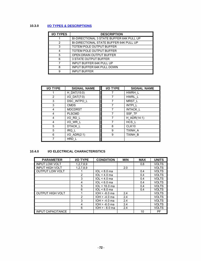
- -72
10.3.0 I/O TYPES & DESCRIPTIONS
I/O TYPES DESCRIPTION1 BI-DIRECTIONAL 3 STATE BUFFER 64K PULL UP2 BI-DIRECTIONAL STATE BUFFER 64K PULL UP3 TOTEM POLE OUTPUT BUFFER4 TOTEM POLE OUTPUT BUFFER5 OPEN DRAIN OUTPUT BUFFER6 3 STATE OUTPUT BUFFER7 INPUT BUFFER 64K PULL UP8 INPUT BUFFER 64K PULL DOWN9 INPUT BUFFER
I/O TYPE SIGNAL NAME I/O TYPE SIGNAL NAME1 H_DAT(15:0) 7 HWRH_L2 I/O_DAT(7:0) 7 HWRL_L3 DSC_INTPO_L 7 MRST_L3 CMDS 7 INTPI_L4 MDCDRST 7 INTACK_L4 PLSCMD 7 SSF_TF4 I/O_RD_L 7 H_ADR(14:1)4 I/O_WR_L 7 HCS_L5 DTACK_L 8 CLK105 IRQ_L 9 TXINH_A6 I/O_ADR(2:1) 9 TXINH_B7 HRD_L
10.4.0 I/O ELECTRICAL CHARACTERISTICS
PARAMETER I/O TYPE CONDITION MIN MAX UNITSINPUT LOW VOLT 1,2,7,8,9 0.8 VOLTSINPUT HIGH VOLT 1,2,7,8,9 2.0 VOLTSOUTPUT LOW VOLT 1 IOL < 8.0 ma 0.4 VOLTS
2 IOL < 4.0 ma 0.4 VOLTS3 IOL < 4.0 ma 0.4 VOLTS4 IOL < 6.0 ma 0.4 VOLTS5 IOL < 16.0 ma 0.4 VOLTS6 IOL < 8.0 ma 0.4 VOLTS
OUTPUT HIGH VOLT 1 IOH > -8.0 ma 2.4 VOLTS2 IOH > -4.0 ma 2.4 VOLTS3 IOH > -4.0 ma 2.4 VOLTS4 IOH > -6.0 ma 2.4 VOLTS6 IOH > - 8.0 ma 2.4 VOLTS
INPUT CAPACITANCE 10 PF
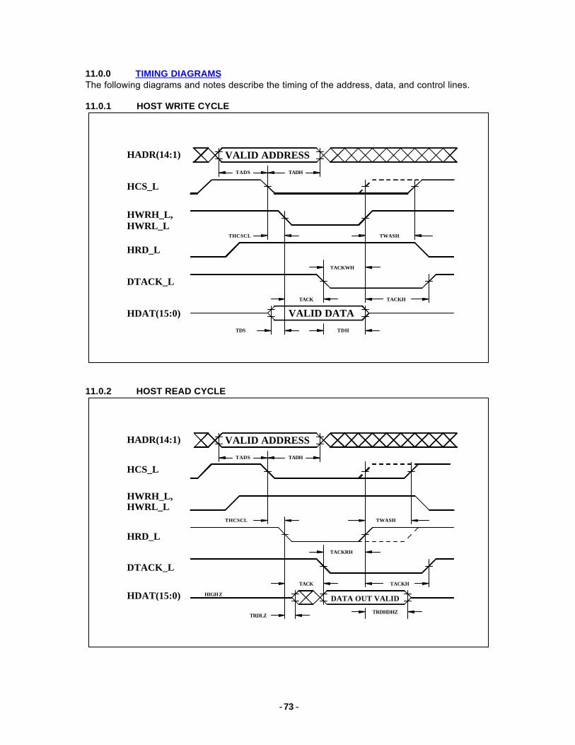
- -73
11.0.0 TIMING DIAGRAMSThe following diagrams and notes describe the timing of the address, data, and control lines.
11.0.1 HOST WRITE CYCLE
11.0.2 HOST READ CYCLE
HADR(14:1)
HCS_L
HWRH_L,HWRL_L
HRD_L
DTACK_L
HDAT(15:0)
VALID ADDRESS
VALID DATATACKH
TACKWH
THCSCL
TACK
TDHTDS
TADS TADH
TWASH
VALID ADDRESSHADR(14:1)
HCS_L
HRD_L
HWRH_L,HWRL_L
THCSCL
TACKRH
TACK TACKH
TRDHDHZTRDLZ
HIGH Z
TADHTADS
DATA OUT VALID
DTACK_L
HDAT(15:0)
TWASH
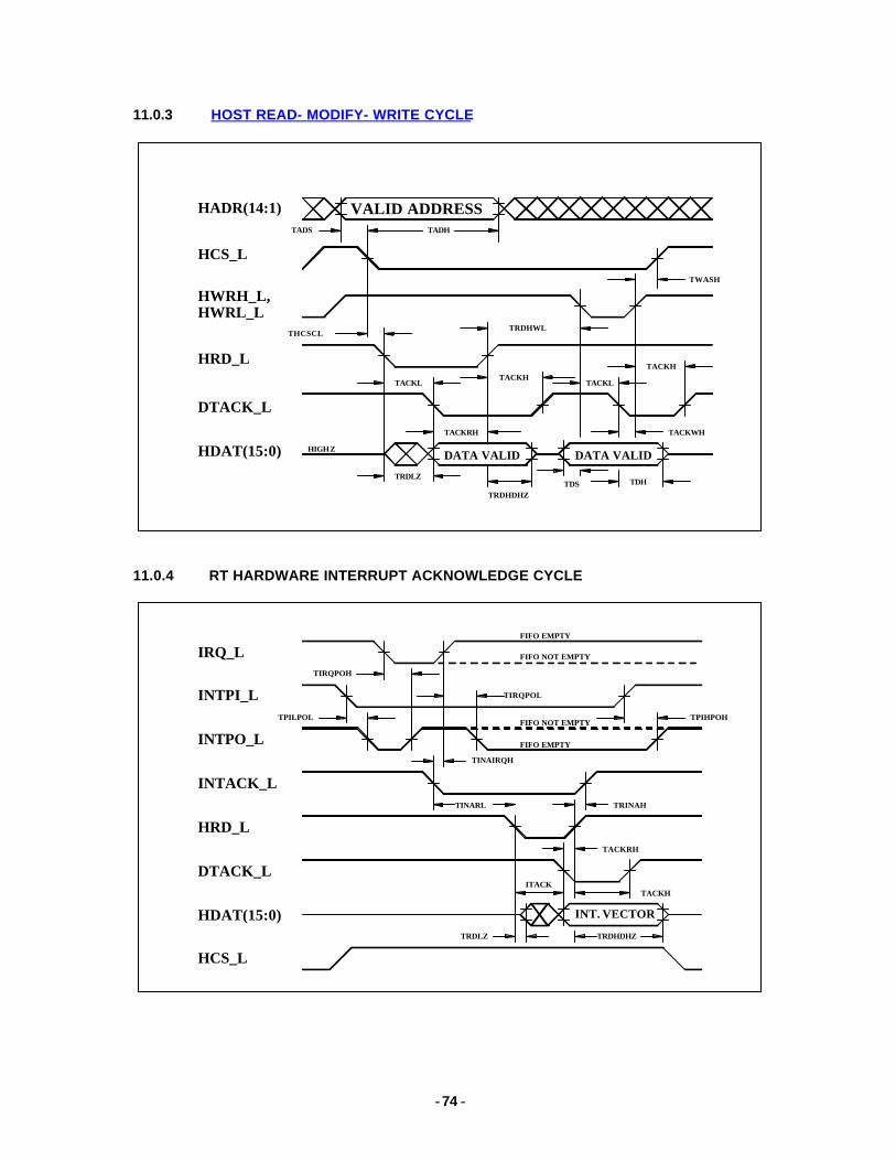
- -74
11.0.3 HOST READ- MODIFY- WRITE CYCLE
11.0.4 RT HARDWARE INTERRUPT ACKNOWLEDGE CYCLE
VALID ADDRESSHADR(14:1)
HCS_L
HRD_L
HWRH_L, HWRL_L
TACKWH
TRDLZ
HIGH Z
TADHTADS
DATA VALID
DTACK_L
HDAT(15:0) DATA VALID
TWASH
THCSCLTRDHWL
TDSTRDHDHZ
TDH
TACKRH
TACKLTACKH
TACKH
TACKL
IRQ_L
INTPI_L
INTPO_L
INTACK_L
HRD_L
DTACK_L
HDAT(15:0)
HCS_L
INT. VECTOR
FIFO NOT EMPTY
FIFO EMPTY
FIFO NOT EMPTY
TIRQPOH
TPILPOL
TINAIRQH
TPIHPOH
TRINAHTINARL
TACKRH
ITACKTACKH
TRDLZ TRDHDHZ
FIFO EMPTY
TIRQPOL
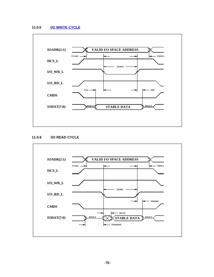
- -75
11.0.5 I/O WRITE CYCLE
11.0.6 I/O READ CYCLE
IOADR(2:1)
HCS_L
I/O_RD_L
I/O_WR_L
CMDS
IODAT(7:0)
VALID I/O SPACE ADDRESS
STABLE DATA
TVAWL
TIOWW
TWHVA
TDS TDH
HIGH ZHIGH Z
IOADR(2:1)
HCS_L
I/O_RD_L
I/O_WR_L
CMDS
IODAT(7:0)
VALID I/O SPACE ADDRESS
STABLE DATA
TVARL
TIORW
TRHVA
TRHDHZ
HIGH ZHIGH Z
TIODHZDL
TRLDS
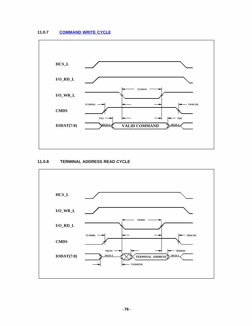
- -76
11.0.7 COMMAND WRITE CYCLE
11.0.8 TERMINAL ADDRESS READ CYCLE
HCS_L
I/O_RD_L
I/O_WR_L
CMDS
IODAT(7:0) VALID COMMAND
TCMWW
TCMHWL TWHCML
HIGH ZHIGH Z
TDS TDH
HCS_L
I/O_RD_L
I/O_WR_L
CMDS
IODAT(7:0) TERMINAL ADDRESS
TIORW
TRHCML
HIGH ZHIGH Z
TIODHZDL
TRLDS
TCMHRL
TRHDHZ
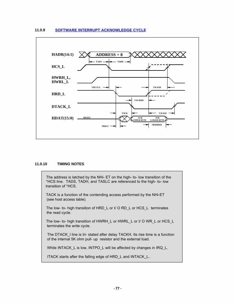
- -77
11.0.9 SOFTWARE INTERRUPT ACKNOWLEDGE CYCLE
11.0.10 TIMING NOTES
The address is latched by the NHi- ET on the high- to- low transition of the *HCS line. TADS, TADH, and TASLC are referenced to the high- to- low transition of *HCS.
TACK is a function of the contending access performed by the NHi-ET (see host access table).
The low- to- high transition of HRD_L or I/ O RD_L or HCS_L terminates the read cycle.
The low- to- high transition of HWRH_L or HWRL_L or I/ O WR_L or HCS_L terminates the write cycle.
The DTACK_l line is tri- stated after delay TACKH. Its rise time is a function of the internal 5K ohm pull- up resistor and the external load.
While INTACK_L is low, INTPO_L will be affected by changes in IRQ_L.
ITACK starts after the falling edge of HRD_L and INTACK_L..
ADDRESS = 8HADR(14:1)
HCS_L
HRD_L
HWRH_L,HWRL_L
THCSCL
TACKRH
TACK TACKH
TRDHDHZTRDLZ
HIGH Z
TADHTADS
DTACK_L
HDAT(15:0)
TWASH
AVRUPPER BYTE
IVRLOWER BYTE
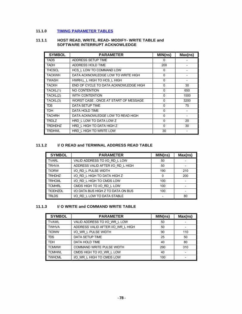
- -78
11.1.0 TIMING PARAMETER TABLES
11.1.1 HOST READ, WRITE, READ- MODIFY- WRITE TABLE and SOFTWARE INTERRUPT ACKNOWLEDGE
SYMBOL PARAMETER MIN(ns) Max(ns)TADS ADDRESS SETUP TIME 0 -TADH ADDRESS HOLD TIME 200 -THCSCL HCS_L LOW TO COMMAND LOW 0 -TACKWH DATA ACKNOWLEDGE LOW TO WRITE HIGH 0 -TWASH HWRH,L_L HIGH TO HCS_L HIGH 0 -TACKH END OF CYCLE TO DATA ACKNOWLEDGE HIGH 0 30TACKL(1) NO CONTENTION 0 650TACKL(2) WITH CONTENTION 0 1500TACKL(3) WORST CASE ; ONCE AT START OF MESSAGE 0 3200TDS DATA SETUP TIME 0 75TDH DATA HOLD TIME 0 -TACHRH DATA ACKNOWLEDGE LOW TO READ HIGH 0 -TRDLZ HRD_L LOW TO DATA LOW Z 0 20TRDHDHZ HRD_L HIGH TO DATA HIGH Z 0 30TRDHWL HRD_L HIGH TO WRITE LOW 30 -
11.1.2 I/ O READ and TERMINAL ADDRESS READ TABLE
SYMBOL PARAMETER MIN(ns) Max(ns)TVARL VALID ADDRESS TO I/O_RD_L LOW 50 -TRHVA ADDRESS VALID AFTER I/O_RD_L HIGH 50 -TIORW I/O_RD_L PULSE WIDTH 190 210TRHDHZ I/O_RD_L HIGH TO DATA HIGH Z 0 200TRHCML I/O_RD_L HIGH TO CMDS LOW 100 -TCMHRL CMDS HIGH TO I/O_RD_L LOW 100 -TIODHZDL I/O DATA BUS HIGH Z TO DATA ON BUS 100 -TRLDS I/O_RD_L LOW TO DATA STABLE - 80
11.1.3 I/ O WRITE and COMMAND WRITE TABLE
SYMBOL PARAMETER MIN(ns) Max(ns)TVAWL VALID ADDRESS TO I/O_WR_L LOW 50 -TWHVA ADDRESS VALID AFTER I/O_WR_L HIGH 50 -TIOWW I/O_WR_L PULSE WIDTH 90 110TDS DATA SETUP TIME 25 50TDH DATA HOLD TIME 40 80TCMWW COMMAND WRITE PULSE WIDTH 290 310TCMHWL CMDS HIGH TO I/O_WR_L LOW 40 -TWHCML I/O_WR_L HIGH TO CMDS LOW 100 -
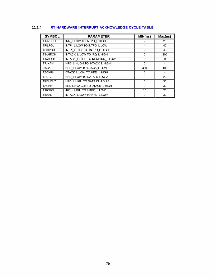
- -79
11.1.4 RT HARDWARE INTERRUPT ACKNOWLEDGE CYCLE TABLE
SYMBOL PARAMETER MIN(ns) Max(ns)TIRQPOH IRQ_L LOW TO INTPO_L HIGH - 20TPILPOL INTPI_L LOW TO INTPO_L LOW - 40TPIHPOH INTPI_L HIGH TO INTPO_L HIGH - 40TINAIRQH INTACK_L LOW TO IRQ_L HIGH 0 200TINAIRQL INTACK_L HIGH TO NEXT IRQ_L LOW 0 200TRINAH HRD_L HUGH TO INTACK_L HIGH 0 -ITACK HRD_L LOW TO DTACK_L LOW 300 400TACKRH DTACK_L LOW TO HRD_L HIGH 0 -TRDLZ HRD_L LOW TO DATA IN LOW Z 0 20TRDHDHZ HRD_L HIGH TO DATA IN HIGH Z 0 30TACKH END OF CYCLE TO DTACK_L HIGH 0 30TIRQPOL IRQ_L HIGH TO INTPO_L LOW 10 20TINARL INTACK_L LOW TO HRD_L LOW 0 30
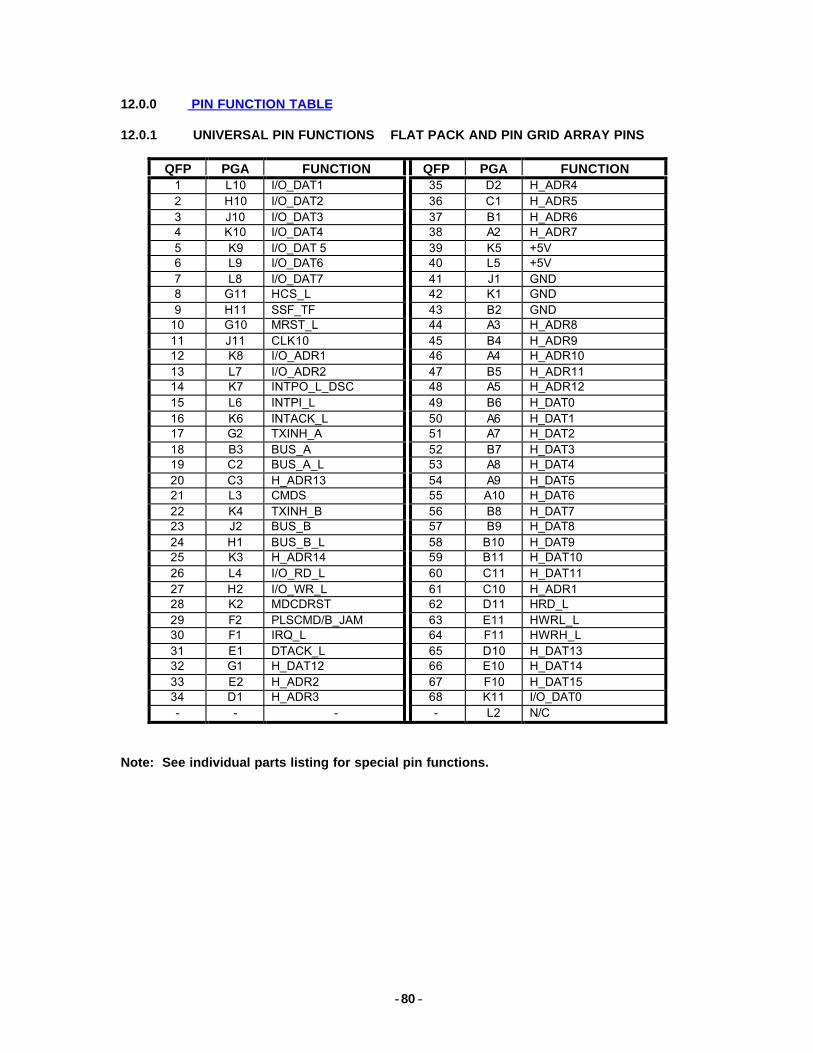
- -80
12.0.0 PIN FUNCTION TABLE
12.0.1 UNIVERSAL PIN FUNCTIONS FLAT PACK AND PIN GRID ARRAY PINS
QFP PGA FUNCTION QFP PGA FUNCTION1 L10 I/O_DAT1 35 D2 H_ADR42 H10 I/O_DAT2 36 C1 H_ADR53 J10 I/O_DAT3 37 B1 H_ADR64 K10 I/O_DAT4 38 A2 H_ADR75 K9 I/O_DAT 5 39 K5 +5V6 L9 I/O_DAT6 40 L5 +5V7 L8 I/O_DAT7 41 J1 GND8 G11 HCS_L 42 K1 GND9 H11 SSF_TF 43 B2 GND
10 G10 MRST_L 44 A3 H_ADR811 J11 CLK10 45 B4 H_ADR912 K8 I/O_ADR1 46 A4 H_ADR1013 L7 I/O_ADR2 47 B5 H_ADR1114 K7 INTPO_L_DSC 48 A5 H_ADR1215 L6 INTPI_L 49 B6 H_DAT016 K6 INTACK_L 50 A6 H_DAT117 G2 TXINH_A 51 A7 H_DAT218 B3 BUS_A 52 B7 H_DAT319 C2 BUS_A_L 53 A8 H_DAT420 C3 H_ADR13 54 A9 H_DAT521 L3 CMDS 55 A10 H_DAT622 K4 TXINH_B 56 B8 H_DAT723 J2 BUS_B 57 B9 H_DAT824 H1 BUS_B_L 58 B10 H_DAT925 K3 H_ADR14 59 B11 H_DAT1026 L4 I/O_RD_L 60 C11 H_DAT1127 H2 I/O_WR_L 61 C10 H_ADR128 K2 MDCDRST 62 D11 HRD_L29 F2 PLSCMD/B_JAM 63 E11 HWRL_L30 F1 IRQ_L 64 F11 HWRH_L31 E1 DTACK_L 65 D10 H_DAT1332 G1 H_DAT12 66 E10 H_DAT1433 E2 H_ADR2 67 F10 H_DAT1534 D1 H_ADR3 68 K11 I/O_DAT0- - - - L2 N/C
Note: See individual parts listing for special pin functions.
- -81
12.1.0 GENERIC PACKAGE OUTLINE DRAWINGS
12.1.1 QUAD FLAT PACK UNFORMED LEAD
12.1.2 QUAD FLAT PACK GULL WING LEADS
68 PLCS.
9
681
61
CH
10 26.018 ±.002
USA 27
NHI-15XXXXXGW
57363
NATIONAL HYBRID
NHi
60 44
43
0.085 REF
1.270 MIN
.050TYP
.800 ±.010
1.360 ±.015
0.010 ±.005
0.045 ±.015
1.100 ±.010
NATIONAL HYBRID
NHI-15XXXXXFP
57363
USA
CH
HiN
.018 ±.00268 PLCS.
61
9
168
27
43
10 26
4460
.400MIN. .010 ±.002
.155 MAX.
.065 ±.010
SEATING ANDBASE PLANE
.800 ±.010
.050TYP
1.100 ±.010
- -82
12.1.3 PIN GRID ARRAY
USA
57363
NHI-15XXXXX
NATIONAL HYBRID
CH
NHi
SEATING PLANE
SEATING PLANE
1.030 ±.010
1.080 ±.010
1.100 ±.010
.065 DIA. .018 ±.002
.220 MIN.
.150 MAX.
1.000 ±.010.050TYP
.100TYP
TYP TYP
- -83
12.1.4 MICRO QUAD FLAT PACK UNFORMED LEADS
12.1.5 MICRO QUAD FLAT PACK GULL WING LEADS
68 PLCS.
9
681
61
CH
10 26.018 ±.002
USA 27
NHI-15YYYYYGW
57363
NATIONAL HYBRID
NHi
60 44
43
0.085 REF
1.120 MIN
.050TYP
.800 ±.010
0.950 ±.010
0.010 ±.005
1.210 ±.015
0.045 ±.015
NATIONAL HYBRID
NHI-15YYYYYFP
57363
USA
CH
HiN
.018 ±.002
0.950 ±.010
68 PLCS.
61
9
168
27
43
10 26
4460
.400MIN.
.155 MAX.
.065 ±.010
SEATING ANDBASE PLANE
.050TYP
.800 ±.010
.010 ±.002
- -84
13.0.0 MATING TRANSFORMER REFERENCEAll the NHi-ET requires a coupling transformer with a turns ratio of 1: 2.5 for Direct Coupling, anda turns ratio of 1: 1.79 for Transformer Coupling to the Mil- Std Data Bus. Please contact BetaTransformer ( www.bttc-beta.com ) for a recommended transformer.
The center tap on the NHi-ET side of the coupling transformer must be grounded. The center tapon the bus side of the coupling transformer should be left floating.
The figure shows a typical transformer connection.
NHI-1582ET
BUS
BUS_L
NHI-1582ET
BUS
BUS_L
TRANSFORMER COUPLED
DIRECT COUPLED
1 : 1.79 1 : 1.4
1 : 2.5 .75Zo
.75Zo
.75Zo
.75Zo
Zo
Zo
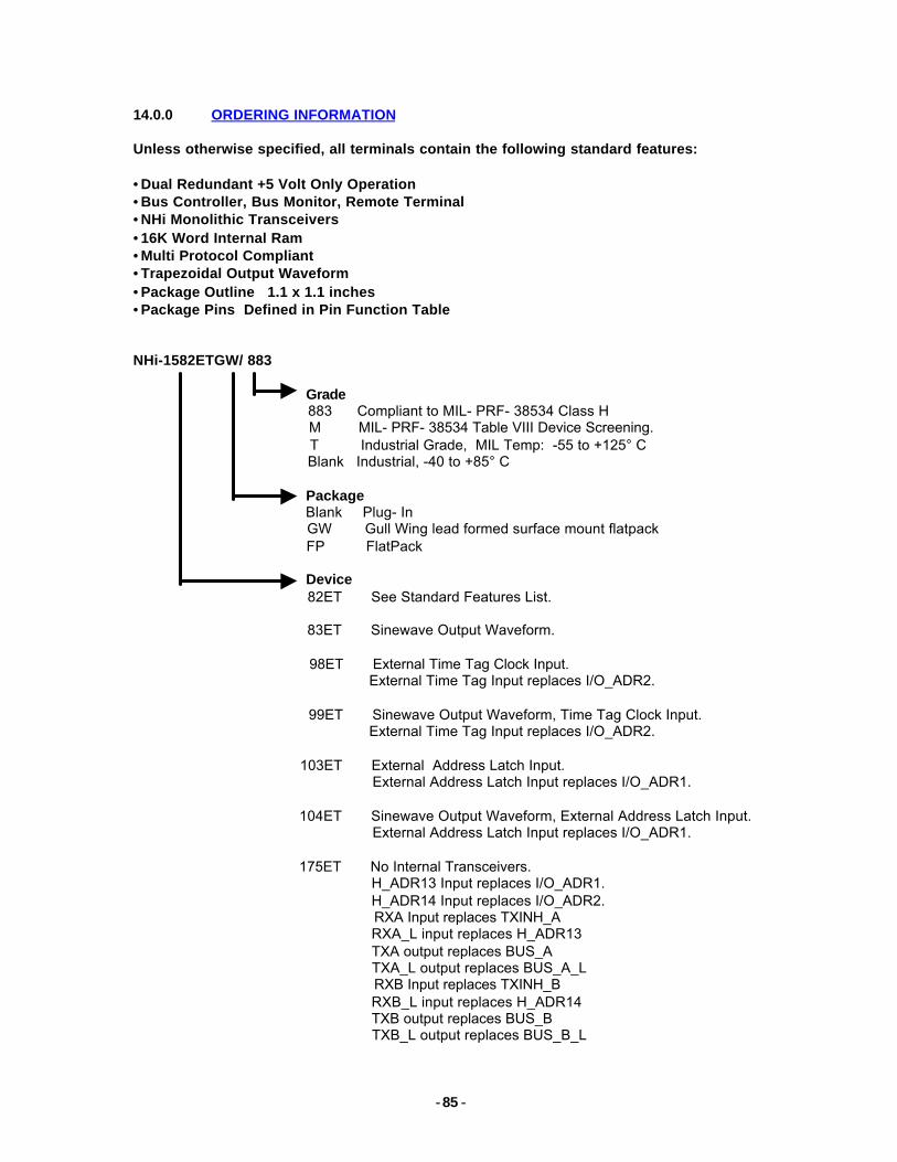
- -85
14.0.0 ORDERING INFORMATION
Unless otherwise specified, all terminals contain the following standard features:
•Dual Redundant +5 Volt Only Operation•Bus Controller, Bus Monitor, Remote Terminal•NHi Monolithic Transceivers•16K Word Internal Ram•Multi Protocol Compliant•Trapezoidal Output Waveform•Package Outline 1.1 x 1.1 inches•Package Pins Defined in Pin Function Table
NHi-1582ETGW/ 883
Grade 883 Compliant to MIL- PRF- 38534 Class H M MIL- PRF- 38534 Table VIII Device Screening. T Industrial Grade, MIL Temp: -55 to +125° C Blank Industrial, -40 to +85° C
Package Blank Plug- In GW Gull Wing lead formed surface mount flatpack FP FlatPack
Device 82ET See Standard Features List.
83ET Sinewave Output Waveform.
98ET External Time Tag Clock Input. External Time Tag Input replaces I/O_ADR2.
99ET Sinewave Output Waveform, Time Tag Clock Input. External Time Tag Input replaces I/O_ADR2.
103ET External Address Latch Input. External Address Latch Input replaces I/O_ADR1.
104ET Sinewave Output Waveform, External Address Latch Input. External Address Latch Input replaces I/O_ADR1.
175ET No Internal Transceivers. H_ADR13 Input replaces I/O_ADR1. H_ADR14 Input replaces I/O_ADR2. RXA Input replaces TXINH_A RXA_L input replaces H_ADR13 TXA output replaces BUS_A TXA_L output replaces BUS_A_L RXB Input replaces TXINH_B RXB_L input replaces H_ADR14 TXB output replaces BUS_B TXB_L output replaces BUS_B_L
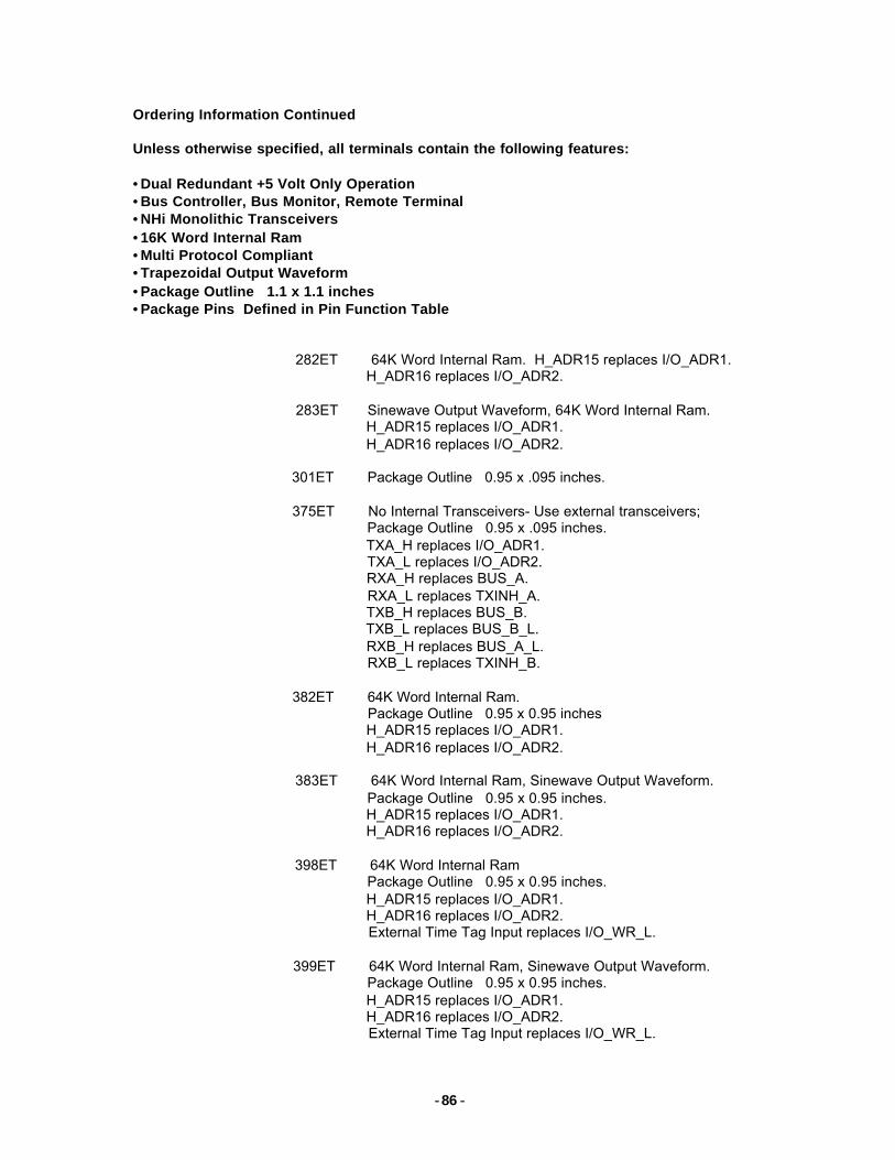
- -86
Ordering Information Continued
Unless otherwise specified, all terminals contain the following features:
•Dual Redundant +5 Volt Only Operation•Bus Controller, Bus Monitor, Remote Terminal•NHi Monolithic Transceivers•16K Word Internal Ram•Multi Protocol Compliant•Trapezoidal Output Waveform•Package Outline 1.1 x 1.1 inches•Package Pins Defined in Pin Function Table
282ET 64K Word Internal Ram. H_ADR15 replaces I/O_ADR1. H_ADR16 replaces I/O_ADR2.
283ET Sinewave Output Waveform, 64K Word Internal Ram. H_ADR15 replaces I/O_ADR1. H_ADR16 replaces I/O_ADR2.
301ET Package Outline 0.95 x .095 inches.
375ET No Internal Transceivers- Use external transceivers; Package Outline 0.95 x .095 inches. TXA_H replaces I/O_ADR1. TXA_L replaces I/O_ADR2. RXA_H replaces BUS_A. RXA_L replaces TXINH_A. TXB_H replaces BUS_B. TXB_L replaces BUS_B_L. RXB_H replaces BUS_A_L. RXB_L replaces TXINH_B.
382ET 64K Word Internal Ram. Package Outline 0.95 x 0.95 inches H_ADR15 replaces I/O_ADR1. H_ADR16 replaces I/O_ADR2.
383ET 64K Word Internal Ram, Sinewave Output Waveform. Package Outline 0.95 x 0.95 inches. H_ADR15 replaces I/O_ADR1. H_ADR16 replaces I/O_ADR2.
398ET 64K Word Internal Ram Package Outline 0.95 x 0.95 inches. H_ADR15 replaces I/O_ADR1. H_ADR16 replaces I/O_ADR2. External Time Tag Input replaces I/O_WR_L.
399ET 64K Word Internal Ram, Sinewave Output Waveform. Package Outline 0.95 x 0.95 inches. H_ADR15 replaces I/O_ADR1. H_ADR16 replaces I/O_ADR2. External Time Tag Input replaces I/O_WR_L.
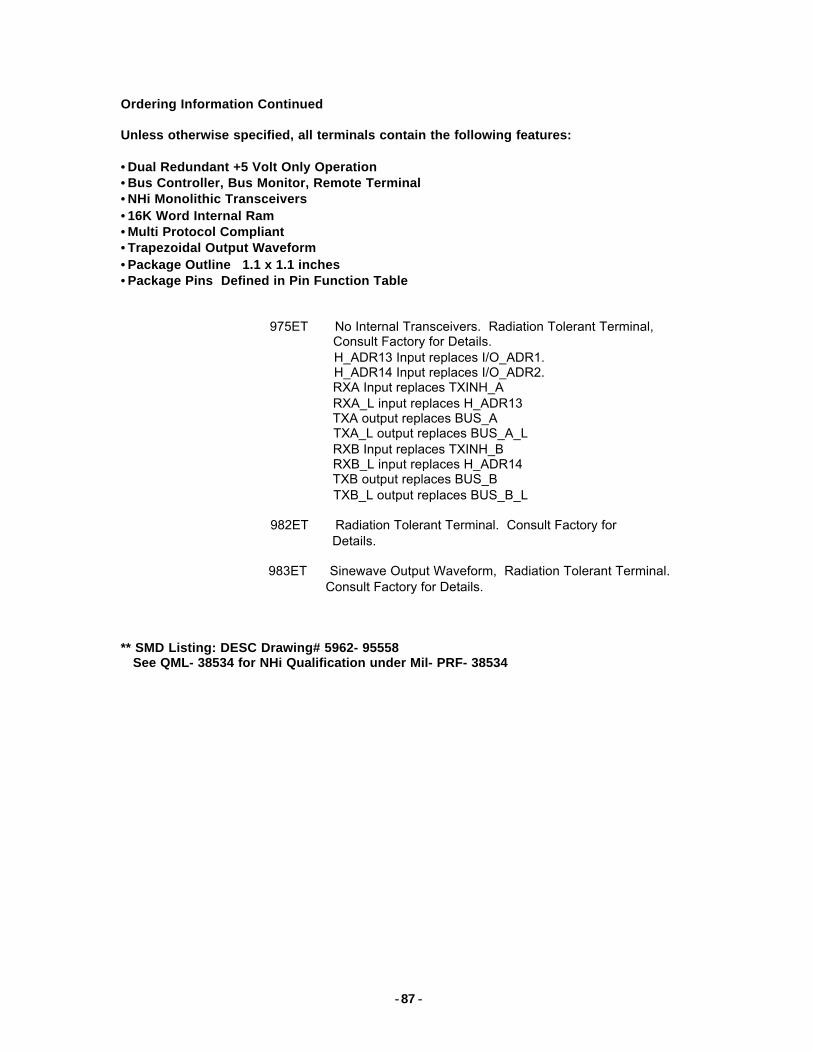
- -87
Ordering Information Continued
Unless otherwise specified, all terminals contain the following features:
•Dual Redundant +5 Volt Only Operation•Bus Controller, Bus Monitor, Remote Terminal•NHi Monolithic Transceivers•16K Word Internal Ram•Multi Protocol Compliant•Trapezoidal Output Waveform•Package Outline 1.1 x 1.1 inches•Package Pins Defined in Pin Function Table
975ET No Internal Transceivers. Radiation Tolerant Terminal, Consult Factory for Details. H_ADR13 Input replaces I/O_ADR1. H_ADR14 Input replaces I/O_ADR2. RXA Input replaces TXINH_A RXA_L input replaces H_ADR13 TXA output replaces BUS_A TXA_L output replaces BUS_A_L RXB Input replaces TXINH_B RXB_L input replaces H_ADR14 TXB output replaces BUS_B TXB_L output replaces BUS_B_L
982ET Radiation Tolerant Terminal. Consult Factory for Details.
983ET Sinewave Output Waveform, Radiation Tolerant Terminal. Consult Factory for Details.
** SMD Listing: DESC Drawing# 5962- 95558 See QML- 38534 for NHi Qualification under Mil- PRF- 38534

The information in this Manual is believed to be accurate; however, no responsibility is assumed by Data Device Corporation for its use, and no license or rights are granted by implication or otherwise in connection therewith. Specifications are subject to change without notice.
Outside the U.S. - Call 1-631-567-5600
United Kingdom: DDC U.K., LTD Mill Reef House, 9-14 Cheap Street, Newbury, Berkshire RG14 5DD, England Tel: +44 1635 811140 Fax: +44 1635 32264
France: DDC Electronique 10 Rue Carle-Hebert 92400 Courbevoie France Tel: +33-1-41-16-3424 Fax: +33-1-41-16-3425
Germany: DDC Elektronik GmbH Triebstrasse 3, D-80993 München, Germany Tel: +49 (0) 89-15 00 12-11 Fax: +49 (0) 89-15 00 12-22
Japan: DDC Electronics K.K. Dai-ichi Magami Bldg, 8F, 1-5, Koraku 1-chome, Bunkyo-ku, Tokyo 112-0004, Japan Tel: 81-3-3814-7688 Fax: 81-3-3814-7689 Web site: www.ddcjapan.co.jp
Asia: Data Device Corporation - RO Registered in Singapore Blk-327 Hougang Ave 5 #05-164 Singapore 530327 Tel: +65 6489 4801
Inside the U.S. - Call Toll-Free 1-800-DDC-5757
Headquarters and Main Plant 105 Wilbur Place, Bohemia, NY 11716-2426 Tel: (631) 567-5600 Fax: (631) 567-7358 Toll-Free, Customer Service: 1-800-DDC-5757
Web site: www.ddc-web.com
DATA DEVICE CORPORATIONREGISTERED TO:
ISO 9001:2008, AS9100C:2009-01EN9100:2009, JIS Q9100:2009
FILE NO. 10001296 ASH09
RE
GIS T E R E D F
IRM
®U
The first choice for more than 45 years—DDC DDC is the world leader in the design and manufacture of high reliability data interface products, motion control, and solid-state power controllers for aerospace, defense, and industrial automation.