Embed Size (px)
Citation preview
Nano Packaging Technology for Interconnect and Heat Dissipation
NANOPACK
Large-Scale Integrating Project Start Date : 01/11/07 Project n° 216176 Duration : 36 months THEME 3 : Information and Communication Technologies
WORK PACKAGE 1 : Systems and applications specifica tions
DELIVERABLE D1.2 Decision on material pairings and geometrical
set-up for test-specimens and test systems
Due date : T0+6 Submission date : T0+6
Lead contractor for this deliverable : BME
Dissemination level : PU – Public

D1.2 version 00
2/30
WORK PACKAGE 1 : Systems and applications specifications
TASK 1.2 Decision on material pairings and geometrical set-u p for
test-specimens and test systems
PARTNERS ORGANISATION APPROVAL
Name Function Date Signature
Prepared by: M.Rencz WP4 leader
Approved by:
WP MANAGEMENT TEAM APPROVAL
Entity Name Date Signature
Approved by: TRT Afshin Ziaei
Approved by: BME Marta Rencz
Approved by: Bosch Klaus-Volker Schuett
Approved by: IEMN B. Djafari-Rouhani
Approved by: Chalmers Johan Liu
Approved by: EVAC Xinhe Tang
Approved by: FOAB Bjorn Carlberg
Approved by: F-IZM Bernhard Wunderle
Approved by: IBM Bruno Michel
Approved by: ICN Clivia Sotomayor
Approved by: MicReD Andras Poppe
Approved by: Nanotest Thomas Winkler
Approved by: THAV Claude Sarno
Approved by: VTT Mika Prunnila
D1.2 version 00
3/30
DISTRIBUTION LIST
WORK PACKAGE 1 : SYSTEMS AND APPLICATIONS SPECIFICATIONS
TASK 1.2
Decision on material pairings and geometrical set-up for test-specimens and test systems
QUANTITY
ORGANIZATION NAMES
1 ex
1 ex
1 ex
1 ex
1 ex
1 ex
1 ex
1 ex
1 ex
1 ex
1 ex
1 ex
1 ex
1 ex
1 ex
CEC
Thales Research and Technology
Budapest University of Technology & Economics
Robert Bosch GmbH
CNRS (Institut d’Electronique de Microtechnologie et de Nanotechnologie
Chalmers Tekniska Högskola AB
Electrovac AG
FOAB Elektronik AB
Fraunhofer Gesellschaft zur Förderung der Angewandten Forschung eV
IBM Research GmbH
Fundacio Privada Institut Catala de Nanotecnologia
Microelectronics Research and Development GmbH
Berliner Nanotest und Design GmbH
Thales Avionics SA
Valtion Teknillinen Tutkimuskeskus
TRT
BME
Bosch
IEMN
Chalmers
EVAC
FOAB
F-IZM
IBM
ICN
MivReD
Nanotest
THAV
VTT
Isabel Vergara Ogando
Afshin Ziaei
Marta Rencz
Klaus-Volker Schuett
Bahram Djafari-Rouhani
Johan Liu
Xinhe Tang
Björn Carlberg
Bernhard Wunderle
Bruno Michel
Clivia Sotomayor
Andras Poppe
Thomas Winkler
Claude Sarno
Mika Prunnila
D1.2 version 00
4/30
CHANGE RECORD SHEET
REVISION LETTER DATE PAGE NUMBER DESCRIPTION
Draft 20/01/2008 Draft version
00 17/04/08 30 Initial version
D1.2 version 00
5/30
CONTENTS 1 ABBREVIATION / DEFINITION.......................... .......................................................................... 7
2 INTRODUCTION........................................................................................................................... 8
3 DECISION OF MATERIAL PAIRINGS ...................... ................................................................... 9
4 GEOMETRICAL SET-UPS FOR TEST SPECIMEN USED IN THE DIFFERENT TESTING METHODS ......................................................................................................................................... 11
4.1 GEOMETRICAL SET-UPS FOR 3-OMEGA AND STEADY STATE TECHNIQUES (BME, F-IZM, IBM, MICRED, VTT, ICN) ........................................................................................................................ 11
4.1.1 Geometrical set-up for the 3-omega technique .............................................................. 11 4.1.2 Geometrical set-ups for the steady state techniques ..................................................... 12
4.2 TEST STRUCTURE TO INVESTIGATE PACKED PARTICLE ELECTRICAL AND THERMAL INTERCONNECTS (IBM, F-IZM, NANOTEST) ................................................................................................................. 14 4.3 THIN FILM MICRO-SCALE HEATER/SENSOR DEVICES (TRT, IEMN, CHALMERS, F-IZM) .............. 14 4.4 DEVELOPMENT OF THIN GAP SQUEEZE ASSEMBLY STANDS (CHALMERS, FOAB, EVAC, NANOTEST, TRT) 20 4.5 DEVELOPMENT OF A SAMPLE HOLDER DESIGN ESPECIALLY FOR IN SITU THERMAL TRANSIENT MEASUREMENT OF THIN MATERIALS (BME, MICRED, EVAC)............................................................. 21
5 TEST VEHICLES USED AS FINAL DEMONSTRATORS IN WP7 ... ......................................... 22
5.1 THAV TEST VEHICLES THAT WILL BE USED FOR THE FINAL EVALUATION IN WP7 ........................ 22 5.2 IBM MICROPROCESSOR TEST VEHICLES ................................................................................. 26 5.3 BOSCH TEST VEHICLES THAT WILL BE USED FOR THE FINAL EVALUATION IN WP7....................... 27 5.4 TRT TEST VEHICLE................................................................................................................. 27
6 CONCLUSION ............................................................................................................................ 29
REFERENCES .................................................................................................................................. 30
D1.2 version 00
6/30
FIGURES
Figure 1: Schematic of possible designs for heater/thermometer (red) and contact pads (blue) 11 Figure 2: The planned steady-state assembly of BME and MicReD 13 Figure 3 : Flip chip microprocessor TIM1 test vehicle. 13 Figure 4: Research test stand for investigation of interface material thermal and electrical properties.
14 Figure 5 : Technological possibilities for T-sensors, flow-sensors and heaters 15 Figure 6 : Improved set-up with best temperature resolution 16 Figure 7 : Improved set-up with best reproducibility and possibilities for surface enhancement 16 Figure 8 : Possible structure for heater (2-point) and temperature sensors (4-point) 17 Figure 9 : Specific electrical resistivity ρ and temperature coefficient TCR for several metals 17 Figure 10: Temperature dependence of electrical resistivity for chromium, tungsten and molybdenum.
18 Figure 11 : Preliminary selected materials for heater and temperature sensors, considered design rule
and electrical properties 18 Figure 12: Design schematic 19 Figure 13: Preliminary sketch of potential test setup 19 Figure 14 : Schematic of heater and temperature sensor structures. 19 Figure 15 : Potential interconnection schemes 20 Figure 16 : Schematic of measurement setup: Thermal flow density and expected temperature drop20 Figure 17: The proposed fixture for real time applications 21 Figure 18 The final demonstrator used by Thales 22 Figure 19 : Electrical scheme for chip management 24 Figure 20: Thermally enhanced PQFP with embedded heat spreader 24 Figure 21: The RT020 resistor 25 Figure 22: SEB cooling with Heat Pipes and Loop Heat Pipes 25 Figure 23: Mounting on the heat pipes 26 Figure 24 : Microprocessor Test Vehicle used to estimate TIM performance in application
environment. 26 Figure 25 : Electrical control unit with logic circuit (centre) and three surrounding power circuits 27 Figure 26: Non packaged RF-MEMS capacitive shunt switch 27 Figure 27: Topology and materials used for RF-MEMS capacitive shunt switch 28 Figure 28: Figure: Images of packaged RF-MEMS switches, before and after die separation 29
TABLES
Table 1 : Schematic of possible material pairings 10 Table 2: Encapsulated dies specifications 23
D1.2 version 00
7/30
1 ABBREVIATION / DEFINITION
TIM Thermal Interface Material SOI Silicon On Insulator CNT Carbon Nano Tube BLT Bond Line Thickness MCM Multi-Chip Module LCC Life Cycle Cost SCM Single-Chip Module Rth Thermal Resistance HP Heat Pipe BN Boron Nitride PAO Poly Alpha Olefins PDMS Poly Dimethyl Siloxans RTD Resistive Thermal Device NP Nano Particles SEB Seat Electronic Box

D1.2 version 00
8/30
2 INTRODUCTION This deliverable defines the final decision of the consortium members about the material parings used in TIM materials, and about the test specimen and test systems used in the final evaluation of the TIM materials that will have been developed in the NANOPACK project. TIM material testing has three significantly different applications. On one hand TIM quality has to be checked during the material development phase. For this purpose experimental methods are needed, that can be lengthy and complicated, but need to be very accurate. On the other hand standardized industrial methods are needed to compare the quality of the TIM material of different TIM vendors to qualify them for certain applications. The standardized methods have to be able to qualify on one hand again the TIM material in itself, on the other hand methods are needed to verify and compare the quality of the TIM in real life applications [1]. These are called in our document the “in situ” measurements. In the NANOPACK project we will develop methodologies and test structures both for the experimental and the industrial methods, this explains the diversity of the test structures that are aimed to be developed in WP4 of the NANOPACK project. The statements of this deliverable are the result of the first 3 months research of the individual consortium partners, discussed in details at the first WP4 meeting at 21/01/2008 Budapest. The decision about material pairings for particle filled materials is presented in Chapter 3. Chapter 4 defines the final decision of the partners about the various geometrical set-ups for test specimen used in the different testing methods. The final demonstrators are presented in Chapter 5.

D1.2 version 00
9/30
3 DECISION OF MATERIAL PAIRINGS In the framework of the NANOPACK research the following material pairings will be used for particle filled materials: Matrix material viscosity at 40C: >20 cSt Common thermal grease oils: Hydrocarbon based: PAO (poly alpha olefins), Silicone based: PDMS (poly dimethyl siloxane) Thermal pad Phase change materials Thermal and electrical adhesive: Matrix: silicone elastomers (more flexible for improved cycling) and epoxies (stronger adhesion with poor cycling) Particle systems: Size range: <20um Bi or Tri-modal systems preferred Electrical materials: Graphite, Silver, CNT, SiC, BN, Thermal materials: Aluminum, Aluminum oxide, Graphite, Dispersants and surfactants: Steric acid,
COMMENTS: If too many different materials are used there will be high Kapitza resistances between the many material mismatches in the thermal path. Need more information on alternative materials: CNT based systems, Gold nanograss (fill factors, height, adhesion/seed layers…)
Bosch will use commercially available TIM2 materials (to be selected after finishing T2.1) as well as materials developed by project partners in WP2. Mating surfaces have been selected from current Bosch products:
• Heat sink materials: Copper (milled), Aluminum alloy (die casted, e.g. AlSi8Cu3SF, AlMgSi1, AlSi12(Fe))
• Circuit materials: Copper (etched), Alumina These surfaces exhibit certain roughness as well as different oxides that will create a certain thermal contact resistance. Our aim is to quantify the contact resistance in dependence of process steps prior to heat sink attachment (e.g. die casting, shot blasting, milling, etc.).
D1.2 version 00
10/30
Schematic of possible material pairings for 3ω method and micro Raman scattering (silicon – orange, oxide – green)
Structures Impact
Reference systems, through-plane phonon transmission
Impact of roughness on thermal characteristics before deposition of nano-particles (NPs)
Evaluation of pastes with NPs as thermal interfaces.
Heat dissipation in presence of hot spots.
Table 1 : Schematic of possible material pairings
D1.2 version 00
11/30
4 GEOMETRICAL SET-UPS FOR TEST SPECIMEN USED IN THE DIFFERENT TESTING METHODS
4.1 GEOMETRICAL SET-UPS FOR 3-OMEGA AND STEADY STATE TECHNIQUES (BME, F-IZM, IBM, MICRED, VTT, ICN)
4.1.1 Geometrical set-up for the 3-omega technique 3ω-method
Physical dimensions: Sample width: 5 mm to 20mm Sample length: 5 mm to 20mm Sample height: up to 2 mm Sample thickness: 5 times the thermal penetration depth
Heater/thermometer needs: For sample thickness greater than 1µm (2D heat wave model):
Line width: 5 times smaller than film/sample thickness, Line length: 20 times longer than film/sample thickness, For sample thickness less than 1µm (1D heat wave model): Line width: 5 times greater than film/sample thickness, Line length: 20 times longer than film/sample thickness, Material for heater/thermometer: Platinum, Nickel, Gold, Molybdenum, Aluminium 4 contact pads bigger than 100µm x 100µm or alternative 2 rectangular contact pads bigger than 300µm x 100µm needed for 4-probe measurement set-up
Figure 1: Schematic of possible designs for heater/thermometer (re d) and contact pads (blue)
V+
I-
I+
V-
V+
I-
I+
V-
V+
I-
I+
V-
D1.2 version 00
12/30
Micro Raman scattering
Physical dimensions: Sample width: 1 mm to 15 mm Sample length: 1 mm to 15 mm Sample height: less than 2 mm
4.1.2 Geometrical set-ups for the steady state tech niques Steady state TIM testing methods may be useful both as experimental methods during material development and methods that may be used for the comparison of TIM material from different producers in a standardized environment. The versatility of the method explains that steady state methods will be pursued by different partners. The test set-ups of the different partners are presented below. BME, Micred: Steady-state TIM tester ( Figure 2 ) Expected specification Active area: 12.5×12.5 mm2 (or 10×10 mm2)
Heat flux & temperature measurement using the same monolithic dice
Heat flux: max. 20 W (40 W ?) conveyed by Peltier cells
Heat flux accuracy: ± 0.1 W
Resolution of temperature difference measurement
0.006 K
Resolution of TIM Rth measurement 0.03 ÷ 0.04 Kmm2/W
TIM Rth measurement 2 ÷ 5 Kmm2/W ± 5 ÷ 10 %
Mechanical pressure max. 2⋅105 N/m2
TIM thickness measurement optic (?)
Special feature: symmetric arrangement, reversible heat-flow direction

D1.2 version 00
13/30
Figure 2: The planned steady-state assembly of BME and MicReD
Testing Methods for IBM microprocessor TIM1 and TIM 2 applications IBM Zurich Research Laboratory will utilize several different test methods to evaluate interface material properties and application performance. Product like test vehicles will be used for demonstrator type performance measurements and research test devices will be used to explore bulk material and particle stack properties. The application test vehicle resembles a typical flip chip packaged Silicon die with heater and sensor array on the opposite side as the TIM and lid/cooler surface as shown in Figure 3.
T1
TIM BONDLINETHICKNESSSENSORS
LIQUIDCOOLER
COOLERHOLDER
HEATER & SENSORLITHOGRAPHY
Silicon
PCB or CHIP CARRIER
T2
Figure 3 : Flip chip microprocessor TIM1 test vehicle. Due to the thick silicon chip and variability in cooler performance, this test vehicle is only capable of providing average bondline performance data without localized information on non-uniformities in the bondline due to voids or particle stacking. Heating at the lower surface of the silicon is accomplished using a meandering thin film heater (~30nm gold) with interspersed resistive thermal devices (RTD) also based on meandering serpentine structures with 4-point connections (~30nm thick, 10um wide metal line). This allows a single metallization step to define heater and sensor devices. The typical resistance of a thin film RTD sensor is approximately 150 Ohm with a sensitivity of 0.5ºC/Ohm . Total thermal resistance or junction-to-air resistance is determined based on the temperature difference between the chip sensors and a set cooler temperature divided by the total power dissipated. In order to estimate the interface resistance, the thermal resistance of the silicon and water cooler must be known or determined from additional calibration experiments and subtracted from the total resistance (often inducing the largest uncertainty). Inductive based displacement sensors, calibrated to zero before the interface material is applied, track the thickness of the interface as estimated from 4 points along the periphery of the system. Overall accuracy of interface resistance estimation is typically on the order of +-1Cmm 2/W. This test stand can also be used as an application demonstrator when a chip lid is inserted between the chip and cooler surface. With the lid inserted, the effect of a larger TIM2 area can also be investigated.
D1.2 version 00
14/30
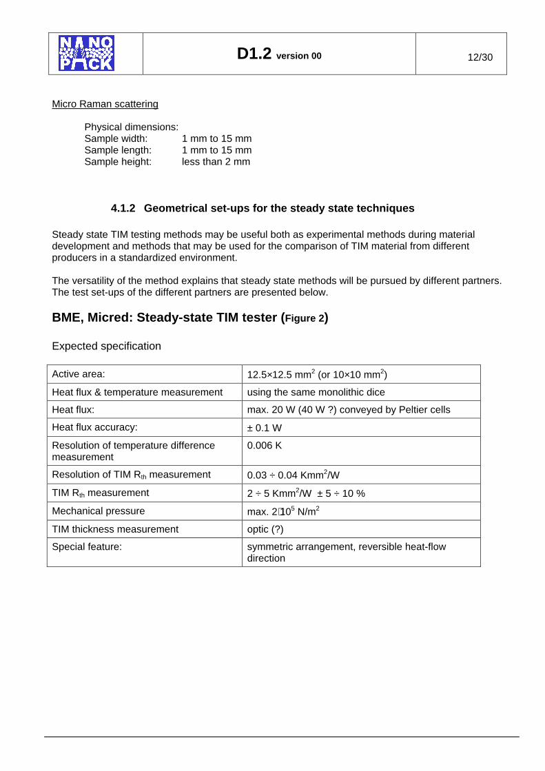
4.2 TEST STRUCTURE TO INVESTIGATE PACKED PARTICLE
ELECTRICAL AND THERMAL INTERCONNECTS (IBM, F-IZM, NANOTEST)
In order to increase the accuracy and area resolution of a thermal test an alternative test system will be developed with the capability to measure both thermal and electrical properties directly at both sides of the interface. This system uses two rectangular sensor chips with RTD sensors directly on both sides of the interface as shown in Figure 4. Heat is introduced below the chip stack by a thin film heater and a cooler is applied to the top of the chip stack. The temperature drop across the interface at specific locations is then measured by the RTD sensors, which have a similar design and performance as the test vehicle shown in Figure 3. In order to measure electrical resistance across the interface, the RTD is replace by a simple electrode with two contacts and a small current is applied between the upper and lower electrode allowing a 4-point measurement of voltage and current drop across the thin gap. An array of numerous sensors across the interface allows for investigation at locations that are known to have particle stacking non-uniformities such as the center point and along the lines between opposite corners of the square interface area.
LIQUIDCOOLER
V ,2 T2
V ,T1 1
HEATER
Figure 4: Research test stand for investigation of interface mat erial thermal and electrical properties.
IBM will use the test device shown in Figure 4 with a test chip combination that allows comparison between the region of particle stacking (“x” between chip corners) and the non-stacking or bulk regions. Preliminary results have already shown the test stand is capable of resolving small differences in temperature and electrical gradient between the two regions.
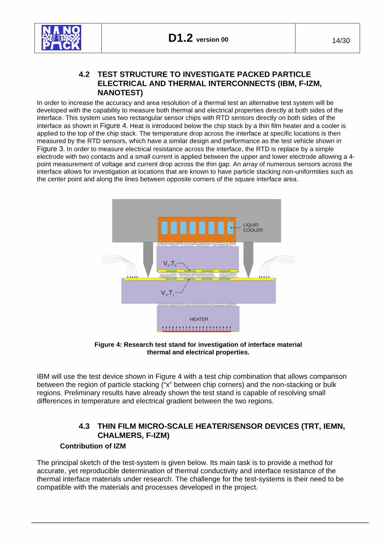
4.3 THIN FILM MICRO-SCALE HEATER/SENSOR DEVICES (TR T, IEMN, CHALMERS, F-IZM)
Contribution of IZM The principal sketch of the test-system is given below. Its main task is to provide a method for accurate, yet reproducible determination of thermal conductivity and interface resistance of the thermal interface materials under research. The challenge for the test-systems is their need to be compatible with the materials and processes developed in the project.
D1.2 version 00
15/30
Heat Spreader
DieNano-Interconnect forelectrical I/O
Integrated µ-thin-film sensor(WP 4)
Nano-filled adhesiveor nano-metal die-attach (WP 2)
Nano-enhanced/structured die surface (WP 3)
Heat Spreader
DieNano-Interconnect forelectrical I/O
Integrated µ-thin-film sensor(WP 4)
Nano-filled adhesiveor nano-metal die-attach (WP 2)
Nano-enhanced/structured die surface (WP 3)
Figure 5 : Technological possibilities for T-sensors, flow-sensors and heaters Requirements are:
• Very good temperature resolution as delta T across the TIM will be small (of the order of 0.1 K)
• Compatible with adhesives, greases and metal TIMs • Surface enhancement on Cu, Au finishes • Integration of heater and T-sensors and passivation • T-sensor structures that can also be used as flux sensors.
Therefore different technological processes could be eligible: Processing possibilities:
• Sputtering of seed layers (TiW, TiPt) • Application of sputtered or electroplated conductive metal layers (Au, CrNi, Al) • Structuring for redistribution (Litho) • Passivation layers (polymer, CVD Oxide, glass?) • Curing of polymers
ρ [10-6 Ωcm at RT]: Ag 1.6, Cu 1.7, Au 2.2, Al 2.7, Pt 11.0, Ni 7.0, CrNi 110α [10-3/K]: Ag 3.8, Cu 3.9, Au 4.0, Al 4.0, Pt 3.9, Ni 6.7, CrNi 0.14 ρ [10-6 Ωcm at RT]: Ag 1.6, Cu 1.7, Au 2.2, Al 2.7, Pt 11.0, Ni 7.0, CrNi 110α [10-3/K]: Ag 3.8, Cu 3.9, Au 4.0, Al 4.0, Pt 3.9, Ni 6.7, CrNi 0.14
Electrical conductivity and temperature coefficient Materials especially suited for T-sensors (or flow-sensors by sandwich structure) are Au or Al due to a very high sensitivity. Heater structures can be more effectively designed in CrNi. The first design of a test-system could look like the one given below. To make up for possible tilt of the die, the heat flow can be also measured by a small T-drop across a calibrated thin-film passivation layer. Four sensors (one in each corner) should suffice to obtain a position dependent flow through the sample. Temperature resolution should be high as the Si layers are thin and the temperature is monitored directly at the interface.
D1.2 version 00
16/30
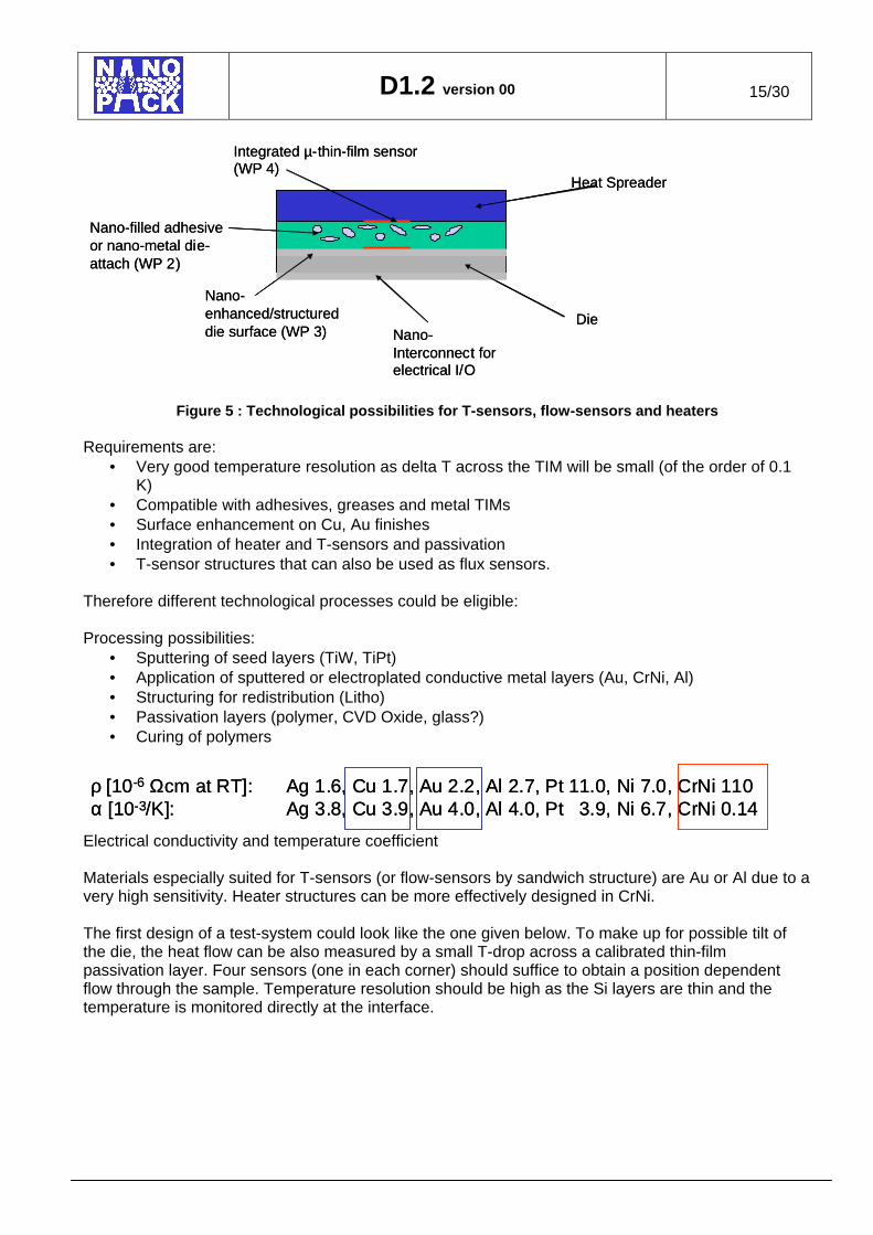
Cold Plate
Thin film heater
Si
Thin film T-sensor
Thin film j th- sensor made of 2 T-sensors separated bythin oxide, glass or polymer
a = 12 mm
top view with flowsensor
jth(x,y)
Cold Plate
Thin film heater
Si
Thin film T-sensor
Thin film j th- sensor made of 2 T-sensors separated bythin oxide, glass or polymer
a = 12 mm
top view with flowsensor
jth(x,y)
Figure 6 : Improved set-up with best temperature resolution
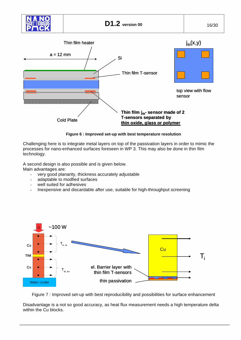
Challenging here is to integrate metal layers on top of the passivation layers in order to mimic the processes for nano-enhanced surfaces foreseen in WP 3. This may also be done in thin film technology. A second design is also possible and is given below. Main advantages are:
- very good planarity, thickness accurately adjustable - adaptable to modfied surfaces - well suited for adhesives - Inexpensive and discardable after use, suitable for high-throughput screening
Tt1 .. tn
Tb1 ..b n
Cu
Cu
TIM
Water cooler
Q ~100 W
Cu
Ti
el. Barrier layer withthin film T-sensors
thin passivation
Tt1 .. tn
Tb1 ..b n
Cu
Cu
TIM
Water cooler
Q ~100 W
Cu
Ti
el. Barrier layer withthin film T-sensors
thin passivation
Figure 7 : Improved set-up with best reproducibility and possibilities for surface enhancement
Disadvantage is a not so good accuracy, as heat flux measurement needs a high temperature delta within the Cu blocks.

D1.2 version 00
17/30
The Thinfilm Test Structure The heating structure could have 2 or 4 ports with high resistivity and low TCR, whereas the temperature sensors must have 4 ports for probing and should show a low resisitivity and high TCR.
Heater: - high resistivity- low temperature coefficient (TCR)
Temperature Sensor:- low resistivity- high temperature coefficient (TCR)
I+ I-I+ I-
I+ I-
U+ U-
I+ I-
U+ U-
Figure 8 : Possible structure for heater (2-point) and temperature sensors (4-point) Typical values for resistivity and TCR are given for some thinfilm metals. The material should also exhibit corrosion and oxidation resistance to minimize time and temperature dependet drifts.
Metal ρ TCRµΩcm 1/K
Ag 1,6 0,00380Cu 1,7 0,00390Au 2,2 0,00400Al 2,7 0,00400Pt 11 0,00390Ni 7 0,00670Cr 13 *
NiCr 110 0,00014
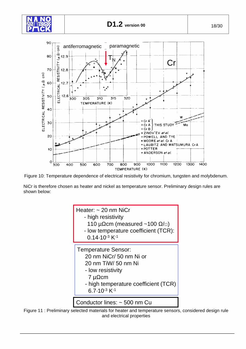
Figure 9 : Specific electrical resistivity ρ and temperature coefficient TCR for several metals Chromium has a non-linear TCR due to its Néel temperature around room temperature which occurs with the antiferromagnitic phase transformation.
D1.2 version 00
18/30
Cr
paramagneticantiferromagnetic
TN
Figure 10: Temperature dependence of electrical resistivity for chromium, tungsten and molybdenum. NiCr is therefore chosen as heater and nickel as temperature sensor. Preliminary design rules are shown below:
Heater: ~ 20 nm NiCr- high resistivity 110 µΩcm (measured ~100 Ω/)
- low temperature coefficient (TCR):0.14·10-3 K-1
Temperature Sensor: 20 nm NiCr/ 50 nm Ni or20 nm TiW/ 50 nm Ni- low resistivity7 µΩcm
- high temperature coefficient (TCR)6.7·10-3 K-1
Conductor lines: ~ 500 nm Cu
Figure 11 : Preliminary selected materials for heater and temperature sensors, considered design rule and electrical properties

D1.2 version 00
19/30
CVD oxideCuNi
TiWNiCr
minimal overlap:
10 µm10 µm 10 µm10 µm
Figure 12: Design schematic Silicon will be used as a substrate for the thinfilm processes. For the next steps we have to design the test chips. Therefore we need following informations to proceed: How the test chips will be used?, Chip size and thickness (standard: 670 µm)? Is there a specific back side metallization required to implement the chip into the test configuration?
substrate 1
substrate 2
TIM
test chip 2
test chip 1
wire bond encapsulation
substrate 1
substrate 2
TIM
test chip 2
test chip 1
wire bond encapsulation
Figure 13: Preliminary sketch of potential test setup
Heater: - one heating structure on chip only? - two electrical ports per heater?- heater on both sides, top & bottom?
Temperature Sensor:- how many T-sensors per test chip?- how should they be distributed?- one current line for all T-sensors?- 2 voltage sensors per T-sensor
I+ I-
I+I-
U+U-
I+ I-
U1+
U1- U2
+
U2-
1 2
Figure 14 : Schematic of heater and temperature sensor structures. Realization the interconnect scheme of test chips to outside should be realized? wire bonding? Flex substrate interconnect?
D1.2 version 00
20/30
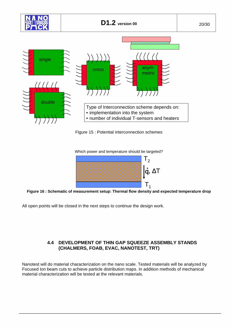
Type of Interconnection scheme depends on:• implementation into the system• number of individual T-sensors and heaters
single
double
cross asym-metric
Figure 15 : Potential interconnection schemes
Which power and temperature should be targeted?
q., ∆Tq.q., ∆T
T1
T2
Figure 16 : Schematic of measurement setup: Thermal flow density and expected temperature drop
All open points will be closed in the next steps to continue the design work.
4.4 DEVELOPMENT OF THIN GAP SQUEEZE ASSEMBLY STANDS (CHALMERS, FOAB, EVAC, NANOTEST, TRT)
Nanotest will do material characterization on the nano scale. Tested materials will be analyzed by Focused Ion beam cuts to achieve particle distribution maps. In addition methods of mechanical material characterization will be tested at the relevant materials.
D1.2 version 00
21/30
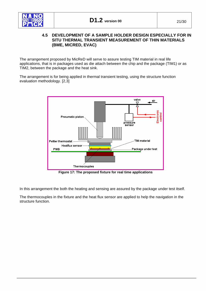
4.5 DEVELOPMENT OF A SAMPLE HOLDER DESIGN ESPECIALL Y FOR IN SITU THERMAL TRANSIENT MEASUREMENT OF THIN MATERIAL S (BME, MICRED, EVAC)
The arrangement proposed by MicReD will serve to assure testing TIM material in real life applications, that is in packages used as die attach between the chip and the package (TIM1) or as TIM2, between the package and the heat sink. The arrangement is for being applied in thermal transient testing, using the structure function evaluation methodology. [2,3]
Figure 17: The proposed fixture for real time applications
In this arrangement the both the heating and sensing are assured by the package under test itself.
The thermocouples in the fixture and the heat flux sensor are applied to help the navigation in the structure function.

D1.2 version 00
22/30
5 TEST VEHICLES USED AS FINAL DEMONSTRATORS IN WP7
5.1 THAV TEST VEHICLES THAT WILL BE USED FOR THE FI NAL EVALUATION IN WP7
Thales Avionics will test the TIM performance in the case of the cooling of an electronic card for the In Flight Entertainment Seat Equipment (IFE). The test vehicle will be a Seat Electronics Box (SEB). The SEB shall supply the passenger seats in the Cabin and beds/seats in the Rooms with audio, video, games, telephone, etc….
There shall be different SEB types corresponding to the required hardware, which is needed to accommodate the requested functions. The SEB type supporting all functions shall have the capability of supplying a minimum of three passenger seats, which necessary for a triple seat-group (may be reduced to two for double seat).
The demonstrator will be made from a SEB having the following sizes:
Length = 292mm, Width = 200mm and Thickness = 45mm The SEB contains 2 PCBs with dissipative components.
Figure 18 The final demonstrator used by Thales
PCB description
- Material: FR4, - Considering that the heat dissipation can reach 100 Watts, the PCB internal structure contains 2
copper layers of 35 µm thickness, - In order to improve conduction heat transfers from the PCB to the SEB, the PCB edges zones are
metallised and linked for one hand to the internal layers and for the other hand to the covers.
The SEB demonstrators are integrating 2 types of components:
PCBs
D1.2 version 00
23/30
Thermal chips, encapsulated in enhanced thermal packages and used for heat generation and temperature measurements (PMOS4),
Passive components (resistors TO220) for heat generation only.
Thermal chips The PMOS4 test chips, is a general purpose package performance monitoring test chip which contain test structures to evaluate the following IC package performance parameters: • Environmental reliability in terms of corrosion of on-chip metallization, • Thermo-mechanical reliability in terms of:
- stress induced resistance changes in silicon-based diffused resistors - stress induced metal shift in on chip metallization,
• Thermal resistance between the chip surface and some external reference temperature on the IC package, circuit board or the ambient air.
• Temperature of the component junction.
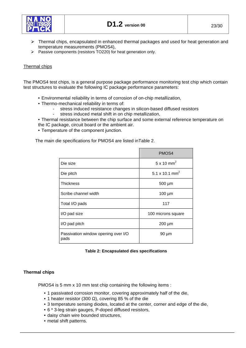
The main die specifications for PMOS4 are listed inTable 2.
PMOS4
Die size 5 x 10 mm2
Die pitch 5.1 x 10.1 mm2
Thickness 500 µm
Scribe channel width 100 µm
Total I/O pads 117
I/O pad size 100 microns square
I/O pad pitch 200 µm
Passivation window opening over I/O pads
90 µm
Table 2: Encapsulated dies specifications
Thermal chips
PMOS4 is 5 mm x 10 mm test chip containing the following items :
• 1 passivated corrosion monitor, covering approximately half of the die, • 1 heater resistor (300 Ω), covering 85 % of the die • 3 temperature sensing diodes, located at the center, corner and edge of the die, • 6 * 3-leg strain gauges, P-doped diffused resistors, • daisy chain wire bounded structures, • metal shift patterns.
D1.2 version 00
24/30
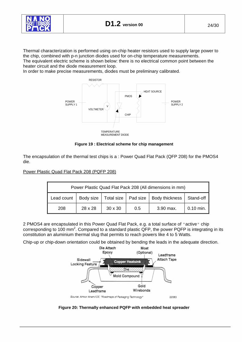
Thermal characterization is performed using on-chip heater resistors used to supply large power to the chip, combined with p-n junction diodes used for on-chip temperature measurements. The equivalent electric scheme is shown below: there is no electrical common point between the heater circuit and the diode measurement loop. In order to make precise measurements, diodes must be preliminary calibrated.
PMOS
CHIP
POWERSUPPLY 2
POWERSUPPLY 1
RESISTOR
VOLTMETER V
HEAT SOURCE
TEMPERATUREMEASUREMENT DIODE
Figure 19 : Electrical scheme for chip management
The encapsulation of the thermal test chips is a : Power Quad Flat Pack (QFP 208) for the PMOS4 die.
Power Plastic Quad Flat Pack 208 (PQFP 208)
Power Plastic Quad Flat Pack 208 (All dimensions in mm)
Lead count Body size Total size Pad size Body thickness Stand-off
208 28 x 28 30 x 30 0.5 3.90 max. 0.10 min.
2 PMOS4 are encapsulated in this Power Quad Flat Pack, e.g. a total surface of "active" chip corresponding to 100 mm2. Compared to a standard plastic QFP, the power PQFP is integrating in its constitution an aluminium thermal slug that permits to reach powers like 4 to 5 Watts.
Chip-up or chip-down orientation could be obtained by bending the leads in the adequate direction.
Figure 20: Thermally enhanced PQFP with embedded heat spreader

D1.2 version 00
25/30
Passive components: RT020 resistor RTO 20 resistors are used to produce the heat additionally to the thermal test components. They consist in a thick film surface mounted medium body with maximum power dissipation of 20 W each, supplied in TO-220 packages and implemented on the active side of the demonstrator PCB.
Figure 21: The RT020 resistor SEB Cooling methods There are several ways, depending of the thermal dissipated power, which can be used for the cooling of the SEB. In the case of low power, the cooling can be made with air natural convection. But if the power is too high, the cooling system must be improved using heat pipe (HP) or loop heat pipes systems (LHP) (see the following figure). Heat Pipe and Loop Heat Pipe are two phases heat transfer systems which allow to transfer heat between two points with a high efficiency. On the following figure, heat pipe allow to transport heat between the dissipating component and the SEB wall whereas Loop Heat Pipe extract the heat from the SEB wall to an external heat sink (not represented).
Figure 22: SEB cooling with Heat Pipes and Loop Heat Pipes
LHP Condenser
Heat Pipe Heat pipe
LHP Condenser
D1.2 version 00
26/30
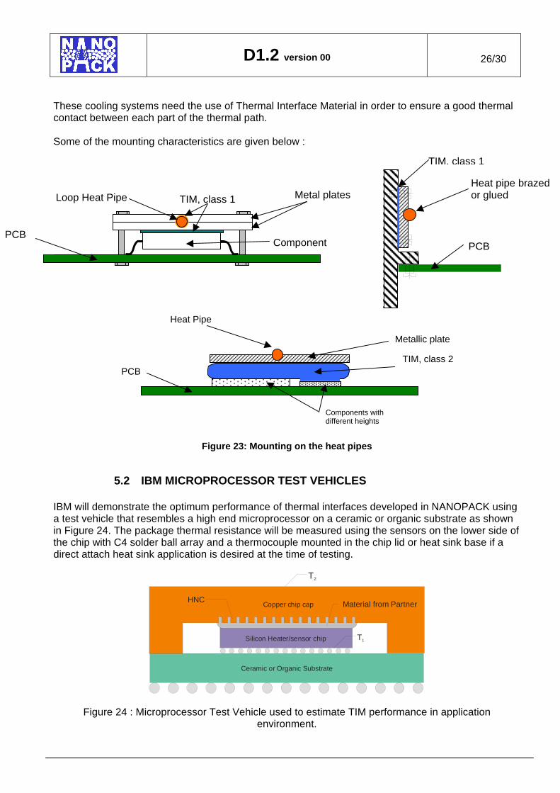
These cooling systems need the use of Thermal Interface Material in order to ensure a good thermal contact between each part of the thermal path. Some of the mounting characteristics are given below :
Figure 23: Mounting on the heat pipes
5.2 IBM MICROPROCESSOR TEST VEHICLES IBM will demonstrate the optimum performance of thermal interfaces developed in NANOPACK using a test vehicle that resembles a high end microprocessor on a ceramic or organic substrate as shown in Figure 24. The package thermal resistance will be measured using the sensors on the lower side of the chip with C4 solder ball array and a thermocouple mounted in the chip lid or heat sink base if a direct attach heat sink application is desired at the time of testing.
T1
T2
Material from PartnerHNC
Copper chip cap
Ceramic or Organic Substrate
Silicon Heater/sensor chip
Figure 24 : Microprocessor Test Vehicle used to estimate TIM performance in application environment.
Loop Heat Pipe
PCB Component
Metal plates TIM, class 1
Heat pipe brazed or glued
PCB
TIM, class 1
TIM, class 2
Components with different heights
PCB
Heat Pipe
Metallic plate

D1.2 version 00
27/30
5.3 BOSCH TEST VEHICLES THAT WILL BE USED FOR THE F INAL EVALUATION IN WP7
Bosch will test TIM performance by benchmarking thermal resistance of newly developed materials and processes against thermal performance of an existing product. We chose an electrical control unit with integrated high power circuits as given in the figure below.
Figure 25 : Electrical control unit with logic circuit (centre) and three surrounding power circuits The logic circuit in the centre of the control unit is based on LTTC substrate. TIM2 would have to be electrically isolating therefore. But, thermal loss of logic circuit is quite low and is not addressed in NanoPack, therefore. The surrounding power circuits are based on DBC (direct bonded copper substrate). As DBC provides electrical isolation between upper side and lower side, TIM2 does not need to be electrically isolating. We will test thermal performance of DBC substrate with 2 soldered diodes on top connected to a heat sink.
5.4 TRT TEST VEHICLE The RF-MEMS capacitive switch relies on a metal planar membrane suspended over the central line of coplanar waveguide, and resting on its ends on the ground lines. An electrode and a dielectric are integrated in the signal line. When a DC voltage is applied between this electrode and the metal membrane, this latter is deflected downwards due to electrostatic forces. In the un-actuated state, the membrane presents a high impedance with respect to the line, and the signal is unaffected. In the down position, the membrane is capacitively coupled to the bottom plane, and short-circuits the signal to the ground.
Figure 26: Non packaged RF-MEMS capacitive shunt switch
D1.2 version 00
28/30
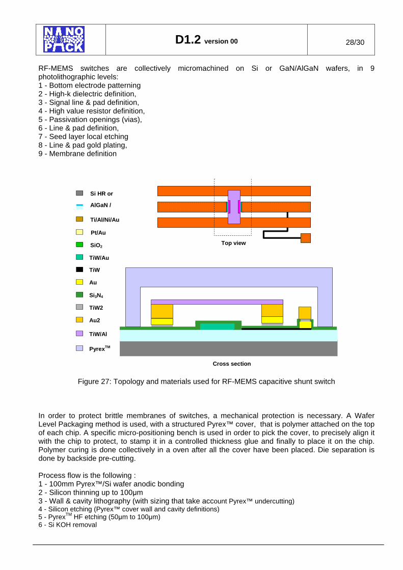
RF-MEMS switches are collectively micromachined on Si or GaN/AlGaN wafers, in 9 photolithographic levels: 1 - Bottom electrode patterning 2 - High-k dielectric definition, 3 - Signal line & pad definition, 4 - High value resistor definition, 5 - Passivation openings (vias), 6 - Line & pad definition, 7 - Seed layer local etching 8 - Line & pad gold plating, 9 - Membrane definition
Top view
Cross section
Si HR or SiC
Ti/Al/Ni/Au
AlGaN / GaN
SiO2
Pt/Au
TiW/Al
TiW/Au
Si3N4
TiW1Au 1
TiW2
Au2
Pyrex TM
Figure 27: Topology and materials used for RF-MEMS capacitive shunt switch
In order to protect brittle membranes of switches, a mechanical protection is necessary. A Wafer Level Packaging method is used, with a structured Pyrex™ cover, that is polymer attached on the top of each chip. A specific micro-positioning bench is used in order to pick the cover, to precisely align it with the chip to protect, to stamp it in a controlled thickness glue and finally to place it on the chip. Polymer curing is done collectively in a oven after all the cover have been placed. Die separation is done by backside pre-cutting. Process flow is the following : 1 - 100mm Pyrex™/Si wafer anodic bonding 2 - Silicon thinning up to 100µm 3 - Wall & cavity lithography (with sizing that take account Pyrex™ undercutting) 4 - Silicon etching (Pyrex™ cover wall and cavity definitions) 5 - PyrexTM HF etching (50µm to 100µm) 6 - Si KOH removal
D1.2 version 00
29/30
7 - Saw dicing (cover die separation)
Figure 28: Figure: Images of packaged RF-MEMS switches, before and after die separation
6 CONCLUSION This report has defined the test specimen and test system which will be used in WP4 (Design and fabrication of test structure) T0+6 -> T0+30. The objectives of WP4 are : To research, simulate, design and manufacture test structures to facilitate the measurement of
thin layers of very high thermal conductivity material. As different measurement methods will be used in the consortium, different test conditions have to be elaborated, examined, perfected and finally prepared for standardization
To develop test structures in order to investigate the electrical properties of micro scale particle stacks for application as electrical interconnects in stacked chip packages
WP4 will explore and manufacture test structures to facilitate the measurement of thin layers of very high thermal conductivity material. As different measurement methods will be used in the consortium different test conditions have to be elaborated, examined, perfected and finally prepared for standardization. WP4 will allow to characterize the thermal interface materials developed in WP2 and WP3 along with their process dependence in their thermal, electrical and thermo-mechanical properties.
D1.2 version 00
30/30
REFERENCES
1. D. L. Saums, et al: Challenges in thermal interface material testing. The 22nd Annual IEEE SEMI-THERM Symposium, 14-16 March, 2006, Dallas, TX, USA, pp. 42-49
2. V. Székely, Identification of RC Networks by Deconvolution: Chances and Limits, IEEE Transactions on Circuits and Systems-I. Theory and Applications, CAS-45 (3):244-258, 1998
3. Rencz M., Székely V.,: Measuring partial thermal resistances in a heat flow path, IEEE Transactions on CPT, Vol 25,No 4, Dec. 2002, pp 547-553


![[D1.2] Final child models. - hal.archives-ouvertes.fr](https://img.pdfslide.us/doc/110x75/62827de3cfaa80788828ba23/d12-final-child-models-halarchives-.jpg)