Embed Size (px)
Citation preview
Nanoscale
PAPER
Cite this: DOI: 10.1039/c4nr04387a
Received 1st August 2014,Accepted 29th October 2014
DOI: 10.1039/c4nr04387a
www.rsc.org/nanoscale
Cyclic chlorine trap-doping for transparent,conductive, thermally stable and damage-freegraphene†
Viet Phuong Pham,‡a Kyong Nam Kim,‡b Min Hwan Jeon,a Ki Seok Kimb andGeun Young Yeom*a,b
We propose a novel doping method of graphene using the cyclic trap-doping method with low energy
chlorine adsorption. Low energy chlorine adsorption for graphene chlorination avoided defect (D-band)
formation during the doping by maintaining the π-bonding of the graphene, which affects conductivity. In
addition, by trapping chlorine dopants between the graphene layers, the sheet resistance could be
decreased by ∼88% under optimized conditions. Among the reported doping methods, including chemi-
cal, plasma, and photochemical methods, the proposed doping method is believed to be the most prom-
ising for producing graphene with extremely high transmittance, low sheet resistance, high thermal
stability, and high flexibility for use in various flexible electronic devices. The results of Raman spec-
troscopy and sheet resistance showed that this method is also non-destructive and controllable. The
sheet resistance of the doped tri-layer graphene was 70 Ω per sq. at transmittance of 94%, and which was
maintained for more than 100 h in a vacuum at 230 °C. Moreover, the defect intensity of graphene was
not increased during the cyclic trap-doping.
Introduction
Graphene has attracted much attention owing to its remark-able mechanical and electrical properties and is being activelydeveloped to realize its full potential.1–7 Some of its importantproperties are suitable for making transparent conductivefilms: high conductivity, high transparency, and excellent flexi-bility; because of these superior properties, graphene has beenstudied as a possible replacement for indium tin oxide(ITO).9–11,13–15 Its serious disadvantages, however, have beenthe relatively high sheet resistance (∼a few hundred Ω per sq.)compared to that of ITO (a hundred Ω per sq.) under similaroptical transmittance conditions and the difficulty in scaling itto large size. With regard to the latter, many approaches andadvances have been reported for the synthesis of graphene bylarge area chemical vapor deposition (CVD).8–11,13–16 Theformer, i.e., the relatively high sheet resistance, has been abottleneck for its application to transparent conductive films.The sheet resistance of ideal graphene is much lower than that of
the CVD graphene reported.9 The higher sheet resistance ofCVD graphene originates from and is strongly dependent ondefects in the crystal, wrinkles, and the grain and domainsizes of the actually grown graphene layers. For these reasons,researchers have tried to improve the sheet resistance byvarious doping methods, including chemical,11,12,17
plasma,18–20 and photochemical methods.20 However, manyproblems still remain to be solved, such as the much highersheet resistance than that of ITO under similar optical trans-mittance conditions, the transmittance degradation duringchemical doping, the thermal instability and serious damageduring plasma doping, etc.
For example, in the case of wet chemical doping, Guneset al. showed the possibility of achieving low sheet resistanceby chemical doping, and obtained a sheet resistance of 54 Ωper sq. using four graphene layers.11 However, their dopingprocess showed the relatively poor transmittance of 85%because of the agglomeration of Au ions by the AuCl3 chemicalthey used. In addition to this process, various other chemicaldoping processes have also been investigated to improve thesheet resistance and transmittance.17,20–24 However, thesemethods did not satisfy both low sheet resistance and hightransmittance at the same time. As another technique, Li et al.tried to reduce the sheet resistance using the photochemicaldoping process.25 The sheet resistance they obtained, however,was significantly increased by about 3 orders of magnitude.
†Electronic supplementary information (ESI) available. See DOI: 10.1039/c4nr04387a‡These authors contributed equally to this work.
aSKKU Advanced Institute of Nano Technology (SAINT), Sungkyunkwan University
(SKKU), Suwon, Gyeonggi-do 440-746, Republic of Korea. E-mail: [email protected] of Advanced Materials Science and Engineering, Sungkyunkwan University
(SKKU), Suwon, Gyeonggi-do 440-746, Republic of Korea
This journal is © The Royal Society of Chemistry 2014 Nanoscale
Publ
ishe
d on
11
Nov
embe
r 20
14. D
ownl
oade
d by
Sun
gkyu
nkw
an U
nive
rsity
on
17/1
1/20
14 0
0:00
:04.
View Article OnlineView Journal
This result meant that the photochemical method interruptedthe conducting system of graphene, and introduced damage-inducing scattering centers.
In this study, we propose an innovative method for dopinggraphene to realize a graphene film with low sheet resistance,high transparency and high thermal stability while maintain-ing the nature of graphene. To realize a graphene film havingthese properties, we used the cyclic trap-doping method withlow energy chlorine adsorption. The graphene film synthesizedby chemical vapor deposition (CVD) was transferred to PETand quartz films for low energy chlorine doping. Our resultsdemonstrated that the graphene network was not destroyed bylow energy adsorption. The proposed method produced gra-phene films with a high transmittance of 94% at 550 nm and asheet resistance of 70 Ω per sq. with excellent thermal stabilityafter two cyclic chlorine trap-doping processes.
Results and discussion
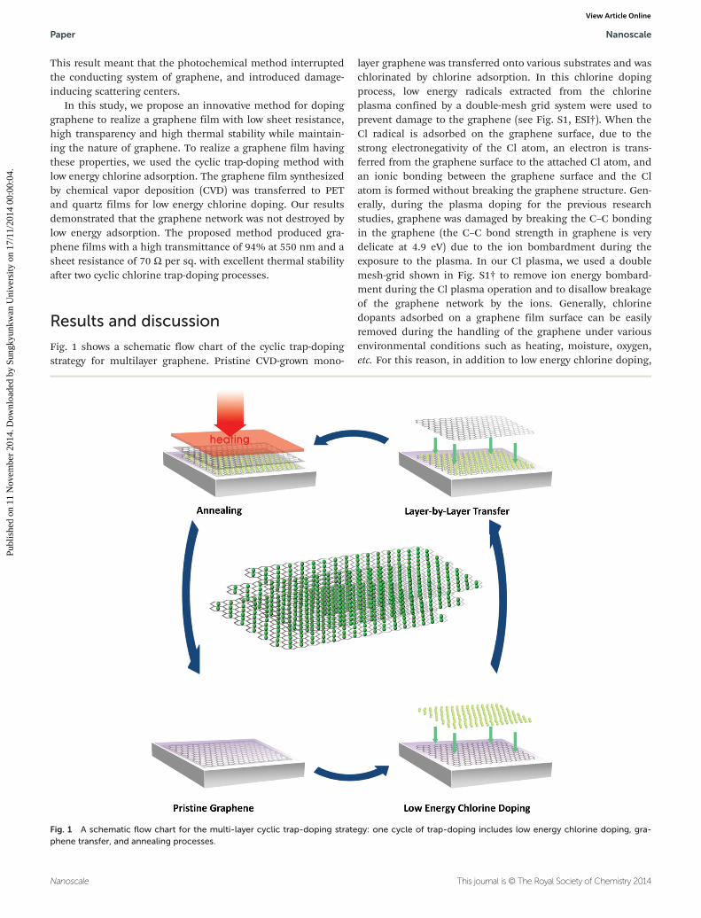
Fig. 1 shows a schematic flow chart of the cyclic trap-dopingstrategy for multilayer graphene. Pristine CVD-grown mono-
layer graphene was transferred onto various substrates and waschlorinated by chlorine adsorption. In this chlorine dopingprocess, low energy radicals extracted from the chlorineplasma confined by a double-mesh grid system were used toprevent damage to the graphene (see Fig. S1, ESI†). When theCl radical is adsorbed on the graphene surface, due to thestrong electronegativity of the Cl atom, an electron is trans-ferred from the graphene surface to the attached Cl atom, andan ionic bonding between the graphene surface and the Clatom is formed without breaking the graphene structure. Gen-erally, during the plasma doping for the previous researchstudies, graphene was damaged by breaking the C–C bondingin the graphene (the C–C bond strength in graphene is verydelicate at 4.9 eV) due to the ion bombardment during theexposure to the plasma. In our Cl plasma, we used a doublemesh-grid shown in Fig. S1† to remove ion energy bombard-ment during the Cl plasma operation and to disallow breakageof the graphene network by the ions. Generally, chlorinedopants adsorbed on a graphene film surface can be easilyremoved during the handling of the graphene under variousenvironmental conditions such as heating, moisture, oxygen,etc. For this reason, in addition to low energy chlorine doping,
Fig. 1 A schematic flow chart for the multi-layer cyclic trap-doping strategy: one cycle of trap-doping includes low energy chlorine doping, gra-phene transfer, and annealing processes.
Paper Nanoscale
Nanoscale This journal is © The Royal Society of Chemistry 2014
Publ
ishe
d on
11
Nov
embe
r 20
14. D
ownl
oade
d by
Sun
gkyu
nkw
an U
nive
rsity
on
17/1
1/20
14 0
0:00
:04.
View Article Online

the method of confining chlorine dopants between graphenefilms by transfer of a second graphene layer on the doped gra-phene layer has been used for the bi-layer doped graphene.For the tri-layer doped graphene, after the transfer of thesecond layer, chlorine doping was repeated on the second gra-phene layer, followed by the transfer of the third graphenelayer on top of the second graphene layer, etc. Therefore,through the cyclic low energy chlorine doping and transferstrategy, multi-layer doped graphene can be prepared. Duringcyclic chlorine radical doping, just after the transfer of eachgraphene layer, the graphene was annealed in a vacuumfurnace at 250 °C for the SiO2 and quartz substrates, and at230 °C for the PET film for 30 min.26
To understand the effect of chlorine doping by low energychlorine adsorption using chlorine plasma, a Raman analysiswas carried out. The doping effect can be observed throughthe changes in the peak positions of the G and 2D bands.Fig. 2(a) shows the Raman spectra data for a mono-layer gra-phene sample before and after the chlorine doping processusing low energy chlorine radicals for 25 s and after heating ina vacuum furnace at 230 °C for 6.5 h. Fig. 2(b) and (c) are thezoom-in spectra of the Raman G and 2D peaks shown in Fig. 2(a),
respectively. The chlorine plasma was generated at 20 W of rfpower with 60 sccm 10 mTorr Cl2. From previous researchstudies, it is found that, in the case of conventional plasmadoping techniques, serious defects are generally formed in thegraphene network because the energetic ions and electrons inthe plasma bombard the graphene surface and destroy the sp2
bonded carbon network of graphene. As the characteristic dis-order-induced D band emerges, the 2D band intensity isdecreased significantly and the G band is also broad-ened18,27,28 (see Fig. S2, ESI†). The damage and severe degra-dation of the graphene film by these methods significantlylimit the application of the graphene film to various electronicdevices. As shown in Fig. 2(a), after chlorine radical dopingwith low energy chlorine radicals, the D peak intensity of gra-phene did not increase, indicating that there was no noticeabledegradation of graphene after the doping even though theID/IG ratio was slightly increased from 0.07 to 0.09. However, asshown in Fig. 2(b) and (c), G and 2D peak positions were blue-shifted by 5 cm−1 and 7 cm−1, respectively. We heated thedoped graphene in a vacuum furnace at 230–250 °C for 100 hand checked its reversibility through the Raman shift. If thisdoping method does not affect the graphene network, then
Fig. 2 (a) Raman spectra data for a monolayer graphene sample before and after the chlorine doping process using the low energy chlorine radi-cals, and after heating at 230–250 °C for 6.5 h. The chlorine plasma was generated at 20 W of rf power with 60 sccm 10 mTorr Cl2. (b) Zoom-inspectrum of the Raman G peak before/after chlorine doping and after heating at 230–250 °C for 6.5 h. (c) Zoom-in spectrum of the Raman 2D peakbefore/after chlorine doping and after heating at 230–250 °C for 6.5 h. (d) XPS C 1s spectra of the pristine monolayer graphene and chlorine dopedmono-layer graphene after annealing at 230–250 °C for 6.5 h.
Nanoscale Paper
This journal is © The Royal Society of Chemistry 2014 Nanoscale
Publ
ishe
d on
11
Nov
embe
r 20
14. D
ownl
oade
d by
Sun
gkyu
nkw
an U
nive
rsity
on
17/1
1/20
14 0
0:00
:04.
View Article Online

after the removal of dopants through heating, the doped gra-phene should change back to pristine graphene. As shown inthe figures, after heating in a vacuum furnace at 230–250 °Cfor 100 h, the Raman shifts of G and 2D peaks by chlorinedoping returned back to their original positions, indicatingthat there was no damage to the graphene during doping bythe low energy chlorine doping method. Fig. 2(d) shows theX-ray photoelectron spectroscopy (XPS) C 1s narrow scanspectra of the pristine mono-layer graphene, chlorine dopedmono-layer graphene and after heating in a vacuum furnace at230–250 °C for 100 h. In the chlorine doped mono-layer gra-phene sample, a C–Cl bonding peak at 286.8 eV due to chlor-ine doping on the graphene surface and a C–O bonding peakat 289 eV attributed to the presence of carbon oxide contami-nations were observed. However, after heating, the C–Clbonding peak was significantly removed and recovered close tothat of the pristine mono-layer graphene. From these consist-ent results, the method of chlorine doping through low energychlorine adsorption is believed to be an effective method fordamage-free graphene doping. Therefore, we proceeded toinvestigate the chlorine trapping between the graphene layersoverlapping with each other in order to eliminate the abovedrawbacks as illustrated in Fig. 3.
In fact, for damage-free graphene doping, the plasma con-ditions need to be optimized such that high energy chlorineions do not bombard the graphene surface. Using low energychlorine radicals, we carried out doping experiments withmono-layer graphene and observed the variation in sheetresistance according to the beam conditions (see Fig. S3,ESI†). In low energy radical doping using chlorine plasma withthe double-mesh grid system, the number of chlorine radicalspassing through the mesh grid depends on the operation con-ditions such as rf power, plasma exposure time, etc. Theincrease of rf power increases not only the chlorine radicaldensity in the plasma but also the possibility of damaging thegraphene by increased high energy ion bombardment. Theincrease of the plasma exposure time increases the chlorineradical dose to the graphene. From these results, the chlorineplasma with the double-mesh grid could be used to controland optimize the degree of doping without damaging the gra-phene film. Under optimized conditions, the sheet resistanceof the graphene was decreased by more than 50% compared tothat of the pristine monolayer graphene film.
Generally, the effect of chlorine radical doping throughpure chemisorption accompanied by the breaking of the sp2
C–C bonding followed by the formation of C–Cl bonding canbe maintained for a longer time than that of chlorine radicaldoping through the physisorption of Cl on C–C bonding.However, by chlorine radical doping through pure chemisorp-tion, the graphene structure is damaged and sheet resistanceis increased by 3 orders of magnitude.20 This highly resistivegraphene film cannot be applied to various electronic appli-cations including transparent conductive films. On the otherhand, in the case of chlorine radical doping through physi-sorption, chlorine atoms are weakly bonded to the graphenesurface; therefore, it is difficult to maintain the doping effect
for a long time. For this reason, we trapped the chlorineradical dopants between the graphene layers using the trap-doping technique and studied the effect of trap-doping on thethermal stability and sheet resistance of the graphene struc-ture. Fig. 3(a) shows the changes of sheet resistance withheating time after the surface chlorine radical doping ofmono-layer graphene and that after the chlorine trap-dopingin a bi-layer graphene structure, which includes chlorinedoping and trapping between two graphene layers. The chlor-ine radical doping conditions were the same as thosedescribed in Fig. 2 and the graphene was heated in a vacuumfurnace at 230 °C for 30 min to 6.5 h to investigate the thermalstability of the doped graphene. As shown in the figure, for themono-layer graphene, after the surface chlorine radicaldoping, the sheet resistance became 50% of that of pristinegraphene. However, after the doped monolayer graphene washeated in a vacuum furnace at 230 °C for 100 h, the sheet
Fig. 3 (a) The changes of sheet resistance with heating time aftersurface chlorine radical doping of monolayer graphene and after chlor-ine trap-doping in a bilayer graphene. The chlorine radical doping con-ditions were the same as those described in Fig. 2 and the heating ofgraphene was conducted in a vacuum furnace at 230 °C for 30 min to100 h. (b) The change of sheet resistance through the cyclic trap-dopingwhich includes 1st cycle of trap-doping (chlorine doping, transfer of the2nd graphene layer, annealing) and 2nd cycle of trap-doping (2nd cycle ofchlorine doping, transfer of the 3rd graphene layer, annealing). Theannealing was also conducted at 230 °C in a vacuum furnace.
Paper Nanoscale
Nanoscale This journal is © The Royal Society of Chemistry 2014
Publ
ishe
d on
11
Nov
embe
r 20
14. D
ownl
oade
d by
Sun
gkyu
nkw
an U
nive
rsity
on
17/1
1/20
14 0
0:00
:04.
View Article Online

resistance returned to the level of the pristine graphenebecause the volatile chlorine dopants were removed from thesurface of the graphene film during the heating. However, inthe case of the trap-doped bi-layer graphene structure, thesheet resistance further decreased after heating for 30 min anddid not change significantly with increasing heating time upto 6.5 h. Therefore, the trap-doped bi-layer graphene structureremained stable after the doping.
In addition, as shown in Fig. 3(b), through the cyclic trap-doping, which includes the 1st cycle of trap-doping (chlorinedoping, transfer of the 2nd graphene layer, annealing), 2nd
cycle of trap-doping (2nd cycle of chlorine doping, transfer ofthe 3rd graphene layer, annealing), etc., the sheet resistance ofthe tri-layer graphene structure decreased significantly toabout 70 Ω per sq. The annealing was also conducted at230 °C for 30 min in a vacuum furnace. The significantly lowsheet resistance of a tri-layer graphene is related to the dopingeffect, which incidentally does not form any scattering centersin the graphene layers because chlorine doping through physi-sorption does not interrupt the conjugated system of the gra-phene composed of conducting π-bonds (see Fig. S4, ESI†). Inaddition to the low energy chlorine radical doping itself, theoptimization of the annealing condition after the trap-dopingwill play an important role in the decrease of the sheet resist-ance because in our results, the sheet resistance was furtherdecreased by about 40% and 14% after the annealing of 1st
and 2nd trap-doping, respectively. These decreases are believedto arise from the annealing of the defects in the graphenelayers with chlorine radicals trapped between the graphenelayers. Finally, the result shows that the trap doping method isvery stable and can be used as a damage-free graphene dopingmethod in combination with the low energy chlorine radicaldoping used for the mono-layer graphene.
Using transmission electron microscopy (TEM), the locationof chlorine atoms in the chlorine trap-doped graphene wasinvestigated. Fig. 4(a) and (b) show low-magnification color-scaled DF (dark field)-TEM images of a bi-layer graphene
without (pristine) and with the chlorine trap doping processusing the low energy radicals, respectively. Wide brown coloredareas in Fig. 4(b) are believed to be related to the locations ofchlorine atoms between the graphene layers caused by the trapdoping of chlorine. A thin network of brown color is alsoshown in Fig. 4(a) and, even though it is not clear this time, itis believed to be from the slight doping of Cl on the graphenefrom a FeCl3 etchant used during the graphene transferprocess (see the Experimental section). The existence of Clatoms in the brown colored area was confirmed throughmicro-EDS (energy dispersive X-ray spectroscopy) in TEM (seeFig. S5, ESI†).
Fig. 5 shows the optical transmittance of the mono-layerand tri-layer chlorine doped graphene on PET substrates. The
Fig. 4 Low-magnification DF-TEM images of a bi-layer graphene with/without trap doping. (a) DF-TEM image of pristine bi-layer graphene and (b)DF-TEM image after the chlorine trap-doping in a bilayer graphene. The chlorine radical doping conditions were the same as those described inFig. 2. The wide brown color areas in (b) are related to the chlorine atoms between the graphene layers.
Fig. 5 The optical transmittance measured using UV-Vis-NIR spec-troscopy for the PET substrate itself and the doped graphene on PETsubstrates with mono-, bi-, and tri-layer graphenes. White paper is thearea without any PET film.
Nanoscale Paper
This journal is © The Royal Society of Chemistry 2014 Nanoscale
Publ
ishe
d on
11
Nov
embe
r 20
14. D
ownl
oade
d by
Sun
gkyu
nkw
an U
nive
rsity
on
17/1
1/20
14 0
0:00
:04.
View Article Online
pristine mono-layer graphene showed a high transmittance of∼97.6% (±0.3%) at 550 nm. After the chlorine radical doping,although the sheet resistance was decreased by 50%, the trans-mittance remained the same as that of the pristine graphene.As the chlorine doping was repeated to tri-layer by cyclic trap-doping, the transmittance changed to ∼94%. This indicatesthat chlorine trap-doping did not deteriorate the optical trans-mittance, but only reduced the optical absorption when thegraphene film layer is increased to tri-layer.
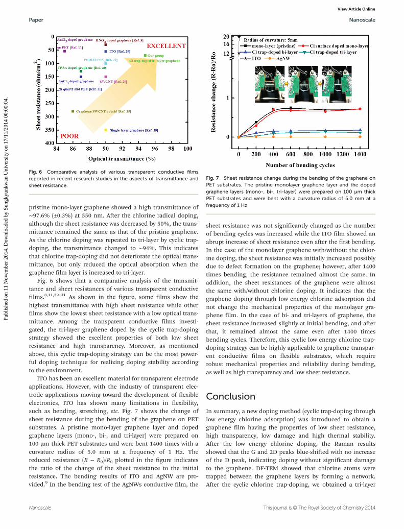
Fig. 6 shows that a comparative analysis of the transmit-tance and sheet resistances of various transparent conductivefilms.8,11,29–31 As shown in the figure, some films show thehighest transmittance with high sheet resistance while otherfilms show the lowest sheet resistance with a low optical trans-mittance. Among the transparent conductive films investi-gated, the tri-layer graphene doped by the cyclic trap-dopingstrategy showed the excellent properties of both low sheetresistance and high transparency. Moreover, as mentionedabove, this cyclic trap-doping strategy can be the most power-ful doping technique for realizing doping stability accordingto the environment.
ITO has been an excellent material for transparent electrodeapplications. However, with the industry of transparent elec-trode applications moving toward the development of flexibleelectronics, ITO has shown many limitations in flexibility,such as bending, stretching, etc. Fig. 7 shows the change ofsheet resistance during the bending of the graphene on PETsubstrates. A pristine mono-layer graphene layer and dopedgraphene layers (mono-, bi-, and tri-layer) were prepared on100 µm thick PET substrates and were bent 1400 times with acurvature radius of 5.0 mm at a frequency of 1 Hz. Thereduced resistance (R − R0)/R0 plotted in the figure indicatesthe ratio of the change of the sheet resistance to the initialresistance. The bending results of ITO and AgNW are pro-vided.9 In the bending test of the AgNWs conductive film, the
sheet resistance was not significantly changed as the numberof bending cycles was increased while the ITO film showed anabrupt increase of sheet resistance even after the first bending.In the case of the monolayer graphene with/without the chlor-ine doping, the sheet resistance was initially increased possiblydue to defect formation on the graphene; however, after 1400times bending, the resistance remained almost the same. Inaddition, the sheet resistances of the graphene were almostthe same with/without chlorine doping. It indicates that thegraphene doping through low energy chlorine adsorption didnot change the mechanical properties of the monolayer gra-phene film. In the case of bi- and tri-layers of graphene, thesheet resistance increased slightly at initial bending, and afterthat, it remained almost the same even after 1400 timesbending cycles. Therefore, this cyclic low energy chlorine trap-doping strategy can be highly applicable to graphene transpar-ent conductive films on flexible substrates, which requirerobust mechanical properties and reliability during bending,as well as high transparency and low sheet resistance.
Conclusion
In summary, a new doping method (cyclic trap-doping throughlow energy chlorine adsorption) was introduced to obtain agraphene film having the properties of low sheet resistance,high transparency, low damage and high thermal stability.After the low energy chlorine doping, the Raman resultsshowed that the G and 2D peaks blue-shifted with no increaseof the D peak, indicating doping without significant damageto the graphene. DF-TEM showed that chlorine atoms weretrapped between the graphene layers by forming a network.After the cyclic chlorine trap-doping, we obtained a tri-layer
Fig. 6 Comparative analysis of various transparent conductive filmsreported in recent research studies in the aspects of transmittance andsheet resistance.
Fig. 7 Sheet resistance change during the bending of the graphene onPET substrates. The pristine monolayer graphene layer and the dopedgraphene layers (mono-, bi-, tri-layer) were prepared on 100 µm thickPET substrates and were bent with a curvature radius of 5.0 mm at afrequency of 1 Hz.
Paper Nanoscale
Nanoscale This journal is © The Royal Society of Chemistry 2014
Publ
ishe
d on
11
Nov
embe
r 20
14. D
ownl
oade
d by
Sun
gkyu
nkw
an U
nive
rsity
on
17/1
1/20
14 0
0:00
:04.
View Article Online
graphene-based PET film with a sheet resistance of 70 Ω persq. at a transmittance of 94% at 550 nm. This means that thistrap-doping through low energy chlorine adsorption can be aneffective and controllable way to engineer the physical andelectronic properties of graphene. The observed results on thesheet resistance and transmittance were improved beyondother previous results. Especially, if the thermal stability isconsidered additionally, this doping method could be a power-ful technique. The graphene film doped by cyclic chlorinetrap-doping also showed excellent flexibility and stability inthe bending test. The cyclic chlorine trap-doping strategy intro-duced in this study can be applied to graphene used in variouselectronic applications such as printed electronics, flexibletouch screens, transistors, integrated circuits, etc.
Experimental sectionSynthesis of the graphene layer
Monolayer graphene films were synthesized on Cu foil by thechemical vapor deposition (CVD) method. Cu foil of 100 ×90 cm2 area and 75 µm thickness was placed in a vacuum CVDquartz chamber. The temperature was increased up to 1050 °Cin H2, 10 sccm, and the foil was annealed for 1 h at this temp-erature prior to growth. Graphene was synthesized at 1050 °Cby gas flow of H2/CH4, 10/20 sccm, for 30 min, and then thechamber was cooled down to room temperature with H2 gas,10 sccm, in 1 h. After the synthesis, the Cu foil was cut intosmall equal pieces (3 × 3 cm2), coated with poly(methyl metha-crylate) (PMMA), and immersed in a Cu etchant (FeCl3) solu-tion to etch away the Cu foil. When Cu was completely etchedaway, the graphene sheets with PMMA were rinsed in de-ionized water several times to wash away etchant residues.Then, PMMA-coated graphene sheets were transferred ontopolyethylene terephthalate (PET), quartz and SiO2 substrates.PMMA was removed with acetone for 30 min after the gra-phene had completely adhered to the substrates.
Cyclic trap-doping by low energy chlorine absorption andannealing (heating) procedure
The chlorine doping steps were repeated on the same gra-phene-coated substrate in order to maintain the cyclic chlorinetrap-doping of the graphene sheets up to tri-layers. One cycleof trap-doping includes low energy chlorine doping on the topof the graphene, trapping of chlorine by the transfer of anadditional graphene layer, and annealing at 250 °C for theSiO2 and quartz substrates, and at 230 °C for the PET film for30 min–6.5 h. The low energy chlorine doping was conductedwith the inductively coupled plasma (ICP) system with adouble-mesh grid shown in Fig. S1† using 10 mTorr 60 sccmCl2 at 20–300 W 13.56 MHz rf power. To minimize theadsorbed Cl dopant removal on the doped graphene surfaceduring the transfer of the second or third graphene layers onthe substrates with the doped graphene, the substrate withdoped graphene was not dipped in the deionized (DI) waterdirectly during the graphene transfer. Instead, the graphene
was transferred on PET film first and the graphene on the PETfilm was transferred to the substrate with doped graphene.However, as shown in Fig. S6,† the fabricated doped grapheneturned out to be extremely stable even for air exposure formore than 120 days, followed by DI water dipping for 3 hours,and followed by acetone cleaning for two hours. For the inves-tigation of the thermal stability, the prepared graphene filmswere also heated at around 230–250 °C for 100 h in a vacuumfurnace.
Characterization
Sheet resistance was measured using a sheet resistance meter(Dasoleng, FPP-2400) at room temperature for the graphenefilms on SiO2 and PET. Ultraviolet-visible-near infrared(UV-Vis-NIR) absorption spectroscopy (Shimadzu, 3600) andRaman spectroscopy (Renishaw, RM-1000 Invia) with an exci-tation energy of 2.41 eV (514 nm, Ar+ ion laser) were used tocharacterize the optical properties of the graphene films onthe PET, quartz and SiO2 substrates, respectively. For theobservation of chlorine atom locations between the graphenelayers prepared with/without the chlorine trapped doping,DF-TEM was used, and micro-EDS (energy dispersive X-rayspectroscopy) installed in the TEM was used for the analysis ofcomponents in Cl trapped area for a chlorine trap doped bi-layer graphene. The graphene surface was investigated usingangle resolved X-ray photoelectron spectroscopy (ARXPS,ESCA2000, VG Microtech Inc.) using an Mg Kα twin-anodesource. To observe the carbon binding states near the surface,the take-off angle was fixed at 45°. The bending test of the gra-phene coated on PET was carried out under the bending con-ditions of a curvature radius of 5.0 mm and a bendingfrequency of 1 Hz using an in-house bending test machine.
Acknowledgements
This research was supported by Nano Material TechnologyDevelopment Program through the National Research Foun-dation of Korea (NRF) funded by the Ministry of Education,Science and Technology (2012M3A7B4035323), and was alsosupported by the MOTIE (Ministry of Trade, Industry & Energy)(10048504) and KSRC (Korea Semiconductor Research Consor-tium) support program for the development of the future semi-conductor device.
Notes and references
1 K. S. Novoselov, A. K. Geim, S. V. Morozov, Y. Zhang,S. V. Dubonos, I. V. Grigorieva and A. A. Firsov, Science,2004, 306, 666–669.
2 K. S. Novoselov, A. K. Geim, S. V. Morozov, D. Jiang,M. I. Katsnelson, I. V. Grigorieva, S. V. Dubonos andA. A. Firsov, Nature, 2005, 438, 197–200.
3 C. R. Dean, A. F. Young, C. Lee, L. Wang, S. Sorgenfrei,K. Watanabe, T. Taniguchi, P. Kim, K. L. Shepard andJ. Hone, Nat. Nanotechnol., 2010, 5, 722–726.
Nanoscale Paper
This journal is © The Royal Society of Chemistry 2014 Nanoscale
Publ
ishe
d on
11
Nov
embe
r 20
14. D
ownl
oade
d by
Sun
gkyu
nkw
an U
nive
rsity
on
17/1
1/20
14 0
0:00
:04.
View Article Online

4 F. Wang, Y. B. Zhang, C. Tian, C. Girit, A. Zettl,M. Crommie and Y. R. Shen, Science, 2008, 320, 206–209.
5 N. O. Weiss, H. L. Zhou, L. Liao, Y. Liu, S. Jiang, Y. Huangand X. F. Duan, Adv. Mater., 2012, 24, 5782–5825.
6 A. K. Geim, Science, 2009, 324, 1530–1534.7 A. K. Geim and K. S. Novoselov, Nat. Mater., 2007, 6, 183–191.8 S. K. Bae, H. K. Kim, Y. B. Lee, X. F. Yu, J. S. Park, Y. Zheng,
J. Balakrishnan, T. Lei, H. R. Kim, Y. I. Song, Y. J. Kim,K. S. Kim, B. Ozyilmaz, J. H. Ahn, B. H. Hong and S. Iijima,Nat. Nanotechnol., 2010, 5, 574–578.
9 D. Langley, G. Giusti, C. Mayousse, C. Celle, D. Bellet andJ. P. Simonato, Nanotechnology, 2013, 24, 452001.
10 C. Mattevi, H. W. Kim and M. Chhowalla, J. Mater. Chem.,2011, 21, 3324–3334.
11 F. Gunes, H. J. Shin, C. Biswas, G. H. Han, E. S. Kim,S. J. Chae, J. Y. Choi and Y. H. Lee, ACS Nano, 2010, 4,4595–4600.
12 J. Zheng, H. T. Liu, B. Wu, C. A. Di, Y. L. Guo, T. Wu, G. Yu,Y. Q. Liu and D. B. Zhu, Sci. Rep., 2012, 2, 662.
13 U. N. Maiti, W. J. Lee, J. M. Lee, Y. T. Oh, J. Y. Kim,J. E. Kim, J. W. Shim, T. H. Han and S. O. Kim, Adv. Mater.,2014, 26, 40–67.
14 D. S. Hecht, L. B. Hu and G. Irvin, Adv. Mater., 2011, 23,1482–1513.
15 X. Huang, C. L. Tan, Z. Yin and H. Zhang, Adv. Mater.,2014, 26, 2185–2204.
16 M. Wang, S. K. Jang, W. J. Jang, M. W. Kim, S. Y. Park,S. W. Kim, S. J. Kahng, J. Y. Choi, R. S. Rouff, Y. J. Song andS. J. Lee, Adv. Mater., 2013, 25, 2746–2752.
17 H. Liu, Y. Liu and D. Zhu, J. Mater. Chem., 2011, 21, 3335–3345.
18 X. Zhang, A. Hsu, H. Wang, Y. Song, J. Kong,M. S. Dresselhaus and T. Palacios, ACS Nano, 2013, 7,7262–7270.
19 J. Wu, L. Xie, Y. G. Li, H. L. Wang, Y. Ouyang, J. Guo andH. Dai, J. Am. Chem. Soc., 2011, 13, 19668–19671.
20 Q. Zheng, Z. Li, J. Yang and J. K. Kim, Prog. Mater. Sci.,2014, 64, 200–247.
21 Y. Wang, C. Di, Y. Liu, H. Kajiura, S. Ye, L. Cao, D. Wei,H. Zhang, Y. Li and K. Noda, Adv. Mater., 2008, 20, 4442–4449.
22 Q. B. Zheng, M. M. Gudarzi, S. J. Wang, Y. Geng, Z. Li andJ.-K. Kim, Carbon, 2011, 49, 2905–2916.
23 P. Barpanda, G. Fanchini and G. G. Amatucci, Carbon,2011, 49, 2538–2548.
24 Q. Zheng, W. H. Ip, X. Lin, N. Yousefi, K. K. Yeung, Z. Liand J. K. Kim, ACS Nano, 2011, 7, 6039–6051.
25 B. Li, L. Zhou, D. Wu, H. Peng, K. Yan and Z. F. Liu, ACSNano, 2011, 5, 5957–5961.
26 Y. C. Lin, C. C. Lu, C. H. Yeh, C. H. Jin, K. Suenaga andP. W. Chiu, Nano Lett., 2012, 12, 414–419.
27 M. W. Iqbal, A. K. Singh, M. Z. Iqbal and J. H. Eom,J. Phys.: Condens. Matter, 2012, 24, 335301.
28 Z. Ni, Y. Wang and Z. Shen, Nano Res., 2008, 1, 273–291.
29 Y. Zhu, D. K. James and J. M. Tour, Adv. Mater., 2012, 24,4924–4955.
30 S. Tongay, K. Berke, M. Lemaitre, Z. Nasrollahi, D. B. Tanner,A. F. Hebard and B. R. Appleton, Nanotechnology, 2011, 22,425701.
31 K. K. Kim, A. Reina, Y. Shi, H. Park, L. J. Li, Y. H. Lee andJ. Kong, Nanotechnology, 2010, 21, 285205.
Paper Nanoscale
Nanoscale This journal is © The Royal Society of Chemistry 2014
Publ
ishe
d on
11
Nov
embe
r 20
14. D
ownl
oade
d by
Sun
gkyu
nkw
an U
nive
rsity
on
17/1
1/20
14 0
0:00
:04.
View Article Online

![[Unlocked]2 Engineer Wale (ways Experi1ttetlL Station ( WES ) ICE-QUAL-W2j CWQUA1>W2 WORKING REPORT 023 REPORT CALS CALS CALS XML 7— Title [Unlocked]](https://img.pdfslide.us/doc/110x75/60eab5e1d284cc7d816c9464/unlocked-2-engineer-wale-ways-experi1ttetll-station-wes-ice-qual-w2j-cwqua1w2.jpg)