Embed Size (px)
Citation preview
CY7C65632, CY7C65634
HX2VL™ Very Low Power USB 2.0Hub Controller
Cypress Semiconductor Corporation • 198 Champion Court • San Jose, CA 95134-1709 • 408-943-2600Document Number: 001-67568 Rev. *J Revised December 7, 2016
HX2VL™ Very Low Power USB 2.0 Hub Controller
Features
■ High performance, low-power USB 2.0 Hub, optimized for lowcost designs with minimum Bill-of-material
■ USB 2.0 hub controller❐ Compliant with USB 2.0 specification, TID# 30000060❐ Up to four downstream ports support❐ Downstream ports are backward compatible with FS, LS❐ Single transaction translator (TT) for low cost
■ Very low power consumption ❐ Supports bus-powered and self-powered modes❐ Auto switching between bus-powered and self-powered❐ Single MCU with 2K ROM and 64 byte RAM❐ Lowest power consumption
■ Highly integrated solution for reduced BOM cost❐ Internal regulator – single power supply 5 V required❐ Provision of connecting 3.3 V with external regulator❐ Integrated upstream pull-up resistor❐ Integrated pull-down resistors for all downstream ports❐ Integrated upstream/downstream termination resistors❐ Integrated port status indicator control
❐ 12 MHz +/– 500 ppm external crystal with drive level 600 µW(integrated PLL) clock input with optional 27/48 MHzoscillator clock input
❐ Internal power failure detection for ESD recovery
■ Downstream port management❐ Support individual and ganged mode power management❐ Overcurrent detection❐ Two port status indicators per downstream port
■ Maximum configurability❐ VID and PID are configurable through external EEPROM❐ Number of ports, removable/non-removable ports are
configurable through EEPROM and I/O pin configuration❐ I/O pins can configure gang/individual mode power
switching, reference clock source and polarity of powerswitch enable pin
❐ Configuration options also available through mask ROM
■ Available in space saving 48-pin (7 × 7 mm) TQFP and 28-pin(5 × 5 mm) QFN packages
■ Supports 0 °C to 70 °C temperature range
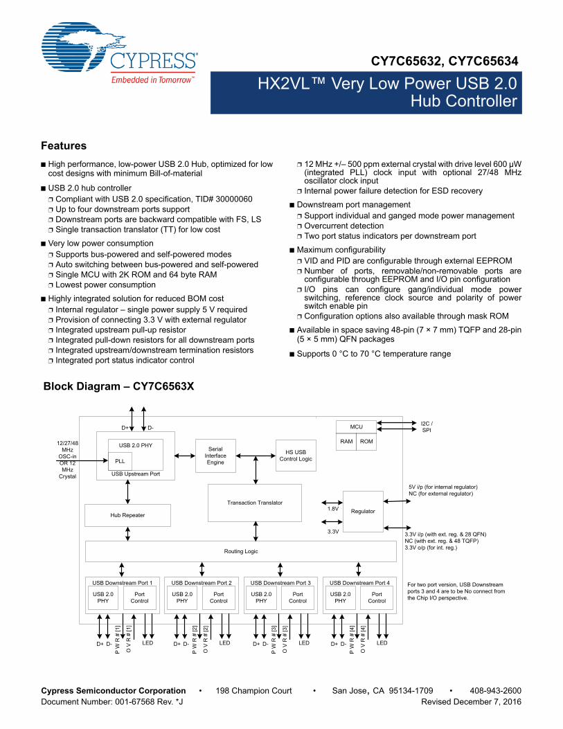
D+ D-
3.3V i/p (with ext. reg. & 28 QFN)NC (with ext. reg. & 48 TQFP)3.3V o/p (for int. reg.)
Hub Repeater
Routing Logic
USB Downstream Port 1
USB 2.0 PHY
Port Control
USB Downstream Port 2
USB 2.0 PHY
Port Control
USB Downstream Port 3
USB 2.0 PHY
Port Control
USB Downstream Port 4
USB 2.0 PHY
Port Control
MCU
RAM ROM
USB Upstream Port
USB 2.0 PHY
PLL
D+ D-
P W
R #
[1]
O V
R #
[1]
LED D+ D-
P W
R #
[2]
O V
R #
[2]
LED D+ D-
P W
R #
[3]
O V
R #
[3]
LED D+ D-
P W
R #
[4]
O V
R #
[4]
LED
I2C / SPI
12/27/48 MHz
OSC-in OR 12 MHz
Crystal
Transaction Translator
Regulator1.8V
Serial Interface Engine
HS USB Control Logic
3.3V
5V i/p (for internal regulator)NC (for external regulator)
For two port version, USB Downstream ports 3 and 4 are to be No connect from the Chip I/O perspective.
Block Diagram – CY7C6563X
CY7C65632, CY7C65634
Document Number: 001-67568 Rev. *J Page 2 of 29
More InformationCypress provides a wealth of data at www.cypress.com to help you to select the right HX2VL device for your design, and to help youto quickly and effectively integrate the device into your design. For a comprehensive list of resources, see the knowledge base articlehttp://www.cypress.com/?id=2411.
■ Overview: USB Portfolio, USB Roadmap
■ USB 2.0 Hub Controller Selectors: HX2LP, HX2VL
■ Application notes: Cypress offers a large number of USB appli-cation notes covering a broad range of topics, from basic to advanced level. Recommended application notes for getting started with HX2VL are:❐ AN72332 - Guidelines on System Design using Cypress's
USB 2.0 Hub (HX2VL)❐ AN69235 - Migrating from HX2/HX2LP to HX2VL
■ Reference Designs: ❐ CY4608 HX2VL Very Low-Power USB 2.0 Compliant 4-Port
Hub Development Kit❐ CY4607 HX2VL Very Low-Power USB 2.0 Compliant 4-Port
Hub Development Kit
■ Models: HX2VL (CY7C65632/34/42) - IBIS
HX2VL Development Kit
HX2VL Development Kit board is a tool to demonstrate the features of HX2VL devices (CY7C65632, CY7C65634). In the initial phase of the design, this board helps developers to understand the chip features and limitations before proceeding with a complete design. The Development kit includes support documents related to board hardware, PC application software, and EEPROM configuration data (.iic) files.
CY7C65632, CY7C65634
Document Number: 001-67568 Rev. *J Page 3 of 29
Contents
Introduction .......................................................................4HX2VL Architecture .......................................................... 4
USB Serial Interface Engine ........................................ 4HS USB Control Logic ................................................. 4Hub Repeater .............................................................. 4MCU ............................................................................ 4Transaction Translator ................................................ 4Port Control ................................................................. 4
Applications ...................................................................... 4Functional Overview ........................................................ 5
System Initialization ..................................................... 5Enumeration ................................................................ 5Upstream Port ............................................................. 5Downstream Ports ....................................................... 5Power Switching .......................................................... 5Overcurrent Detection ................................................. 5Port Indicators ............................................................. 5Power Regulator .......................................................... 6External Regulation Scheme ....................................... 6Internal Regulation Scheme ........................................ 6
Pin Configurations ........................................................... 7Pin Definitions ................................................................ 11Pin Definitions ................................................................ 14EEPROM Configuration Options ................................... 16Pin Configuration Options ............................................. 17
Power ON Reset .......................................................17Gang/Individual Power Switching Mode .................... 17Power Switch Enable Pin Polarity ............................. 17
Port Number Configuration ........................................ 17Non Removable Ports Configuration ......................... 17Reference Clock Configuration ................................. 18
Absolute Maximum Ratings .......................................... 19Operating Conditions ..................................................... 19Electrical Characteristics ............................................... 19
DC Electrical Characteristics ..................................... 19AC Electrical Characteristics ..................................... 21
Thermal Resistance ........................................................ 21Ordering Information ...................................................... 22
Ordering Code Definitions ......................................... 22Package Diagrams .......................................................... 23Acronyms ........................................................................ 25Document Conventions ................................................. 25
Units of Measure ....................................................... 25Silicon Errata for the HX2VL, CY7C65632 Product Family ........................................... 26
Part Numbers Affected .............................................. 26HX2VL Qualification Status ....................................... 26HX2VL Errata Summary ............................................ 26
Document History Page ................................................. 27Sales, Solutions, and Legal Information ...................... 29
Worldwide Sales and Design Support ....................... 29Products .................................................................... 29PSoC® Solutions ...................................................... 29Cypress Developer Community ................................. 29Technical Support ..................................................... 29
CY7C65632, CY7C65634
Document Number: 001-67568 Rev. *J Page 4 of 29
Introduction
HX2VL™ is Cypress’s next generation family of highperformance, very low power USB 2.0 hub controllers. HX2VLhas integrated upstream and downstream transceivers; a USBSerial Interface Engine (SIE); USB Hub Control and Repeaterlogic; and Transaction Translator (TT) logic. Cypress has alsointegrated external components such as voltage regulator andpull-up/pull-down resistors, reducing the overall bill of materialsrequired to implement a USB hub system.
The CY7C6563X is a part of the HX2VL portfolio. This deviceoption is for ultra low power but high performance applicationsthat require up to four downstream ports. All downstream portsshare a single transaction translator. The CY7C6563X isavailable in 48-pin TQFP and 28-pin QFN package options.
All device options are supported by Cypress’s world classreference design kits, which include board schematics, bill ofmaterials, Gerber files, Orcad files, and thorough designdocumentation.
HX2VL Architecture
The Block Diagram – CY7C6563X on page 1 shows the HX2VLsingle TT hub architecture.
USB Serial Interface Engine
The Serial Interface Engine (SIE) allows HX2VL to communicatewith the USB host. The SIE handles the following USB activitiesindependently of the Hub Control Block.
■ Bit stuffing and unstuffing
■ Checksum generation and checking
■ TOKEN type identification
■ Address checking
HS USB Control Logic
‘Hub Control’ block co-ordinates enumeration, suspend andresume. It generates status and control signals for host accessto the hub. It also includes the frame timer that synchronizes thehub to the host. It has status/control registers which function asthe interface to the firmware in the MCU.
Hub Repeater
The Hub Repeater manages the connectivity between upstreamand downstream facing ports that are operating at the samespeed. It supports full and high speed connectivity. According tothe USB 2.0 specification, the HUB Repeater provides thefollowing functions:
■ Sets up and tears down connectivity on packet boundaries
■ Ensures orderly entry into and out of ‘Suspend’ state, includingproper handling of remote wakeups.
MCU
HX2VL has MCU with 2K ROM and 64 byte RAM. The MCUoperates with a 12 MHz clock to decode USB commands fromhost and respond to the host. It can also handle GPIO settingsto provide higher flexibility to the customers and control the readinterface to the EEPROM which has extended configurationoptions. The MCU is programmable while manufacturing in thefactory as per customer needs.
Transaction Translator
The Transaction Translator translates data from one speed toanother. A TT takes high speed split transactions and translatesthem to full or low speed transactions when the hub is operatingat high speed (the upstream port is connected to a high speedhost controller) and has full or low speed devices attached. Theoperating speed of a device attached on a downstream portdetermines whether the routing logic connects a port to the TTor to hub repeater. When the upstream host and downstreamdevice are functioning at different speeds, the data is routedthrough the TT. In all other cases, the data is routed through therepeater. For example, If a full or low speed device is connectedto the high speed host upstream through the hub, then the datatransfer route includes TT. If a high speed device is connected tothe high speed host upstream through the hub, the transfer routeincludes the repeater. When the hub is connected to a full speedhost controller upstream, then high speed peripheral does notoperate at its full capability. These devices only work at fullspeed. Full and low speed devices connected to this hub operateat their normal speed.
Port Control
The downstream ‘Port Control’ block handles theconnect/disconnect and over current detection as well as thepower enable and LED control. It also generates the controlsignals for the downstream transceivers.
Applications
Typical applications for the HX2VL device family are:
■ Docking stations
■ Standalone hubs
■ Monitor hubs
■ Multi-function printers
■ Digital televisions
■ Advanced port replicators
■ Keyboard hubs
■ Gaming consoles
CY7C65632, CY7C65634
Document Number: 001-67568 Rev. *J Page 5 of 29
Functional Overview
The Cypress CY7C6563X USB 2.0 Hubs are low power hubsolutions for USB which provide maximum transfer efficiency.The CY7C6563X USB 2.0 Hubs integrate 1.5 kohm upstreampull-up resistors for full speed operation and all downstream15 kohm pull-down resistors and series termination resistors onall upstream and downstream D+ and D– pins. This results inoptimization of system costs by providing built-in support for theUSB 2.0 specification.
System Initialization
On power up, CY7C6563X has an option to enumerate from thedefault settings in the mask ROM or from reading an externalEEPROM for configuration information. At the most basic level,this EEPROM has the Vendor ID (VID) and the Product ID (PID),for the customer’s application. For more specializedapplications, other configuration options can be specified. SeeEEPROM Configuration Options on page 16 for more details.CY7C6563X verifies the checksum before loading the EEPROMcontents as the descriptors.
Enumeration
CY7C6563X enables the pull-up resistor on D+ to indicate itspresence to the upstream hub, after which a USB Bus Reset isexpected. After a USB Bus Reset, CY7C6563X is in anunaddressed, unconfigured state (configuration value set to ’0’).During the enumeration process, the host sets the hub's addressand configuration. After the hub is configured, the full hubfunctionality is available.
Upstream Port
The upstream port includes the transmitter and the receiver statemachine. The transmitter and receiver operate in high speed andfull speed depending on the current hub configuration. Thetransmitter state machine monitors the upstream facing portwhile the Hub Repeater has connectivity in the upstreamdirection. This machine prevents babble and disconnect eventson the downstream facing ports of this hub from propagating andcausing the hub to be disabled or disconnected by the hub towhich it is attached.
Downstream Ports
The CY7C6563X supports a maximum of four downstream ports,each of which may be marked as usable or removable in theEEPROM configuration, see EEPROM Configuration Options onpage 16. Additionallyit can also be configured by pin strapping,see Pin Configuration Options on page 17.
Downstream D+ and D– pull-down resistors are incorporated inCY7C6563X for each port. Before the hubs are configured, theports are driven SE0 (Single Ended Zero, where both D+ and D–are driven low) and are set to the unpowered state. When thehub is configured, the ports are not driven and the host maypower the ports by sending a SetPortPower command for eachport. After a port is powered, any connect or disconnect event isdetected by the hub. Any change in the port state is reported bythe hubs back to the host through the Status Change Endpoint(endpoint 1).
On receipt of SetPortReset request for a port with a deviceconnected, the hub does as follows:
■ Performs a USB Reset on the corresponding port
■ Puts the port in an enabled state
■ Enables babble detection after the port is enabled.
Babble consists of a non idle condition on the port after EOF2. Ifbabble is detected on an enabled port, that port is disabled. AClearPortEnable request from the host also disables thespecified port.
Downstream ports can be individually suspended by the hostwith the SetPortSuspend request. If the hub is not suspended, aremote wakeup event on that port is reflected to the host througha port change indication in the Hub Status Change Endpoint. Ifthe hub is suspended, a remote wakeup event on this port isforwarded to the host. The host may resume the port by sendinga ClearPortSuspend command.
Power Switching
The CY7C6563X includes interface signals for external portpower switches. Both ganged and individual (per-port)configurations are supported by pin strapping, see PinConfiguration Options on page 17.
After enumerating, the host may power each port by sending aSetPortPower request for that port. Power switching andovercurrent detection are managed using respective controlsignals (PWR#[n] and OVR#[n]) which are connected to anexternal power switch device. Both High/Low enabled powerswitches are supported and the polarity is configured throughGPIO setting, see Pin Configuration Options on page 17.
Overcurrent Detection
The OVR#[n] pins of the CY7C6563X series are connected tothe respective external power switch's port overcurrentindication (output) signals. After detecting an overcurrentcondition, hub reports overcurrent condition to the host anddisables the PWR#[n] output to the external power device.OVR#[n] has a setup time of 20 ns. It takes 3 to 4 ms fromovercurrent detection to de-assertion of PWR#[n]
Port Indicators
The USB 2.0 port indicators are also supported directly byCY7C6563X. According to the specification, each downstreamport of the hub optionally supports a status indicator. Thepresence of indicators for downstream facing ports is specifiedby bit 7 of the wHub Characteristics field of the hub classdescriptor. The default CY7C6563X descriptor specifies that theport indicators are supported. The CY7C6563X port indicatorshas two modes of operation: automatic and manual.
On power up the CY7C6563X defaults to automatic mode, wherethe color of the Port Indicator (green, amber, off) indicates thefunctional status of the CY7C6563X port. The LEDs are turnedoff when the device is suspended.
CY7C65632, CY7C65634
Document Number: 001-67568 Rev. *J Page 6 of 29
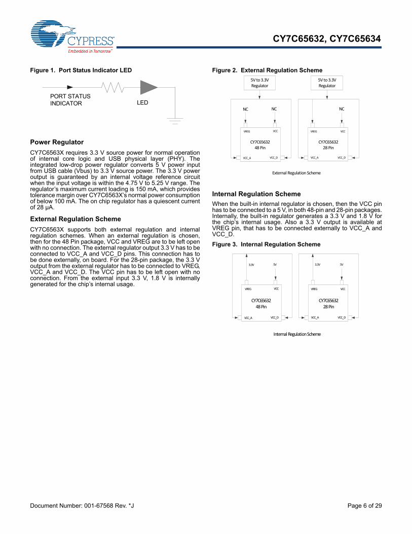
Figure 1. Port Status Indicator LED
Power Regulator
CY7C6563X requires 3.3 V source power for normal operationof internal core logic and USB physical layer (PHY). Theintegrated low-drop power regulator converts 5 V power inputfrom USB cable (Vbus) to 3.3 V source power. The 3.3 V poweroutput is guaranteed by an internal voltage reference circuitwhen the input voltage is within the 4.75 V to 5.25 V range. Theregulator’s maximum current loading is 150 mA, which providestolerance margin over CY7C6563X’s normal power consumptionof below 100 mA. The on chip regulator has a quiescent currentof 28 µA.
External Regulation Scheme
CY7C6563X supports both external regulation and internalregulation schemes. When an external regulation is chosen,then for the 48 Pin package, VCC and VREG are to be left openwith no connection. The external regulator output 3.3 V has to beconnected to VCC_A and VCC_D pins. This connection has tobe done externally, on board. For the 28-pin package, the 3.3 Voutput from the external regulator has to be connected to VREG,VCC_A and VCC_D. The VCC pin has to be left open with noconnection. From the external input 3.3 V, 1.8 V is internallygenerated for the chip’s internal usage.
Figure 2. External Regulation Scheme
Internal Regulation Scheme
When the built-in internal regulator is chosen, then the VCC pinhas to be connected to a 5 V, in both 48-pin and 28-pin packages.Internally, the built-in regulator generates a 3.3 V and 1.8 V forthe chip’s internal usage. Also a 3.3 V output is available atVREG pin, that has to be connected externally to VCC_A andVCC_D.
Figure 3. Internal Regulation Scheme
PORT STATUS INDICATOR LED
VCC_D
VCC
External Regulation Scheme
VCC_A
VREG
NC NC
5V to 3.3VRegulator
VCC_A VCC_D
VREG VCC
NC
5V to 3.3VRegulator
CY7C6563248 Pin
CY7C6563228 Pin
3.3V 3.3V
VCC_D
VCC
Internal Regulation Scheme
VCC_A
VREG
5V
VCC_A VCC_D
VREG VCC
5V
CY7C6563248 Pin
CY7C6563228 Pin
CY7C65632, CY7C65634
Document Number: 001-67568 Rev. *J Page 7 of 29
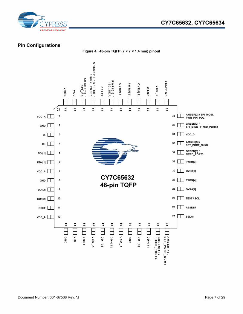
Pin ConfigurationsFigure 4. 48-pin TQFP (7 × 7 × 1.4 mm) pinout
AMBER[2] / SPI_MOSI /PWR_PIN_POL
36
GREEN[2] /SPI_MISO / FIXED_PORT2
35
VCC_D34
AMBER[3] / SET_PORT_NUM2
33
GREEN[3] / FIXED_PORT3
32
PWR#[3]31
OVR#[3]30
PWR#[4]29
OVR#[4]28
TEST / SCL27
RESET#26
SEL4825
VCC_A 1
GND 2
D- 3
D+ 4
DD-[1] 5
DD+[1] 6
VCC_A 7
GND 8
DD-[2] 9
DD+[2] 10
RREF 11
VCC_A 12
AM
BE
R[4
] / S
ET
_P
OR
T_
NU
M1
24
GR
EE
N[4
] / F
IXE
D_
PO
RT
42
3
DD
+[4
]2
2
DD
-[4]
21
GN
D2
0
VC
C_
A1
9
DD
+[3
]1
8
DD
-[3]
17
VC
C_
A1
6
XO
UT
15
XIN
14
GN
D1
3
SE
LF
PW
R3
7
VC
C_
D3
8
GA
NG
39
OV
R#
[2]
40
PW
R#
[2]
41
OV
R#
[1]
42
PW
R#
[1] /
I2C
_S
DA
43
SE
L2
74
4
GR
EE
N[1
] / SP
I_S
K /
FIX
ED
_P
OR
T1
45
AM
BE
R[1
] / S
PI_
CS
46
VC
C4
7
VR
EG
48
CY7C65632 48-pin TQFP
CY7C65632, CY7C65634
Document Number: 001-67568 Rev. *J Page 8 of 29
Figure 5. 48-pin TQFP (7 × 7 × 1.4 mm) pinout
Pin Configurations (continued)
AMBER[2] / SPI_MOSI /PWR_PIN_POL
36
GREEN[2] /SPI_MISO/ FIXED_PORT2
35
VCC_D34
NC33
NC32
NC31
NC30
NC29
NC28
TEST / SCL27
RESET#26
SEL4825
VCC_A 1
GND 2
D- 3
D+ 4
DD-[1] 5
DD+[1] 6
VCC_A 7
GND 8
DD-[2] 9
DD+[2] 10
RREF 11
VCC_A 12
NC
24
NC
23
NC
22
NC
21
GN
D2
0
NC
19
NC
18
NC
17
VC
C_
A1
6
XO
UT
15
XIN
14
GN
D1
3
SE
LF
PW
R3
7
VC
C_
D3
8
GA
NG
39
OV
R#
[2]
40
PW
R#
[2]
41
OV
R#
[1]
42
PW
R#
[1] /
I2C
_S
DA
43
SE
L2
74
4
GR
EE
N[1
] / SP
I_S
K /
FIX
ED
_P
OR
T1
45
AM
BE
R[1
] / S
PI_
CS
46
VC
C4
7
VR
EG
48
Two Port
CY7C65634 48-pin TQFP
CY7C65632, CY7C65634
Document Number: 001-67568 Rev. *J Page 9 of 29
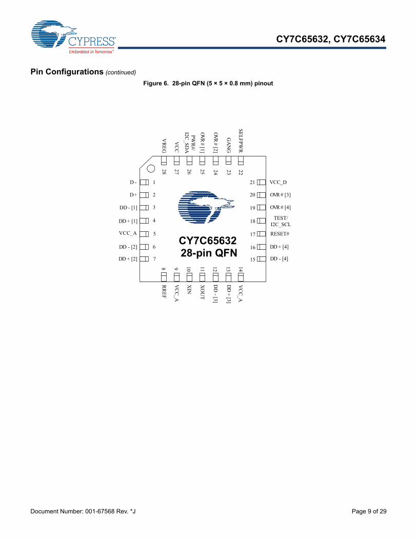
Figure 6. 28-pin QFN (5 × 5 × 0.8 mm) pinout
Pin Configurations (continued)
D+
DD - [1]
VCC A_
OVR # [3]
1
2
3
4
5
6
18
17
16
15
12111098
222324
-X
IN
RR
EF
SE
LF
PW
R
GA
NG
VC
C
VR
EG
TEST/I2C_SCL
RESET#
7
141321
20
1925262728
XO
UT
PW
R#/
I2C_SD
A
D -
DD + [1]
DD + [4]
DD - [4]DD + [2]
DD - [2]
DD
+ [3]
DD
- [3]
VC
CA_
VC
CA_
VCC D_
OVR # [4]O
VR
# [1]
OV
R# [2]
28-pin QFNCY7C65632
CY7C65632, CY7C65634
Document Number: 001-67568 Rev. *J Page 10 of 29
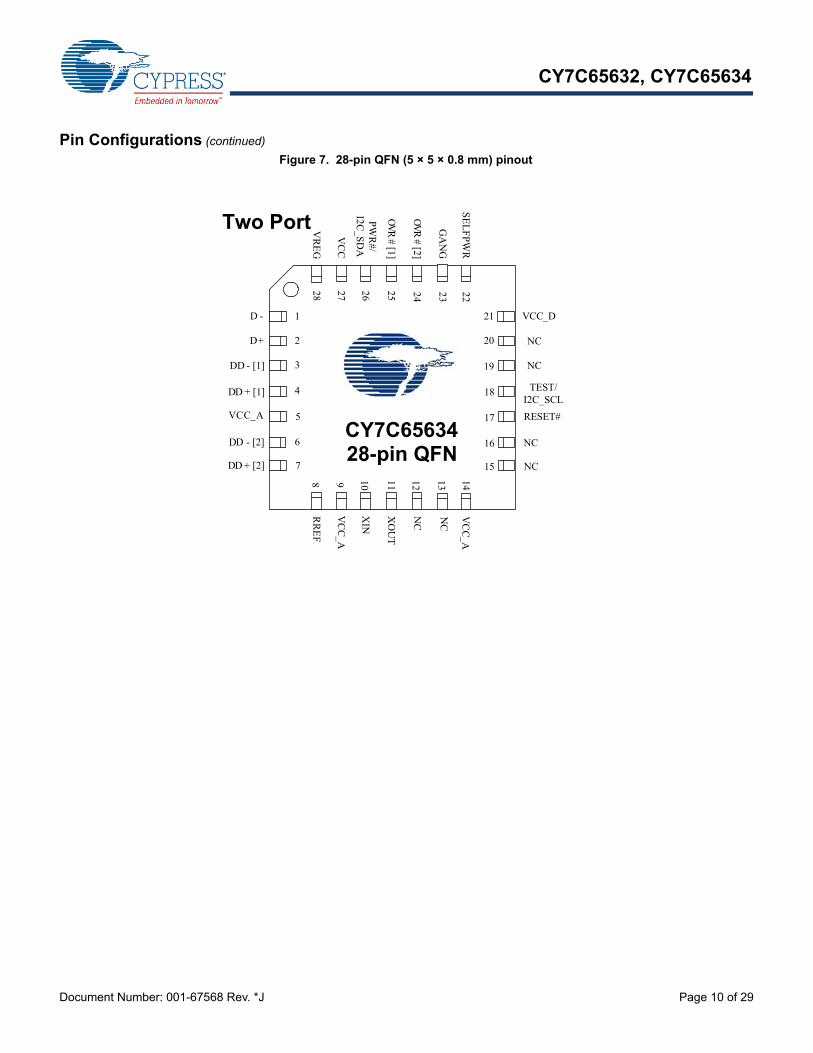
Figure 7. 28-pin QFN (5 × 5 × 0.8 mm) pinout
Pin Configurations (continued)
D+
DD - [1]
VCC A_
1
2
3
4
5
6
18
17
16
15
12111098
222324
-X
IN
RR
EF
SE
LF
PW
R
GA
NG
VC
C
VR
EG
TEST/I2C_SCL
RESET#
7
1413
21
20
19
25262728
XO
UT
PW
R#/
I2C_SD
A
D -
DD + [1]
DD + [2]
DD - [2]
VC
CA_
VC
CA_
VCC D_
OV
R# [1]
OV
R# [2]
28-pin QFNCY7C65634
Two Port
NC
NC
NC
NC
NC
NC
CY7C65632, CY7C65634
Document Number: 001-67568 Rev. *J Page 11 of 29
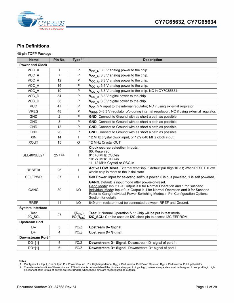
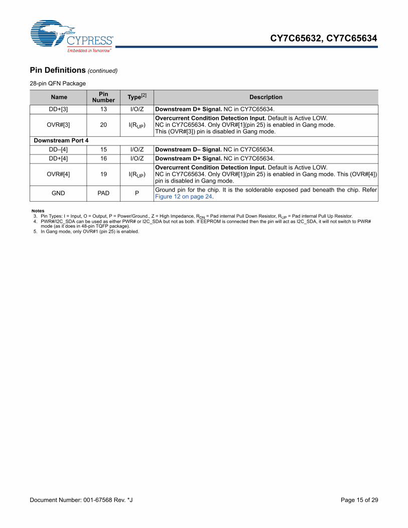
Pin Definitions
48-pin TQFP Package
Name Pin No. Type [1] Description
Power and Clock
VCC_A 1 P VCC_A. 3.3 V analog power to the chip.
VCC_A 7 P VCC_A. 3.3 V analog power to the chip.
VCC_A 12 P VCC_A. 3.3 V analog power to the chip.
VCC_A 16 P VCC_A. 3.3 V analog power to the chip.
VCC_A 19 P VCC_A. 3.3 V analog power to the chip. NC in CY7C65634.
VCC_D 34 P VCC_D. 3.3 V digital power to the chip.
VCC_D 38 P VCC_D. 3.3 V digital power to the chip.
VCC 47 P VCC. 5 V input to the internal regulator; NC if using external regulator
VREG 48 P VREG. 5–3.3 V regulator o/p during internal regulation; NC if using external regulator.
GND 2 P GND. Connect to Ground with as short a path as possible.
GND 8 P GND. Connect to Ground with as short a path as possible.
GND 13 P GND. Connect to Ground with as short a path as possible.
GND 20 P GND. Connect to Ground with as short a path as possible.
XIN 14 I 12 MHz crystal clock input, or 12/27/48 MHz clock input.
XOUT 15 O 12 MHz Crystal OUT
SEL48/SEL27 25 / 44 I
Clock source selection inputs.00: Reserved01: 48 MHz OSC-in10: 27 MHz OSC-in11: 12 MHz Crystal or OSC-in
RESET# 26 IActive LOW Reset. External reset input, default pull high 10 k; When RESET = low, whole chip is reset to the initial state.
SELFPWR 37 I Self Power. Input for selecting self/bus power. 0 is bus powered, 1 is self powered.
GANG 39 I/O
GANG. Default is input mode after power-on-reset.Gang Mode: Input:1 -> Output is 0 for Normal Operation and 1 for SuspendIndividual Mode: Input:0 -> Output is 1 for Normal Operation and 0 for SuspendRefer to Gang/Individual Power Switching Modes in Pin Configuration Options Section for details
RREF 11 I/O 649 ohm resistor must be connected between RREF and Ground.
System Interface
TestI2C_SCL 27 I(RDN)
I/O(RDN)Test: 0: Normal Operation & 1: Chip will be put in test mode.I2C_SCL: Can be used as I2C clock pin to access I2C EEPROM.
Upstream Port
D– 3 I/O/Z Upstream D– Signal.
D+ 4 I/O/Z Upstream D+ Signal.
Downstream Port 1
DD–[1] 5 I/O/Z Downstream D– Signal. Downstream D- signal of port 1.
DD+[1] 6 I/O/Z Downstream D+ Signal. Downstream D+ signal of port 1.
Notes1. Pin Types: I = Input, O = Output, P = Power/Ground., Z = High Impedance, RDN = Pad internal Pull Down Resistor, RUP = Pad internal Pull Up Resistor.2. The alternate function of these pins as LED indicator is not available if the pins are strapped to logic high, unless a separate circuit is designed to support logic high
disconnect after 60 ms of power-on reset (POR), when these pins are reconfigured as outputs.
CY7C65632, CY7C65634
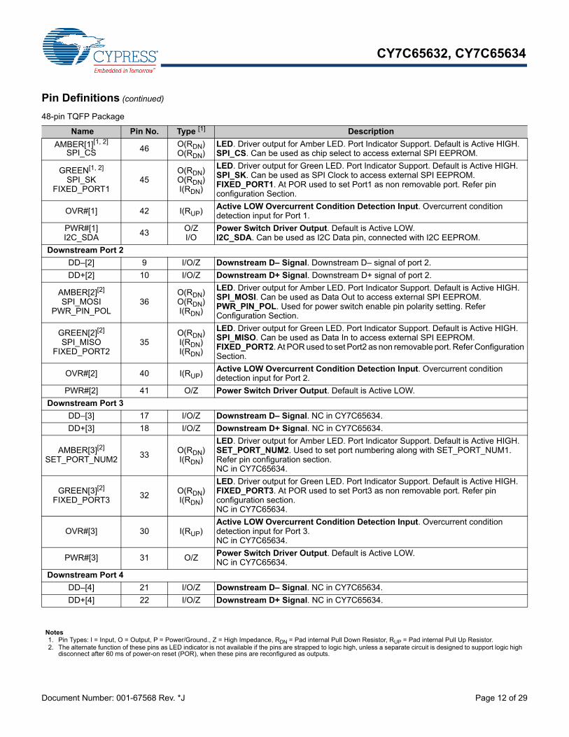
Document Number: 001-67568 Rev. *J Page 12 of 29
AMBER[1][1, 2]
SPI_CS 46 O(RDN)O(RDN)
LED. Driver output for Amber LED. Port Indicator Support. Default is Active HIGH.SPI_CS. Can be used as chip select to access external SPI EEPROM.
GREEN[1, 2]
SPI_SKFIXED_PORT1
45O(RDN)O(RDN)I(RDN)
LED. Driver output for Green LED. Port Indicator Support. Default is Active HIGH.SPI_SK. Can be used as SPI Clock to access external SPI EEPROM.FIXED_PORT1. At POR used to set Port1 as non removable port. Refer pin configuration Section.
OVR#[1] 42 I(RUP)Active LOW Overcurrent Condition Detection Input. Overcurrent condition detection input for Port 1.
PWR#[1]I2C_SDA
43 O/ZI/O
Power Switch Driver Output. Default is Active LOW. I2C_SDA. Can be used as I2C Data pin, connected with I2C EEPROM.
Downstream Port 2
DD–[2] 9 I/O/Z Downstream D– Signal. Downstream D– signal of port 2.
DD+[2] 10 I/O/Z Downstream D+ Signal. Downstream D+ signal of port 2.
AMBER[2][2]
SPI_MOSIPWR_PIN_POL
36O(RDN)O(RDN)I(RDN)
LED. Driver output for Amber LED. Port Indicator Support. Default is Active HIGH. SPI_MOSI. Can be used as Data Out to access external SPI EEPROM. PWR_PIN_POL. Used for power switch enable pin polarity setting. Refer Configuration Section.
GREEN[2][2]
SPI_MISOFIXED_PORT2
35O(RDN)I(RDN)I(RDN)
LED. Driver output for Green LED. Port Indicator Support. Default is Active HIGH. SPI_MISO. Can be used as Data In to access external SPI EEPROM.FIXED_PORT2. At POR used to set Port2 as non removable port. Refer Configuration Section.
OVR#[2] 40 I(RUP) Active LOW Overcurrent Condition Detection Input. Overcurrent condition detection input for Port 2.
PWR#[2] 41 O/Z Power Switch Driver Output. Default is Active LOW.
Downstream Port 3
DD–[3] 17 I/O/Z Downstream D– Signal. NC in CY7C65634.
DD+[3] 18 I/O/Z Downstream D+ Signal. NC in CY7C65634.
AMBER[3][2]
SET_PORT_NUM233 O(RDN)
I(RDN)
LED. Driver output for Amber LED. Port Indicator Support. Default is Active HIGH. SET_PORT_NUM2. Used to set port numbering along with SET_PORT_NUM1. Refer pin configuration section.NC in CY7C65634.
GREEN[3][2]
FIXED_PORT332 O(RDN)
I(RDN)
LED. Driver output for Green LED. Port Indicator Support. Default is Active HIGH. FIXED_PORT3. At POR used to set Port3 as non removable port. Refer pin configuration section.NC in CY7C65634.
OVR#[3] 30 I(RUP)Active LOW Overcurrent Condition Detection Input. Overcurrent condition detection input for Port 3.NC in CY7C65634.
PWR#[3] 31 O/Z Power Switch Driver Output. Default is Active LOW. NC in CY7C65634.
Downstream Port 4
DD–[4] 21 I/O/Z Downstream D– Signal. NC in CY7C65634.
DD+[4] 22 I/O/Z Downstream D+ Signal. NC in CY7C65634.
Pin Definitions (continued)
48-pin TQFP Package
Name Pin No. Type [1] Description
Notes1. Pin Types: I = Input, O = Output, P = Power/Ground., Z = High Impedance, RDN = Pad internal Pull Down Resistor, RUP = Pad internal Pull Up Resistor.2. The alternate function of these pins as LED indicator is not available if the pins are strapped to logic high, unless a separate circuit is designed to support logic high
disconnect after 60 ms of power-on reset (POR), when these pins are reconfigured as outputs.
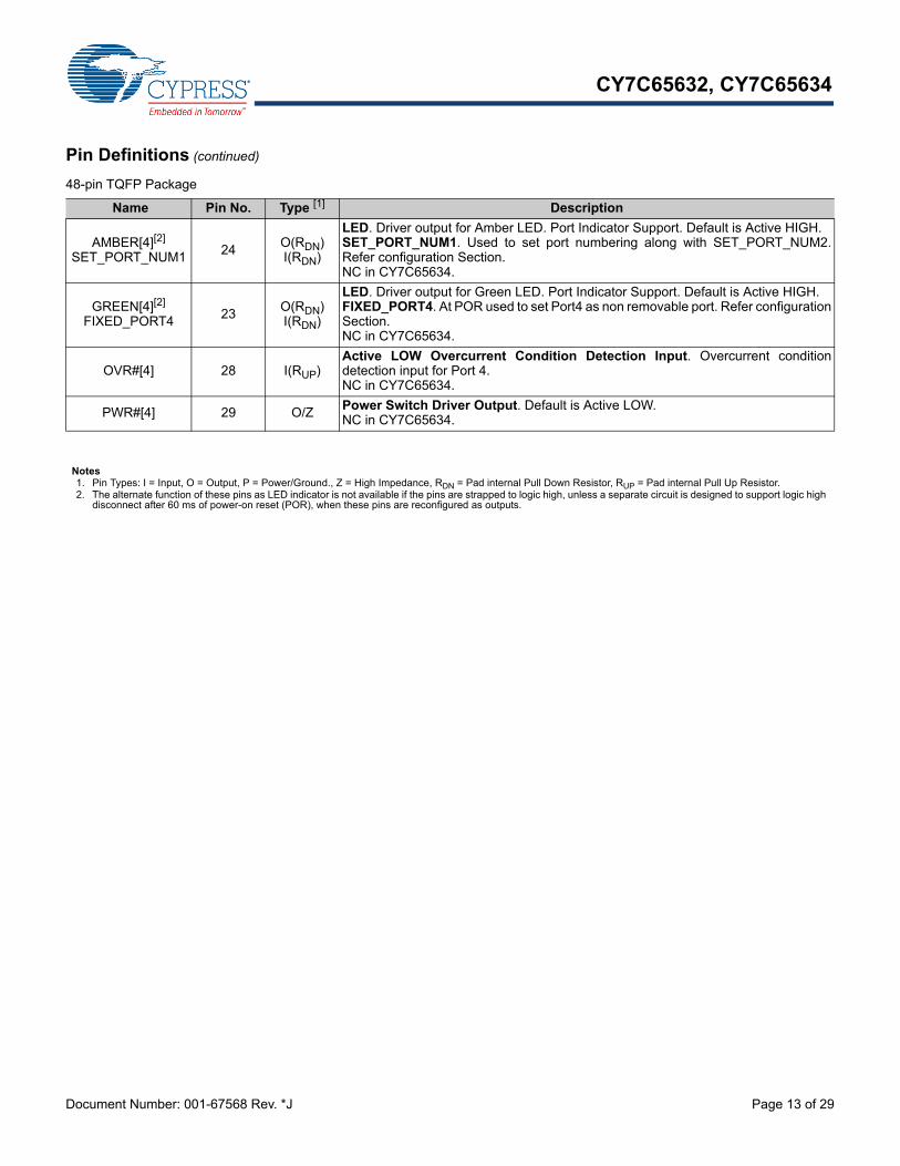
CY7C65632, CY7C65634
Document Number: 001-67568 Rev. *J Page 13 of 29
AMBER[4][2]
SET_PORT_NUM1 24O(RDN)I(RDN)
LED. Driver output for Amber LED. Port Indicator Support. Default is Active HIGH. SET_PORT_NUM1. Used to set port numbering along with SET_PORT_NUM2.Refer configuration Section.NC in CY7C65634.
GREEN[4][2]
FIXED_PORT4 23O(RDN)I(RDN)
LED. Driver output for Green LED. Port Indicator Support. Default is Active HIGH. FIXED_PORT4. At POR used to set Port4 as non removable port. Refer configurationSection.NC in CY7C65634.
OVR#[4] 28 I(RUP)Active LOW Overcurrent Condition Detection Input. Overcurrent conditiondetection input for Port 4.NC in CY7C65634.
PWR#[4] 29 O/Z Power Switch Driver Output. Default is Active LOW. NC in CY7C65634.
Pin Definitions (continued)
48-pin TQFP Package
Name Pin No. Type [1] Description
Notes1. Pin Types: I = Input, O = Output, P = Power/Ground., Z = High Impedance, RDN = Pad internal Pull Down Resistor, RUP = Pad internal Pull Up Resistor.2. The alternate function of these pins as LED indicator is not available if the pins are strapped to logic high, unless a separate circuit is designed to support logic high
disconnect after 60 ms of power-on reset (POR), when these pins are reconfigured as outputs.
CY7C65632, CY7C65634
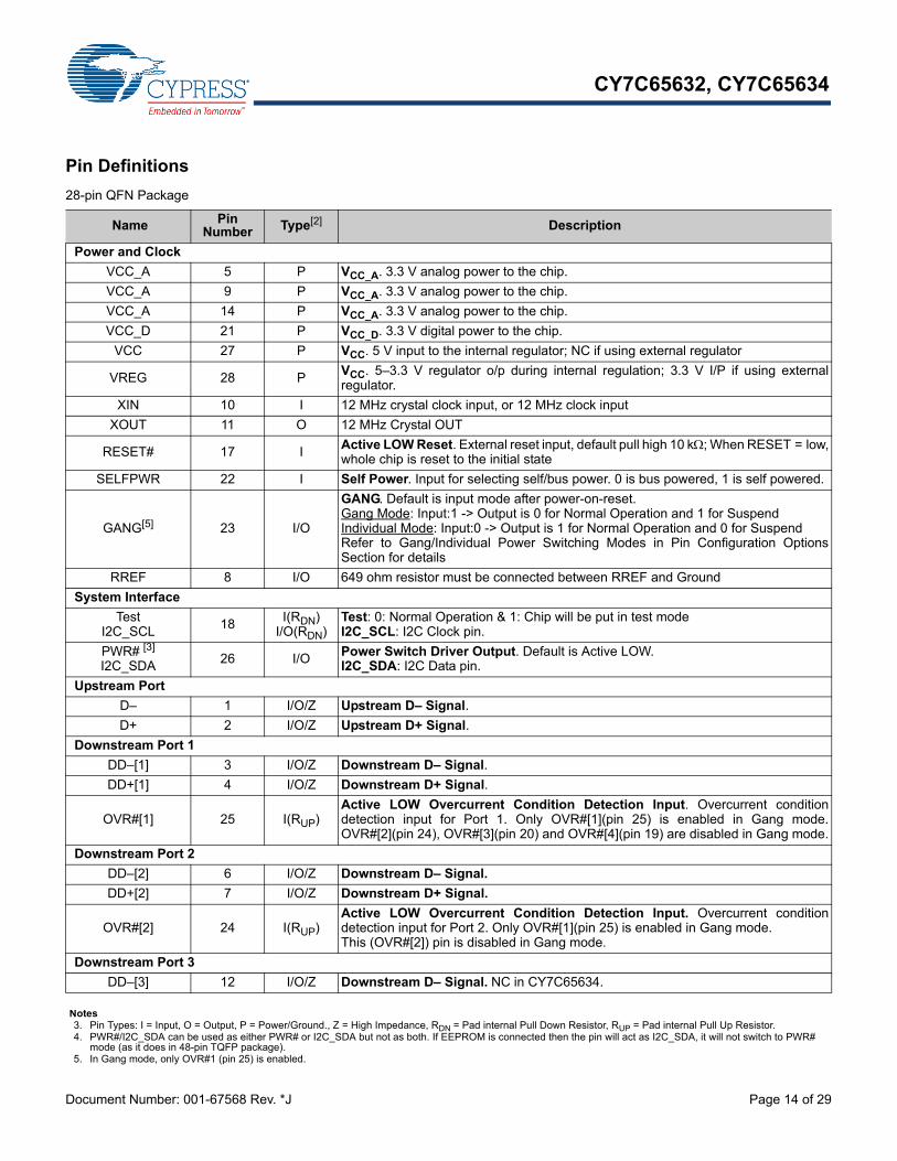
Document Number: 001-67568 Rev. *J Page 14 of 29
Pin Definitions
28-pin QFN Package
Name Pin Number Type[2] Description
Power and Clock
VCC_A 5 P VCC_A. 3.3 V analog power to the chip.
VCC_A 9 P VCC_A. 3.3 V analog power to the chip.
VCC_A 14 P VCC_A. 3.3 V analog power to the chip.
VCC_D 21 P VCC_D. 3.3 V digital power to the chip.
VCC 27 P VCC. 5 V input to the internal regulator; NC if using external regulator
VREG 28 P VCC. 5–3.3 V regulator o/p during internal regulation; 3.3 V I/P if using externalregulator.
XIN 10 I 12 MHz crystal clock input, or 12 MHz clock input
XOUT 11 O 12 MHz Crystal OUT
RESET# 17 I Active LOW Reset. External reset input, default pull high 10 k; When RESET = low,whole chip is reset to the initial state
SELFPWR 22 I Self Power. Input for selecting self/bus power. 0 is bus powered, 1 is self powered.
GANG[5] 23 I/O
GANG. Default is input mode after power-on-reset.Gang Mode: Input:1 -> Output is 0 for Normal Operation and 1 for SuspendIndividual Mode: Input:0 -> Output is 1 for Normal Operation and 0 for SuspendRefer to Gang/Individual Power Switching Modes in Pin Configuration OptionsSection for details
RREF 8 I/O 649 ohm resistor must be connected between RREF and Ground
System Interface
TestI2C_SCL
18 I(RDN)I/O(RDN)
Test: 0: Normal Operation & 1: Chip will be put in test modeI2C_SCL: I2C Clock pin.
PWR# [3]
I2C_SDA 26 I/O Power Switch Driver Output. Default is Active LOW.I2C_SDA: I2C Data pin.
Upstream Port
D– 1 I/O/Z Upstream D– Signal.
D+ 2 I/O/Z Upstream D+ Signal.
Downstream Port 1
DD–[1] 3 I/O/Z Downstream D– Signal.
DD+[1] 4 I/O/Z Downstream D+ Signal.
OVR#[1] 25 I(RUP)Active LOW Overcurrent Condition Detection Input. Overcurrent conditiondetection input for Port 1. Only OVR#[1](pin 25) is enabled in Gang mode.OVR#[2](pin 24), OVR#[3](pin 20) and OVR#[4](pin 19) are disabled in Gang mode.
Downstream Port 2
DD–[2] 6 I/O/Z Downstream D– Signal.
DD+[2] 7 I/O/Z Downstream D+ Signal.
OVR#[2] 24 I(RUP)Active LOW Overcurrent Condition Detection Input. Overcurrent conditiondetection input for Port 2. Only OVR#[1](pin 25) is enabled in Gang mode. This (OVR#[2]) pin is disabled in Gang mode.
Downstream Port 3
DD–[3] 12 I/O/Z Downstream D– Signal. NC in CY7C65634.
Notes3. Pin Types: I = Input, O = Output, P = Power/Ground., Z = High Impedance, RDN = Pad internal Pull Down Resistor, RUP = Pad internal Pull Up Resistor.4. PWR#/I2C_SDA can be used as either PWR# or I2C_SDA but not as both. If EEPROM is connected then the pin will act as I2C_SDA, it will not switch to PWR#
mode (as it does in 48-pin TQFP package).5. In Gang mode, only OVR#1 (pin 25) is enabled.
CY7C65632, CY7C65634
Document Number: 001-67568 Rev. *J Page 15 of 29
DD+[3] 13 I/O/Z Downstream D+ Signal. NC in CY7C65634.
OVR#[3] 20 I(RUP)Overcurrent Condition Detection Input. Default is Active LOW. NC in CY7C65634. Only OVR#[1](pin 25) is enabled in Gang mode.This (OVR#[3]) pin is disabled in Gang mode.
Downstream Port 4
DD–[4] 15 I/O/Z Downstream D– Signal. NC in CY7C65634.
DD+[4] 16 I/O/Z Downstream D+ Signal. NC in CY7C65634.
OVR#[4] 19 I(RUP)Overcurrent Condition Detection Input. Default is Active LOW. NC in CY7C65634. Only OVR#[1](pin 25) is enabled in Gang mode. This (OVR#[4])pin is disabled in Gang mode.
GND PAD PGround pin for the chip. It is the solderable exposed pad beneath the chip. ReferFigure 12 on page 24.
Pin Definitions (continued)
28-pin QFN Package
Name Pin Number Type[2] Description
Notes3. Pin Types: I = Input, O = Output, P = Power/Ground., Z = High Impedance, RDN = Pad internal Pull Down Resistor, RUP = Pad internal Pull Up Resistor.4. PWR#/I2C_SDA can be used as either PWR# or I2C_SDA but not as both. If EEPROM is connected then the pin will act as I2C_SDA, it will not switch to PWR#
mode (as it does in 48-pin TQFP package).5. In Gang mode, only OVR#1 (pin 25) is enabled.
CY7C65632, CY7C65634
Document Number: 001-67568 Rev. *J Page 16 of 29
EEPROM Configuration Options
Systems using CY7C6563X have the option of using the defaultdescriptors to configure the hub. Otherwise, it must have anexternal EEPROM for the device to have a unique VID, and PID.The CY7C6563X can communicate with an SPI (microwire)EEPROM like 93C46 or I2C EEPROM like 24C02. ExampleEEPROM connections are as shown in the following figure.
Figure 8. EEPROM Connections
Note The 28-pin QFN package includes only support for I2CEEPROM like ATMEL/24C02N_SU27 D, MICROCHIP/4LC028SN0509, SEIKO/S24CS02AVH9. The 48-pin TQFP packageincludes both I2C and SPI EEPROM connectivity options. In thiscase, user can use either SPI or I2C connectivity at a time forcommunicating to EEPROM. The 48-pin package supportsATMEL/AT93C46DN-SH-T, in addition to the above mentionedfamilies. HX2VL can only read from SPI EEPROM. So, fieldprogramming of EEPROM is supported only for I2C EEPROM.
CY7C6563X verifies the check sum after power on reset and ifvalidated loads the configuration from the EEPROM. To preventthis configuration from being overwritten, AMBER[1] is disabledwhen SPI EEPROM is present.
Default VID is 0x4B4, PID is 0x6570.
Byte 0: VID (LSB)
Least Significant Byte of Vendor ID
Byte 1: VID (MSB)
Most Significant Byte of Vendor ID
Byte2: PID (LSB)
Least Significant Byte of Product ID
Byte 3: PID (MSB)
Most Significant Byte of Product ID
Byte 4: ChkSum
CY7C6563X will ignore the EEPROM settings if ChkSum isnot equal to VID_LSB + VID_MSB + PID_LSB + PID_MSB +1
Byte 5: Reserved
Set to FEh
Byte 6: RemovablePorts
RemovablePorts[4:1] are the bits that indicates whether thedevice attached to the corresponding downstream port isremovable (set to 0) or non-removable (set to 1). Bit 1corresponds to Port 1, Bit 2 to Port 2 and so on. Default valueis 0 (removable). These bit values are reported appropriatelyin the HubDescriptor:DeviceRemovable field.
Bits 0,5,6,7 are set to 0.
Byte 7: Port Number
Port Number indicates the number of downstream ports. Thevalues must be 1 to 4. Default value is 4.
Byte 8: Maximum Power
This value is reported in the Configuration Descriptor:bMax-Power field and is the current in 2 mA increments thatis required from the upstream hubs. The allowed range is 00h(0 mA) to FAh(500 mA). Default value is 32h (100mA).
Byte 9–15: Reserved
Set to FFh
Byte 16: Vendor String Length
Length of the Vendor String
Byte 17–63: Vendor String
Value of Vendor String.
Table 1. EEPROM Configuration Options
Byte Value
00h VID_LSB
01h VID_MSB
02h PID_LSB
03h PID_MSB
04h ChkSum
05h Reserved - FEh
06h Removable Ports
07h Port Number
08h Maximum Power
CS
DI
SK
DO GND
NC2
NC1
VCCAMBER#[1]
AMBER#[2]
GREEN#[1]
GREEN#[2]
VDD
AT93C46
A0
A2
A1
GND SDA
SCL
WP
VCC
TEST
AT24C02
VDD
PWR#[1]
I2C EEPROM Connection
SPI EEPROM Connection
09h–0Fh Reserved - FFh
10h Vendor String Length
11h–3Fh Vendor String (ASCII code)
40h Product String Length
41h–6Fh Product String (ASCII Code)
70h Serial Number Length
71h to 80h onwards Serial Number String
Table 1. EEPROM Configuration Options (continued)
Byte Value
CY7C65632, CY7C65634
Document Number: 001-67568 Rev. *J Page 17 of 29
Byte 64: Product String Length
Length of the Product String
Byte 65–111: Product String
Value of Product String.
Byte 112: Serial Number Length
Length of the Serial Number
Byte 113 onwards: Serial Number String
Serial Number String.
Pin Configuration Options
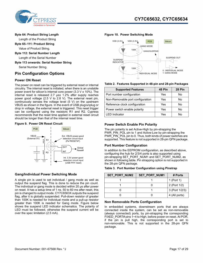
Power ON Reset
The power on reset can be triggered by external reset or internalcircuitry. The internal reset is initiated, when there is an unstablepower event for silicon’s internal core power (3.3 V ± 10%). Theinternal reset is released 2.7 µs± 1.2% after supply reachespower good voltage (2.5 V to 2.8 V). The external reset pin,continuously senses the voltage level (5 V) on the upstreamVBUS as shown in the figure. In the event of USB plug/unplug ordrop in voltage, the external reset is triggered. This reset triggercan be configured using the resistors R1 and R2. Cypressrecommends that the reset time applied in external reset circuitshould be longer than that of the internal reset time.
Figure 9. Power ON Reset Circuit
Gang/Individual Power Switching Mode
A single pin is used to set individual / gang mode as well asoutput the suspend flag. This is done to reduce the pin count.The individual or gang mode is decided within 20 µs after poweron reset. It has a setup time of 1 ns. 50 to 60 ms after reset, thispin is changed to output mode. CY7C6563X outputs the suspendflag, after it is globally suspended. Pull-down resistor of greaterthan 100K is needed for Individual mode and a pull-up resistorgreater than 100K is needed for Gang mode. Figure belowshows the suspend LED indicator schematics. The polarity ofLED must be followed, otherwise the suspend current will beover the spec limitation (2.5 mA).
Figure 10. Power Switching Mode
Power Switch Enable Pin Polarity
The pin polarity is set Active-High by pin-strapping the PWR_PIN_POL pin to 1 and Active-Low by pin-strapping the PWR_PIN_POL pin to 0. Thus, both kinds of power switches are supported. This feature is not supported in 28-pin QFN package.
Port Number Configuration
In addition to the EEPROM configuration, as described above, configuring the hub for 2/3/4 ports is also supported using pin-strapping SET_PORT_NUM1 and SET_PORT_NUM2, as shown in following table. Pin strapping option is not supported in the 28-pin QFN package.
Table 3. Port Number Configuration using Pinstrap
Non Removable Ports Configuration
In embedded systems, downstream ports that are alwaysconnected inside the system, can be set as non-removable(always connected) ports, by pin-strapping the correspondingFIXED_PORT# pins 1~4 to High, before power on reset. At POR,if the pin is pull high, the corresponding port is set tonon-removable. This is not supported in the 28-pin QFNpackage.
Global Reset#
Int. 3.3V power-good detection circuit input
(USB PHY reset)
Ext. VBUS power-good detection circuit input
(Pin"RESET#")
VBUS(External 5V)
R1
R2 INT
EXT
PCB Silicon
Table 2. Features Supported in 48-pin and 28-pin Packages
Supported Features 48 Pin 28 Pin
Port number configuration Yes No
Non-Removable port configuration Yes No
Reference clock configuration Yes No
Power switch enable polarity Yes No
LED Indicator Yes No
SET_PORT_NUM2 SET_PORT_NUM1 # Ports
1 1 1 (Port 1)
1 0 2 (Port 1/2)
0 1 3 (Port 1/2/3)
0 0 4 (All ports)
0 : INDIVIDUAL MODE1: GANG MODE
SUSPEND OUT
VDD (3.3V)
SUSPEND INDICATOR
VDD (3.3V)
100K
100K
GANG/SUSPEND
SiliconPCB
GANG MODE
INDIVIDUAL MODE
CY7C65632, CY7C65634
Document Number: 001-67568 Rev. *J Page 18 of 29
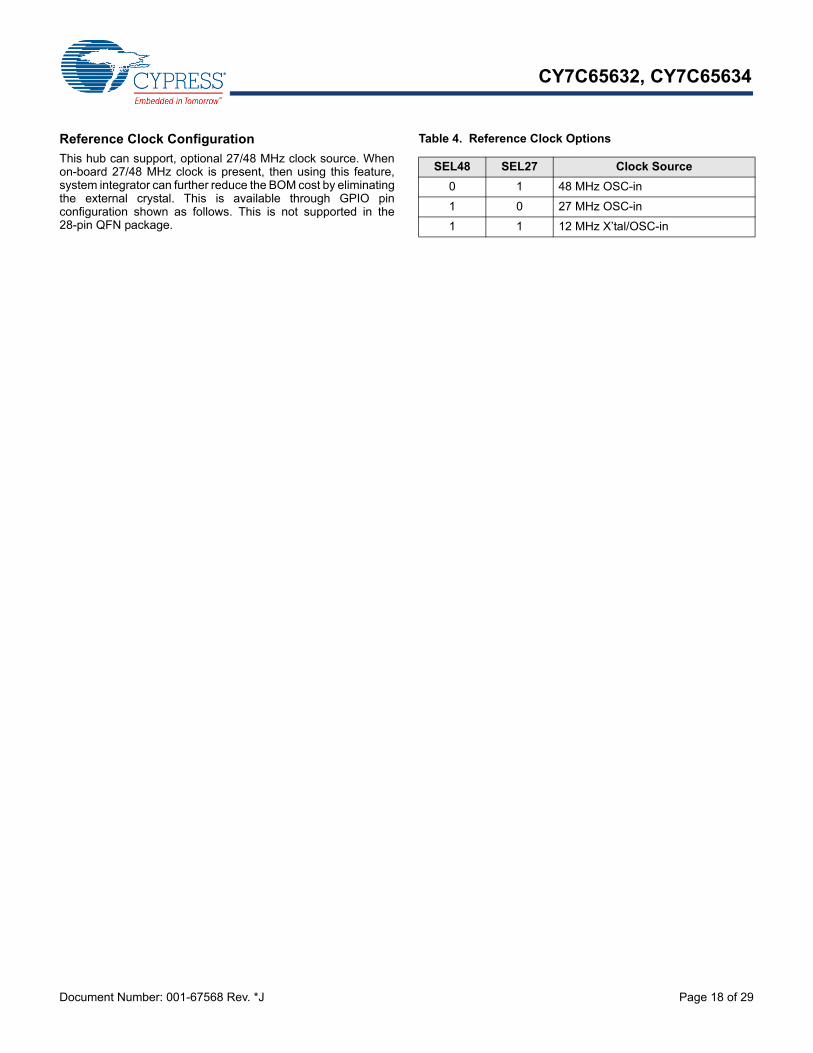
Reference Clock Configuration
This hub can support, optional 27/48 MHz clock source. Whenon-board 27/48 MHz clock is present, then using this feature,system integrator can further reduce the BOM cost by eliminatingthe external crystal. This is available through GPIO pinconfiguration shown as follows. This is not supported in the28-pin QFN package.
Table 4. Reference Clock Options
SEL48 SEL27 Clock Source
0 1 48 MHz OSC-in
1 0 27 MHz OSC-in
1 1 12 MHz X’tal/OSC-in
CY7C65632, CY7C65634
Document Number: 001-67568 Rev. *J Page 19 of 29
Absolute Maximum Ratings
Exceeding maximum ratings may shorten the useful life of thedevice. User guidelines are not tested.
Storage temperature ................................ –55 °C to +100 °C
Ambient temperature ..................................... 0 °C to +70 °C
5 V supply voltage to ground potential ........–0.5 V to +6.0 V
3.3 V supply voltage to ground potential .....–0.5 V to +3.6 V
Voltage at open drain input pins (OVR#1-4, SELFPWR, RESET#) ................–0.5 V to +5.5 V
3.3 V input voltage for digital I/O ..................–0.5 V to +3.6 V
FOSC (oscillator or crystal frequency) ........12 MHz ± 0.05%
Operating Conditions
Ambient temperature ..................................... 0 °C to +70 °C
Ambient max junction temperature .............. 0 °C to +125 °C
5 V supply voltage to ground potential ......4.75 V to +5.25 V
3.3 V supply voltage to ground potential .....3.15 V to +3.6 V
Input voltage for USB signal pins ..................0.5 V to +3.6 V
Voltage at open drain input pins ..................–0.5 V to +5.0 V
Thermal characteristics 48-pin TQFP ................... 78.7 °C/W
Thermal characteristics 28-pin QFN ..................... 33.3 °C/W
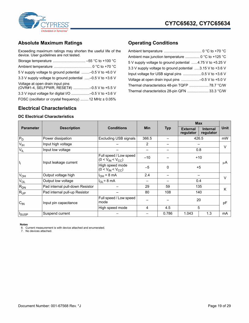
Electrical Characteristics
DC Electrical Characteristics
Parameter Description Conditions Min TypMax
UnitExternal regulator
Internal regulator
PD Power dissipation Excluding USB signals 366.5 – 426.5 mW
VIH Input high voltage – 2 – –V
VIL Input low voltage – – – 0.8
Il Input leakage current
Full speed / Low speed (0 < VIN < VCC) –10 – +10
AHigh speed mode (0 < VIN < VCC) –5 0 +5
VOH Output voltage high IOH = 8 mA 2.4 – –V
VOL Output low voltage IOL= 8 mA – – 0.4
RDN Pad internal pull-down Resistor – 29 59 135K
RUP Pad internal pull-up Resistor – 80 108 140
CIN Input pin capacitanceFull speed / Low speed mode
– – 20pF
High speed mode 4 4.5 5
ISUSP Suspend current – – 0.786 1.043 1.3 mA
Notes6. Current measurement is with device attached and enumerated.7. No devices attached.
CY7C65632, CY7C65634
Document Number: 001-67568 Rev. *J Page 20 of 29
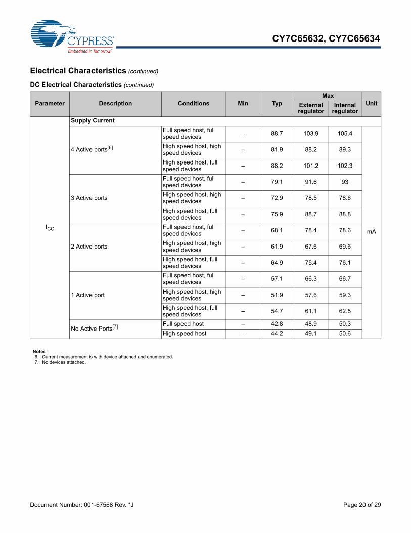
ICC
Supply Current
4 Active ports[6]
Full speed host, full speed devices – 88.7 103.9 105.4
mA
High speed host, high speed devices – 81.9 88.2 89.3
High speed host, full speed devices – 88.2 101.2 102.3
3 Active ports
Full speed host, full speed devices – 79.1 91.6 93
High speed host, high speed devices – 72.9 78.5 78.6
High speed host, full speed devices – 75.9 88.7 88.8
2 Active ports
Full speed host, full speed devices – 68.1 78.4 78.6
High speed host, high speed devices – 61.9 67.6 69.6
High speed host, full speed devices – 64.9 75.4 76.1
1 Active port
Full speed host, full speed devices – 57.1 66.3 66.7
High speed host, high speed devices – 51.9 57.6 59.3
High speed host, full speed devices – 54.7 61.1 62.5
No Active Ports[7] Full speed host – 42.8 48.9 50.3
High speed host – 44.2 49.1 50.6
Electrical Characteristics (continued)
DC Electrical Characteristics (continued)
Parameter Description Conditions Min TypMax
UnitExternal regulator
Internal regulator
Notes6. Current measurement is with device attached and enumerated.7. No devices attached.
CY7C65632, CY7C65634
Document Number: 001-67568 Rev. *J Page 21 of 29
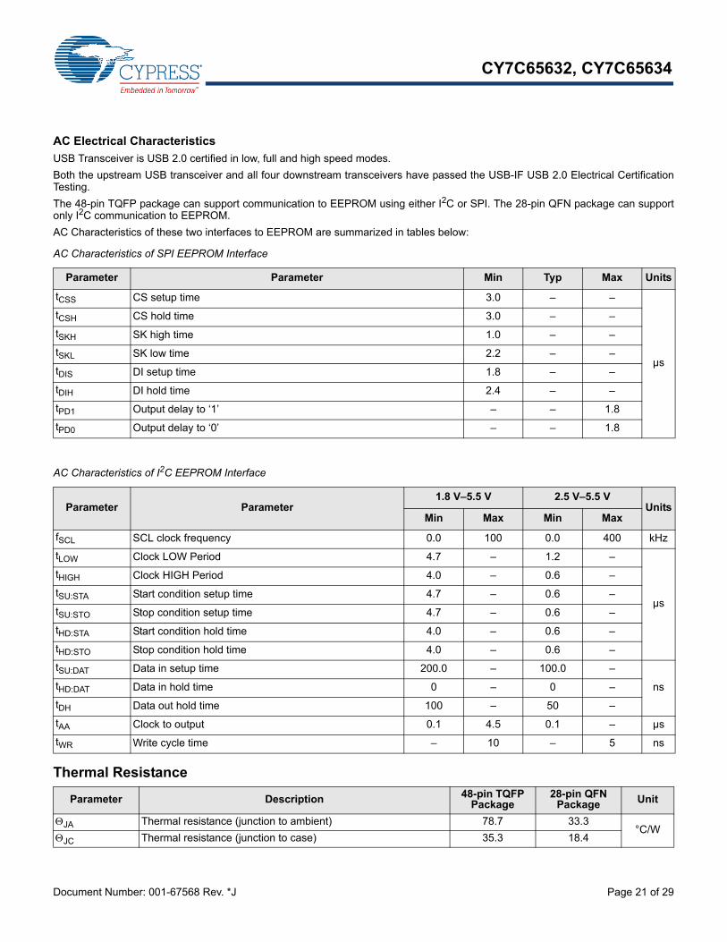
AC Electrical Characteristics
USB Transceiver is USB 2.0 certified in low, full and high speed modes.
Both the upstream USB transceiver and all four downstream transceivers have passed the USB-IF USB 2.0 Electrical CertificationTesting.
The 48-pin TQFP package can support communication to EEPROM using either I2C or SPI. The 28-pin QFN package can supportonly I2C communication to EEPROM.
AC Characteristics of these two interfaces to EEPROM are summarized in tables below:
AC Characteristics of SPI EEPROM Interface
Parameter Parameter Min Typ Max Units
tCSS CS setup time 3.0 – –
µs
tCSH CS hold time 3.0 – –
tSKH SK high time 1.0 – –
tSKL SK low time 2.2 – –
tDIS DI setup time 1.8 – –
tDIH DI hold time 2.4 – –
tPD1 Output delay to ‘1’ – – 1.8
tPD0 Output delay to ‘0’ – – 1.8
AC Characteristics of I2C EEPROM Interface
Parameter Parameter1.8 V–5.5 V 2.5 V–5.5 V
UnitsMin Max Min Max
fSCL SCL clock frequency 0.0 100 0.0 400 kHz
tLOW Clock LOW Period 4.7 – 1.2 –
µs
tHIGH Clock HIGH Period 4.0 – 0.6 –
tSU:STA Start condition setup time 4.7 – 0.6 –
tSU:STO Stop condition setup time 4.7 – 0.6 –
tHD:STA Start condition hold time 4.0 – 0.6 –
tHD:STO Stop condition hold time 4.0 – 0.6 –
tSU:DAT Data in setup time 200.0 – 100.0 –
nstHD:DAT Data in hold time 0 – 0 –
tDH Data out hold time 100 – 50 –
tAA Clock to output 0.1 4.5 0.1 – µs
tWR Write cycle time – 10 – 5 ns
Thermal Resistance
Parameter Description 48-pin TQFP Package
28-pin QFN Package Unit
JA Thermal resistance (junction to ambient) 78.7 33.3°C/W
JC Thermal resistance (junction to case) 35.3 18.4
CY7C65632, CY7C65634
Document Number: 001-67568 Rev. *J Page 22 of 29
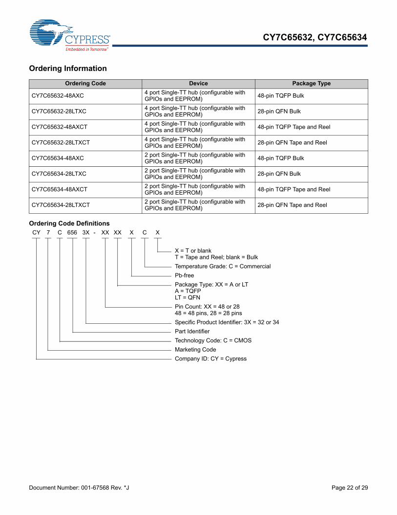
Ordering Information
Ordering Code Definitions
Ordering Code Device Package Type
CY7C65632-48AXC 4 port Single-TT hub (configurable with GPIOs and EEPROM)
48-pin TQFP Bulk
CY7C65632-28LTXC4 port Single-TT hub (configurable with GPIOs and EEPROM) 28-pin QFN Bulk
CY7C65632-48AXCT4 port Single-TT hub (configurable with GPIOs and EEPROM) 48-pin TQFP Tape and Reel
CY7C65632-28LTXCT4 port Single-TT hub (configurable with GPIOs and EEPROM) 28-pin QFN Tape and Reel
CY7C65634-48AXC2 port Single-TT hub (configurable with GPIOs and EEPROM) 48-pin TQFP Bulk
CY7C65634-28LTXC2 port Single-TT hub (configurable with GPIOs and EEPROM) 28-pin QFN Bulk
CY7C65634-48AXCT2 port Single-TT hub (configurable with GPIOs and EEPROM) 48-pin TQFP Tape and Reel
CY7C65634-28LTXCT2 port Single-TT hub (configurable with GPIOs and EEPROM) 28-pin QFN Tape and Reel
X = T or blank T = Tape and Reel; blank = Bulk
Temperature Grade: C = Commercial
Pb-free
Package Type: XX = A or LTA = TQFPLT = QFN
Pin Count: XX = 48 or 28 48 = 48 pins, 28 = 28 pins
Specific Product Identifier: 3X = 32 or 34
Part Identifier
Technology Code: C = CMOS
Marketing Code
Company ID: CY = Cypress
CCY 656 3X - XX XX7 X C X
CY7C65632, CY7C65634
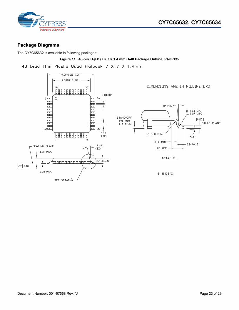
Document Number: 001-67568 Rev. *J Page 23 of 29
Package Diagrams
The CY7C65632 is available in following packages:
Figure 11. 48-pin TQFP (7 × 7 × 1.4 mm) A48 Package Outline, 51-85135
51-85135 *C
CY7C65632, CY7C65634
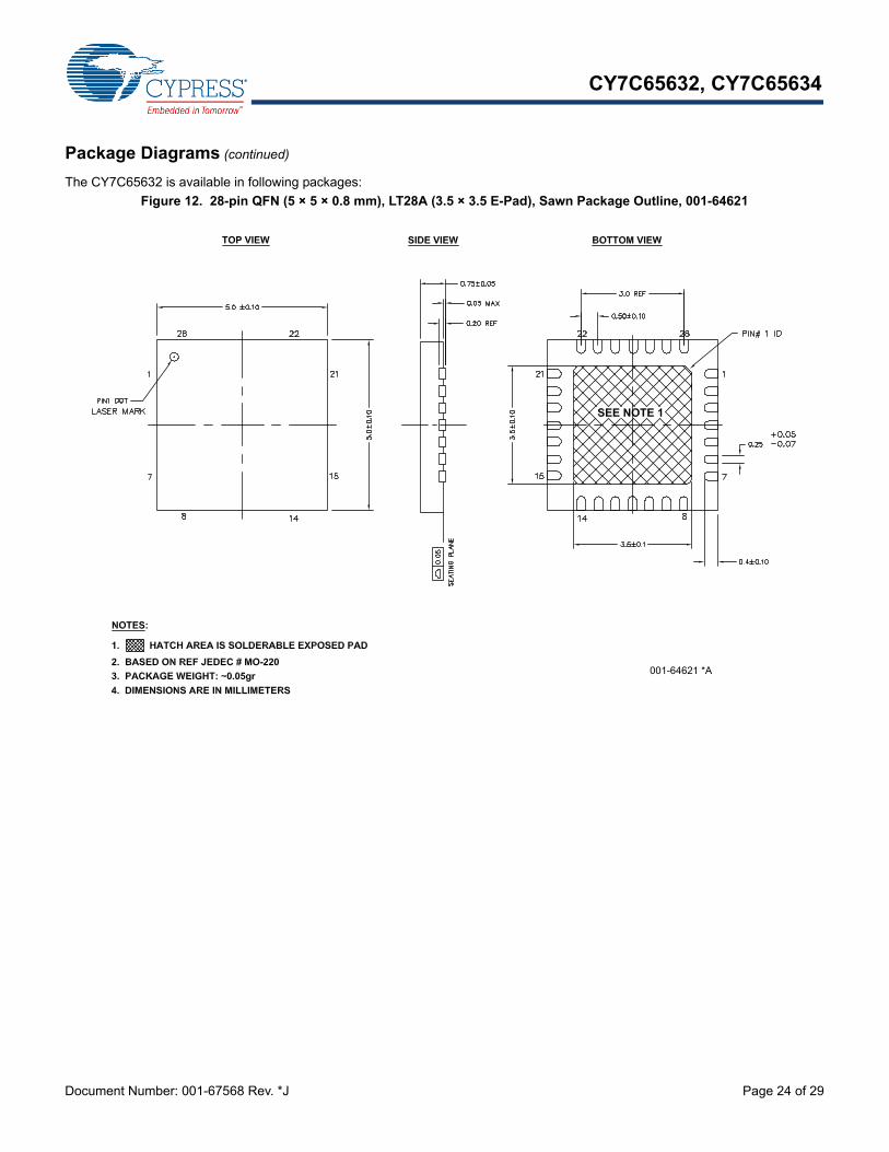
Document Number: 001-67568 Rev. *J Page 24 of 29
Figure 12. 28-pin QFN (5 × 5 × 0.8 mm), LT28A (3.5 × 3.5 E-Pad), Sawn Package Outline, 001-64621
Package Diagrams (continued)
The CY7C65632 is available in following packages:
001-64621 *A
CY7C65632, CY7C65634
Document Number: 001-67568 Rev. *J Page 25 of 29
Acronyms Document Conventions
Units of MeasureAcronym Description
AC alternating current
ASCII american standard code for information interchange
EEPROM electrically erasable programmable read only memory
EMI electromagnetic interference
ESD electrostatic discharge
GPIO general purpose input/output
I/O input/output
LED light emitting diode
LSB least significant bit
MSB most significant bit
PCB printed circuit board
PLL phase-locked loop
POR power on reset
PSoC® Programmable System-on-Chip™
QFN quad flat no leads
RAM random access memory
ROM read only memory
SIE serial interface engine
TQFP thin quad flat pack
TT transaction translator
USB universal serial bus
Symbol Unit of Measure
°C degree Celsius
kHz kilohertz
k kilohm
MHz megahertz
A microampere
s microsecond
W microwatt
mA milliampere
mm millimeter
ms millisecond
mW milliwatt
ns nanosecond
ohm
% percent
pF picofarad
ppm parts per million
V volt
W watt
CY7C65632, CY7C65634
Document Number: 001-67568 Rev. *J Page 26 of 29
Silicon Errata for the HX2VL, CY7C65632 Product Family
This section describes the errata for the HX2VL, CY7C65632. The details include errata trigger conditions, scope of impact, available workarounds, and silicon revision applicability.
Contact your local Cypress Sales Representative, if you have any questions.
Part Numbers Affected
HX2VL Qualification Status
Product Status: In production
HX2VL Errata Summary
This is the initial version of the HX2VL Errata. As of now, there is no known issue with respect to the HX2VL.
Part Number Device Characteristics
CY7C65632 USB 2.0 Single TT Hub
CY7C65632, CY7C65634
Document Number: 001-67568 Rev. *J Page 27 of 29
Document History Page
Document Title: CY7C65632/CY7C65634, HX2VL™ Very Low Power USB 2.0 Hub ControllerDocument Number: 001-67568
Revision ECN Orig. of Change
Submission Date Description of Change
** 3183649 SSJO / SWAK
03/02/2011 New data sheet.
*A 3250883 SWAK / AASI 05/06/2011
Updated Functional Overview (Updated Port Indicators (Added a Note“Pin-strapping GREEN#[1] and GREEN#[2] enables proprietary function thatmay affect the normal functionality of HX2VL. Configuring Port #1 and #2 asnon-removable by pin-strapping should be avoided.”).Updated Pin Configurations (Updated Figure 4 and Figure 5 (Pin 37 of the48-pin TQFP package was named SELF_PWR. It is changed to SELFPWR.)).Updated Pin Definitions (changed value from 680 to 650 in description ofRREF pin).Updated Functional Overview (Updated Power Regulator on page 6 (Changedregulator’s maximum current loading from 200 mA to 150 mA)).Updated Pin Configuration Options (Updated Power Switch Enable Pin Polarity(Replaced first two occurrences of the word “setting” with “pin-strapping”)).Updated Electrical Characteristics (Updated DC Electrical Characteristics(Changed typical value of ISUSP parameter from 693.3 µA to 786 µA, changedmaximum value of ISUSP parameter 693.7 µA to 903 µA, and updated typicaland maximum values of ICC parameter)).
*B 3324484 AASI 07/25/2011
Changed status from Preliminary to Final.Updated Pin Configurations (Included CY7C65634 related information).Updated Pin Definitions (Changed description of OVR# pins from “Default isActive LOW” to “Active LOW Overcurrent Condition Detection Input” (since thepolarity is not configurable)).Updated Pin Definitions (Changed description of OVR# pins from “Default isActive LOW” to “Active LOW Overcurrent Condition Detection Input” (since thepolarity is not configurable)).Updated Electrical Characteristics (Updated DC Electrical Characteristics(Updated minimum, typical, and maximum values of RDN and RUP parametersto 81 k103 k and 181 k)).
*C 3336689 SWAK 08/04/2011 No technical updates.
*D 3412885 AASI 10/18/2011
Updated Pin Configurations (Updated Figure 4 and Figure 5 (RenamedSPI_DI to SPI_MOSI, renamed SPI_DO to SPI_MISO respectively for clarity),updated Figure 6 (Updated pin 26 to describe the alternate functionI2C_SDA.), updated Figure 7 (Updated to reflect pin 20 as NC)).Updated Pin Definitions (Renamed SPI_DI to SPI_MOSI, renamed SPI_DOto SPI_MISO respectively for clarity).Updated Pin Definitions (Added Note 3 and referred the same note in PWR#).Minor text edits to add clarity.
*E 3508597 AASI 01/25/2011
Updated EEPROM Configuration Options (Removed text, “Strings must comply with the USB specification. The first byte (Byte 16) must be the length of the string in bytes, the second must be 0x03, and the string must be in ASCII code.” below “Vendor string”, “Product string” and “Serial Number string”.).Updated Functional Overview (Updated Overcurrent Detection (Included the text, “OVR#[n] has a setup time of 20 ns. It takes 3 to 4 ms from overcurrent detection to de-assertion of PWR#[n].”).
CY7C65632, CY7C65634
Document Number: 001-67568 Rev. *J Page 28 of 29
*F 3660597 AASI 07/02/2012
Updated EEPROM Configuration Options (Changed the value of Byte 5 toFEh to match with the tabular column).Updated Electrical Characteristics (Updated DC Electrical Characteristics(Splitted the Max column into two columns namely External regulator andInternal regulator for ISUSP and ICC parameters and updated the
corresponding values)).Added Thermal Resistance.Updated in new template.
*G 3995708 PRJI 05/09/2013 Added Silicon Errata for the HX2VL, CY7C65632 Product Family.
*H 4661191 PRJI 02/17/2015
Added More Information.Removed the note in Port Indicators.Updated the term “LOW” to “HIGH” in LED descriptions, in Pin Definitions asLEDs are active HIGH by default.Added Note 1 and 2, and referred it in Pin Definitions.Updated RDN and RDUP values in DC Electrical Characteristics.
Added Note 5 for GANG pin in DC Electrical Characteristics.Added Note 6 and 7 for Active ports and No active ports, and referred it in DCElectrical Characteristics.Updated Figure 11 (spec 51-85135 *B to *C) and Figure 12 (spec 001-64621** to *A) in Package Diagrams.Updated the Production Status “Sampling” to “In production” in HX2VLQualification Status.
*I 5363572 HBM 07/21/2016
Updated CY Logo and Sales Disclaimer.Updated Features: Added TID number along with Compliant with USB2.0specification. Removed Slew rate control for EMI management.Updated Pin Definitions for 28-pin QFN Package: Updated Description forOVR#[1], OVR#[2], OVR#[3], and OVR#[4].
*J 5545393 HBM 12/07/2016 Updated More Information.Updated Copyright and Disclaimer.
Document History Page (continued)
Document Title: CY7C65632/CY7C65634, HX2VL™ Very Low Power USB 2.0 Hub ControllerDocument Number: 001-67568
Revision ECN Orig. of Change
Submission Date Description of Change
Document Number: 001-67568 Rev. *J Revised December 7, 2016 Page 29 of 29
CY7C65632, CY7C65634
© Cypress Semiconductor Corporation, 2011-2016. This document is the property of Cypress Semiconductor Corporation and its subsidiaries, including Spansion LLC ("Cypress"). This document,including any software or firmware included or referenced in this document ("Software"), is owned by Cypress under the intellectual property laws and treaties of the United States and other countriesworldwide. Cypress reserves all rights under such laws and treaties and does not, except as specifically stated in this paragraph, grant any license under its patents, copyrights, trademarks, or otherintellectual property rights. If the Software is not accompanied by a license agreement and you do not otherwise have a written agreement with Cypress governing the use of the Software, then Cypresshereby grants you a personal, non-exclusive, nontransferable license (without the right to sublicense) (1) under its copyright rights in the Software (a) for Software provided in source code form, tomodify and reproduce the Software solely for use with Cypress hardware products, only internally within your organization, and (b) to distribute the Software in binary code form externally to end users(either directly or indirectly through resellers and distributors), solely for use on Cypress hardware product units, and (2) under those claims of Cypress's patents that are infringed by the Software (asprovided by Cypress, unmodified) to make, use, distribute, and import the Software solely for use with Cypress hardware products. Any other use, reproduction, modification, translation, or compilationof the Software is prohibited.
TO THE EXTENT PERMITTED BY APPLICABLE LAW, CYPRESS MAKES NO WARRANTY OF ANY KIND, EXPRESS OR IMPLIED, WITH REGARD TO THIS DOCUMENT OR ANY SOFTWAREOR ACCOMPANYING HARDWARE, INCLUDING, BUT NOT LIMITED TO, THE IMPLIED WARRANTIES OF MERCHANTABILITY AND FITNESS FOR A PARTICULAR PURPOSE. To the extentpermitted by applicable law, Cypress reserves the right to make changes to this document without further notice. Cypress does not assume any liability arising out of the application or use of anyproduct or circuit described in this document. Any information provided in this document, including any sample design information or programming code, is provided only for reference purposes. It isthe responsibility of the user of this document to properly design, program, and test the functionality and safety of any application made of this information and any resulting product. Cypress productsare not designed, intended, or authorized for use as critical components in systems designed or intended for the operation of weapons, weapons systems, nuclear installations, life-support devices orsystems, other medical devices or systems (including resuscitation equipment and surgical implants), pollution control or hazardous substances management, or other uses where the failure of thedevice or system could cause personal injury, death, or property damage ("Unintended Uses"). A critical component is any component of a device or system whose failure to perform can be reasonablyexpected to cause the failure of the device or system, or to affect its safety or effectiveness. Cypress is not liable, in whole or in part, and you shall and hereby do release Cypress from any claim,damage, or other liability arising from or related to all Unintended Uses of Cypress products. You shall indemnify and hold Cypress harmless from and against all claims, costs, damages, and otherliabilities, including claims for personal injury or death, arising from or related to any Unintended Uses of Cypress products.
Cypress, the Cypress logo, Spansion, the Spansion logo, and combinations thereof, WICED, PSoC, CapSense, EZ-USB, F-RAM, and Traveo are trademarks or registered trademarks of Cypress inthe United States and other countries. For a more complete list of Cypress trademarks, visit cypress.com. Other names and brands may be claimed as property of their respective owners.
Sales, Solutions, and Legal Information
Worldwide Sales and Design Support
Cypress maintains a worldwide network of offices, solution centers, manufacturer’s representatives, and distributors. To find the office closest to you, visit us at Cypress Locations.
Products
ARM® Cortex® Microcontrollers cypress.com/arm
Automotive cypress.com/automotive
Clocks & Buffers cypress.com/clocks
Interface cypress.com/interface
Internet of Things cypress.com/iot
Memory cypress.com/memory
Microcontrollers cypress.com/mcu
PSoC cypress.com/psoc
Power Management ICs cypress.com/pmic
Touch Sensing cypress.com/touch
USB Controllers cypress.com/usb
Wireless/RF cypress.com/wireless
PSoC® Solutions
PSoC 1 | PSoC 3 | PSoC 4 | PSoC 5LP
Cypress Developer Community
Forums | WICED IOT Forums | Projects | Video | Blogs | Training | Components
Technical Support
cypress.com/support