Embed Size (px)
Citation preview
01/08/15 Conexant Confidential • www.conexant.com 004-56DSR01
General DescriptionConexant's CX20756 is a low-power, 102dB Signal-to-Noise Ratio (SNR), High Definition (HD) audio Coder-Decoder (CODEC) that delivers high-quality audio for the mobile Personal Computer (PC) market, including notebooks, ultrabooks, and tablets.
Compliant with Intel's HD Audio Specification 1.0a, the CX20756 has audio fidelity that exceeds Microsoft desktop and notebook premium logo requirements, including Windows 8.x. The CX20756 includes two stereo Digital-to-Analog Converters (DACs) and Analog-to-Digital Converters (ADCs), a 2.8W stereo class-D, a capless headphone, an integrated headset, and digital microphones.
By combining these hardware features with Conexant's extensive voice and speech processing algorithms, the CODEC is the ideal solution for platforms that need Microsoft Lync, Skype, and Automatic Speech Recognition (ASR) certification.
Applications• Notebooks• Ultrabooks• Desktop and all-in-one PCs• Tablets• Embedded applications
System Compatibility• HD Audio Specification 1.0a• Windows XP/Vista/7/8.x• Microsoft Premium Logo• Linux • Android
Features• Two pairs of independent DACs and ADCs• Independent sampling rates for DACs and ADCs—
supports audio formats ranging from 16-bit to 24-bit, 44.1kHz to 192kHz for DAC, and 44.1kHz to 96kHz for ADC
• 2.8WRMS per channel class-D stereo speaker amplifier with spread spectrum
• SpeakerShield technology provides load-based speaker protection independent of driver and OS—Protection includes Direct Current (DC), short, near-short, and temperature
• ProCoustic capless stereo headphone driver delivers 32mW into 32 load with no pops
• Built-in four-conductor headset jack support with in-line command sensing
• Hum noise is prevented on external powered speakers plugged into the headset jack when the system is off
• Universal jack supports headsets, headphones, external microphones, and external line-in devices
• Digital Microphone Interface (DMIC) with boost supporting two digital microphone elements and DC offset removal
• Record security prevents unwanted recordings from all or selected input ports
• Analog and digital PC Beep are supported, and Wake-on-beep never misses a beep—even when in low-power mode
• Multiple General Purpose Input/Outputs (GPIOs) for custom applications
• Integrated Low Drop-Out (LDO) regulators• Headphone limiter supports GS Mark EN50332-2
without an external Bill Of Materials (BOM)
CX20756 Low-Power High Definition Audio CODECData Sheet
CX20756 Data Sheet Revision History
Conexant Confidential01/08/15 004-56DSR01 ii
Revision HistoryDocument No. Release Date Change Description004-56DSR01 01/08/15 Added 1.8V HD link signaling support.
004-56DSR00 08/05/14 Initial release.
CX20756 Data Sheet Table of Contents
Table of ContentsGeneral Description.......................................................................................................................................................iApplications ...................................................................................................................................................................iSystem Compatibility ....................................................................................................................................................iFeatures..........................................................................................................................................................................i
Revision History ...........................................................................................................................................................iiIntroduction...................................................................................................................................................................1
Overview............................................................................................................................................................................... 1
CX20756 Audio CODEC Features....................................................................................................................................... 2
System Compatibility .......................................................................................................................................................... 3
Hardware Qualification Process (HQP).............................................................................................................................. 3
Hardware Interface .......................................................................................................................................................4General ................................................................................................................................................................................. 4
High Definition (HD) Audio Host Interface .................................................................................................................. 4
Control Signals ........................................................................................................................................................... 4
Audio Signals.............................................................................................................................................................. 4
CX20756 Block Diagram...................................................................................................................................................... 5
Pin Assignments and Signal Definitions........................................................................................................................... 6
Absolute Maximum Ratings.............................................................................................................................................. 12
Electrical Characteristics.................................................................................................................................................. 13
Device Performance Specifications................................................................................................................................. 14
Power Management and Power Consumption................................................................................................................ 17
Power Management.................................................................................................................................................. 17
Power Supply Minimum/Maximum Ratings .............................................................................................................. 17
Power Consumption ................................................................................................................................................. 18
Integrated Low Drop-Out (LDO) Regulators ............................................................................................................. 19
Digital High-Pass Filter (HPF)................................................................................................................................... 20
Alternating Current (AC) Timing Characteristics............................................................................................................ 21
Digital Microphone Interface (DMIC) ........................................................................................................................ 21
HD Audio Clocks....................................................................................................................................................... 22
Data Output and Input .............................................................................................................................................. 23
Package Dimensions and Thermal Specifications ......................................................................................................... 24
HD Audio Interface......................................................................................................................................................26Overview............................................................................................................................................................................. 26
Conexant Confidential01/08/15 004-56DSR01 iii

CX20756 Data Sheet Table of Contents
Verbs................................................................................................................................................................................... 27
Node ID 00: Root Node ............................................................................................................................................ 28
Node ID 01: Audio Function Group (AFG)................................................................................................................ 29
Nodes 10, 11: DAC 1, 2 Widgets.............................................................................................................................. 31
Node 12: PC Beep Generator Widget ...................................................................................................................... 32
Node 13, 14: ADC 1, 2 Widget ................................................................................................................................. 33
Node 15: Mixer Widget ............................................................................................................................................. 35
Node 16: Port A/Vendor Widget ............................................................................................................................... 36
Node 17: Port G........................................................................................................................................................ 37
Node 18: Port B Widget ............................................................................................................................................ 38
Node 19: Port D Widget............................................................................................................................................ 40
Node 1A: Port C Widget ........................................................................................................................................... 41
Ordering Information..................................................................................................................................................42
Conexant Confidential01/08/15 004-56DSR01 iv
CX20756 Data Sheet List of Figures
Conexant Confidential01/08/15 004-56DSR01 V
List of FiguresFigure 1: CX20756 Block Diagram ................................................................................................................................................... 5
Figure 2: CX20756 40-QFN Hardware Interface Signals.................................................................................................................. 6
Figure 3: CX20756 40-QFN Pad Signals.......................................................................................................................................... 7
Figure 4: Power Supply Rejection for Class-D Amplifier Output..................................................................................................... 15
Figure 5: Power Supply Rejection for Headphone Amplifier Output ............................................................................................... 15
Figure 6: Class-D Output Power vs Load (1% THD) ...................................................................................................................... 16
Figure 7: HPF Response ................................................................................................................................................................ 20
Figure 8: Digital Microphone Clock Timing Waveform.................................................................................................................... 21
Figure 9: BIT_CLK and SYNC Timing Waveforms ......................................................................................................................... 22
Figure 10: Data Output and Input Timing Waveforms .................................................................................................................... 23
Figure 11: CX20756 40-QFN Package Drawing............................................................................................................................. 24

CX20756 Data Sheet List of Tables
Conexant Confidential01/08/15 004-56DSR01 VI
List of TablesTable 1: CX20756 Pad Signals......................................................................................................................................................... 8
Table 2: Pad Signal Definitions......................................................................................................................................................... 9
Table 3: Absolute Maximum Ratings .............................................................................................................................................. 12
Table 4: DC Characteristics—Digital Microphone........................................................................................................................... 13
Table 5: DC Characteristics—TTL Compatible (GPIOs, SPKR_MUTE#, and MUSIC_REQ) ........................................................ 13
Table 6: Analog Performance Characteristics ................................................................................................................................ 14
Table 7: Device Power State Mapping............................................................................................................................................ 17
Table 8: DC Supply Voltages.......................................................................................................................................................... 17
Table 9: AFG D3 Power Consumption............................................................................................................................................ 18
Table 10: Full Scale Headphone Playback (32 Load) ................................................................................................................. 18
Table 11: Full Scale Class-D Playback (1W per Channel) ............................................................................................................. 18
Table 12: Line-In Recording............................................................................................................................................................ 19
Table 13: Digital Microphone Timing Parameters........................................................................................................................... 21
Table 14: BIT_CLK and SYNC Timing Parameters ........................................................................................................................ 22
Table 15: HD Audio Output Valid Delay Timing Parameters .......................................................................................................... 23
Table 16: HD Audio Input Setup and Hold Timing Parameters ...................................................................................................... 23
Table 17: Thermal Specifications.................................................................................................................................................... 25
Table 18: Node 0 Responses ......................................................................................................................................................... 28
Table 19: Node 01 Responses ....................................................................................................................................................... 29
Table 20: Node 10 and 11 Responses ........................................................................................................................................... 31
Table 21: PC Beep Generator Responses ..................................................................................................................................... 32
Table 22: Node 13 and 14 Responses ........................................................................................................................................... 33
Table 23: Node 15 Responses ...................................................................................................................................................... 35
Table 24: Node 16 Responses ....................................................................................................................................................... 36
Table 25: Node 17 Responses ....................................................................................................................................................... 37
Table 26: Node 18 Response ......................................................................................................................................................... 38
Table 27: Node 19 Response ......................................................................................................................................................... 40
Table 28: Node 1A Responses ....................................................................................................................................................... 41
Table 29: CX20756 Ordering Information and Functions ............................................................................................................... 42
CX20756 Data Sheet Introduction
Introduction
OverviewConexant's CX20756 is a low-power, 102dB SNR, HD audio CODEC that delivers high-quality audio for the mobile PC market, including notebooks, ultrabooks, and tablets.
Compliant with Intel's HD Audio Specification 1.0a, the CX20756 has audio fidelity that exceeds Microsoft desktop and notebook premium logo requirements, including Windows 8.x. With two 24-bit stereo DACs that operate at sampling frequencies up to 192kHz and two 24-bit stereo ADCs that operate at sampling frequencies up to 96kHz, the CODEC can support multi-streaming and RTC applications. By combining these hardware features with Conexant's extensive voice and speech processing algorithms, the CODEC is the ideal solution for platforms that need Microsoft Lync, Skype, and ASR certification.
The CX20756 has an integrated stereo filterless class-D amplifier with a HPF and patented common mode scrambling technology that is capable of driving 2.8WRMS per channel into a 4 load. Devices and speakers have load-based protection, including DC detection, short-circuit, over-current, and over-temperature.
The tri-state, ProCoustic capless headphone driver produces a full-range frequency response and eliminates external Field Effect Transistors (FETs) for supporting a headset jack. In-line command sensing enables control of third-party applications directly from the headset.
A single jack supports fixed-type headsets, headphones, external microphones, and line-in devices. A Pulse Density Modulated (PDM) single-bit stream interface supports two digital microphones with DC offset removal for array implementations.
Conexant's PopShield technology eliminates pops and clicks during all transition states, and includes active DC offset removal and an innovative Voltage reference (Vref) ramping scheme. The CX20756 has D-Flex power management that exceeds Intel's ECR 15B requirements and consumes minimum power during connected standby by powering down DACs, ADCs, and amplifiers without pops or clicks.
Conexant offers comprehensive audio software driver support, with both in-house and third-party software APOs, including Andrea Electronics, Creative Labs, Dolby, DTS, Sonic Focus, MaxxAudio, Waves, and more. Conexant’s AudioSmart voice and speech processing algorithm suite ensures clear voice communication and speech command and control in noisy environments. The Smart Source Pickup (SSP) does not use or rely on beam-forming techniques, and provides an easy to use powerful solution that requires few or no user controls. The SSP passes the latest Intel ASR certification in all orientations with just two microphones, and is available for Windows, Linux, and Android. AudioSmart also offers keystroke, screen tapping, and fan noise suppression.
Conexant Confidential01/08/15 004-56DSR01 1

CX20756 Data Sheet CX20756 Audio CODEC Features
CX20756 Audio CODEC FeaturesThe following lists the CX20756 audio CODEC features:
• Two pairs of independent DACs and ADCs• Independent sampling rates for DACs and ADCs—Supports audio formats ranging from 16-bit to 24-
bit, 44.1kHz to 192kHz for DAC, and 44.1kHz to 96kHz for ADC• 2.8WRMS per channel class-D stereo speaker amplifier with spread spectrum
• SpeakerShield technology provides load-based speaker protection independent of driver and application—Protection includes DC, short, near-short, and temperature
• ProCoustic capless stereo headphone driver delivers 32mW into 32 load with no pops• Built-in four-conductor headset jack support with in-line command sensing• Hum noise is prevented on external powered speakers plugged into the headset jack when the system
is off• One jack supports fixed headsets, headphones, external microphones, and external line-in devices• DMIC with boost supports two digital microphone elements and DC offset removal• Record security prevents unwanted recordings from all or selected input ports• Analog and digital PC Beep are supported, and Wake-on-beep never misses a beep—even when in
low-power mode• Multiple GPIOs for custom applications• Speaker mute control input selectively mutes the class-D outputs• Integrated LDO regulators• Headphone limiter supports GS Mark EN50332-2 without an external BOM• Integrated:
– 5V to 3.3V LDO voltage regulator for improved analog audio performance– 3.3V to 1.8V LDO voltage regulator used to power digital blocks
• 1.5V, 1.8V and 3.3V HD audio link signaling levels are selectable• Pop Shield II for enhanced pop and click suppression• Jack sense detects jack events as well as enabling hardware-only selections for class-D mono mode
and port C mono mode without Basic Input/Output System (BIOS) intervention• An integrated digital mixer is used to record what is playing• D-Flex enhanced power management exceeds Intel ECR 15B requirements• Compliant with Intel’s HD Audio Specification 1.0a, and fidelity exceeds Vista/Windows 7/Windows 8.x
desktop and notebook Premium Logo requirements• AudioSmart super wideband voice and speech processing algorithms are available:
– End-to-end noise reduction – True stereo Acoustic Echo Cancellation (AEC)– SSP– Far Field Pickup– ASR certification for all form factors and orientations with two microphones
• Keystroke, screen tap, and fan noise suppression• 10-band digital parametric SmartEQ enhances the sound quality on low-cost speakers• Night mode boosts vocal clarity while maintaining background sound quality• Multi-band DRC further improves the sound quality and loudness of low-cost speakers and prevents
speaker rattle and distortion
Conexant Confidential01/08/15 004-56DSR01 2
CX20756 Data Sheet System Compatibility
• Phantom bass creates virtual bass content on mainstream speakers• 3D:
– Expander widens the audio stage for fuller and richer sound– Headphone recreates a surround, speaker-like environment in headphones so users can enjoy a
richer, fuller music listening experience • AudioSmart™ GUI—Advanced audio control panel• Audio director for classic and multi-stream selections• Third-party software support includes:
– DTS, Inc.– Dolby– Creative Labs– ForteMedia– Andrea– Waves (MaxxAudio)
• Supports 32-bit/64-bit Windows OS and Linux• Available in a 40-pad, thermally-enhanced Quad Flat No-leads (QFN) package
System Compatibility• HD Audio Specification 1.0a• Windows XP/Vista/7/8.x• Microsoft Premium Logo• Linux • Android
Hardware Qualification Process (HQP)The Hardware Qualification Process (HQP) is intended to improve the quality and reliability of board designs using the CX20756. The goals of this process are to:
• Eliminate common design mistakes• Ensure boards perform well and pass Driver Test Manager (DTM) fidelity requirements with good
margin• Eliminate potential manufacturing issues that may result from a marginal design• Eliminate country-specific issues• Eliminate INF problems• Converge towards standard designs
The HQP process includes review of schematics, board layout, and BOM. All boards must meet the pre-defined criteria. Contact the local Conexant sales office for more details about the HQP process. The HQP process must be performed for all Original Equipment Manufacturer (OEM) designs.
Conexant Confidential01/08/15 004-56DSR01 3

CX20756 Data Sheet Hardware Interface
Hardware Interface
General
High Definition (HD) Audio Host InterfaceThe HD audio host interface conforms to Intel's HD Audio Specification 1.0a. The following lists the supported HD audio signals:
• Bit clock (BIT_CLK), input• Frame sync (SYNC), input• Serial data output (SDATA_OUT), input• Serial data input (SDATA_IN), input/output• Master hardware reset (RESET#), input
Control SignalsThe following lists the control signals that are supported from straps or the host:
• Class-D speaker mute (SPKR_MUTE#), input• Jack sense (JSENSE), input• GPIOs (GPIO0, GPIO1)
Audio SignalsThe following lists the supported audio interface signals:
• Port A (PORTA_L and PORTA_R), ProCoustic headphone output/line output, headset• Port B (PORTB_L and PORTB_R), microphone input/line input with Microphone Bias (micbias) voltage• Port C (PORTC_L and PORTC_R), analog or digital microphone input with micbias voltage• Port D (PORTD_MIC), analog headset mono microphone input• Port G (LEFT+ and RIGHT+), class-D speaker amplifier stereo/mono output• PC Speaker Beep pass-through (PC_BEEP), input
Conexant Confidential01/08/15 004-56DSR01 4
CX20756 Data Sheet CX20756 Block Diagram
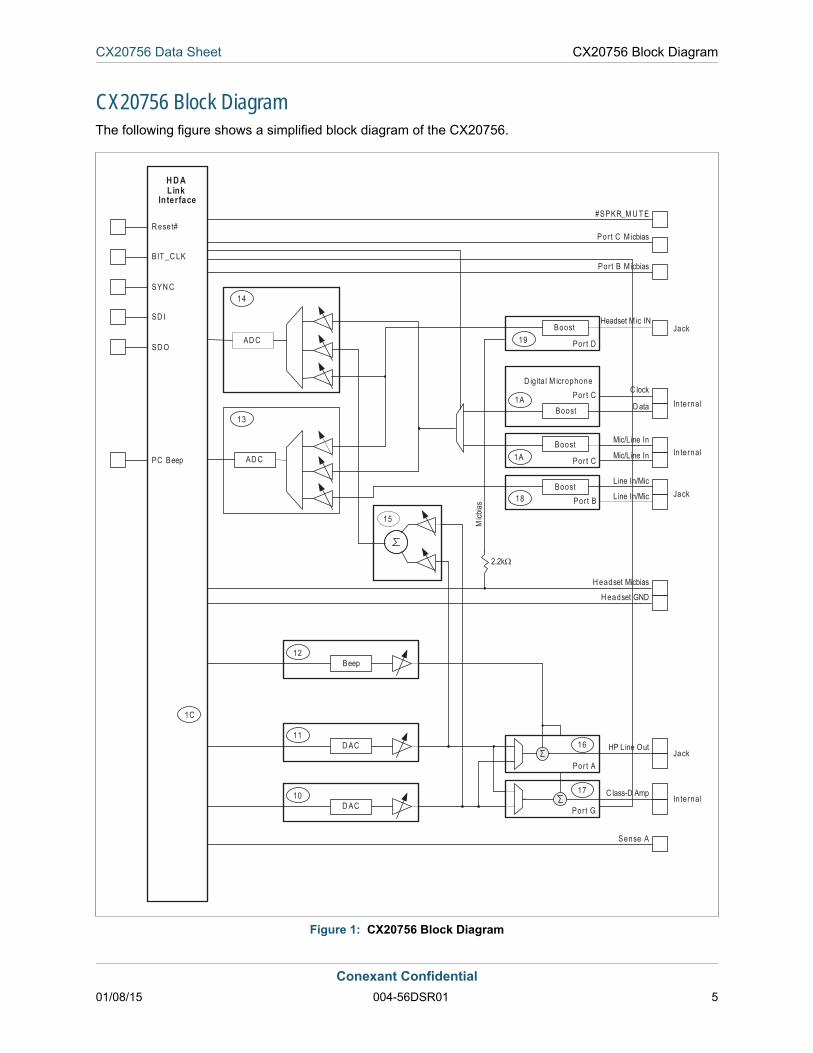
CX20756 Block DiagramThe following figure shows a simplified block diagram of the CX20756.
Figure 1: CX20756 Block Diagram
H D ALink
Interface
R eset#
BIT _C LK
SYN C
SD I
SD O
C lockD ig ita l M icrophone
1A
18
Mic/L ine In
Por t B M icbias
Port C
Port B
D AC11
17
Port G
16
Port A
HP Line Out
C lass-D Amp
PC Beep
D ata1A Port C
Boost
D AC10
Beep12
H eadset Micbias
AD C
13
Boost
BoostJack
Internal
Jack
Internal
AD C
14
15
1C
Port C M icbias
Sense A
Internal
#SPKR_M U T E
19
Headset M ic INBoost Jack
Micb
ias
H eadset GND
2.2kΩ
Port D
Mic/L ine In
L ine In/Mic
Line In/Mic
Conexant Confidential01/08/15 004-56DSR01 5
CX20756 Data Sheet Pin Assignments and Signal Definitions
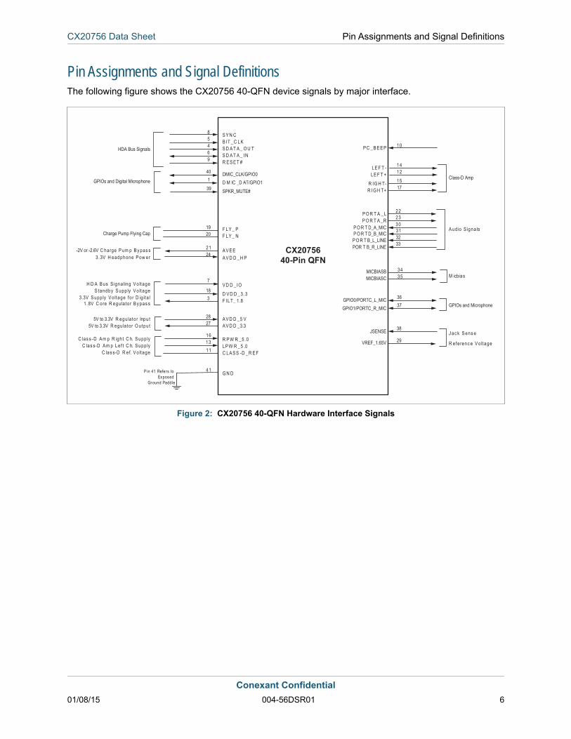
Pin Assignments and Signal DefinitionsThe following figure shows the CX20756 40-QFN device signals by major interface.
Figure 2: CX20756 40-QFN Hardware Interface Signals
P C _B E E P
LE F T -LE F T +
R IG H T-R IG H T+
MICBIASB MICBIASC
Class-D Amp
VREF_1.65V
10
1412
1517
3435
38
29
S Y N CB IT _C LKS D A T A _ O U TS D A T A _ INR E S E T #
DMIC_CLK/GPIO0D M IC _D AT/GPIO1
F LY _ PF LY _ N
A V E EA V D D _H P
V D D _IO
D V D D _3.3F ILT_ 1.8
A V D D _5 VA V D D _3.3
R P W R _5.0LP W R _5 .0C LA S S -D _R E F
G N D
85469
1920
2124
7
183
2827
16
11
41
R eferenc e V o ltage
M icbias
J ac k S ens e
Pin 41 Refers to Exposed
Ground Paddle
CX2075640-Pin QFN
SPKR_MUTE#
GPIO0/PORTC_L_MICGPIO1/PORTC_R_MIC
401
3637
39
P O R T A _LP O R T A _R
P O R T D_A_MIC
222330
A ud io S igna ls
P O R T B_L_LINEPOR T B_R_LINE
3233
13
JSENSE
P O R T D_B_MIC 31
H D A B us S igna ling V o ltageS tandby S upp ly V o ltage
3.3V S upp ly V o ltage fo r D ig ita l1 .8V C ore R egu la to r B y pas s
-2V or -2.6V C harge Pum p By pas s3.3V H eadphone Pow er
5V to 3.3V R egu la to r O utpu t
C las s -D A m p R igh t C h. S upp lyC las s-D A m p Lef t C h. S upp ly
C las s-D R ef. V o ltage
Charge Pump Flying Cap
HDA Bus Signals
GPIOs and Digital Microphone
5V to 3.3V R egu la to r Inpu t
GPIOs and Microphone
Conexant Confidential01/08/15 004-56DSR01 6
CX20756 Data Sheet Pin Assignments and Signal Definitions
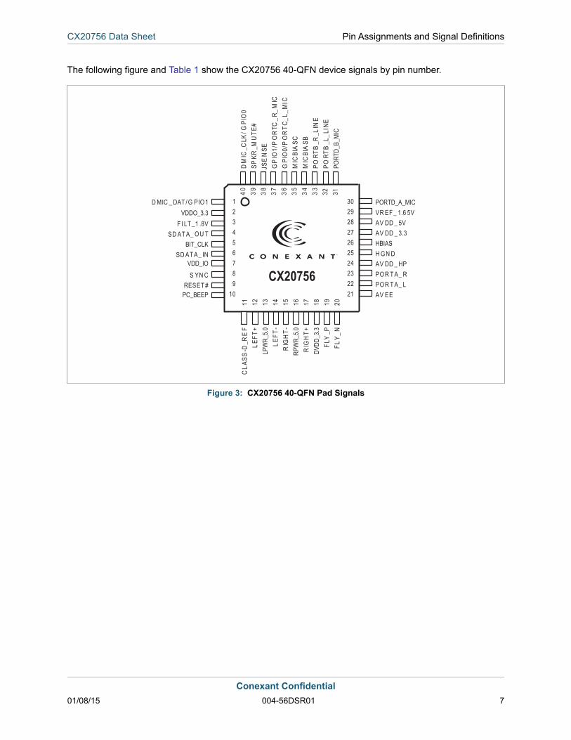
The following figure and Table 1 show the CX20756 40-QFN device signals by pin number.
Figure 3: CX20756 40-QFN Pad Signals
123456789
10
11 12 13 14 15 16 17 18 19 20
40 39 38 37 36 35 34 33 32 31
D MIC _ DAT / G PIO1
F I LT _1 .8VSD AT A_ OU T
BIT_CLKSD AT A_ IN
S YN CRESET #
PORTD_A_MICVR EF _ 1.6 5VAV DD _ 5VAV DD _ 3.3HBIASH GN DAV DD _ HPPOR T A_ RPOR T A_ LAV EE
DM
IC_C
LK/ G
PIO
0SP
KR_M
UTE
#JS
EN
SEG
PIO
1 / P
OR
TC_R
_MIC
C
GPI
O0 /
PO
RTC
_L_M
IM
ICBI
ASC
MIC
BIA
SBPO
RTB
_R_L
INE
PORT
B_L
_LIN
EPO
RTD_
B_MI
C
CLA
SS-D
_RE
FLE
FT+
LPW
R_5.0
LEFT
-R
IGH
T-RP
WR_
5.0R
IGH
T+DV
DD_3
.3FL
Y_P
FLY_
N
30292827262524232221
CX20756
VDDO_3.3
VDD_IO
PC_BEEP
Conexant Confidential01/08/15 004-56DSR01 7
CX20756 Data Sheet Pin Assignments and Signal Definitions
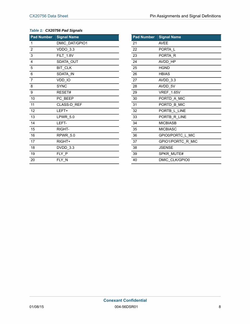
Table 1: CX20756 Pad Signals
Pad Number Signal Name Pad Number Signal Name1 DMIC_DAT/GPIO1 21 AVEE
2 VDDO_3.3 22 PORTA_L
3 FILT_1.8V 23 PORTA_R
4 SDATA_OUT 24 AVDD_HP
5 BIT_CLK 25 HGND
6 SDATA_IN 26 HBIAS
7 VDD_IO 27 AVDD_3.3
8 SYNC 28 AVDD_5V
9 RESET# 29 VREF_1.65V
10 PC_BEEP 30 PORTD_A_MIC
11 CLASS-D_REF 31 PORTD_B_MIC
12 LEFT+ 32 PORTB_L_LINE
13 LPWR_5.0 33 PORTB_R_LINE
14 LEFT- 34 MICBIASB
15 RIGHT- 35 MICBIASC
16 RPWR_5.0 36 GPIO0/PORTC_L_MIC
17 RIGHT+ 37 GPIO1/PORTC_R_MIC
18 DVDD_3.3 38 JSENSE
19 FLY_P 39 SPKR_MUTE#
20 FLY_N 40 DMIC_CLK/GPIO0
Conexant Confidential01/08/15 004-56DSR01 8

CX20756 Data Sheet Pin Assignments and Signal Definitions
The following lists the acronyms used in Table 2:
Table 2: Pad Signal Definitions
• GND = Ground• I = Input• Ia = Input analog• Id = In Digital• IHD = Input High Definition
• O = Output• Oa = Output analog• Od = Out digital• PWR = Power• Ref = Reference
Label Pad Number Type I/O
Type Signal Name/Description
PowerVDD0_3.3 2 PWR I Digital Supply Voltage. 3.3V—Connect to the 3.3V system.
FILT_1.8V 3 PWR O Internally Regulated Digital Core Supply Voltage. 1.8V –5%/10%—Connect to an external decoupling capacitor.
VDD_IO 7 PWR I Input/Output Signaling Voltage Supply. Determines the signaling voltage that is being used on the host system. When VDD_IO is:• 1.5V, the device uses 1.5V signaling on the HDA interface
pins• 1.8V, the device uses 1.8V signaling on the HDA interface
pins• 3.3V, the device uses 3.3V signaling on the HDA interface
pins
LPWR_5.0 13 PWR I Supply Voltage for Class-D Amplifier, Left Channel. 5V—Connect to RPWR_5.0. Connect LPWR_5.0/RPWR_5.0, and then to the 5V system supply.
RPWR_5.0 16 PWR I Supply Voltage for Class-D Amplifier, Right Channel. 5V—Connect to LPWR_5.0. Connect LPWR_5.0/RPWR_5.0, and then to the 5V system supply.
DVDD_3.3 18 PWR I Charge Pump Input Supply Voltage. 3.3V—Connect to the 3.3V system.
FLY_P 19 PWR Ref Charge Pump Negative Transfer Charge. Connected to FLY_N through a 1μF capacitor.
FLY_N 20 PWR Ref Charge Pump Negative Transfer Charge. Connected to FLY_P through a 1μF capacitor.
AVEE 21 PWR O Internally Generated Analog Negative Supply. –2.0V –10%/15%—Connect to an external decoupling capacitor.
AVDD_HP 24 PWR I Supply Input Voltage for Headphone Amplifiers. 3.3V—Connect to the 3.3V system.
AVDD_3.3 27 PWR O Output Voltage from LDO. 3.3V –5%/10%—Connect to an external decoupling capacitor.
AVDD_5V 28 PWR I Analog Supply Input Voltage for LDO. 5V—Connect to the 5V system supply.
Ground (GND)HGND 25 GND GND Headset Ground: Ground sense for headsets.
GND 41 GND GND CODEC Ground. Thermal/electrical GND paddle of the device. Connect to the system and audio ground.
Conexant Confidential01/08/15 004-56DSR01 9
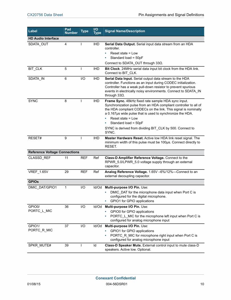
CX20756 Data Sheet Pin Assignments and Signal Definitions
HD Audio InterfaceSDATA_OUT 4 I IHD Serial Data Output. Serial input data stream from an HDA
controller. • Reset state = Low• Standard load = 50pFConnect to SDATA_OUT through 33Ω.
BIT_CLK 5 I IHD Bit Clock. 24MHz serial data input bit clock from the HDA link. Connect to BIT_CLK.
SDATA_IN 6 I/O IHD Serial Data Input. Serial output data stream to the HDA controller. Functions as an input during CODEC initialization. Controller has a weak pull-down resistor to prevent spurious events in electrically noisy environments. Connect to SDATA_IN through 33Ω.
SYNC 8 I IHD Frame Sync. 48kHz fixed rate sample HDA sync input. Synchronization pulse from an HDA compliant controller to all of the HDA compliant CODECs on the link. This signal is nominally a 0.167μs wide pulse that is used to synchronize the HDA. • Reset state = Low• Standard load = 50pFSYNC is derived from dividing BIT_CLK by 500. Connect to SYNC.
RESET# 9 I IHD Master Hardware Reset. Active low HDA link reset signal. The minimum width of this pulse must be 100μs. Connect directly to RESET.
Reference Voltage ConnectionsCLASSD_REF 11 REF Ref Class-D Amplifier Reference Voltage. Connect to the
RPWR_5.0/LPWR_5.0 voltage supply through an external capacitor.
VREF_1.65V 29 REF Ref Analog Reference Voltage. 1.65V –6%/12%—Connect to an external decoupling capacitor.
GPIOsDMIC_DAT/GPIO1 1 I/O Id/Od Multi-purpose I/O Pin. Use:
• DMIC_DAT for the microphone data input when Port C is configured for the digital microphone.
• GPIO1 for GPIO applications
GPIO0/ PORTC_L_MIC
36 I/O Id/Od Multi-purpose I/O Pin. Use:• GPIO0 for GPIO applications• PORTC_L_MIC for the microphone left input when Port C is
configured for analog microphone input
GPIO1/ PORTC_R_MIC
37 I/O Id/Od Multi-purpose I/O Pin. Use:• GPIO1 for GPIO applications• PORTC_R_MIC for microphone right input when Port C is
configured for analog microphone input
SPKR_MUTE# 39 I Id Class-D Speaker Mute. External control input to mute class-D speakers. Active low. Optional.
Label Pad Number Type I/O
Type Signal Name/Description
Conexant Confidential01/08/15 004-56DSR01 10
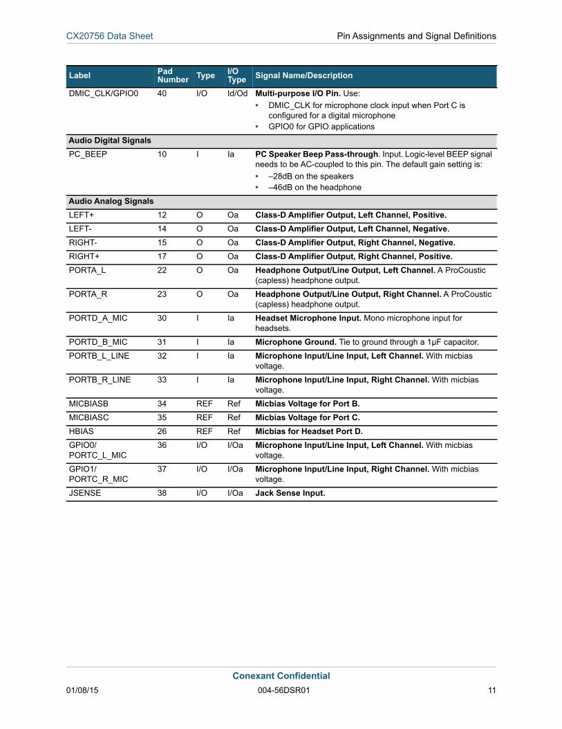
CX20756 Data Sheet Pin Assignments and Signal Definitions
DMIC_CLK/GPIO0 40 I/O Id/Od Multi-purpose I/O Pin. Use:• DMIC_CLK for microphone clock input when Port C is
configured for a digital microphone• GPIO0 for GPIO applications
Audio Digital SignalsPC_BEEP 10 I Ia PC Speaker Beep Pass-through. Input. Logic-level BEEP signal
needs to be AC-coupled to this pin. The default gain setting is:• –28dB on the speakers• –46dB on the headphone
Audio Analog SignalsLEFT+ 12 O Oa Class-D Amplifier Output, Left Channel, Positive. LEFT- 14 O Oa Class-D Amplifier Output, Left Channel, Negative. RIGHT- 15 O Oa Class-D Amplifier Output, Right Channel, Negative. RIGHT+ 17 O Oa Class-D Amplifier Output, Right Channel, Positive. PORTA_L 22 O Oa Headphone Output/Line Output, Left Channel. A ProCoustic
(capless) headphone output.
PORTA_R 23 O Oa Headphone Output/Line Output, Right Channel. A ProCoustic (capless) headphone output.
PORTD_A_MIC 30 I Ia Headset Microphone Input. Mono microphone input for headsets.
PORTD_B_MIC 31 I Ia Microphone Ground. Tie to ground through a 1μF capacitor.
PORTB_L_LINE 32 I Ia Microphone Input/Line Input, Left Channel. With micbias voltage.
PORTB_R_LINE 33 I Ia Microphone Input/Line Input, Right Channel. With micbias voltage.
MICBIASB 34 REF Ref Micbias Voltage for Port B. MICBIASC 35 REF Ref Micbias Voltage for Port C. HBIAS 26 REF Ref Micbias for Headset Port D. GPIO0/ PORTC_L_MIC
36 I/O I/Oa Microphone Input/Line Input, Left Channel. With micbias voltage.
GPIO1/ PORTC_R_MIC
37 I/O I/Oa Microphone Input/Line Input, Right Channel. With micbias voltage.
JSENSE 38 I/O I/Oa Jack Sense Input.
Label Pad Number Type I/O
Type Signal Name/Description
Conexant Confidential01/08/15 004-56DSR01 11
CX20756 Data Sheet Absolute Maximum Ratings
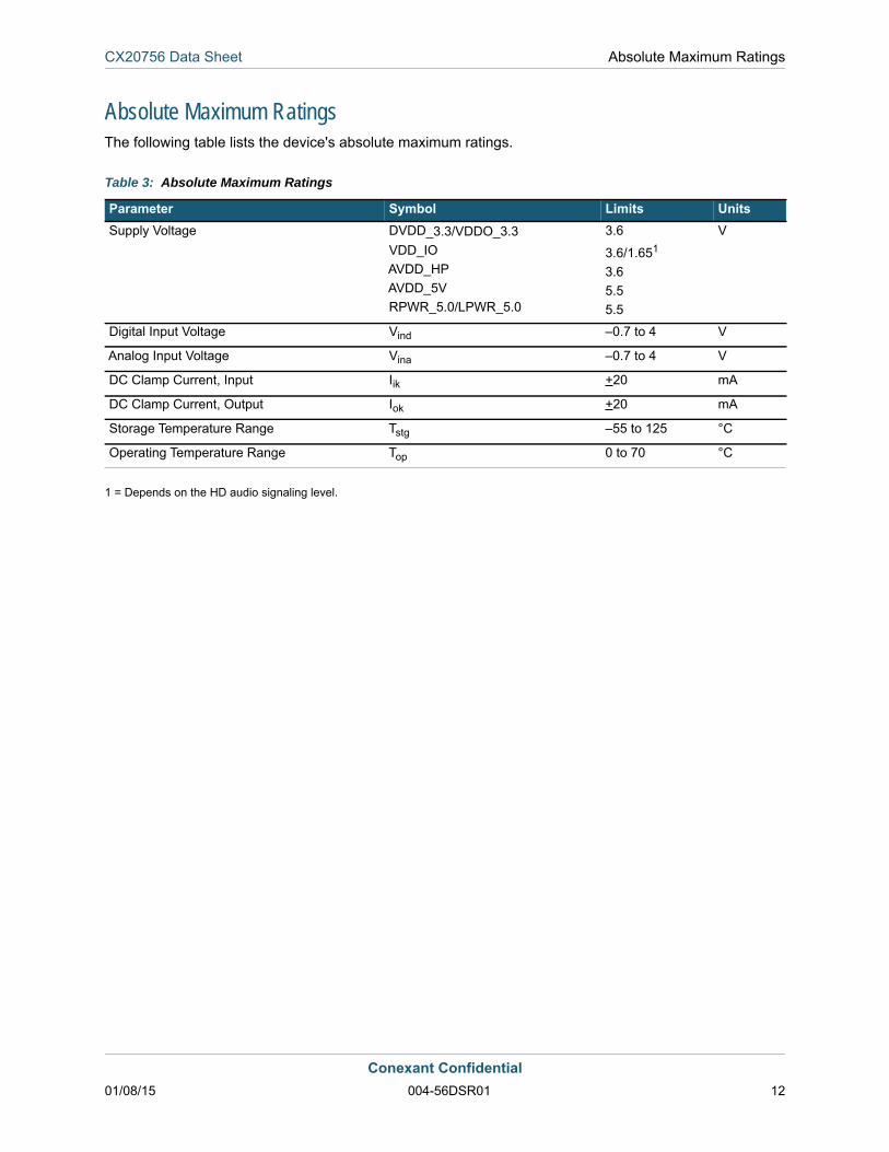
Absolute Maximum RatingsThe following table lists the device's absolute maximum ratings.
1 = Depends on the HD audio signaling level.
Table 3: Absolute Maximum Ratings
Parameter Symbol Limits UnitsSupply Voltage DVDD_3.3/VDDO_3.3
VDD_IOAVDD_HPAVDD_5VRPWR_5.0/LPWR_5.0
3.6
3.6/1.651
3.65.55.5
V
Digital Input Voltage Vind –0.7 to 4 V
Analog Input Voltage Vina –0.7 to 4 V
DC Clamp Current, Input Iik +20 mA
DC Clamp Current, Output Iok +20 mA
Storage Temperature Range Tstg –55 to 125 °C
Operating Temperature Range Top 0 to 70 °C
Conexant Confidential01/08/15 004-56DSR01 12
CX20756 Data Sheet Electrical Characteristics
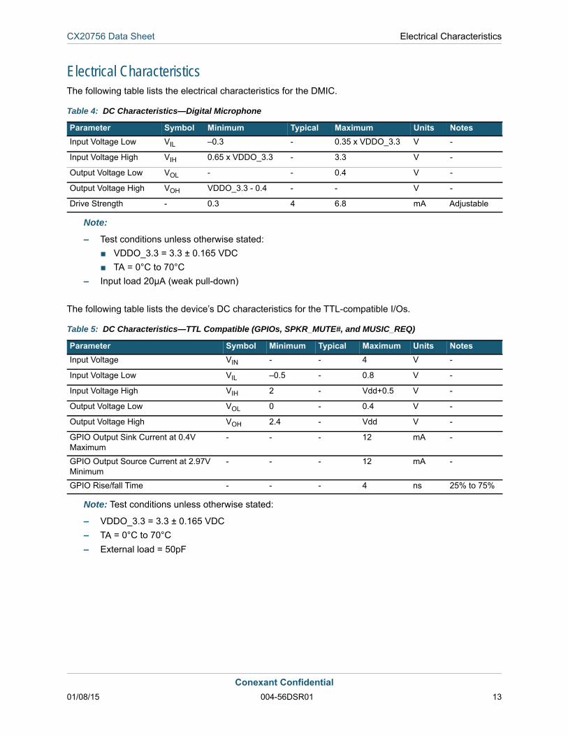
Electrical CharacteristicsThe following table lists the electrical characteristics for the DMIC.
Note:
– Test conditions unless otherwise stated: ■ VDDO_3.3 = 3.3 ± 0.165 VDC■ TA = 0°C to 70°C
– Input load 20μA (weak pull-down)
The following table lists the device’s DC characteristics for the TTL-compatible I/Os.
Note: Test conditions unless otherwise stated:
– VDDO_3.3 = 3.3 ± 0.165 VDC– TA = 0°C to 70°C– External load = 50pF
Table 4: DC Characteristics—Digital Microphone
Parameter Symbol Minimum Typical Maximum Units NotesInput Voltage Low VIL –0.3 - 0.35 x VDDO_3.3 V -
Input Voltage High VIH 0.65 x VDDO_3.3 - 3.3 V -
Output Voltage Low VOL - - 0.4 V -
Output Voltage High VOH VDDO_3.3 - 0.4 - - V -
Drive Strength - 0.3 4 6.8 mA Adjustable
Table 5: DC Characteristics—TTL Compatible (GPIOs, SPKR_MUTE#, and MUSIC_REQ)
Parameter Symbol Minimum Typical Maximum Units NotesInput Voltage VIN - - 4 V -
Input Voltage Low VIL –0.5 - 0.8 V -
Input Voltage High VIH 2 - Vdd+0.5 V -
Output Voltage Low VOL 0 - 0.4 V -
Output Voltage High VOH 2.4 - Vdd V -
GPIO Output Sink Current at 0.4V Maximum
- - - 12 mA -
GPIO Output Source Current at 2.97V Minimum
- - - 12 mA -
GPIO Rise/fall Time - - - 4 ns 25% to 75%
Conexant Confidential01/08/15 004-56DSR01 13

CX20756 Data Sheet Device Performance Specifications
Device Performance SpecificationsThe tables and graphs in this section illustrate the device’s analog performance.
Table 6: Analog Performance Characteristics
Parameter Minimum Typical Maximum UnitsHeadphone OutputFull Scale Output Voltage - 1 - VRMS
Dynamic Range (Measured with –60dBFS Signal Present) - 99 - dBFS
Total Harmonic Distortion Plus Noise (THD+N), Measured at –3dBFS - –86 - dB
Channel Crosstalk - –75 - dBFS
Analog Frequency Response (±3dB at 20Hz, ±1dB at 20000Hz) 20 - 20000 Hz
Class-D Speaker Amplifier OutputsFull Scale Output Voltage (into 4) -
-42.90
--
VpVRMS
Dynamic Range (Measured with –60dBFS Signal Present) - 94 - dBFS
THD+N, Measured at –3dBFS - –65 - dBFS
Analog Frequency Response (±3dB at 20Hz, ±1dB at 20000Hz) 20 - 20000 Hz
Efficiency (Measured at 1W/Ch) - 85 - %
Line InputsFull Scale Input Voltage 1 - - VRMS
Dynamic Range (Measured with –60dBFS Signal Present) - 92 - dBFS
THD+N, Measured at –3dBFS - –87 - dB
Channel Crosstalk - –84 - dBFS
Analog Frequency Response (±3dB at 200Hz, ±1dB at 20000Hz) 20 - 20000 Hz
Input Resistance—0dB - 15.8 - k
Input Capacitance - 5 - pF
Microphone InputsFull Scale Input Voltage with:
20dB boostBoost off
0.11
--
--
VRMS
-
Dynamic Range (Measured with –60dBFS Signal Present) - 91 - dBFS
THD+N, Measured at –3dBFS - –87 - dB
Channel Crosstalk (Measured at 1kHz, 0dB Gain) - –84 - dBFS
Analog Frequency Response (±3dB at 200Hz, ±1dB at 20000Hz) 100 - 20000 Hz
Input Resistance0dB10dB–40dB
15.85
--
k-
Input Capacitance - 5 - pF
Conexant Confidential01/08/15 004-56DSR01 14
CX20756 Data Sheet Device Performance Specifications
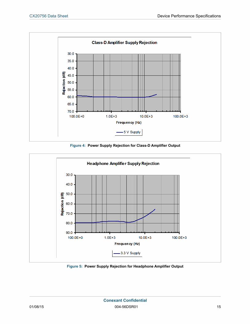
Figure 4: Power Supply Rejection for Class-D Amplifier Output
Figure 5: Power Supply Rejection for Headphone Amplifier Output
Conexant Confidential01/08/15 004-56DSR01 15
CX20756 Data Sheet Device Performance Specifications
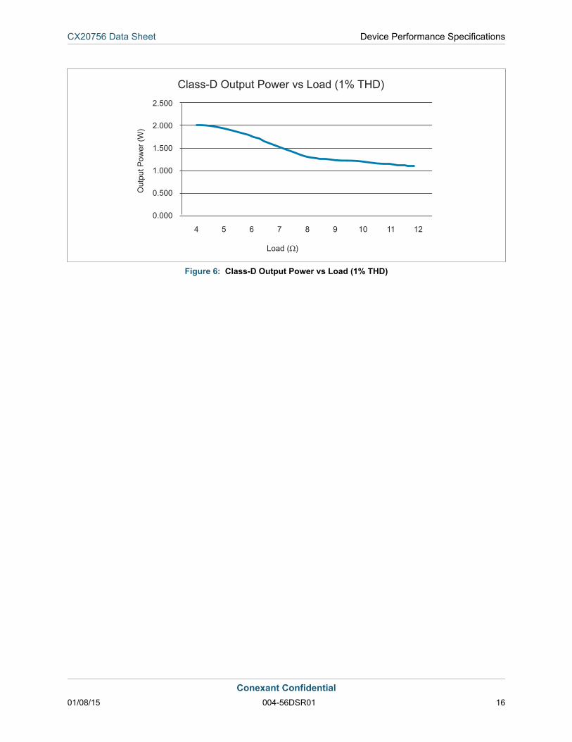
Figure 6: Class-D Output Power vs Load (1% THD)
Load (Ω)
Class-D Output Power vs Load (1% THD)2.500
2.000
1.500
1.000
0.500
0.000
4 5 6 7 8 9 10 11 12
Out
put P
ower
(W)
Conexant Confidential01/08/15 004-56DSR01 16
CX20756 Data Sheet Power Management and Power Consumption
Power Management and Power Consumption
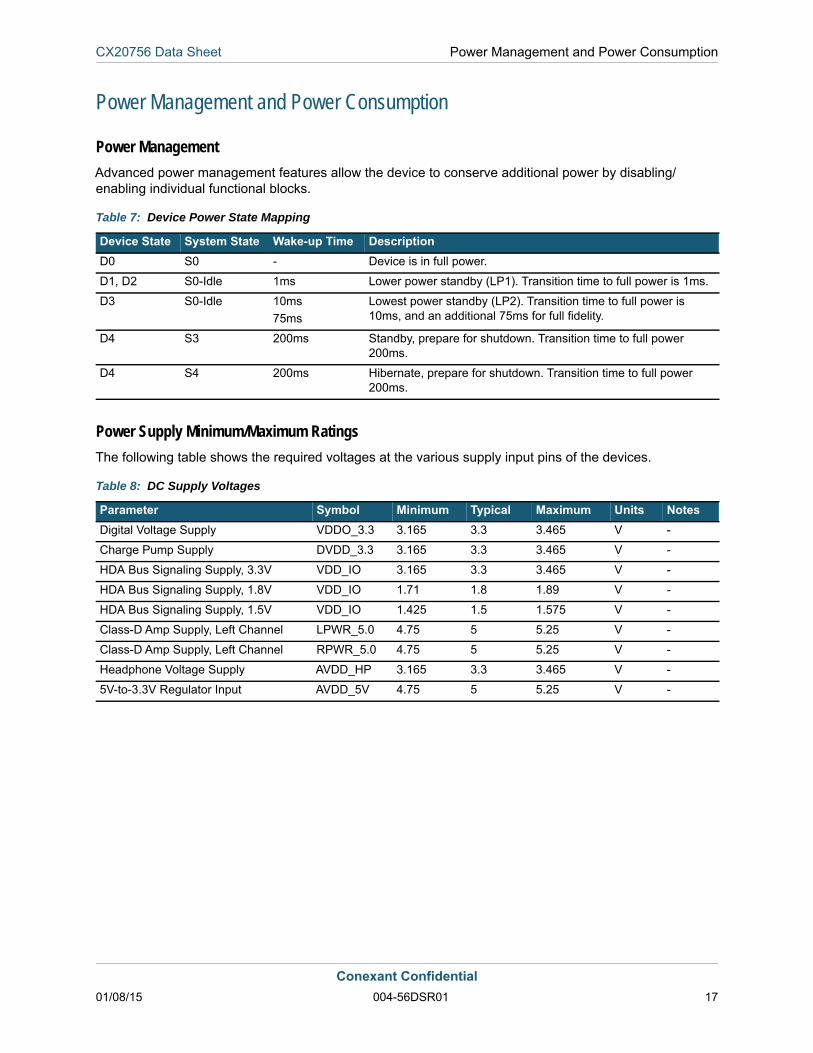
Power ManagementAdvanced power management features allow the device to conserve additional power by disabling/enabling individual functional blocks.
Power Supply Minimum/Maximum RatingsThe following table shows the required voltages at the various supply input pins of the devices.
Table 7: Device Power State Mapping
Device State System State Wake-up Time DescriptionD0 S0 - Device is in full power.
D1, D2 S0-Idle 1ms Lower power standby (LP1). Transition time to full power is 1ms.
D3 S0-Idle 10ms75ms
Lowest power standby (LP2). Transition time to full power is 10ms, and an additional 75ms for full fidelity.
D4 S3 200ms Standby, prepare for shutdown. Transition time to full power 200ms.
D4 S4 200ms Hibernate, prepare for shutdown. Transition time to full power 200ms.
Table 8: DC Supply Voltages
Parameter Symbol Minimum Typical Maximum Units NotesDigital Voltage Supply VDDO_3.3 3.165 3.3 3.465 V -
Charge Pump Supply DVDD_3.3 3.165 3.3 3.465 V -
HDA Bus Signaling Supply, 3.3V VDD_IO 3.165 3.3 3.465 V -
HDA Bus Signaling Supply, 1.8V VDD_IO 1.71 1.8 1.89 V -
HDA Bus Signaling Supply, 1.5V VDD_IO 1.425 1.5 1.575 V -
Class-D Amp Supply, Left Channel LPWR_5.0 4.75 5 5.25 V -
Class-D Amp Supply, Left Channel RPWR_5.0 4.75 5 5.25 V -
Headphone Voltage Supply AVDD_HP 3.165 3.3 3.465 V -
5V-to-3.3V Regulator Input AVDD_5V 4.75 5 5.25 V -
Conexant Confidential01/08/15 004-56DSR01 17
CX20756 Data Sheet Power Management and Power Consumption
Power Consumption
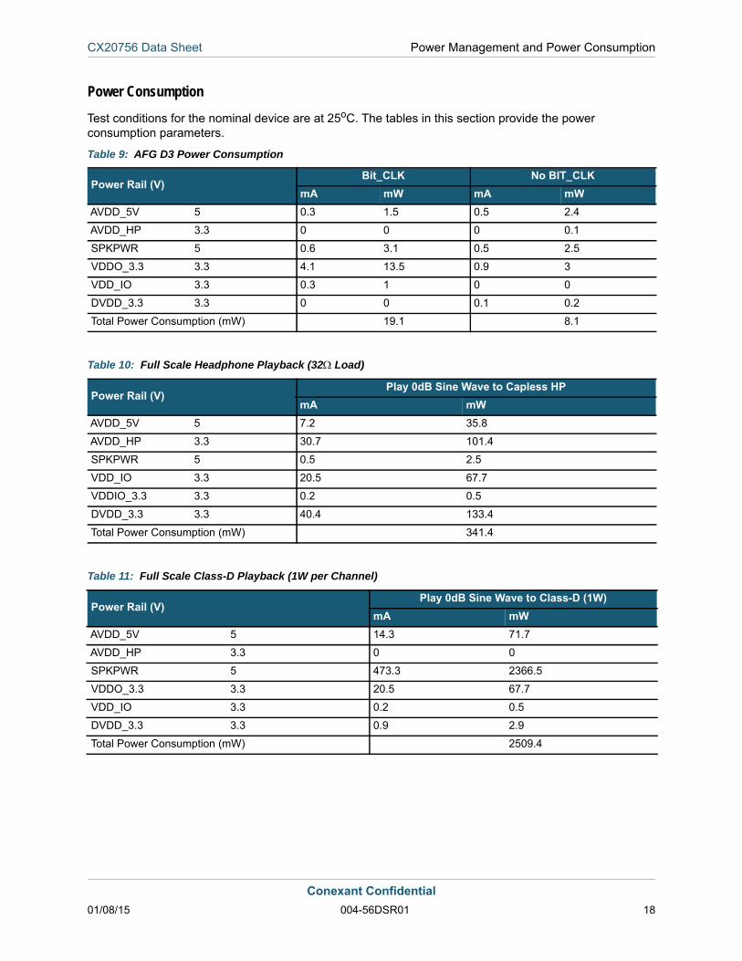
Test conditions for the nominal device are at 25oC. The tables in this section provide the power consumption parameters.
Table 9: AFG D3 Power Consumption
Power Rail (V)Bit_CLK No BIT_CLK
mA mW mA mWAVDD_5V 5 0.3 1.5 0.5 2.4
AVDD_HP 3.3 0 0 0 0.1
SPKPWR 5 0.6 3.1 0.5 2.5
VDDO_3.3 3.3 4.1 13.5 0.9 3
VDD_IO 3.3 0.3 1 0 0
DVDD_3.3 3.3 0 0 0.1 0.2
Total Power Consumption (mW) 19.1 8.1
Table 10: Full Scale Headphone Playback (32 Load)
Power Rail (V)Play 0dB Sine Wave to Capless HP
mA mWAVDD_5V 5 7.2 35.8
AVDD_HP 3.3 30.7 101.4
SPKPWR 5 0.5 2.5
VDD_IO 3.3 20.5 67.7
VDDIO_3.3 3.3 0.2 0.5
DVDD_3.3 3.3 40.4 133.4
Total Power Consumption (mW) 341.4
Table 11: Full Scale Class-D Playback (1W per Channel)
Power Rail (V)Play 0dB Sine Wave to Class-D (1W)
mA mWAVDD_5V 5 14.3 71.7
AVDD_HP 3.3 0 0
SPKPWR 5 473.3 2366.5
VDDO_3.3 3.3 20.5 67.7
VDD_IO 3.3 0.2 0.5
DVDD_3.3 3.3 0.9 2.9
Total Power Consumption (mW) 2509.4
Conexant Confidential01/08/15 004-56DSR01 18

CX20756 Data Sheet Power Management and Power Consumption
Integrated Low Drop-Out (LDO) RegulatorsThe devices feature the following two integrated LDO voltage regulators:
• 5V to 3.3V regulator = Although the output of this voltage regulator (AVDD_3.3) can be used to power external circuitry (e.g., low-power analog), external current consumption from the regulator should be limited to no more than 30mA. Additionally, caution should be used when powering external circuitry, and use filtering (e.g., ferrite bead plus capacitor) to prevent the external circuitry from adding noise to the AVDD_3.3 voltage rail.
• 3.3V to 1.8V regulator = The output of this voltage regulator (FILT_1.8) can also be used to power external circuitry (e.g., discrete logic).
Table 12: Line-In Recording
Power Rail (V)Line-In Record from Port B
mA mWAVDD_5V 5 8.8 43.9
AVDD_HP 3.3 0 0
SPKPWR 5 0.5 2.5
VDDO_3.3 3.3 18.9 62.4
VDD_IO 3.3 0.4 1.2
DVDD_3.3 3.3 0.1 0.2
Total Power Consumption (mW) 110.2
Conexant Confidential01/08/15 004-56DSR01 19
CX20756 Data Sheet Power Management and Power Consumption
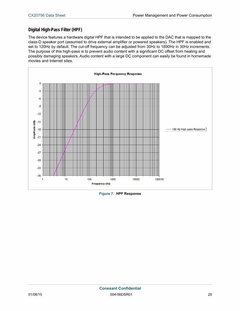
Digital High-Pass Filter (HPF)The device features a hardware digital HPF that is intended to be applied to the DAC that is mapped to the class-D speaker port (assumed to drive external amplifier or powered speakers). The HPF is enabled and set to 120Hz by default. The cut-off frequency can be adjusted from 30Hz to 1890Hz in 30Hz increments. The purpose of this high-pass is to prevent audio content with a significant DC offset from heating and possibly damaging speakers. Audio content with a large DC component can easily be found in homemade movies and Internet sites.
Figure 7: HPF Response
Conexant Confidential01/08/15 004-56DSR01 20
CX20756 Data Sheet Alternating Current (AC) Timing Characteristics
Alternating Current (AC) Timing Characteristics
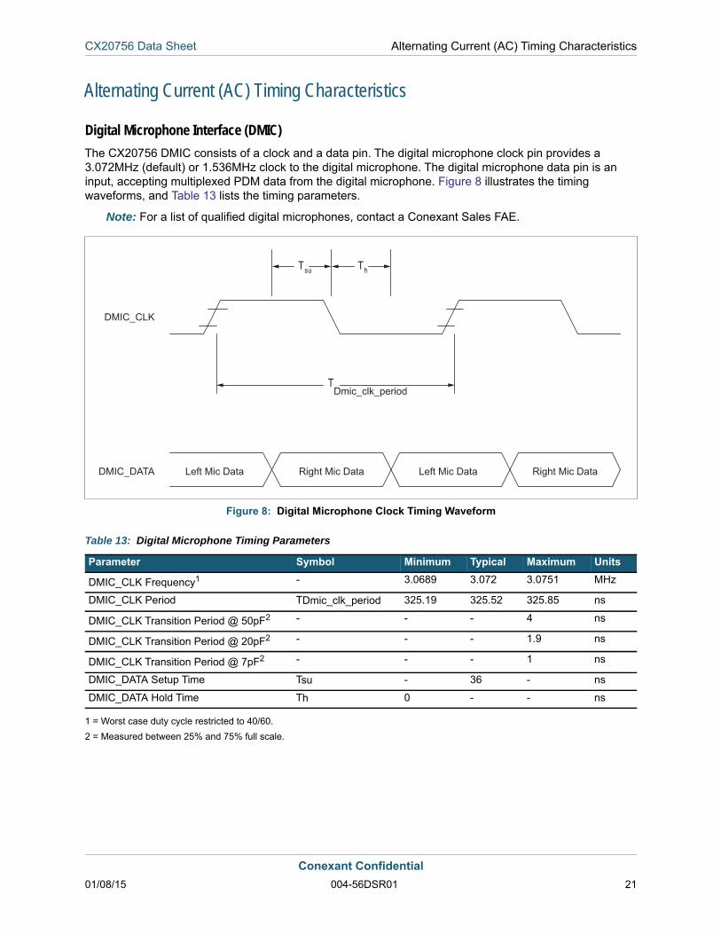
Digital Microphone Interface (DMIC)The CX20756 DMIC consists of a clock and a data pin. The digital microphone clock pin provides a 3.072MHz (default) or 1.536MHz clock to the digital microphone. The digital microphone data pin is an input, accepting multiplexed PDM data from the digital microphone. Figure 8 illustrates the timing waveforms, and Table 13 lists the timing parameters.
Note: For a list of qualified digital microphones, contact a Conexant Sales FAE.
Figure 8: Digital Microphone Clock Timing Waveform
1 = Worst case duty cycle restricted to 40/60.2 = Measured between 25% and 75% full scale.
Table 13: Digital Microphone Timing Parameters
Parameter Symbol Minimum Typical Maximum Units
DMIC_CLK Frequency1 - 3.0689 3.072 3.0751 MHz
DMIC_CLK Period TDmic_clk_period 325.19 325.52 325.85 ns
DMIC_CLK Transition Period @ 50pF2 - - - 4 ns
DMIC_CLK Transition Period @ 20pF2 - - - 1.9 ns
DMIC_CLK Transition Period @ 7pF2 - - - 1 ns
DMIC_DATA Setup Time Tsu - 36 - ns
DMIC_DATA Hold Time Th 0 - - ns
T
T Tsu h
DMIC_CLK
DMIC_DATA
Dmic_clk_period
Left Mic Data Right Mic Data Left Mic Data Right Mic Data
Conexant Confidential01/08/15 004-56DSR01 21

CX20756 Data Sheet Alternating Current (AC) Timing Characteristics
HD Audio ClocksThe BIT_CLK signal is a 24MHz clock that is sourced from the HD audio controller and connected to all CODECs on the link. Figure 9 and Table 14 show the HD audio clock waveforms and timing parameters.
Figure 9: BIT_CLK and SYNC Timing Waveforms
1 = 47.5pF–70pF external load.2 = Worst-case duty cycle restricted to 40/60.3 = The SYNC frequency is equal to the BIT_CLK frequency, divided by 500.
Table 14: BIT_CLK and SYNC Timing Parameters
Parameter Symbol Minimum Typical Maximum UnitsBIT_CLK Frequency - 23.9976 24 24.0024 MHz
BIT_CLK Period Tclk_period 41.363 41.67 41.971 ns
BIT_CLK Output Jitter - - 150 500 Ps
BIT_CLK High Pulse Width1,2 Tclk_high 18.75 - 22.91 ns
BIT_CLK Low Pulse Width1,2 Tclk_low 18.75 - 22.91 ns
SYNC Frequency3 - - 48 - kHz
SYNC Period Tsync_period - 20.8 - μs
SYNC High Pulse Width Tsync_high - 4 x Tclk_period - μs
T
T
T
TT
clk_period
sync_period
clk_low
clk_high
sync_high
BIT_CLK
SYNC
Conexant Confidential01/08/15 004-56DSR01 22
CX20756 Data Sheet Alternating Current (AC) Timing Characteristics
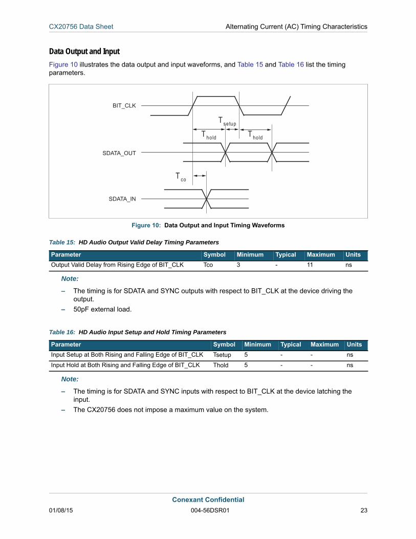
Data Output and InputFigure 10 illustrates the data output and input waveforms, and Table 15 and Table 16 list the timing parameters.
Figure 10: Data Output and Input Timing Waveforms
Note:
– The timing is for SDATA and SYNC outputs with respect to BIT_CLK at the device driving the output.
– 50pF external load.
Note:
– The timing is for SDATA and SYNC inputs with respect to BIT_CLK at the device latching the input.
– The CX20756 does not impose a maximum value on the system.
Table 15: HD Audio Output Valid Delay Timing Parameters
Parameter Symbol Minimum Typical Maximum UnitsOutput Valid Delay from Rising Edge of BIT_CLK Tco 3 - 11 ns
Table 16: HD Audio Input Setup and Hold Timing Parameters
Parameter Symbol Minimum Typical Maximum UnitsInput Setup at Both Rising and Falling Edge of BIT_CLK Tsetup 5 - - ns
Input Hold at Both Rising and Falling Edge of BIT_CLK Thold 5 - - ns
T hold T hold
T setup
T co
BIT_CLK
SDATA_OUT
SDATA_IN
Conexant Confidential01/08/15 004-56DSR01 23
CX20756 Data Sheet Package Dimensions and Thermal Specifications
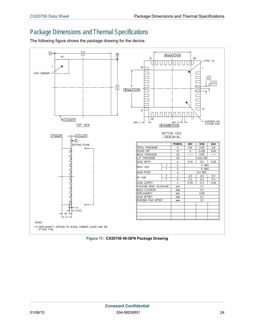
Package Dimensions and Thermal SpecificationsThe following figure shows the package drawing for the device.
Figure 11: CX20756 40-QFN Package Drawing
Conexant Confidential01/08/15 004-56DSR01 24
CX20756 Data Sheet Package Dimensions and Thermal Specifications
The following table defines the thermal specifications.
Note: Measurements per JEDEC EIA/JESD 51. The JA of application boards with more than four layers stay the same or improve if the PCB construction is similar to the JEDEC EIA/JESD 51 defined four-layer PCB (2S2P plus vias).
Table 17: Thermal Specifications
Parameter Symbol Minimum Typical Maximum Units NotesTheta-JA (Junction-to-Ambient Thermal Resistance)
JA - 36.2 - oC/W Four-layer PCB with solid ground plane and thermal vias (still air).
Psi-JT (Junction-to-Package Top Thermal Characterization Parameter)
JT - 0.39 - oC/W Four-layer PCB with solid ground plane and thermal vias (still air).
Conexant Confidential01/08/15 004-56DSR01 25
CX20756 Data Sheet HD Audio Interface
HD Audio Interface
OverviewThe HD audio interface is a five-pin interface:
• Clock (BIT_CLK)• Serial data in (SDATA_IN)• Serial data out (SDATA_OUT)• SYNC• RESET#
The clock is provided by the controller at a frequency of 24MHz. Because the SDATA_OUT signal is provided by the controller and contains data for every edge of the 24MHz clock, the CX20756 must sample data on both rising and falling edges of SDATA_OUT.
The SYNC signal not only signals the beginning of the 500 clock frame, it designates the beginning of the data for each stream and indicates which stream of data is to be on SDATA_OUT next (streams do not need to appear in order; the controller may do as it likes). Channels are another way of organizing the serial data. Each stream has at least one channel. Each stream must start with channel 0 and proceed without interruption until all the assigned channels are exhausted. A stereo pair takes two adjacent channels.
The SDATA_IN signal contains the CX20756 data headed towards the controller, and is only generated on rising edges. This includes information read from the HD audio registers, ADC, and incoming modem data. The stream and channel are indicated before the data is transmitted on SDATA_IN (refer to Intel’s HD Audio Specification 1.0a for the format). The SDATA_IN signal is responsible for knowing the device number, which is the CODEC Address (CAd) in Intel’s HD Audio Specification 1.0a. During the last clock of the first sync after a Power-on Reset (PoR), the SDATA_IN is driven high by the CX20756 for one clock cycle. This indicates to the controller the need for a CAd. The CX20756 then stops driving the SDATA_IN signal, and the controller begins to drive it. The controller drives SDATA_IN high through the next sync, and the CAd is assigned by the number of clocks after the fall of sync that it takes for the SDATA_IN to fall. The interface then turns around again, and SDATA_IN is an output from the CX20756 until reset.
Intel’s HD Audio Specification 1.0a also contains one other concept of an unsolicited message. Unsolicited messages can occur for a number of reasons, such as timers, ringing phones, answers from the device to a register read, etc. Because the bus has no interrupt, these reasons are taken care of in unsolicited messages. If the controller was not addressing the CAd assigned to the CX20756 during the previous frame and if one of these unsolicited messages is needed (and enabled), the CX20756 uses the first cycles after the sync on SDATA_IN to alert the controller to the event. Only one event can be signaled in a frame.
The CX20756 only sends the message once, and does not expect any sort of acknowledgment from the controller.
Conexant Confidential01/08/15 004-56DSR01 26
CX20756 Data Sheet Verbs
VerbsThis section describes how this device interacts with the verbs defined in Intel’s HD Audio Specification 1.0a. Each of the following subsections describe the verb IDs, parameters/payload, and corresponding responses that apply to that node.
Verbs are commands and queries that are passed from the HD audio controller to the CODECs on the HD audio bus. Responses are data passed from the HD audio CODEC to the HD audio controller. All controller verbs must be followed by a CODEC response. Unsolicited responses from the CODEC are data transmitted without a controller verb request.
A 1 in the:
• Valid bit position indicates the Response field contains a valid response. • UnSol bit position is meaningful only when the Valid bit is set, and indicates that the response is
unsolicited rather than in reply to a verb.
The 32 actual response bits vary in format and are each documented in Intel’s HD Audio Specification 1.0a.
Note: For more information regarding the verbs, controller, CODEC commands, and control protocol, refer to Intel’s HD Audio Specification 1.0a document.
Each node in the CODEC is addressed using a CAd that is assigned to the CODEC during initialization, and the Node's ID (NID). The concatenation of the CAd and NID provide a unique address that allows commands to reference a specific node within the audio subsystem.
The entire verb is formed by pre-pending the CAd and the NID to the verb ID and parameter/payload. In this section’s tables and descriptions, the CAd and NID are not listed as part of the verb.
Register values may have up to five letters included with their default value. These letters indicate which of the possible reset events force the register to its default value. The five letters are as follows:
• P = Power-on reset• R = HD audio reset pin assertion• V = Single verb reset• W = Double verb reset• D = D-state change reset
Only the letters in the list force the register to its default value.
Conexant Confidential01/08/15 004-56DSR01 27
CX20756 Data Sheet Verbs
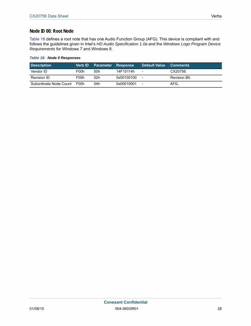
Node ID 00: Root NodeTable 18 defines a root note that has one Audio Function Group (AFG). This device is compliant with and follows the guidelines given in Intel’s HD Audio Specification 1.0a and the Windows Logo Program Device Requirements for Windows 7 and Windows 8.
Table 18: Node 0 Responses
Description Verb ID Parameter Response Default Value CommentsVendor ID F00h 00h 14F15114h - CX20756.
Revision ID F00h 02h 0x00100100 - Revision B0.
Subordinate Node Count F00h 04h 0x00010001 - AFG.
Conexant Confidential01/08/15 004-56DSR01 28
CX20756 Data Sheet Verbs
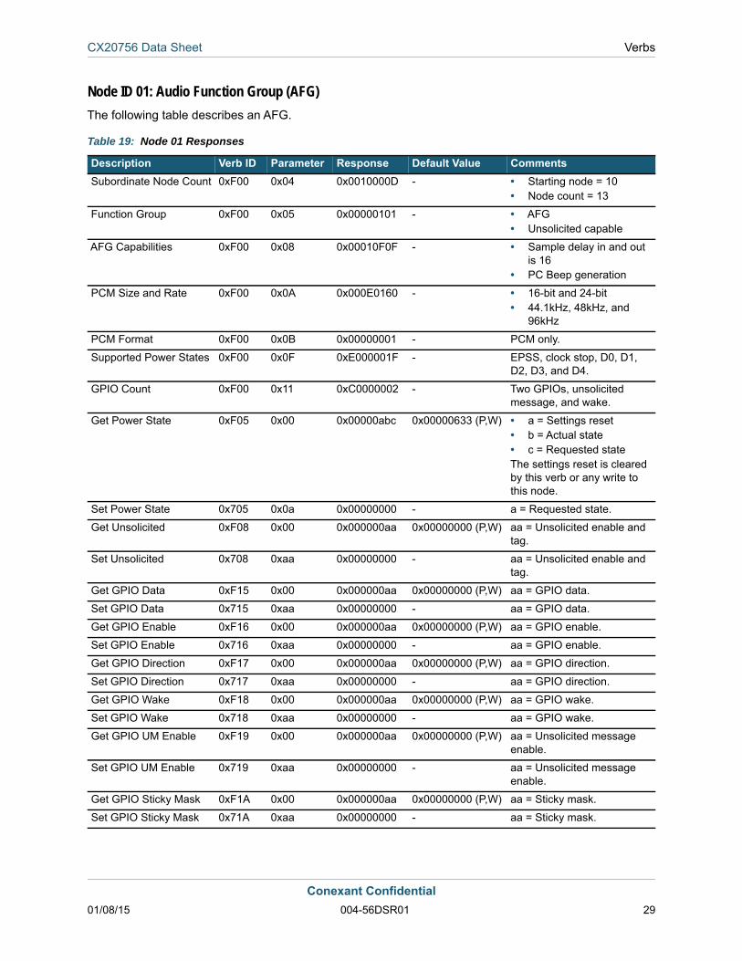
Node ID 01: Audio Function Group (AFG)The following table describes an AFG.
Table 19: Node 01 Responses
Description Verb ID Parameter Response Default Value CommentsSubordinate Node Count 0xF00 0x04 0x0010000D - • Starting node = 10
• Node count = 13
Function Group 0xF00 0x05 0x00000101 - • AFG• Unsolicited capable
AFG Capabilities 0xF00 0x08 0x00010F0F - • Sample delay in and out is 16
• PC Beep generation
PCM Size and Rate 0xF00 0x0A 0x000E0160 - • 16-bit and 24-bit• 44.1kHz, 48kHz, and
96kHz
PCM Format 0xF00 0x0B 0x00000001 - PCM only.
Supported Power States 0xF00 0x0F 0xE000001F - EPSS, clock stop, D0, D1, D2, D3, and D4.
GPIO Count 0xF00 0x11 0xC0000002 - Two GPIOs, unsolicited message, and wake.
Get Power State 0xF05 0x00 0x00000abc 0x00000633 (P,W) • a = Settings reset• b = Actual state• c = Requested stateThe settings reset is cleared by this verb or any write to this node.
Set Power State 0x705 0x0a 0x00000000 - a = Requested state.
Get Unsolicited 0xF08 0x00 0x000000aa 0x00000000 (P,W) aa = Unsolicited enable and tag.
Set Unsolicited 0x708 0xaa 0x00000000 - aa = Unsolicited enable and tag.
Get GPIO Data 0xF15 0x00 0x000000aa 0x00000000 (P,W) aa = GPIO data.
Set GPIO Data 0x715 0xaa 0x00000000 - aa = GPIO data.
Get GPIO Enable 0xF16 0x00 0x000000aa 0x00000000 (P,W) aa = GPIO enable.
Set GPIO Enable 0x716 0xaa 0x00000000 - aa = GPIO enable.
Get GPIO Direction 0xF17 0x00 0x000000aa 0x00000000 (P,W) aa = GPIO direction.
Set GPIO Direction 0x717 0xaa 0x00000000 - aa = GPIO direction.
Get GPIO Wake 0xF18 0x00 0x000000aa 0x00000000 (P,W) aa = GPIO wake.
Set GPIO Wake 0x718 0xaa 0x00000000 - aa = GPIO wake.
Get GPIO UM Enable 0xF19 0x00 0x000000aa 0x00000000 (P,W) aa = Unsolicited message enable.
Set GPIO UM Enable 0x719 0xaa 0x00000000 - aa = Unsolicited message enable.
Get GPIO Sticky Mask 0xF1A 0x00 0x000000aa 0x00000000 (P,W) aa = Sticky mask.
Set GPIO Sticky Mask 0x71A 0xaa 0x00000000 - aa = Sticky mask.
Conexant Confidential01/08/15 004-56DSR01 29
CX20756 Data Sheet Verbs
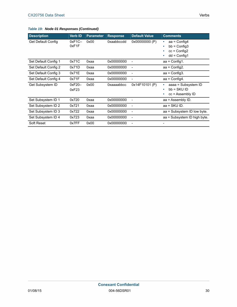
Get Default Config 0xF1C–0xF1F
0x00 0xaabbccdd 0x00000000 (P) • aa = Config4• bb = Config3• cc = Config2• dd = Config1
Set Default Config 1 0x71C 0xaa 0x00000000 - aa = Config1.
Set Default Config 2 0x71D 0xaa 0x00000000 - aa = Config2.
Set Default Config 3 0x71E 0xaa 0x00000000 - aa = Config3.
Set Default Config 4 0x71F 0xaa 0x00000000 - aa = Config4.
Get Subsystem ID 0xF20–0xF23
0x00 0xaaaabbcc 0x14F10101 (P) • aaaa = Subsystem ID• bb = SKU ID• cc = Assembly ID
Set Subsystem ID 1 0x720 0xaa 0x00000000 - aa = Assembly ID.
Set Subsystem ID 2 0x721 0xaa 0x00000000 - aa = SKU ID.
Set Subsystem ID 3 0x722 0xaa 0x00000000 - aa = Subsystem ID low byte.
Set Subsystem ID 4 0x723 0xaa 0x00000000 - aa = Subsystem ID high byte.
Soft Reset 0x7FF 0x00 0x00000000 - -
Table 19: Node 01 Responses (Continued)
Description Verb ID Parameter Response Default Value Comments
Conexant Confidential01/08/15 004-56DSR01 30
CX20756 Data Sheet Verbs
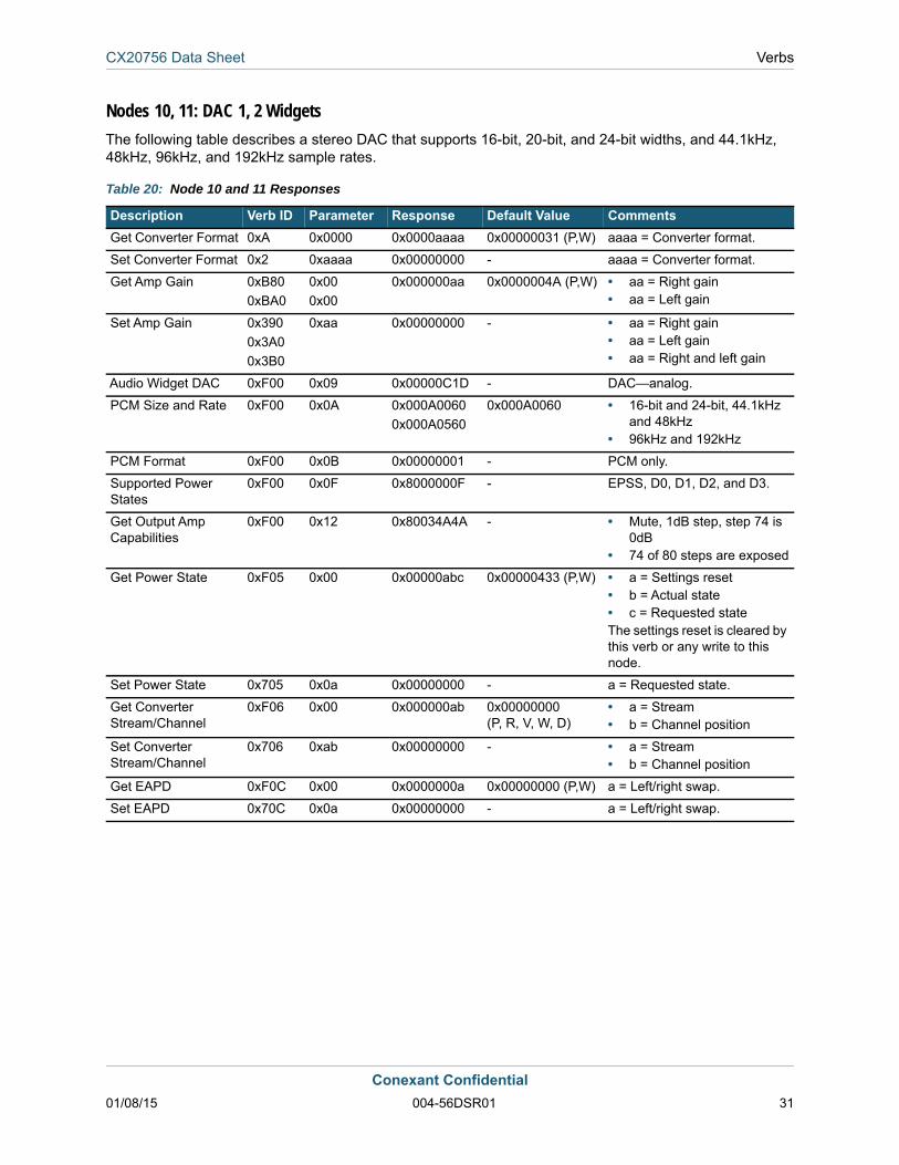
Nodes 10, 11: DAC 1, 2 WidgetsThe following table describes a stereo DAC that supports 16-bit, 20-bit, and 24-bit widths, and 44.1kHz, 48kHz, 96kHz, and 192kHz sample rates.
Table 20: Node 10 and 11 Responses
Description Verb ID Parameter Response Default Value CommentsGet Converter Format 0xA 0x0000 0x0000aaaa 0x00000031 (P,W) aaaa = Converter format.
Set Converter Format 0x2 0xaaaa 0x00000000 - aaaa = Converter format.
Get Amp Gain 0xB800xBA0
0x000x00
0x000000aa 0x0000004A (P,W) • aa = Right gain• aa = Left gain
Set Amp Gain 0x3900x3A00x3B0
0xaa 0x00000000 - • aa = Right gain• aa = Left gain• aa = Right and left gain
Audio Widget DAC 0xF00 0x09 0x00000C1D - DAC—analog.
PCM Size and Rate 0xF00 0x0A 0x000A00600x000A0560
0x000A0060 • 16-bit and 24-bit, 44.1kHz and 48kHz
• 96kHz and 192kHz
PCM Format 0xF00 0x0B 0x00000001 - PCM only.
Supported Power States
0xF00 0x0F 0x8000000F - EPSS, D0, D1, D2, and D3.
Get Output Amp Capabilities
0xF00 0x12 0x80034A4A - • Mute, 1dB step, step 74 is 0dB
• 74 of 80 steps are exposed
Get Power State 0xF05 0x00 0x00000abc 0x00000433 (P,W) • a = Settings reset• b = Actual state• c = Requested stateThe settings reset is cleared by this verb or any write to this node.
Set Power State 0x705 0x0a 0x00000000 - a = Requested state.
Get Converter Stream/Channel
0xF06 0x00 0x000000ab 0x00000000 (P, R, V, W, D)
• a = Stream• b = Channel position
Set Converter Stream/Channel
0x706 0xab 0x00000000 - • a = Stream• b = Channel position
Get EAPD 0xF0C 0x00 0x0000000a 0x00000000 (P,W) a = Left/right swap.
Set EAPD 0x70C 0x0a 0x00000000 - a = Left/right swap.
Conexant Confidential01/08/15 004-56DSR01 31

CX20756 Data Sheet Verbs
Node 12: PC Beep Generator WidgetTable 21 describes a beep generator. PC beep is mixed in with all enabled output ports while in D0. When the PC beep input pin is connected but inactive, while not toggling no system noise is injected on the output pins. If the PC beep input is left unconnected, there is no impact on the performance of the output ports.
This is a mono widget. Only the left channel volume request is valid. Any request, read, or write with the right channel is ignored and returns 0x00000000. If both left and right are present in the request, only the value from the left side is used.
The beep gain level range (–4dB to –32dB) is for the speaker port. The default setting is –28dB on the speaker, and –46dB on the headphone.
Table 21: PC Beep Generator Responses
Description Verb ID Parameter Response Default Value CommentsGet Amp Gain 0xBA0 0x00 0x0000000a 0x00000001 (P,W) aa = Left gain.
Set Amp Gain 0x3A00x3B0
0xaa 0x00000000 - • aa = Left gain• aa = Left gain
Audio Widget PC Beep 0xF00 0x09 0x0070000C - PC Beep generator with an output amp.
Get Output Amp Capabilities
0xF00 0x12 0x000F0707 - 4dB step, eight steps, and step 8 is –4dB.
Get Beep Generation Control
0xF0A 0x00 0x000000aa 0x00000000 (P,W) aa = Divider.
Set Beep Generation Control
0x70A 0xaa 0x00000000 - aa = Divider.
Conexant Confidential01/08/15 004-56DSR01 32
CX20756 Data Sheet Verbs
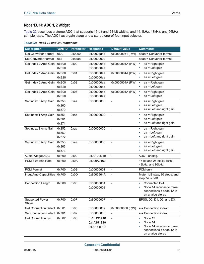
Node 13, 14: ADC 1, 2 WidgetTable 22 describes a stereo ADC that supports 16-bit and 24-bit widths, and 44.1kHz, 48kHz, and 96kHz sample rates. The ADC has a gain stage and a stereo one-of-four input selector.
Table 22: Node 13 and 14 Responses
Description Verb ID Parameter Response Default Value CommentsGet Converter Format 0xA 0x0000 0x0000aaaa 0x00000031 (P,W) aaaa = Converter format.
Set Converter Format 0x2 0xaaaa 0x00000000 - aaaa = Converter format.
Get Index 0 Amp Gain 0xB000xB20
0x00 0x000000aa0x000000aa
0x0000004A (P,W) • aa = Right gain• aa = Left gain
Get Index 1 Amp Gain 0xB000xB20
0x01 0x000000aa0x000000aa
0x0000004A (P,W) • aa = Right gain• aa = Left gain
Get Index 2 Amp Gain 0xB000xB20
0x02 0x000000aa0x000000aa
0x0000004A (P,W) • aa = Right gain• aa = Left gain
Get Index 3 Amp Gain 0xB000xB20
0x03 0x000000aa0x000000aa
0x0000004A (P,W) • aa = Right gain• aa = Left gain
Set Index 0 Amp Gain 0x3500x3600x370
0xaa 0x00000000 - • aa = Right gain• aa = Left gain• aa = Left and right gain
Set Index 1 Amp Gain 0x3510x3610x371
0xaa 0x00000000 - • aa = Right gain• aa = Left gain• aa = Left and right gain
Set Index 2 Amp Gain 0x3520x3620x372
0xaa 0x00000000 - • aa = Right gain• aa = Left gain• aa = Left and right gain
Set Index 3 Amp Gain 0x3530x3630x373
0xaa 0x00000000 - • aa = Right gain• aa = Left gain• aa = Left and right gain
Audio Widget ADC 0xF00 0x09 0x00100D1B - ADC—analog.
PCM Size And Rate 0xF00 0x0A 0x000A0160 - 16-bit and 24-bit/44.1kHz, 48kHz, and 96kHz.
PCM Format 0xF00 0x0B 0x00000001 - PCM only.
Input Amp Capabilities 0xF00 0x0D 0x8003504A - Mute, 1dB step, 80 steps, and step 74 is 0dB.
Connection Length 0xF00 0x0E 0x000000040x00000003
- • Connected to 4• Node 14 reduces to three
connections if node 1A is an analog stereo
Supported Power States
0xF00 0x0F 0x8000000F - EPSS, D0, D1, D2, and D3.
Get Connection Select 0xF01 0x00 0x0000000a 0x00000000 (P,W) a = Connection index.
Set Connection Select 0x701 0x0a 0x00000000 - a = Connection index.
Get Connection List 0xF02 0x00 0x1E191A180x1A151E190x00151E19
- • Node 13• Node 14• Node 14 reduces to three
connections if node 1A is an analog stereo
Conexant Confidential01/08/15 004-56DSR01 33
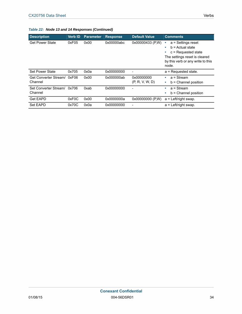
CX20756 Data Sheet Verbs
Get Power State 0xF05 0x00 0x00000abc 0x00000433 (P,W) • a = Settings reset• b = Actual state• c = Requested stateThe settings reset is cleared by this verb or any write to this node.
Set Power State 0x705 0x0a 0x00000000 - a = Requested state.
Get Converter Stream/Channel
0xF06 0x00 0x000000ab 0x00000000(P, R, V, W, D)
• a = Stream• b = Channel position
Set Converter Stream/Channel
0x706 0xab 0x00000000 - • a = Stream• b = Channel position
Get EAPD 0xF0C 0x00 0x0000000a 0x00000000 (P,W) a = Left/right swap.
Set EAPD 0x70C 0x0a 0x00000000 - a = Left/right swap.
Table 22: Node 13 and 14 Responses (Continued)
Description Verb ID Parameter Response Default Value Comments
Conexant Confidential01/08/15 004-56DSR01 34

CX20756 Data Sheet Verbs
Node 15: Mixer Widget
Table 23: Node 15 Responses
Description Verb ID Parameter Response Default Value CommentsGet Index 0 Amp Gain 0xB00
0xB200x00 0x000000aa
0x000000aa0x00000000 (P,W) • a = Right gain
• a = Left gain
Get Index 1 Amp Gain 0xB000xB20
0x01 0x000000aa0x000000aa
0x00000000 (P,W) • a = Right gain• a = Left gain
Set Index 0 Amp Gain 0x3500x3600x370
0xaa 0x00000000 - • a = Right gain• a = Left gain• a = Left and right gain
Set Index 1 Amp Gain 0x3510x3610x371
0xaa 0x00000000 - • a = Right gain• a = Left gain• a = Left and right gain
Audio Widget Mixer 0xF00 0x09 0x0020050B - Mixer with an input amplifier.
Input Amp Capabilities 0xF00 0x0D 0x80034A4A - Mute, 1dB step, 74 steps, and step 74 is 0dB.
Connection Length 0xF00 0x0E 0x00000002 - Connected to 2.
Supported Power States 0xF00 0x0F 0x8000000F - EPSS, D0, D1, D2, and D3.
Get Connection List 0xF02 0x00 0x00001110 - Connected to DAC 1, DAC 2.
Get Power State 0xF05 0x00 0x00000abc 0x00000433 (P,W) • a = Settings reset• b = Actual state• c = Requested stateThe settings reset is cleared by this verb or any write to this node.
Set Power State 0x705 0x0a 0x00000000 - a = Requested state.
Conexant Confidential01/08/15 004-56DSR01 35
CX20756 Data Sheet Verbs
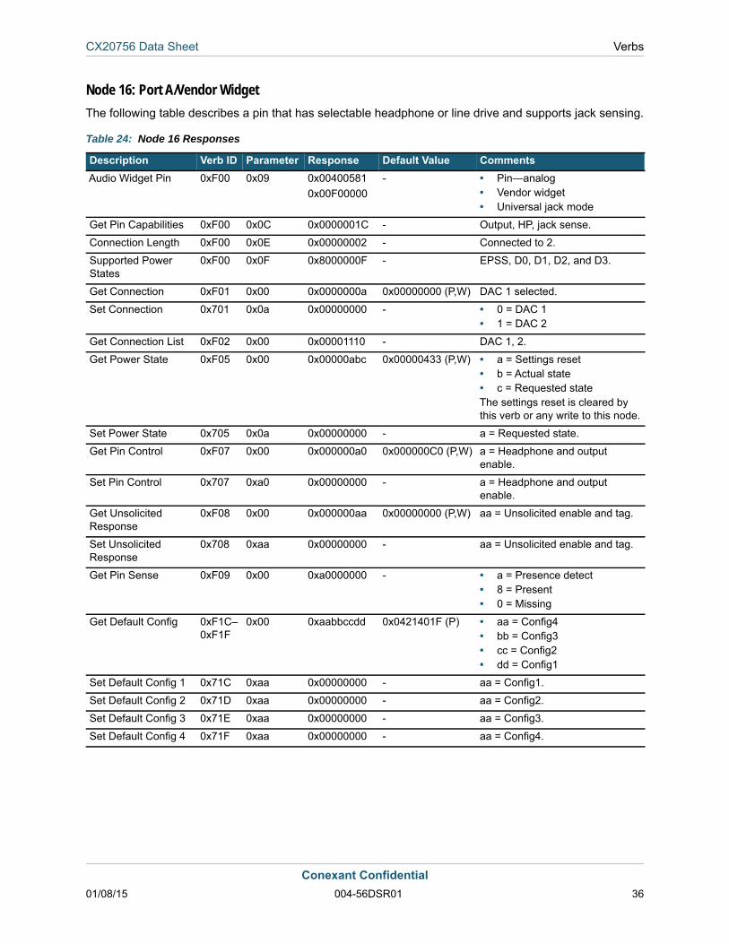
Node 16: Port A/Vendor WidgetThe following table describes a pin that has selectable headphone or line drive and supports jack sensing.
Table 24: Node 16 Responses
Description Verb ID Parameter Response Default Value CommentsAudio Widget Pin 0xF00 0x09 0x00400581
0x00F00000- • Pin—analog
• Vendor widget • Universal jack mode
Get Pin Capabilities 0xF00 0x0C 0x0000001C - Output, HP, jack sense.
Connection Length 0xF00 0x0E 0x00000002 - Connected to 2.
Supported Power States
0xF00 0x0F 0x8000000F - EPSS, D0, D1, D2, and D3.
Get Connection 0xF01 0x00 0x0000000a 0x00000000 (P,W) DAC 1 selected.
Set Connection 0x701 0x0a 0x00000000 - • 0 = DAC 1• 1 = DAC 2
Get Connection List 0xF02 0x00 0x00001110 - DAC 1, 2.
Get Power State 0xF05 0x00 0x00000abc 0x00000433 (P,W) • a = Settings reset• b = Actual state• c = Requested stateThe settings reset is cleared by this verb or any write to this node.
Set Power State 0x705 0x0a 0x00000000 - a = Requested state.
Get Pin Control 0xF07 0x00 0x000000a0 0x000000C0 (P,W) a = Headphone and output enable.
Set Pin Control 0x707 0xa0 0x00000000 - a = Headphone and output enable.
Get Unsolicited Response
0xF08 0x00 0x000000aa 0x00000000 (P,W) aa = Unsolicited enable and tag.
Set Unsolicited Response
0x708 0xaa 0x00000000 - aa = Unsolicited enable and tag.
Get Pin Sense 0xF09 0x00 0xa0000000 - • a = Presence detect• 8 = Present• 0 = Missing
Get Default Config 0xF1C–0xF1F
0x00 0xaabbccdd 0x0421401F (P) • aa = Config4• bb = Config3• cc = Config2• dd = Config1
Set Default Config 1 0x71C 0xaa 0x00000000 - aa = Config1.
Set Default Config 2 0x71D 0xaa 0x00000000 - aa = Config2.
Set Default Config 3 0x71E 0xaa 0x00000000 - aa = Config3.
Set Default Config 4 0x71F 0xaa 0x00000000 - aa = Config4.
Conexant Confidential01/08/15 004-56DSR01 36
CX20756 Data Sheet Verbs
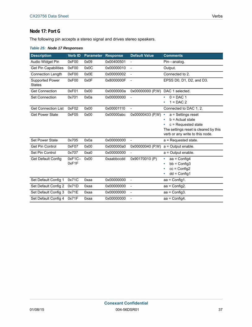
Node 17: Port GThe following pin accepts a stereo signal and drives stereo speakers.
Table 25: Node 17 Responses
Description Verb ID Parameter Response Default Value CommentsAudio Widget Pin 0xF00 0x09 0x00400501 - Pin—analog.
Get Pin Capabilities 0xF00 0x0C 0x00000010 - Output.
Connection Length 0xF00 0x0E 0x00000002 - Connected to 2.
Supported Power States
0xF00 0x0F 0x8000000F - EPSS D0, D1, D2, and D3.
Get Connection 0xF01 0x00 0x0000000a 0x00000000 (P,W) DAC 1 selected.
Set Connection 0x701 0x0a 0x00000000 - • 0 = DAC 1• 1 = DAC 2
Get Connection List 0xF02 0x00 0x00001110 - Connected to DAC 1, 2.
Get Power State 0xF05 0x00 0x00000abc 0x00000433 (P,W) • a = Settings reset• b = Actual state• c = Requested stateThe settings reset is cleared by this verb or any write to this node.
Set Power State 0x705 0x0a 0x00000000 - a = Requested state.
Get Pin Control 0xF07 0x00 0x000000a0 0x00000040 (P,W) a = Output enable.
Set Pin Control 0x707 0xa0 0x00000000 - a = Output enable.
Get Default Config 0xF1C–0xF1F
0x00 0xaabbccdd 0x90170010 (P) • aa = Config4• bb = Config3• cc = Config2• dd = Config1
Set Default Config 1 0x71C 0xaa 0x00000000 - aa = Config1.
Set Default Config 2 0x71D 0xaa 0x00000000 - aa = Config2.
Set Default Config 3 0x71E 0xaa 0x00000000 - aa = Config3.
Set Default Config 4 0x71F 0xaa 0x00000000 - aa = Config4.
Conexant Confidential01/08/15 004-56DSR01 37
CX20756 Data Sheet Verbs
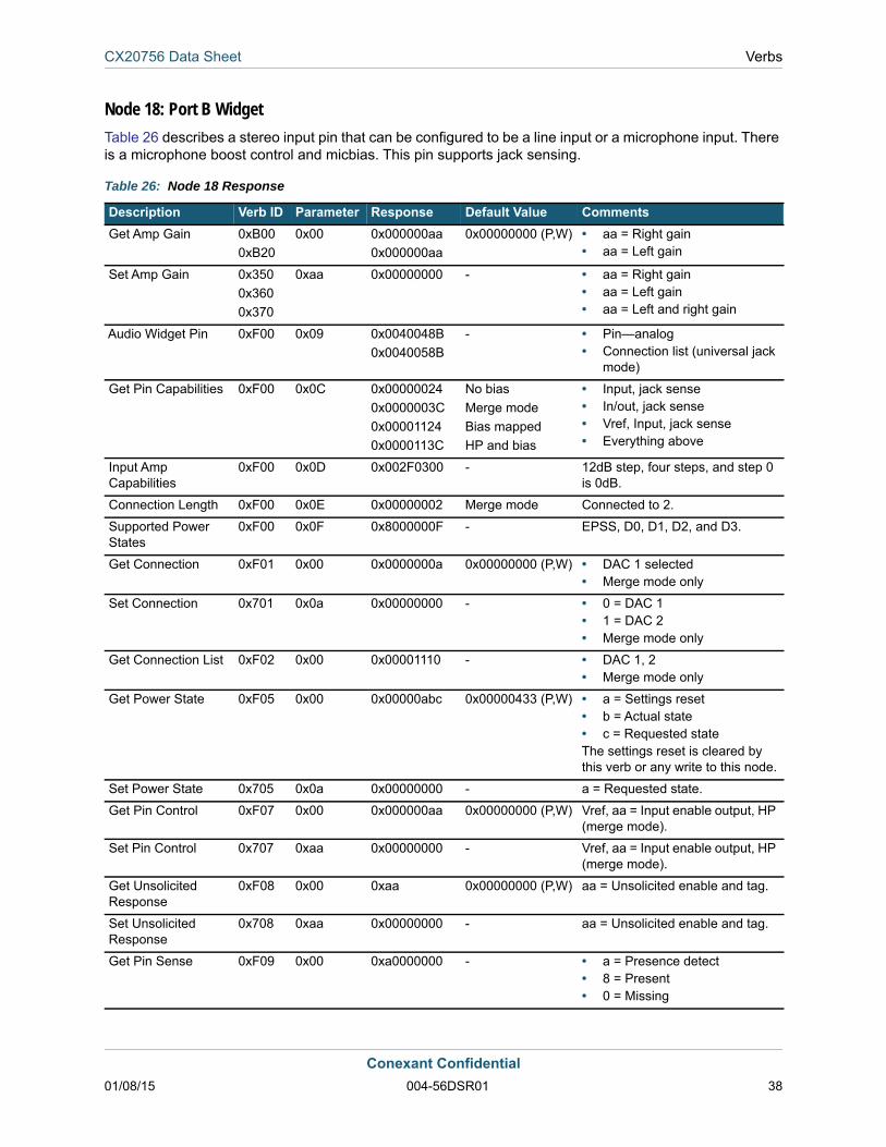
Node 18: Port B WidgetTable 26 describes a stereo input pin that can be configured to be a line input or a microphone input. There is a microphone boost control and micbias. This pin supports jack sensing.
Table 26: Node 18 Response
Description Verb ID Parameter Response Default Value CommentsGet Amp Gain 0xB00
0xB200x00 0x000000aa
0x000000aa0x00000000 (P,W) • aa = Right gain
• aa = Left gain
Set Amp Gain 0x3500x3600x370
0xaa 0x00000000 - • aa = Right gain• aa = Left gain• aa = Left and right gain
Audio Widget Pin 0xF00 0x09 0x0040048B0x0040058B
- • Pin—analog• Connection list (universal jack
mode)
Get Pin Capabilities 0xF00 0x0C 0x000000240x0000003C0x000011240x0000113C
No biasMerge modeBias mappedHP and bias
• Input, jack sense• In/out, jack sense• Vref, Input, jack sense• Everything above
Input Amp Capabilities
0xF00 0x0D 0x002F0300 - 12dB step, four steps, and step 0 is 0dB.
Connection Length 0xF00 0x0E 0x00000002 Merge mode Connected to 2.
Supported Power States
0xF00 0x0F 0x8000000F - EPSS, D0, D1, D2, and D3.
Get Connection 0xF01 0x00 0x0000000a 0x00000000 (P,W) • DAC 1 selected• Merge mode only
Set Connection 0x701 0x0a 0x00000000 - • 0 = DAC 1• 1 = DAC 2• Merge mode only
Get Connection List 0xF02 0x00 0x00001110 - • DAC 1, 2• Merge mode only
Get Power State 0xF05 0x00 0x00000abc 0x00000433 (P,W) • a = Settings reset• b = Actual state• c = Requested stateThe settings reset is cleared by this verb or any write to this node.
Set Power State 0x705 0x0a 0x00000000 - a = Requested state.
Get Pin Control 0xF07 0x00 0x000000aa 0x00000000 (P,W) Vref, aa = Input enable output, HP (merge mode).
Set Pin Control 0x707 0xaa 0x00000000 - Vref, aa = Input enable output, HP (merge mode).
Get Unsolicited Response
0xF08 0x00 0xaa 0x00000000 (P,W) aa = Unsolicited enable and tag.
Set Unsolicited Response
0x708 0xaa 0x00000000 - aa = Unsolicited enable and tag.
Get Pin Sense 0xF09 0x00 0xa0000000 - • a = Presence detect• 8 = Present• 0 = Missing
Conexant Confidential01/08/15 004-56DSR01 38
CX20756 Data Sheet Verbs
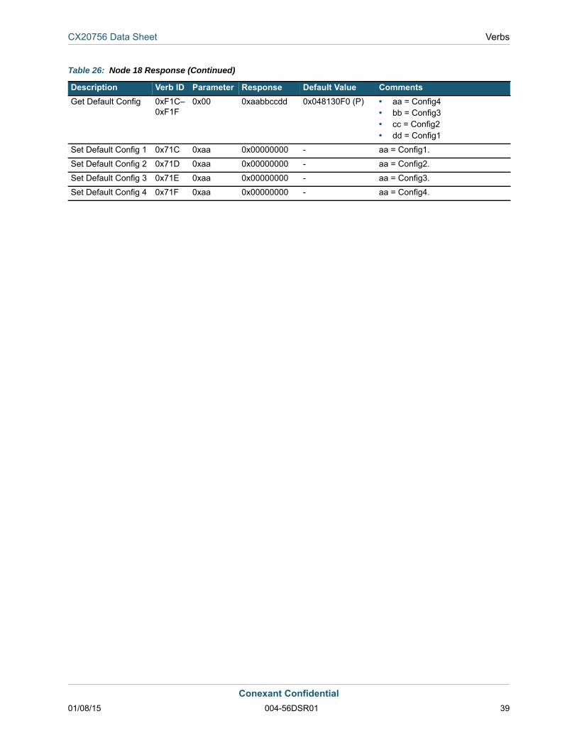
Get Default Config 0xF1C–0xF1F
0x00 0xaabbccdd 0x048130F0 (P) • aa = Config4• bb = Config3• cc = Config2• dd = Config1
Set Default Config 1 0x71C 0xaa 0x00000000 - aa = Config1.
Set Default Config 2 0x71D 0xaa 0x00000000 - aa = Config2.
Set Default Config 3 0x71E 0xaa 0x00000000 - aa = Config3.
Set Default Config 4 0x71F 0xaa 0x00000000 - aa = Config4.
Table 26: Node 18 Response (Continued)
Description Verb ID Parameter Response Default Value Comments
Conexant Confidential01/08/15 004-56DSR01 39
CX20756 Data Sheet Verbs
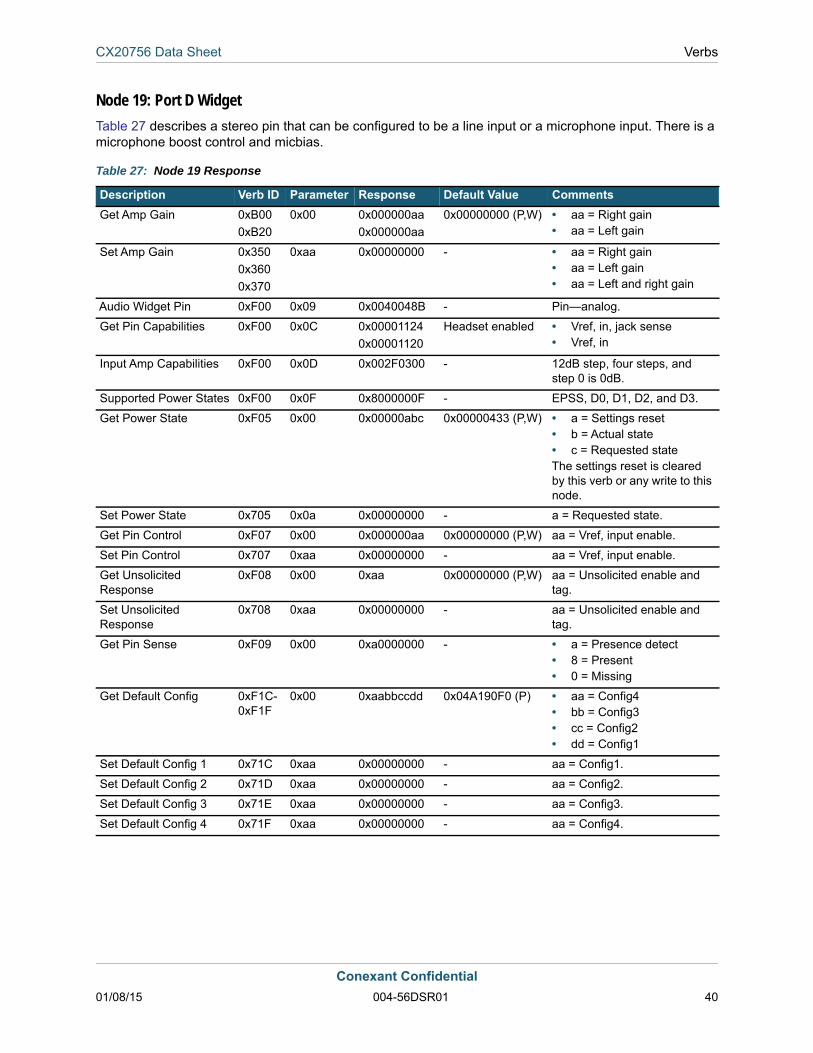
Node 19: Port D WidgetTable 27 describes a stereo pin that can be configured to be a line input or a microphone input. There is a microphone boost control and micbias.
Table 27: Node 19 Response
Description Verb ID Parameter Response Default Value CommentsGet Amp Gain 0xB00
0xB200x00 0x000000aa
0x000000aa0x00000000 (P,W) • aa = Right gain
• aa = Left gain
Set Amp Gain 0x3500x3600x370
0xaa 0x00000000 - • aa = Right gain• aa = Left gain• aa = Left and right gain
Audio Widget Pin 0xF00 0x09 0x0040048B - Pin—analog.
Get Pin Capabilities 0xF00 0x0C 0x000011240x00001120
Headset enabled • Vref, in, jack sense• Vref, in
Input Amp Capabilities 0xF00 0x0D 0x002F0300 - 12dB step, four steps, and step 0 is 0dB.
Supported Power States 0xF00 0x0F 0x8000000F - EPSS, D0, D1, D2, and D3.
Get Power State 0xF05 0x00 0x00000abc 0x00000433 (P,W) • a = Settings reset• b = Actual state• c = Requested stateThe settings reset is cleared by this verb or any write to this node.
Set Power State 0x705 0x0a 0x00000000 - a = Requested state.
Get Pin Control 0xF07 0x00 0x000000aa 0x00000000 (P,W) aa = Vref, input enable.
Set Pin Control 0x707 0xaa 0x00000000 - aa = Vref, input enable.
Get Unsolicited Response
0xF08 0x00 0xaa 0x00000000 (P,W) aa = Unsolicited enable and tag.
Set Unsolicited Response
0x708 0xaa 0x00000000 - aa = Unsolicited enable and tag.
Get Pin Sense 0xF09 0x00 0xa0000000 - • a = Presence detect• 8 = Present• 0 = Missing
Get Default Config 0xF1C-0xF1F
0x00 0xaabbccdd 0x04A190F0 (P) • aa = Config4• bb = Config3• cc = Config2• dd = Config1
Set Default Config 1 0x71C 0xaa 0x00000000 - aa = Config1.
Set Default Config 2 0x71D 0xaa 0x00000000 - aa = Config2.
Set Default Config 3 0x71E 0xaa 0x00000000 - aa = Config3.
Set Default Config 4 0x71F 0xaa 0x00000000 - aa = Config4.
Conexant Confidential01/08/15 004-56DSR01 40
CX20756 Data Sheet Verbs
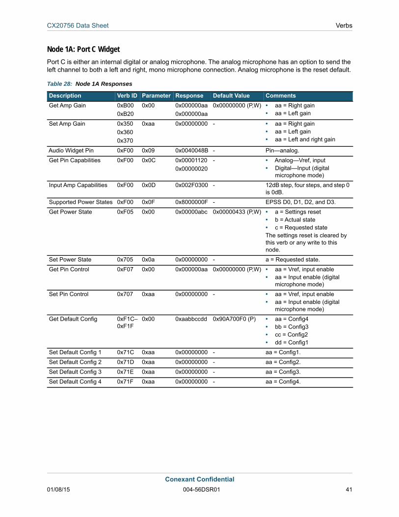
Node 1A: Port C WidgetPort C is either an internal digital or analog microphone. The analog microphone has an option to send the left channel to both a left and right, mono microphone connection. Analog microphone is the reset default.
Table 28: Node 1A Responses
Description Verb ID Parameter Response Default Value CommentsGet Amp Gain 0xB00
0xB200x00 0x000000aa
0x000000aa0x00000000 (P,W) • aa = Right gain
• aa = Left gain
Set Amp Gain 0x3500x3600x370
0xaa 0x00000000 - • aa = Right gain• aa = Left gain• aa = Left and right gain
Audio Widget Pin 0xF00 0x09 0x0040048B - Pin—analog.
Get Pin Capabilities 0xF00 0x0C 0x000011200x00000020
- • Analog—Vref, input• Digital—Input (digital
microphone mode)
Input Amp Capabilities 0xF00 0x0D 0x002F0300 - 12dB step, four steps, and step 0 is 0dB.
Supported Power States 0xF00 0x0F 0x8000000F - EPSS D0, D1, D2, and D3.
Get Power State 0xF05 0x00 0x00000abc 0x00000433 (P,W) • a = Settings reset• b = Actual state• c = Requested stateThe settings reset is cleared by this verb or any write to this node.
Set Power State 0x705 0x0a 0x00000000 - a = Requested state.
Get Pin Control 0xF07 0x00 0x000000aa 0x00000000 (P,W) • aa = Vref, input enable• aa = Input enable (digital
microphone mode)
Set Pin Control 0x707 0xaa 0x00000000 - • aa = Vref, input enable• aa = Input enable (digital
microphone mode)
Get Default Config 0xF1C–0xF1F
0x00 0xaabbccdd 0x90A700F0 (P) • aa = Config4• bb = Config3• cc = Config2• dd = Config1
Set Default Config 1 0x71C 0xaa 0x00000000 - aa = Config1.
Set Default Config 2 0x71D 0xaa 0x00000000 - aa = Config2.
Set Default Config 3 0x71E 0xaa 0x00000000 - aa = Config3.
Set Default Config 4 0x71F 0xaa 0x00000000 - aa = Config4.
Conexant Confidential01/08/15 004-56DSR01 41
CX20756 Data Sheet Ordering Information
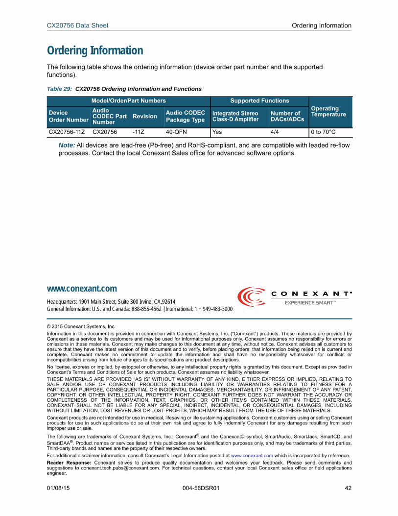
Ordering InformationThe following table shows the ordering information (device order part number and the supported functions).
Note: All devices are lead-free (Pb-free) and RoHS-compliant, and are compatible with leaded re-flow processes. Contact the local Conexant Sales office for advanced software options.
Table 29: CX20756 Ordering Information and Functions
Model/Order/Part Numbers Supported FunctionsOperating TemperatureDevice
Order NumberAudio CODEC Part Number
Revision Audio CODECPackage Type
Integrated Stereo Class-D Amplifier
Number of DACs/ADCs
CX20756-11Z CX20756 -11Z 40-QFN Yes 4/4 0 to 70°C
01/08/15 004-56DSR01 42
© 2015 Conexant Systems, Inc.Information in this document is provided in connection with Conexant Systems, Inc. (“Conexant”) products. These materials are provided byConexant as a service to its customers and may be used for informational purposes only. Conexant assumes no responsibility for errors oromissions in these materials. Conexant may make changes to this document at any time, without notice. Conexant advises all customers toensure that they have the latest version of this document and to verify, before placing orders, that information being relied on is current andcomplete. Conexant makes no commitment to update the information and shall have no responsibility whatsoever for conflicts orincompatibilities arising from future changes to its specifications and product descriptions. No license, express or implied, by estoppel or otherwise, to any intellectual property rights is granted by this document. Except as provided inConexant’s Terms and Conditions of Sale for such products, Conexant assumes no liability whatsoever. THESE MATERIALS ARE PROVIDED “AS IS” WITHOUT WARRANTY OF ANY KIND, EITHER EXPRESS OR IMPLIED, RELATING TOSALE AND/OR USE OF CONEXANT PRODUCTS INCLUDING LIABILITY OR WARRANTIES RELATING TO FITNESS FOR APARTICULAR PURPOSE, CONSEQUENTIAL OR INCIDENTAL DAMAGES, MERCHANTABILITY, OR INFRINGEMENT OF ANY PATENT,COPYRIGHT, OR OTHER INTELLECTUAL PROPERTY RIGHT. CONEXANT FURTHER DOES NOT WARRANT THE ACCURACY ORCOMPLETENESS OF THE INFORMATION, TEXT, GRAPHICS, OR OTHER ITEMS CONTAINED WITHIN THESE MATERIALS.CONEXANT SHALL NOT BE LIABLE FOR ANY SPECIAL, INDIRECT, INCIDENTAL, OR CONSEQUENTIAL DAMAGES, INCLUDINGWITHOUT LIMITATION, LOST REVENUES OR LOST PROFITS, WHICH MAY RESULT FROM THE USE OF THESE MATERIALS. Conexant products are not intended for use in medical, lifesaving or life sustaining applications. Conexant customers using or selling Conexantproducts for use in such applications do so at their own risk and agree to fully indemnify Conexant for any damages resulting from suchimproper use or sale.
The following are trademarks of Conexant Systems, Inc.: Conexant® and the Conexant© symbol, SmartAudio, SmartJack, SmartCD, andSmartDAA®. Product names or services listed in this publication are for identification purposes only, and may be trademarks of third parties.Third-party brands and names are the property of their respective owners.For additional disclaimer information, consult Conexant’s Legal Information posted at www.conexant.com which is incorporated by reference. Reader Response: Conexant strives to produce quality documentation and welcomes your feedback. Please send comments andsuggestions to [email protected]. For technical questions, contact your local Conexant sales office or field applicationsengineer.
www.conexant.comHeadquarters: 1901 Main Street, Suite 300 Irvine, CA,92614General Information: U.S. and Canada: 888-855-4562 | International: 1 + 949-483-3000