Embed Size (px)
Citation preview

ALC272 (PN: ALC272-GR)
4 CHANNEL HIGH DEFINITION AUDIO CODEC
DATASHEET
Rev. 1.0 21 May 2008
Track ID: JATR-1076-21
Realtek Semiconductor Corp. No. 2, Innovation Road II, Hsinchu Science Park, Hsinchu 300, Taiwan Tel.: +886-3-578-0211. Fax: +886-3-577-6047 www.realtek.com.tw

ALC272 Datasheet
4 Channel High Definition Audio Codec ii Track ID: JATR-1076-21 Rev. 1.0
COPYRIGHT ©2008 Realtek Semiconductor Corp. All rights reserved. No part of this document may be reproduced, transmitted, transcribed, stored in a retrieval system, or translated into any language in any form or by any means without the written permission of Realtek Semiconductor Corp.
DISCLAIMER Realtek provides this document “as is”, without warranty of any kind, neither expressed nor implied, including, but not limited to, the particular purpose. Realtek may make improvements and/or changes in this document or in the product described in this document at any time. This document could include technical inaccuracies or typographical errors.
TRADEMARKS Realtek is a trademark, of Realtek Semiconductor Corporation. Other names mentioned in this document are trademarks/registered trademarks of their respective owners.
USING THIS DOCUMENT This document is intended for the hardware and software engineer’s general information on the Realtek ALC272 Audio Codec IC.
Though every effort has been made to ensure that this document is current and accurate, more information may have become available subsequent to the production of this guide. In that event, please contact your Realtek representative for additional information that may help in the development process.
REVISION HISTORY Revision Release Date Summary
1.0 2008/05/21 First release.

ALC272 Datasheet
4 Channel High Definition Audio Codec iii Track ID: JATR-1076-21 Rev. 1.0
Table of Contents 1. GENERAL DESCRIPTION..............................................................................................................................................1
2. FEATURES.........................................................................................................................................................................2 2.1. HARDWARE FEATURES ................................................................................................................................................2 2.2. SOFTWARE FEATURES..................................................................................................................................................3
3. SYSTEM APPLICATIONS...............................................................................................................................................4
4. BLOCK DIAGRAM...........................................................................................................................................................5
5. PIN ASSIGNMENTS .........................................................................................................................................................6 5.1. PACKAGE AND VERSION IDENTIFICATION....................................................................................................................6
6. PIN DESCRIPTIONS.........................................................................................................................................................7 6.1. DIGITAL I/O PINS .........................................................................................................................................................7 6.2. ANALOG I/O PINS ........................................................................................................................................................7 6.3. FILTER/REFERENCE/NOT CONNECT .............................................................................................................................8 6.4. POWER/GROUND..........................................................................................................................................................8
7. HIGH DEFINITION AUDIO LINK PROTOCOL .........................................................................................................9 7.1. LINK SIGNALS..............................................................................................................................................................9
7.1.1. Signal Definitions .................................................................................................................................................10 7.1.2. Signaling Topology...............................................................................................................................................11
7.2. FRAME COMPOSITION ................................................................................................................................................12 7.2.1. Outbound Frame – Single SDO............................................................................................................................12 7.2.2. Outbound Frame – Multiple SDOs.......................................................................................................................13 7.2.3. Inbound Frame – Single SDI ................................................................................................................................14 7.2.4. Inbound Frame – Multiple SDIs...........................................................................................................................15 7.2.5. Variable Sample Rates .........................................................................................................................................15
7.3. RESET AND INITIALIZATION .......................................................................................................................................18 7.3.1. Link Reset .............................................................................................................................................................18 7.3.2. Codec Reset ..........................................................................................................................................................19 7.3.3. Codec Initialization Sequence ..............................................................................................................................20
7.4. VERB AND RESPONSE FORMAT ..................................................................................................................................20 7.4.1. Command Verb Format........................................................................................................................................20 7.4.2. Response Format ..................................................................................................................................................23 7.4.3. Double Function Reset .........................................................................................................................................23
7.5. POWER MANAGEMENT...............................................................................................................................................24 8. SUPPORTED VERBS AND PARAMETERS................................................................................................................26
8.1. VERB – GET PARAMETERS (VERB ID=F00H).............................................................................................................26 8.1.1. Parameter – Vendor ID (Verb ID=F00h, Parameter ID=00h)............................................................................26 8.1.2. Parameter – Revision ID (Verb ID=F00h, Parameter ID=02h)..........................................................................26 8.1.3. Parameter – Subordinate Node Count (Verb ID=F00h, Parameter ID=04h) .....................................................27 8.1.4. Parameter – Function Group Type (Verb ID=F00h, Parameter ID=05h) ..........................................................27 8.1.5. Parameter– Audio Function Capabilities (Verb ID=F00h, Parameter ID=08h) ................................................27 8.1.6. Parameter – Audio Widget Capabilities (Verb ID=F00h, Parameter ID=09h) ..................................................28 8.1.7. Parameter – Supported PCM Size, Rates (Verb ID=F00h, Parameter ID=0Ah) ................................................29 8.1.8. Parameter – Supported Stream Formats (Verb ID=F00h, Parameter ID=0Bh) .................................................30 8.1.9. Parameter – Pin Capabilities (Verb ID=F00h, Parameter ID=0Ch) ..................................................................30 8.1.10. Parameter– Amplifier Capabilities (Verb ID=F00h, Input Amplifier Parameter ID=0Dh).........................31

ALC272 Datasheet
4 Channel High Definition Audio Codec iv Track ID: JATR-1076-21 Rev. 1.0
8.1.11. Parameter – Amplifier Capabilities (Verb ID=F00h, Output Amplifier Parameter ID=12h) ........................31 8.1.12. Parameter – Connect List Length (Verb ID=F00h, Parameter ID=0Eh) .......................................................32 8.1.13. Parameter – Supported Power States (Verb ID=F00h, Parameter ID=0Fh) .................................................32 8.1.14. Parameter – Processing Capabilities (Verb ID=F00h, Parameter ID=10h)..................................................33 8.1.15. Parameter – GPIO Capabilities (Verb ID=F00h, Parameter ID=11h)..........................................................33 8.1.16. Parameter – Volume Knob Capabilities (Verb ID=F00h, Parameter ID=13h)..............................................33
8.2. VERB – GET CONNECTION SELECT CONTROL (VERB ID=F01H) ................................................................................34 8.3. VERB – SET CONNECTION SELECT (VERB ID=701H) .................................................................................................35 8.4. VERB – GET CONNECTION LIST ENTRY (VERB ID=F02H) .........................................................................................35 8.5. VERB – GET PROCESSING STATE (VERB ID=F03H) ...................................................................................................40 8.6. VERB – SET PROCESSING STATE (VERB ID=703H) ....................................................................................................40 8.7. VERB – GET COEFFICIENT INDEX (VERB ID=DH)......................................................................................................41 8.8. VERB – SET COEFFICIENT INDEX (VERB ID=5H) .......................................................................................................41 8.9. VERB – GET PROCESSING COEFFICIENT (VERB ID=CH) ............................................................................................41 8.10. VERB – SET PROCESSING COEFFICIENT (VERB ID=4H)..............................................................................................42 8.11. VERB – GET AMPLIFIER GAIN (VERB ID=BH) ...........................................................................................................42 8.12. VERB – SET AMPLIFIER GAIN (VERB ID=3H) ............................................................................................................45 8.13. VERB – GET CONVERTER FORMAT (VERB ID=AH)....................................................................................................46 8.14. VERB – SET CONVERTER FORMAT (VERB ID=2H) .....................................................................................................47 8.15. VERB – GET POWER STATE (VERB ID=F05H)............................................................................................................48 8.16. VERB – SET POWER STATE (VERB ID=705H) ............................................................................................................49 8.17. VERB – GET CONVERTER STREAM, CHANNEL (VERB ID=F06H) ...............................................................................49 8.18. VERB – SET CONVERTER STREAM, CHANNEL (VERB ID=706H) ................................................................................50 8.19. VERB – GET PIN WIDGET CONTROL (VERB ID=F07H) ..............................................................................................50 8.20. VERB – SET PIN WIDGET CONTROL (VERB ID=707H) ...............................................................................................51 8.21. VERB – GET UNSOLICITED RESPONSE CONTROL (VERB ID=F08H) ...........................................................................52 8.22. VERB – SET UNSOLICITED RESPONSE CONTROL (VERB ID=708H) ............................................................................52 8.23. VERB – GET PIN SENSE (VERB ID=F09H)..................................................................................................................53 8.24. VERB – EXECUTE PIN SENSE (VERB ID=709H)..........................................................................................................53 8.25. VERB – GET CONFIGURATION DEFAULT (VERB ID=F1CH/F1DH/F1EH/F1FH).........................................................54 8.26. VERB – SET CONFIGURATION DEFAULT BYTES 0, 1, 2, 3 (VERB ID=71CH/71DH/71EH/71FH).................................54 8.27. VERB – GET BEEP GENERATOR (VERB ID=F0AH) ...................................................................................................55 8.28. VERB – SET BEEP GENERATOR (VERB ID=70AH) ....................................................................................................55 8.29. VERB – GET GPIO DATA (VERB ID= F15H) ..............................................................................................................56 8.30. VERB – SET GPIO DATA (VERB ID= 715H)...............................................................................................................56 8.31. VERB – GET GPIO ENABLE MASK (VERB ID=F16H).................................................................................................57 8.32. VERB – SET GPIO ENABLE MASK (VERB ID=716H) .................................................................................................57 8.33. VERB – GET GPIO DIRECTION (VERB ID=F17H).......................................................................................................58 8.34. VERB – SET GPIO DIRECTION (VERB ID=717H) .......................................................................................................58 8.35. VERB – GET GPIO UNSOLICITED RESPONSE ENABLE MASK (VERB ID=F19H) .......................................................59 8.36. VERB – SET GPIO UNSOLICITED RESPONSE ENABLE MASK (VERB ID=719H) ........................................................59 8.37. VERB – GET DIGITAL CONVERTER CONTROL 1 & CONTROL 2 (VERB ID= F0DH, F0EH)..........................................60 8.38. VERB – SET DIGITAL CONVERTER CONTROL 1 & CONTROL 2 (VERB ID=70DH, 70EH)............................................61 8.39. VERB – GET SUBSYSTEM ID [31:0] (VERB ID=F20H/F21H/D22H/F23H) ..................................................................62 8.40. VERB – SET SUBSYSTEM ID [31:0] (VERB ID=723H/722H/721H/720H FOR [31:24]/[23:16]//[15:8]/[7:0]) ...............62 8.41. VERB – GET/SET EAPD CONTROL (VERB ID=F0CH FOR GET, 70CH FOR SET).........................................................63 8.42. VERB – FUNCTION RESET (VERB ID=7FFH) ..............................................................................................................64
9. ELECTRICAL CHARACTERISTICS ..........................................................................................................................65 9.1. DC CHARACTERISTICS...............................................................................................................................................65
9.1.1. Absolute Maximum Ratings ..................................................................................................................................65 9.1.2. Threshold Voltage ................................................................................................................................................65 9.1.3. SPDIF Output Characteristics .............................................................................................................................66 9.1.4. Digital Filter Characteristics ...............................................................................................................................66
9.2. AC CHARACTERISTICS...............................................................................................................................................67

ALC272 Datasheet
4 Channel High Definition Audio Codec v Track ID: JATR-1076-21 Rev. 1.0
9.2.1. Link Reset and Initialization Timing.....................................................................................................................67 9.2.2. Link Timing Parameters at the Codec ..................................................................................................................68 9.2.3. SPDIF Output Timing...........................................................................................................................................69 9.2.4. Test Mode .............................................................................................................................................................69
9.3. ANALOG PERFORMANCE............................................................................................................................................70 10. APPLICATION CIRCUITS .......................................................................................................................................71
10.1. FILTER CONNECTION .................................................................................................................................................71 10.2. ONBOARD FRONT PANEL HEADER CONNECTION AND FRONT PANEL I/O..................................................................72 10.3. POWER SUPPLY AND ANALOG INPUT/OUTPUT CONNECTION .....................................................................................73 10.4. OPTIONAL SPDIF OUTPUT.........................................................................................................................................74
11. MECHANICAL DIMENSIONS.................................................................................................................................75
12. ORDERING INFORMATION...................................................................................................................................76

ALC272 Datasheet
4 Channel High Definition Audio Codec vi Track ID: JATR-1076-21 Rev. 1.0
List of Tables TABLE 1. DIGITAL I/O PINS..........................................................................................................................................................7 TABLE 2. ANALOG I/O PINS .........................................................................................................................................................7 TABLE 3. FILTER/REFERENCE ......................................................................................................................................................8 TABLE 4. POWER/GROUND...........................................................................................................................................................8 TABLE 5. LINK RESET# ............................................................................................................................................................10 TABLE 6. HDA SIGNAL DEFINITIONS.........................................................................................................................................10 TABLE 7. DEFINED SAMPLE RATE AND TRANSMISSION RATE....................................................................................................16 TABLE 8. 48KHZ VARIABLE RATE OF DELIVERY TIMING ..........................................................................................................16 TABLE 9. 44.1KHZ VARIABLE RATE OF DELIVERY TIMING .......................................................................................................17 TABLE 10. 40-BIT COMMANDS IN 4-BIT VERB FORMAT .............................................................................................................20 TABLE 11. 40-BIT COMMANDS IN 12-BIT VERB FORMAT ...........................................................................................................20 TABLE 12. SUPPORTED COMMANDS ............................................................................................................................................21 TABLE 13. SUPPORTED PARAMETERS..........................................................................................................................................22 TABLE 14. SOLICITED RESPONSE FORMAT ..................................................................................................................................23 TABLE 15. UNSOLICITED RESPONSE FORMAT .............................................................................................................................23 TABLE 16. SYSTEM POWER STATE DEFINITIONS .........................................................................................................................25 TABLE 17. POWER CONTROLS IN NID 01H..................................................................................................................................25 TABLE 18. POWERED DOWN CONDITIONS...................................................................................................................................25 TABLE 19. VERB – GET PARAMETERS (VERB ID=F00H).............................................................................................................26 TABLE 20. PARAMETER – VENDOR ID (VERB ID=F00H, PARAMETER ID=00H)..........................................................................26 TABLE 21. PARAMETER – REVISION ID (VERB ID=F00H, PARAMETER ID=02H) ........................................................................26 TABLE 22. PARAMETER – SUBORDINATE NODE COUNT (VERB ID=F00H, PARAMETER ID=04H) ...............................................27 TABLE 23. PARAMETER – FUNCTION GROUP TYPE (VERB ID=F00H, PARAMETER ID=05H) ......................................................27 TABLE 24. PARAMETER – AUDIO FUNCTION CAPABILITIES (VERB ID=F00H, PARAMETER ID=08H)..........................................27 TABLE 25. PARAMETER – AUDIO WIDGET CAPABILITIES (VERB ID=F00H, PARAMETER ID=09H).............................................28 TABLE 26. PARAMETER – SUPPORTED PCM SIZE, RATES (VERB ID=F00H, PARAMETER ID=0AH) ...........................................29 TABLE 27. PARAMETER – SUPPORTED STREAM FORMATS (VERB ID=F00H, PARAMETER ID=0BH)...........................................30 TABLE 28. PARAMETER – PIN CAPABILITIES (VERB ID=F00H, PARAMETER ID=0CH) ...............................................................30 TABLE 29. PARAMETER – AMPLIFIER CAPABILITIES (VERB ID=F00H, INPUT AMPLIFIER PARAMETER ID=0DH).......................31 TABLE 30. PARAMETER – AMPLIFIER CAPABILITIES (VERB ID=F00H, OUTPUT AMPLIFIER PARAMETER ID=12H) ....................31 TABLE 31. PARAMETER – CONNECT LIST LENGTH (VERB ID=F00H, PARAMETER ID=0EH) ......................................................32 TABLE 32. PARAMETER – SUPPORTED POWER STATES (VERB ID=F00H, PARAMETER ID=0FH) ................................................32 TABLE 33. PARAMETER – PROCESSING CAPABILITIES (VERB ID=F00H, PARAMETER ID=10H)..................................................33 TABLE 34. PARAMETER – GPIO CAPABILITIES (VERB ID=F00H, PARAMETER ID=11H) ............................................................33 TABLE 35. PARAMETER – VOLUME KNOB CAPABILITIES (VERB ID=F00H, PARAMETER ID=13H) .............................................33 TABLE 36. VERB – GET CONNECTION SELECT CONTROL (VERB ID=F01H) ................................................................................34 TABLE 37. VERB – SET CONNECTION SELECT (VERB ID=701H) .................................................................................................35 TABLE 38. VERB – GET CONNECTION LIST ENTRY (VERB ID=F02H) .........................................................................................35 TABLE 39. VERB – GET PROCESSING STATE (VERB ID=F03H) ...................................................................................................40 TABLE 40. VERB – SET PROCESSING STATE (VERB ID=703H) ....................................................................................................40 TABLE 41. VERB – GET COEFFICIENT INDEX (VERB ID=DH)......................................................................................................41 TABLE 42. VERB – SET COEFFICIENT INDEX (VERB ID=5H) .......................................................................................................41 TABLE 43. VERB – GET PROCESSING COEFFICIENT (VERB ID=CH) ............................................................................................41 TABLE 44. VERB – SET PROCESSING COEFFICIENT (VERB ID=4H)..............................................................................................42 TABLE 45. VERB – GET AMPLIFIER GAIN (VERB ID=BH) ...........................................................................................................42 TABLE 46. VERB – SET AMPLIFIER GAIN (VERB ID=3H).............................................................................................................45 TABLE 47. VERB – GET CONVERTER FORMAT (VERB ID=AH)....................................................................................................46 TABLE 48. GET CONVERTER FORMAT SUPPORT..........................................................................................................................46 TABLE 49. VERB – SET CONVERTER FORMAT (VERB ID=2H) .....................................................................................................47 TABLE 50. VERB – GET POWER STATE (VERB ID=F05H)............................................................................................................48 TABLE 51. VERB – SET POWER STATE (VERB ID=705H).............................................................................................................49 TABLE 52. VERB – GET CONVERTER STREAM, CHANNEL (VERB ID=F06H) ...............................................................................49

ALC272 Datasheet
4 Channel High Definition Audio Codec vii Track ID: JATR-1076-21 Rev. 1.0
TABLE 53. VERB – SET CONVERTER STREAM, CHANNEL (VERB ID=706H) ................................................................................50 TABLE 54. VERB – GET PIN WIDGET CONTROL (VERB ID=F07H) ..............................................................................................50 TABLE 55. VERB – SET PIN WIDGET CONTROL (VERB ID=707H) ...............................................................................................51 TABLE 56. VERB – GET UNSOLICITED RESPONSE CONTROL (VERB ID=F08H) ...........................................................................52 TABLE 57. VERB – SET UNSOLICITED RESPONSE CONTROL (VERB ID=708H) ............................................................................52 TABLE 58. VERB – GET PIN SENSE (VERB ID=F09H)..................................................................................................................53 TABLE 59. VERB – EXECUTE PIN SENSE (VERB ID=709H)..........................................................................................................53 TABLE 60. VERB – GET CONFIGURATION DEFAULT (VERB ID=F1CH/F1DH/F1EH/F1FH) .........................................................54 TABLE 61. VERB – SET CONFIGURATION DEFAULT BYTES 0, 1, 2, 3 (VERB ID=71CH/71DH/71EH/71FH).................................54 TABLE 62. VERB – GET BEEP GENERATOR (VERB ID= F0AH) ..................................................................................................55 TABLE 63. VERB – SET BEEP GENERATOR (VERB ID= 70AH) ...................................................................................................55 TABLE 64. VERB – GET GPIO DATA (VERB ID= F15H) ..............................................................................................................56 TABLE 65. VERB – SET GPIO DATA (VERB ID= 715H) ...............................................................................................................56 TABLE 66. VERB – GET GPIO ENABLE MASK (VERB ID= F16H)................................................................................................57 TABLE 67. VERB – SET GPIO ENABLE MASK (VERB ID=716H) .................................................................................................57 TABLE 68. VERB – GET GPIO DIRECTION (VERB ID=F17H).......................................................................................................58 TABLE 69. VERB – SET GPIO DIRECTION (VERB ID=717H) .......................................................................................................58 TABLE 70. VERB – GET GPIO UNSOLICITED RESPONSE ENABLE MASK (VERB ID=F19H) .........................................................59 TABLE 71. VERB – SET GPIO UNSOLICITED RESPONSE ENABLE MASK (VERB ID=719H)..........................................................59 TABLE 72. VERB – GET DIGITAL CONVERTER CONTROL 1 & CONTROL 2 (VERB ID= F0DH, F0EH) ..........................................60 TABLE 73. VERB – SET DIGITAL CONVERTER CONTROL 1 & CONTROL 2 (VERB ID=70DH, 70EH) ............................................61 TABLE 74. VERB – GET SUBSYSTEM ID [31:0] (VERB ID=F20H/F21H/F22H/F23H) ...................................................................62 TABLE 75. VERB – SET SUBSYSTEM ID [31:0] (VERB ID=723H/722H/721H/720H FOR [31:24]/[23:16]//[15:8]/[7:0])................62 TABLE 76. VERB – GET EAPD CONTROL (VERB ID=F0CH) .......................................................................................................63 TABLE 77. VERB – SET EAPD CONTROL (VERB ID=70CH)........................................................................................................63 TABLE 78. VERB – FUNCTION RESET (VERB ID=7FFH) ..............................................................................................................64 TABLE 79. ABSOLUTE MAXIMUM RATINGS ................................................................................................................................65 TABLE 80. THRESHOLD VOLTAGE...............................................................................................................................................65 TABLE 81. SPDIF OUTPUT CHARACTERISTICS............................................................................................................................66 TABLE 82. DIGITAL FILTER CHARACTERISTICS ...........................................................................................................................66 TABLE 83. LINK RESET AND INITIALIZATION TIMING..................................................................................................................67 TABLE 84. LINK TIMING PARAMETERS AT THE CODEC ...............................................................................................................68 TABLE 85. SPDIF OUTPUT TIMING .............................................................................................................................................69 TABLE 86. ANALOG PERFORMANCE ............................................................................................................................................70 TABLE 87. ORDERING INFORMATION ..........................................................................................................................................76
ALC272 Datasheet
4 Channel High Definition Audio Codec viii Track ID: JATR-1076-21 Rev. 1.0
List of Figures FIGURE 1. BLOCK DIAGRAM ........................................................................................................................................................5 FIGURE 2. PIN ASSIGNMENTS .......................................................................................................................................................6 FIGURE 3. HDA LINK PROTOCOL.................................................................................................................................................9 FIGURE 4. BIT TIMING................................................................................................................................................................10 FIGURE 5. SIGNALING TOPOLOGY ..............................................................................................................................................11 FIGURE 6. SDO OUTBOUND FRAME...........................................................................................................................................12 FIGURE 7. SDO STREAM TAG IS INDICATED IN SYNC...............................................................................................................12 FIGURE 8. STRIPED STREAM ON MULTIPLE SDOS......................................................................................................................13 FIGURE 9. SDI INBOUND STREAM ..............................................................................................................................................14 FIGURE 10. SDI STREAM TAG AND DATA ...................................................................................................................................14 FIGURE 11. CODEC TRANSMITS DATA OVER MULTIPLE SDIS ....................................................................................................15 FIGURE 12. LINK RESET TIMING..................................................................................................................................................19 FIGURE 13. CODEC INITIALIZATION SEQUENCE...........................................................................................................................20 FIGURE 14. RESUME FROM EXTERNAL EVENT (WAKE-UP EVENT).............................................................................................24 FIGURE 15. LINK RESET AND INITIALIZATION TIMING ................................................................................................................67 FIGURE 16. LINK SIGNAL TIMING................................................................................................................................................68 FIGURE 17. OUTPUT TIMING........................................................................................................................................................69 FIGURE 18. FILTER CONNECTION ................................................................................................................................................71 FIGURE 19. ONBOARD FRONT PANEL HEADER CONNECTION AND FRONT PANEL I/O .................................................................72 FIGURE 20. ANALOG INPUT/OUTPUT CONNECTION.....................................................................................................................73 FIGURE 21. OPTIONAL SPDIF OUTPUT .......................................................................................................................................74

ALC272 Datasheet
4 Channel High Definition Audio Codec 1 Track ID: JATR-1076-21 Rev. 1.0
1. General Description The ALC272 is a High Definition Audio Codec that meets the current WLP3.10 (Windows Logo Program) audio requirements for Windows Vista systems.
Featuring two stereo DACs, two stereo ADCs, legacy analog input to analog output mixing, one stereo digital microphone converter, and two independent SPDIF output converters, the ALC272 provides a fully integrated audio solution for multimedia desktop and mobile PCs, and ultra mobile devices.
The ALC272 integrates two stereo ADCs and two stereo digital microphone converters to support simultaneous analog microphone recording and up to 4 channel digital microphone array recording, and features Acoustic Echo Cancellation (AEC), Beam Forming (BF), and Noise Suppression (NS) for voice applications.
Multiple analog IO (except MONO, PCBEEP, and HP-OUT) are input and output capable, and provide headphone amplifiers. Four linear headphone amplifiers are integrated to drive earphones on port-A, port-D, port-E and port-F. The fifth headphone amplifier on port-I (HPOUT) is designed to drive an earphone without the need for external DC blocking capacitors, reducing pop noise and enhancing sound quality.
The ALC272 provides two independent SPDIF outputs and supports 16/20/24-bit SPDIF output with a sampling rate of up to 192kHz, offering easy connection of PCs to high quality consumer electronic products such as digital decoders and speakers. In addition to the standard (primary) SPDIF output function, the ALC272 features another independent (secondary) SPDIF-OUT output and converters that transport digital audio output to a High Definition Media Interface (HDMI) transmitter (becoming more common in high-end PCs).
In addition to the audio functions, the ALC272 supports enhanced power management. Its power management design conforms to Intel’s Audio Codec low power state white paper and is ECR compliant, reducing power consumption when the audio function is not being used, and offering jack detection wake-up when the system is in power down state so as to extend battery life for mobile systems without sacrificing audio features.
The ALC272 supports host audio controller from the Intel ICH series chipset, and also from any other HDA compatible audio controller. With software utilities like Karaoke mode, environment emulation, multi-band software equalizer, dynamic range compressor and extender, optional Dolby® Digital Live, DTS® CONNECT™, Dolby® Home Theater, and SRS® programs, the ALC272 provides an excellent home entertainment package and game experience for PC users.

ALC272 Datasheet
4 Channel High Definition Audio Codec 2 Track ID: JATR-1076-21 Rev. 1.0
2. Features
2.1. Hardware Features Meets performance and function requirements for Microsoft WLP 3.10, and stricter performance
requirements for future WLP
Two stereo DAC support 16/20/24-bit PCM for two independent playback (multiple streaming)
Two stereo ADC supports 16/20/24-bit PCM format for two independent recording
All DACs support independent 44.1k/48k/96k/192kHz sample rate
All ADCs support independent 44.1k/48k/96k/192kHz sample rate
Two independent SPDIF outputs support 16/20/24-bit format and 44.1k/48k/88.2k/96k/192kHz rate
All analog jack ports except MONO, BEEP-IN and HP-OUT are stereo input and output re-tasking
Supports line level mono output
Supports analog PCBEEP input, and features an integrated digital BEEP generator
Support two stereo digital microphone input for microphone array AEC/BF application
Each stereo digital microphone interface has its own clock output to support independent sample rate
Supports legacy analog mixer architecture
Built-in five headphone amplifiers on port-A and port-D, port-E, port-F and port-I.
Headphone amplifier on port-I (HP-OUT) is designed to drive output without external DC blocking capacitors
Software selectable 2.5V and 3.2V reference output for microphone bias
Software selectable boost gain (+10/+20/+30dB) for analog microphone input
Two jack detection pins; each supports detection of up to 4 jacks
Supports two GPIO (General Purpose Input/Output) pins (pin sharing with digital microphone interface)
Supports EAPD (External Amplifier Power Down) control for external amplifier
Supports anti-pop mode when analog power AVDD is on and digital power is off
Supports 1.5V~3.3V scalable I/O for HD Audio link
48-pin LQFP ‘Green’ package

ALC272 Datasheet
4 Channel High Definition Audio Codec 3 Track ID: JATR-1076-21 Rev. 1.0
Jack detection function is supported when device is in power down mode (D3)
Independent secondary SPDIF converter and pin to output digital stream to HDMI transmitter
Intel low power ECR compliant, supports power status control for each analog converter and pin widgets, supports jack detection and wake up event in D3 mode
2.2. Software Features Meets Microsoft WLP 3.10 and future WLP audio requirements
WaveRT-based audio function driver for Windows Vista
EAX™ 1.0 & 2.0 compatible
Direct Sound 3D™ compatible
A3D™ compatible
I3DL2 compatible
Emulation of 26 sound environments to enhance gaming experience
Multi-band software equalizer and related tools are provided
Voice Cancellation and Key Shifting effect
Dynamic range control (expander, compressor and limiter) with adjustable parameters
Intuitive Configuration Panel (Realtek Audio Manager) to enhance user experience
Provides 10-foot GUI for easy menu navigation on Windows Media Center
Microphone Acoustic Echo Cancellation (AEC), Noise Suppression (NS), and Beam Forming (BF) technology for voice application
Smart multiple streaming operation
HDMI audio driver for AMD platform
Dolby® PCEE program™ (optional software feature)
DTS® CONNECT™ (optional software feature)
SRS® TrueSurround HD (optional software feature)

ALC272 Datasheet
4 Channel High Definition Audio Codec 4 Track ID: JATR-1076-21 Rev. 1.0
Fortemedia® SAM™ technology for voice processing (Beam Forming and Acoustic Echo Cancellation) (optional software feature)
3. System Applications
Desktop and mobile PCs
Ultra mobile devices

ALC272 Datasheet
4 Channel High Definition Audio Codec 5 Track ID: JATR-1076-21 Rev. 1.0
4. Block Diagram
Dig
ital I
nter
face
LIN
E1(
Port
-C)
LOU
T1(P
ort-D
)
S/PD
IF-O
UT1
Para
met
ers
1
BEE
P-IN
06h
MIC
1(Po
rt-B
)
Dig
ital C
onve
rter
0/10
/20/
30dB
gai
n in
4st
ep
PCM
-2
PCM
-1
S/PD
IF-O
UT
22h
02h
03h
14h
1Dh
1Ah
1Eh
O A:O
utpu
t w/A
mpl
ifier
BEE
P G
en
I/O
M
I/O
Boo
st
VO
LM
VO
LM
VO
LM
VO
LM
I/O
MA
MM
M
MM
MM
M MV
OL
M MV
OL
0Ch
0Dh
LOU
T1
LOU
T2
MMM
M
MM
MM
23h
VO
L
VO
L
M M
M
Sam
ple
rate
:44
.1k,
48k
, 96k
, 19
2k
S/PD
IF-O
UT2
Dig
ital C
onve
rter
S/PD
IF-O
UT
11h
Sam
ple
rate
:44
.1k,
48k
, 96k
, 19
2k
SP-O
UT1
DA
TA
SP-O
UT2
DA
TA
LIN
E A
DC
08h
SRC
DM
IC-1
/2D
MIC
Rec
ieve
r12
h
DM
IC-3
/4D
MIC
Rec
ieve
r13
h
DM
IC-C
LK1/
21.
576M
/2.0
48M
/3.0
72M
Clo
ck
M
VO
L: -1
6.5~
30dB
(1.5
dB/s
tep)
MIX
AD
C
09h
SRC
M
MO
NO
-OU
T(P
ort-
H)
17h
MO
NO
OM
M M0F
h/2
MO
NO
DM
IC-C
LK3/
41.
576M
/2.0
48M
/3.0
72M
Clo
ck
AD
CM
VO
L
AD
CM
VO
L
Boo
st
LOU
T2(P
ort-
A)
15h
I/O
MA
LOU
T1
LIN
E2(P
ort-E
)1B
hI/
O AM
Boo
st
MIC
2(Po
rt-F
)19
hI/
O AM
Boo
st
VO
LM
HP-
OU
T(P
ort-
I)21
hO
MLO
UT2
LOU
T1A
Sam
ple
rate
:44
.1k,
48k
, 96k
, 19
2k
0Bh
VO
L:-
64~0
dB(1
dB/S
tep)
DA
C
Sam
ple
rate
:44
.1k,
48k
, 96k
, 19
2kSR
C
SRC
DA
CLO
UT2
LOU
T1LO
UT2
LOU
T1LO
UT2 LO
UT2
LOU
T1LO
UT2
18h
SP-O
UT1
Dat
a
10h
SP-O
UT2
Dat
a
Rec
orde
d PC
M
Rec
orde
d PC
M
-34.
5~+1
2dB
(1.5
dB/S
tep)
Figure 1. Block Diagram

ALC272 Datasheet
4 Channel High Definition Audio Codec 6 Track ID: JATR-1076-21 Rev. 1.0
5. Pin Assignments
)
LOUT2-L(PORT-A-L)
NC
SPDIFO1
AVSS2
AVDD2LINE1- R ( - C- R
MIC2- L ( -F- L )
LINE2- L (PORT
-E- L)EAPD
JDREF
Sense A
MIC
1-V
RE
FO
VR
EF
AV
SS1
AV
DD
1
SD
AT
A-O
UT
BITC
LK
SD
AT
A-IN
SY
NC
RE
SE
T#
PC
BE
EP-
IN
MIC1- L ( - B- L )
DV
DD
DV
SS
DV
SS
DV
DD
-IO
LINE2-R ( -E-R)
MIC2-R ( -F- R)
MIC1- R ( - B- R)LINE1- L ( - C- L)
ALC272
LLLLLLL TXXXVSDMIC-CLK1/2
SPDIFO2
GP
IO0/
DM
IC-D
ATA
1/2
CB
PC
BN
CP
VE
EH
PO
UT-
R(P
OR
T-I-
R)
HP
OU
T-L
(PO
RT-
I-L)
L I NE2- V REFOMI C2- VREFOLI NE1- V REFO
MONO- OUT36 35 34 33 32 31 30 29 28 27 26 25
17
18
19
20
24
23
22
21
13
14
15
1644
43
42
41
37
38
39
40
48
47
46
45
1 2 3 4 5 6 7 8 9 10 11 12
PORT
PORTPORT
PORTPORT
PORTPORT
Sen
se B
LOUT2-R(PORT-A-R)
DMIC-CLK3/4
GP
IO1/
DM
IC-D
ATA
3/4
LOU
T1-L
(PO
RT-
D-L
)LO
UT1
-R (P
OR
T-D
-R)
Figure 2. Pin Assignments
5.1. Package and Version Identification Green package is indicated by a ‘G’ in the location marked ‘T’. The silicon version and step numbers are shown in the location marked ‘V’ and ‘S’.

ALC272 Datasheet
4 Channel High Definition Audio Codec 7 Track ID: JATR-1076-21 Rev. 1.0
6. Pin Descriptions
6.1. Digital I/O Pins Table 1. Digital I/O Pins
Name Type Pin Description Characteristic Definition RESET# I 11 H/W Reset Vt=0.5*DVDDIO SYNC I 10 Sample Sync (48KHz) Vt=0.5*DVDDIO BITCLK I 6 24MHz Bit Clock Input Vt=0.5*DVDDIO SDATA-OUT I 5 Serial TDM Data Input Vt=0.5*DVDDIO SDATA-IN O 8 Serial TDM Data Output In: Vt=0.5*DVDDIO
Out: VOH=DVDDIO, VOL=DVSS GPIO0 / DMIC-DATA1/2
IO 2 General Purpose Input/Output 0 / Data Input for Digital Mic1/2
In: Vt=0.5*DVDD; Out: VOH=DVDD, VOL=DVSS / Shared with the digital MIC input data.
GPIO1 / DMIC-DATA3/4
IO 3 General Purpose Input/Output 1/ Data Input for Digital Mic3/4
In: Vt=0.5*DVDD; Out: VOH=DVDD, VOL=DVSS / Shared with the digital MIC input data.
EAPD O 47 External Amplifier Power Down VOH=DVDDIO, VOL=DVSS SPDIFO1 O 48 SPDIF Output 1 Output has 12 mA@75Ω driving capability. SPDIFO2 O 45 SPDIF Output 2 Output has 12 mA@75Ω driving capability. DMIC-CLK3/4 O 44 Clock Output for Digital Mic3/4 3.072M / 1.536M / 2.048M Hz DMIC-CLK1/2 O 46 Clock Output for Digital Mic1/2 3.072M / 1.536M / 2.048M Hz Total: 12 Pins
6.2. Analog I/O Pins Table 2. Analog I/O Pins
Name Type Pin Description Characteristic Definition LINE2-L IO 14 2nd Line Input Left Channel Analog input/output, default is input (PORT-E-L) LINE2-R IO 15 2nd Line Input Right Channel Analog input/output, default is input (PORT-E-R) MIC2-L IO 16 2nd Stereo Microphone Input Left
Channel Analog input/output, default is input (PORT-F-L)
MIC2-R IO 17 2nd Stereo Microphone Input Right Channel
Analog input/output, default is input (PORT-F-R)
MIC1-L IO 21 1st Stereo Microphone Input Left Channel
Analog input/output, default is input (PORT-B-L)
MIC1-R IO 22 1st Stereo Microphone Input Right Channel
Analog input/output, default is input (PORT-B-R)
LINE1-L IO 23 1st Line Input Left Channel Analog input/output, default is input (PORT-C-L) LINE1-R IO 24 1st Line Input Right Channel Analog input/output, default is input (PORT-C-R) PCBEEP-IN I 12 External PCBEEP Input Analog input, 1.6Vrms of full-scale input HPOUT-R O 32 Headphone Out Right Channel Analog output (PORT-I-R) HPOUT-L O 33 Headphone Out Left Channel Analog output (PORT-I-L) LOUT1-L IO 35 LOUT1 Output Left Channel Analog output (PORT-D-L) LOUT1-R IO 36 LOUT1 Output Right Channel Analog output (PORT-D-R)

ALC272 Datasheet
4 Channel High Definition Audio Codec 8 Track ID: JATR-1076-21 Rev. 1.0
Name Type Pin Description Characteristic Definition MONO-OUT O 37 MONO-OUT Analog output (PORT-H) LOUT2-L IO 39 LOUT2 Left Channel Analog output (PORT-A-L) LOUT2-R IO 41 LOUT2 Right Channel Analog output (PORT-A-R) Sense A I 13 Jack Detect Pin 1 Jack resistor network (5.1k, 10k, 20K, 39.2k) with
1% accuracy Sense B I 34 Jack Detect Pin 2 Jack resistor network (5.1k, 10k, 20K, 39.2k) with
1% accuracy Total: 18 Pins
6.3. Filter/Reference/Not Connect Table 3. Filter/Reference
Name Type Pin Description Characteristic Definition VREF - 27 2.5V Reference Voltage Typical 2.25V, 10µF capacitor to analog ground LINE1-VREFO O 18 Bias Voltage for MIC2 Jack 2.5V/3.2V reference voltage MIC2-VREFO O 19 Bias Voltage for MIC2 Jack 2.5V/3.2V reference voltage LINE2-VREFO O 20 Bias Voltage for LINE2 Jack 2.5V/3.2V reference voltage MIC1-VREFO O 28 Bias Voltage for MIC1 Jack 2.5V/3.2V reference voltage CBP - 29 Charge Pump Bucket Capacitor 2.2µF capacitor to CBN (Positive terminal to CBP) CBN - 30 Charge Pump Bucket Capacitor 2.2µF capacitor to CBP (Negative terminal to CBN) CPVEE - 31 Reference Voltage 2.2µF capacitor to analog ground (negative terminal
to CPVEE, positive to analog ground) JDREF - 40 Reference Resistor for Jack
Detection 20K,1% resistor to analog ground
NC - 43 Not Connect Total: 10 Pins
6.4. Power/Ground Table 4. Power/Ground
Name Type Pin Description Characteristic Definition AVDD1 I 25 Analog VDD Analog power for mixer and amplifier AVSS1 I 26 Analog GND Analog ground for mixer and amplifier AVDD2 I 38 Analog VDD Analog power for DACs and ADCs AVSS2 I 42 Analog GND Analog ground for DACs and ADCs DVDD I 1 Digital VDD Digital power for core DVSS I 4 Digital GND Digital ground for core DVDD-IO I 9 Digital VDD Digital power for HDA link (1.5V~3.3V) DVSS I 7 Digital GND Digital ground for HDA link Total: 8 Pins
ALC272 Datasheet
4 Channel High Definition Audio Codec 9 Track ID: JATR-1076-21 Rev. 1.0
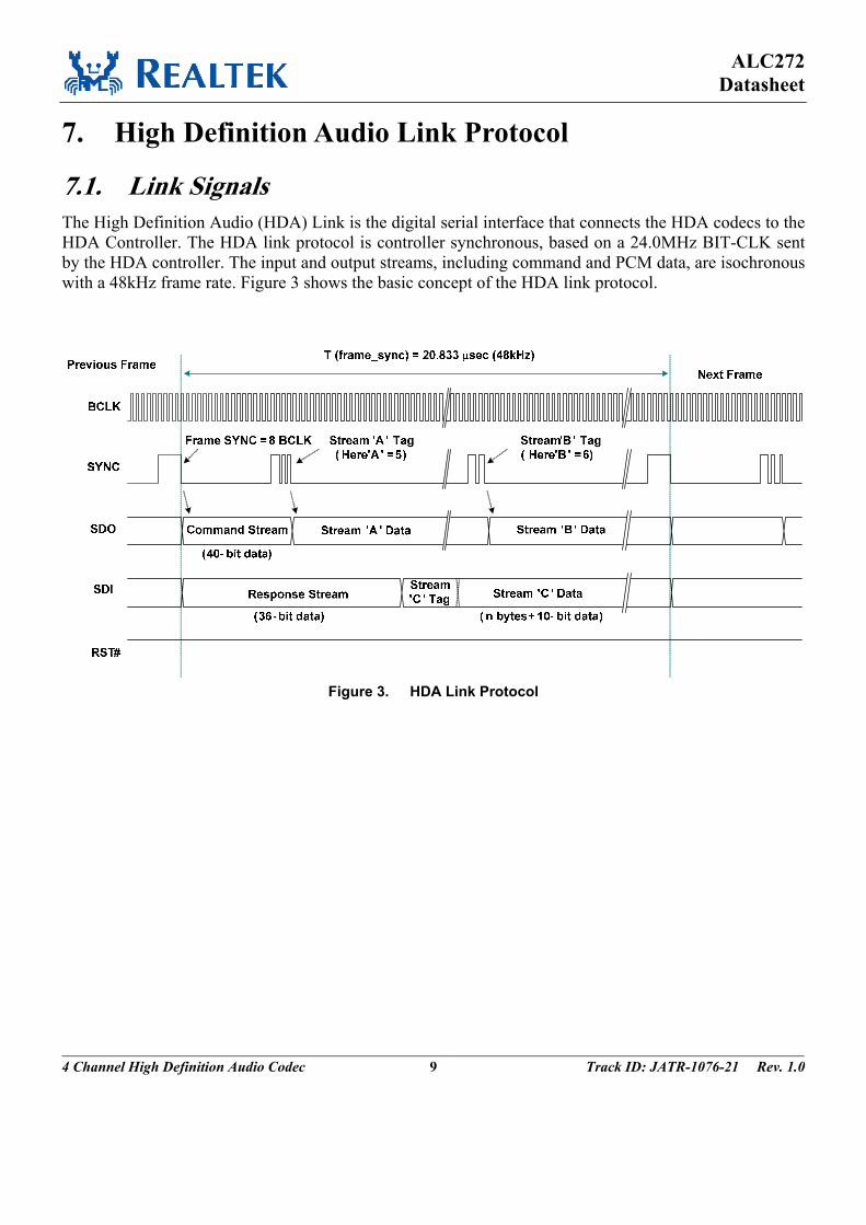
7. High Definition Audio Link Protocol
7.1. Link Signals The High Definition Audio (HDA) Link is the digital serial interface that connects the HDA codecs to the HDA Controller. The HDA link protocol is controller synchronous, based on a 24.0MHz BIT-CLK sent by the HDA controller. The input and output streams, including command and PCM data, are isochronous with a 48kHz frame rate. Figure 3 shows the basic concept of the HDA link protocol.
Figure 3. HDA Link Protocol

ALC272 Datasheet
4 Channel High Definition Audio Codec 10 Track ID: JATR-1076-21 Rev. 1.0
7.1.1. Signal Definitions Table 5. Link RESET#
Item Description BCLK 24.0MHz bit clock sourced from the HDA controller and connecting to all codecs. SYNC A 48kHz signal used to synchronize input and output streams on the link. It is sourced from the HDA
controller and connects to all codecs. SDO Serial Data Output signal driven by the HDA controller to all codecs. Commands and data streams are
carried on SDO. The data rate is double-pumped; the controller drives data onto the SDO, the codec samples data present on SDO with respect to each edge of BCLK. The HDA controller must support at least one SDO. To extend outbound bandwidth, multiple SDOs may be supported.
SDI Serial Data Input signal driven by the codec. This is point-to-point serial data from the codec to the HDA controller. The controller must support at least one SDI. Up to a maximum of 15 SDI’s can be supported. SDI is driven by the codec at each rising edge of BCLK, and sampled by the controller at each rising edge of BCLK. SDI can be driven by the controller to initialize the codec’s ID.
RESET# Active low reset signal. Asserted to reset the codec to default power-on state. RESET# is sourced from the HDA controller and connects to all codecs.
Table 6. HDA Signal Definitions Signal Name Source Type for Controller Description
BCLK Controller Output Global 24.0MHz bit clock. SYNC Controller Output Global 48kHz Frame Sync and outbound tag signal. SDO Controller Output Serial data output from controller. SDI Codec/Controller Input/Output Serial data input from codec. Weakly pulled down by the
controller. RESET# Controller Output Global active low reset signal.
SDO
SYNC
SDI
BCLK
Start of Frame
8-Bit Frame SYNC
7 6 5 4 0123 999 998 997 996 995 994 993 992 991 990
3 2 1 0 499 498 497 496 495 494
Controller samples SDI at rising edge of BCLK
Codec samples SDO at both rising and falling edge of BCLK
Figure 4. Bit Timing

ALC272 Datasheet
4 Channel High Definition Audio Codec 11 Track ID: JATR-1076-21 Rev. 1.0
7.1.2. Signaling Topology The HDA controller supports two SDOs for the outbound stream, up to 15 SDIs for the inbound stream. RESET#, BCLK, SYNC, SDO0, and SDO1 are driven by the controller to codecs. Each codec drives its own point-to-point SDI signal(s) to the controller.
Figure 5 shows the possible connections between the HDA controller and codecs:
• Codec 0 is a basic connection. There is one single SDO and one single SDI for normal transmission
• Codec 1 has two SDOs for doubled outbound rate, and a single SDI for normal inbound rate
• Codec 3 supports a single SDO for normal outbound rate, and two SDIs for doubled inbound rate
• Codec N has two SDOs and multiple SDIs
The multiple SDOs and multiple SDIs are used to expand the transmission rate between controller and codecs. Section 7.2 Frame Composition, page 12, describes the detailed outbound and inbound stream compositions for single and multiple SDOs/SDIs.
The connections shown in Figure 5 can be implemented concurrently in an HDA system. The ALC272 is designed to receive a single SDO stream.
RST#
BCLKSYN
CS
DO
0
SD
I0
Codec 0
RST#BCLKSYN
CS
DO
0S
DO
1S
DI0
Codec 1
RST#
BCLK
SYNC
SD
O0
SD
I1
Codec 2
HDAController
RST#BCLKSYNCSDO0SDO1SDI0
SDI2
SDI14
RST#BCLKSYN
CSD
O0
SDO
1
SDI1
Codec N
SD
I0
SD
I0
SDI1
SDI13
. . .
.
.
....
Single SDOSingle SDI
Two SDOsSingle SDI
Single SDOTwo SDIs
SDI2
Two SDOsMultiple SDIs
Figure 5. Signaling Topology

ALC272 Datasheet
4 Channel High Definition Audio Codec 12 Track ID: JATR-1076-21 Rev. 1.0
7.2. Frame Composition 7.2.1. Outbound Frame – Single SDO An outbound frame is composed of one 32-bit command stream and multiple data streams. There are one or multiple sample blocks in a data stream. Only one sample block exists in a stream if the HDA controller delivers a 48kHz rate of samples to the codec. Multiple sample blocks in a stream means the sample rate is a multiple of 48kHz. This means there should be 2 blocks in the same stream to carry 96kHz samples (Figure 6).
For outbound frames, the stream tag is not in SDO, but in the SYNC signal. A new data stream is started at the end of the stream tag. The stream tag includes a 4-bit preamble and 4-bit stream ID (Figure 7).
To keep the cadence of converters bound to the same stream, samples for these converters must be placed in the same block.
Command StreamSDO
SYNC
A 48kHz Frame is composed of Command stream and multiple Data streams
Stream 'X' DataStream 'A' Data
Stream 'A' Tag Stream 'X' TagFrame SYNC(Here 'A' = 5) (Here 'X' = 6)
Next FramePrevious Frame
0s
Null FieldSample Block(s)
Block 1 Block 2 ... Block Y
Sample 1 Sample 2 ... Sample Z
msb ... lsb
For 48kHz rate, only Block1 is included
One or multiple blocks in a stream
For 96kHz rate, Block1 includes (N)th time of samples, Block2includes (N+1)th time of samples
Z channels of PCM sample
msb first in a sample
Padded at theend of Frame
Figure 6. SDO Outbound Frame
SDO
SYNC
BCLK
Data of Stream 10
7 6 5 4 0123
Preamble Stream=10
1 1 00
msb lsb
msb
Previous Stream
Stream Tag
(4-Bit) (4-Bit)
Figure 7. SDO Stream Tag is Indicated in SYNC

ALC272 Datasheet
4 Channel High Definition Audio Codec 13 Track ID: JATR-1076-21 Rev. 1.0
7.2.2. Outbound Frame – Multiple SDOs The HDA controller allows two SDO signals to be used to stripe outbound data, completing transmission in less time to get more bandwidth. If software determines that the target codec supports multiple SDO capability, it enables the ‘Stripe Control’ bit in the controller’s Output Stream Control Register to initiate a specific stream (Stream ‘A’ in Figure 8) to be transmitted on multiple SDOs. In this case, the MSB of stream data is always carried on SDO0, the second bit on SDO1 and so forth.
SDO1 is for transmitting a striped stream. The codec does not support multiple SDOs connected to SDO0.
To guarantee all codecs can determine their corresponding stream, the command stream is not striped. It is always transmitted on SDO0, and copied on SDO1.
Figure 8. Striped Stream on Multiple SDOs

ALC272 Datasheet
4 Channel High Definition Audio Codec 14 Track ID: JATR-1076-21 Rev. 1.0
7.2.3. Inbound Frame – Single SDI An Inbound Frame – Single SDI is composed of one 36-bit response stream and multiple data streams. Except for the initialization sequence (turnaround and address frame), SDI is driven by the codec at each rising edge of BCLK. The controller also samples data at the rising edge of BCLK (Figure 9).
The SDI stream tag is not carried by SYNC, but included in the SDI. A complete SDI data stream includes one 4-bit stream tag, one 6-bit data length, and n-bit sample blocks. Zeros will be padded if the total length of the contiguous sample blocks within a given stream is not of integral byte length (Figure 10).
Response StreamSDI
SYNC
A 48kHz Frame is Composed of a Response Stream and Multiple Data streams
Stream 'X'Stream 'A'
Frame SYNC
Next FramePrevious Frame
0s
Null Field
Sample 1 Sample 2 ... Sample Z
msb ... lsb
For 48kHz rate, only Block1 is includedFor 96kHz rate, Block1, 2 includes (N) th (N+1)th time of samples
Z channels of PCM sample
msb first in a sample
Padded at the end of FrameSample Block(s)Stream Tag
Block 1 Block 2 ... Block Y Null Pad
Figure 9. SDI Inbound Stream
BCLK
SDI
Data Length in Bytes
Dn-1 0 0 0 0
Stream Tag
B0 Dn-2B1B2B3B4B5B6B7B8B9 D0
(Data Length in Bytes *8)-Bit
Next StreamNull Padn-Bit Sample Block
A Complete Stream Figure 10. SDI Stream Tag and Data

ALC272 Datasheet
4 Channel High Definition Audio Codec 15 Track ID: JATR-1076-21 Rev. 1.0
7.2.4. Inbound Frame – Multiple SDIs A codec can deliver data to the controller on multiple SDIs to achieve higher bandwidth. If an inbound stream exceeds the data transfer limits of a single SDI, the codec can divide the data onto separate SDI signals, each of which operate independently, with different stream numbers at the same frame time. This is similar to having multiple codecs connected to the controller. The controller samples the divided stream into separate memory with multiple DMA descriptors, then software re-combines the divided data into a meaningful stream.
Response StreamSDI0
SYNC
Stream 'X'
Frame SYNC
SDI1 0s
Tag A
Stream A, B, X, and Y are independent and have separate IDs
Data A
Tag B Data B
Codec drives SDI0 and SDI1
Stream 'A'
Stream 'B'
Response Stream 0s
Stream 'Y'
Figure 11. Codec Transmits Data Over Multiple SDIs
7.2.5. Variable Sample Rates The HDA link is designed for sample rates of 48kHz. Variable sample rates are delivered in multiple or sub-multiple rates of 48kHz. Two sample blocks per frame result in a 96kHz delivery rate, one sample block over two frames results in a 24kHz delivery rate. The HDA specification states that the sample rate of the outbound stream be synchronized by the controller, not by the codec. Each stream has its own sample rate, independent of any other stream.
The HDA controller supports 48kHz and 44.1kHz base rates. Table 7, page 16, shows the recommended sample rates based on multiples or sub-multiples of one of the two base rates.
Rates in sub-multiples (1/n) of 48kHz are interleaving n frames containing no sample blocks. Rates in multiples (n) of 48kHz contain n sample blocks in a frame. Table 8, page 16, shows the delivery cadence of variable rates based on 48kHz.
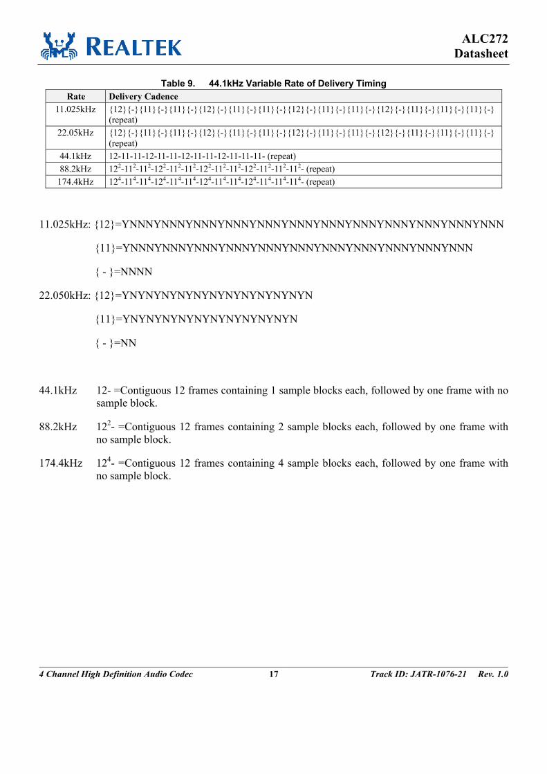
The HDA link is defined to operate at a fixed 48kHz frame rate. To deliver samples in (sub) multiple rates of 44.1kHz, an appropriate ratio between 44.1kHz and 48kHz must be maintained to avoid frequency drift. The appropriate ratio between 44.1kHz and 48kHz is 147/160. Meaning 147 sample blocks are transmitted every 160 frames.

ALC272 Datasheet
4 Channel High Definition Audio Codec 16 Track ID: JATR-1076-21 Rev. 1.0
The cadence ‘12-11-11-12-11-11-12-11-11-12-11-11-11- (repeat)’ interleaves 13 frames containing no sample blocks in every 160 frames. It provides a low long-term frequency drift for 44.1kHz of delivery rate. Rates in sub-multiples (1/n) of 44.1kHz also follow this cadence and interleave n empty frames. Rates in multiples (n) of 44.1kHz applying this cadence contain n sample blocks in the non-empty frame AND interleave an empty frame between non-empty frames (Table 9 , page 17).
Table 7. Defined Sample Rate and Transmission Rate (Sub) Multiple 48kHz Base 44.1kHz Base
1/6 8kHz (1 sample block every 6 frames) - 1/4 12kHz (1 sample block every 4 frames) 11.025kHz (1 sample block every 4 frames) 1/3 16kHz (1 sample block every 3 frames) - 1/2 - 22.05kHz (1 sample block every 2 frames) 2/3 32kHz (2 sample blocks every 3 frames) - 1 48kHz (1 sample block per frame) 44.1kHz (1 sample block per frame) 2 96kHz (2 sample blocks per frame) 88.2kHz (2 sample blocks per frame) 4 192kHz (4 sample blocks per frame) 176.4kHz (4 sample blocks per frame)
Table 8. 48kHz Variable Rate of Delivery Timing Rate Delivery Cadence Description 8kHz YNNNNN (repeat) One sample block is transmitted in every 6 frames 12kHz YNNN (repeat) One sample block is transmitted in every 4 frames 16kHz YNN (repeat) One sample block is transmitted in every 3 frames 32kHz Y2NN (repeat) One sample block is transmitted in every 6 frames 48kHz Y (repeat) One sample block is transmitted in each frames 96kHz Y2 (repeat) Two sample blocks are transmitted in each frame
192kHz Y4 (repeat) Four sample blocks are transmitted in each frame N: No sample block in a frame Y: One sample block in a frame Yx: X sample blocks in a frame
ALC272 Datasheet
4 Channel High Definition Audio Codec 17 Track ID: JATR-1076-21 Rev. 1.0
Table 9. 44.1kHz Variable Rate of Delivery Timing Rate Delivery Cadence
11.025kHz 12-11-11-12-11-11-12-11-11-12-11-11-11- (repeat)
22.05kHz 12-11-11-12-11-11-12-11-11-12-11-11-11- (repeat)
44.1kHz 12-11-11-12-11-11-12-11-11-12-11-11-11- (repeat) 88.2kHz 122-112-112-122-112-112-122-112-112-122-112-112-112- (repeat)
174.4kHz 124-114-114-124-114-114-124-114-114-124-114-114-114- (repeat)
11.025kHz: 12=YNNNYNNNYNNNYNNNYNNNYNNNYNNNYNNNYNNNYNNNYNNNYNNN
11=YNNNYNNNYNNNYNNNYNNNYNNNYNNNYNNNYNNNYNNNYNNN
- =NNNN
22.050kHz: 12=YNYNYNYNYNYNYNYNYNYNYNYN
11=YNYNYNYNYNYNYNYNYNYNYN
- =NN
44.1kHz 12- =Contiguous 12 frames containing 1 sample blocks each, followed by one frame with no sample block.
88.2kHz 122- =Contiguous 12 frames containing 2 sample blocks each, followed by one frame with no sample block.
174.4kHz 124- =Contiguous 12 frames containing 4 sample blocks each, followed by one frame with no sample block.

ALC272 Datasheet
4 Channel High Definition Audio Codec 18 Track ID: JATR-1076-21 Rev. 1.0
7.3. Reset and Initialization There are two types of reset within an HDA link:
• Link Reset Generated by assertion of the RESET# signal. All codecs return to their power-on state
• Codec Reset Generated by software directing a command to reset a specific codec back to its default state
An initialization sequence is requested after any of the following three events:
• Link Reset
• Codec Reset
• Codec changes its power state, e.g., hot docking a codec to an HDA system
7.3.1. Link Reset A link reset may be caused by any of the following three events:
1. The HDA controller asserts RESET# for any reason (power up, or PCI reset)
2. Software initiates a link reset via the ‘CRST’ bit in the Global Control Register (GCR) of the HDA controller
3. Software initiates power management sequences. Figure 12, page 19, shows the ‘Link Reset’ timing including the ‘Enter’ sequence (n~r) and ‘Exit’ sequence (s~v)
Enter ‘Link Reset’:
n Software writes a 0 to the ‘CRST’ bit in the Global Control Register of the HDA controller to initiate a link reset
o As the controller completes the current frame, it does not signal the normal 8-bit frame SYNC at the end of the frame
p The controller drives SYNC and all SDOs to low. Codecs also drive SDIs to low
q The controller asserts the RESET# signal to low, and enters the ‘Link Reset’ state
r All link signals driven by controller and codecs should be tri-state by internal pull-low resistors

ALC272 Datasheet
4 Channel High Definition Audio Codec 19 Track ID: JATR-1076-21 Rev. 1.0
Exit from ‘Link Reset’:
s If BCLK is re-started for any reason (codec, wake-up event, power management, etc.)
t Software is responsible for de-asserting RESET# after a minimum of 100µs BCLK running time (the 100µsec provides time for the codec PLL to stabilize)
u Minimum of 4 BCLKs after RESET# is de-asserted, the controller starts to signal normal frame SYNC
v The codec drives its SDI to request an initialization sequence (when the SDI is driven high at the last bit of frame SYNC)
SDOs
SYNC
SDIs
BCLK
Normal FrameSYNC is absent
RST#
4 BCLK 4 BCLK
Driven Low
Driven Low
Previous Frame
Normal FrameSYNC
Link in Reset
1
2
4 53 6 7
Pulled Low
Pulled Low
Driven Low Pulled Low
Pulled Low
8
9
>=100 usec >= 4 BCLK Initialization Sequence
Wake Event
Figure 12. Link Reset Timing
7.3.2. Codec Reset A ‘Codec Reset’ is initiated via the Codec RESET command verb. It results in the target codec being reset to the default state. After the target codec completes its reset operation, an initialization sequence is requested.
In the ALC272, the extend power state of conforming to Intel low power ECR the function reset could not initialize the register setting. Host SW needs to send “two” function reset consecutively to reset all settings.

ALC272 Datasheet
4 Channel High Definition Audio Codec 20 Track ID: JATR-1076-21 Rev. 1.0
7.3.3. Codec Initialization Sequence n The codec drives SDI high at the last bit of SYNC to request a Codec Address (CAD) from the controller
o The codec stops driving the SDI during this turnaround period
pqrs The controller drives SDI to assign a CAD to the codec
t The controller releases the SDI after the CAD has been assigned
u Normal operating state
SDIx
SYNC
BCLK
RST#
Connection Frame
1 2
4 5 6
7
Normal Operation
Response
Turnaround Frame Address Frame (Non-48kHz Frame)
Codec Drives SDIx
SD0 SD1 SD14
Controller Drives SDIx
Exit from Reset
Codec Turnaround(477 BCLK
Max.)
Frame SYNCFrame SYNCFrame SYNC
(Non-48kHz Frame)
Controller Turnaround( 477 BCLK
Max.)
3 8
Codec Drives SDIx
Figure 13. Codec Initialization Sequence
7.4. Verb and Response Format 7.4.1. Command Verb Format There are two types of verbs: one with 4-bit identifiers (4-bit verbs) and 16-bits of data, the other with 12-bit identifiers (12-bit verbs) and 8-bits of data. Table 10 shows the 4-bit verb structure of a command stream sent from the controller to operate the codec. Table 11 is the 12-bit verb structure that gets and controls parameters in the codec.
Table 10. 40-Bit Commands in 4-Bit Verb Format Bit [39:32] Bit [31:28] Bit [27:20] Bit [19:16] Bit [15:0] Reserved Codec Address Node ID Verb ID Payload
Table 11. 40-Bit Commands in 12-Bit Verb Format Bit [39:32] Bit [31:28] Bit [27:20] Bit [19:8] Bit [7:0] Reserved Codec Address Node ID Verb ID Payload

ALC272 Datasheet
4 Channel High Definition Audio Codec 21 Track ID: JATR-1076-21 Rev. 1.0
Table 12. Supported Commands
Supported Verb
Get
Ver
b
Set V
erb
Roo
t Nod
e
Aud
io F
unct
ion
Gro
up
Mod
em F
unct
ion
Gro
up*1
HD
MI F
unct
ion
Gro
up*1
Vend
or D
efin
e G
roup
*1
Aud
io O
ut C
onve
rter
Aud
io In
Con
vert
er
Pin
Wid
get
Sum
Wid
get
Sele
ctor
Wid
get
Pow
er W
idge
t*1
Volu
me
Kno
b
Bee
p G
ener
ator
Vend
or D
efin
ed W
idge
t
Get parameter F00 - Y Y - - - Y Y Y Y Y Y Y Y Y Connection Select F01 701 - - - - - - Y Y - Y - - - - Get Connection List Entry F02 - - - - - - - Y Y Y Y - - - - Processing State F03 703 - - - - - - - - - - - - - - Coefficient Index D-- 5-- - - - - - - - - - - - - - Y Processing Coefficient C-- 4-- - - - - - - - - - - - - - Y Amplifier Gain/Mute B-- 3-- - - - - - - Y Y Y - - - - - Stream Format A-- 2-- - - - - - Y Y - - - - - - - Digital Converter 1 F0D 70D - - - - - Y Y - - - - - - - Digital Converter 2 F0D 70E - - - - - Y Y - - - - - - - Power State F05 705 - Y - - - Y Y Y - - - - - - Channel / Stream ID F06 706 - - - - Y Y - - - - - - - SDI Select F04 704 - - - - - - - - - - - - - - Pin Widget Control F07 707 - - - - - - - Y - - - - - - Unsolicited Enable F08 708 - - - - - - - Y - - - Y - - Pin Sense F09 709 - - - - - - - Y - - - - - - EAPD Control F0C 70C - - - - - - - Y - - - - - - All GPIO Control F10-
F1A 710- 71A
- Y - - - - - - - - - - - -
Beep Generator Control F0A 70A - - - - - - - - - - - - Y - Volume Knob Control F0F 70F - - - - - - - - - - - - - - Subsystem ID, Byte 0 F20 720 - Y - - - - - - - - - - - - Subsystem ID, Byte 1 F20 721 - Y - - - - - - - - - - - - Subsystem ID, Byte 2 F20 722 - Y - - - - - - - - - - - - Subsystem ID, Byte 3 F20 723 - Y - - - - - - - - - - - - Config Default, Byte 0 F1C 71C - - - - - - - Y - - - - - - Config Default, Byte 1 F1C 71D - - - - - - - Y - - - - - - Config Default, Byte 2 F1C 71E - - - - - - - Y - - - - - - Config Default, Byte 3 F1C 71F - - - - - - - Y - - - - - - RESET - 7FF - Y - - - - - - - - - - - - *1: The ALC272 does not support Modem/HDMI/Vendor groups and Power State widgets.

ALC272 Datasheet
4 Channel High Definition Audio Codec 22 Track ID: JATR-1076-21 Rev. 1.0
Table 13. Supported Parameters
Supported Parameter
Para
met
er ID
Roo
t Nod
e
Aud
io F
unct
ion
Gro
up
Mod
em F
unct
ion
Gro
up*1
HD
MI F
unct
ion
Gro
up*1
Vend
or D
efin
e G
roup
*1
Aud
io O
ut C
onve
rter
Aud
io In
Con
vert
er
Pin
Wid
get
Sum
Wid
get
Sele
ctor
Wid
get
Pow
er W
idge
t*1
Volu
me
Kno
b
Bee
p G
ener
ator
Vend
or D
efin
ed W
idge
t
Vendor ID 00 Y - - - - - - - - - - - - - Revision ID 02 Y - - - - - - - - - - - - - Subordinate Node Count 04 Y Y - - - - - - - - - - - - Function Group Type 05 - Y - - - - - - - - - - - - Audio Function Group Capabilities
08 - Y - - - - - - - - - - - -
Audio Widget Capabilities 09 - - - - - Y Y Y Y Y Y Y Y Y Sample Size, Rate 0A - Y - - - Y Y - - - - - - - Stream Formats 0B - Y - - - Y Y - - - - - - - Pin Capabilities 0C - - - - - - - Y - - - - - - Input Amp Capabilities 0D - - - - - - Y - Y Y - - - - Output Amp Capabilities 12 - - - - - - - Y Y - - - - - Connection List Length 0E - - - - - - Y Y Y Y - - - - Supported Power States 0F - Y - - - Y Y Y Y Y - - - Y Processing Capabilities 10 - - - - - - - - - - - - - Y GPI/O Count 11 - - - - - - - - - - - - - - Volume Knob Capabilities 13 - - - - - - - - - - - - - - *1: The ALC272 does not support Modem/HDMI/Vendor groups and Power State widgets.

ALC272 Datasheet
4 Channel High Definition Audio Codec 23 Track ID: JATR-1076-21 Rev. 1.0
7.4.2. Response Format There are two types of response from the codec to the controller. Solicited Responses are returned by the codec in response to a current command verb. The codec will send Solicited Response data in the next frame, without regard to the Set (Write) or Get (Read) command. The 32-bit response is interpreted by software, opaque to the controller.
Unsolicited Responses are sent by the codec independently of software requests. Jack Detection or GPI status information can be actively delivered to the controller and interpreted by software. The ‘Tag’ in Bit[31:28] is used to identify unsolicited events. This tag is undefined in the HDA specifications.
Table 14. Solicited Response Format Bit [35] Bit [34] Bit [33:32] Bit [31:0] Valid Unsol=0 Reserved Response
Table 15. Unsolicited Response Format Bit [35] Bit [34] Bit [33:32] Bit [31:28] Bit [27:0] Valid Unsol=1 Reserved Tag Response
7.4.3. Double Function Reset This new reset is created by sending two Function Group resets back to back. This Function Group ‘Double’ reset shall do a full initialization and reset all settings to their power on defaults. A Double reset is defined as two Function Group Reset verbs received without any other intervening valid verbs. The reset verbs are not required to be received in sequential frames, but there must not be any other verbs received in frames between the receipt of the Function Group Reset verbs. It is allowed that there are several null commands received in frames between Function Group Reset verbs.

ALC272 Datasheet
4 Channel High Definition Audio Codec 24 Track ID: JATR-1076-21 Rev. 1.0
7.5. Power Management The ALC272 is designed to meet Intel’s low-power-state white paper and is ECR HDA-015B compliant. It meets the five attributes discussed in the white paper:
1. D3 state power < 30mW (without PC-Beep pass-through Function, with PC-Beep pass-through Function, the criteria is 60mW.
2. Exit latency (D3 to D0 transfer) < 10ms.
3. Audio pop/click suppression during D3 and D0 transition < -65dBV.
4. Supports Jack detection in D3 state.
5. D3 functions with or without the BITCLK
The ALC272 minimizes D3 state idle mode power consumption and increases overall battery life in mobile systems.
In D3 mode, only a power on reset or a ‘double function reset’ resets all ALC272 settings, cutting software configuration time spent entering/leaving D3 state, and reducing latency time for D3 to D0 transitions.
The ALC272 supports Wake-Up events in D3 mode, including jack detection and GPIO status changes. If the HDA-Link was alive (with BCLK), the ALC272 Wake-Up response is as normal. If no BITCLK is present, the ALC272 drives the SDI high in order to wake up the system
Figure 14. Resume From External Event (Wake-Up Event)

ALC272 Datasheet
4 Channel High Definition Audio Codec 25 Track ID: JATR-1076-21 Rev. 1.0
All power management state changes in widgets are driven by software. Table 16 shows the System Power State Definitions.
In the ALC272, all the widgets, including output/input converters, support power control. Software may have various power states depending on system configuration. Table 17 indicates those nodes that support power management. To simplify power control, software can configure whole codec power states through the audio function (NID=01h). Output converters (DACs) and input converters (ADCs) have no individual power control to supply fine-grained power control.
Table 16. System Power State Definitions Power States Definitions
D0 All power on. Individual DACs and ADCs can be powered up or down as required. D1 All amplifiers and converters (DACs and ADCs) are powered down. State maintained, analog
reference stays up. D2 All amplifiers and converters (DACs and ADCs) are powered down. State maintained, but analog
reference is off (D1 + analog reference off). D3 Power still supplied. The codec stops the internal clock. State is maintained.
D3 (No BitCLK) Power still supplied, BITCLK stopped, and Reset in low state.
Table 17. Power Controls in NID 01h Description D0 D1 D2 D3 D3 (No bclk) Link Reset
LINK Response Normal Normal Normal PD PD PD DACs Normal PD PD PD PD PD ADCs Normal PD PD PD PD PD All Headphone Drivers Normal Normal PD PD PD Normal All Mixers Normal Normal PD PD PD Normal
Audio Function (NID=01h)
All Reference Normal Normal PD PD PD Normal
Table 18. Powered Down Conditions Condition Description LINK Response powered down Internal clock is stopped. SDATA-IN and SPDIF-OUT are floated with pulled
low 47K resistors internally. SPDIF-IN is also floated. Detection of ‘Link Reset Entry’ and ‘Link Reset Exit’ sequences are supported. All states are maintained if DVDD is supplied.
DACs powered down Analog block and digital filter are powered down. ADCs powered down Analog block and digital filter are powered down. Data on SDATA-IN is quiet. Headphone Driver powered down All headphone drivers are powered down. Mixers powered down All internal mixer widgets are powered down. The DC reference and
VREFOUTx at individual pin complexes are still alive. Reference power down All internal references, DC reference, and VREFOUTx at individual pin
complexes are off.

ALC272 Datasheet
4 Channel High Definition Audio Codec 26 Track ID: JATR-1076-21 Rev. 1.0
8. Supported Verbs and Parameters This section describes the Verbs and Parameters supported by various widgets in the ALC272. If a verb is not supported by the addressed widget, it will respond with 32 bits of ‘0’.
8.1. Verb – Get Parameters (Verb ID=F00h) The ‘Get Parameters’ verb is used to get system information and the function capabilities of the HDA codec. All the parameters are read-only. There are a total of 15 ID parameters defined for each widget. Some parameters are supported only in a specific widget. Refer to section 7.4.1 Command Verb Format, page 20, to get detailed information about supported parameters.
Table 19. Verb – Get Parameters (Verb ID=F00h) Get Parameter Command Format Codec Response Format Bit [31:28] Bit [27:20] Bit [19:8] Payload Bit [7:0] Response [31:0]
CAd=X Node ID=00h Verb ID=F00h Parameter ID[7:0] 32-bit Response Note: If the parameter ID is not supported, the returned response is 32 bits of ‘0’.
8.1.1. Parameter – Vendor ID (Verb ID=F00h, Parameter ID=00h) Table 20. Parameter – Vendor ID (Verb ID=F00h, Parameter ID=00h)
Codec Response Format Bit Description
31:16 Vendor ID=10ECh (Realtek’s PCI vendor ID). 15:0 Device ID=0272h.
Note 1: The Root Node (NID=00h) supports this parameter.
8.1.2. Parameter – Revision ID (Verb ID=F00h, Parameter ID=02h) Table 21. Parameter – Revision ID (Verb ID=F00h, Parameter ID=02h)
Codec Response Format Bit Description
31:24 Reserved. Read as 0’s. 23:20 MajRev=1h. The major version number (in decimal) of the HDA Specification to which the ALC272 is
fully compliant. 19:16 MinRev=0h. The minor version number (in decimal) of the HDA Specification to which the ALC272 is
fully compliant. 15:8 Revision ID. The vendor’s revision number.
Note: 00h indicates ALC272 silicon. 7:0 Stepping ID. The vendor’s stepping number within the given Revision ID.
Note: The Root Node (NID=00h) supports this parameter.

ALC272 Datasheet
4 Channel High Definition Audio Codec 27 Track ID: JATR-1076-21 Rev. 1.0
8.1.3. Parameter – Subordinate Node Count (Verb ID=F00h, Parameter ID=04h)
For the root node, the Subordinate Node Count provides information about audio function group nodes associated with the root node.
For function group nodes, it provides the total number of widgets associated with this function node.
Table 22. Parameter – Subordinate Node Count (Verb ID=F00h, Parameter ID=04h) Codec Response Format
Bit Description 31:24 Reserved. Read as 0’s. 23:16 Starting Node Number. The starting node number in the sequential widgets 15:8 Reserved. Read as 0’s. 7:0 Total Number of Nodes. For a root node, this is the total number of function groups in the root node.
For a function group, this is the total number of widget nodes in the function group.
8.1.4. Parameter – Function Group Type (Verb ID=F00h, Parameter ID=05h) Table 23. Parameter – Function Group Type (Verb ID=F00h, Parameter ID=05h)
Codec Response Format Bit Description
31:9 Reserved. Read as 0’s. 8 UnSol Capable.
0: Unsolicited response is not supported by this function group. 1: Unsolicited response is supported by this function group.
7:0 Function Group Type. 00h: Reserved 01h: Audio Function 02h: Modem Function 03h~7Fh: Reserved 80h~FFh: Vendor Defined Function
8.1.5. Parameter– Audio Function Capabilities (Verb ID=F00h, Parameter ID=08h)
Table 24. Parameter – Audio Function Capabilities (Verb ID=F00h, Parameter ID=08h) Codec Response Format
Bit Description 31:17 Reserved. Read as 0’s.
16 Beep Generator. A ‘1’ indicates the presence of an integrated Beep generator within the Audio Function Group.
15:12 Reserved. Read as 0’s. 11:8 Input Delay. Number of samples delay from analog input to HDA link. 7:4 Reserved. Read as 0’s. 3:0 Output Delay. Number of samples delay from HDA link to analog output.

ALC272 Datasheet
4 Channel High Definition Audio Codec 28 Track ID: JATR-1076-21 Rev. 1.0
8.1.6. Parameter – Audio Widget Capabilities (Verb ID=F00h, Parameter ID=09h)
Table 25. Parameter – Audio Widget Capabilities (Verb ID=F00h, Parameter ID=09h) Codec Response Format
Bit Description 31:24 Reserved. Read as 0’s. 23:20 Widget Type.
0h: Audio Output 1h: Audio Input 2h: Mixer 3h: Selector 4h: Pin Complex 5h: Power Widget 6h: Volume Knob Widget 7h~Eh: Reserved Fh: Vendor defined audio widget
19:16 Delay. Samples delayed between the HDA link and widgets. 15:12 Reserved. Read as 0’s.
11: L-R Swap. 0: Left channel and right channel swapping is not supported 1: Left channel and right channel swapping is supported
10 Power Control. 0: Power control is not supported on this widget 1: Power control is supported on this widget
9 Digital. 0: An analog input or output converter 1: A widget translating digital data between the HDA link and digital I/O (SPDIF, I2S, etc.)
8 ConnList. Connection List. 0: Connected to HDA link. No Connection List Entry will be queried 1: Connection List Entry must be queried
7 UnsolCap. Unsolicited Capable. 0: Unsolicited response is not supported 1: Unsolicited response is supported
6 ProcWidget. Processing Widget. 0: No processing control 1: Processing control is supported
5 Reserved. Read as 0. 4 Format Override.
Note: The ALC272 supports 16/20/24-bit with 44.1kHz, 48kHz, 96kHz and 192kHz sample rate. The format (parameter ID=0Ah) must be queried
3 AmpParOvr (AMP Param Override). Override amplifier parameters (Gain Control) in individual output Pin Complexes, ADCs, and Mixer widgets.
2 OutAmpPre (Out AMP Present). 1 InAmpPre (In AMP Present).
There are amplifiers (Gain Control) in individual ADCs and Mixer widgets. 0 Stereo.
0: Mono Widget 1: Stereo Widget
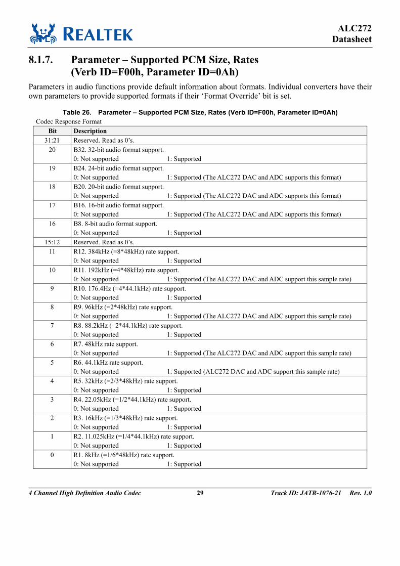
ALC272 Datasheet
4 Channel High Definition Audio Codec 29 Track ID: JATR-1076-21 Rev. 1.0
8.1.7. Parameter – Supported PCM Size, Rates (Verb ID=F00h, Parameter ID=0Ah)
Parameters in audio functions provide default information about formats. Individual converters have their own parameters to provide supported formats if their ‘Format Override’ bit is set.
Table 26. Parameter – Supported PCM Size, Rates (Verb ID=F00h, Parameter ID=0Ah) Codec Response Format
Bit Description 31:21 Reserved. Read as 0’s.
20 B32. 32-bit audio format support. 0: Not supported 1: Supported
19 B24. 24-bit audio format support. 0: Not supported 1: Supported (The ALC272 DAC and ADC supports this format)
18 B20. 20-bit audio format support. 0: Not supported 1: Supported (The ALC272 DAC and ADC supports this format)
17 B16. 16-bit audio format support. 0: Not supported 1: Supported (The ALC272 DAC and ADC supports this format)
16 B8. 8-bit audio format support. 0: Not supported 1: Supported
15:12 Reserved. Read as 0’s. 11 R12. 384kHz (=8*48kHz) rate support.
0: Not supported 1: Supported 10 R11. 192kHz (=4*48kHz) rate support.
0: Not supported 1: Supported (The ALC272 DAC and ADC support this sample rate) 9 R10. 176.4Hz (=4*44.1kHz) rate support.
0: Not supported 1: Supported 8 R9. 96kHz (=2*48kHz) rate support.
0: Not supported 1: Supported (The ALC272 DAC and ADC support this sample rate) 7 R8. 88.2kHz (=2*44.1kHz) rate support.
0: Not supported 1: Supported 6 R7. 48kHz rate support.
0: Not supported 1: Supported (The ALC272 DAC and ADC support this sample rate) 5 R6. 44.1kHz rate support.
0: Not supported 1: Supported (ALC272 DAC and ADC support this sample rate) 4 R5. 32kHz (=2/3*48kHz) rate support.
0: Not supported 1: Supported 3 R4. 22.05kHz (=1/2*44.1kHz) rate support.
0: Not supported 1: Supported 2 R3. 16kHz (=1/3*48kHz) rate support.
0: Not supported 1: Supported 1 R2. 11.025kHz (=1/4*44.1kHz) rate support.
0: Not supported 1: Supported 0 R1. 8kHz (=1/6*48kHz) rate support.
0: Not supported 1: Supported

ALC272 Datasheet
4 Channel High Definition Audio Codec 30 Track ID: JATR-1076-21 Rev. 1.0
8.1.8. Parameter – Supported Stream Formats (Verb ID=F00h, Parameter ID=0Bh)
Parameters in this node only provide default information for audio function groups. Individual converters have their own parameters to provide supported formats if the ‘Format Override’ bit is set.
Table 27. Parameter – Supported Stream Formats (Verb ID=F00h, Parameter ID=0Bh) Codec Response Format
Bit Description 31:3 Reserved. Read as 0’s.
2 AC3. 0: Not supported 1: Supported
1 Float32. 0: Not supported 1: Supported
0 PCM. 0: Not supported 1: Supported (The ALC272 DAC and ADC support this format)
Note: Input converters and output converters support this parameter.
8.1.9. Parameter – Pin Capabilities (Verb ID=F00h, Parameter ID=0Ch)
The Pin Capabilities parameter returns a bit field describing the capabilities of the Pin Complex widget.
Table 28. Parameter – Pin Capabilities (Verb ID=F00h, Parameter ID=0Ch) Codec Response Format
Bit Description 31:16 Reserved. Read as 0’s. 15:8 VREF Control Capability. ‘1’ in corresponding bit field indicates signal levels of associated Vrefout are
specified as a percentage of AVDD. 7:6 5 4 3 2 1 0
Reserved 100% 80% Reserved Ground 50% Hi-Z
7 Reserved. 6 Balanced I/O Pin. ‘1’ indicates this pin complex has balanced pins. 5 Input Capable. ‘1’ indicates this pin complex supports input. 4 Output Capable. ‘1’ indicates this pin complex supports output. 3 Headphone Drive Capable. ‘1’ indicates this pin complex has an amplifier to drive a headphone. 2 Presence Detect Capable. ‘1’ indicates this pin complex can detect whether there is a device plugged in. 1 Trigger Required. ‘1’ indicates whether a software trigger is required for an impedance measurement. 0 Impedance Sense Capable.
‘1’ indicates this pin complex can perform analog sense on the attached device to determine its type. Note: Only Pin Complex widgets support this parameter.

ALC272 Datasheet
4 Channel High Definition Audio Codec 31 Track ID: JATR-1076-21 Rev. 1.0
8.1.10. Parameter– Amplifier Capabilities (Verb ID=F00h, Input Amplifier Parameter ID=0Dh)
Parameters in this node provide audio function group default information. Individual converters have their own parameters to provide amplifier capabilities if the ‘AMP Param Override’ bit is set.
Table 29. Parameter – Amplifier Capabilities (Verb ID=F00h, Input Amplifier Parameter ID=0Dh) Codec Response Format
Bit Description 31 (Input) Mute Capable.
30:23 Reserved. Read as 0. 22:16 Step Size.
Indicates the size of each step in the gain range. 15 Reserved. Read as 0.
14:8 Number of Steps. Indicates the number of steps in the gain range. ‘0’ means the gain is fixed.
7 Reserved. Read as 0. 6:0 Offset.
Indicates which step is 0dB.
8.1.11. Parameter – Amplifier Capabilities (Verb ID=F00h, Output Amplifier Parameter ID=12h)
Parameters in this node provide audio function group default information. Individual converters have their own parameters to provide amplifier capabilities if the ‘AMP Param Override’ bit is set.
Table 30. Parameter – Amplifier Capabilities (Verb ID=F00h, Output Amplifier Parameter ID=12h) Codec Response Format
Bit Description 31 (Output) Mute Capable.
30:23 Reserved. Read as 0. 22:16 Step Size.
Indicates the size of each step in the gain range. Each individual step may be 0~32dB, specified in 0.25dB steps. ‘0’ indicates 0.25dB steps. ‘127’ indicates 32dB steps.
15 Reserved. Read as 0. 14:8 Number of Steps.
Indicates the number of steps in the gain range. ‘0’ means the gain is fixed. 7 Reserved. Read as 0.
6:0 Offset. Indicates which step is 0dB.

ALC272 Datasheet
4 Channel High Definition Audio Codec 32 Track ID: JATR-1076-21 Rev. 1.0
8.1.12. Parameter – Connect List Length (Verb ID=F00h, Parameter ID=0Eh)
Parameters in this node provide audio function widget connection information.
Table 31. Parameter – Connect List Length (Verb ID=F00h, Parameter ID=0Eh) Codec Response Format
Bit Description 31:8 Reserved. Read as 0.
7 Short Form. 0: Short Form 1: Long Form
6:0 Connect List Length. Indicates the number of inputs connected to a widget. If the Connect List Length is 1, there is only one input, and there is no Connection Select Control (not a MUX widget).
8.1.13. Parameter – Supported Power States (Verb ID=F00h, Parameter ID=0Fh)
Table 32. Parameter – Supported Power States (Verb ID=F00h, Parameter ID=0Fh) Codec Response Format
Bit Description 31 Extended Power States Supported (EPSS).
1: Extended power state EPSS is supported 30 CLKSTOP.
1: D3 mode operates even when no BITCLK presents on the link 29:4 Reserved. Read as 0’s.
3 D3Sup. 1: Power state D3 is supported
2 D2Sup 1: Power state D2 is supported
1 D1Sup 1: Power state D1 is supported
0 D0Sup 1: Power state D0 is supported

ALC272 Datasheet
4 Channel High Definition Audio Codec 33 Track ID: JATR-1076-21 Rev. 1.0
8.1.14. Parameter – Processing Capabilities (Verb ID=F00h, Parameter ID=10h) Table 33. Parameter – Processing Capabilities (Verb ID=F00h, Parameter ID=10h)
Codec Response Format Bit Description
31:16 Reserved. Read as 0’s. 15:8 NumCoeff. Number of Coefficient. 7:1 Reserved. Read as 0’s. 0 Benign.
0: Processing unit is not linear and time invariant 1: Processing unit is linear and time invariant
8.1.15. Parameter – GPIO Capabilities (Verb ID=F00h, Parameter ID=11h)
Table 34. Parameter – GPIO Capabilities (Verb ID=F00h, Parameter ID=11h) Codec Response Format
Bit Description 31 GPIWake=0. The ALC272 does not support GPIO wake-up function. 30 GPIUnsol=1. The ALC272 supports GPIO unsolicited response.
29:24 Reserved. Read as 0’s. 23:16 NumGPIs=00h. No GPI pin is supported. 15:8 NumGPOs=00h. No GPO pin is supported. 7:0 NumGPIOs=02h. Two GPIO pins are supported.
8.1.16. Parameter – Volume Knob Capabilities (Verb ID=F00h, Parameter ID=13h)
Table 35. Parameter – Volume Knob Capabilities (Verb ID=F00h, Parameter ID=13h) Codec Response Format for NID=21h (Volume Control Knob)
Bit Description 31:8 Reserved. Read as 0’s.
7 Delta. 0: Software cannot modify the Volume Control Knob volume 1: Software can write a base volume to the Volume Control Knob
6:0 NumSteps. The number of steps in the range of the Volume Control Knob.
Note: The ALC272 does not support volume knob and will respond with 0s to this parameter.

ALC272 Datasheet
4 Channel High Definition Audio Codec 34 Track ID: JATR-1076-21 Rev. 1.0
8.2. Verb – Get Connection Select Control (Verb ID=F01h) Table 36. Verb – Get Connection Select Control (Verb ID=F01h)
Get Command Format Codec Response Format Bit [31:28] Bit [27:20] Bit [19:8] Payload Bit [7:0] Response [31:0]
CAd=X Node ID=Xh Verb ID=F01h 0’s Bit[7:0] are Connection Index
Codec Response for NID = 14h (LOUT1, PORT-D) Bit Description
31:8 0’s. 7:0 Connection Index Currently Set (Default value is 00h).
00h: Sum Widget NID=0Ch 01h: Sum Widget NID=0Dh Other: Reserved
Codec Response for NID = 15h (LOUT2, PORT-A)
Bit Description 31:8 0’s. 7:0 Connection Index Currently Set (Default value is 00h).
00h: Sum Widget NID=0Ch 01h: Sum Widget NID=0Dh Other: Reserved
Codec Response for NID = 19h (MIC2, PORT-F)
Bit Description 31:8 0’s. 7:0 Connection Index Currently Set (Default value is 00h).
00h: Sum Widget NID=0Ch 01h: Sum Widget NID=0Dh 02h: Sum Widget NID=0Eh Other: Reserved
Codec Response for NID = 1Bh (LINE2, PORT-E)
Bit Description 31:8 0’s. 7:0 Connection Index Currently Set (Default value is 00h).
00h: Sum Widget NID=0Ch 01h: Sum Widget NID=0Dh 02h: Sum Widget NID=0Eh Other: Reserved
Codec Response for NID = 21h (HP-OUT, PORT-I)
Bit Description 31:8 0’s. 7:0 Connection Index Currently Set (Default value is 00h).
00h: Sum Widget NID=0Ch 01h: Sum Widget NID=0Dh 02h: Sum Widget NID=0Eh Other: Reserved
Codec Response for other NID
Bit Description 31:0 Not Supported (returns 00000000h).

ALC272 Datasheet
4 Channel High Definition Audio Codec 35 Track ID: JATR-1076-21 Rev. 1.0
8.3. Verb – Set Connection Select (Verb ID=701h) Table 37. Verb – Set Connection Select (Verb ID=701h)
Set Command Format Codec Response Format Bit [31:28] Bit [27:20] Bit [19:8] Payload Bit [7:0] Response [31:0]
CAd=X Node ID=Xh Verb ID=701h Select Index [7:0] 0’s for all nodes
8.4. Verb – Get Connection List Entry (Verb ID=F02h) Table 38. Verb – Get Connection List Entry (Verb ID=F02h)
Get Command Format Codec Response Format Bit [31:28] Bit [27:20] Bit [19:8] Payload Bit [7:0] Response [31:0]
CAd=X Node ID=Xh Verb ID=F02h Offset Index - N[7:0] 32-bit Response
Codec Response for NID=08h (ADC) Bit Description
31:8 Connection List Entry (N+3), (N+2), and (N+1). Returns 000000h.
7:0 Connection List Entry (N). Returns 23h (Sum Widget) for N=0~3. Returns 00h for N>3.
Codec Response for NID=09h (ADC)
Bit Description 31:8 Connection List Entry (N+3), (N+2), and (N+1).
Returns 000000h. 7:0 Connection List Entry (N).
Returns 22h (Sum Widget) for N=0~3. Returns 00h for N>3.
Codec Response for NID=0Bh (Mixer)
Bit Description 31:24 Connection List Entry (N+3).
Return 1Bh (Pin Complex – LINE2) for N=0~3. Return 00h for N>7.
23:16 Connection List Entry (N+2). Return 1Ah (Pin Complex – LINE1) for N=0~3. Return 15h (Pin Complex – LOUT2) for N=4~7. Return 00h for N>7.
15:8 Connection List Entry (N+1). Return 19h (Pin Complex – MIC2) for N=0~3. Return 14h (Pin Complex –LOUT1) for N=4~7. Return 00h for N>7.
7:0 Connection List Entry (N). Return 18h (Pin Complex – MIC1) for N=0~3. Return 1Dh (Pin Complex –PCBEEP) for N=4~7. Return 00h for N>7.
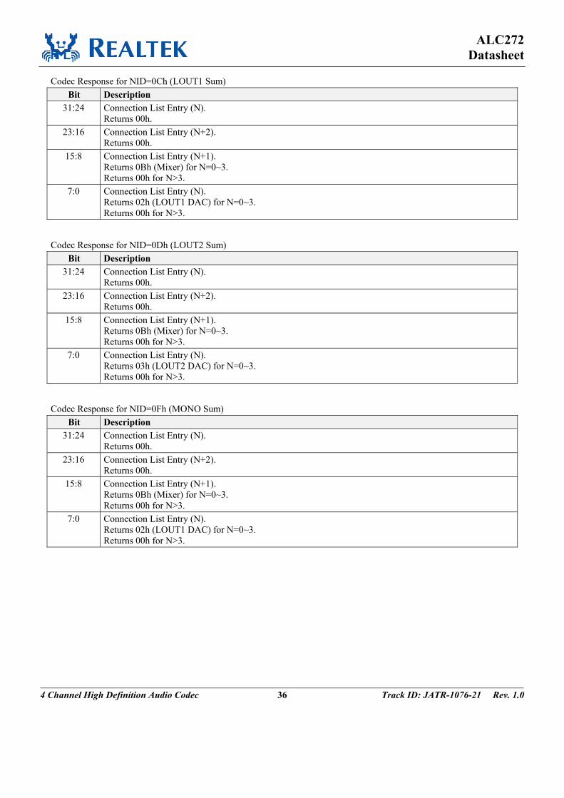
ALC272 Datasheet
4 Channel High Definition Audio Codec 36 Track ID: JATR-1076-21 Rev. 1.0
Codec Response for NID=0Ch (LOUT1 Sum) Bit Description
31:24 Connection List Entry (N). Returns 00h.
23:16 Connection List Entry (N+2). Returns 00h.
15:8 Connection List Entry (N+1). Returns 0Bh (Mixer) for N=0~3. Returns 00h for N>3.
7:0 Connection List Entry (N). Returns 02h (LOUT1 DAC) for N=0~3. Returns 00h for N>3.
Codec Response for NID=0Dh (LOUT2 Sum)
Bit Description 31:24 Connection List Entry (N).
Returns 00h. 23:16 Connection List Entry (N+2).
Returns 00h. 15:8 Connection List Entry (N+1).
Returns 0Bh (Mixer) for N=0~3. Returns 00h for N>3.
7:0 Connection List Entry (N). Returns 03h (LOUT2 DAC) for N=0~3. Returns 00h for N>3.
Codec Response for NID=0Fh (MONO Sum)
Bit Description 31:24 Connection List Entry (N).
Returns 00h. 23:16 Connection List Entry (N+2).
Returns 00h. 15:8 Connection List Entry (N+1).
Returns 0Bh (Mixer) for N=0~3. Returns 00h for N>3.
7:0 Connection List Entry (N). Returns 02h (LOUT1 DAC) for N=0~3. Returns 00h for N>3.

ALC272 Datasheet
4 Channel High Definition Audio Codec 37 Track ID: JATR-1076-21 Rev. 1.0
Codec Response for NID=14h (LOUT1, Port-D) Bit Description
31:24 Connection List Entry (N+3). Return 00h.
23:16 Connection List Entry (N+2). Return 00h.
15:8 Connection List Entry (N+1). Return 0Dh (Sum Widget NID=0Dh) for N=0~3. Return 00h.
7:0 Connection List Entry (N). Return 0Ch (Sum Widget NID=0Ch) for N=0~3. Return 00h for N>3.
Codec Response for NID=15h (LOUT2, Port-A)
Bit Description 31:24 Connection List Entry (N+3).
Return 00h. 23:16 Connection List Entry (N+2).
Return 00h. 15:8 Connection List Entry (N+1).
Return 0Dh (Sum Widget NID=0Dh) for N=0~3. Return 00h.
7:0 Connection List Entry (N). Return 0Ch (Sum Widget NID=0Ch) for N=0~3. Return 00h for N>3.
Codec Response for NID=17h (MONO, Port-H)
Bit Description 31:8 Connection List Entry (N+3), (N+2), (N+1).
Returns 000000h for n>3. 7:0 Connection List Entry (N).
Returns 0Fh (Sum Widget NID=0Fh) for N=0~3. Returns 00h for N>3.
Codec Response for NID=18h (MIC1, Port-B)
Bit Description 31:8 Connection List Entry (N+3), (N+2), (N+1).
Returns 000000h for n>3. 7:0 Connection List Entry (N).
Returns 00h for N>3.

ALC272 Datasheet
4 Channel High Definition Audio Codec 38 Track ID: JATR-1076-21 Rev. 1.0
Codec Response for NID=19h (MIC2, Port-F) Bit Description
31:24 Connection List Entry (N+3). Return 00h.
23:16 Connection List Entry (N+2). Return 00h for N>3.
15:8 Connection List Entry (N+1). Return 0Dh (Sum Widget NID=0Dh) for N=0~3. Return 00h for N>3.
7:0 Connection List Entry (N). Return 0Ch (Sum Widget NID=0Ch) for N=0~3. Return 00h for N>3.
Codec Response for NID=1Ah (LINE1, Port-C)
Bit Description 31:8 Connection List Entry (N+3), (N+2), (N+1).
Returns 000000h for n>3. 7:0 Connection List Entry (N).
Returns 0Dh (Sum Widget NID=0Dh) for N=0~3. Returns 00h for N>3.
Codec Response for NID=1Bh (LINE2, Port-E)
Bit Description 31:24 Connection List Entry (N+3).
Return 00h. 23:16 Connection List Entry (N+2).
Return 00h for N>3. 15:8 Connection List Entry (N+1).
Return 0Dh (Sum Widget NID=0Dh) for N=0~3. Return 00h for N>3.
7:0 Connection List Entry (N). Return 0Ch (Sum Widget NID=0Ch) for N=0~3. Return 00h for N>3.
Codec Response for NID=21h (HP-OUT, Port-I)
Bit Description 31:24 Connection List Entry (N+3).
Return 00h. 23:16 Connection List Entry (N+2).
Return 00h for N>3. 15:8 Connection List Entry (N+1).
Return 0Dh (Sum Widget NID=0Dh) for N=0~3. Return 00h for N>3.
7:0 Connection List Entry (N). Return 0Ch (Sum Widget NID=0Ch) for N=0~3. Return 00h for N>3.
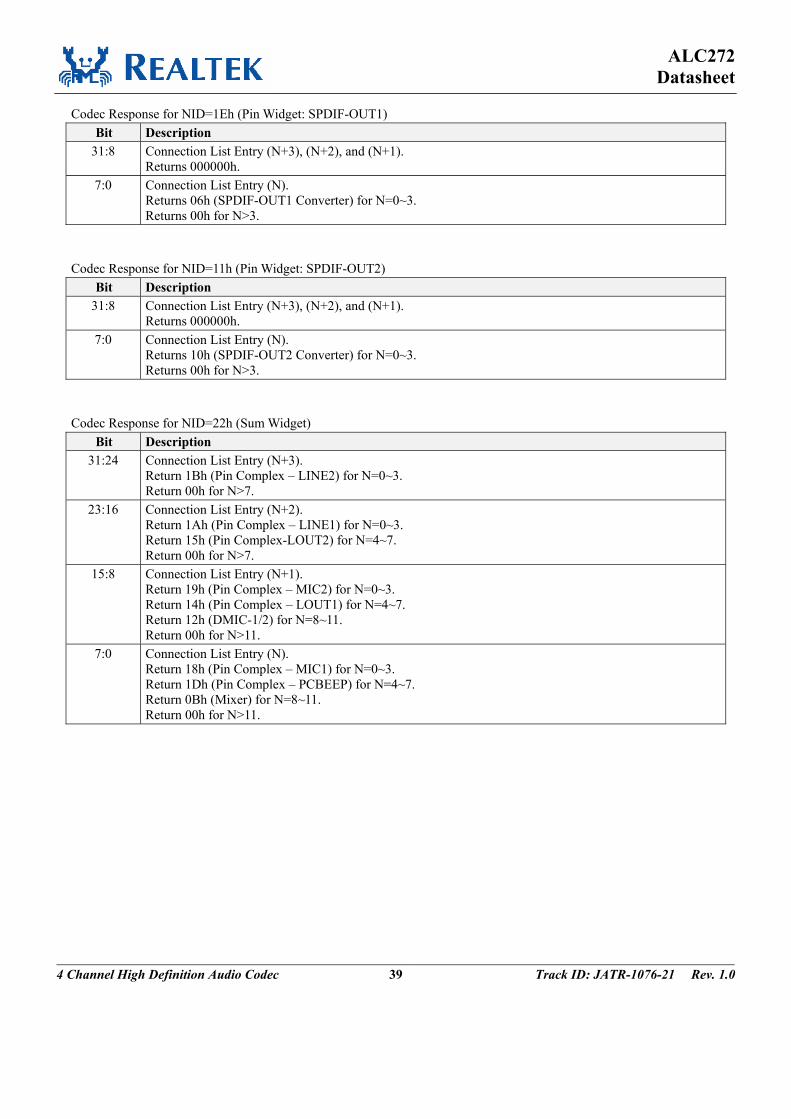
ALC272 Datasheet
4 Channel High Definition Audio Codec 39 Track ID: JATR-1076-21 Rev. 1.0
Codec Response for NID=1Eh (Pin Widget: SPDIF-OUT1) Bit Description
31:8 Connection List Entry (N+3), (N+2), and (N+1). Returns 000000h.
7:0 Connection List Entry (N). Returns 06h (SPDIF-OUT1 Converter) for N=0~3. Returns 00h for N>3.
Codec Response for NID=11h (Pin Widget: SPDIF-OUT2)
Bit Description 31:8 Connection List Entry (N+3), (N+2), and (N+1).
Returns 000000h. 7:0 Connection List Entry (N).
Returns 10h (SPDIF-OUT2 Converter) for N=0~3. Returns 00h for N>3.
Codec Response for NID=22h (Sum Widget)
Bit Description 31:24 Connection List Entry (N+3).
Return 1Bh (Pin Complex – LINE2) for N=0~3. Return 00h for N>7.
23:16 Connection List Entry (N+2). Return 1Ah (Pin Complex – LINE1) for N=0~3. Return 15h (Pin Complex-LOUT2) for N=4~7. Return 00h for N>7.
15:8 Connection List Entry (N+1). Return 19h (Pin Complex – MIC2) for N=0~3. Return 14h (Pin Complex – LOUT1) for N=4~7. Return 12h (DMIC-1/2) for N=8~11. Return 00h for N>11.
7:0 Connection List Entry (N). Return 18h (Pin Complex – MIC1) for N=0~3. Return 1Dh (Pin Complex – PCBEEP) for N=4~7. Return 0Bh (Mixer) for N=8~11. Return 00h for N>11.

ALC272 Datasheet
4 Channel High Definition Audio Codec 40 Track ID: JATR-1076-21 Rev. 1.0
Codec Response for NID=23h (Sum Widget) Bit Description
31:24 Connection List Entry (N+3). Return 1Bh (Pin Complex – LINE2) for N=0~3. Return 00h for N>7.
23:16 Connection List Entry (N+2). Return 1Ah (Pin Complex – LINE1) for N=0~3. Return 15h (Pin Complex-LOUT2) for N=4~7. Return 00h for N>7.
15:8 Connection List Entry (N+1). Return 19h (Pin Complex – MIC2) for N=0~3. Return 14h (Pin Complex – LOUT1) for N=4~7. Return 00h for N>11.
7:0 Connection List Entry (N). Return 18h (Pin Complex – MIC1) for N=0~3. Return 1Dh (Pin Complex – PCBEEP) for N=4~7. Return 0Bh (Mixer) for N=8~11. Return 00h for N>11.
Codec Response for Other NID
Bit Description 31:0 Not Supported (returns 00000000h)
8.5. Verb – Get Processing State (Verb ID=F03h) Table 39. Verb – Get Processing State (Verb ID=F03h)
Get Command Format Codec Response Format Bit [31:28] Bit [27:20] Bit [19:8] Payload Bit [7:0] Response [31:0]
CAd=X Node ID=Xh Verb ID=F03h 0’s 32-bit response
Codec Response for All NID Bit Description
31:0 Not Supported (returns 00000000h).
8.6. Verb – Set Processing State (Verb ID=703h) Table 40. Verb – Set Processing State (Verb ID=703h)
Set Command Format Codec Response Format Bit [31:28] Bit [27:20] Bit [19:8] Payload Bit [7:0] Response [31:0]
CAd=X Node ID=Xh Verb ID=703h Processing State [7:0] 0’s for all nodes
Codec Response for all NID Bit Description
31:0 0’s.

ALC272 Datasheet
4 Channel High Definition Audio Codec 41 Track ID: JATR-1076-21 Rev. 1.0
8.7. Verb – Get Coefficient Index (Verb ID=Dh) Table 41. Verb – Get Coefficient Index (Verb ID=Dh)
Get Command Format Codec Response Format Bit [31:28] Bit [27:20] Bit [19:16] Payload Bit [15:0] Response [31:0]
CAd=X Node ID=20h Verb ID=Dh 0’s Bit [15:0] are Coefficient Index
Codec Response for NID=20h (Realtek Defined Registers) Bit Description
31:16 Reserved. Read as 0’s. 15:0 Coefficient Index.
Codec Response for Other NID
Bit Description 31:0 Not Supported (returns 00000000h).
8.8. Verb – Set Coefficient Index (Verb ID=5h) Table 42. Verb – Set Coefficient Index (Verb ID=5h)
Set Command Format Codec Response Format Bit [31:28] Bit [27:20] Bit [19:16] Payload Bit [15:0] Response [31:0]
CAd=X Node ID=20h Verb ID=5h Coefficient Index [15:0] 0’s for all nodes
Codec Response for All NID Bit Description
31:0 0’s.
8.9. Verb – Get Processing Coefficient (Verb ID=Ch) Table 43. Verb – Get Processing Coefficient (Verb ID=Ch)
Get Command Format Codec Response Format Bit [31:28] Bit [27:20] Bit [19:16] Payload Bit [15:0] Response [31:0]
CAd=X Node ID=20h Verb ID=Ch 0’s Processing Coefficient [15:0]
Codec Response for NID=20h (Realtek Defined Registers) Bit Description
31:16 Reserved. Read as 0’s. 15:0 Processing Coefficient.
Codec Response for Other NID
Bit Description 31:0 Not Supported (returns 00000000h).
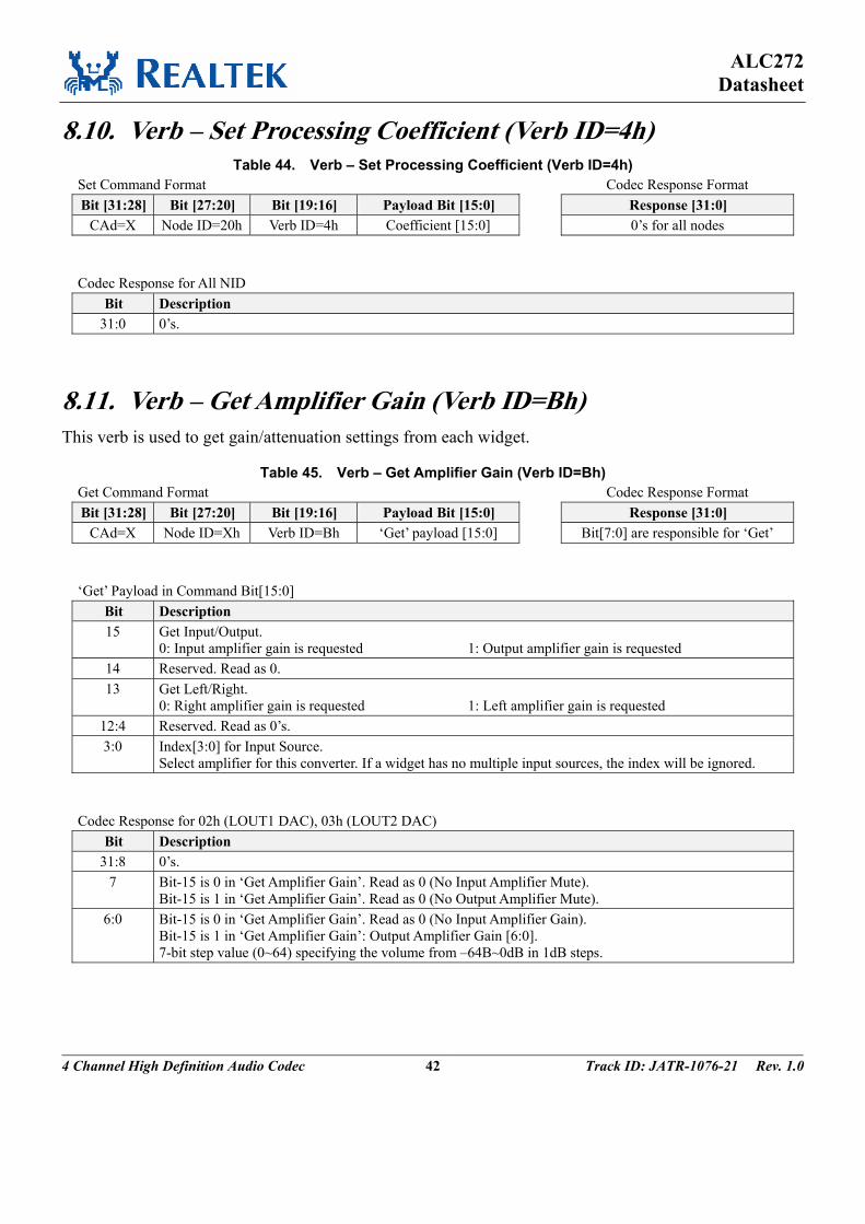
ALC272 Datasheet
4 Channel High Definition Audio Codec 42 Track ID: JATR-1076-21 Rev. 1.0
8.10. Verb – Set Processing Coefficient (Verb ID=4h) Table 44. Verb – Set Processing Coefficient (Verb ID=4h)
Set Command Format Codec Response Format Bit [31:28] Bit [27:20] Bit [19:16] Payload Bit [15:0] Response [31:0]
CAd=X Node ID=20h Verb ID=4h Coefficient [15:0] 0’s for all nodes
Codec Response for All NID
Bit Description 31:0 0’s.
8.11. Verb – Get Amplifier Gain (Verb ID=Bh) This verb is used to get gain/attenuation settings from each widget.
Table 45. Verb – Get Amplifier Gain (Verb ID=Bh) Get Command Format Codec Response Format Bit [31:28] Bit [27:20] Bit [19:16] Payload Bit [15:0] Response [31:0]
CAd=X Node ID=Xh Verb ID=Bh ‘Get’ payload [15:0] Bit[7:0] are responsible for ‘Get’
‘Get’ Payload in Command Bit[15:0]
Bit Description 15 Get Input/Output.
0: Input amplifier gain is requested 1: Output amplifier gain is requested 14 Reserved. Read as 0. 13 Get Left/Right.
0: Right amplifier gain is requested 1: Left amplifier gain is requested 12:4 Reserved. Read as 0’s. 3:0 Index[3:0] for Input Source.
Select amplifier for this converter. If a widget has no multiple input sources, the index will be ignored.
Codec Response for 02h (LOUT1 DAC), 03h (LOUT2 DAC)
Bit Description 31:8 0’s.
7 Bit-15 is 0 in ‘Get Amplifier Gain’. Read as 0 (No Input Amplifier Mute). Bit-15 is 1 in ‘Get Amplifier Gain’. Read as 0 (No Output Amplifier Mute).
6:0 Bit-15 is 0 in ‘Get Amplifier Gain’. Read as 0 (No Input Amplifier Gain). Bit-15 is 1 in ‘Get Amplifier Gain’: Output Amplifier Gain [6:0]. 7-bit step value (0~64) specifying the volume from –64B~0dB in 1dB steps.

ALC272 Datasheet
4 Channel High Definition Audio Codec 43 Track ID: JATR-1076-21 Rev. 1.0
Codec Response for 08h (ADC) Bit Description
31:8 0’s. 7 Bit-15 is 0 in ‘Get Amplifier Gain’. Input Amplifier Mute. 0: Unmute; 1: Mute
Bit-15 is 1 in ‘Get Amplifier Gain’. Read as 0 (No Output Amplifier Mute). 6:0 Bit-15 is 0 in ‘Get Amplifier Gain’. Input Amplifier Gain [6:0].
7-bit step value (0~31) specifying the volume from –16.5B~+30dB in 1.5dB steps. Bit-15 is 1 in ‘Get Amplifier Gain’. Read as 0’s (No Output Amplifier Mute).
Codec Response for 09h (ADC)
Bit Description 31:8 0’s.
7 Bit-15 is 0 in ‘Get Amplifier Gain’. Input Amplifier Mute. 0: Unmute; 1: Mute Bit-15 is 1 in ‘Get Amplifier Gain’. Read as 0 (No Output Amplifier Mute).
6:0 Bit-15 is 0 in ‘Get Amplifier Gain’. Input Amplifier Gain [6:0]. 7-bit step value (0~31) specifying the volume from –16.5B~+30dB in 1.5dB steps. Bit-15 is 1 in ‘Get Amplifier Gain’. Read as 0’s (No Output Amplifier Mute).
Codec Response for NID=0Bh (MIXER Sum Widget)
Bit Description 31:8 0’s
7 Bit-15 is 0 in ‘Get Amplifier Gain’. Input Amplifier Mute. 0: Unmute; 1: Mute (Default for all Index) Bit-15 is 1 in ‘Get Amplifier Gain’. Read as 0 (No Output Amplifier Mute).
6:0 Bit-15 is 0 in ‘Get Amplifier Gain’. Input Amplifier Gain [6:0]. 7-bit step value (0~31) specifying the volume from –34.5dB~+12dB in 1.5dB steps. Bit-15 is 1 in ‘Get Amplifier Gain’. Read as 0’s (No Output Amplifier Mute).
Codec Response for NID=0Ch~0Fh (Sum Widget: LOUT1, LOUT2, MONO)
Bit Description 31:8 0’s.
7 Bit-15 is 0 in ‘Get Amplifier Gain’. Input Amplifier Mute. 0: Unmute; 1: Mute Bit-15 is 1 in ‘Get Amplifier Gain’. Read as 0 (No Output Amplifier Mute).
6:0 Bit-15 is 0 in ‘Get Amplifier Gain’. Read as 0 (No Input Amplifier Gain). Bit-15 is 1 in ‘Get Amplifier Gain’. Read as 0 (No Output Amplifier Gain).
Codec Response for NID=14h, 15h, 17h and 21h (Pin Widget: LOUT1/LOUT2/MONO/HP-OUT)
Bit Description 31:8 0’s.
7 Bit-15 is 0 in ‘Get Amplifier Gain’. Read as 0 (No Input Amplifier Mute). Bit-15 is 1 in ‘Get Amplifier Gain’: Output Amplifier Mute. 0:Unmute; 1:Mute (Default=1)
6:0 Bit-15 is 0 in ‘Get Amplifier Gain’. Read as 0 (No Input Amplifier Gain). Bit-15 is 1 in ‘Get Amplifier Gain’. Read as 0 (No Output Amplifier Gain).

ALC272 Datasheet
4 Channel High Definition Audio Codec 44 Track ID: JATR-1076-21 Rev. 1.0
Codec Response for NID=18h, 19h, 1Ah and 1Bh (Pin Widget: MIC1/MIC2/LINE1/LINE2) Bit Description
31:8 0’s. 7 Bit-15 is 0 in ‘Get Amplifier Gain’. Read as 0 (No Input Amplifier Mute).
Bit-15 is 1 in ‘Get Amplifier Gain’: Output Amplifier Mute. 0:Unmute; 1:Mute (Default=1) 6:0 Bit-15 is 0 in ‘Get Amplifier Gain’. Input Amplifier Gain [6:0].
Specifying the boost from 0dB/10dB/20dB/30dB in 10dB per step (Default=0, 0dB). Bit-15 is 1 in ‘Get Amplifier Gain’. Read as 0 (No Output Amplifier Gain).
Codec Response for NID=22h (Sum Widget)
Bit Description 31:8 0’s
7 Bit-15 is 0 in ‘Get Amplifier Gain’. Input Amplifier Mute. 0: Unmute; 1: Mute (Default=1 for all index) Bit-15 is 1 in ‘Get Amplifier Gain’. Read as 0 (No Output Amplifier Mute).
6:0 Bit-15 is 0 in ‘Get Amplifier Gain’. Read as 0 (No Input Amplifier Gain). Bit-15 is 1 in ‘Get Amplifier Gain’. Read as 0 (No Output Amplifier Gain).
Codec Response for NID=23h (Sum Widget)
Bit Description 31:8 0’s
7 Bit-15 is 0 in ‘Get Amplifier Gain’. Input Amplifier Mute. 0: Unmute; 1: Mute (Default=1 for all index) Bit-15 is 1 in ‘Get Amplifier Gain’. Read as 0 (No Output Amplifier Mute).
6:0 Bit-15 is 0 in ‘Get Amplifier Gain’. Read as 0 (No Input Amplifier Gain). Bit-15 is 1 in ‘Get Amplifier Gain’. Read as 0 (No Output Amplifier Gain).
Codec Response to Other NID
Bit Description 31:0 Not Supported (returns 00000000h).

ALC272 Datasheet
4 Channel High Definition Audio Codec 45 Track ID: JATR-1076-21 Rev. 1.0
8.12. Verb – Set Amplifier Gain (Verb ID=3h) This verb is used to set amplifier gain/attenuation in each widget.
Table 46. Verb – Set Amplifier Gain (Verb ID=3h) Set Command Format Codec Response Format Bit [31:28] Bit [27:20] Bit [19:8] Payload Bit [7:0] Response [31:0]
CAd=X Node ID=Xh Verb ID=3h ‘Set’ payload [7:0] 0’s for all nodes
‘Set’ Payload in Command Bit[15:0]
Bit Description 15 Set Output Amp.
1: Indicates output amplifier gain will be set 14 Set Input Amp.
1: Indicates input amplifier gain will be set 13 Set Left Amp.
1: Indicates left amplifier gain will be set 12 Set Right Amp.
1: Indicates right amplifier gain will be set 11:8 Index Offset (for input amplifiers on Sum widgets and Selector Widgets).
5-bit index offset in connection list is used to select the input gain that will be set on a Sum or a Selector widget. The index is ignored if the node is not a Sum or a Selector widget, or the ‘Set Input Amp’ bit is not set.
7 Mute. 0: Unmute 1: Mute (-∞gain)
6:0 Gain[6:0]. A 7-bit step value specifying the amplifier gain

ALC272 Datasheet
4 Channel High Definition Audio Codec 46 Track ID: JATR-1076-21 Rev. 1.0
8.13. Verb – Get Converter Format (Verb ID=Ah) Table 47. Verb – Get Converter Format (Verb ID=Ah)
Get Command Format Codec Response Format Bit [31:28] Bit [27:20] Bit [19:16] Payload Bit [15:0] Response [31:0]
CAd=X Node ID=Xh Verb ID=Ah 0’s Bit[15:0] are converter format
Codec Response for NID=02h~03h, 06h, 10h (Output Converters: LOUT1, LOUT2 DAC and SPDIF-OUT1/2). Codec Response for NID=08h and 09h (Input Converters: ADC 08h and ADC 09h)
Bit Description 31:16 Reserved. Read as 0.
15 Stream Type (TYPE). 0: PCM 1: Non-PCM
14 Sample Base Rate (BASE). 0: 48kHz 1: 44.1kHz
13:11 Sample Base Rate Multiple (MULT). 000b: *1 001b: *2 010b: *3 011b: *4 100b~111b: Reserved
10:8 Sample Base Rate Divisor (DIV). 000b: /1 001b: /2 010b: /3 011b: /4 100b: /5 101b: /6 110b: /7 111b: /8 Not supported. Always read as 000b.
7 Reserved. Read as 0. 6:4 Bits per Sample (BITS).
000b: 8 bits 001b: 16 bits 010b: 20 bits 011b: 24 bits 100b: 32 bits 101b~111b: Reserved
3:0 Number of Channels. 0: 1 channel 1: 2 channels 2: 3 channels ……… 15: 16 channels
Table 48. Get Converter Format Support
BASE MULT DIV BITS Sample rate 0 000b, 001b, 011b 000b 001,010b, 011b 48K, 96K, 192K NID=02h (LOUT1 DAC) 1 000b 000b 001,010b, 011b 44.1K 0 000b, 001b, 011b 000b 001,010b, 011b 48K, 96K, 192K NID=03h (LOUT2 DAC) 1 000b 000b 001,010b, 011b 44.1K 0 000b, 001b, 011b 000b 001,010b, 011b 48K, 96K, 192K NID=06h (SPDIF-OUT1) 1 000b, 001b 000b 001,010b, 011b 44.1K, 88.2K 0 000b, 001b, 011b 000b 001,010b, 011b 48K, 96K, 192K NID=10h (SPDIF-OUT2) 1 000b, 001b 000b 001,010b, 011b 44.1K, 88.2K 0 000b, 001b, 011b 000b 001,010b, 011b 48K, 96K, 192K NID=08h (LINE ADC) 1 000b 000b 001,010b, 011b 44.1K 0 000b, 001b, 011b 000b 001,010b, 011b 48K, 96K, 192K NID=09h (MIX ADC) 1 000b 000b 001,010b, 011b 44.1K
Codec Response for other NID
Bit Description 31:0 Not Supported (returns 00000000h).

ALC272 Datasheet
4 Channel High Definition Audio Codec 47 Track ID: JATR-1076-21 Rev. 1.0
8.14. Verb – Set Converter Format (Verb ID=2h) Table 49. Verb – Set Converter Format (Verb ID=2h)
Set Command Format Codec Response Format Bit [31:28] Bit [27:20] Bit [19:16] Payload Bit [15:0] Response [31:0]
CAd=X Node ID=Xh Verb ID=2h Set format [15:0] 0’s for all nodes
‘Set’ Payload in Command Bit[15:0]
Bit Description 31:16 Reserved. Read as 0.
15 Stream Type (TYPE). 0: PCM 1: Non-PCM
14 Sample Base Rate (BASE). 0: 48kHz 1: 44.1kHz
13:11 Sample Base Rate Multiple (MULT). 000b: *1 001b: *2 010b: *3 011b: *4 100b~111b: Reserved
10:8 Sample Base Rate Divisor (DIV). 000b: /1 001b: /2 010b: /3 011b: /4 100b: /5 101b: /6 110b: /7 111b: /8
7 Reserved. Read as 0. 6:4 Bits per Sample (BITS).
000b: 8 bits 001b: 16 bits 010b: 20 bits 011b: 24 bits 100b: 32 bits 101b~111b: Reserved
3:0 Number of Channels. 0: 1 channel 1: 2 channels 2: 3 channels ……… 15: 16 channels

ALC272 Datasheet
4 Channel High Definition Audio Codec 48 Track ID: JATR-1076-21 Rev. 1.0
8.15. Verb – Get Power State (Verb ID=F05h) The ALC272 is designed to meet Intel’s low-power-state white paper and is ECR HDA-015B compliant (see section 7.5 Power Management , page 24).
Table 50. Verb – Get Power State (Verb ID=F05h) Get Command Format Codec Response Format Bit [31:28] Bit [27:20] Bit [19:8] Payload Bit [7:0] Response [31:0]
CAd=X Node ID=Xh Verb ID= F05h 0’s Power State [7:0]
Codec Response for NID=01h (Audio Function Group) Codec Response for NID=02h, 03h, 08h, 09h (Analog Input/Output Converter) Codec Response for NID=11h, 12h, 14h, 15h, 17h, 18h, 19h, 1Ah, 1Bh, 1Dh, 1Eh, 21h (Pin Widgets) Codec Response for NID=06h, 10h (Digital Output Converter)
Bit Description 31:11 Reserved. Read as 0’s.
10 PS-SettingsReset. 0: Setting of widgets have been reset during low power state 1: Setting changed from the default were reset to their default during low power state
9 PS-ClkStopOk. 0: No capability to operate normally with BITCLK stop 1: Operate properly with no BICLK
8 PS-Error. No support in ALC272
7:6 Reserved. Read as 0’s. 5:4 PS-Act. Actual Power State [1:0].
00: Power state is D0 01: Power state is D1 10: Power state is D2 11: Power state is D3 PS-Act indicates the actual power state of the referenced node. For Audio Function Group nodes (NID=01h), PS-Act is always equal to PS-Set.
3:2 Reserved. Read as 0’s. 1:0 PS-Set. Set Power State [1:0].
00: Power state is D0 01: Power state is D1 10: Power state is D2 11: Power state is D3 PS-Set controls the current power setting of the referenced node.
Codec Response for other NID
Bit Description 31:0 Not Supported (returns 00000000h).

ALC272 Datasheet
4 Channel High Definition Audio Codec 49 Track ID: JATR-1076-21 Rev. 1.0
8.16. Verb – Set Power State (Verb ID=705h) Table 51. Verb – Set Power State (Verb ID=705h)
Set Command Format Codec Response Format Bit [31:28] Bit [27:20] Bit [19:8] Payload Bit [7:0] Response [31:0]
CAd=X Node ID=Xh Verb ID=705h Power State [7:0] 0’s for all nodes
‘Power State’ in Command Bit[7:0]
Bit Description 7:6 Reserved. Read as 0’s. 5:4 PS-Act. Actual Power State [1:0].
00: Power state is D0 01: Power state is D1 10: Power state is D2 11: Power state is D3 PS-Act indicates the actual power state of the referenced node.
3:2 Reserved. Read as 0’s. 1:0 PS-Set. Set Power State [1:0].
00: Power state is D0 01: Power state is D1 10: Power state is D2 11: Power state is D3
8.17. Verb – Get Converter Stream, Channel (Verb ID=F06h) Table 52. Verb – Get Converter Stream, Channel (Verb ID=F06h)
Get Command Format Codec Response Format Bit [31:28] Bit [27:20] Bit [19:8] Payload Bit [7:0] Response [31:0]
CAd=X Node ID=Xh Verb ID=F06h 0’s Stream & Channel [7:0]
Codec Response for NID=02h~03h, 06h and 10h (Output Converters: LOUT1, LOUT2 DAC, and SPDIF-OUT1/2) Codec Response for NID=08h and 09h (Input Converters: LINE, MIX ADC)
Bit Description 31:8 Reserved. Read as 0’s. 7:4 Stream[3:0].
The link stream used by the converter. 0000b is unused, 0001b is stream 1, etc. 3:0 Channel[3:0].
The lowest channel used by the converter. A stereo converter will use the set channel n as well as n+1 for its left and right channel.
Codec Response for other NID
Bit Description 31:0 Not Supported (returns 00000000h).

ALC272 Datasheet
4 Channel High Definition Audio Codec 50 Track ID: JATR-1076-21 Rev. 1.0
8.18. Verb – Set Converter Stream, Channel (Verb ID=706h) Table 53. Verb – Set Converter Stream, Channel (Verb ID=706h)
Set Command Format Codec Response Format Bit [31:28] Bit [27:20] Bit [19:8] Payload Bit [7:0] Response [31:0]
CAd=X Node ID=Xh Verb ID=706h Stream & Channel [7:0] 0’s for all nodes
‘Stream and Channel’ in Command Bit[7:0] Bit Description
31:8 Reserved. Read as 0’s. 7:4 Set Stream[3:0]. The link stream used by the converter. 0000b is stream 0, 0001b is stream 1, etc. 1:0 Set Channel[3:0]. The lowest channel used by the converter. A stereo converter will use the set channel n as
well as n+1 for its left and right channel.
8.19. Verb – Get Pin Widget Control (Verb ID=F07h) Table 54. Verb – Get Pin Widget Control (Verb ID=F07h)
Get Command Format Codec Response Format Bit [31:28] Bit [27:20] Bit [19:8] Payload Bit [7:0] Response [31:0]
CAd=X Node ID=Xh Verb ID=F07h 0’s Pin Control [7:0]
Codec Response for NID=11h, 12h, 14h, 15h, 17h, 18h, 19h, 1Ah, 1Bh, 1Dh, 1Eh, 21h (Pin Complex) Bit Description
31:8 Reserved. Read as 0’s. 7 H-Phn Enable.
0: Disabled 1: Enabled Note: Only NID=14h, 15h, 19A, 1Bh and 21h support headphone amplifier.
6 Out Enable (Output Buffet Enable, EN_OBUF for an I/O unit). 0: Disabled 1: Enabled Note: NID= 1Dh (PCBEEP) do not support output and are always read 0.
5 In Enable (Input Buffer Enable, EN_IBUF for an I/O unit). 0: Disabled 1: Enabled Note: NID=1Eh (1st SPDIF-OUT) and 11h (2nd SPDIF-OUT) do not support output and is always read 0.
4:3 Reserved. 2:0 VrefEn (Vrefout Enable Control).
000b: Hi-Z (Disabled, default for all) 001b: 50% of AVDD (ALC272 supports 2.5V reference output when AVDD is 5V) 010b: Ground 0V 011b: Reserved 100b: 80% of AVDD (ALC272 supports 3.2V reference output when AVDD is 5V) 101b: 100% of AVDD 110b~111b: Reserved Note: Only NID=18h, 19h, 1Ah, and 1Bh support reference output, other nodes will ignore this verb and respond with 0.
Codec Response for other NID
Bit Description 31:0 Not Supported (returns 00000000h).
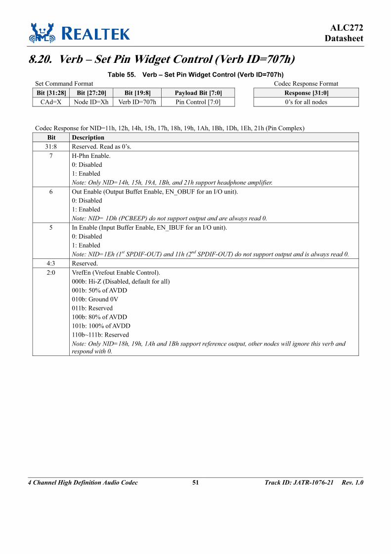
ALC272 Datasheet
4 Channel High Definition Audio Codec 51 Track ID: JATR-1076-21 Rev. 1.0
8.20. Verb – Set Pin Widget Control (Verb ID=707h) Table 55. Verb – Set Pin Widget Control (Verb ID=707h)
Set Command Format Codec Response Format Bit [31:28] Bit [27:20] Bit [19:8] Payload Bit [7:0] Response [31:0]
CAd=X Node ID=Xh Verb ID=707h Pin Control [7:0] 0’s for all nodes
Codec Response for NID=11h, 12h, 14h, 15h, 17h, 18h, 19h, 1Ah, 1Bh, 1Dh, 1Eh, 21h (Pin Complex)
Bit Description 31:8 Reserved. Read as 0’s.
7 H-Phn Enable. 0: Disabled 1: Enabled Note: Only NID=14h, 15h, 19A, 1Bh, and 21h support headphone amplifier.
6 Out Enable (Output Buffet Enable, EN_OBUF for an I/O unit). 0: Disabled 1: Enabled Note: NID= 1Dh (PCBEEP) do not support output and are always read 0.
5 In Enable (Input Buffer Enable, EN_IBUF for an I/O unit). 0: Disabled 1: Enabled Note: NID=1Eh (1st SPDIF-OUT) and 11h (2nd SPDIF-OUT) do not support output and is always read 0.
4:3 Reserved. 2:0 VrefEn (Vrefout Enable Control).
000b: Hi-Z (Disabled, default for all) 001b: 50% of AVDD 010b: Ground 0V 011b: Reserved 100b: 80% of AVDD 101b: 100% of AVDD 110b~111b: Reserved Note: Only NID=18h, 19h, 1Ah and 1Bh support reference output, other nodes will ignore this verb and respond with 0.

ALC272 Datasheet
4 Channel High Definition Audio Codec 52 Track ID: JATR-1076-21 Rev. 1.0
8.21. Verb – Get Unsolicited Response Control (Verb ID=F08h) Determines whether a widget is enabled to send an unsolicited response. An HDA codec can use an unsolicited response to inform software of a real-time event.
Table 56. Verb – Get Unsolicited Response Control (Verb ID=F08h) Get Command Format Codec Response Format Bit [31:28] Bit [27:20] Bit [19:8] Payload Bit [7:0] Response [31:0]
CAd=X Node ID=Xh Verb ID= F08h 0’s 32-bit Response
Codec Response for NID=01h (GPIO), 14h, 15h, 18h~1Bh, 21h (Pin Complex)
Bit Description 31:8 Reserved. Read as 0’s.
7 Unsolicited Response is Enabled. 0: Disabled 1: Enabled
6:4 Reserved. Read as 0’s. 3:0 Assigned Tag for Unsolicited Response.
The tag[3:0] is assigned by software to determine which widget generates unsolicited responses.
Codec Response for other NID
Bit Description 31:0 Not Supported (returns 00000000h).
8.22. Verb – Set Unsolicited Response Control (Verb ID=708h) Enable a widget to generate an unsolicited response.
Table 57. Verb – Set Unsolicited Response Control (Verb ID=708h) Set Command Format Codec Response Format Bit [31:28] Bit [27:20] Bit [19:8] Payload Bit [7:0] Response [31:0]
CAd=X Node ID=Xh Verb ID=708h EnableUnsol [7:0] 0’s for all nodes
‘EnableUnsol’ in Command Bit [7:0]
Bit Description 31:8 Reserved. Read as 0’s.
7 Unsolicited Response. 0: Disable 1: Enable
6 Reserved. Read as 0’s. 5:0 Tag for Unsolicited Responses.
Tag[5:0] is defined by software to assign a 6-bit tag for nodes that are enabled to generate unsolicited responses.

ALC272 Datasheet
4 Channel High Definition Audio Codec 53 Track ID: JATR-1076-21 Rev. 1.0
8.23. Verb – Get Pin Sense (Verb ID=F09h) Returns the Presence Detect status and the impedance of a device attached to the pin.
Table 58. Verb – Get Pin Sense (Verb ID=F09h) Get Command Format Codec Response Format Bit [31:28] Bit [27:20] Bit [19:8] Payload Bit [7:0] Response [31:0]
CAd=X Node ID=Xh Verb ID= F09h 0’s 32-bit Response
Codec Response for NID=14h, 15h, 18h, 19h, 1Ah, 1Bh, 21h
Bit Description 31 Presence Detect Status.
0: No device is attached to the pin 1: Device is attached to the pin
30:0 Measured Impedance. The ALC272 does not support hardware impedance detect. This field is read as 0s.
Codec Response for other NID
Bit Description 31:0 Not Supported (returns 00000000h).
8.24. Verb – Execute Pin Sense (Verb ID=709h) Table 59. Verb – Execute Pin Sense (Verb ID=709h)
Command Format Codec Response Format Bit [31:28] Bit [27:20] Bit [19:8] Payload Bit [7:0] Response [31:0]
CAd=X Node ID=Xh Verb ID= 709h Right Channel[0] 0’s for all nodes
‘Payload’ in Command Bit[7:0] (for NID=14h, 15h, 18h, 19h, 1Ah, 1Bh, 21h)
Bit Description 7:1 Reserved. Read as 0’s. 0 Right (Ring) Channel Select.
0: Sense Left Channel (Tip) 1: Sense Right Channel (Ring) The ALC272 does not support hardware impedance detect and will ignore this control bit.

ALC272 Datasheet
4 Channel High Definition Audio Codec 54 Track ID: JATR-1076-21 Rev. 1.0
8.25. Verb – Get Configuration Default (Verb ID=F1Ch/F1Dh/F1Eh/F1Fh)
Read the 32-bit sticky register for each Pin Widget configured by software.
Table 60. Verb – Get Configuration Default (Verb ID=F1Ch/F1Dh/F1Eh/F1Fh) Get Command Format Codec Response Format Bit [31:28] Bit [27:20] Bit [19:8] Payload Bit [7:0] Response [31:0]
CAd=X Node ID=Xh Verb ID= F1Ch 0’s 32-bit Response
Codec Response for NID=14h, 15h, 17h, 18h, 19h, 1Ah, 1Bh, 21h, 1Dh, 1Eh, 11h, 12h (Pin Widget: LOUT1, LOUT2, MONO, MIC1, MIC2, LINE1, LINE2, PCBEEP, HP-OUT, SPDIF-OUT1, SPDIF-OUT2, DMIC1/2)
Bit Description 31:0 32-bit configuration information for each pin widget.
Note: The 32-bit registers for each Pin Widget are sticky and will not be reset by a LINK Reset or Codec Reset (Function Reset Verb).
8.26. Verb – Set Configuration Default Bytes 0, 1, 2, 3 (Verb ID=71Ch/71Dh/71Eh/71Fh)
The BIOS can use this verb to figure out the default conditions (e.g., placement and expected default device) for the Pin Widgets NID=0B~0Fh, 10h, 11h, 1Fh, 20h, and 12h.
Table 61. Verb – Set Configuration Default Bytes 0, 1, 2, 3 (Verb ID=71Ch/71Dh/71Eh/71Fh) Set Command Format Codec Response Format Bit [31:28] Bit [27:20] Bit [19:8] Payload Bit [7:0] Response [31:0]
CAd=X Node ID=Xh Verb ID=71Ch, 71Dh, 71Eh, 71Fh
Label [7:0] 0’s for all nodes
Note: Supported by Pin Widget NID=14h, 15h, 17h, 18h, 19h, 1Ah, 1Bh, 21h, 1Dh, 1Eh, 11h, 12h. Other widgets will ignore this verb.
Codec Response for All NID
Bit Description 31:0 0’s.

ALC272 Datasheet
4 Channel High Definition Audio Codec 55 Track ID: JATR-1076-21 Rev. 1.0
8.27. Verb – Get BEEP Generator (Verb ID=F0Ah) Table 62. Verb – Get BEEP Generator (Verb ID= F0Ah)
Get Command Format Codec Response Format Bit [31:28] Bit [27:20] Bit [19:8] Payload Bit [7:0] Response [31:0]
CAd=X Node ID=01h Verb ID= F1Bh 0’s Divider [7:0]
‘Response’ for NID=01h
Bit Description 31:8 Reserved. 7:0 Frequency Divider, F[7:0].
The internal BEEP frequency is the result of dividing the 48kHz clock by 4 times the number specified in F[7:0]. The lowest tone is 48kHz/(255*4)=47Hz. The highest tone is 48kHz/(1*4)=12kHz. A value of 00h in F[7:0] disables the internal BEEP generator and allows external PCBEEP input.
Codec Response for Other NID
Bit Description 31:0 0’s.
8.28. Verb – Set BEEP Generator (Verb ID=70Ah) Table 63. Verb – Set BEEP Generator (Verb ID= 70Ah)
Set Command Format Codec Response Format Bit [31:28] Bit [27:20] Bit [19:8] Payload Bit [7:0] Response [31:0]
CAd=X Node ID=01h Verb ID=71Bh Divider [7:0] 0’s for all nodes
‘Divider’ in Set Command
Bit Description 31:8 Reserved. 7:0 Frequency Divider, F[7:0].
The internal BEEP frequency is the result of dividing the 48kHz clock by 4 times the number specified in F[7:0]. The lowest tone is 48kHz/(255*4)=47Hz. The highest tone is 48kHz/(1*4)=12kHz. A value of 00h in F[7:0] disables the internal BEEP generator and allows external PCBEEP input.
Note: All nodes except BEEP generator (NID=01h) will ignore this verb.
Codec Response for All NID
Bit Description 31:0 0’s.

ALC272 Datasheet
4 Channel High Definition Audio Codec 56 Track ID: JATR-1076-21 Rev. 1.0
8.29. Verb – Get GPIO Data (Verb ID= F15h) Table 64. Verb – Get GPIO Data (Verb ID= F15h)
Get Command Format Codec Response Format Bit [31:28] Bit [27:20] Bit [19:8] Payload Bit [7:0] Response [31:0]
CAd=X Node ID=01h Verb ID=F15h 0’s 32-bit Response
Codec Response for NID=01h (Audio Function Group)
Bit Description 31:8 Reserved. 7:2 Reserved. 1:0 GPIO[1:0] Data.
The value written (output) or sensed (input) on the corresponding pin if it is enabled.
Codec Response for Other NID
Bit Description 31:0 0’s.
8.30. Verb – Set GPIO Data (Verb ID= 715h) Table 65. Verb – Set GPIO Data (Verb ID= 715h)
Set Command Format Codec Response Format Bit [31:28] Bit [27:20] Bit [19:8] Payload Bit [7:0] Response [31:0]
CAd=X Node ID=01h Verb ID=715h Data [7:0] 0’s for all nodes
‘Data’ in Set command for NID=01h (Audio Function Group)
Bit Description 31:8 Reserved. 7:2 Reserved. 1:0 GPIO[1:0] Output Data.
The value written determines the value driven on a pin that is configured as an output pin.
Codec Response for All NID
Bit Description 31:0 0’s.

ALC272 Datasheet
4 Channel High Definition Audio Codec 57 Track ID: JATR-1076-21 Rev. 1.0
8.31. Verb – Get GPIO Enable Mask (Verb ID=F16h) Table 66. Verb – Get GPIO Enable Mask (Verb ID= F16h)
Get Command Format Codec Response Format Bit [31:28] Bit [27:20] Bit [19:8] Payload Bit [7:0] Response [31:0]
CAd=X Node ID=01h Verb ID=F16h 0’s EnableMask [7:0]
Codec Response for NID=01h (Audio Function Group)
Bit Description 31:8 Reserved. 7:2 Reserved. 1:0 GPIO[1:0] Enable Mask.
0: The corresponding GPIO pin is disabled and is in Hi-Z state 1: The corresponding GPIO pin is enabled. Its behavior is determined by the GPIO direction control
Note: All nodes except Audio Function Group (NID=01h) will ignore this verb.
Codec Response for Other NID
Bit Description 31:0 0’s.
8.32. Verb – Set GPIO Enable Mask (Verb ID=716h) Table 67. Verb – Set GPIO Enable Mask (Verb ID=716h)
Set Command Format Codec Response Format Bit [31:28] Bit [27:20] Bit [19:8] Payload Bit [7:0] Response [31:0]
CAd=X Node ID=01h Verb ID=716h Enable Mask [7:0] 0’s for all nodes
Codec Response for NID=01h (Audio Function Group)
Bit Description 31:8 Reserved. 7:2 Reserved. 1:0 GPIO[1:0] Enable Mask.
0: The corresponding GPIO pin is disabled and is in Hi-Z state 1: The corresponding GPIO pin is enabled. Its behavior is determined by the GPIO direction control
Note: All nodes except Audio Function Group (NID=01h) will ignore this verb.
Codec Response for All NID
Bit Description 31:0 0’s.

ALC272 Datasheet
4 Channel High Definition Audio Codec 58 Track ID: JATR-1076-21 Rev. 1.0
8.33. Verb – Get GPIO Direction (Verb ID=F17h) Table 68. Verb – Get GPIO Direction (Verb ID=F17h)
Get Command Format Codec Response Format Bit [31:28] Bit [27:20] Bit [19:8] Payload Bit [7:0] Response [31:0]
CAd=X Node ID=01h Verb ID=F17h 0’s Direction [7:0]
Codec Response for NID=01h (Audio Function Group)
Bit Description 31:8 Reserved. 7:2 Reserved. 1:0 GPIO[1:0] Direction Control.
0: The corresponding GPIO pin is configured as an input 1: The corresponding GPIO pin is configured as an output
Note: All nodes except Audio Function Group (NID=01h) will ignore this verb.
Codec Response for Other NID
Bit Description 31:0 0’s.
8.34. Verb – Set GPIO Direction (Verb ID=717h) Table 69. Verb – Set GPIO Direction (Verb ID=717h)
Set Command Format Codec Response Format Bit [31:28] Bit [27:20] Bit [19:8] Payload Bit [7:0] Response [31:0]
CAd=X Node ID=01h Verb ID=717h Direction [7:0] 0’s for all nodes
Codec Response for NID=01h (Audio Function Group)
Bit Description 31:8 Reserved. 7:2 Reserved. 1:0 GPIO[1:0] Direction Control.
0: The corresponding GPIO pin is configured as an input 1: The corresponding GPIO pin is configured as an output
Note: All nodes except Audio Function Group (NID=01h) will ignore this verb.
Codec Response for Other NID
Bit Description 31:0 0’s.

ALC272 Datasheet
4 Channel High Definition Audio Codec 59 Track ID: JATR-1076-21 Rev. 1.0
8.35. Verb – Get GPIO Unsolicited Response Enable Mask (Verb ID=F19h)
Table 70. Verb – Get GPIO Unsolicited Response Enable Mask (Verb ID=F19h) Get Command Format Codec Response Format Bit [31:28] Bit [27:20] Bit [19:8] Payload Bit [7:0] Response [31:0]
CAd=X Node ID=01h Verb ID=F19h 0’s UnsolEnable [7:0]
Codec Response for NID=01h (Audio Function Group) Bit Description
31:8 Reserved. 7:2 Reserved. 1:0 GPIO[1:0] Unsolicited Enable Mask.
0: Unsolicited response will not be sent on link 1: Unsolicited response will be sent on link when state of corresponding GPIO has been changed
Note: All nodes except Audio Function Group (NID=01h) will ignore this verb.
Codec Response for Other NID Bit Description
31:0 0’s.
8.36. Verb – Set GPIO Unsolicited Response Enable Mask (Verb ID=719h)
Table 71. Verb – Set GPIO Unsolicited Response Enable Mask (Verb ID=719h) Set Command Format Codec Response Format Bit [31:28] Bit [27:20] Bit [19:8] Payload Bit [7:0] Response [31:0]
CAd=X Node ID=01h Verb ID=719h UnsolEnable [7:0] 0’s for all nodes
Codec Response for NID=01h (Audio Function Group) Bit Description
31:8 Reserved. 7:2 Reserved. 1:0 GPIO[1:0] Unsolicited Enable Mask.
0: Unsolicited response will not be sent on link 1: Unsolicited response will be sent on link when state of corresponding GPIO has been changed
Note 1: All nodes except the Audio Function Group (NID=01h) will ignore this verb. Note 2: The unsolicited response of corresponding GPIO is enabled when it’s ‘Enable Mask’ and Verb-‘Unsolicited Response’ for NID=01h are enabled.
Codec Response for Other NID
Bit Description 31:0 0’s.

ALC272 Datasheet
4 Channel High Definition Audio Codec 60 Track ID: JATR-1076-21 Rev. 1.0
8.37. Verb – Get Digital Converter Control 1 & Control 2 (Verb ID= F0Dh, F0Eh)
Table 72. Verb – Get Digital Converter Control 1 & Control 2 (Verb ID= F0Dh, F0Eh) Get Command Format Codec Response Format Bit [31:28] Bit [27:20] Bit [19:8] Payload Bit [7:0] Response [31:0]
CAd=X Node ID=06h Verb ID=F0Dh/F0Eh 0’s Bit[31:16]=0’s, Bit[15:0] are SIC bit
NID=06h (SPDIF-OUT1 Converter) and 10h (SPDIF-OUT2 Converter) Response to ‘Get verb’ – F0Dh (Control for SIC bit[15:0])
Bit Description – SIC (SPDIF IEC Control) Bit[7:0] 31:16 Read as 0’s.
15 Reserved. Read as 0’s. 14:8 CC[6:0] (Category Code).
7 LEVEL (Generation Level). 6 PRO (Professional or Consumer Format).
0: Consumer format 1: Professional format
5 /AUDIO (Non-Audio Data Type). 0: PCM data 1: AC3 or other digital non-audio data
4 COPY (Copyright). 0: Asserted 1: Not asserted
3 PRE (Pre-Emphasis). 0: None 1: Filter pre-emphasis is 50/15 microseconds
2 VCFG for Validity Control (control V bit and data in Sub-Frame). 1 V for Validity Control (control V bit and data in Sub-Frame). 0 Digital Enable. DigEn.
0: OFF 1: ON
Codec Response for Other NID
Bit Description 31:0 0’s

ALC272 Datasheet
4 Channel High Definition Audio Codec 61 Track ID: JATR-1076-21 Rev. 1.0
8.38. Verb – Set Digital Converter Control 1 & Control 2 (Verb ID=70Dh, 70Eh)
Table 73. Verb – Set Digital Converter Control 1 & Control 2 (Verb ID=70Dh, 70Eh) Set Command Format (Verb ID=70Dh, Set Control 1) Codec Response Format Bit [31:28] Bit [27:20] Bit [19:8] Payload Bit [7:0] Response [31:0]
CAd=X Node ID=06h Verb ID=70Dh SIC [7:0] 0’s
Set Command Format (Verb ID=70Eh, Set Control 2) Codec Response Format Bit [31:28] Bit [27:20] Bit [19:8] Payload Bit [7:0] Response [31:0]
CAd=X Node ID=06h Verb ID=70Eh SIC [15:8] 0’s
‘Payload’ in Set Control 1 for NID=06h (SPDIF-OUT1 Converter) and 10h (SPDIF-OUT2 Converter)
Bit Description – SIC (SPDIF IEC Control) Bit[7:0] 7 LEVEL (Generation Level) 6 PRO (Professional or Consumer Format).
0: Consumer format 1: Professional format
5 /AUDIO (Non-Audio Data Type). 0: PCM data 1: AC3 or other digital non-audio data
4 COPY (Copyright). 0: Asserted 1: Not asserted
3 PRE (Pre-Emphasis). 0: None 1: Filter pre-emphasis is 50/15 microseconds
2 VCFG for Validity Control (control V bit and data in Sub-Frame). 1 V for Validity Control (control V bit and data in Sub-Frame). 0 Digital Enable. DigEn.
0: OFF 1: ON
‘Payload’ in Set Control 2 for NID=06h (SPDIF-OUT1 Converter) and 10h (SPDIF-OUT2 Converter)
Bit Description – SIC (SPDIF IEC Control) Bit[7:0] 7 Reserved. Read as 0’s.
6:0 CC[6:0] (Category Code).
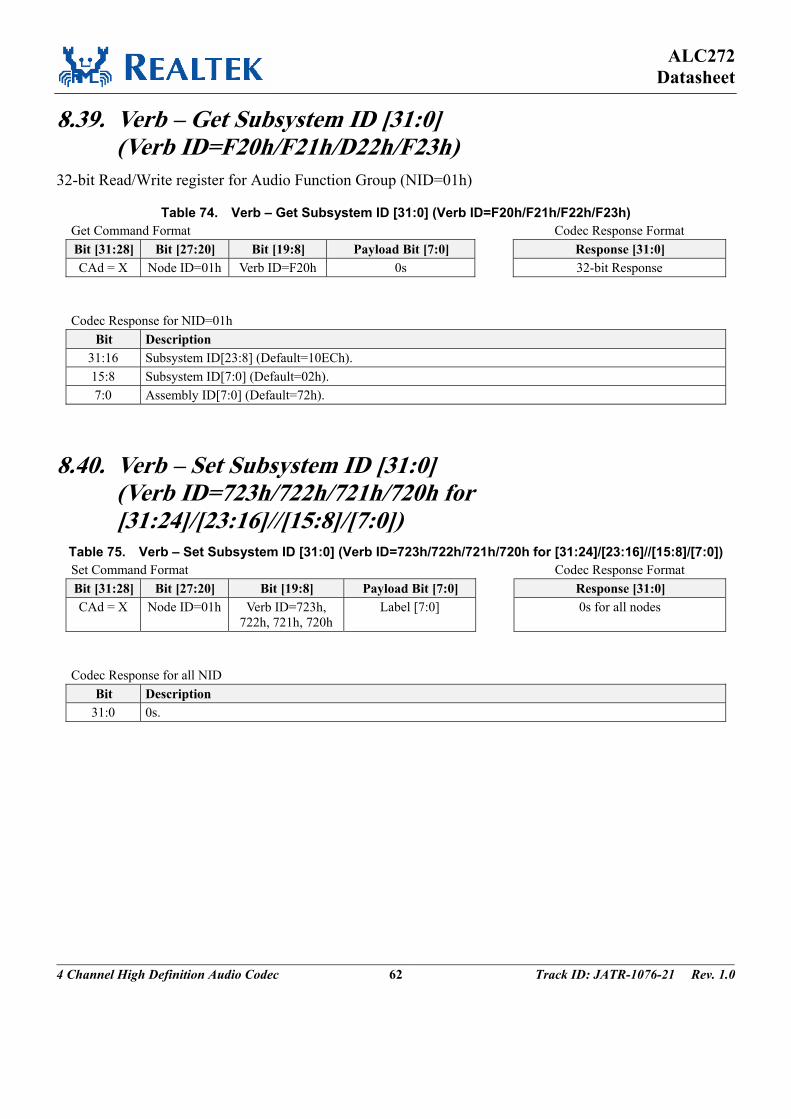
ALC272 Datasheet
4 Channel High Definition Audio Codec 62 Track ID: JATR-1076-21 Rev. 1.0
8.39. Verb – Get Subsystem ID [31:0] (Verb ID=F20h/F21h/D22h/F23h)
32-bit Read/Write register for Audio Function Group (NID=01h)
Table 74. Verb – Get Subsystem ID [31:0] (Verb ID=F20h/F21h/F22h/F23h) Get Command Format Codec Response Format Bit [31:28] Bit [27:20] Bit [19:8] Payload Bit [7:0] Response [31:0] CAd = X Node ID=01h Verb ID=F20h 0s 32-bit Response
Codec Response for NID=01h
Bit Description 31:16 Subsystem ID[23:8] (Default=10ECh). 15:8 Subsystem ID[7:0] (Default=02h). 7:0 Assembly ID[7:0] (Default=72h).
8.40. Verb – Set Subsystem ID [31:0] (Verb ID=723h/722h/721h/720h for [31:24]/[23:16]//[15:8]/[7:0])
Table 75. Verb – Set Subsystem ID [31:0] (Verb ID=723h/722h/721h/720h for [31:24]/[23:16]//[15:8]/[7:0]) Set Command Format Codec Response Format Bit [31:28] Bit [27:20] Bit [19:8] Payload Bit [7:0] Response [31:0] CAd = X Node ID=01h Verb ID=723h,
722h, 721h, 720h Label [7:0] 0s for all nodes
Codec Response for all NID
Bit Description 31:0 0s.

ALC272 Datasheet
4 Channel High Definition Audio Codec 63 Track ID: JATR-1076-21 Rev. 1.0
8.41. Verb – Get/Set EAPD Control (Verb ID=F0Ch for Get, 70Ch for Set)
Table 76. Verb – Get EAPD Control (Verb ID=F0Ch) Get Command Format (NID=14h and 15h) Codec Response Format Bit [31:28] Bit [27:20] Bit [19:8] Payload Bit [7:0] Response [31:0]
CAd=X Node ID=14h/15h Verb ID=F0Ch 0s Bit[1] is EAPD Control
Codec Response for NID=14h (LOUT1, port-D) and 15h (LOUT2, port-A)
Bit Description 31:3 Reserved.
2 L-R Swap. The ALC272 does not support swapping left and right channels. Read as 0. 1 EAPD Value.
0: EAPD pin state is low 1: EAPD pin state is high
0 BTL Enable. The ALC272 does not support BTL output. Read as 0.
Codec Response for Other NID
Bit Description 31:0 0’s.
Table 77. Verb – Set EAPD Control (Verb ID=70Ch) Set Command Format (NID=14h and 15h) Codec Response Format Bit [31:28] Bit [27:20] Bit [19:8] Payload Bit [7:0] Response [31:0]
CAd=X Node ID=14h/15h Verb ID=70Ch Bit[1] is EAPD Control 0s
Payload in Set command for NID=14h (LOUT1, port-D) and 15h (LOUT2, port-A)
Bit Description 31:3 Reserved.
2 L-R Swap. The ALC272 does not support swapping left and right channels. Read as 0. 1 EAPD Value.
0: EAPD pin state is low 1: EAPD pin state is high. Note: Only one physical logic for the EAPD signal.
0 BTL Enable. The ALC272 does not support BTL output. Read as 0.
Codec Response
Bit Description 31:0 0’s.

ALC272 Datasheet
4 Channel High Definition Audio Codec 64 Track ID: JATR-1076-21 Rev. 1.0
8.42. Verb – Function Reset (Verb ID=7FFh) Table 78. Verb – Function Reset (Verb ID=7FFh)
Command Format (NID=01h) Codec Response Format Bit [31:28] Bit [27:20] Bit [19:8] Payload Bit [7:0] Response [31:0]
CAd=X Node ID=01h Verb ID=7FFh 0’s 0’s
Codec Response
Bit Description 31:0 Reserved. Read as 0’s.
Note: The Function Reset command causes all widgets to return to their power-on default state.

ALC272 Datasheet
4 Channel High Definition Audio Codec 65 Track ID: JATR-1076-21 Rev. 1.0
9. Electrical Characteristics
9.1. DC Characteristics 9.1.1. Absolute Maximum Ratings
Table 79. Absolute Maximum Ratings Parameter Symbol Minimum Typical Maximum Units Power Supply
Digital Power for Core Digital Power for HDA Link Analog
DVDD
DVDD-IO* AVDD**
2.7 1.5 3.0
3.3 3.3 5.0
3.6 3.6 5.5
V V V
Ambient Operating Temperature Ta 0 - +70 oC Storage Temperature Ts - - +125 oC
ESD (Electrostatic Discharge) Susceptibility Voltage All Pins Pass 3500V *: The digital link power DVDD-IO must be lower than the digital core power DVDD. **: The standard testing condition before shipping is AVDD = 5.0V unless specified. Customers designing with a different AVDD should contact Realtek technical support representatives for special testing support.
9.1.2. Threshold Voltage DVDD=3.3V±5%, Tambient=25°C, with 50pF external load.
Table 80. Threshold Voltage Parameter Symbol Minimum Typical Maximum Units Input Voltage Range Vin -0.30 - DVDD+0.30 V Low Level Input Voltage (HDA Link) VIL - - 0.30*DVDDIO V High Level Input Voltage (HDA Link) VIH 0.65*DVDDIO - - V Low Level Input Voltage (SPDIF-OUT) VIL - - 0.44*DVDD (1.45) V High Level Input Voltage (SPDIF-OUT) VIH 0.56*DVDD (1.85) - - V High Level Output Voltage VOH 0.9*DVDD - - V Low Level Output Voltage VOL - - 0.1*DVDD V Input Leakage Current - -10 - 10 µA Output Leakage Current (Hi-Z) - -10 - 10 µA Output Buffer Drive Current - - 5 - mA Internal Pull Up Resistance - - 50k 100k Ω

ALC272 Datasheet
4 Channel High Definition Audio Codec 66 Track ID: JATR-1076-21 Rev. 1.0
9.1.3. SPDIF Output Characteristics DVDD= 3.3V, Tambient=25°C, with 75Ω external load.
Table 81. SPDIF Output Characteristics Parameter Symbol Minimum Typical Maximum Units SPDIF-OUT High Level Output VOH 3.0 3.3 - V SPDIF-OUT Low Level Output VOL - 0 0.3 V
9.1.4. Digital Filter Characteristics Table 82. Digital Filter Characteristics
Filter Symbol Minimum Typical Maximum Units ADC Lowpass Filter Passband 0 - 0.45*Fs kHz Stopband 0.60*Fs - - kHz Stopband Rejection - -76.0 - dB Passband Frequency Response - ±0.02 - dB DAC Lowpass Filter Passband 0 - 0.45*Fs kHz Stopband 0.60*Fs - - kHz Stopband Rejection - -78.5 - dB Passband Frequency Response - ±0.020 - dB Note: Fs=Sample rate.

ALC272 Datasheet
4 Channel High Definition Audio Codec 67 Track ID: JATR-1076-21 Rev. 1.0
9.2. AC Characteristics 9.2.1. Link Reset and Initialization Timing
Table 83. Link Reset and Initialization Timing Parameter Symbol Minimum Typical Maximum Units RESET# Active Low Pulse Width TRST 1.0 - - µs RESET# Inactive to BCLK Startup Delay for PLL Ready Time
TPLL 20 - - µs
SDI Initialization Request TFRAME - - 1 Frame Time
SDO
SYNC
SDI
BCLK
RESET#
4 BCLK 4 BCLK >= 4 BCLKInitializationSequence
InitializationRequest
TFRAMETPLL
TRST
Normal FrameSYNC
Figure 15. Link Reset and Initialization Timing

ALC272 Datasheet
4 Channel High Definition Audio Codec 68 Track ID: JATR-1076-21 Rev. 1.0
9.2.2. Link Timing Parameters at the Codec Table 84. Link Timing Parameters at the Codec
Parameter Symbol Minimum Typical Maximum Units BCLK Frequency - - 24.0 - MHz BCLK Period Tcycle - 41.67 - ns BCLK Jitter Tjitter - - 2.0 ns BCLK High Pulse Width Thigh 18.75 (45%) - 22.91 (55%) ns (%) BCLK Low Pulse Width Tlow 18.75 (45%) - 22.91 (55%) ns (%) SDO Setup Time at Both Rising and Falling Edge of BCLK
Tsetup 2.1 - - ns
SDO Hold Time at Both Rising and Falling Edge of BCLK
Thold 2.1 - - ns
SDI Valid Time After Rising Edge of BCLK (1: 50pF external load)
Ttco - 7.5 8.0 ns
SDI Flight Time Tflight - 2.0 - ns
T _ c y c leT _ h ig h
T _ lo w
T _ tc o
T _ s e tu p T _ h o ld
V IL
V IHV T
VO H
O L
B C L K
S D I
S D O
T _ flig h t
V
Figure 16. Link Signal Timing

ALC272 Datasheet
4 Channel High Definition Audio Codec 69 Track ID: JATR-1076-21 Rev. 1.0
9.2.3. SPDIF Output Timing Table 85. SPDIF Output Timing
Parameter Symbol Minimum Typical Maximum Units SPDIF-OUT Frequency - - 3.072 - MHz SPDIF-OUT Period Tcycle - 325.6 - ns SPDIF-OUT Jitter Tjitter - - 4 ns SPDIF-OUT High Level Width THigh 156.2 (48%) 162.8 (50%) 169.2 (52%) ns (%) SPDIF-OUT Low Level Width TLow 156.2 (48%) 162.8 (50%) 169.2 (52%) ns (%) SPDIF-OUT Rising Time Trise - 2.0 - ns SPDIF-OUT Falling Time Tfall - 2.0 - ns
lo w
tV IL
VIHO H
O L
h ig h
r is e fa ll
T c y c le
T T
T T
V
VV
Figure 17. Output Timing
9.2.4. Test Mode Codec test mode and Automatic Test Equipment (ATE) mode are not supported.

ALC272 Datasheet
4 Channel High Definition Audio Codec 70 Track ID: JATR-1076-21 Rev. 1.0
9.3. Analog Performance Standard Test Conditions • Tambient=25oC, DVDD=3.3V±5%, AVDD=5.0V±5%
• 1kHz input sine wave; Sampling frequency=48kHz; 0dB=1Vrms
• 10KΩ/50pF load; Test bench Characterization BW: 10Hz~22kHz
Table 86. Analog Performance Parameter Min Typ Max Units Full-Scale Input Voltage
Analog Input (Gain=0dB) ADC
- -
1.6 1.4
- -
Vrms Vrms
Full-Scale Output Voltage DAC
-
1.1
-
Vrms
S/N (A Weighted) ADC DAC Headphone Amplifier
- - -
90 95 95
- - -
dB FSA dB FSA dBFS A
THD+N ADC DAC Headphone Amplifier (32Ω Load)
- - -
-80 -87 -75
- - -
dB FS dB FS dB FS
Magnitude Response ADC (-3dB lower edge, -1dB higher edge)*1 DAC (-3dB lower edge, -1dB higher edge)*1 Pass Band Ripple for DAC and ADC
10 10
-0.02
- - -
> 20,000 > 20,000
+0.02
Hz Hz dB
Power Supply Rejection Ratio - -60 - dB Total Out-of-Band Noise (28.8kHz~100kHz) - -60 - dB Crosstalk Between Output Channel - -80 - dB Output Noise Level During System Activity - - 110 dB Output Inter-Channel Phase Delay - - 0.2 Degree Input Impedance (Gain=0dB) - 32 - KΩ Output Impedance
Line Output Amplified Output
- -
100 1
- 2
Ω Ω
Power Supply Current (Normal Operation) AVDD=5V/DVDD=3.3V
- 45/25 - mA
Power Supply Current (Power Down Mode) AVDD=5V/DVDD=3.3V
- 1.5/0.4 - mA
VREFOUTx Output Voltage (AVDD=5.0V) - 2.5 3.2 V VREFOUTx Output Current (AVDD=5.0V) - 5 - mA *1: The higher edge of magnitudes for DAC and ADC are -0.6dB@20,000Hz.

ALC272 Datasheet
4 Channel High Definition Audio Codec 71 Track ID: JATR-1076-21 Rev. 1.0
10. Application Circuits The ALC272 is NOT pin compatible with the ALC662, ALC88x, and ALC26x series HD Audio Codecs. To get the best compatibility in hardware design and software driver, any modification should be confirmed by Realtek. Realtek may upload the latest application circuits onto our website (www.realtek.com.tw) without modifying this datasheet.
10.1. Filter Connection
+3.3V or DVDD-IO
S/PDIF-OUT2
R3 20K, 1%
DGND
CD2
0.1u
CD4
0.1u
CD3
0.1u
CD10
0.1u
+C42
10u
CD1
10u
+1.5V~+3.3V if HDA linkI/O voltage is scaleable
DVDD-IO:
R1 5.1K, 1%
R4 39.2K, 1%LINE2-JD
LOUT1-JD
LINE1-JD
LOUT2-JD
R27 10
DMIC-DATA34
+5VA
MIC1-VREFO
R35 10
LINE1-R
R22 10
R20 10
LINE1-L
MIC1-R
MIC1-L
DMIC-CLK12
MIC2-R
MIC2-L
Tied at one point only under thecodec or near the codec
LINE2-R
LINE2-L
MIC1-JD
SYNC
RESET#
PCBEEP
SDIN
BCLK
SDOUT
R15 20K, 1%
R14 10K, 1%
R16 39.2K, 1%
DV
DD
1
GP
IO0/
DM
IC-D
ATA
122
GP
IO1/
DM
IC-D
ATA
343
DV
SS
4
SD
ATA
-OU
T5
BIT
-CLK
6
DV
SS
-IO7
SD
ATA
-IN8
DV
DD
-IO9
SY
NC
10
RE
SE
T#11
PC
BE
EP
12
Sense A13
LINE2-L14
LINE2-R 15MIC2-L 16MIC2-R 17
LINE1-VREFO 18MIC2-VREFO 19
LINE2-VREFO 20MIC1-L 21MIC1-R 22LINE1-L 23LINE1-R 24
AV
DD
125
AV
SS
126
VR
EF
27M
IC1-
VR
EFO
-L28
CB
P29
CB
N30
CP
VE
E31
HP
OU
T-R
32H
PO
UT-
L33
Sen
se B
34FR
ON
T-L
35FR
ON
T-R
36
MONO37
AVDD238
SURR-L39
JDREF40
SURR-R41
AVSS242
NC43
DMIC-CLK3/444
SPDIFO245
DMIC-CLK1/246
EAPD47
SPDIFO148
U1
ALC272 MIC2-VREFO
LINE1-VREFO
LINE2-VREFO
+C30
10u
+C19
10u
R17 47KC29 1u
R21
10K
C31
100PDMIC-DATA12
R31 10
C4110p
+C12
10u
+
C2
2.2u
+C1
2.2u
HPOUT-R
MIC2-JD
LOUT1-L
LOUT1-R
LOUT2-L
LOUT2-R
+5VA
S/PDIF-OUT
DMIC-CLK34
+3.3V
HPOUT-L
MONO
HPOUT-JD
R13 5.1K, 1%
R8 20K, 1%
AGND
C44
10p
+C64 100u
Headphone Amp output w/o DCblocking capacitors
C65 100P
C4010p
Figure 18. Filter Connection

ALC272 Datasheet
4 Channel High Definition Audio Codec 72 Track ID: JATR-1076-21 Rev. 1.0
10.2. Onboard Front Panel Header Connection and Front Panel I/O
HPOUT-R
HPOUT-L
C50
100P
L17 FERB
L14 FERB
L15 FERB
C45
100P
C51
100P
L16 FERB
C52
100P
12
534
JACK 8
FIO-PORT1 (Jack-F)
12
534
JACK 7
FIO-PORT2 (Jack-E)
13579
2468
10
J2
CON10A
FIO-PORT2-RFIO-PORT1-RFIO-PORT1-L
FIO-SENSE
FIO-PORT2-L
FIO-PORT2-R
FIO-SENSE
PORT1-SENSE-RETURN
FIO-PORT2-LFIO-SENSE
PORT1-SENSE-RETURN
PORT2-SENSE-RETURN
FIO-PORT1-L
PORT2-SENSE-RETURN
FIO-PRESENCE#
HD Audio Front Panel I/O Cable
KEY
FIO-PORT1-RR30
4.7K
13579
2468
10
J6
CON10A
R33
4.7K
D11
1N4148
D12
1N4148
C61 1u
C63 1uMIC2-L
MIC2-R
MIC2-VREFO
HPOUT-JD
MIC2-JD
Option 2: MIC2 (port-F) and HP-OUT (port-I) to front panel header
Onboard frontpanel header
Key
R34
10K
System GPI
+3.3VD
PRESENCE#
R10 22~75
R9 22~75
w/o DC blockingcapacitor
13579
2468
10
J5
CON10A
R28
4.7K
R29
4.7K
D5
1N4148
D6
1N4148
C57 1u
+C59 100u
C58 1u
+C60 100u
MIC2-L
LINE2-L
LINE2-R
MIC2-R
MIC2-JD
LINE2-JD
MIC2-VREFO
Key
Onboard frontpanel header
Option 1: MIC2 (port-F) and LINE2 (port-E) to front panel header
System GPI
+3.3VD
R32
10K
PRESENCE#
Figure 19. Onboard Front Panel Header Connection and Front Panel I/O

ALC272 Datasheet
4 Channel High Definition Audio Codec 73 Track ID: JATR-1076-21 Rev. 1.0
10.3. Power Supply and Analog Input/Output Connection
Alternative Front channel of headphone outputwithout DC blocking capacitors
For Standby mode De-pop purpose
To reduce background noise whenboosting Microphone, exclusive with L5
Standby +5V
B130LAW/1N5817D10 D9
1N4148
IN 1OUT3
GN
D2
LM7805CT/200mA
+
x/+100u
C43+
+10u
C25 R7x/10
+12V
FERBL5+5VA
MIC1-VREFO
R6 22~75
R5 22~75
D7
1N4148
D8
1N4148
C28
100P
C27
100P
R11
4.7K
L12 FERB
L10 FERB
R12
4.7K
L8 FERB
L6 FERB
C18
100P
C17
100P
12
534
JACK 2
LINE-IN
C9 1u
C11 1u
C24 1u
12
534
JACK 3
MIC-IN
L3 FERB
C26 1u
+C3 100u
L1 FERB
C5
100P
C6
100P
+C4 100u
LINE1-R
LINE1-L
LOUT1-L
LOUT1-R
MIC1-L
MIC1-R
FRONT-JD
LINE1-JD
MIC1-JD
12
534
JACK 1
FRONT /HEADPHONE OUTC15
100P
C16
100P
HPOUT-R
HPOUT-JD
HPOUT-L54
1CSCN
3
Alternative JACK 1
FRONT/HEADPHONE OUT
12
534
JACK 4
LOUT2-OUT
C7 1u
L4 FERB
C13
100P
C8 1u
L2 FERB
C22
100P
LOUT2-R
LOUT2-JD
LOUT2-L
Figure 20. Analog Input/Output Connection

ALC272 Datasheet
4 Channel High Definition Audio Codec 74 Track ID: JATR-1076-21 Rev. 1.0
10.4. Optional SPDIF Output
S/PDIF-OUT
R37 2001
2
J14
S/PDIF OUTPUT
R39
100
C46
0.01uC53
NC
S/PDIF Output Connection option 1: Coaxial
S/PDIF-OUT
R45NC
IN3
VC
C2
GN
D1
N.C4
N.C5
U4TOTX178
C560.1u
+5VD
R43 10
Optical Transmitter
S/PDIF OutputConnection option 2: Optical
Figure 21. Optional SPDIF Output

ALC272 Datasheet
4 Channel High Definition Audio Codec 75 Track ID: JATR-1076-21 Rev. 1.0
11. Mechanical Dimensions
L1
L
SYMBOL MILLIMETER INCH MIN TYP MAX MIN TYP MAX
A - - 1.60 - - 0.063 A1 0.05 - 0.15 0.002 - 0.006 A2 1.35 1.40 1.45 0.053 0.055 0.057 c 0.09 - 0.20 0.004 - 0.008 D 9.00 BSC 0.354 BSC
D1 7.00 BSC 0.276 BSC D2 5.50 0.217 E 9.00 BSC 0.354 BSC
E1 7.00 BSC 0.276 BSC E2 5.50 0.217 b 0.17 0.20 0.27 0.007 0.008 0.011 e 0.50 BSC 0.0196 BSC
TH 0o 3.5o 7o 0o 3.5o 7o L 0.45 0.60 0.75 0.018 0.0236 0.030
L1 - 1.00 - - 0.0393 -
TITLE: LQFP-48 (7.0x7.0x1.6mm) PACKAGE OUTLINE DRAWING,
FOOTPRINT 2.0mm LEADFRAME MATERIAL
DOC. NO. APPROVE VERSION 02 DWG NO. PKGC-065 CHECK DATE
REALTEK SEMICONDUCTOR CORP.

ALC272 Datasheet
4 Channel High Definition Audio Codec 76 Track ID: JATR-1076-21 Rev. 1.0
12. Ordering Information Table 87. Ordering Information
Part Number Package Status ALC272-GR LQFP-48 ‘Green’ Package Mass Production
Note 1: See page 6 for Green package and version identification. Note 2: Above parts are tested under AVDD=5.0V. If customers have lower AVDD request, please contact Realtek sales representatives or agents.
Realtek Semiconductor Corp. Headquarters No. 2, Innovation Road II Hsinchu Science Park, Hsinchu 300, Taiwan Tel.: +886-3-578-0211. Fax: +886-3-577-6047 www.realtek.com.tw