Embed Size (px)
Citation preview

1
SPECIFICATION FOR
IPS070A503R Customer Approval:
Notes: 1、Please contact GTK before assigning your product based on this module specification. 2、To improve the quality of product, and this product specification is subject to change without any notice.
SIGNATURE DATE
PREPARED BY 2021.06.11
CHECKED BY 2021.06.11
APPROVED BY 2021.06.11
HDMI Solution

2
Rev No. Rev date Contents Remarks
O 2020-07-30 First release Preliminary
A 2021.06.11 Increase the brightness and contrast information
3
CONTENTS
1. Product Introduce ....................................................................................................... 4
2. LCD Specification ...................................................................................................... 4
3. Touch Panel Specification.......................................................................................... 4
4. Backlight Characteristics ........................................................................................... 4
5. Interface Definition .................................................................................................... 5
6. Electronic Characteristics ........................................................................................... 6
7. Environment Characteristics ...................................................................................... 6
8. ELECTRO-OPTICAL CHARACTERISTICS .......................................................... 6
9. Mechanical Structure ................................................................................................. 9
10. RELIABILITY TEST CONDITIONS ................................................................... 10
11. INSPECTION CRITERION .................................................................................. 11

4
1. Product Introduce IPS070A107R is suitable for multiple market segments and display application, is perfect for retail self-service, POS kiosks, door entry, conditional access, casino, industrial automation, and embedded application.
2. LCD SpecificationNo. Item Contents Unit 1 LCD size 7.0 inch (Diagonal) / 2 LCD type IPS/Normally Black/Transmissive / 3 Viewing direction(eye) FREE / 4 Gray scale inversion direction / / 5 Resolution(H*V) 1024*600 Pixels / 6 Module size (L*W*H) 164.90*100.00*3.45 mm 7 Active area (L*W) 154.21*85.92 mm 8 Pixel pitch (L*W) 0.1506*0.1432 mm 9 Surface luminance 250 (Typ) cd/m2 10 Contrast ratio 800 (Typ) 11 Interface type HDMI / 12 Power supply Micro USB 5V 13 Module power consumption TBD 14 Back light type LED / 15 Weight TBD g
3. Touch Panel SpecificationNo. Item Description 1 Type Capacitive touch 2 Power Consumption 5V/80mA 3 Support finger number 5 Point 4 Touch System Interface Micro USB
4. Backlight Characteristics(at Ta=25°C,RH=60%)
Item Symbol Min. Typ. Max. Unit Note LED forward voltage VF 8.4 9.3 10.2 V IF=120mA LED forward current IF - 120 - mA LED power consumption
PLED - 1.116 - W Note1
Number of LED - 18 PCS Connection mode - 3 in series 6 in parallel / LED life-time - 20000 - - Hrs Note2

5
5. Interface Definition
5.1 Audio Socket
3.5mm earphone socket
5.2 Power Supply Interface
Micro USB
5.3 Touch Panel Interface
Micro USB
5.4 HDMI Interface
Pin No. Symbol Description
1 VBUS Power supply 5V
2 NC NC
3 NC NC
4 NC NC
5 GND Ground
Pin No. Symbol Description
1 VBUS Power supply 5V
2 D- USB data-
3 D+ USB data+
4 NC NC
5 GND Ground
Pin No Symbol Pin No Symbol 1 TMDS Data 2+ 11 GND
2 GND 12 TMDS Clock - 3 TMDS Data 2- 13 CEC 4 TMDS Data 1+ 14 Reserved 5 GND 15 SCL 6 TMDS Data 1- 16 SDA 7 TMDS Data 0+ 17 GND 8 GND 18 +5V
9 TMDS Data 0- 19 Hot Plug Detect
10 TMDS Clock +

6
HDMI TYPE-A
5.5 Key function
6. Electronic Characteristics
Item Test condition Min Typ Max Unit
Working voltage 25℃ 5 5 6 V
Working current 25℃ - TBD - mA
7. Environment Characteristics
Item Test Environmental Min Typ Max Unit Operation temperature
VDD=5V,Humidity 60% -20 25 70 ℃
Storage temperature
-30 25 80
Humidity 25 ℃ 10% 60% 90% RH
8. ELECTRO-OPTICAL CHARACTERISTICS
No. Key Function
1 POWER Power on or off
2 MENU Show setup menu
3 RIGHT Setup item move right or down
4 LEFT Setup item move left or up
5 EXIT Exit setup menu
Item Symbol Condition Min. Typ. Max. Unit Remark Note

7
Note1.Definition of contrast ratio Contrast ratio(Cr) is defined mathematically by the following formula. For more information see FIG.2.
Luminance measured when LCD on the “White” state Luminance measured when LCD on the “Black” state
Measured at the center area of the LCD Note2.Definition of surface luminance Surface luminance is the luminance with all pixels displaying white. For more information see FIG.2. Lv = Average Surface Luminance with all white pixels(P1,P2,P3, ......,Pn) Note3.Definition of luminance uniformity The luminance uniformity in surface luminance is determined by measuring luminance at each test position 1 through n, and then dividing the maximum luminance of n points luminance by minimum luminance of n points luminance.For more information see FIG.2.
Minimum surface luminance with all white pixels (P1,P2,P3,......,Pn) Maximum surface luminance with all white pixels (P1,P2,P3,......,Pn)
Note4. Definition of response time The response time is defined as the LCD optical switching time interval between “White” state and “Black”state.Rise time (TON) is the time between photo detector output intensity changed from 90% to 10%. And fall time (TOFF) is the time between photo detector output intensity changed from 10% to 90%. For additional information see FIG1. Note5. Definition of color chromaticity (CIE1931) CIE (x,y) chromaticity,The x,y value is determined by screen active area center position P5.For more information see FIG.2.
Response time Tr+ Tf -
- 25 40 ms FIG.1 Note 4
Contrast ratio Cr 600 800 - - FIG.2 Note 1
Surface luminance
Lv θ=0° 180 250 - cd/m2 FIG.2 Note 2
Luminance uniformity
Yu θ=0° 75 80 - % FIG.2 Note 3
NTSC - θ=0° - 50 - % FIG.2 Note 5
Viewing angle θ
∅=90° - 85 - deg FIG.3
Note 6 ∅=270° - 85 - deg FIG.3 ∅=0° - 85 - deg FIG.3 ∅=180° - 85 - deg FIG.3
CIE (x,y) chromaticity
Red x
θ=0° ∅=0°
Ta=25°C
Typ -0.04
0.59
Typ +0.04
-
FIG.2 CIE1931
Note 5
Red y 0.35 - Green x 0.32 - Green y 0.57 - Blue x 0.16 - Blue y 0.09 - White x 0.29 - White y 0.31 -
Yu
Contrast ratio=

8
Note6. Definition of viewing angle Viewing angle is the angle at which the contrast ratio is greater than 10. angles are determined for the horizontal or x axis and the vertical or y axis with respect to the z axis which is normal to the LCD surface. For more information see FIG.3. For viewing angle and response time testing, the testing data is base on Autronic-Melchers’s ConoScope or DMS series Instruments or compatible. For contrast ratio, Surface Luminance, Luminance uniformity and CIE,the testing data is base on TOPCON’s BM-5or BM-7 photo detector or compatible.

9
9. Mechanical Structure

10
10. RELIABILITY TEST CONDITIONS
No. Test item Test condition Inspection after test
10.1 High temperature storage test +80C/240 hours
Inspection after 2~4hours storage at room temperature, the sample shall be free from defects : 1.Current changing value before test and after test is 50% larger; 2. Function defect :Non-display,abnormal-display,missing lines, Short lines,ITO corrosion; 3.Visual defect : Air bubble in the LCD,Seal leak,Glass crack.
10.2 Low temperature storage test -30°C/240 hours
10.3 High temperature operating test +70°C/120 hours
10.4 Low temperature operating test -20°C/120 hours
10.5 Temperature cycle storage test -30°C ~ 25°C ~ +80°C/10cycles (30min.) (10min.) (30min.)
10.6 High temperature high humidity test
+50°C*90% RH/120 hours
10.7 Vibration test Frequency : 250 r/min Amplitude : 1 inch Time: 45min
10.8 Drop test
Drop direction: 1 corner/3 edges/6 sides 10 time
Packing weight(kg) Drop height(cm)
<11 80±1.6
11≦G<21 60±1.2
21≦G<31 50±1.0
31≦G<40 40±0.8
10.9 ESD test Air discharge: ±8KV, 10time Contact discharge: ±4KV, 10time
Remark : 1.The test samples should be applied to only one test item. 2.Sample size for each test item is 3~5pcs. 3.For High temperature high humidity test, Pure water(Resistance>10MΩ) should be used. 4.In case of malfunction defect caused by ESD damage, if it would be recovered to normal state after resetting, it would be judged as a good part. 5.B/L evaluation should be excepted from reliability test with humidity and temperature: Some defects such as black spot/blemish can happen by natural chemical reaction with humidity and Fluorescence B/L has. 6.Failure judgment criterion: Basic specification, Electrical characteristic, Mechanical characteristic, Optical characteristic.
11
11. INSPECTION CRITERION11.1 Objective The TFT test criterion are set to formalize TFT quality standards for AVD with reference to those of the customer for inspection, release and acceptance of finished TFT products in order to guarantee the quality of TFT products required by the customer. 11.2. Scope The criterion is applicable to all the TFT products manufactured by AVD. 11.3. Equipment for Inspection Electrical tester, electrical testing machines, vernier calipers, microscopes, magnifiers, anti-static wrist straps, finger cots, labels, tri-phase cold and hot shock machine, constant temperature and humidity chamber, backlight table, ovens for high-low temperature experiments, refrigerators, constant voltage power supply (DC), desk Lamps, etc. 11.4. Sampling Plan and Reference Standards 11.4.1 Sampling plan : Refer to National Standard GB/T 2828.1---2012/ISO2859-1:1999, level II of normal levels : Major defect: AQL 0.4 Minor defect: AQL 1.0 11.4.2 GB/T 2828.1---2012/ISO2859-1:1999 Sampling check procedure in count 11.4.3 GB/T 18910. Standard for LCM parts 11.4.4 GB/T24213-2008 Basic Environmental Test Procedures for Electrical and Electronic Products 11.4.5 IPC-A-610E Acceptability of Electronic Assemblies 11.5. Inspection Conditions and Inspection Reference 11.5.1 Cosmetic inspection: shall be done normally at 23±5℃ of the ambient temperature and 45~ 75% RH of
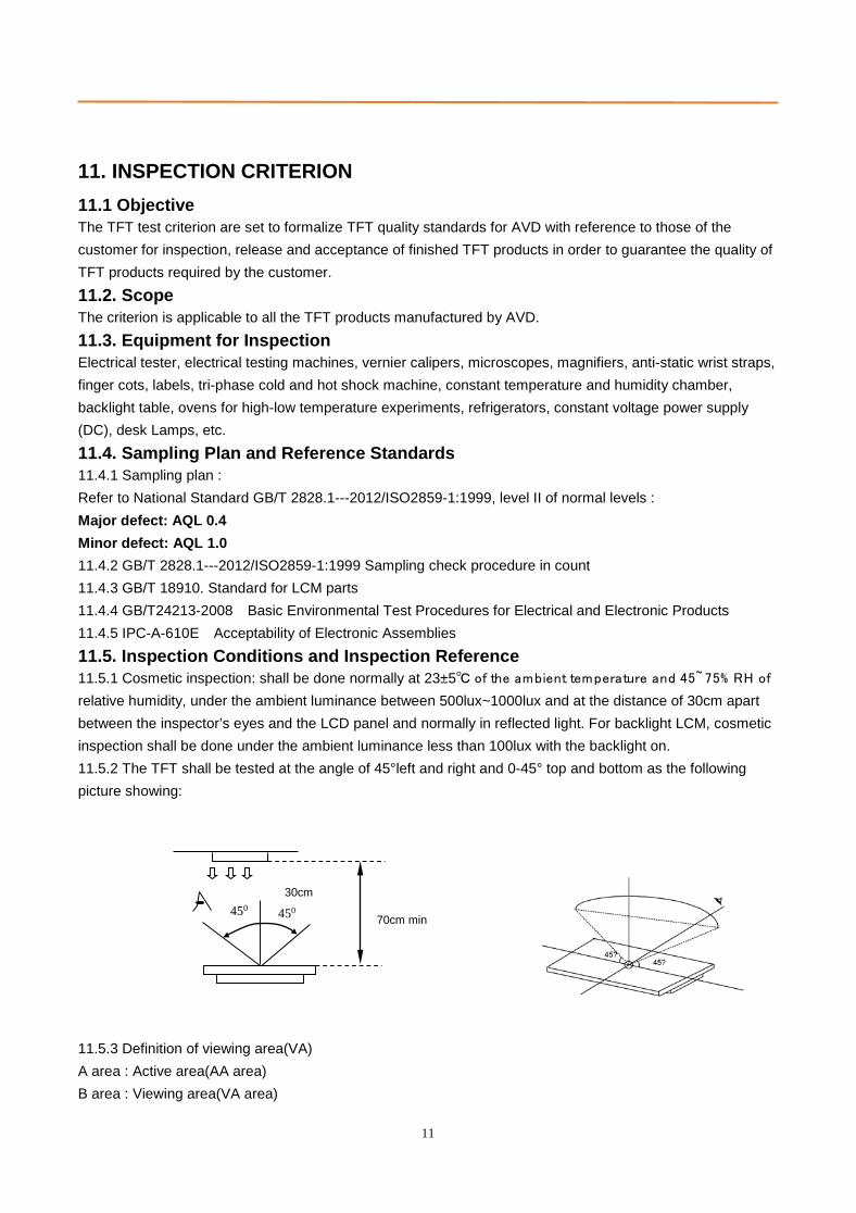
relative humidity, under the ambient luminance between 500lux~1000lux and at the distance of 30cm apart between the inspector’s eyes and the LCD panel and normally in reflected light. For backlight LCM, cosmetic inspection shall be done under the ambient luminance less than 100lux with the backlight on. 11.5.2 The TFT shall be tested at the angle of 45°left and right and 0-45° top and bottom as the following picture showing:
11.5.3 Definition of viewing area(VA) A area : Active area(AA area) B area : Viewing area(VA area)
450 450 70cm min
30cm

12
C area : Non-viewing area(not viewing after customer assembly) If there is any appearance viewing defect which do not affect product quality and customer assembly in C area, it’s accepted in generally. The criteria apply to A and B area except chipping and crack.
11.5.4 Inspection with naked eyes(exclusive of the inspection of the physical dimensions of defects carried out with magnifiers) 11.5.5 ND card use method(refer to right conner image) and scope: Multi-bright dot; Mura(Black/Gray pattern uneven); dark line and so on. 11.5.6 Undefined items or other special items, refer to mutual agreement and limited sample.If criterion does not match product specifications/ technical requirement, both should be subject to special inspection criterion agreed by customer. 11.6. Defects and Acceptance Standards 11.6.1 Electrical properties test 11.6.1.1 Test voltage(V) : Refer to the instruction of testers and the product specification or drawing and the display content and parameters and display effects shall conform to the product specification and drawing. 11.6.1.2 Current Consumption(I) : Refer to approved product specifications or drawings. 11.6.1.3 Function items(Defect category : MA.)
No. Defects Descriptions Pictures Inspection
method/tools Defect
category
11.6.1.3.1 No display
/reaction
shows no picture/display in
normal connected situation.
Naked eyes/
testers MA.
11.6.1.3.2 Missing
segment
Shows missing lines in normal
display
Naked eyes/
testers MA.
11.6.1.3.3 Dark line
Only visible on gray pattern, 1 or
more vertical/horizontal
lines:5%ND,not visible,OK
/ Naked eyes/
testers MA.
11.6.1.3.4 POL angle
defect Not accepted
Naked eyes/
testers MA.

13
11.6.1.3.5
Image
retention
(sticking)
Chess pattern stays for 30mins
and change to 50% gray
pattern,disappear time <10s,
OK; if time>10s, NG
Naked eyes/
testers MA.
11.6.1.3.6 Flicker
Refer to limit sample if essential
or flicker value<-30dB(measured
by CA310A); OK
Naked eyes/
CA310A MA.
11.6.1.3.7 Display
abnormal Not accepted
Naked eyes/
testers MA.
11.6.1.3.8 Cross-talk Refer to limited sample Naked eyes/
limited sample MA.
11.6.1.3.9 Display
dim/bright Refer to limited sample /
Naked eyes/
limited sample MA.
11.6.1.3.10 Contrast Refer to limited sample / Naked eyes/
limited sample MA.
11.6.1.3.11 Huge
current Out of spec, not accepted / Ammeter MA.
11.6.1.3.12 TP function
defect Not accepted /
Naked eyes/
Touch/
test program
MA.
11.6.2 LCD dot/line defect 11.6.2.1 LCD pixel dot defect(defect category : MI.)
Item Inspection criterion
Size S<5” 5’’≤S<10” 10’’≤S<15”
Color pixel dot defect(RGB dot) 1 2 2
2 connected bright dot 0 1 1
3 connected bright dot or more 0 0 1
Bright dot quantity 1 2 3
Random dark dot quantity 2 3 4
2 connected dark dot 1 1 2
3 connected dark dot or more 0 0 0
Dark dot quantity 3 4 5

14
Item Inspection criterion
Multi-bright dot ND 3%hidden, OK
Remark: 2 bright dots distance DS≥15mm 2 dark dots distance DS≥5mm
1) Bright dot: Power on TFT and RGB dot in black display
2) Dark dot: Power on TFT and gray or black dot in RGB display
3) Multi-bright dot: Power on TFT and fluorescent tiny dot in black display(only visible in black display)
11.6.2.2 LCD appearance dot defect (defect category : MI.)
No. Item Inspection criterion
Picture Inspection
method/tools Size S<5” 5’’≤S<10” 10’’≤S<15”
11.6.2.2.1
Dot defect
(black dot,
white dot)
D≤0.15 Not count Not count D≤0.2mm
Not count
D=(a+b)/2
Naked eyes
/film card
/magnifier
0.15<D≤0.25 3 3
0.25<D≤0.30 1 2 0.2~0.35mm
Q’ty ≤ 4 0.30<D≤0.35 0 1
0.35<D≤0.50 0 0 1
D>0.5 0 0 0
Remark : D≤0.15mm, not count.Multi-dot as bulk is not accepted.
Count dot quantity≤ 5
2 round dots or linear dots in 1 cm is judged as multi-dot.
11.6.2.2.2
Line defect
(visible
when
power on)
Length
(mm)
Width
(mm) S<5” 5’’≤S<10” 10’’≤S<15”
Naked eyes
/film card
/magnifier
Not
count W≤0.03 Accepted Accepted Accepted
L≤5 0.03≤W
<0.05 3 3 Not count
L≤5 0.05≤W
<0.08 0 1 3
L≤8 0.05≤W
<0.08 0 0 1
L>8 W>0.08 0
Remark :
Invisible when power on,only visible in special angle against light, show as
watermark/folding/scratch but can not be touched, no control or refer to keeping
sample.
11.6.2.2.3 Size(mm) S<5” 5’’≤S<10” 10’’≤S<15” Naked eyes

15
Polarizer
convex-
concave
dot defect,
polarizer
bubble
defect
D≤0.20 Not count Not count Not count /film card
/magnifier 0.20<D≤0.5 2 2 3
0.50<D≤0.8 0 1
0.8<D≤1.5 0 0 1
D>1.5mm 0 0 0
11.6.3 Chipping defect
No. Item Accepted criterion(mm) MA. MI.
11.6.3.1 ITO conductive side X / ≤1/8L /
√ Y Y≤1/6W 1/6W <Y≤1/4W 1/4W <Y
Accept 2 2 0
11.6.3.2
Corner chipping
(ITO pins position)
X / ≤1/6L / √
Y Y≤1/2W 1/2W <Y≤W W <Y
Accept 2 1 0
Corner chipping occurred in sealed edge position as per 6.3.3; at the same time it should not enter into black border of the frame and the corner chipping effect the electric connection position perform as per 6.3.1.
11.6.3.3
Chipping in sealed area (outside chipping)
X / ≤1/8L /
√
Y(outside chipping) Not enter
into sealant
Enter Y≤H
H<Y
Y(inside chipping)
Enter Y≤1/2H
1/2H<Y
Z ≤T ≤1/2T /
Accept 2 1 0
The standards of inner and outer chipping on edge sealing area are same. When the chipping occurred in the opposite of stage, Y as per the chipping on the non-conduction side standard in 6.3.1

16
Chipping in sealed area (inside chipping)
11.6.3.4
Conductive side (back side chipping)
X / ≤1/6L /
√ Y Y≤1/3W 1/3W <Y≤2/3W 2/3W <Y
Accept 2 2 0
Chipping into ITO side, refer to 6.3.1
11.6.3.5
Protruding LCD poor cutting and LCD burrs
X / ≤1/8L /
√ Y ≤1/6W 1/6W <Y≤1/5W 1/5W <Y
Z / / /
Accept 1 1 1
The outside protruding control as per the tolerance of drawing.
11.6.3.6
Crack Not allow to occur cracks without direction; the crack expand to inside is NG, but to outside is OK (confirmed as per the damaged standard)
√
Remark :
X means the length of chipping;
Y means the width;
Z means the thickness;
W means the step width of the two glasses;
H means the distance from the glass edge to the sealant inner edge;
T means glass thickness.
11.6.4 Backlight components
No. Item Description Accepted criterion MA. MI.
11.6.4.1 No backlight wrong Color
/ Rejected √
11.6.4.2 Color
deviation
When powered on, the LCD color differs from its sample and found that the color not conforming to the drawing after testing.
Refer to sample and drawing
√
b
w
x
z
y

17
11.6.4.3 Brightness deviation
When powered on, the LCD brightness differs from its sample and is found after testing not conforming to the drawing; or if it conforms to the drawing but the brightness over ±40% than its typical value.
Refer to sample and drawing
√
11.6.4.4 Uneven
brightness
Uneven on the same LCD and out of the specification of the drawing. The no specification evenness= (the max value-the min value)/ mean value< 70%.
Refer to sample and drawing
√
11.6.4.5 Spot/line/ scratch
When power on, it has dirty spot, scratches and so on spot and line defects.
Refer to 6.2.2 √
11.6.5 Metal frame (Metal Bezel) No. Item Description Accepted criterion MA. MI.
11.6.5.1 Material &
surface treatment
Metal frame/surface treatment do not conform to the specifications.
Rejected √
11.6.5.2
Tab twist Unconformity/
Tab not twisted
Wrong twist method or direction and twist tabs are not twisted as required.
Rejected √
11.6.5.3 Bezel paint
loss 1.Front surface : Paint peel off and scratch to the bottom Dot:D≤0.5mm, exceeds 3; Line:L≤3.0mm,W≤0.05mm exceeds 2; 2.Front dent, air bubble and side with paint peeling off scratch to the bottom Dot: D≤1.0mm, exceeds 3; Line:L≤3.0mm,W≤0.05mm, exceeds 2;
Rejected
√
11.6.5.4 Bezel scratch √
11.6.5.5
Painting peel
off,
discoloration,
dent, and
scratch
√
11.6.5.6 Burr Burr(s) on metal bezel is so long as to get into viewing area.
Rejected √
11.6.6 FPC
No. Item Description Accepted criterion MA. MI.
11.6.6.1 Model &P/N Material model & P/N Keep the same with drawing and technical requirement
√

18
11.6.6.2 Dimension/ position
Dimension in drawing spec
Remark: H=ITO pin length f=FPC width W=ITO pin width
f≤1/3w, h ≤1/3H, dimension in drawing spec-> OK Conducive material and ITO/PDA connective area must over than 1/2. Entire dimension must be in spec tolerance.
√
11.6.6.3 FPC appearance
Hot pressing material get broken, folding line open; FPC golden finger oxidate, broken ,scratch ,foreign material which cause line short
Broken length<2mm; FPC line is OK- > Accepted Crack and line broken->Rejected
√
11.6.6.4 FPC burr Burr near FPC edge area When cover line and burr length ≤1.0mm->Accepted
√
11.6.6.5 FPC falling off
FPC bonding area falling off ; silica gel breaking
Rejected √
11.6.6.6 Sealant missing ITO line
Sealant is not covered all ITO line Rejected √
11.6.6.7 Missing sealant
No sealant Rejected √
11.6.6.8 Sealant Sealant height ->product total height Rejected √
11.6.7 SMT
No. Item Description Accepted criterion MA. MI.
11.6.7.1 Soldering
bridge
Solder between adjacent pads and components
Rejected √
11.6.7.2 Solder
ball/splash
Solder ball/tin dross causing short circuit at the solder point. There are active solder ball and splash.
Rejected √
f w
h
H
X
h2
Hh1

19
11.6.7.3 Soldering excursion
Soldering slant > 1/3 soldering pad
Rejected √
11.6.7.4 Component wrong attaching
Component on PCB differs with drawing: wrong one, extra one,lack one,opposite polarity
Rejected √
JUMP short circuit on PCB: extra soldering ,lack soldering.
Rejected √
11.6.7.5 Component falling off
Soldering but component is missing
Rejected √
11.6.7.6 Wrong component
Component model/spec differs from product specification
Rejected √
11.6.8 General Appearance
No. Item Description Accepted criterion MA. MI.
11.6.8.1 Dimension According to drawing Accepted √
11.6.8.2 Surface
stain Defect mark or label are not removed residual glue, and finger print,etc;
Rejected √
11.6.8.3 Assembly
foreign material
Dot/linear stain after assembly backlight and diffuse film TP assembly fogy stain
Invisible when power on->OK Refer to 6.2.2 dot/line spec
√
11.6.8.4 Mixture Different model product in the same shipment
Rejected √
11.6.8.5 Product
mark Missing, unclear, incorrect, or misplaced part
Rejected √
11.6.8.6 Component
mark Silk screen mark clear, resistance measured value in spec
Accepted (Refer to customer special requirement)
√
11.6.8.7 Newton’s
rings Area<1/6 screen area quantity≤1 Accepted √
11.6.8.8 Mura
1.In black display
ND 3% invisible ->OK; visible->NG
2.Naked eyes inspection
RGB display invisible
Black display, area<1/4 screen area
Refer to limited sample
√

20
11.6.8.9 Light leak
1.LCD edge(near backlight) shadow
by LCD lamps irregular illuminate
2.Judge in black/white/gray display
(slight leaky is yellowish,greenish,
blueish ->NG); Refer to limited sample √
11.6.8.10 Polarizer
1.Polarizer slant.Cover VA and not over
LCD edge
2.No unmovable stain or finger print in
polarizer VA
3.Bubble/warped but not enter VA
Accepted √
11.6.8.11 TP defect
1.TP crack
2.TP stain(fogy& unremovable)
3.TP glue overflow to VA
Rejected √
Remark : Anything which is not clearly defined in 6.5~6.8 should refer to IPC-A-610E.Consumer Electronics, Non-consumer Electronics refer toⅠgrade and Industrial,Automobile refer to Ⅱgrade. 11.7 Others Items not specified in this document or released on compromise should be inspected with reference to mutual agreement and limit samples.