Embed Size (px)
Citation preview
2014/6/25
Current and future of analogand RF circuits technology
Akira Matsuzawa
Tokyo Institute of Technology
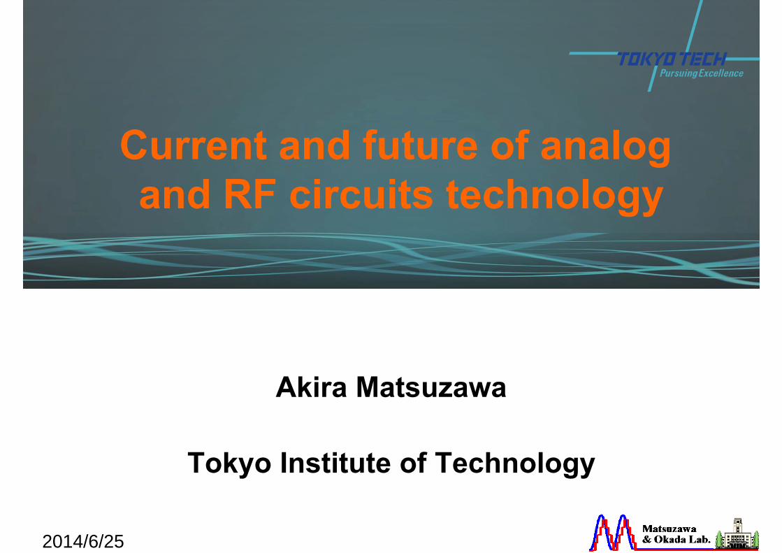
1Contents
2014/6/25
• RF circuits– Challenge for ultra-high speed data transfer using millimeter
wave technology• 60GHz CMOS transceiver attained 28Gbps• Toward 300Gbps
• ADC– Performance trend– Scalable12bit SAR ADC– 7bit 2.2GHz ADC using time-domain signal processing
• PLL• Layout-driven circuit design and programmable analog
circuit technique • Summary
懇話会 6月 松澤
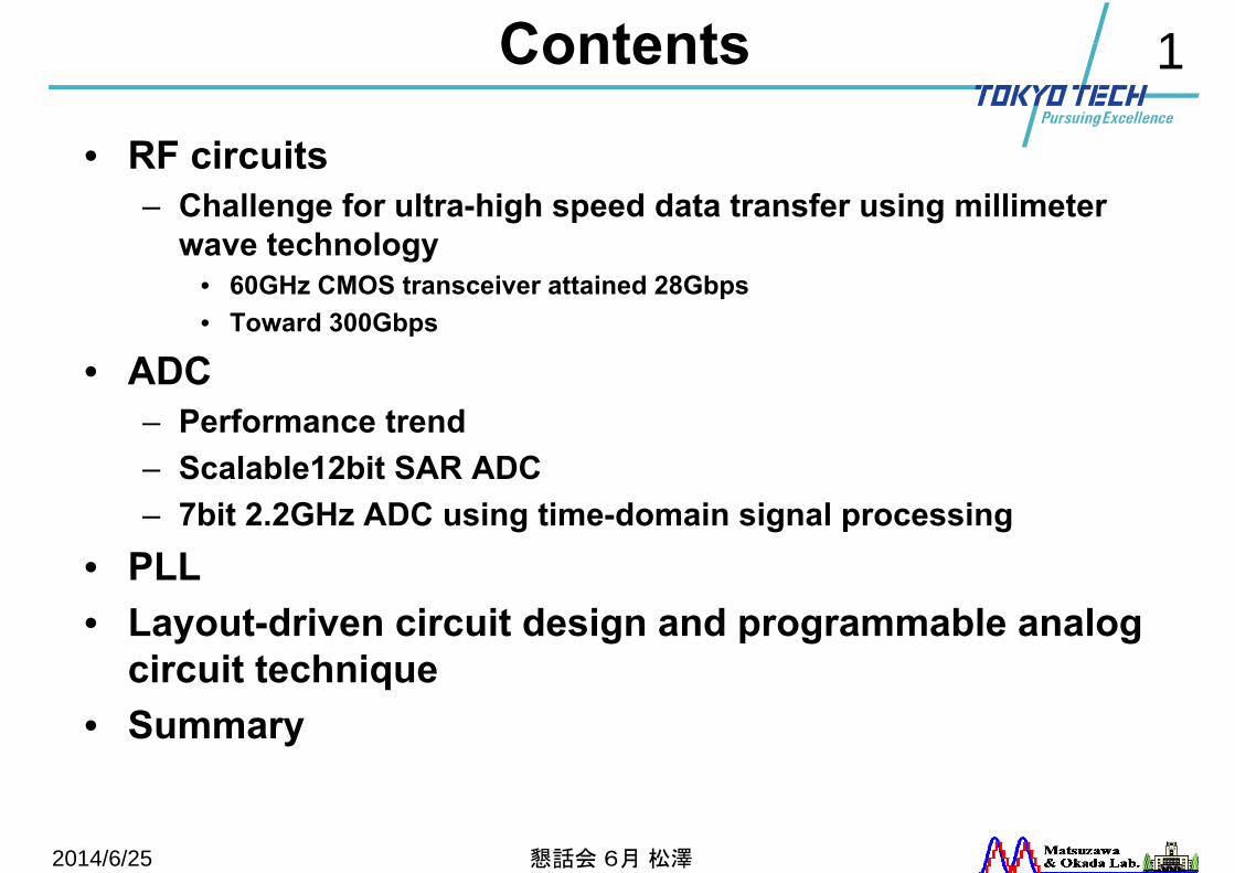
2Analog & RF circuits
2014/6/25
Low power
Wide BWHigh SNDR
・Dynamic circuits・Charge base・Low energy loss
・Small cap.
・Low noise・Low jitter・Low distortion・Linearization・High power
N
S
PPBWC 1log2
Data rate∝BW×SNR(dB)
Shannon’s theorem
懇話会 6月 松澤
・Scaled transistor・Frequency compensation・Distributed circuit
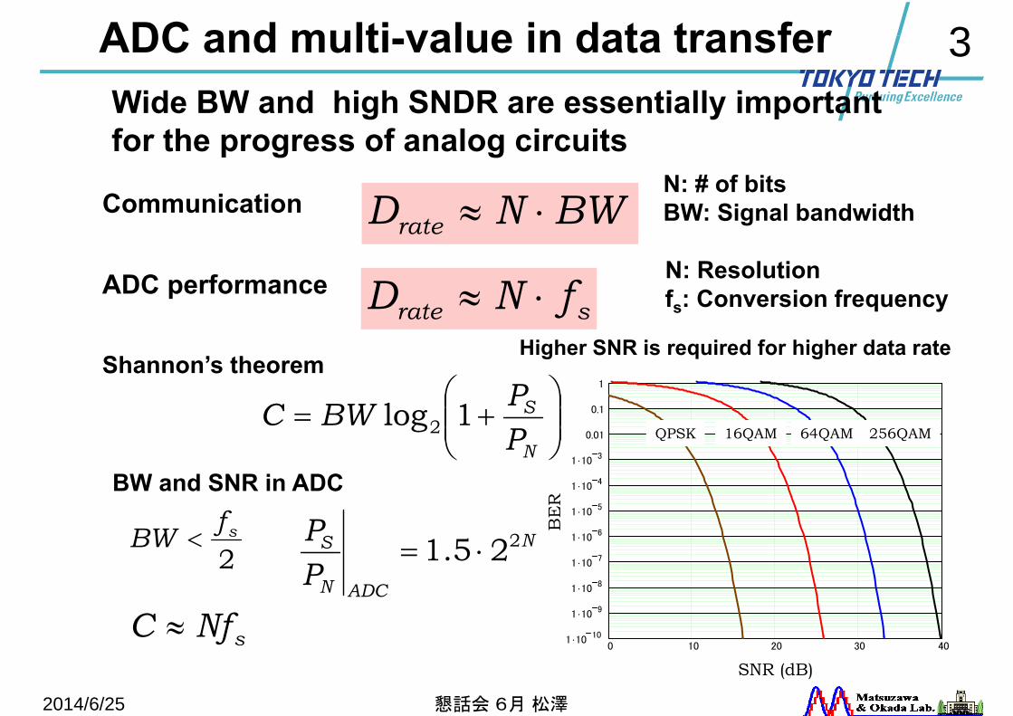
3ADC and multi-value in data transfer
0 10 20 30 401 10 10
1 10 9
1 10 8
1 107
1 106
1 105
1 104
1 103
0.01
0.1
1
6)
SNR (dB)
BE
R
QPSK 16QAM 64QAM 256QAM
N
S
PPBWC 1log2
N
ADCN
S
PP 225.1
BW and SNR in ADC
sNfC
BWNDrate
Higher SNR is required for higher data rate
2sfBW
2014/6/25
N: # of bitsBW: Signal bandwidth
srate fND
Communication
ADC performance N: Resolutionfs: Conversion frequency
懇話会 6月 松澤
Wide BW and high SNDR are essentially important for the progress of analog circuits
Shannon’s theorem
4
RF circuits
Challenge for ultra-high speed data transfer using millimeter wave technology
2014/6/25 懇話会 6月 松澤
5
2014/6/25
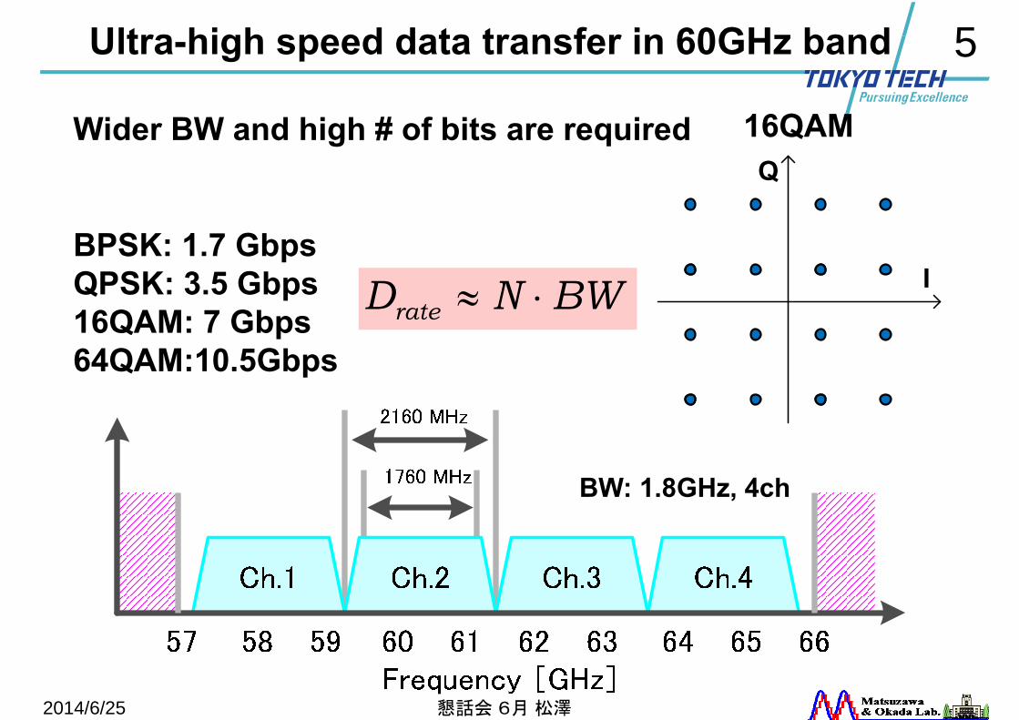
Ultra-high speed data transfer in 60GHz band
BW: 1.8GHz, 4ch
BPSK: 1.7 GbpsQPSK: 3.5 Gbps16QAM: 7 Gbps64QAM:10.5Gbps
I
Q16QAM
BWNDrate
Wider BW and high # of bits are required
懇話会 6月 松澤
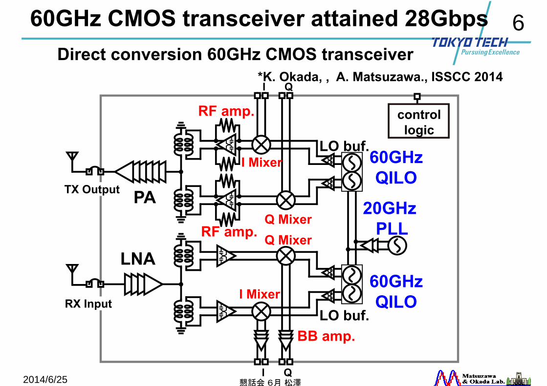
660GHz CMOS transceiver attained 28Gbps
2014/6/25
PA
60GHzQILO
LNA
I Mixer
Q Mixer
LO buf.
RF amp.
I Mixer
Q Mixer
LO buf.60GHzQILO
20GHzPLL
TX Output
I Q
I Q
BB amp.
RX Input
RF amp.
controllogic
*K. Okada, , A. Matsuzawa., ISSCC 2014Direct conversion 60GHz CMOS transceiver
懇話会 6月 松澤
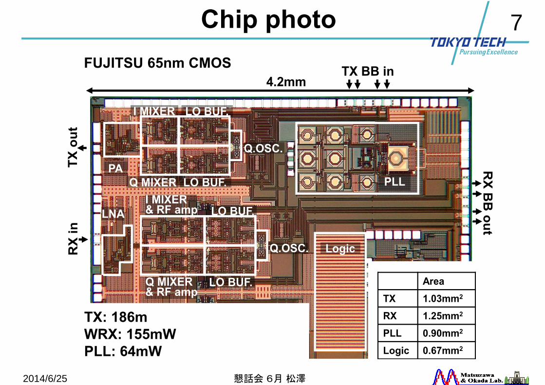
7Chip photo
2014/6/25
PAQ MIXER
I MIXER
LO BUF.
LO BUF.
Q.OSC.
Logic
PLL
LNAI MIXER& RF amp
LO BUF.
LO BUF.
Q.OSC.
RX
BB
outTX
out
RX
inTX BB in
4.2mm
AreaTX 1.03mm2
RX 1.25mm2
PLL 0.90mm2
Logic 0.67mm2
CMOS 65nm, 1Al+11CuTX: 186mWRX: 155mWPLL: 64mW
Q MIXER& RF amp
FUJITSU 65nm CMOS
TX: 186mWRX: 155mWPLL: 64mW
懇話会 6月 松澤
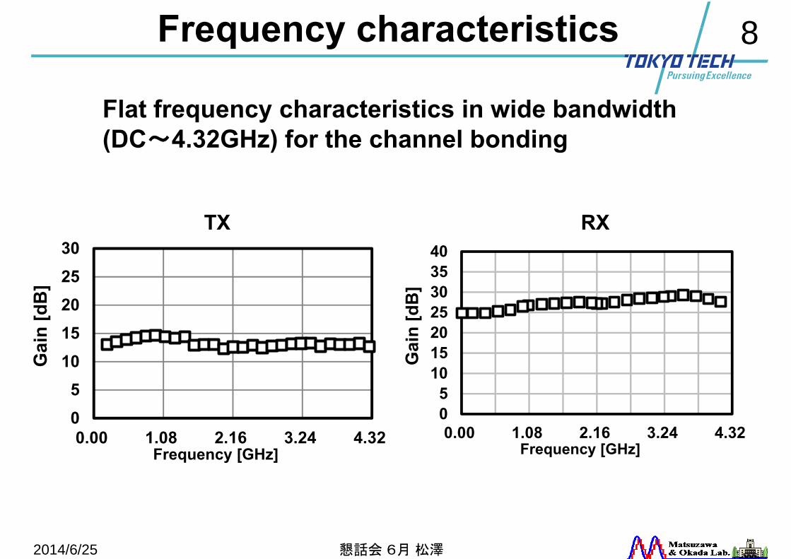
8Frequency characteristics
2014/6/25
Flat frequency characteristics in wide bandwidth (DC~4.32GHz) for the channel bonding
05
1015202530
0.00 1.08 2.16 3.24 4.32
Gai
n [d
B]
Frequency [GHz]
Gai
n [d
B]
Frequency [GHz]
05
10152025303540
0.00 1.08 2.16 3.24 4.32
TX RX
懇話会 6月 松澤
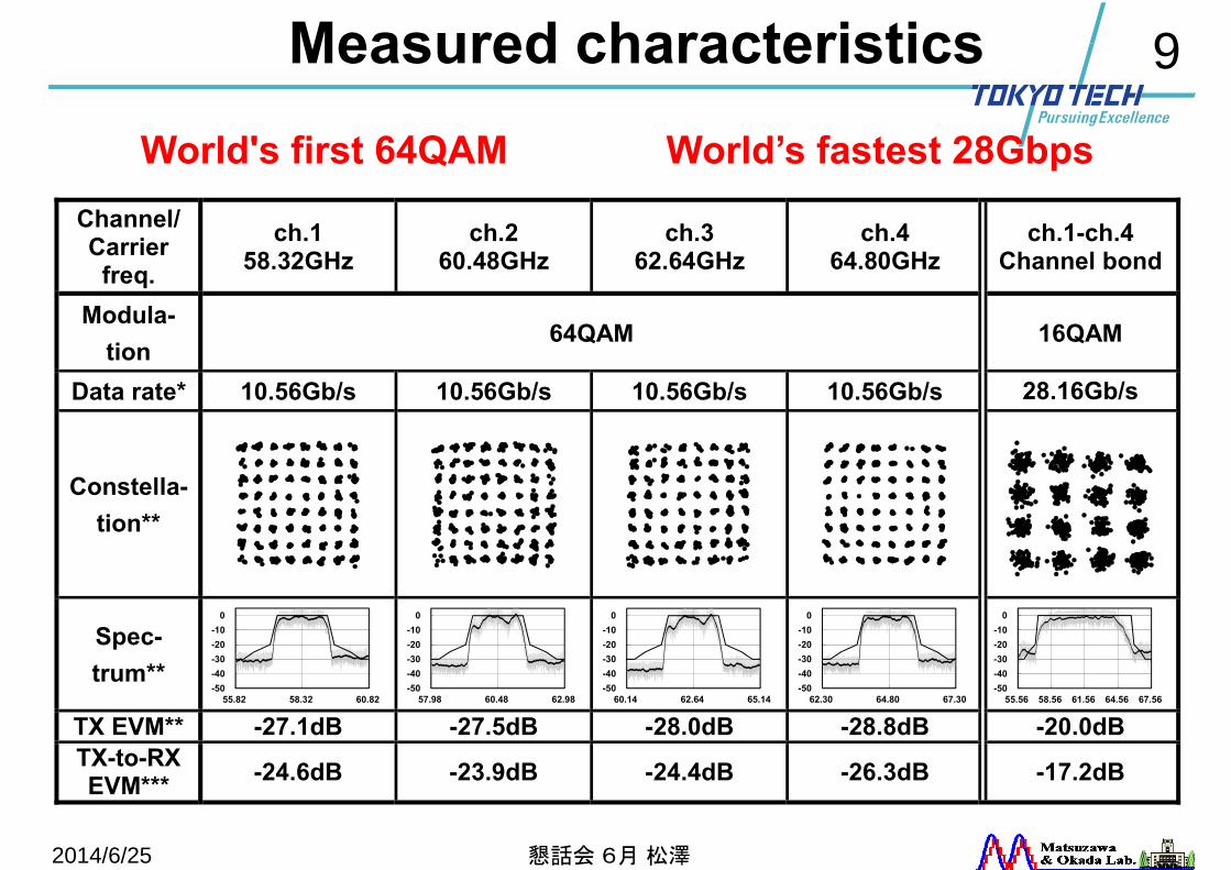
9Measured characteristics
2014/6/25
Channel/Carrier
freq. ch.1
58.32GHz ch.2
60.48GHz ch.3
62.64GHz ch.4
64.80GHz ch.1-ch.4
Channel bond
Modula- tion
64QAM 16QAM
Data rate* 10.56Gb/s 10.56Gb/s 10.56Gb/s 10.56Gb/s 28.16Gb/s
Constella-tion**
Spec- trum**
TX EVM** -27.1dB -27.5dB -28.0dB -28.8dB -20.0dB TX-to-RX EVM*** -24.6dB -23.9dB -24.4dB -26.3dB -17.2dB
-50-40-30-20-10
0
55.82 58.32 60.82-50-40-30-20-10
0
57.98 60.48 62.98-50-40-30-20-10
0
60.14 62.64 65.14-50-40-30-20-10
0
62.30 64.80 67.30-50-40-30-20-10
0
55.56 58.56 61.56 64.56 67.56
World's first 64QAM World’s fastest 28Gbps
懇話会 6月 松澤
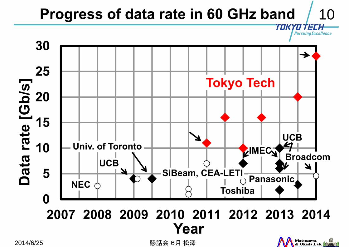
10Progress of data rate in 60 GHz band
2014/6/25
0
5
10
15
20
25
30
2007 2008 2009 2010 2011 2012 2013 2014
Dat
a ra
te [G
b/s]
Year
UCB
NEC
Univ. of Toronto
SiBeam, CEA-LETI
Toshiba
IMEC
Panasonic
UCB
Broadcom
Tokyo Tech
懇話会 6月 松澤
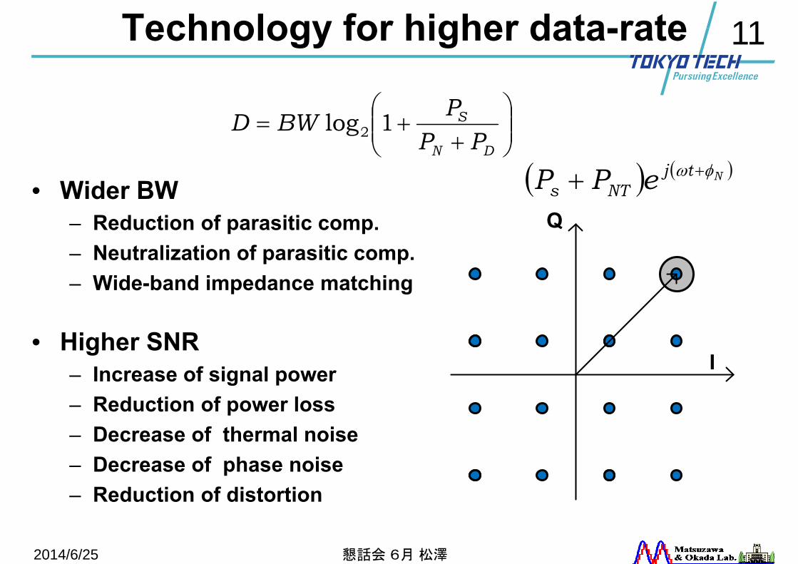
11Technology for higher data-rate
2014/6/25
DN
S
PPPBWD 1log2
I
Q
NtjNTs ePP
懇話会 6月 松澤
• Wider BW– Reduction of parasitic comp.– Neutralization of parasitic comp.– Wide-band impedance matching
• Higher SNR– Increase of signal power– Reduction of power loss– Decrease of thermal noise– Decrease of phase noise– Reduction of distortion
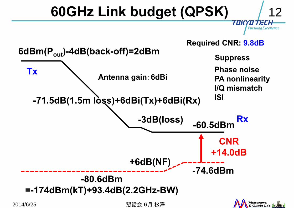
1260GHz Link budget (QPSK)
2014/6/25
6dBm(Pout)-4dB(back-off)=2dBm
-80.6dBm=-174dBm(kT)+93.4dB(2.2GHz-BW)
-74.6dBm+6dB(NF)
-60.5dBm-3dB(loss)
CNR+14.0dB
Tx
Rx
-71.5dB(1.5m loss)+6dBi(Tx)+6dBi(Rx)
Required CNR: 9.8dB
Antenna gain:6dBi
懇話会 6月 松澤
Phase noisePA nonlinearityI/Q mismatchISI
Suppress
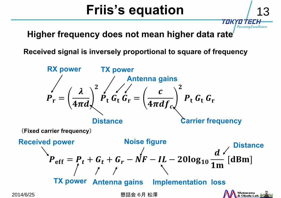
13Friis’s equation
2014/6/25
TX powerAntenna gains
Distance
RX power
Carrier frequency
Received power Noise figure
Implementation lossTX power
(Fixed carrier frequency)
懇話会 6月 松澤
Antenna gains
Distance
Higher frequency does not mean higher data rate
Received signal is inversely proportional to square of frequency
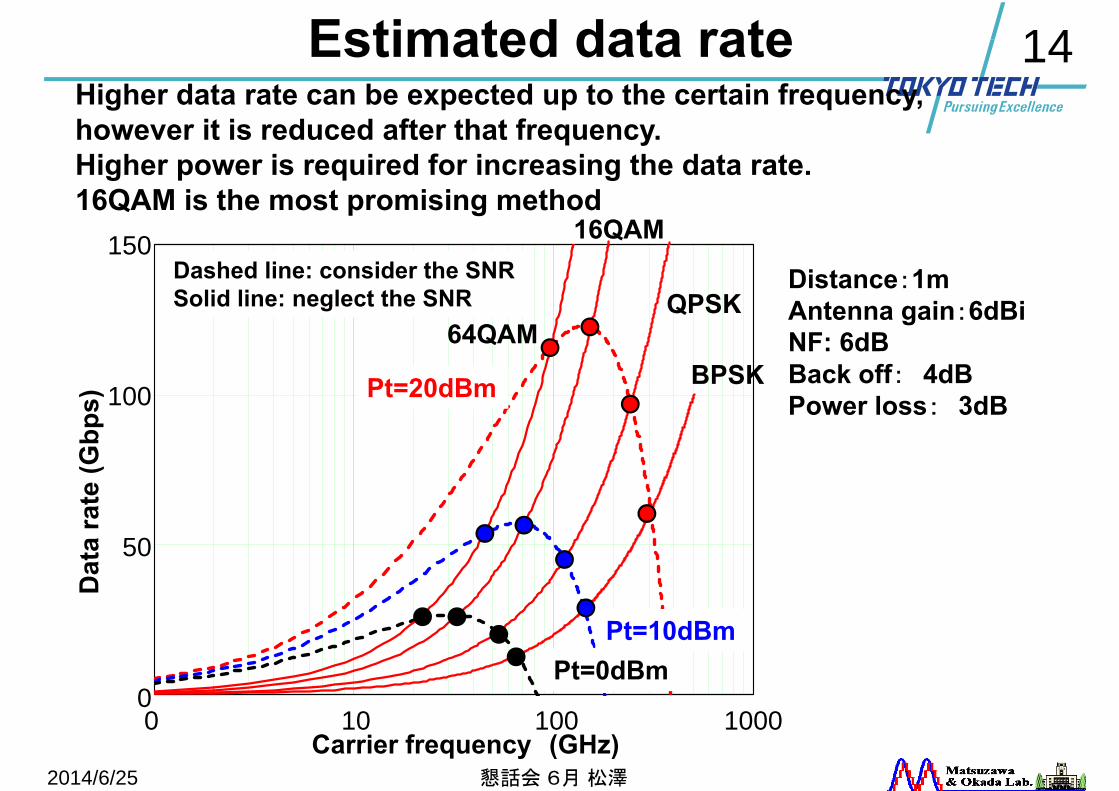
14Estimated data rate
2014/6/25
0
50
100
150
0 10 100 1000
Dat
a ra
te (G
bps)
Carrier frequency (GHz)
Pt=20dBm
Pt=10dBmPt=0dBm
BPSK
QPSK
16QAM
64QAM
Dashed line: consider the SNRSolid line: neglect the SNR
Distance:1mAntenna gain:6dBiNF: 6dBBack off: 4dBPower loss: 3dB
懇話会 6月 松澤
Higher data rate can be expected up to the certain frequency,however it is reduced after that frequency.Higher power is required for increasing the data rate.16QAM is the most promising method
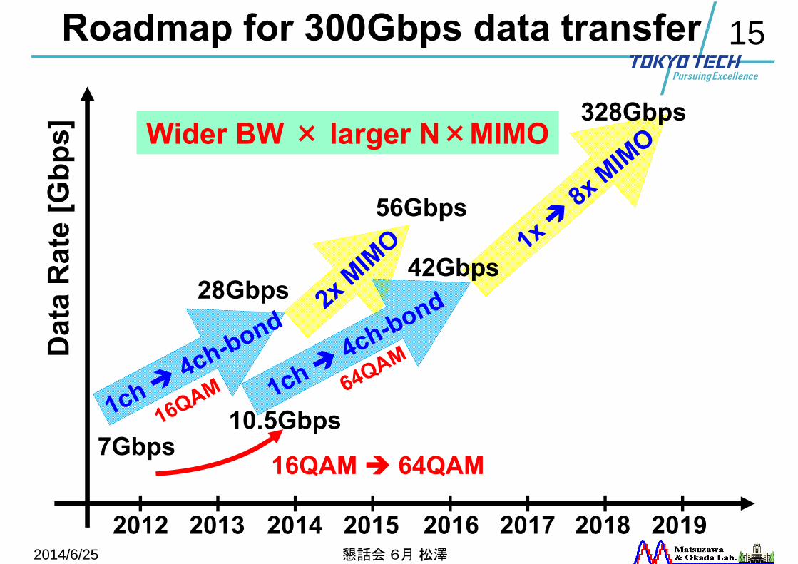
15Roadmap for 300Gbps data transfer
7Gbps
28Gbps
10.5Gbps
2014
16QAM 64QAM
42Gbps
328Gbps
56Gbps
20162012 20182015 20172013 2019
Dat
a R
ate
[Gbp
s] Wider BW × larger N×MIMO
2014/6/25 懇話会 6月 松澤
16
ADC
2014/6/25 懇話会 6月 松澤
Requirement for ADC development is still high.Begin with ADC development and end with it ?
17
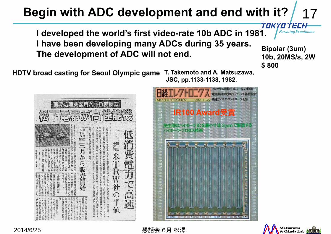
2014/6/25
Begin with ADC development and end with it?
Bipolar (3um)10b, 20MS/s, 2W$ 800
T. Takemoto and A. Matsuzawa,JSC, pp.1133-1138, 1982.
IR100 Award受賞
HDTV broad casting for Seoul Olympic game
懇話会 6月 松澤
I developed the world’s first video-rate 10b ADC in 1981.I have been developing many ADCs during 35 years.The development of ADC will not end.
18
Progress of ADCs
2014/6/25 懇話会 6月 松澤
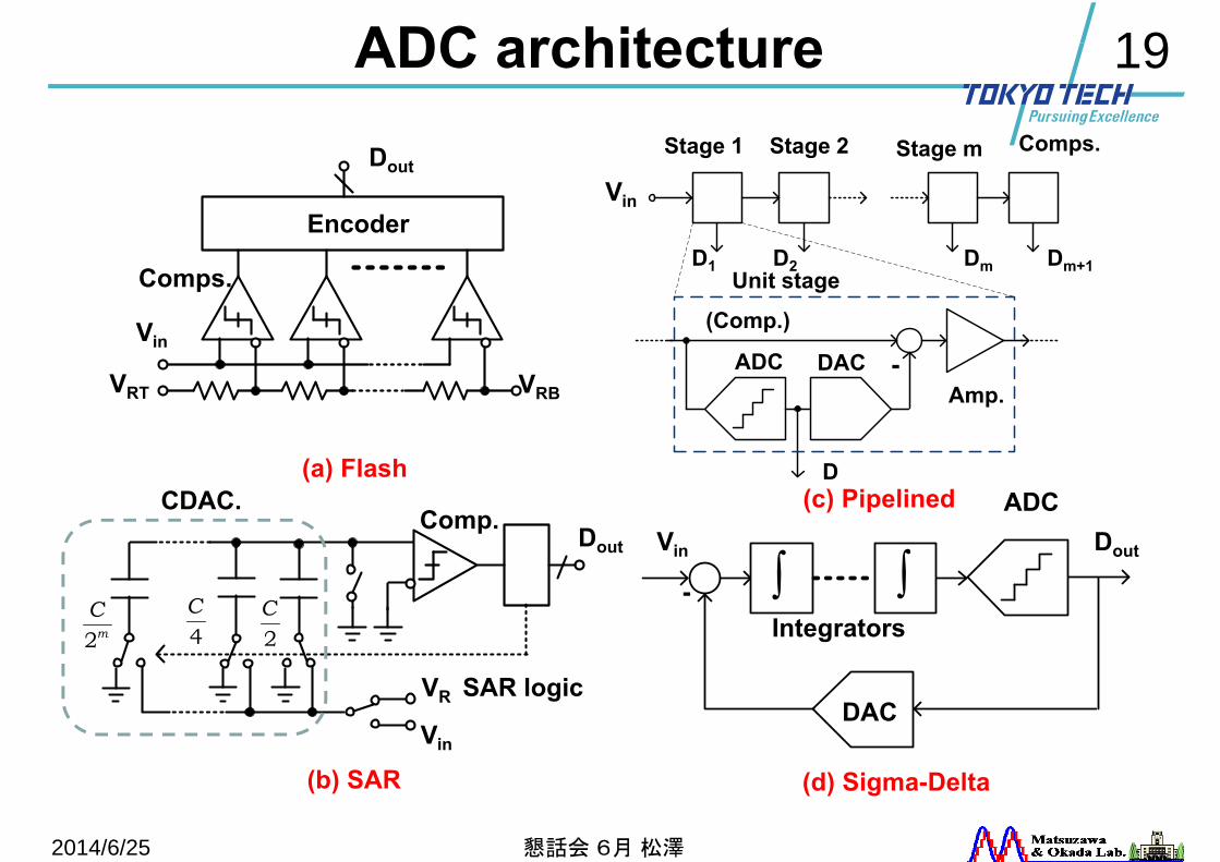
19
Vin
VRT VRB
Comps.
Encoder
Dout
Dout
SAR logic
Comp.
Vin
VR
2C
4C
mC2
CDAC.
ADC
(Comp.)
DACAmp.
-
Vin
D
Stage 1 Stage 2
Unit stage
Stage m Comps.
D1 D2 Dm Dm+1
ADC
DAC
Dout
Vin
-Integrators
(b) SAR
(c) Pipelined
(d) Sigma-Delta
(a) Flash
ADC architecture
2014/6/25 懇話会 6月 松澤
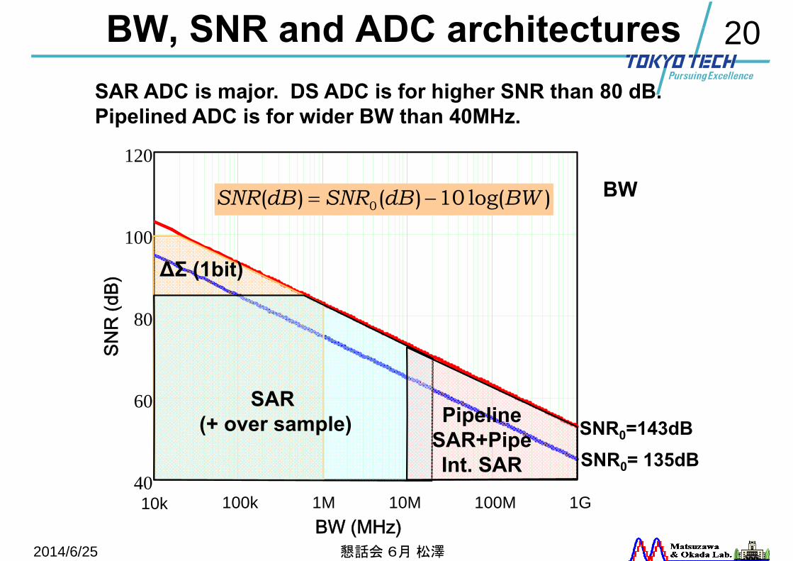
20BW, SNR and ADC architectures
2014/6/25
40
60
80
100
120
SNR0= 135dBSNR0=143dB
BW (MHz)
SNR
(dB)
1G1M10k 100k 10M 100M
SAR (+ over sample)
∆Σ (1bit)
PipelineSAR+PipeInt. SAR
)log(10)()( 0 BWdBSNRdBSNR BW
懇話会 6月 松澤
SAR ADC is major. DS ADC is for higher SNR than 80 dB.Pipelined ADC is for wider BW than 40MHz.
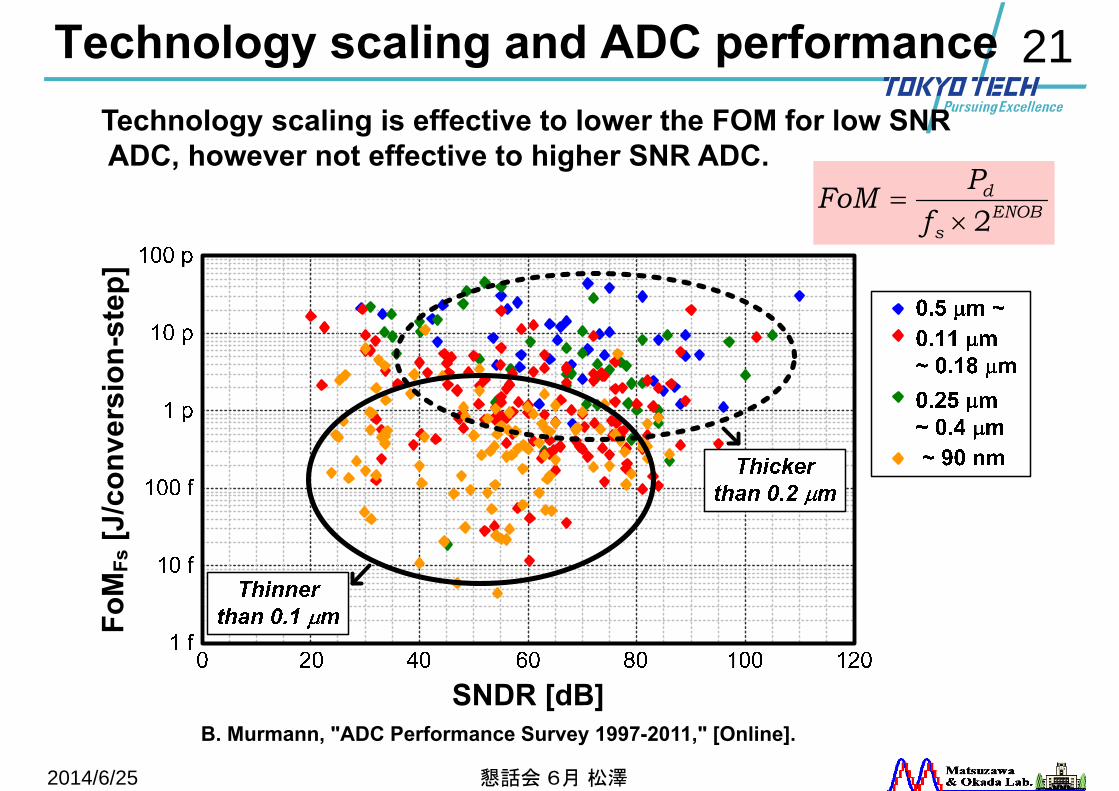
21Technology scaling and ADC performance
2014/6/25
FsTechnology scaling is effective to lower the FOM for low SNRADC, however not effective to higher SNR ADC.
B. Murmann, "ADC Performance Survey 1997-2011," [Online].
懇話会 6月 松澤
ENOBs
d
fPFoM2
22
110
120
130
140
150
160
170
101 102 103
135 (dB/Hz)
143 (dB/Hz)
150 (dB/Hz)
CMOS Node (nm)
SN
R0
(dB
/Hz)
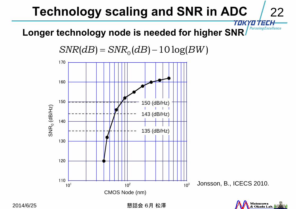
Technology scaling and SNR in ADC
)log(10)()( 0 BWdBSNRdBSNR
Jonsson, B., ICECS 2010.
Longer technology node is needed for higher SNR
2014/6/25 懇話会 6月 松澤
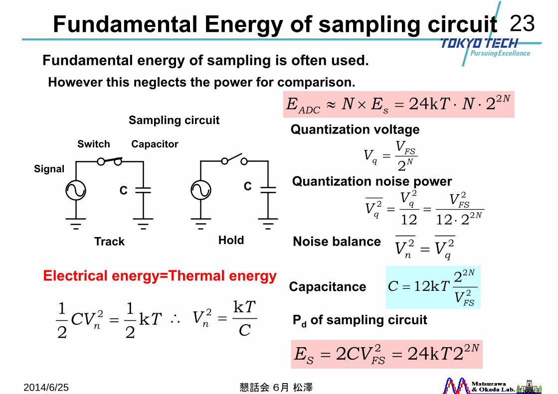
23Fundamental Energy of sampling circuit
Signal
Switch Capacitor
Track Hold
NFSq
qVV
V 2
222
21212
NFS
qVV2
TCVn k21
21 2
Sampling circuit
Electrical energy=Thermal energy
CTVn
k2
Quantization voltage
Quantization noise power
22qn VV
2
22k12FS
N
VTC
C C
NFSS TCVE 22 2242 k
Noise balance
Capacitance
Pd of sampling circuit
NsADC NTENE 2224 k
Fundamental energy of sampling is often used. However this neglects the power for comparison.
2014/6/25 懇話会 6月 松澤
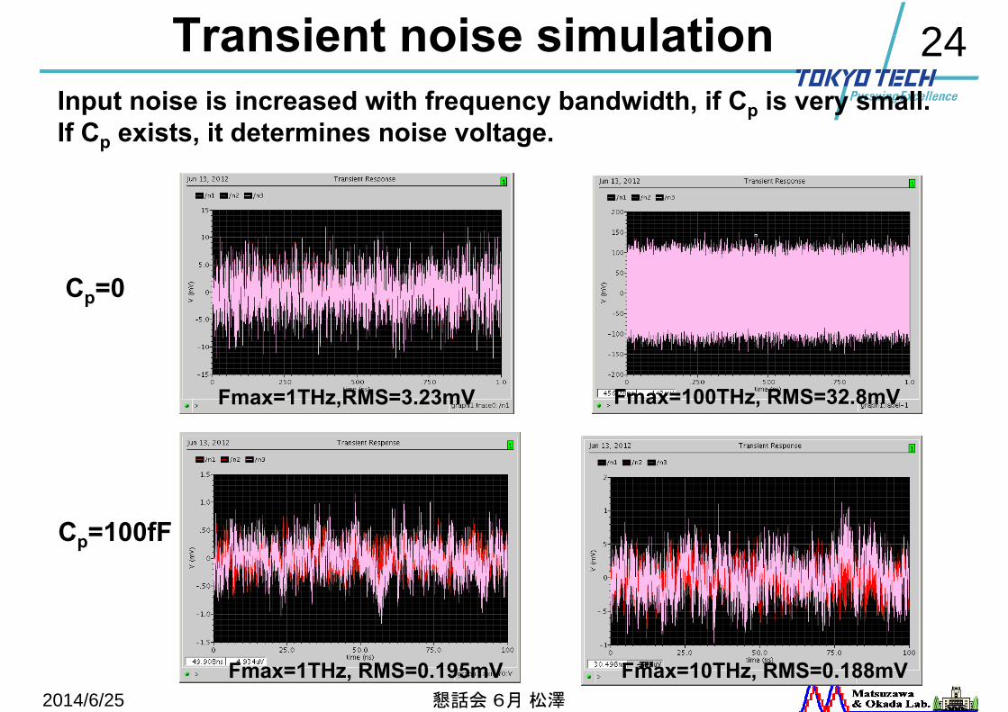
24Transient noise simulation
Fmax=1THz, RMS=0.195mV Fmax=10THz, RMS=0.188mV
Fmax=100THz, RMS=32.8mVFmax=1THz,RMS=3.23mV
Input noise is increased with frequency bandwidth, if Cp is very small.If Cp exists, it determines noise voltage.
Cp=0
Cp=100fF
2014/6/25 懇話会 6月 松澤
25
1.E-01
1.E+00
1.E+01
1.E+02
1.E+03
1.E+04
1.E+05
1.E+06
1.E+07
10 20 30 40 50 60 70 80 90 100 110 120
P/f s
nyq
[pJ]
SNDR @ Nyquist [dB]
ISSCC 2012VLSI 2012ISSCC 1997-2011VLSI 1997-2011FOMW=10fJ/conv-stepFOMS=170dB
Pd/fs and SNDR
Current boundary
Theoretical limit
192 102 NADC NE
P/fs is proportional to SNDR theoretically
2014/6/25 懇話会 6月 松澤
Theoretical limit
26
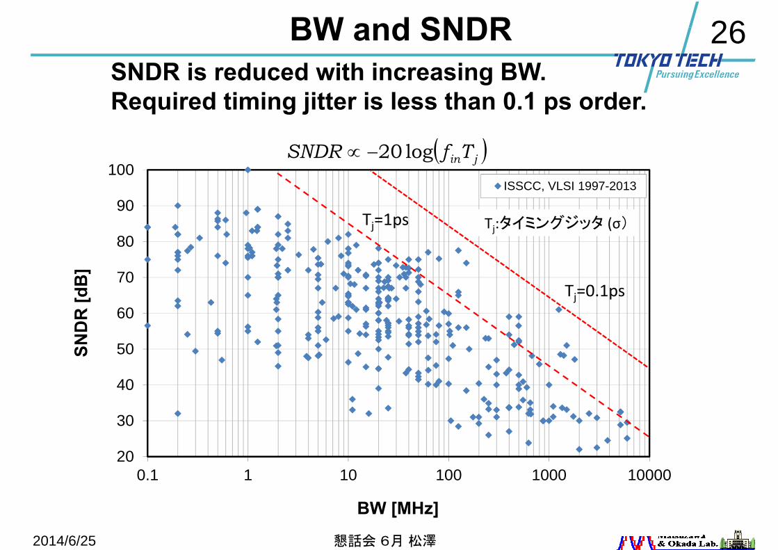
20
30
40
50
60
70
80
90
100
0.1 1 10 100 1000 10000
SND
R[d
B]
BW [MHz]
ISSCC, VLSI 1997-2013
Tj=0.1ps
Tj=1ps Tj:タイミングジッタ (σ)
BW and SNDRSNDR is reduced with increasing BW.Required timing jitter is less than 0.1 ps order.
jinTfSNDR log20
2014/6/25 懇話会 6月 松澤
27
Scalable 12bit SAR ADC
2014/6/25 懇話会 6月 松澤
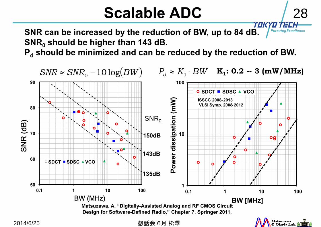
28
2014/6/25
Scalable ADC
50
60
70
80
90
0.1 1 10 100
SDCT SDSC VCO
135dB
143dB
150dB
BW (MHz)
SNR
(dB)
BWSNRSNR log100
)log(10140)( BWdBSNR
sd fP
1
10
100
0.1 1 10 100
BW [MHz]
SDCT SDSC VCOISSCC 2008-2013VLSI Symp. 2008-2012
Pow
er d
issi
patio
n (m
W)
BWKPd 1 K1: 0.2 -- 3 (mW/MHz)
Matsuzawa, A. “Digitally-Assisted Analog and RF CMOS Circuit Design for Software-Defined Radio,” Chapter 7, Springer 2011.
SNR can be increased by the reduction of BW, up to 84 dB.SNR0 should be higher than 143 dB.Pd should be minimized and can be reduced by the reduction of BW.
SNR0
懇話会 6月 松澤
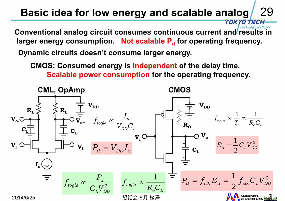
29Basic idea for low energy and scalable analog
LDD
stogle CV
If
CML, OpAmp
VDD
Vi+ Vi-
Vo-
CL
RL
CL
RL
Vo+
Is
RO
CL
ViVo
VDD
CMOS
2DDL
dtogle VC
Pf
Conventional analog circuit consumes continuous current and results inlarger energy consumption. Not scalable Pd for operating frequency.Dynamic circuits doesn’t consume larger energy.
2
21
DDLd VCE
CMOS: Consumed energy is independent of the delay time.Scalable power consumption for the operating frequency.
Lortogle CRTf 11
Lotogle CRf 1
2
21
DDLclkdclkd VCfEfP
sDDd IVP
2014/6/25 懇話会 6月 松澤
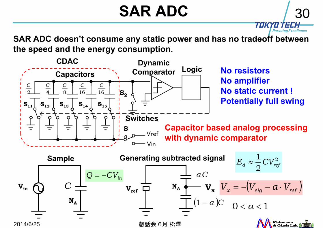
30SAR ADC
Vin
Vref
DynamicComparator Logic
Switches
Capacitors
S11 S12 S13 S14 S15
S2
S0
2C
4C
8C
16C
16C
VrefVin
NA
C
Cα1
Cα
10 α
refsigx VαVV VxNA
Sample 2
21
refd CVE
SAR ADC doesn’t consume any static power and has no tradeoff between the speed and the energy consumption.
Generating subtracted signal
No resistorsNo amplifierNo static current !Potentially full swing
inCVQ
CDAC
Capacitor based analog processingwith dynamic comparator
2014/6/25 懇話会 6月 松澤
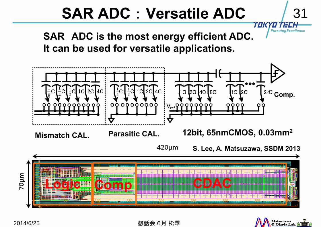
31SAR ADC:Versatile ADC
12
14
18
12
14 Comp.
2014/6/25
SAR ADC is the most energy efficient ADC.It can be used for versatile applications.
Logic Comp CDAC
12bit, 65nmCMOS, 0.03mm2
S. Lee, A. Matsuzawa, SSDM 2013
Parasitic CAL.Mismatch CAL.
懇話会 6月 松澤
32
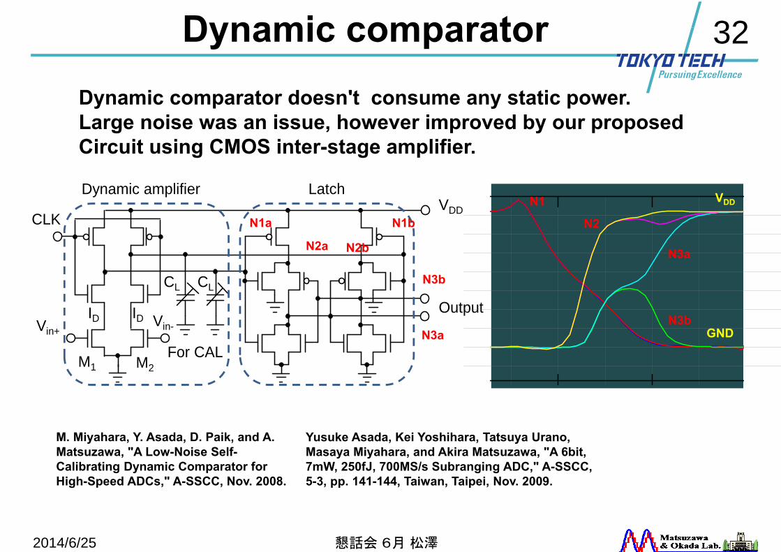
Output
VDDCLK
Vin+
For CAL
Vin-
M1 M2
CL CL
ID ID
Dynamic amplifier Latch
Dynamic comparator
N1a N1b
N2a N2b
N3a
N3b
N2
N1
N3a
N3b
VDD
GND
M. Miyahara, Y. Asada, D. Paik, and A. Matsuzawa, "A Low-Noise Self-Calibrating Dynamic Comparator for High-Speed ADCs," A-SSCC, Nov. 2008.
Yusuke Asada, Kei Yoshihara, Tatsuya Urano, Masaya Miyahara, and Akira Matsuzawa, "A 6bit, 7mW, 250fJ, 700MS/s Subranging ADC," A-SSCC, 5-3, pp. 141-144, Taiwan, Taipei, Nov. 2009.
2014/6/25 懇話会 6月 松澤
Dynamic comparator doesn't consume any static power.Large noise was an issue, however improved by our proposedCircuit using CMOS inter-stage amplifier.
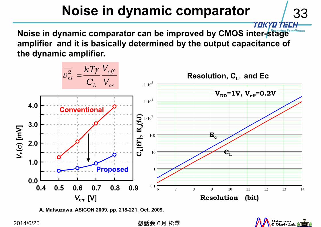
33Noise in dynamic comparator
6 7 8 9 10 11 12 13 140.1
1
10
100
1 103
1 104
1 105
CL(
fF),
Ec(
fJ)
Resolution (bit)
CL
Ec
VDD=1V, Veff=0.2V
V n
Resolution, CL,and Ec
2014/6/25
os
eff
Lni V
VCkTv
2
A. Matsuzawa, ASICON 2009, pp. 218-221, Oct. 2009.
懇話会 6月 松澤
Noise in dynamic comparator can be improved by CMOS inter-stageamplifier and it is basically determined by the output capacitance ofthe dynamic amplifier.
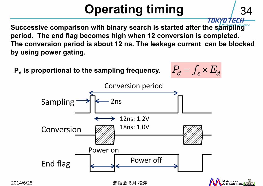
34Operating timing
2014/6/25
Sampling
Power off
Conversion period
Conversion
End flag
Power on
2ns
12ns: 1.2V18ns: 1.0V
dsd EfP Pd is proportional to the sampling frequency.
懇話会 6月 松澤
Successive comparison with binary search is started after the samplingperiod. The end flag becomes high when 12 conversion is completed.The conversion period is about 12 ns. The leakage current can be blockedby using power gating.
35
0.5
0.6
0.7
0.8
0.91
2
3
50 60 70 80 90 100 200
MOM capacitor
MIM capacitor
Design rule (nm)
Den
sity
(fF/
um2 )
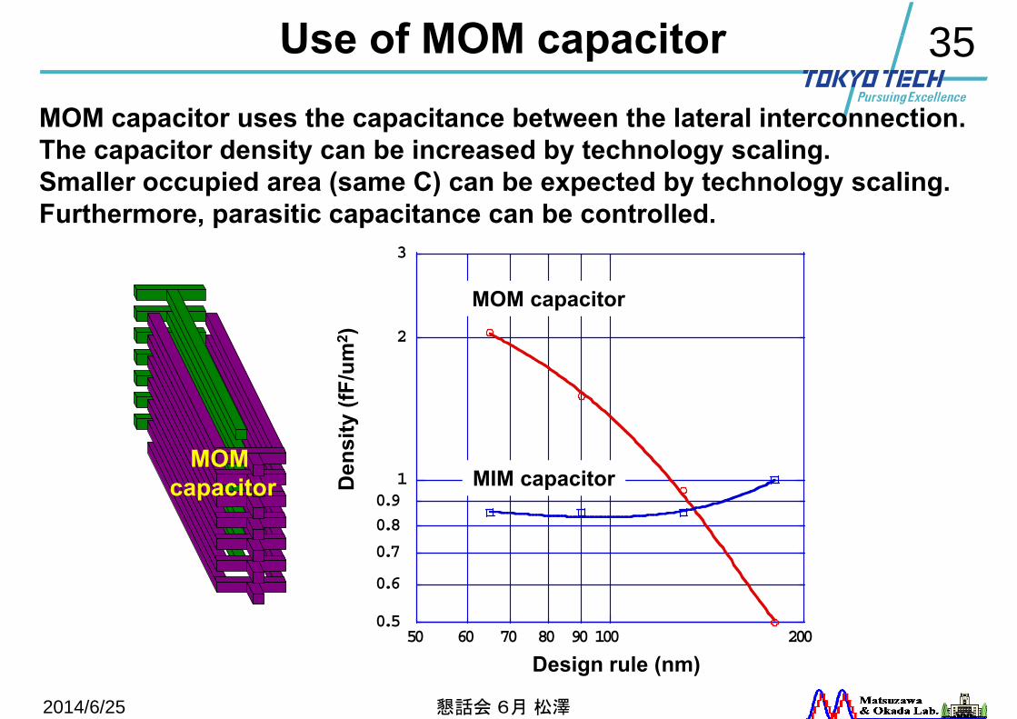
Use of MOM capacitor
MOM capacitor
2014/6/25 懇話会 6月 松澤
MOM capacitor uses the capacitance between the lateral interconnection.The capacitor density can be increased by technology scaling.Smaller occupied area (same C) can be expected by technology scaling.Furthermore, parasitic capacitance can be controlled.
36Scalable power dissipation
2014/6/25
0.0
0.5
1.0
1.5
2.0
2.5
3.0
3.5
4.0
4.5
5.0
0 10 20 30 40 50 60 70 80
Pow
er d
issi
patio
n [m
W]
Sampling frequency [MHz]
1.2V1.0V0.8V
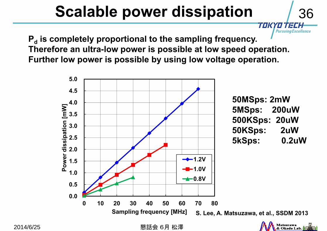
50MSps: 2mW5MSps: 200uW500KSps: 20uW50KSps: 2uW5kSps: 0.2uW
S. Lee, A. Matsuzawa, et al., SSDM 2013
懇話会 6月 松澤
Pd is completely proportional to the sampling frequency.Therefore an ultra-low power is possible at low speed operation.Further low power is possible by using low voltage operation.
37Performance comparison
2014/6/25
[3] W. Liu, P. Huang, Y. Chiu, ISSCC, pp. 380-381, Feb. 2010.[4] T. Morie, et al., ISSCC, pp.272-273, Feb. 2013.
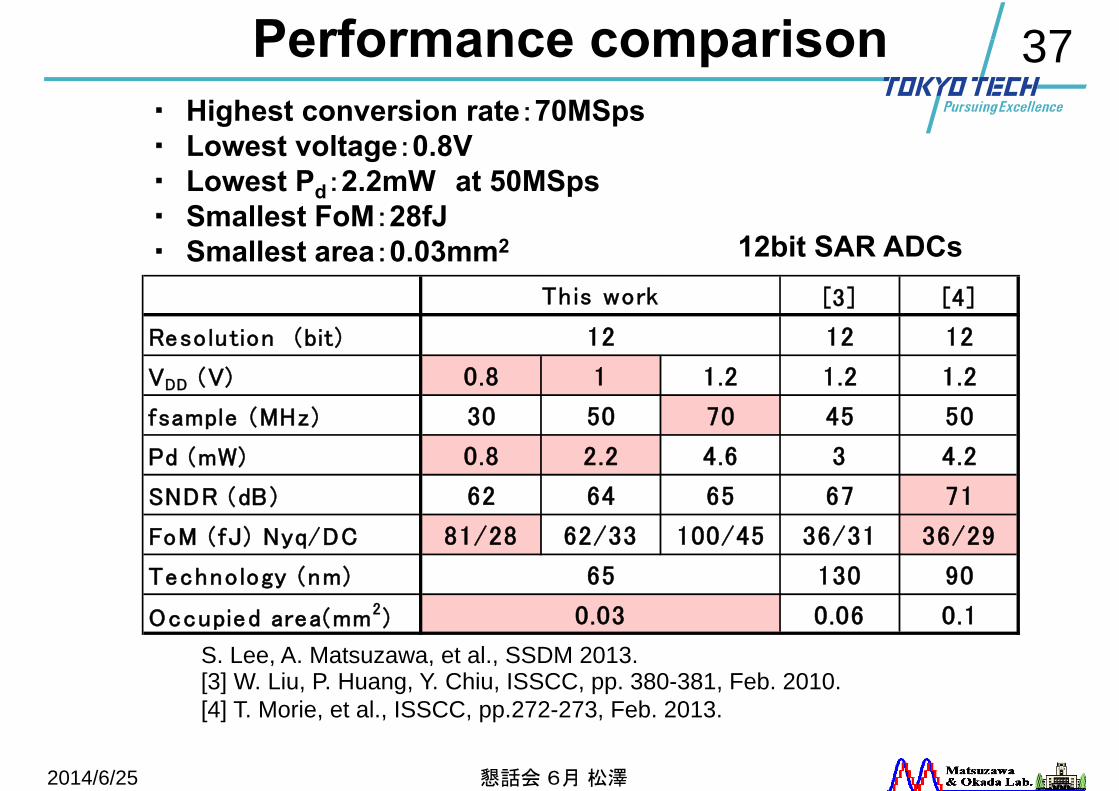
・ Highest conversion rate:70MSps・ Lowest voltage:0.8V・ Lowest Pd:2.2mW at 50MSps・ Smallest FoM:28fJ・ Smallest area:0.03mm2 12bit SAR ADCs
[3] [4]
Resolution (bit) 12 12
VDD (V) 0.8 1 1.2 1.2 1.2
fsample (MHz) 30 50 70 45 50
Pd (mW) 0.8 2.2 4.6 3 4.2
SNDR (dB) 62 64 65 67 71
FoM (fJ) Nyq/DC 81/28 62/33 100/45 36/31 36/29
Technology (nm) 130 90
Occupied area(mm2) 0.06 0.1
This work
12
65
0.03
S. Lee, A. Matsuzawa, et al., SSDM 2013.
懇話会 6月 松澤
38Performance scalable ADC ?
2014/6/25
50
60
70
80
90
0.1 1 10 100
SNR
[dB
]
BW [MHz]
SDCT SDSC VCO
135dB
143dB
150dB
ISSCC 2008-2013VLSI Symp. 2008-2012
SAR ADC w/ OVS
Interleaving
Over sampling
1V, 50MSps Operation
1
10
100
0.1 1 10 100BW [MHz]
SDCT SDSC VCOISSCC 2008-2013VLSI Symp. 2008-2012
This ADC
Over sampling Optimized
Pow
er d
issi
patio
n (m
W)
S. Lee, A. Matsuzawa, et al., SSDM 2013
懇話会 6月 松澤
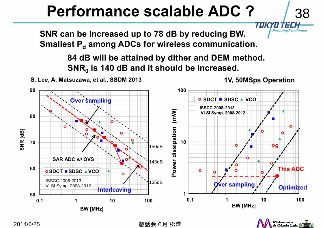
SNR can be increased up to 78 dB by reducing BW.Smallest Pd among ADCs for wireless communication.
84 dB will be attained by dither and DEM method.SNR0 is 140 dB and it should be increased.
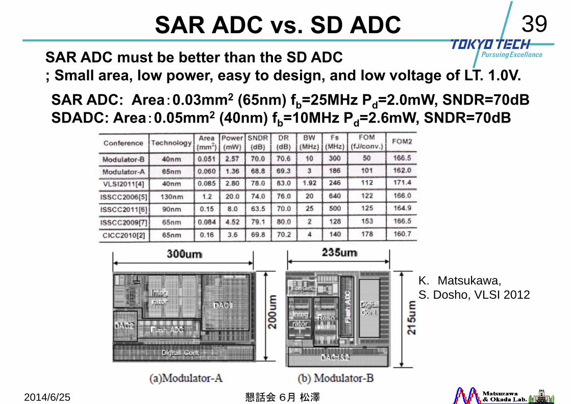
39SAR ADC vs. SD ADC
K. Matsukawa,S. Dosho, VLSI 2012
SAR ADC: Area:0.03mm2 (65nm) fb=25MHz Pd=2.0mW, SNDR=70dBSDADC: Area:0.05mm2 (40nm) fb=10MHz Pd=2.6mW, SNDR=70dB
SAR ADC must be better than the SD ADC; Small area, low power, easy to design, and low voltage of LT. 1.0V.
2014/6/25 懇話会 6月 松澤
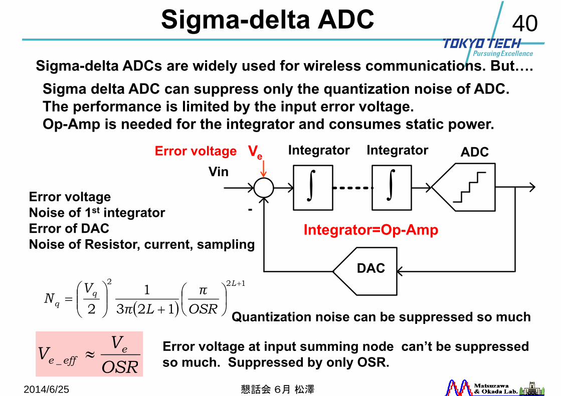
40Sigma-delta ADC
DAC
Vin
ADCIntegrator Integrator
-
VeError voltage
122
1231
2
Lq
q OSRπ
LπV
N
OSRVV e
effe _
Quantization noise can be suppressed so much
Error voltageNoise of 1st integratorError of DACNoise of Resistor, current, sampling
Error voltage at input summing node can’t be suppressedso much. Suppressed by only OSR.
Sigma delta ADC can suppress only the quantization noise of ADC.The performance is limited by the input error voltage.Op-Amp is needed for the integrator and consumes static power.
Sigma-delta ADCs are widely used for wireless communications. But….
Integrator=Op-Amp
2014/6/25 懇話会 6月 松澤
41
7bit 2.2GSps ADC
using time-domain signal processing
2014/6/25 懇話会 6月 松澤
427bit 2.2GSps ADC for 60GHz ABB
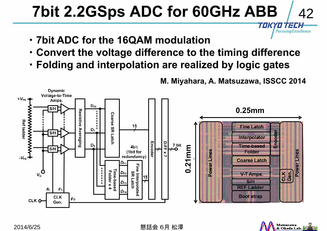
2014/6/25
Encoder
Coarse SR
LatchTim
e-basedFolder x 4
Fine InterpolatedSR
Latch
D-FF x 7
Resistive A
veraging
Ref ladder
・7bit ADC for the 16QAM modulation・Convert the voltage difference to the timing difference・Folding and interpolation are realized by logic gates
M. Miyahara, A. Matsuzawa, ISSCC 2014
0.25mm
0.21
mm
懇話会 6月 松澤
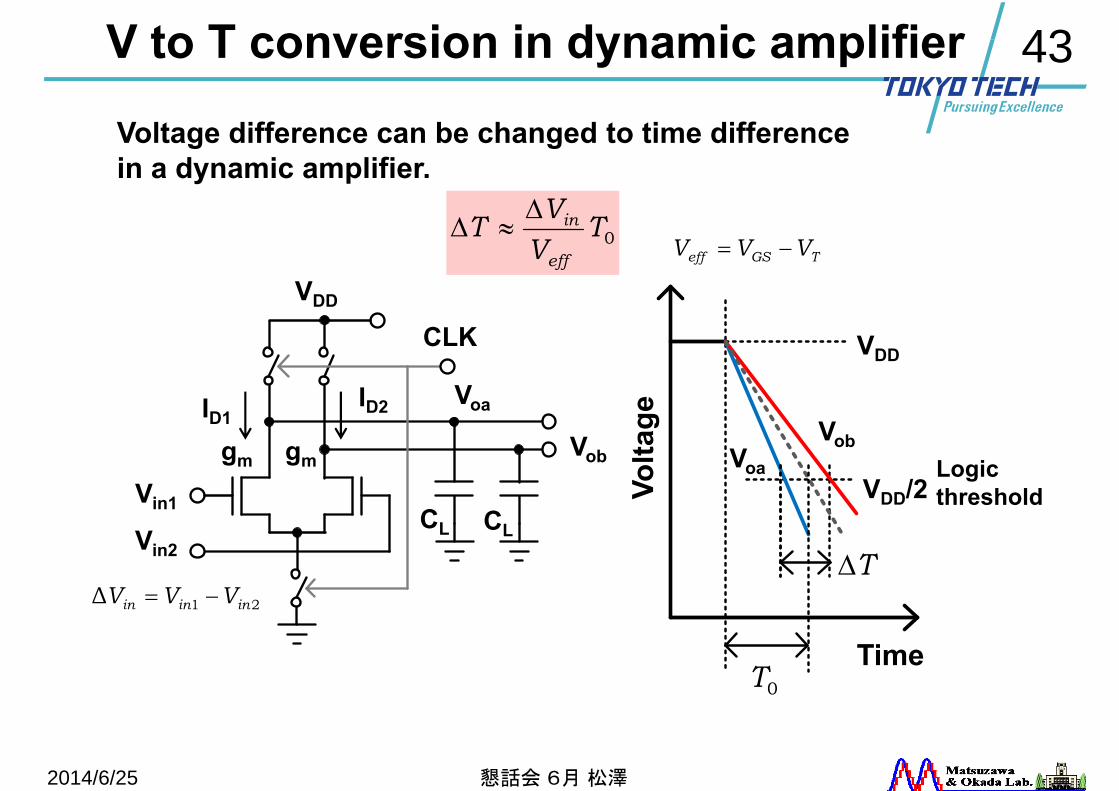
43V to T conversion in dynamic amplifier
Vin1
Vin2
VDD
CLK
CL CL
21Δ ininin VVV
TimeVo
ltage
Voa
Vobgm gm Voa
Vob
T
ID1ID2
VDD
VDD/2Logic threshold
0T
0TVVTeff
in
TGSeff VVV
Voltage difference can be changed to time difference in a dynamic amplifier.
2014/6/25 懇話会 6月 松澤
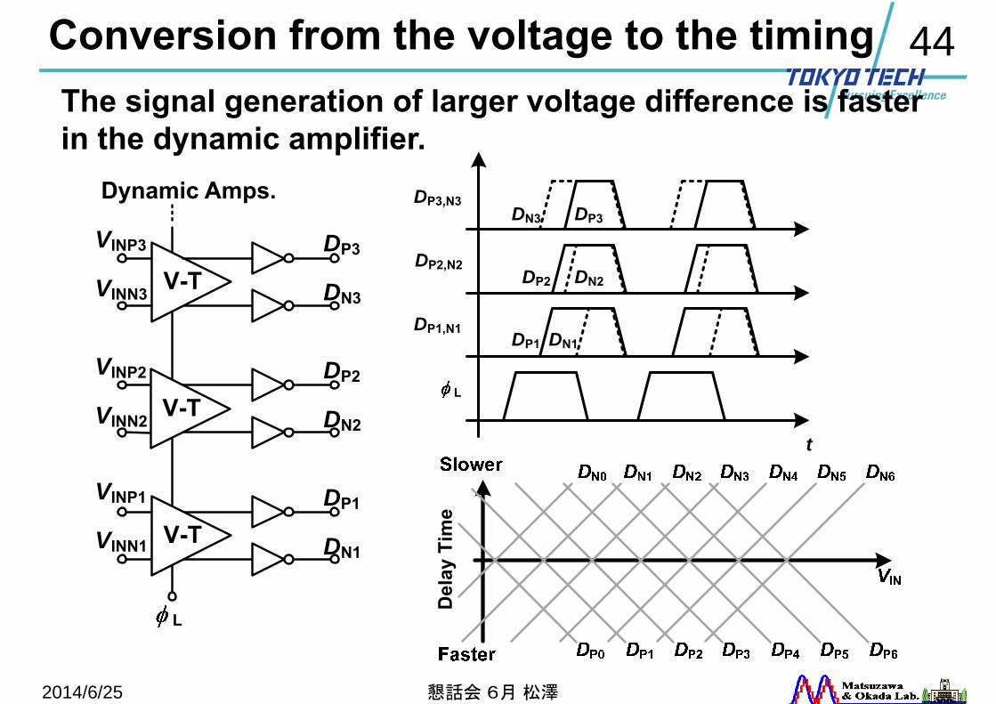
44Conversion from the voltage to the timing
DP3
DN3
DP2
DN2
DP1
DN1
L
VINP3
VINN3
VINP2
VINN2
VINP1
VINN1
L
DP1,N1
DP2,N2
DP3,N3
t
DP1 DN1
DP2 DN2
DN3 DP3
Del
ay T
ime
2014/6/25 懇話会 6月 松澤
The signal generation of larger voltage difference is fasterin the dynamic amplifier.
Dynamic Amps.
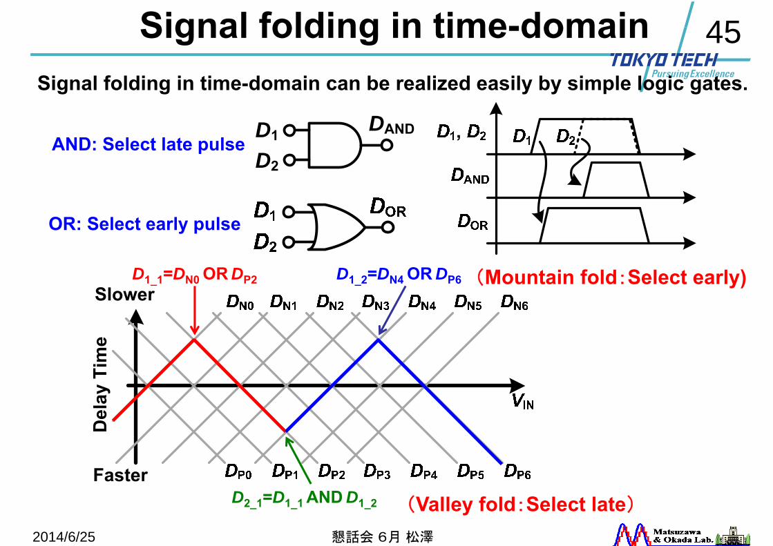
45Signal folding in time-domain
D2_1=D1_1 AND D1_2
D1_1=DN0 OR DP2 D1_2=DN4 OR DP6
D1
D2
DAND
(Valley fold:Select late)
(Mountain fold:Select early)
2014/6/25
OR: Select early pulse
AND: Select late pulse
懇話会 6月 松澤
Signal folding in time-domain can be realized easily by simple logic gates.
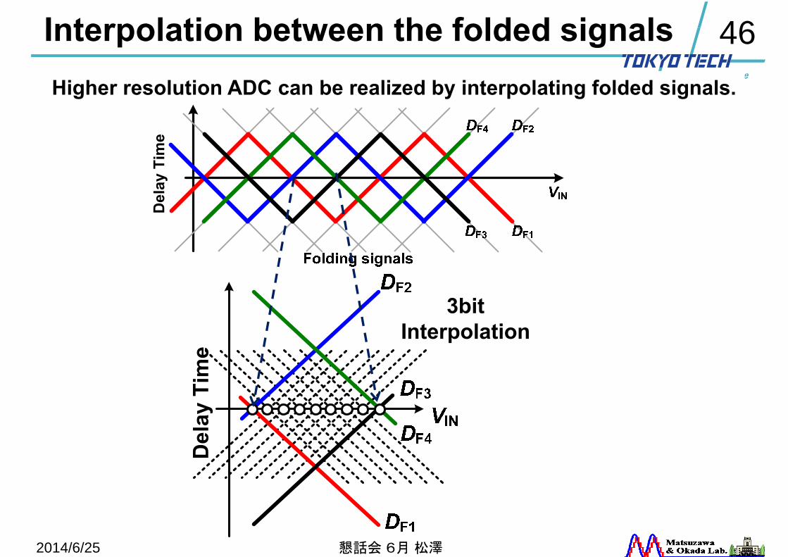
46Interpolation between the folded signals
Del
ay T
ime
2014/6/25 懇話会 6月 松澤
Higher resolution ADC can be realized by interpolating folded signals.
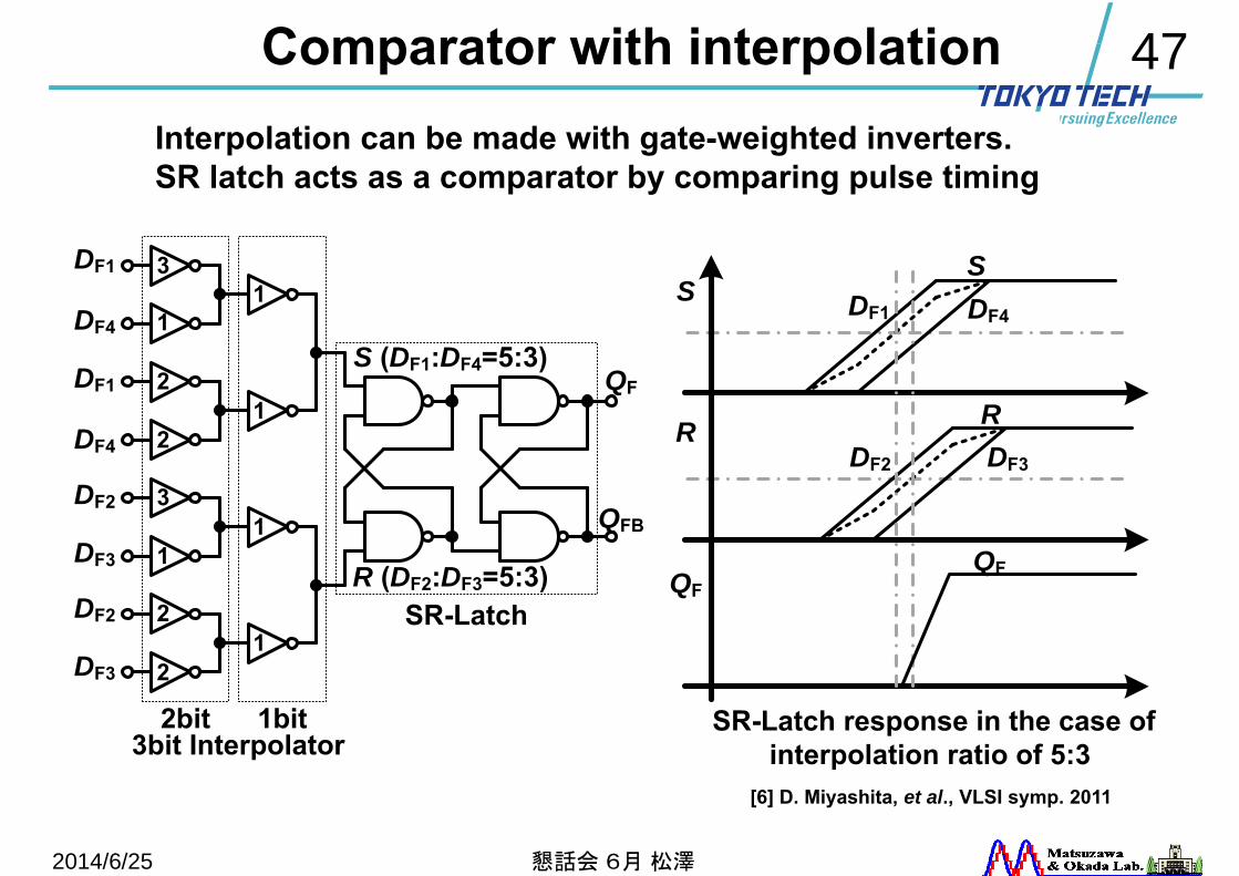
47Comparator with interpolation
QF
QFB
DF1
DF4
DF2
DF3
DF1
DF4
DF2
DF3
S DF1 DF4
R DF2 DF3
3
1
2
2
3
1
2
2
1
1
1
1
DF1 DF4
S
DF2
R
QF
S
R
QF
DF3
[6] D. Miyashita, et al., VLSI symp. 2011
2014/6/25 懇話会 6月 松澤
Interpolation can be made with gate-weighted inverters.SR latch acts as a comparator by comparing pulse timing
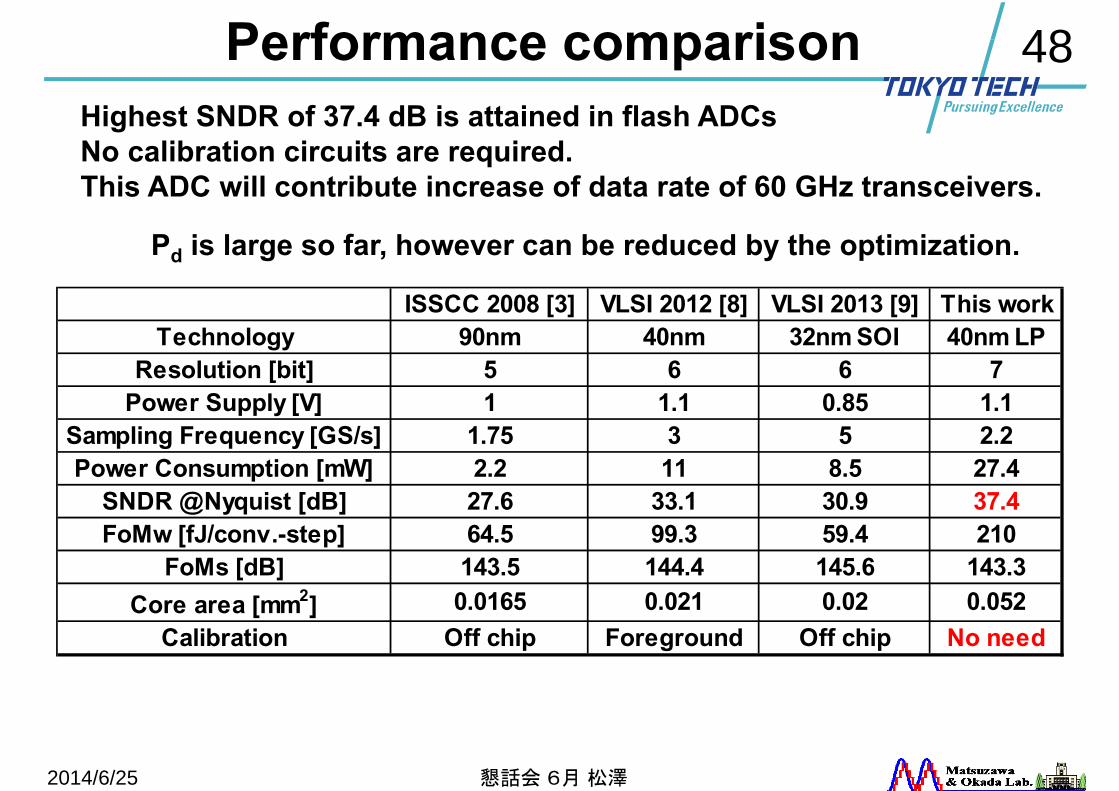
48Performance comparison
2014/6/25
ISSCC 2008 [3] VLSI 2012 [8] VLSI 2013 [9] This workTechnology 90nm 40nm 32nm SOI 40nm LP
Resolution [bit] 5 6 6 7Power Supply [V] 1 1.1 0.85 1.1
Sampling Frequency [GS/s] 1.75 3 5 2.2Power Consumption [mW] 2.2 11 8.5 27.4
SNDR @Nyquist [dB] 27.6 33.1 30.9 37.4FoMw [fJ/conv.-step] 64.5 99.3 59.4 210
FoMs [dB] 143.5 144.4 145.6 143.3Core area [mm2] 0.0165 0.021 0.02 0.052
Calibration Off chip Foreground Off chip No need
懇話会 6月 松澤
Highest SNDR of 37.4 dB is attained in flash ADCsNo calibration circuits are required. This ADC will contribute increase of data rate of 60 GHz transceivers.
Pd is large so far, however can be reduced by the optimization.
49
PLL
2014/6/25 懇話会 6月 松澤
PLL that can generate accurate frequency and timingwill be improved continuously.
50Progress of PLL
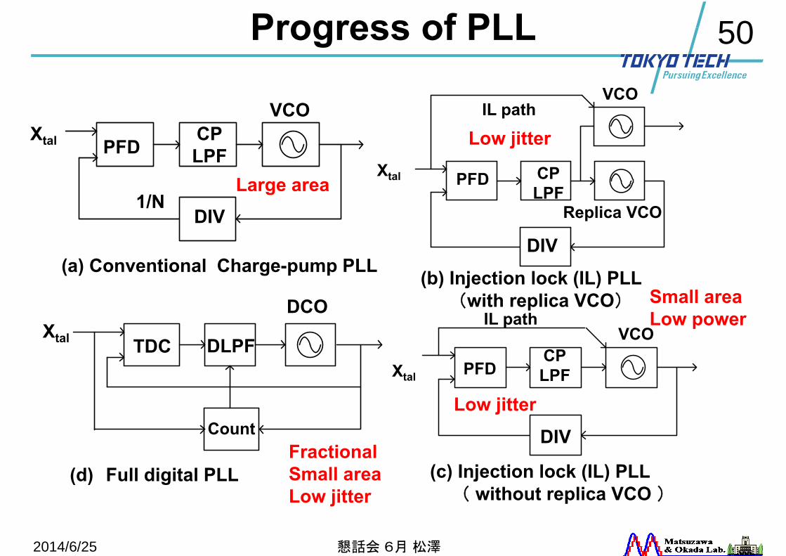
2014/6/25
Xtal PFDCPLPF
VCO
1/NDIV
(a) Conventional Charge-pump PLL
Xtal
(b) Injection lock (IL) PLL(with replica VCO)
PFD CPLPF
Replica VCO
VCOIL path
Xtal TDC
Count
DCO
DLPFXtal
(c) Injection lock (IL) PLL( without replica VCO )
DIV
DIV
PFDCPLPF
VCOIL path
(d) Full digital PLL
Small areaLow power
Low jitter
Fractional Small areaLow jitter
Large area
懇話会 6月 松澤
Low jitter
51
2014/6/25
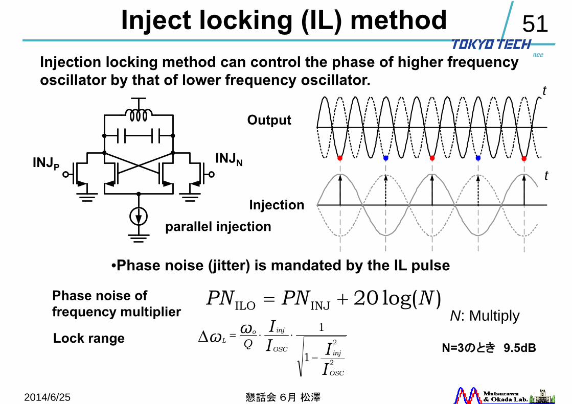
Inject locking (IL) method
Output
INJPINJN
Injection
N: Multiply
t
t
Phase noise of frequency multiplier
parallel injection
)log(20INJILO NPNPN
N=3のとき 9.5dB
III
Iωω
OSC
injOSC
injoL Q
2
2
1
1
Lock range
懇話会 6月 松澤
Injection locking method can control the phase of higher frequency oscillator by that of lower frequency oscillator.
•Phase noise (jitter) is mandated by the IL pulse
52
2014/6/25
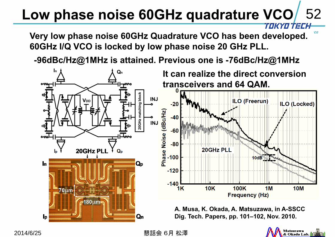
Low phase noise 60GHz quadrature VCO
VDD
INJp
INJn
Ip
In
Qp
Qn
20G
Hzm
atch
ing
bloc
k
-96dBc/Hz@1MHz is attained. Previous one is -76dBc/Hz@1MHz
A. Musa, K. Okada, A. Matsuzawa, in A-SSCC Dig. Tech. Papers, pp. 101–102, Nov. 2010.
懇話会 6月 松澤
Very low phase noise 60GHz Quadrature VCO has been developed.60GHz I/Q VCO is locked by low phase noise 20 GHz PLL.
It can realize the direct conversion transceivers and 64 QAM.
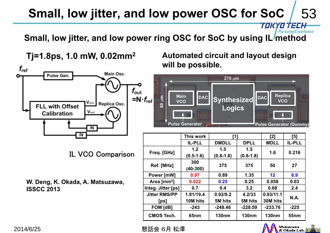
53Small, low jitter, and low power OSC for SoC
2014/6/25
This work [1] [2] [5]IL-PLL DMDLL DPLL MDLL IL-PLL
Freq. [GHz] 1.2(0.5-1.6)
1.5(0.8-1.8)
1.5(0.8-1.8) 1.6 0.216
Ref. [MHz] 300(40-300) 375 375 50 27
Power [mW] 0.97 0.89 1.35 12 6.9Area [mm2] 0.022 0.25 0.25 0.058 0.03
Integ. Jitter [ps] 0.7 0.4 3.2 0.68 2.4Jitter RMS/PP
[ps]1.81/19.410M hits
0.92/9.25M hits
4.2/335M hits
0.93/11.130M hits N.A.
FOM [dB] -243 -248.46 -228.59 -233.76 -225
CMOS Tech. 65nm 130nm 130nm 130nm 55nm
IL VCO Comparison
Tj=1.8ps, 1.0 mW, 0.02mm2 Automated circuit and layout design will be possible.
W. Deng, K. Okada, A. Matsuzawa,ISSCC 2013
懇話会 6月 松澤
Small, low jitter, and low power ring OSC for SoC by using IL method
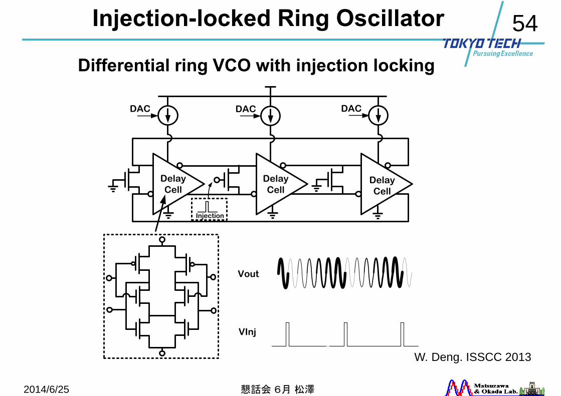
54Injection-locked Ring Oscillator
Injection
Delay Cell
Delay Cell
Delay Cell
DAC DAC DAC
Vout
VInj
Differential ring VCO with injection locking
W. Deng. ISSCC 2013
2014/6/25 懇話会 6月 松澤
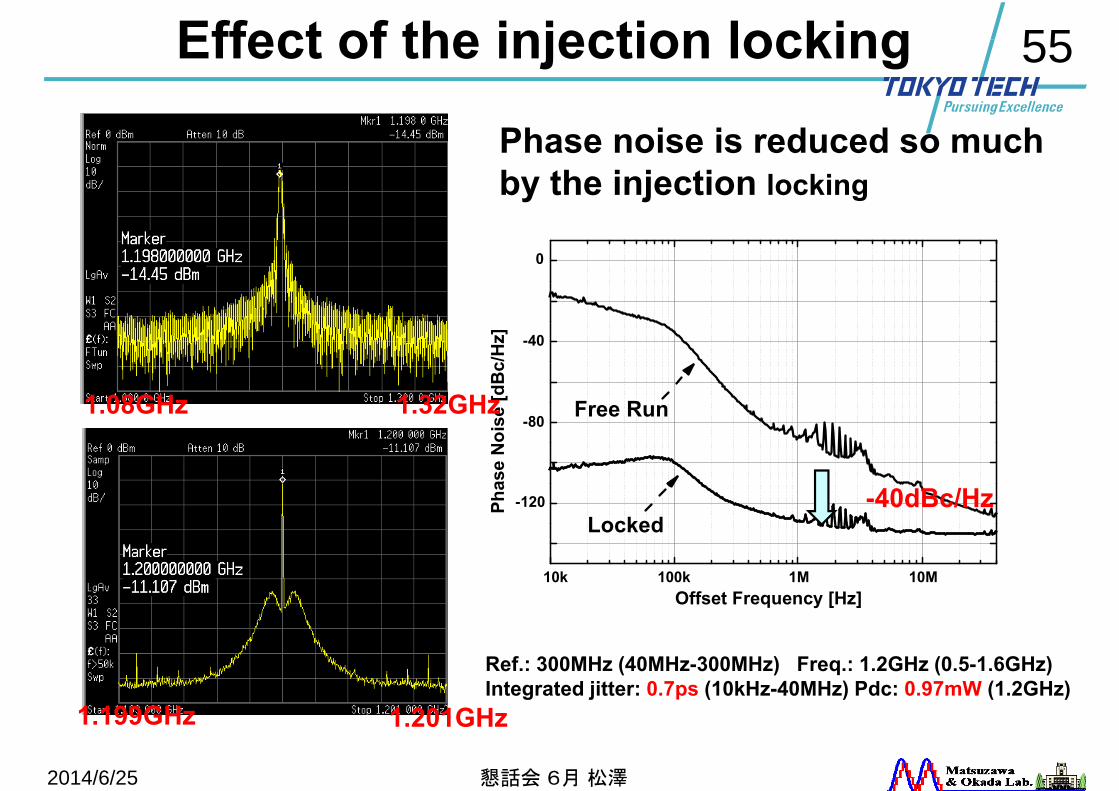
55Effect of the injection locking
Free Run
Locked
Offset Frequency [Hz]
Phas
e N
oise
[dB
c/H
z]
10k 100k 1M 10M
-120
-80
-40
0
Ref.: 300MHz (40MHz-300MHz) Freq.: 1.2GHz (0.5-1.6GHz)Integrated jitter: 0.7ps (10kHz-40MHz) Pdc: 0.97mW (1.2GHz)
1.08GHz 1.32GHz
1.199GHz 1.201GHz
-40dBc/Hz
Phase noise is reduced so muchby the injection locking
2014/6/25 懇話会 6月 松澤
56High precision Time to Digital Converter
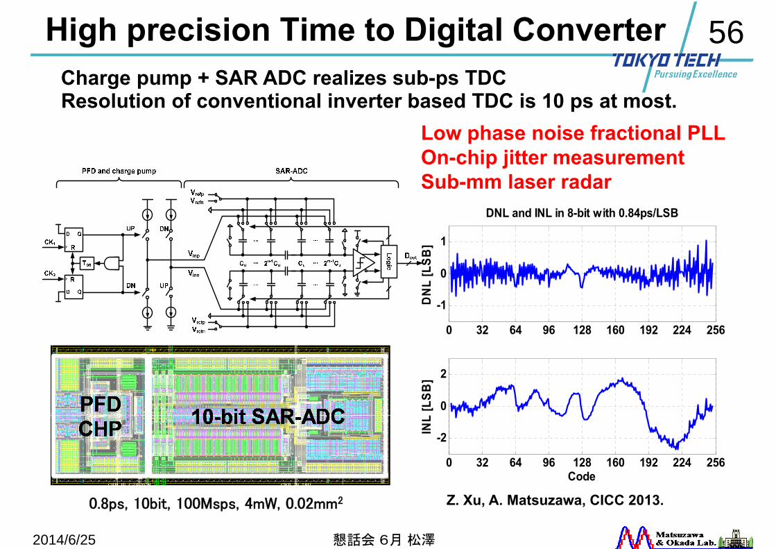
2014/6/25
0 32 64 96 128 160 192 224 256
-1
0
1
DNL and INL in 8-bit with 0.84ps/LSB
DN
L [L
SB]
0 32 64 96 128 160 192 224 256
-2
0
2
Code
INL
[LSB
]
Resolution of conventional inverter based TDC is 10 ps at most.
0.8ps, 10bit, 100Msps, 4mW, 0.02mm2 Z. Xu, A. Matsuzawa, CICC 2013.
懇話会 6月 松澤
Charge pump + SAR ADC realizes sub-ps TDC
Low phase noise fractional PLLOn-chip jitter measurementSub-mm laser radar
57Expectation of full digital PLL
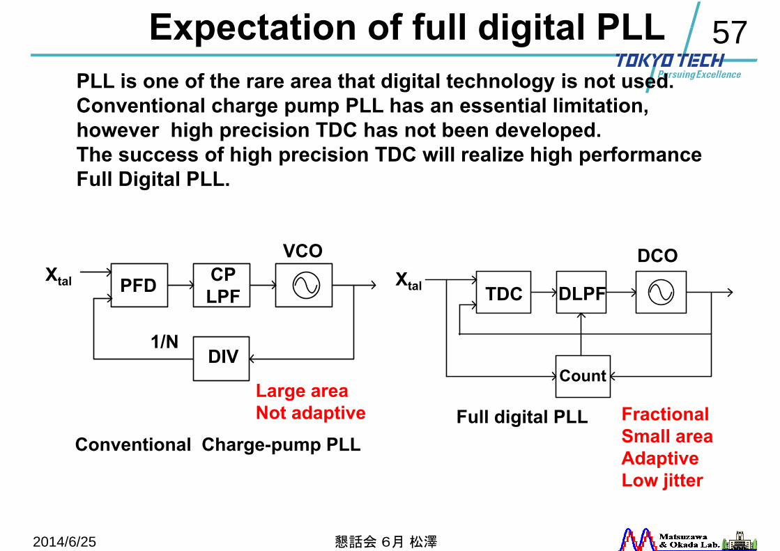
2014/6/25
Xtal TDC
Count
DCO
DLPFXtal PFD CP
LPF
VCO
1/NDIV
懇話会 6月 松澤
Conventional Charge-pump PLLFull digital PLL Fractional
Small areaAdaptiveLow jitter
Large areaNot adaptive
PLL is one of the rare area that digital technology is not used.Conventional charge pump PLL has an essential limitation,however high precision TDC has not been developed.The success of high precision TDC will realize high performanceFull Digital PLL.
58
2014/6/25 懇話会 6月 松澤
Layout-driven circuit design and programmable analog circuit technique
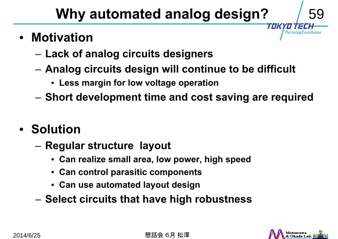
59Why automated analog design?• Motivation
– Lack of analog circuits designers– Analog circuits design will continue to be difficult
• Less margin for low voltage operation– Short development time and cost saving are required
• Solution– Regular structure layout
• Can realize small area, low power, high speed• Can control parasitic components• Can use automated layout design
– Select circuits that have high robustness
2014/6/25 懇話会 6月 松澤
60
MSB
Top
Plat
e
Parasitic cap. (3.5fF)
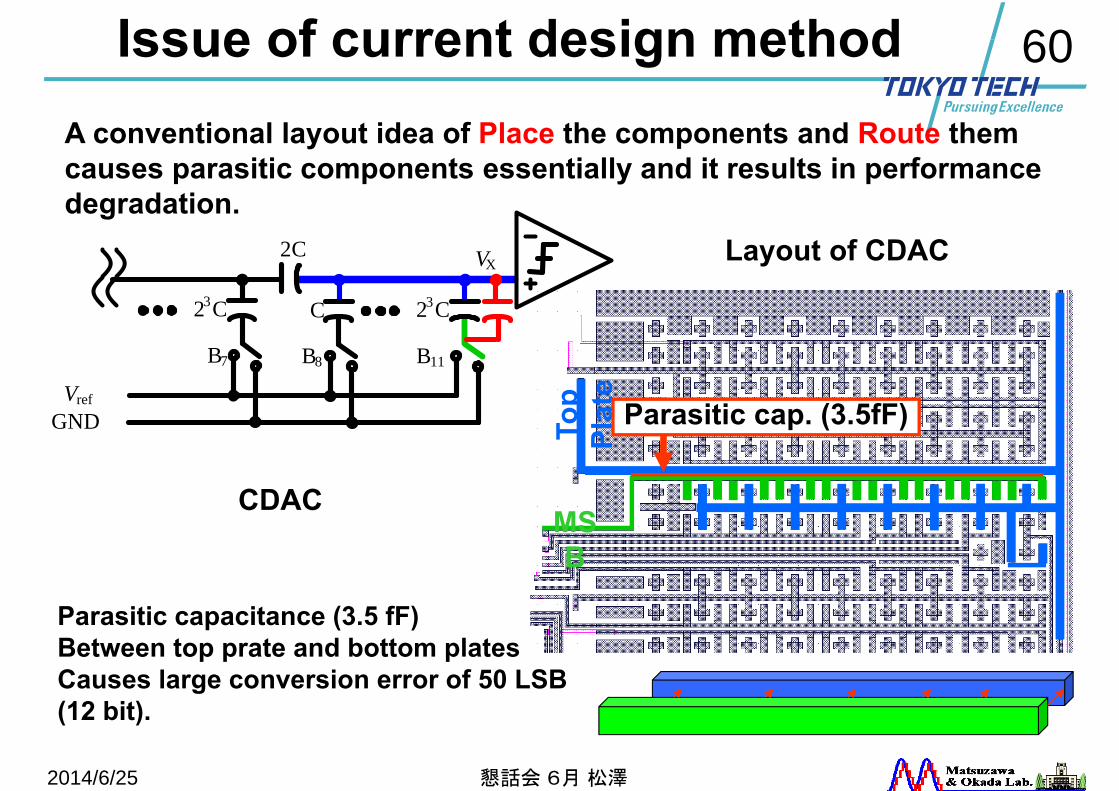
Issue of current design method
23C
Vref
GND
VX
B7
23CC
B8 B11
2C Layout of CDAC
CDAC
2014/6/25 懇話会 6月 松澤
Parasitic capacitance (3.5 fF)Between top prate and bottom platesCauses large conversion error of 50 LSB(12 bit).
A conventional layout idea of Place the components and Route themcauses parasitic components essentially and it results in performancedegradation.
61
2014/6/25
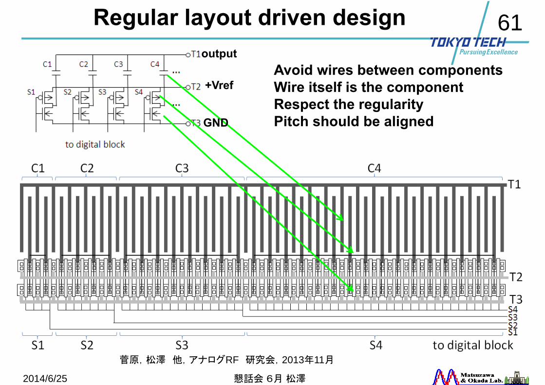
Regular layout driven designoutput
+Vref
GND
菅原,松澤 他,アナログRF 研究会,2013年11月
懇話会 6月 松澤
Avoid wires between componentsWire itself is the componentRespect the regularity Pitch should be aligned
62Ideal layout design
2014/6/25
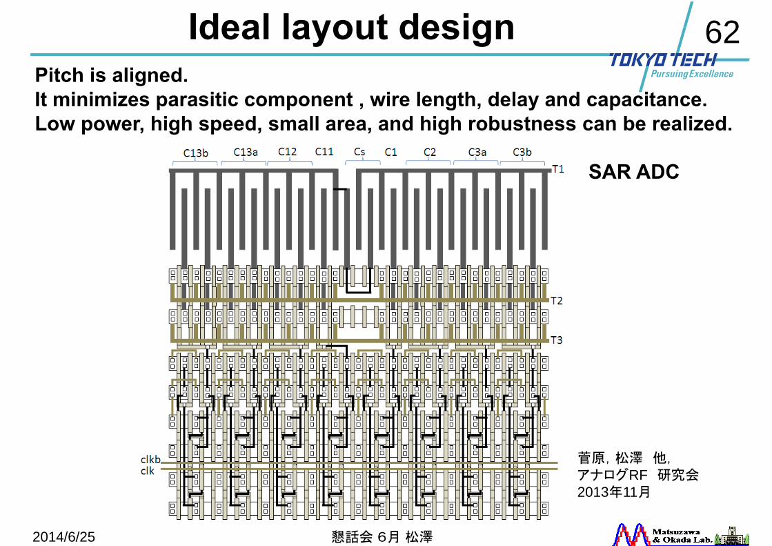
SAR ADC
菅原,松澤 他,アナログRF 研究会2013年11月
懇話会 6月 松澤
Pitch is aligned.It minimizes parasitic component , wire length, delay and capacitance.Low power, high speed, small area, and high robustness can be realized.
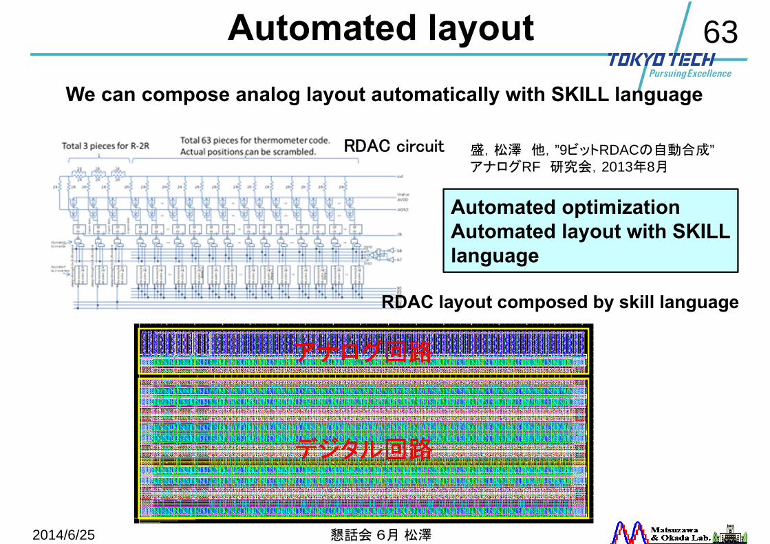
63Automated layout
2014/6/25
RDAC circuit
RDAC layout composed by skill language
Automated optimizationAutomated layout with SKILL language
盛,松澤 他,”9ビットRDACの自動合成”アナログRF 研究会,2013年8月
懇話会 6月 松澤
We can compose analog layout automatically with SKILL language
64
2014/6/25
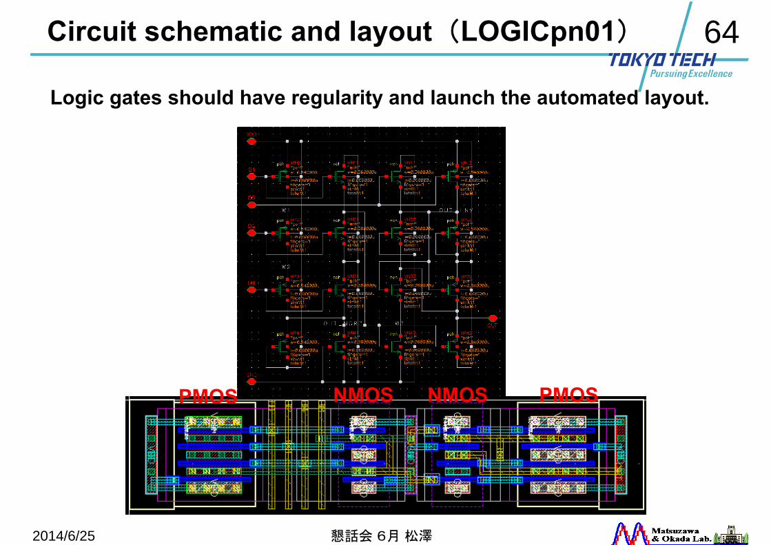
Circuit schematic and layout(LOGICpn01)
PMOS PMOSNMOSNMOS
懇話会 6月 松澤
Logic gates should have regularity and launch the automated layout.
65
2014/6/25
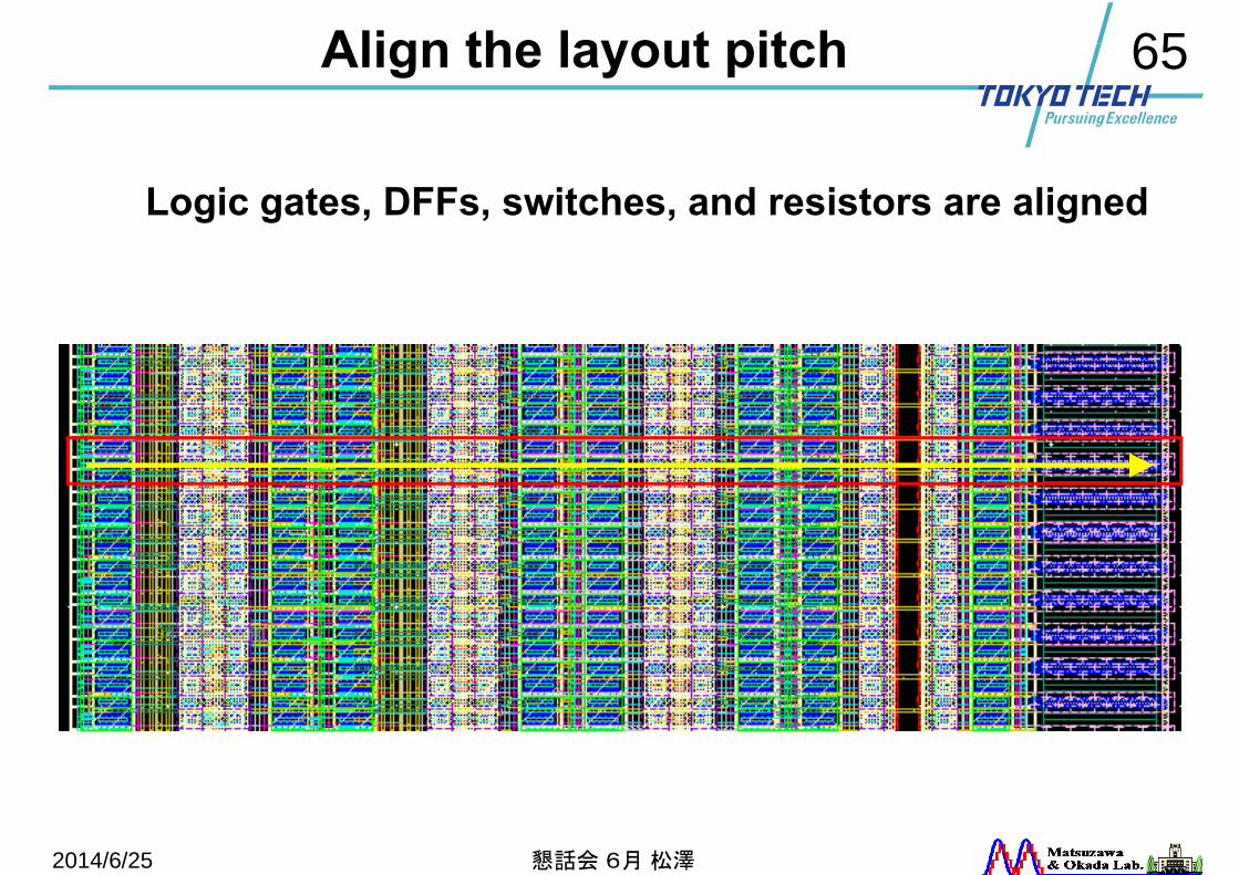
Align the layout pitch
懇話会 6月 松澤
Logic gates, DFFs, switches, and resistors are aligned
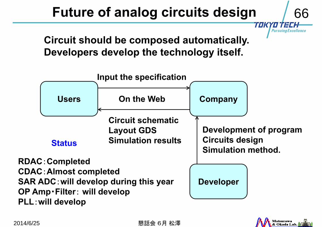
66Future of analog circuits design
2014/6/25
Users Company
Developer
Input the specification
Circuit schematicLayout GDSSimulation results
On the Web
RDAC:CompletedCDAC:Almost completedSAR ADC:will develop during this yearOP Amp・Filter: will develop PLL:will develop
Status
懇話会 6月 松澤
Development of programCircuits designSimulation method.
Circuit should be composed automatically.Developers develop the technology itself.
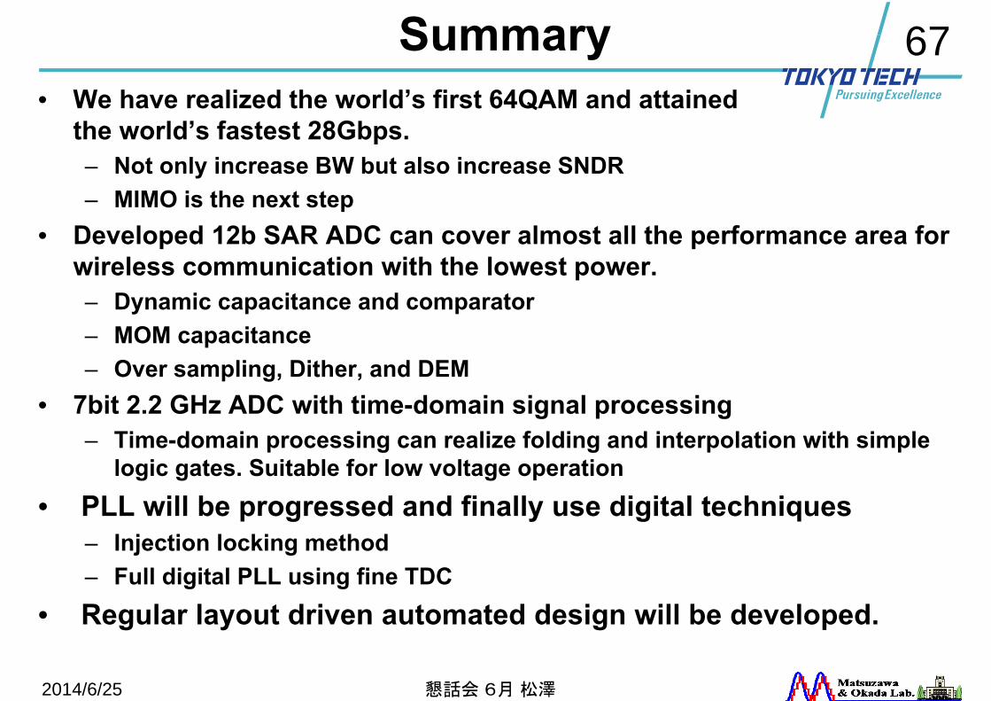
67Summary• We have realized the world’s first 64QAM and attained
the world’s fastest 28Gbps.– Not only increase BW but also increase SNDR– MIMO is the next step
• Developed 12b SAR ADC can cover almost all the performance area for wireless communication with the lowest power.– Dynamic capacitance and comparator– MOM capacitance– Over sampling, Dither, and DEM
• 7bit 2.2 GHz ADC with time-domain signal processing– Time-domain processing can realize folding and interpolation with simple
logic gates. Suitable for low voltage operation• PLL will be progressed and finally use digital techniques
– Injection locking method– Full digital PLL using fine TDC
• Regular layout driven automated design will be developed.
2014/6/25 懇話会 6月 松澤