Embed Size (px)
Citation preview

Sources: TSR, Katz, Boriello, Vahid, Perkowski
CSE140: Components and Design Techniques
for Digital Systems
Register Transfer Level (RTL) Design based on Vahid chap. 5
Tajana Simunic Rosing

Sources: TSR, Katz, Boriello, Vahid, Perkowski
RTL Design Method

Sources: TSR, Katz, Boriello, Vahid, Perkowski
RTL Design example: Laser-Based Distance Measurer
• Laser-based distance measurement – pulse laser,
measure time T to sense reflection
– Laser light travels at speed of light, 3*108 m/sec
– Distance is thus D = T sec * 3*108 m/sec / 2
Object of
interest
D
2D = T sec * 3*108 m/sec
sensor
laser
T (in seconds)

Sources: TSR, Katz, Boriello, Vahid, Perkowski
Step 4: Deriving the Controller’s FSM
• FSM has same structure as high-level state machine
– Inputs/outputs all bits now
– Replace data operations by bit operations using datapath
300 M H z Clock
D
B L
S
16
t o displ a y
f r om but t on C o n t r oller
t o laser
f r om sensor
D a tap a th
D r eg_clr
D r eg_ld
D c tr_clr
D c tr_c n t
Inputs: B, S
Outputs: L, Dreg_clr, Dreg_ld, Dctr_clr, Dctr_cnt
S0 S1 S2 S3
L = 0 L = 1 L = 0 L = 0
B’ S’
B S S4
L = 0
Inputs: B, S (1 bit each) Outputs: L (bit), D (16 bits) Local Registers: Dctr (16 bits)
S0 S1 S2 S3
L = 0 D = 0
L = 1 L=0 Dctr = Dctr + 1
Dctr = 0
B’ S’
B S
D = Dctr / 2 (calculate D)
S4
Dreg_clr = 1
Dreg_ld = 0
Dctr_clr = 0
Dctr_cnt = 0
(laser off)
(clear D reg)
Dreg_clr = 0
Dreg_ld = 0
Dctr_clr = 1
Dctr_cnt = 0
(clear count)
Dreg_clr = 0
Dreg_ld = 0
Dctr_clr = 0
Dctr_cnt = 0
(laser on)
Dreg_clr = 0
Dreg_ld = 0
Dctr_clr = 0
Dctr_cnt = 1
(laser off)
(count up)
Dreg_clr = 0
Dreg_ld = 1
Dctr_clr = 0
Dctr_cnt = 0
(load D reg with Dctr/2)
(stop counting)

Sources: TSR, Katz, Boriello, Vahid, Perkowski
RTL Design Method Example
• Soda dispenser
– c: bit input, 1 when coin
deposited
– a: 8-bit input having value of
deposited coin
– s: 8-bit input having cost of a
soda
– d: bit output, processor sets
to 1 when total value of
deposited coins equals or
exceeds cost of a soda
a s
c
d Soda
dispenser processor
25
1 0 25
1
1
50 0
0
0
0
tot:
25
tot:
50

Sources: TSR, Katz, Boriello, Vahid, Perkowski
Step 1: Capture High-Level State Machine
• Declare local register tot
• Init state: Set d=0, tot=0
• Wait state: wait for coin – If see coin, go to Add state
• Add state: Update total value: tot = tot + a
– Remember, a is present coin’s value
– Go back to Wait state
• In Wait state, if tot >= s, go to Disp(ense) state
• Disp state: Set d=1 (dispense soda)
– Return to Init state
Inputs: c (bit), a (8 bits), s (8 bits)
Outputs: d (bit)
Local registers: tot (8 bits)
Wait
Add
Disp
I nit
d=0
tot=0
c’*(tot<s)
d=1
c
tot=tot+a
8 8 a s
c d
Soda dispenser processor
c’*(tot<s)’ Not an FSM because:
•Multi-bit (data) inputs a and s
•Local register tot
•Data operations tot=0, tot<s, tot=tot+a.
Useful high-level state machine:
•Data types beyond just bits
•Local registers
•Arithmetic equations/expressions
Sources: TSR, Katz, Boriello, Vahid, Perkowski
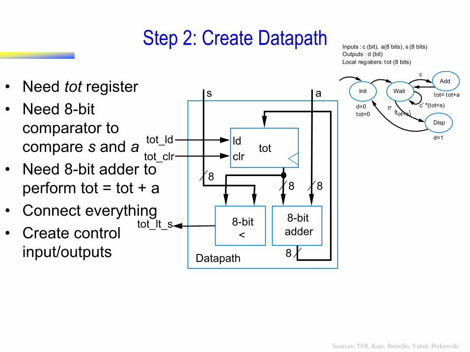
Step 2: Create Datapath
• Need tot register
• Need 8-bit
comparator to
compare s and a
• Need 8-bit adder to
perform tot = tot + a
• Connect everything
• Create control
input/outputs
ld
clr tot
8-bit
<
8-bit
adder
8
8
8 8
s a
Datapath
tot_ld
tot_clr
tot_lt_s
I nputs : c (bit), a(8 bits) , s (8 bits)
O utputs : d (bit)
L ocal r e g is t ers : t ot (8 bits)
W ait
A dd
Disp
I nit
d=0
t ot=0
c ‘ ( t ot<s) ‘
c ‘ * ( t ot<s)
d=1
c
t ot= t ot+a

Sources: TSR, Katz, Boriello, Vahid, Perkowski
Step 3: Connect Datapath to a Controller
• Controller’s inputs
– External input c
(coin detected)
– Input from datapath
comparator’s
output, which we
named tot_lt_s
• Controller’s outputs
– External output d
(dispense soda)
– Outputs to datapath
to load and clear
the tot register
tot_lt_s
tot_clr
tot_ld
Controller Datapath
s
c
d
a
8 8
ld
clr t ot
8-bit
<
8-bit
adder
8
8
8 8
s a
D a tap a th
t ot_ld
t ot_clr
t ot_lt_s

Sources: TSR, Katz, Boriello, Vahid, Perkowski
Step 4 – Derive the Controller’s FSM
• Same states
and arcs as
high-level
state
machine
• But set/read
datapath
control
signals for all
datapath
operations
and
conditions
tot_lt_s
tot_clr
tot_ld
Contr
olle
r
Data
path
s
c
d
a
8 8
ld
clr tpt
8-bit <
8-bit adder
8
8
8 8
s a
Datapath
tot_ld
tot_clr
tot_lt_s
Inputs: : c , tot_lt_s (bit)
Outputs: d , tot_ld , tot_clr (bit)
W ait
Disp
I nit
d=0 tot_clr=1
c ’ * tot_lt_s
d=1
c
tot_ld=1
c
d
tot_ld
tot_clr
tot_lt_s
Controller
Add

Sources: TSR, Katz, Boriello, Vahid, Perkowski
Completing the Design
• Implement the FSM as a
state register and logic
d
0
0
0
0
0
0
0
0
0
1
0
0
0
0
0
0
0
0
1
0
1
1
1
1
0
0
0
0
0
0
n0
1
1
1
1
1
1
0
0
1
0
n1
0
0
0
0
1
0
1
1
0
0
0
1
0
1
0
1
0
1
0
0
c
0
0
1
1
0
0
1
1
0
0
s1
0
0
0
0
0
0
0
0
1
1
s0
0
0
0
0
1
1
1
1
0
1
tot_
lt_s
tot_
ld
tot_
clr
Init
Wait
Ad
dD
isp
Inputs: : c , tot_lt_s (bit)
Outputs: d , tot_ld , tot_clr (bit)
W ait
Disp
I nit
d=0 tot_clr=1
c ’ * tot_lt_s
d=1
c
tot_ld=1
c
d
tot_ld
tot_clr
tot_lt_s
Controller
Add

Sources: TSR, Katz, Boriello, Vahid, Perkowski
RTL Design Example: Bus Interface
• Example: Bus interface
– Master processor can read
register from any peripheral
• Each register has unique 4-bit
address
• Assume 1 register/periph.
– Sets rd=1, A=address
– Appropriate peripheral places
register data on 32-bit D lines
• Periph’s address provided on
Faddr inputs (maybe from DIP
switches, or another register)
32
4 A
r d
D
Per0 Per1 Per15
Master processor
Faddr
4
A D r d
Bus interface
Main part
Peripheral
Q 32
to/from processor bus
32 4

Sources: TSR, Katz, Boriello, Vahid, Perkowski
Step 1: Create FSM
• Step 1: Create high-level state machine
– State WaitMyAddress • Output “nothing” (“Z”) on
D, store peripheral’s register value Q into local register Q1
• Wait until this peripheral’s address is seen (A=Faddr) and rd=1
– State SendData • Output Q1 onto D, wait for
rd=0 (meaning main processor is done reading the D lines)
Inputs: rd (bit); Q (32 bits); A, Faddr (4 bits) Outputs: D (32 bits) Local register: Q1 (32 bits)
WaitMyAddress
rd’ rd
SendData
D = “Z” Q1 = Q
(A = Faddr) and rd
((A = Faddr) and rd’)
D = Q1

Sources: TSR, Katz, Boriello, Vahid, Perkowski
Step 2: Create a datapath
WaitMyAddress
Inputs: rd (bit); Q (32 bits); A, Faddr (4 bits) Outputs: D (32 bits) Local register: Q1 (32 bits)
rd’ rd
SendData
D = “Z” Q1 = Q
(A = Faddr) and rd
((A = Faddr) and rd)’
D = Q1
• Step 2: Create a datapath (a) Datapath inputs/outputs
(b) Instantiate declared registers
(c) Instantiate datapath components and connections
Datapath
Bus interface
Q1_ld ld
Q1
F Q addr
4 4 32
A
D_en
A_eq_ F addr
= (4-bit) 32
32
D

Sources: TSR, Katz, Boriello, Vahid, Perkowski
Step 3: Connect datapath to controller
Step 4: Derive controller’s FSM
WaitMyAddress
Inputs: rd (bit); Q (32 bits); A, Faddr (4 bits) Outputs: D (32 bits) Local register: Q1 (32 bits)
rd’ rd
SendData
D = “Z” Q1 = Q
(A = Faddr) and rd
((A = Faddr) and rd)’
D = Q1
rd
Inputs: rd, A_eq_Faddr (bit)
Outputs: Q1_ld, D_en (bit)
W ait M y A dd r ess
r d ‘ r d
S endD a ta
D_en = 0
Q1_ld = 1
D_en = 1
Q1_ld = 0
A_eq_ F addr
and r d
( A_eq_ F addr
and r d) ‘
Datapath Bus interface
Q1_ld ld
Q1
Faddr Q
4 4 32
A
D_en
A_eq_Faddr
= (4-bit) 32
32
D

Sources: TSR, Katz, Boriello, Vahid, Perkowski
RTL Example: Video Compression
• Video is a series of frames (e.g., 30 per second)
• Most frames similar to previous frame
– Compression idea: just send difference from previous frame
Digitized frame 2
1 Mbyte
Frame 2
Digitized frame 1
Frame 1
1 Mbyte ( a )
Digitized frame 1
Frame 1
1 Mbyte ( b )
Only difference: ball moving
Difference of 2 from 1
0.01 Mbyte
Frame 2
Just send
difference

Sources: TSR, Katz, Boriello, Vahid, Perkowski
Video Compression – Sum of Absolute Differences
• If two frames are similar just send a difference instead
– Compare corresponding 16x16 “blocks”
• Treat 16x16 block as 256-byte array
– Compute the absolute value of the difference of each array item
– Sum the differences
• if above a threshold, send a complete frame for second frame
• Else send the difference
Frame 2 Frame 1
compare Each is a pixel, assume
represented as 1 byte
(actually, a color picture
might have 3 bytes per
pixel, for intensity of
red, green, and blue
components of pixel)

Sources: TSR, Katz, Boriello, Vahid, Perkowski
Video Compression – Sum of Absolute Differences
• Want fast sum-of-absolute-differences (SAD) component
– When go=1, sums the differences of element pairs in arrays A
and B, outputs that sum
!(i<256)
B
A
go
SAD
sad
256-byte array
256-byte array
integer

Sources: TSR, Katz, Boriello, Vahid, Perkowski
Step 1: High-level FSM
• S0: wait for go
• S1: initialize sum and index
• S2: check if done (i>=256)
• S3: add difference to sum,
increment index
• S4: done, write to output
sad_reg
B
A
go
SAD
sad
Inputs: A, B (256 byte memory); go (bit) Outputs: sad (32 bits) Local registers: sum, sad_reg (32 bits); i (9 bits)
!go S0
go
S1 sum = 0 i = 0
S3 sum=sum+abs(A[i]-B[i]) i=i+1
S4 sad_ r eg = sum
S2
i<256
(i<256)’
a

Sources: TSR, Katz, Boriello, Vahid, Perkowski
Step 2: Create datapath
!(i<256) (i_lt_256)
i_lt_256
i_inc
i_clr
sum_ld
sum_clr
sad_reg_ld
Datapath
sum
sad_reg
sad
AB_addr A_data B_data
<256
9
32
8
8
8 8
32 32
32
i –
+
abs
Inputs: A, B (256 byte memory); go (bit) Outputs: sad (32 bits) Local registers: sum, sad_reg (32 bits); i (9 bits)
!go S0
go
S1 sum = 0 i = 0
S3 sum=sum+abs(A[i]-B[i]) i=i+1
S4 sad_ reg=sum
S2
i<256
(i<256)’

Sources: TSR, Katz, Boriello, Vahid, Perkowski
Step 3: Connect to controller
Step 4: Replace high-level state machine by FSM
S0
S1
S2
S3
S4
go’
go
go AB_ r d
sum=0 i=0
i<256 ?
sum=sum+abs(A[i]-B[i])
i=i+1
sad_reg=sum
Controller
i_lt_256
i_inc
i_clr
sum_ld
sum_clr
sad_reg_ld
sum
sad_reg
sad
AB_addr A_data B_data
<256 9
32
8
8
8 8
32 32
32
i –
+
abs
sum_ld=1; AB_rd=1
sad_reg_ld=1
i_inc=1
i_lt_256
i_clr=1 sum_clr=1

Sources: TSR, Katz, Boriello, Vahid, Perkowski
Data Dominated RTL Design Example: FIR Filter
• FIR filter – “Finite Impulse Response”
– Simply a configurable weighted sum of past input values
– y(t) = c0*x(t) + c1*x(t-1) + c2*x(t-2)
• Above known as “3 tap”
• Tens of taps more common
• Very general filter – User sets the constants (c0, c1, c2) to define specific filter
12 12
Y
clk
X
digital filter
y(t) = c0*x(t) + c1*x(t-1) + c2*x(t-2)
RTL design
Step 1: Create high-level state machine –
there is none
Go straight to step 2

Sources: TSR, Katz, Boriello, Vahid, Perkowski
Step 2: Create datapath • Begin by creating chain of xt registers to
hold past values of X
• Instantiate registers for c0, c1, c2
• Instantiate multipliers to compute c*x values
• Instantiate adders
• Add circuitry to allow loading of particular c register
y(t) = c0*x(t) + c1*x(t-1) + c2*x(t-2)
12 12
Y
clk
X
digital filter
xt0 xt1 xt2
x(t-2) x(t-1) x(t)
3-tap FIR filter
X
Y
clk
c0 c1 c2
* *
+
*
+
3 2 1 0
2x4
yreg
e
Ca1
CL
C
Ca0
Step 3 & 4:
Connect to
controller,
Create FSM
No
controller
needed

Sources: TSR, Katz, Boriello, Vahid, Perkowski
Comparing the FIR circuit to a software implementation
• Circuit
– Adder has 2-gate delay, multiplier has 20-gate delay
– Longest past goes through one multiplier and two adders
• 20 + 2 + 2 = 24-gate delay
– 100-tap filter, would have about a 34-gate delay: 1 multiplier and 7 adders on longest path
• Software
– 100-tap filter: 100 multiplications, 100 additions.
– If 2 instructions per multiplication, 2 per addition. Say 10-gate delay per instruction.
– (100*2 + 100*2)*10 = 4000 gate delays
y(t) = c0*x(t) + c1*x(t-1) + c2*x(t-2)
xt0 xt1 xt2
x(t-2) x(t-1) x(t)
3-tap FIR filter
X
Y
clk
c0 c1 c2
* *
+
*
+
3 2 1 0
2x4
yreg
e
Ca1
CL
C
Ca0

Sources: TSR, Katz, Boriello, Vahid, Perkowski
Critical path analysis in more complex designs
Combinational logic
c
tot_lt_s
clk
n1
d
tot_ld
tot_lt_s
t ot_clr
s0 s1
n0
State register
s
8 8
8
8
a
ld
clr
tot
Datapath
8-bit
<
8-bit
adder
( c )
( b ) ( a )

Sources: TSR, Katz, Boriello, Vahid, Perkowski
Simple data encryption/decryption device
• B =1, set offset O = I [0:31]
• B=0 e=1: encrypt mode: output J = I+O
• B=0 e=0; decrypt mode: get I = J - O

Sources: TSR, Katz, Boriello, Vahid, Perkowski
Reaction timer
• On reset (rst) reaction timer waits for 10 sec before turning on light (len=1)
• Measures the length of time rtime (ms) until user presses button B
– If reaction slower than 2sec, output slow=1 and rtime=2000

Sources: TSR, Katz, Boriello, Vahid, Perkowski
Fast sum of 16 32-bit registers

Sources: TSR, Katz, Boriello, Vahid, Perkowski
Hot water detector
• Output warning when average temp over the past 4 samples exceeds a user defined value; clr
disables the system
• Inputs (32 bit): CT – current temp; WT – warning temp
• Output : W – high if hot temperature; stays on until clr pressed again

Sources: TSR, Katz, Boriello, Vahid, Perkowski
Design from “C” code
Sources: TSR, Katz, Boriello, Vahid, Perkowski
Summary
• Datapath and Control Design
• RTL Design Steps
1. Define the high level state machine
2. Create datapath
3. Connect datapath with control
4. Implement the FSM
• Timing analysis – critical path in more complex circuits
– Watch out for all possible long paths (e.g. datapath to FSM, FSM
control logic, datapath logic etc)