Embed Size (px)
Citation preview
Copyrig(
Cirrus Logic, Inc.Crystal Semiconductor Products DivisionP.O. Box 17847, Austin, Texas 78760(512) 445 7222 FAX: (512) 445 7581http://www.crystal.com
CS8413 CS8414
96 kHz Digital Audio Receiver
FeatureslSample Rates to >100 kHzlLow-Jitter, On-Chip Clock Recovery
256xFs Output clock ProvidedlSupports: AES/EBU, IEC 958, S/PDIF, &
EIAJ CP340/1201 Professional and Consumer Formats
lExtensive Error ReportingRepeat Last Sample on Error Option
lOn-Chip RS422 Line ReceiverlConfigurable Buffer Memory (CS8413)lPin Compatible with CS8411 and CS8412
DescriptionThe CS8413 and CS8414 are monolithic CMOS deviceswhich receive and decode audio data up to 96kHz ac-cording to the AES/EBU, IEC958, S/PDIF, and EIAJCP340/1201 interface standards. The CS8413 andCS8414 receive data from a transmission line, recoverthe clock and synchronization signals, and de-multiplexthe audio and digital data. Differential or single ended in-puts can be decoded.
The CS8413 has a configurable internal buffer memory,read through a parallel port, which may be used to bufferchannel status, auxiliary data, and/or user data.
The CS8414 de-multiplexes the channel, user, and va-lidity data directly to serial output pins with dedicatedoutput pins for the most important channel status bits.
ORDERING INFORMATIONCS8413-CS 0° to 70° C 28-pin Plastic SOICCS8414-CS 0° to 70° C 28-pin Plastic SOIC
I
SCK12
FSYNC11
SDATA26
RXP9
RXN 10
AudioSerial Port
CS24
RD/WR23
A3-A04
D7-D08
ConfigurableBuffer
Memory
MCK19
De-MUXRS422Receiver
CS8413
IEnable and Status
ERF INT25 14
Clock and Data Recovery
AGND21
FILT20
VA+22
DGND8
VD+7
SCK12
FSYNC11
SDATA26
RXP9
RXN 10
AudioSerial Port
1428
Registers
MCK19
De-MUXRS422Receiver
CS8414
MUX
2 27
Clock and Data Recovery
AGND21
FILT20
VA+22
DGND8
VD+7
1CUVERF
M317
M218
M124
M023
MUX
ERF25
CBL154 36 5
Ce/Cd/Cc/Cb/Ca/C0/F2F1F0E2E1E0
16SEL
13CS12/FCK
13 A4/FCK
1
ht Cirrus Logic, Inc. 1998All Rights Reserved)
OCT ‘98DS240F1
CS8413 CS8414
2 DS240F1
TABLE OF CONTENTSCHARACTERISTICS/SPECIFICATIONS ............................................................ 3
RECOMMENDED OPERATING CONDITIONS.......................................... 3DIGITAL CHARACTERISTICS.................................................................... 3DIGITAL CHARACTERISTICS - RS422 RECEIVERS................................ 4SWITCHING CHARACTERISTICS - CS8413 PARALLEL PORT............... 4SWITCHING CHARACTERISTICS - SERIAL PORTS................................ 5
GENERAL DESCRIPTION .................................................................................. 7Line Receiver .............................................................................................. 7Clocks and Jitter Attenuation ...................................................................... 7
CS8413 DESCRIPTION ....................................................................................... 8Parallel Port ................................................................................................ 8Status and IEnable Registers ..................................................................... 9Control Registers ...................................................................................... 11Audio Serial Port ....................................................................................... 14
Normal Modes .................................................................................... 14Special Modes .................................................................................... 14
Buffer Memory .......................................................................................... 15Buffer Mode 0 ..................................................................................... 16Buffer Mode 1 ..................................................................................... 17Buffer Mode 2 ..................................................................................... 18
Buffer Updates and Interrupt Timing ......................................................... 19ERF Pin Timing ......................................................................................... 19
CS8414 DESCRIPTION ..................................................................................... 20Audio Serial Port ....................................................................................... 20
Normal Modes (M3 = 0) ..................................................................... 21Special Modes (M3 = 1) ..................................................................... 21
C, U, VERF, ERF, and CBL Serial Outputs .............................................. 23Multifunction Pins ...................................................................................... 24
Error and Frequency Reporting .......................................................... 24Channel Status Reporting .................................................................. 24Professional Channel Status (C0 = 0) ................................................ 25Consumer Channel Status (C0 = 1) ................................................... 25SCMS ................................................................................................. 25
PIN DESCRIPTIONS: CS8413 .......................................................................... 27PIN DESCRIPTIONS: CS8414 .......................................................................... 30PACKAGE DIMENSIONS ................................................................................. 33APPENDIX A: RS422 RECEIVER INFORMATION .......................................... 34
Professional Interface ............................................................................... 34Consumer Interface .................................................................................. 35TTL/CMOS Levels .................................................................................... 35Transformers ............................................................................................ 35
APPENDIX B: SUGGESTED RESET CIRCUIT FOR CS8414 ........................ 36
Preliminary product information describes products which are in production, but for which full characterization data is not yet available. Advanceproduct information describes products which are in development and subject to development changes. Cirrus Logic, Inc. has made best effortsto ensure that the information contained in this document is accurate and reliable. However, the information is subject to change without noticeand is provided “AS IS” without warranty of any kind (express or implied). No responsibility is assumed by Cirrus Logic, Inc. for the use of thisinformation, nor for infringements of patents or other rights of third parties. This document is the property of Cirrus Logic, Inc. and implies nolicense under patents, copyrights, trademarks, or trade secrets. No part of this publication may be copied, reproduced, stored in a retrieval sys-tem, or transmitted, in any form or by any means (electronic, mechanical, photographic, or otherwise). Furthermore, no part of this publicationmay be used as a basis for manufacture or sale of any items without the prior written consent of Cirrus Logic, Inc. The names of products ofCirrus Logic, Inc. or other vendors and suppliers appearing in this document may be trademarks or service marks of their respective ownerswhich may be registered in some jurisdictions. A list of Cirrus Logic, Inc. trademarks and service marks can be found at http://www.cirrus.com.
CS8413 CS8414
CHARACTERISTICS/SPECIFICATIONS
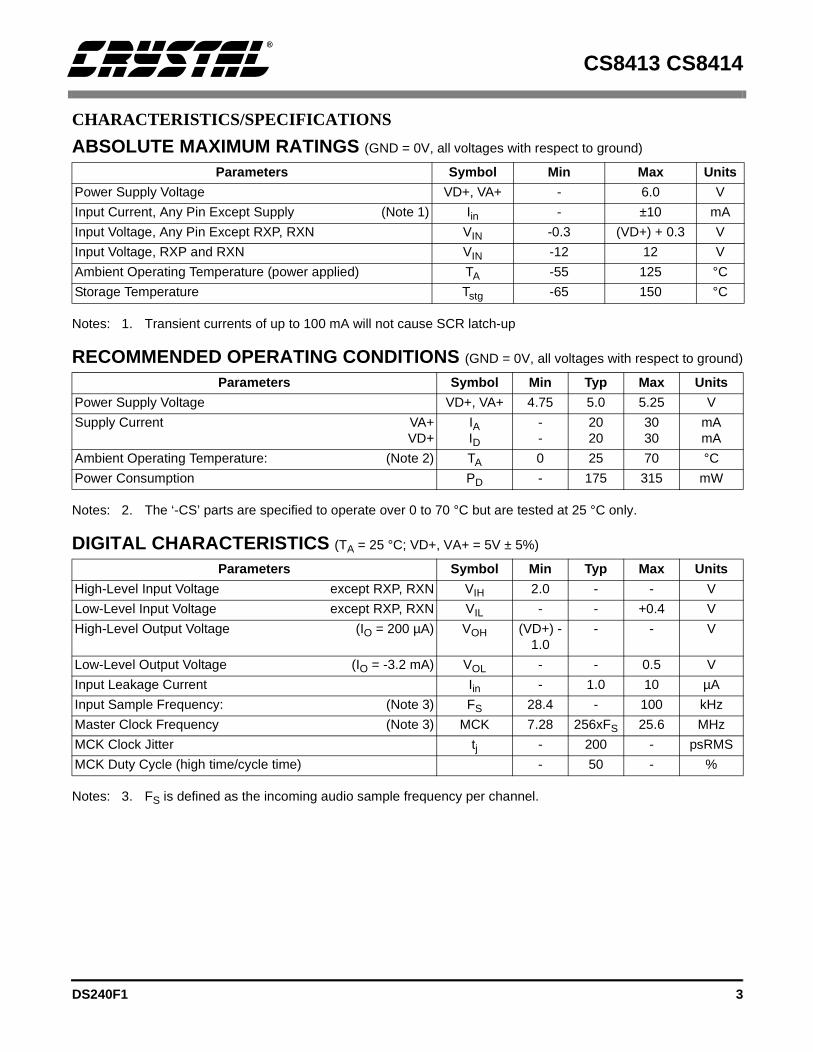
ABSOLUTE MAXIMUM RATINGS (GND = 0V, all voltages with respect to ground)
Notes: 1. Transient currents of up to 100 mA will not cause SCR latch-up
RECOMMENDED OPERATING CONDITIONS (GND = 0V, all voltages with respect to ground)
Notes: 2. The ‘-CS’ parts are specified to operate over 0 to 70 °C but are tested at 25 °C only.
DIGITAL CHARACTERISTICS (TA = 25 °C; VD+, VA+ = 5V ± 5%)
Notes: 3. FS is defined as the incoming audio sample frequency per channel.
Parameters Symbol Min Max Units
Power Supply Voltage VD+, VA+ - 6.0 V
Input Current, Any Pin Except Supply (Note 1) Iin - ±10 mA
Input Voltage, Any Pin Except RXP, RXN VIN -0.3 (VD+) + 0.3 V
Input Voltage, RXP and RXN VIN -12 12 V
Ambient Operating Temperature (power applied) TA -55 125 °C
Storage Temperature Tstg -65 150 °C
Parameters Symbol Min Typ Max Units
Power Supply Voltage VD+, VA+ 4.75 5.0 5.25 V
Supply Current VA+VD+
IAID
--
2020
3030
mAmA
Ambient Operating Temperature: (Note 2) TA 0 25 70 °C
Power Consumption PD - 175 315 mW
Parameters Symbol Min Typ Max Units
High-Level Input Voltage except RXP, RXN VIH 2.0 - - V
Low-Level Input Voltage except RXP, RXN VIL - - +0.4 V
High-Level Output Voltage (IO = 200 µA) VOH (VD+) - 1.0
- - V
Low-Level Output Voltage (IO = -3.2 mA) VOL - - 0.5 V
Input Leakage Current Iin - 1.0 10 µA
Input Sample Frequency: (Note 3) FS 28.4 - 100 kHz
Master Clock Frequency (Note 3) MCK 7.28 256xFS 25.6 MHz
MCK Clock Jitter tj - 200 - psRMS
MCK Duty Cycle (high time/cycle time) - 50 - %
DS240F1 3
CS8413 CS8414
DIGITAL CHARACTERISTICS - RS422 RECEIVERS (RXP, RXN pins only; VD+, VA+ = 5V ± 5%)
Notes: 4. VCM - Input Common Mode Range
5. When the receiver inputs are configured for single ended operation (e.g. consumer configuration) the signal amplitude must exceed 400 mVp-p for the differential voltage on RXP to RXN to exceed 200 mV. This represents twice the minimum signal level of 200 mVp-p specified in CP340/1201 and IEC-958 (which are not RS-422 compliant).
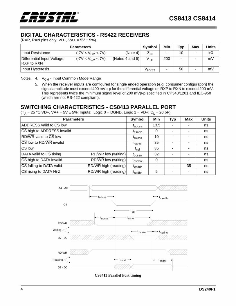
SWITCHING CHARACTERISTICS - CS8413 PARALLEL PORT (TA = 25 °C;VD+, VA+ = 5V ± 5%; Inputs: Logic 0 = DGND, Logic 1 = VD+; CL = 20 pF)
Parameters Symbol Min Typ Max Units
Input Resistance (-7V < VCM < 7V) (Note 4) ZIN - 10 - kΩDifferential Input Voltage, (-7V < VCM < 7V) (Notes 4 and 5)RXP to RXN
VTH 200 - - mV
Input Hysteresis VHYST - 50 - mV
Parameters Symbol Min Typ Max Units
ADDRESS valid to CS low tadcss 13.5 - - ns
CS high to ADDRESS invalid tcsadh 0 - - ns
RD/WR valid to CS low trwcss 10 - - ns
CS low to RD/WR invalid tcsrwi 35 - - ns
CS low tcsl 35 - - ns
DATA valid to CS rising RD/WR low (writing) tdcssw 32 - - ns
CS high to DATA invalid RD/WR low (writing) tcsdhw 0 - - ns
CS falling to DATA valid RD/WR high (reading) tcsddr - - 35 ns
CS rising to DATA Hi-Z RD/WR high (reading) tcsdhr 5 - - ns
A4 - A0
D7 - D0
RD/WR
Writing
Reading
adcsst
csddrt
cslt
dcsswt csdhwt
csdhrt
csadht
CS
D7 - D0
RD/WR
csrwitrwcsst
CS8413 Parallel Port timing
4 DS240F1
CS8413 CS8414
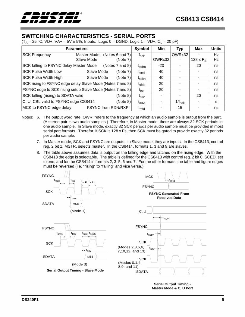
SWITCHING CHARACTERISTICS - SERIAL PORTS (TA = 25 °C; VD+, VA+ = 5V ± 5%; Inputs: Logic 0 = DGND, Logic 1 = VD+; CL = 20 pF)
Notes: 6. The output word rate, OWR, refers to the frequency at which an audio sample is output from the part. (A stereo pair is two audio samples.) Therefore, in Master mode, there are always 32 SCK periods in one audio sample. In Slave mode, exactly 32 SCK periods per audio sample must be provided in most serial port formats. Therefor, if SCK is 128 x Fs, then SCK must be gated to provide exactly 32 periods per audio sample.
7. In Master mode, SCK and FSYNC are outputs. In Slave mode, they are inputs. In the CS8413, control reg. 2 bit 1, MSTR, selects master. In the CS8414, formats 1, 3 and 9 are slaves.
8. The table above assumes data is output on the falling edge and latched on the rising edge. With the CS8413 the edge is selectable. The table is defined for the CS8413 with control reg. 2 bit 0, SCED, set to one, and for the CS8414 in formats 2, 3, 5, 6 and 7. For the other formats, the table and figure edges must be reversed (i.e. “rising” to “falling” and vice versa.)
Parameters Symbol Min Typ Max Units
SCK Frequency Master Mode (Notes 6 and 7)Slave Mode (Note 7)
fsck -OWRx32
OWRx32-
-128 x FS
HzHz
SCK falling to FSYNC delay Master Mode (Notes 7 and 8) tsfdm -20 - 20 ns
SCK Pulse Width Low Slave Mode (Note 7) tsckl 40 - - ns
SCK Pulse Width High Slave Mode (Note 7) tsckh 40 - - ns
SCK rising to FSYNC edge delay Slave Mode (Notes 7 and 8) tsfds 20 - - ns
FSYNC edge to SCK rising setup Slave Mode (Notes 7 and 8) tfss 20 - - ns
SCK falling (rising) to SDATA valid (Note 8) tssv - - 20 ns
C, U, CBL valid to FSYNC edge CS8414 (Note 8) tcuvf - 1/fsck - s
MCK to FSYNC edge delay FSYNC from RXN/RXP tmfd - 15 - ns
sfdst
ssvt
SDATA
SCK
FSYNCfsst
MSB
sckht
ssvt
scklt
SDATA
SCK
FSYNC
MSB
(Mode 1)
(Mode 3)
sfdmt
ssvt
cuvft
SDATA
SCK
FSYNC
C, U
Serial Output Timing - Slave Mode
Serial Output Timing - Master Mode & C, U Port
FSYNC Generated From Received Data
FSYNC
mfdtMCK
fsstsfdst
sckhtscklt
SCK
(Modes 2,3,5,6,7,10,12, and 13)
(Modes 0,1,4,8,9, and 11)
DS240F1 5
CS8413 CS8414
ReceiverCircuit
(See Appendix A)
0.1 µF
+5V Analog +5V Digital
22 70.1 µF5kΩ
21
9
10
20
VA+
AGND
RXP
RXN
FILT
DGND
MCK
FSYNC
SCK
SDATA
ERF
INT
CS
RD/WR
A0-A4
D0-D7
19
1112
26
25
14
24
23
AudioData
Processor
AudioData
Processor
or
Microcontroller
VD+
8
0.068 µF
470 Ω
CS8413
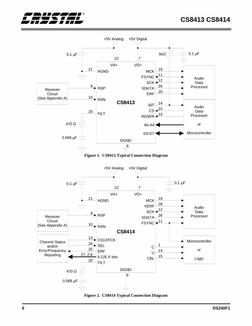
Figure 1. CS8413 Typical Connection Diagram
ReceiverCircuit
(See Appendix A)
0.1 µF
+5V Analog +5V Digital
22 70.1 µF
21
9
10
20
VA+
AGND
RXP
RXN
FILT
DGND
MCK
VERF
SCK
SDATA
FSYNC
C
U
CBL
19
2812
26
11
1
14
AudioData
Processor
Microcontroller
or
Logic
VD+
8
0.068 µF
470 Ω
CS841413
16
2527, 2-6 15
Channel Statusand/or
Error/FrequencyReporting
CS12/FCK
SEL
ERF
6 C/E-F bits
Figure 2. CS8414 Typical Connection Diagram
6 DS240F1
CS8413 CS8414
asstsfalsAeg-
erioted
-.rs,
edpednpr3.
is.
zegns.tae-o is
r,
ion-
al-m.es
GENERAL DESCRIPTION
The CS8413/14 are monolithic CMOS circuits thatreceive and decode audio and digital data accord-ing to the AES/EBU, IEC 958, S/PDIF, and EIAJCP340/1201 interface standards. Both chips con-tain RS422 line receivers and Phase-Locked Loops(PLL) that recover the clock and synchronizationsignals, and de-multiplex the audio and digital data.The CS8413 contains a configurable internal buffermemory, read via a parallel port, which can bufferchannel status, user, and optionally auxiliary data.The CS8414 de-multiplexes the channel status, us-er, and validity information directly to serial outputpins with dedicated pins for the most importantchannel status bits. Both chips also contain exten-sive error reporting as well as incoming sample fre-quency indication for auto-set applications.
The CS8413/14 are pin-compatible with theCS8411/12 digital audio receiver parts. The func-tionality of the CS8413/14 is the same as theCS8411/12 with two exceptions: first, the operat-ing frequency (sample rate) of the CS8413/14 is ex-tended to include 96 kHz, and second, thefrequency reporting bits are modified to delete the±400 ppm ranges, and include 88.2 kHz and96 kHz ranges.
Familiarity with the AES/EBU and IEC 958 speci-fications are assumed throughout this document.The App Note, Overview of Digital Audio Inter-face Data Structures, contains information on digi-tal audio specifications; however, it is not meant tobe a complete reference. To guarantee compliance,the proper standards documents should be ob-tained. The AES/EBU standard, AES3-1985,should be obtained from the Audio EngineeringSociety or ANSI (ANSI document # ANSI S4.40-1985); the IEC 958 standard from the InternationalElectrotechnical Commission; and the EIAJCP340/1201 standard from the Japanese Electron-ics Bureau.
Line Receiver
The RS422 line receiver can decode differentialwell as single ended inputs. The receiver consiof a differential input Schmitt trigger with 50mV ohysteresis. The hysteresis prevents noisy signfrom corrupting the phase detector. Appendix contains more information on how to configure thline receivers for differential and single ended sinals.
Clocks and Jitter Attenuation
The primary function of these chips is to recovaudio data and low jitter clocks from a digital audtransmission line. The clocks that can be generaare MCK (256xFS), SCK (64xFS), and FSYNC (FSor 2xFS). MCK is the output of the voltage controlled oscillator which is a component of the PLLThe PLL consists of phase and frequency detectoa second-order loop filter, and a voltage controlloscillator. All components of the PLL are on chiwith the exception of a resistor and capacitor usin the loop filter. This filter is connected betweethe FILT pin and AGND. The typical closed-lootransfer function, which specifies the PLL’s jitteattenuation characteristics, is shown in Figure Most jitter introduced by the transmission line high in frequency and will be strongly attenuated
Multiple frequency detectors are used to minimithe time it takes the PLL to lock to the incomindata stream and to prevent false lock conditioWhen the PLL is not locked to the incoming dastream, the frequency detectors pull the VCO frquency within the lock range of the PLL. When ndigital audio data is present, the VCO frequencypulled to its minimum value.
As a master, SCK is always MCK divided by fouproducing a frequency of 64xFS. In the CS8413,FSYNC can be programmed to be a divided versof MCK or it can be generated directly from the incoming data stream. In the CS8414, FSYNC is ways generated from the incoming data streaWhen FSYNC is generated from the data, its edg
DS240F1 7
CS8413 CS8414
are extracted at times when intersymbol interfer-ence is at a minimum. This provides a sample fre-quency clock that is as spectrally pure as the digitalaudio source clock for moderate length transmis-sion lines. For long transmission lines, the CS8413can be programmed to generate FSYNC fromMCK instead of from the incoming data.
CS8413 DESCRIPTION
The CS8413 is more flexible than the CS8414 butrequires a microcontroller or DSP to load internalregisters. The CS8414 does not have internal regis-ters so it may be used in a stand-alone mode wherea microprocessor or DSP is not available.
The CS8413 accepts data from a transmission linecoded according to the digital audio interface stan-dards. The I.C. recovers clocks and data, and sepa-rates the audio data from control information. Theaudio data is output through a configurable serialport and the control information is stored in internaldual-port RAM. Extensive error reporting is avail-able via internal registers with the option of repeat-ing the last sample when an error occurs. A blockdiagram of the CS8413 is shown in Figure 4
Parallel Port
The parallel port accesses two status registers, twointerrupt enable registers, two control registers, and28 bytes of dual-port buffer memory. The statusregisters and interrupt enable registers occupy thesame address space. A bit in control register 1 se-lects the two registers, either status or interrupt en-able, that occupy addresses 0 and 1 in the memorymap. The address bus and the RD/WR line shouldbe valid when CS goes low. If RD/WR is low, thevalue on the data bus will be written into the buffermemory at the specified address. If RD/WR is high,the value in the buffer memory, at the specified ad-dress, is placed on the data bus. Detailed timing forthe parallel port can be found in the SwitchingCharacteristics - Parallel Port table.
The memory space on the CS8413 is allocated asshown in Figure 5. There are three defined buffermodes selectable by two bits in control register 1.Further information on the buffer modes can befound in the Control Registers section.
102
103
104
105
106
-30
-25
-20
-15
-10
-5
0
5
Jitter Frequency (Hz)
Jitte
rA
ttenu
atio
n(d
B)
Figure 3. Typical Jitter Attenuation Characteristics
8 DS240F1
CS8413 CS8414
Status and IEnable Registers
The status and interrupt enable registers occupy thesame address space. The IER/SR bit in control reg-ister 1 selects whether the status registers(IER/SR = 0) or the IEnable registers (IER/SR = 1)occupy addresses 0 and 1. Upon power-up, the con-trol and IEnable registers contain all zeros; there-fore, the status registers are visible and allinterrupts are disabled. The IER/SR bit must be setto make the IEnable registers visible.
Status register 1 (SR1), shown in Figure 6, reportsall the conditions that can generate a low pulse fourSCLK cycles wide on the interrupt pin (INT). Thethree least significant bits, FLAG2-FLAG0, are
used to monitor the ram buffer. These bits continu-ally change and indicate the position of the bufferpointer which points to the buffer memory locationcurrently being written. Each flag has a corre-sponding interrupt enable bit in IEnable register 1which, when set, allows a transition on the flag togenerate a pulse on the interrupt pin. FLAG0 andFLAG1 cause interrupts on both edges whereasFLAG2 causes an interrupt on the rising edge only.Further information, including timing, on the flagscan be found in the Buffer Memory section.
The next five bits; ERF, SLIP, CCHG,CRCE/CRC1, and CSDIF/CRC2, are latcheswhich are set when their corresponding conditionsoccur, and are reset when SR1 is read. Interrupt
RXP
RXN
VD+
DGND
VA+ FILT AGND MCK
FSYNC
SCK
SDATA
INT
ERF
CS
RD/WR
A4/FCK
A0-A3
D0-D7
9
10
7
8
22 20 21 19
11
12
26
14
25
24
23
134 8
Clock & DataRecovery
Bi-phaseDecoder
De-Multiplexor
crccheck
AudioSerialPort
ControlRegisters
2 X 8
BufferMemory28 X 8
IEnable&
Status4 X 8
aux
user
C.S.
slipped
parity
validity
crc
coding
no lock
FrequencyComparator
Figure 4. CS8413 Block Diagram
DS240F1 9
CS8413 CS8414
partednytheff-sta-by-re ishe,nndndct-
el.hede
ed,d
E,nd-,2
d-rupt Ain
pulses are generated the first time that condition oc-curs. If the status register is not read, further in-stances of that same condition will not generateanother interrupt. ERF is the error flag bit and is setwhen the ERF pin goes high. It is an OR’ing of theerrors listed in status register 2, bits 0 through 4,AND’ed with their associated interrupt enable bitsin IEnable register 2.
SLIP is only valid when the audio port is in slavemode (FSYNC and SCK are inputs to the CS8413).This flag is set when an audio sample is dropped or
reread because the audio data output from the is at a different frequency than the data receivfrom the transmission line. CCHG is set when abit in channel status bytes 0 through 3, stored in buffer, changes from one block to the next. In buer modes 0 and 1, only one channel of channel tus data is buffered, so CCHG is only affected that channel. (CS2/CS1 in CR1 selects which channel is buffered.) In buffer mode 2 both channels abuffered, so both channels affect CCHG. This bitupdated after each byte (0 to 3) is written to tbuffer. The two most significant bits in SR1CRCE/CRC1 and CSDIF/CRC2, are dual functioflags. In buffer modes 0 and 1, they are CRCE aCSDIF, and in buffer mode 2, they are CRC1 aCRC2. In buffer modes 0 and 1, the channel seleed by the CS2/CS1 bit is stored in RAM and CRCEindicates that a CRC error occurred in that channCSDIF is set if there is any difference between tchannel status bits of each channel. In buffer mo2 channel status from both channels is bufferwith CRC1 indicating a CRC error in channel 1 anCRC2 indicating a CRC error in channel 2. CRCCRC1, and CRC2 are updated at the block bouary. Block boundary violations also cause CRC1or CRCE to be set.
IEnable register 1, which occupies the same adress space as status register 1, contains interenable bits for all conditions in status register 1.“1” in a bit location enables the same bit location
0 1 2 3
User Data
1st FourBytes of
C. S. Data
1st FourBytes of
C. S. Data
1st FourBytes ofLeft C. S.
Data
AuxiliaryData
Last20 BytesChannelStatusData
Status 1 / IEnable 1
C. S.Data
LeftC. S.Data
RightC. S.Data
1st FourBytes of
RightC. S. Data
UNDEFINED
ADDRESS
Memory Mode
0
12
3
45
6
78
9A
B
C
D
E
F
10
11
12
13
1415
16
17
18
19
1A
1B
1C1D
1E1F
Control Register 1
Control Register 2
Status 2 / IEnable 2
Figure 5. CS8413 Buffer Memory Map
SR1: CSDIF: CS different between sub-frames. Buffer modes 0 & 1CRC2: CRC Error - sub-frame 2. Buffer mode 2 only.CRCE: CRC Error - selected sub-frame. Buffer modes 0 & 1CRC1: CRC Error - sub-frame 1. Buffer mode 2 only.CCHG: Channel Status changedSLIP: Slipped an audio sampleERF: Error Flag. ORing of all errors in SR2.FLAG2: High for first four bytes of channel statusFLAG1: Memory mode dependent - See Figure 11.FLAG0: High for last two bytes of user data.
IER1: Enables the corresponding bit in SR1.A “1” enables the interrupt. A “0” masks the interrupt.
X:00 7 6 5 4 3 2 1 0
SR1. CSDIF/CRC2
CRCE/CRC1
CCHG SLIP ERF FLAG2 FLAG1 FLAG0
IER1. INTERRUPT ENABLE BITS FOR ABOVE
Figure 6. Status/IEnable Register 1
SR1: CSDIF: CS different between sub-frames. Buffer modes 0 & 1CRC2: CRC Error - sub-frame 2. Buffer mode 2 only.CRCE: CRC Error - selected sub-frame. Buffer modes 0 & 1CRC1: CRC Error - sub-frame 1. Buffer mode 2 only.CCHG: Channel Status changedSLIP: Slipped an audio sampleERF: Error Flag. ORing of all errors in SR2.FLAG2: High for first four bytes of channel statusFLAG1: Memory mode dependent - See Figure 11.FLAG0: High for last two bytes of user data.
IER1: Enables the corresponding bit in SR1.A “1” enables the interrupt. A “0” masks the interrupt.
X:00 7 6 5 4 3 2 1 0
SR1. CSDIF/CRC2
CRCE/CRC1
CCHG SLIP ERF FLAG2 FLAG1 FLAG0
IER1. INTERRUPT ENABLE BITS FOR ABOVE
10 DS240F1
CS8413 CS8414
an isin ise
etrgeses
al-eLL
n-sileitsryhisow-
rolvelss
hte-
s a
status register 1 to generate an interrupt pulse. A“0” masks that particular status bit from causing aninterrupt.
Status register 2 (SR2) reports all the conditionsthat can affect the error flag bit in SR1 and the errorpin (ERF), and can specify the received clock fre-quency. As previously mentioned, the first five bitsof SR2 are AND’ed with their interrupt enable bits(in IER2) and then OR’ed to create ERF. The V,PARITY, CODE and LOCK bits are latches whichare set when their corresponding conditions occur,and are reset when SR2 is read. The ERF pin is as-serted each time the error occurs assuming the in-terrupt enable bit in IER2 is set for that particularerror. When the ERF pin is asserted, the ERF bit inSR1 is set. If the ERF bit was not set prior to theERF pin assertion, an interrupt will be generated(assuming bit 3 in IER1 is set). Although the ERFpin is asserted for each occurrence of an enabled er-ror condition, the ERF bit will only cause an inter-rupt once if SR1 is not read.
V is the validity status bit which is set any time thereceived validity bit is high. PARITY is set when aparity error is detected. CODE is set when a bi-phase coding error is detected. LOCK is assertedwhen the receiver PLL is not locked and occurswhen there is no input on RXP/RXN, or if the re-ceived frequency is out of the receiver lock range(28.4 kHz to 100 kHz).
The upper three bits in SR2, FREQ2-FREQ0, creport the receiver frequency when the receiverlocked. These bits are only valid when FCEN control register 1 is set, and a 6.144 MHz clockapplied to the FCK pin. When FCEN is set, thA4/FCK pin is used as FCK and A4 is internally sto zero; therefore, only the lower half of the buffecan be accessed. Table 1 lists the frequency ranreported. The FREQ bits are updated three timper block and the clock on the FCK pin must be vid for two thirds of a block for the FREQ bits to baccurate. The FREQ bits are invalid when the Pis out of lock.
Table 1. Incoming Sample Frequency BitsIEnable register 2 has corresponding interrupt eable bits for the first five bits in SR2. A “1” enablethe condition in SR2 to cause ERF to go high, wha “0” masks that condition. Bit 5 is unused and b6 and 7, the two most significant bits, are factotest bits and must be set to zero when writing to tregister. The CS8413 sets these bits to zero on per-up.
Control Registers
The CS8413 contains two control registers. Contregister 1 (CR1), at address 2, selects system lefeatures, while control register 2 (CR2), at addre3, configures the audio serial port.
In control register 1, when RST is low, all outputsare reset except MCK (FSYNC and SCLK are higimpedance). The CS8413 should be reset imedialy after power-up and any time the user perform
SR2: FREQ2: The 3 FREQ bits indicate incoming sample frequency.FREQ1: (must have 6.144 MHz clock on FCK pin and FCENFREQ0: must be “1”)LOCK: Out-of-Lock errorCODE: Coding violationPARITY: Parity errorV: Validity bit high
IER2: TEST1,0: (0 on power-up) Must stay at “0”.INT. ENABLES: Enables the corresponding bit in SR2.
A “1” enables the interrupt. A “0” masks the interrupt.
X:01 7 6 5 4 3 2 1 0
SR2. FREQ2 FREQ1 FREQ0 Reserved LOCK CODE PARITY V
IER2. TEST1 TEST0 INT. ENABLE BITS FOR ABOVE
Figure 7. Status/IEnable Register 2
FREQ2 FREQ1 FREQ0 Sample Frequency
0 0 0 Out of Range
0 0 1 reserved
0 1 0 reserved
0 1 1 96 kHz ± 4%
1 0 0 88.2 kHz ± 4%
1 0 1 48 kHz ± 4%
1 1 0 44.1 kHz ± 4%
1 1 1 32 kHz ± 4%
DS240F1 11
CS8413 CS8414
system-wide reset. After the user sets RST high, theCS8413 comes fully out of reset when the blockboundary is found. The serial port, in master mode,will begin to operate as soon as RST goes high. B0and B1 select one of three buffer modes listed inTable and illustrated in Figure 5. In all modes fourbytes of user data are stored. In mode 0, one entireblock of channel status is stored. In mode 1 eightbytes of channel status and sixteen bytes of auxilia-ry data are stored. In mode 2, eight bytes of channelstatus from each sub-frame are stored. The buffermodes are discussed in more detail in the BufferMemory section. The next bit, CS2/CS1, selects theparticular sub-frame of channel status to buffer inmodes 0 and 1, and has no effect in mode 2. WhenCS2/CS1 is low, sub-frame 1 is buffered, and whenCS2/CS1 is high, sub-frame 2 is buffered. IER/SRselects which set of registers, either IEnable or sta-tus, occupy addresses 0 and 1. When IER/SR islow, the status registers occupy the first two ad-dresses, and when IER/SR is high, the IEnable reg-isters occupy those addresses. FCEN enables theinternal frequency counter. A 6.144 MHz clockmust be connected to the FCK pin as a reference.The value of the FREQ bits in SR2 are not valid un-til two thirds of a block of data is received. SinceFCK and A4, the most significant address bit, oc-cupy the same pin, A4 is internally set to zero whenFCEN is high. Since A4 is forced to zero, the upperhalf of the buffer is not accessible while using thefrequency compare feature. FPLL determines howFSYNC is derived. When FPLL is low, FSYNC isderived from the incoming data, and when FPLL ishigh, it is derived from the internal phase-lockedloop.
Control Register 2 configures the serial port whichconsists of three pins: SCK, SDATA, and FSYNC.SDATA is always an output, but SCK and FSYNCcan be configured as inputs or outputs. FSYNC andSDATA can have a variety of relationships to eachother, and the polarity of SCK can be controlled.The large variety of audio data formats provides an
easy interface to most DSPs and other audio pro-cessors. SDATA is normally just audio data, butspecial modes are provided that output received bi-phase data, or received NRZ data with zeros substi-tuted for preamble. Another special mode allows anasynchronous SCK input to read audio data fromthe serial port without slipping samples. In thismode FSYNC and SDATA are outputs synchro-nized to the SCK input. Since SCK is asynchronousto the received clock, the number of SCK cyclesbetween FSYNC edges will vary.
ROER, when set, causes the last audio sample to bereread if the error pin, ERF, is active. When out oflock, the CS8413 will output zeros if ROER is set
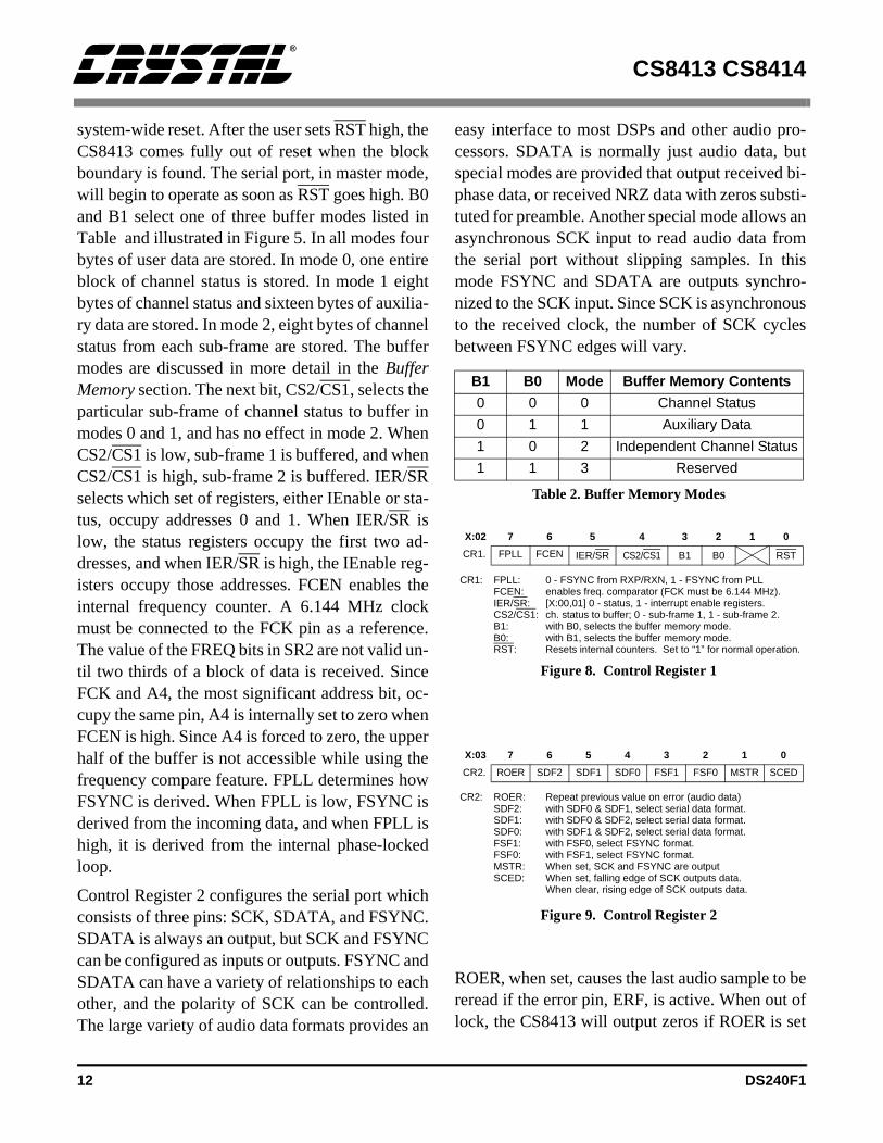
B1 B0 Mode Buffer Memory Contents
0 0 0 Channel Status
0 1 1 Auxiliary Data
1 0 2 Independent Channel Status
1 1 3 Reserved
Table 2. Buffer Memory Modes
CR1: FPLL: 0 - FSYNC from RXP/RXN, 1 - FSYNC from PLLFCEN: enables freq. comparator (FCK must be 6.144 MHz).IER/SR: [X:00,01] 0 - status, 1 - interrupt enable registers.CS2/CS1: ch. status to buffer; 0 - sub-frame 1, 1 - sub-frame 2.B1: with B0, selects the buffer memory mode.B0: with B1, selects the buffer memory mode.RST: Resets internal counters. Set to “1” for normal operation.
X:02 7 6 5 4 3 2 1 0
CR1. FPLL FCEN IER/SR CS2/CS1 B1 B0 RST
Figure 8. Control Register 1
CR2: ROER: Repeat previous value on error (audio data)SDF2: with SDF0 & SDF1, select serial data format.SDF1: with SDF0 & SDF2, select serial data format.SDF0: with SDF1 & SDF2, select serial data format.FSF1: with FSF0, select FSYNC format.FSF0: with FSF1, select FSYNC format.MSTR: When set, SCK and FSYNC are outputSCED: When set, falling edge of SCK outputs data.
When clear, rising edge of SCK outputs data.
X:03 7 6 5 4 3 2 1 0
CR2. ROER SDF2 SDF1 SDF0 FSF1 FSF0 MSTR SCED
Figure 9. Control Register 2
12 DS240F1
CS8413 CS8414
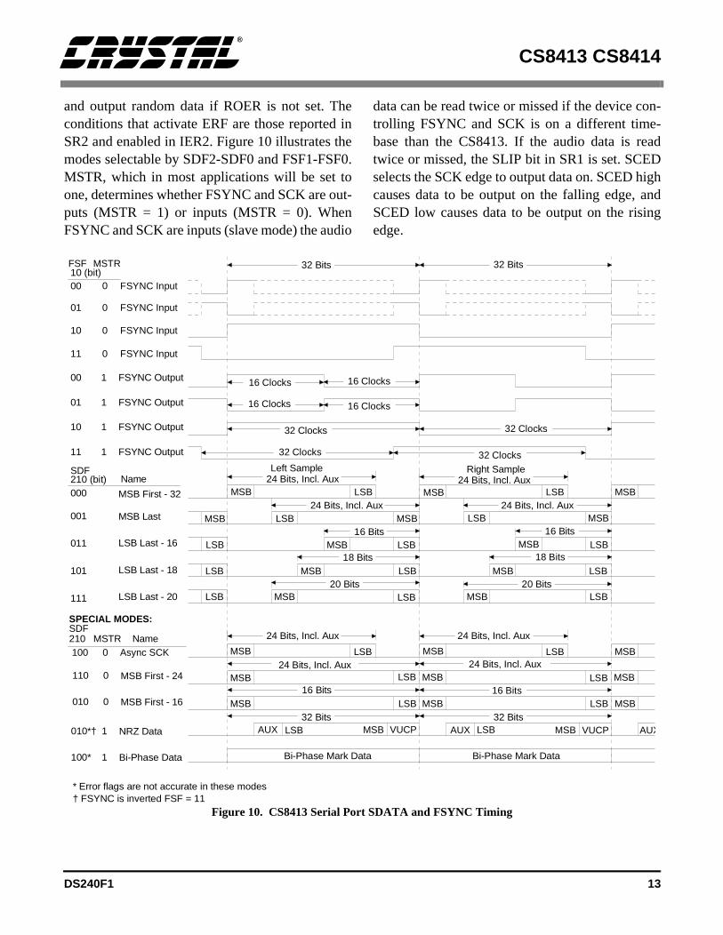
and output random data if ROER is not set. Theconditions that activate ERF are those reported inSR2 and enabled in IER2. Figure 10 illustrates themodes selectable by SDF2-SDF0 and FSF1-FSF0.MSTR, which in most applications will be set toone, determines whether FSYNC and SCK are out-puts (MSTR = 1) or inputs (MSTR = 0). WhenFSYNC and SCK are inputs (slave mode) the audio
data can be read twice or missed if the device con-trolling FSYNC and SCK is on a different time-base than the CS8413. If the audio data is readtwice or missed, the SLIP bit in SR1 is set. SCEDselects the SCK edge to output data on. SCED highcauses data to be output on the falling edge, andSCED low causes data to be output on the risingedge.
24 Bits, Incl. Aux
16 Clocks 16 Clocks
16 Clocks 16 Clocks
32 Clocks
32 Clocks 32 Clocks
32 Clocks
00
01
10
11
1
1
1
1
FSYNC Output
FSYNC Output
FSYNC Output
FSYNC Output
FSF
00
01
10
11
MSTR
0
0
0
0
FSYNC Input
FSYNC Input
FSYNC Input
FSYNC Input
10 (bit)
000 MSB First - 32
001
011
101
111
MSB Last
LSB Last - 16
LSB Last - 18
LSB Last - 20
210 (bit) NameSDF
20 BitsLSB MSB LSB MSB LSB
LSB LSBMSB LSBMSB
LSB LSBMSB LSBMSB
MSB LSB MSB LSB MSB16 Bits
18 Bits
20 Bits
18 Bits
16 Bits
MSB LSB MSB LSB MSB
Left Sample Right Sample
32 Bits 32 Bits
SPECIAL MODES:
* Error flags are not accurate in these modes† FSYNC is inverted FSF = 11
MSB LSB MSB LSB MSB
16 Bits16 BitsMSB MSB MSBLSBLSB
MSB MSB MSBLSBLSB
Bi-Phase Mark DataBi-Phase Mark Data
32 Bits 32 BitsLSB VUCPMSBAUX LSBAUX VUCPMSB AUX
210 MSTR NameSDF
110 0 MSB First - 24
010 0 MSB First - 16
010*† 1 NRZ Data
100* 1 Bi-Phase Data
100 Async SCK0
24 Bits, Incl. Aux 24 Bits, Incl. Aux
24 Bits, Incl. Aux 24 Bits, Incl. Aux
24 Bits, Incl. Aux 24 Bits, Incl. Aux
24 Bits, Incl. Aux
Figure 10. CS8413 Serial Port SDATA and FSYNC Timing
DS240F1 13
CS8413 CS8414
Audio Serial Port
The audio serial port outputs the audio data portionfrom the received data and consists of three pins:SCK, SDATA, and FSYNC. SCK clocks the dataout on the SDATA line. The edge that SCK uses tooutput data is programmable from CR2. FSYNCdelineates the audio samples and may indicate theparticular channel, left or right. Figure 10 illus-trates the multitude of formats that SDATA andFSYNC can take.
Normal Modes
SCK and FSYNC can be inputs (MSTR = 0) or out-puts (MSTR = 1), and are usually programmed asoutputs. As outputs, SCK contains 32 periods foreach sample and FSYNC has four formats. Thefirst two output formats of FSYNC (shown in Fig-ure 10) delineate each word and the identificationof the particular channel must be kept track of ex-ternally. This may be done using the rising edge ofFLAG2 to indicate the next data word is left chan-nel data. The last two output formats of FSYNCalso delineate each channel with the polarity ofFSYNC indicating the particular channel. The lastformat has FSYNC change one SCK cycle beforethe frame containing the data and may be used togenerate an I2S compatible interface.
When SCK is programmed as an input, 32 SCK cy-cles per sample must be provided. (There are twoformats in the Special Modes section where SCKcan have 16 or 24 clocks per sample.) The fourmodes where FSYNC is an input are similar to theFSYNC output modes. The first two require a tran-sition of FSYNC to start the sample frame, whereasthe last two are identical to the correspondingFSYNC output modes. If the circuit generatingSCK and FSYNC is not locked to the master clockof the CS8413, the serial port will eventually be re-read or a sample will be missed. When this occurs,the SLIP bit in SR1 will be set.
SDATA can take on five formats in the normal se-rial port modes. The first format (see Figure 10),MSB First, has the MSB aligned with the start of asample frame. Twenty-four audio bits are outputincluding the auxiliary bits. This mode is compati-ble with many DSPs. If the auxiliary bits are usedfor something other than audio data, they must bemasked off. The second format, MSB Last, outputsdata LSB first with the MSB aligned to the end ofthe sample frame. This format is conducive to seri-al arithmetic. Both of the above formats output allaudio bits from the received data. The last three for-mats are LSB Last formats that output the most sig-nificant 16, 18, and 20 bits respectively, with theLSB aligned to the end of the sample frame. Theseformats are used by many interpolation filters.
Special Modes
Five special modes are included for unique applica-tions. In these modes, the master bit, MSTR, mustbe defined as shown in Figure 10. In the first mode,Asynchronous SCK, FSYNC (which is an output inthis mode) is aligned to the incoming SCK. Thismode is useful when the SCK is locked to an exter-nal event and cannot be derived from MCK. SinceSCK is asynchronous, the number of SCK cyclesper sample frame will vary. The data output will beMSB first, 24 bits, and aligned to the beginning ofa sample frame. The second and third specialmodes are unique in that they contain 24 and 16SCK cycles respectively per sample frame, where-as all normal modes contain 32 SCK cycles. Inthese two modes, the data is MSB first and fills theentire frame. The fourth special mode outputs NRZdata including the V, U, C, and P bits and the pre-amble replaced with zeros. SCK is an output with32 SCK cycles per sample frame. The fifth modeoutputs the biphase data recovered from the trans-mission line with 64 SCK cycles output per sampleframe, with data changing on the rising edge.
Normally, data recovered by the CS8413 is delayedby two frames in propagating through the part, but
14 DS240F1
CS8413 CS8414
in the fourth and fifth special modes, the data is de-layed only a few bit periods before being output.However, error codes, and the C, U and V bits fol-low the normal pathway with a two frame delay (sothat the error code would be output with the offend-ing data in the other modes). As a result, in specialmodes four and five, the error codes are nearly twoframes behind the data output on SDATA.
Buffer Memory
In all buffer modes, the status, mask, and controlregisters are located at addresses 0-3, and the userdata is buffered at locations 4 through 7. The paral-lel port can access any location in the user databuffer at any time; however, care should be takennot to read a location when that location is beingupdated internally. This internal writing is donethrough a second port of the buffer and is done in acyclic manner. As data is received, the bits are as-sembled in an internal 8-bit shift register which,when full, is loaded into the buffer memory. Thefirst bit received is stored in D0 and, after D7 is re-ceived, the byte is written into the proper buffermemory location.
The user data is received one bit per sub-frame. Atthe channel status block boundary, the internalpointer for writing user data is initialized to 04H(Hex). After receiving eight user bits, the byte iswritten to the address indicated by the user pointerwhich is then incremented to point to the next ad-dress. After receiving all four bytes of user data, 32audio samples, the user pointer is set to 04H againand the cycle repeats. FLAG0, in SR1 can be usedto monitor the user data buffer. When the last byteof the user buffer, location 07H, is written, FLAG0is set low and when the second byte, location 05H,is written, FLAG0 is set high. If the correspondingbit in the interrupt enable register (IER1, bit 0) isset, a transition of FLAG0 will generate a low pulseon the interrupt pin. The level of FLAG0 indicates
which two bytes the part will write next, thereby in-dicating which two bytes are free to be read.
FLAG1 is buffer mode dependent and is discussedin the individual buffer mode sections. A transitionof FLAG1 will generate an interrupt if the appro-priate interrupt enable bit is set.
FLAG2 is set high after channel status byte 23, thelast byte of the block, is written and set low afterchannel status byte 3 is written to the buffer mem-ory. FLAG2 is unique in that only the rising edgecan cause an interrupt if the appropriate interruptenable bit in IER1 is set.
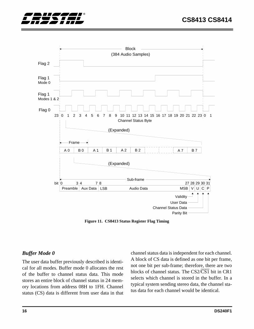
Figure 11 illustrates the flag timing for an entirechannel status block which includes 24 bytes ofchannel status data per channel and 384 audio sam-ples. The lower portion of Figure 11 expands thefirst byte of channel status showing eight pairs ofdata, with a pair defined as a frame. This is furtherexpanded showing the first sub-frame (A0) to con-tain 32 bits defined as per the digital audio stan-dards. When receiving stereo, channel A is left andchannel B is right.
For all three buffer modes, the three most signifi-cant bits in SR1, shown in Figure 6, can be used tomonitor the channel status data. In buffer mode 2,bits 7 and 6 change definition and are described inthat section. Channel status data, as described in thestandards, is independent for each channel. Eachchannel contains its own block of channel statusdata, and in most systems, both channels will con-tain the same channel status data. Buffer modes 0and 1 operate on one block of channel status withthe particular block selected by the CS2/CS1 bit inCR1. CSDIF, bit 7 in SR1, indicates when thechannel status data for each channel is not the sameeven though only one channel is being buffered.CRCE, bit 6 in SR1, indicates a CRC error oc-curred in the buffered channel. CCHG, bit 5 inSR1, is set when any bit in the buffered channel sta-tus bytes 0 to 3, change from one block to the next.
DS240F1 15
CS8413 CS8414
Buffer Mode 0
The user data buffer previously described is identi-cal for all modes. Buffer mode 0 allocates the restof the buffer to channel status data. This modestores an entire block of channel status in 24 mem-ory locations from address 08H to 1FH. Channelstatus (CS) data is different from user data in that
channel status data is independent for each channel.A block of CS data is defined as one bit per frame,not one bit per sub-frame; therefore, there are twoblocks of channel status. The CS2/CS1 bit in CR1selects which channel is stored in the buffer. In atypical system sending stereo data, the channel sta-tus data for each channel would be identical.
Flag 0
Flag 1Mode 0
Flag 1Modes 1 & 2
Flag 2
B 0A 0 B 1A 1 B 2A 2 B 7A 7
Aux Data0 3 4 7
LSB8
Audio DataPreamble28 29 30 31V U C PMSB
27
(384 Audio Samples)
23 0 1 2 3 4 5 6 7 8 9 10 11 12 13 14 15 16 17 18 19 20 21 22 23 0 1Channel Status Byte
(Expanded)
(Expanded)
bit
Frame
Sub-frame
Block
Validity
User DataChannel Status Data
Parity Bit
Figure 11. CS8413 Status Register Flag Timing
16 DS240F1
CS8413 CS8414
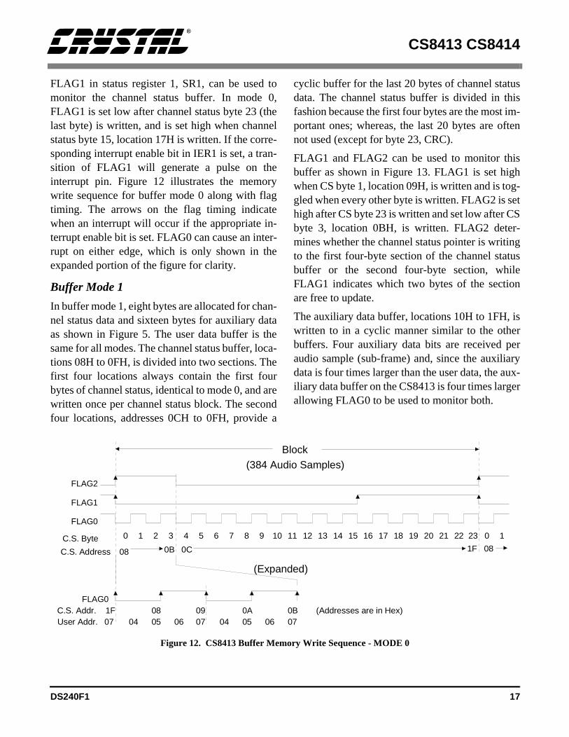
FLAG1 in status register 1, SR1, can be used tomonitor the channel status buffer. In mode 0,FLAG1 is set low after channel status byte 23 (thelast byte) is written, and is set high when channelstatus byte 15, location 17H is written. If the corre-sponding interrupt enable bit in IER1 is set, a tran-sition of FLAG1 will generate a pulse on theinterrupt pin. Figure 12 illustrates the memorywrite sequence for buffer mode 0 along with flagtiming. The arrows on the flag timing indicatewhen an interrupt will occur if the appropriate in-terrupt enable bit is set. FLAG0 can cause an inter-rupt on either edge, which is only shown in theexpanded portion of the figure for clarity.
Buffer Mode 1
In buffer mode 1, eight bytes are allocated for chan-nel status data and sixteen bytes for auxiliary dataas shown in Figure 5. The user data buffer is thesame for all modes. The channel status buffer, loca-tions 08H to 0FH, is divided into two sections. Thefirst four locations always contain the first fourbytes of channel status, identical to mode 0, and arewritten once per channel status block. The secondfour locations, addresses 0CH to 0FH, provide a
cyclic buffer for the last 20 bytes of channel statusdata. The channel status buffer is divided in thisfashion because the first four bytes are the most im-portant ones; whereas, the last 20 bytes are oftennot used (except for byte 23, CRC).
FLAG1 and FLAG2 can be used to monitor thisbuffer as shown in Figure 13. FLAG1 is set highwhen CS byte 1, location 09H, is written and is tog-gled when every other byte is written. FLAG2 is sethigh after CS byte 23 is written and set low after CSbyte 3, location 0BH, is written. FLAG2 deter-mines whether the channel status pointer is writingto the first four-byte section of the channel statusbuffer or the second four-byte section, whileFLAG1 indicates which two bytes of the sectionare free to update.
The auxiliary data buffer, locations 10H to 1FH, iswritten to in a cyclic manner similar to the otherbuffers. Four auxiliary data bits are received peraudio sample (sub-frame) and, since the auxiliarydata is four times larger than the user data, the aux-iliary data buffer on the CS8413 is four times largerallowing FLAG0 to be used to monitor both.
FLAG0
FLAG1
FLAG2
(384 Audio Samples)
(Expanded)
Block
08 0B 0C 1F 08C.S. Address
0 1 2 3 4 5 6 7 8 9 10 11 12 13 14 15 16 17 18 19 20 21 22 23 0 1C.S. Byte
FLAG0C.S. Addr.User Addr.
(Addresses are in Hex)04 05 06 07 04 05 06 07
08 09 0A 0B1F07
Figure 12. CS8413 Buffer Memory Write Sequence - MODE 0
DS240F1 17

CS8413 CS8414
Buffer Mode 2
In buffer mode 2, two 8-byte buffers are availableto independently buffer each channel of channelstatus data. Both buffers are identical to the channelstatus buffer in mode 1 and are written to simulta-
neously, with locations 08H to 0FH containing CSdata for channel A and locations 10H to 17H con-taining CS data for channel B. Both CS buffers canbe monitored using FLAG1 and FLAG2 as de-scribed in the BUFFER MODE 1 section.
FLAG0
FLAG1
FLAG2
(384 Audio Samples)
(Expanded)
Block
08 0B 0C 0F 08C.S. Address
0 1 2 3 4 5 6 7 8 9 10 11 12 13 14 15 16 17 18 19 20 21 22 23 0 1C.S. Byte
FLAG0C.S. Addr.
User Addr.
(Addresses are in Hex)
0F 0C 0F 0C 0F 0C 0F 0C
FLAG1
Aux. Addr.
08 09 0A 0B
04 05 06 07 04 05 06 0707
0F
10 13,14 17 18 1B,1C 1F 10 13,14 17 18 1B,1C 1F1F
Figure 13. CS8413 Buffer Memory Write Sequence - MODE 1
FLAG0
FLAG1
FLAG2
(384 Audio Samples)Block
Left C.S. Ad.
0 1 2 3 4 5 6 7 8 9 10 11 12 13 14 15 16 17 18 19 20 21 22 23 0 1C.S. Byte
(Addresses are in Hex)(Expanded)
FLAG0Left C.S. Ad.
User Address
08 0B 0C 0F 080F 0C 0F 0C 0F 0C 0F 0C
10 13 14 17 1017 14 17 14 17 14 17 14Right C.S. Ad.
Right C.S. Ad.
FLAG1
05 06 07 04 05 06 0704
08 09 0A 0B10 11 12 13
Figure 14. CS8413 Buffer Memory Write Sequence - MODE 2
18 DS240F1
CS8413 CS8414
4heC
tori--d
in-
ngm ofle. in
or-h isnisis
The two most significant bits in SR1 change defini-tion for buffer mode 2. These two bits, when set, in-dicate CRC errors for their respective channels. ACRC error occurs when the internal calculatedCRC for channel status bytes 0 through 22 does notmatch channel status byte 23. CCHG, bit 5 in SR1,is set when any bit in the first four channel statusbytes of either channel changes from one block tothe next. Since channel status doesn’t change veryoften, this bit may be monitored rather than check-ing all the bits in the first four bytes. These bits areillustrated in Figure 6.
Buffer Updates and Interrupt Timing
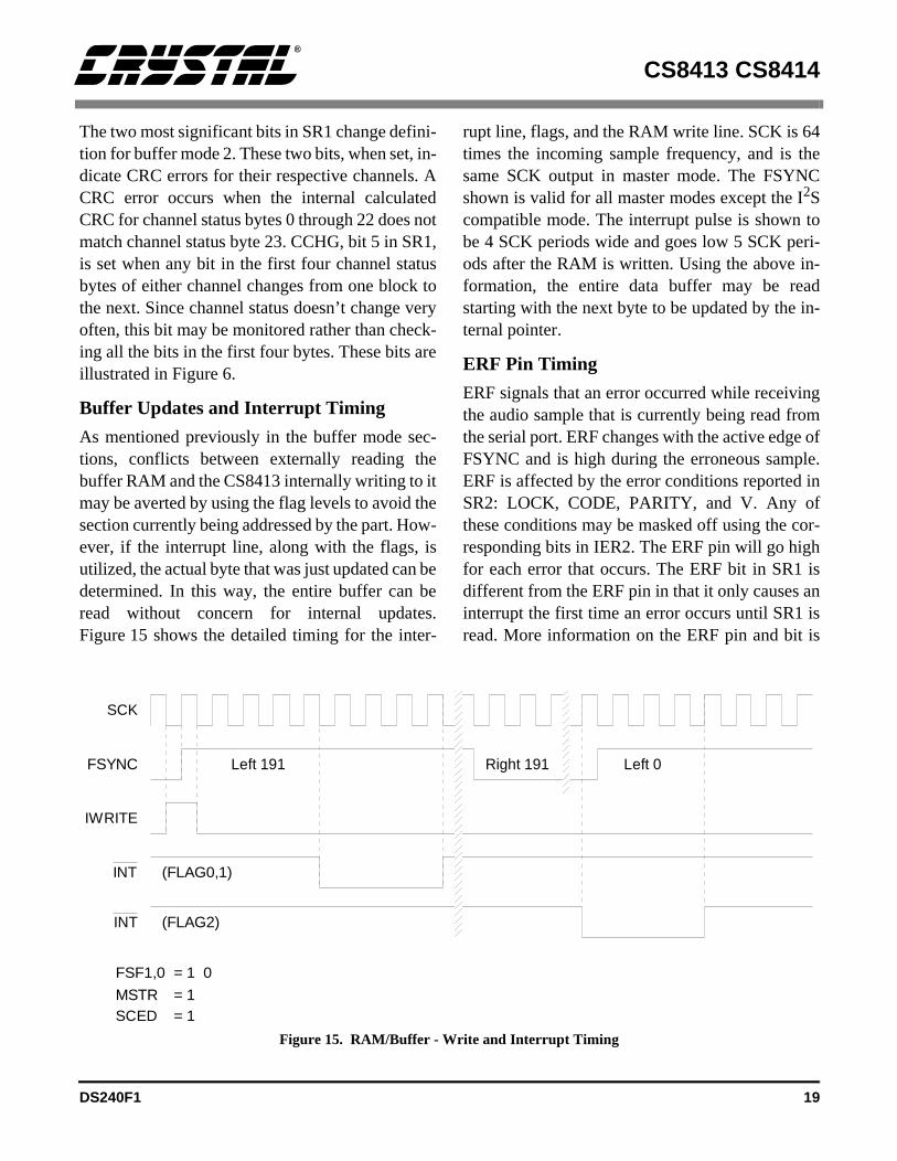
As mentioned previously in the buffer mode sec-tions, conflicts between externally reading thebuffer RAM and the CS8413 internally writing to itmay be averted by using the flag levels to avoid thesection currently being addressed by the part. How-ever, if the interrupt line, along with the flags, isutilized, the actual byte that was just updated can bedetermined. In this way, the entire buffer can beread without concern for internal updates.Figure 15 shows the detailed timing for the inter-
rupt line, flags, and the RAM write line. SCK is 6times the incoming sample frequency, and is tsame SCK output in master mode. The FSYNshown is valid for all master modes except the I2Scompatible mode. The interrupt pulse is shownbe 4 SCK periods wide and goes low 5 SCK peods after the RAM is written. Using the above information, the entire data buffer may be reastarting with the next byte to be updated by the ternal pointer.
ERF Pin Timing
ERF signals that an error occurred while receivithe audio sample that is currently being read frothe serial port. ERF changes with the active edgeFSYNC and is high during the erroneous sampERF is affected by the error conditions reportedSR2: LOCK, CODE, PARITY, and V. Any ofthese conditions may be masked off using the cresponding bits in IER2. The ERF pin will go higfor each error that occurs. The ERF bit in SR1different from the ERF pin in that it only causes ainterrupt the first time an error occurs until SR1 read. More information on the ERF pin and bit
FSYNC
(FLAG0,1)
(FLAG2)
SCK
Left 191 Right 191 Left 0
INT
IWRITE
INT
FSF1,0
MSTRSCED = 1
= 1
= 1 0
Figure 15. RAM/Buffer - Write and Interrupt Timing
DS240F1 19
CS8413 CS8414
,d.ate
e-eet.
u-C,ur-ix
contained at the end of the Status and IEnable Reg-isters section.
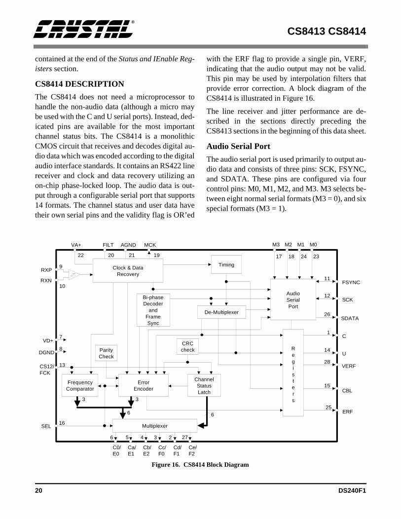
CS8414 DESCRIPTION
The CS8414 does not need a microprocessor tohandle the non-audio data (although a micro maybe used with the C and U serial ports). Instead, ded-icated pins are available for the most importantchannel status bits. The CS8414 is a monolithicCMOS circuit that receives and decodes digital au-dio data which was encoded according to the digitalaudio interface standards. It contains an RS422 linereceiver and clock and data recovery utilizing anon-chip phase-locked loop. The audio data is out-put through a configurable serial port that supports14 formats. The channel status and user data havetheir own serial pins and the validity flag is OR’ed
with the ERF flag to provide a single pin, VERFindicating that the audio output may not be valiThis pin may be used by interpolation filters thprovide error correction. A block diagram of thCS8414 is illustrated in Figure 16.
The line receiver and jitter performance are dscribed in the sections directly preceding thCS8413 sections in the beginning of this data she
Audio Serial Port
The audio serial port is used primarily to output adio data and consists of three pins: SCK, FSYNand SDATA. These pins are configured via focontrol pins: M0, M1, M2, and M3. M3 selects between eight normal serial formats (M3 = 0), and sspecial formats (M3 = 1).
VA+ FILT AGND MCK
SDATA
11
SCK
FSYNC
12
26De-Multiplexer
AudioSerialPort
CRCcheck
RXP
RXN
VD+
DGNDRegisters
ParityCheck
FrequencyComparator
ErrorEncoder
ChannelStatusLatch
Ca/E1
C0/E0
Ce/F2
Cd/F1
Cc/F0
Cb/E2
Multiplexer
Bi-phaseDecoder
andFrameSync
Timing
M0M1M2M3
C
U
VERF
CBL
ERF
SEL
CS12/FCK
22 20 21 19
9
10
7
8
13
16
6 5 4 3 2 27
25
15
28
14
1
17 18 24 23
Clock & DataRecovery
3 3
6 6
Figure 16. CS8414 Block Diagram
20 DS240F1
CS8413 CS8414
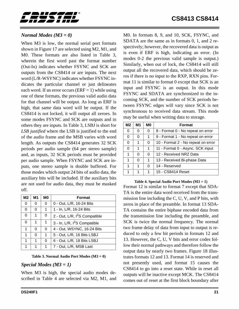
Normal Modes (M3 = 0)
When M3 is low, the normal serial port formatsshown in Figure 17 are selected using M2, M1, andM0. These formats are also listed in Table 3,wherein the first word past the format number(Out-In) indicates whether FSYNC and SCK areoutputs from the CS8414 or are inputs. The nextword (L/R-WSYNC) indicates whether FSYNC in-dicates the particular channel or just delineateseach word. If an error occurs (ERF = 1) while usingone of these formats, the previous valid audio datafor that channel will be output. As long as ERF ishigh, that same data word will be output. If theCS8414 is not locked, it will output all zeroes. Insome modes FSYNC and SCK are outputs and inothers they are inputs. In Table 3, LSBJ is short forLSB justified where the LSB is justified to the endof the audio frame and the MSB varies with wordlength. As outputs the CS8414 generates 32 SCKperiods per audio sample (64 per stereo sample)and, as inputs, 32 SCK periods must be providedper audio sample. When FSYNC and SCK are in-puts, one stereo sample is double buffered. Forthose modes which output 24 bits of audio data, theauxiliary bits will be included. If the auxiliary bitsare not used for audio data, they must be maskedoff.
Table 3. Normal Audio Port Modes (M3 = 0)
Special Modes (M3 = 1)
When M3 is high, the special audio modes de-scribed in Table 4 are selected via M2, M1, and
M0. In formats 8, 9, and 10, SCK, FSYNC, andSDATA are the same as in formats 0, 1, and 2 re-spectively; however, the recovered data is output asis even if ERF is high, indicating an error. (Inmodes 0-2 the previous valid sample is output.)Similarly, when out of lock, the CS8414 will stilloutput all the recovered data, which should be ze-ros if there is no input to the RXP, RXN pins. For-mat 11 is similar to format 0 except that SCK is aninput and FSYNC is an output. In this modeFSYNC and SDATA are synchronized to the in-coming SCK, and the number of SCK periods be-tween FSYNC edges will vary since SCK is notsynchronous to received data stream. This modemay be useful when writing data to storage.
Table 4. Special Audio Port Modes (M3 = 1)Format 12 is similar to format 7 except that SDA-TA is the entire data word received from the trans-mission line including the C, U, V, and P bits, withzeros in place of the preamble. In format 13 SDA-TA contains the entire biphase encoded data fromthe transmission line including the preamble, andSCK is twice the normal frequency. The normaltwo frame delay of data from input to output is re-duced to only a few bit periods in formats 12 and13. However, the C, U, V bits and error codes fol-low their normal pathways and therefore follow theoutput data by nearly two frames. Figure 18 illus-trates formats 12 and 13. Format 14 is reserved andnot presently used, and format 15 causes theCS8414 to go into a reset state. While in reset alloutputs will be inactive except MCK. The CS8414comes out of reset at the first block boundary after
M2 M1 M0 Format
0 0 0 0 - Out, L/R, 16-24 Bits
0 0 1 1 - In, L/R, 16-24 Bits
0 1 0 2 - Out, L/R, I2S Compatible
0 1 1 3 - In, L/R, I2S Compatible
1 0 0 4 - Out, WSYNC, 16-24 Bits
1 0 1 5 - Out, L/R, 16 Bits LSBJ
1 1 0 6 - Out, L/R, 18 Bits LSBJ
1 1 1 7 - Out, L/R, MSB Last
M2 M1 M0 Format
0 0 0 8 - Format 0 - No repeat on error
0 0 1 9 - Format 1 - No repeat on error
0 1 0 10 - Format 2 - No repeat on error
0 1 1 11 - Format 0 - Async. SCK input
1 0 0 12 - Received NRZ Data
1 0 1 13 - Received Bi-phase Data
1 1 0 14 - Reserved
1 1 1 15 - CS8414 Reset
DS240F1 21
CS8413 CS8414
FMTNo. M2 M1 M0
FSYNC (out)
SCK (out)
SDATA (out) LSB MSB LSB MSB
Left Right
MSB
7
FSYNC (out)
SCK (out)
SDATA (out) MSB LSB MSB LSB
LeftRight
LSB
18 Bits18 Bits
6
FSYNC (out)
SCK (out)
SDATA (out) MSB LSB MSB LSB
Left Right
LSB
16 Bits 16 Bits
5
3
FSYNC (in)
SCK (in)
SDATA (out) MSB LSB MSB LSB
Left Right
MSB
FSYNC (out)
SCK (out)
SDATA (out) MSB LSB MSB LSB
Left Right
MSB
2
FSYNC (out)
SCK (out)
SDATA (out) MSB LSB MSB LSB MSB
Left Right4
FSYNC (in)
SCK (in)
SDATA (out) MSB LSB MSB LSB MSB
Left Right1
FSYNC (out)
SCK (out)
SDATA (out) MSB LSB MSB LSB MSB
Left Right
0
11 1
01 1
11 0
10 1
00 1
01 0
10 0
00 0
Figure 17. CS8414 Audio Serial Port Formats
22 DS240F1
CS8413 CS8414
ghe in-r.edhatod-kt-
leaving the reset state. The CS8414 should be resetimmediately after power-up and any time the userperforms a system-wide reset. See Appendix B fora suggested reset circuit.
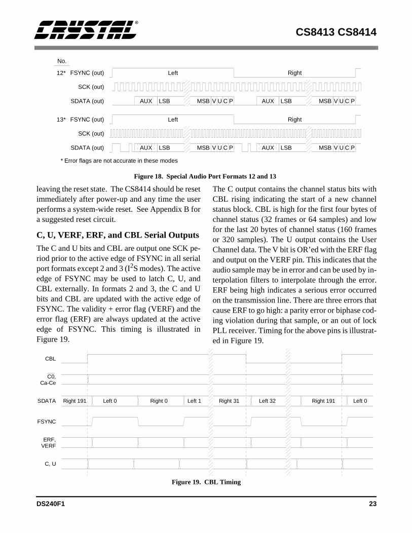
C, U, VERF, ERF, and CBL Serial Outputs
The C and U bits and CBL are output one SCK pe-riod prior to the active edge of FSYNC in all serialport formats except 2 and 3 (I2S modes). The activeedge of FSYNC may be used to latch C, U, andCBL externally. In formats 2 and 3, the C and Ubits and CBL are updated with the active edge ofFSYNC. The validity + error flag (VERF) and theerror flag (ERF) are always updated at the activeedge of FSYNC. This timing is illustrated inFigure 19.
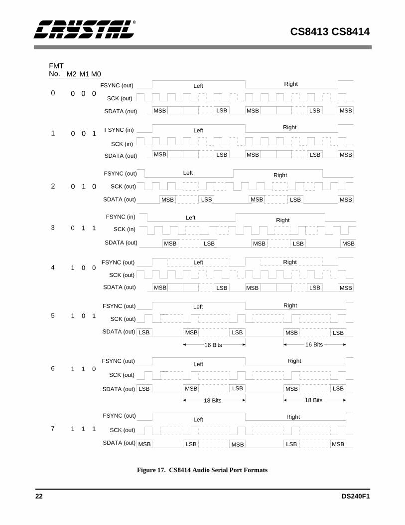
The C output contains the channel status bits withCBL rising indicating the start of a new channelstatus block. CBL is high for the first four bytes ofchannel status (32 frames or 64 samples) and lowfor the last 20 bytes of channel status (160 framesor 320 samples). The U output contains the UserChannel data. The V bit is OR’ed with the ERF flaand output on the VERF pin. This indicates that taudio sample may be in error and can be used byterpolation filters to interpolate through the erroERF being high indicates a serious error occurron the transmission line. There are three errors tcause ERF to go high: a parity error or biphase cing violation during that sample, or an out of locPLL receiver. Timing for the above pins is illustraed in Figure 19.
No.
FSYNC (out)
SDATA (out)
13*
FSYNC (out)
SCK (out)
SDATA (out)
12*
MSB V U C PLSBAUX MSB V U C PLSBAUX
Left Right
Left Right
V U C PLSB V U C PLSB
SCK (out)
MSB MSBAUX AUX
* Error flags are not accurate in these modes
Figure 18. Special Audio Port Formats 12 and 13
CBL
SDATA
FSYNC
Left 0 Left 1Right 0 Left 0Left 32 Right 191Right 31Right 191
C0,Ca-Ce
ERF,VERF
C, U
Figure 19. CBL Timing
DS240F1 23
CS8413 CS8414
r isluetusre-c-vebi-io-he.
on Ta-resp-
aghre.f
on. Ifis-b-nd
Multifunction Pins
There are seven multifunction pins which containeither error and received frequency information, orchannel status information, selectable by SEL.
Error and Frequency Reporting
When SEL is low, error and received frequency in-formation are selected. The error information is en-coded on pins E2, E1, and E0, and is decoded asshown in Table 5. When an error occurs, the corre-sponding error code is latched. Clearing is then ac-complished by bringing SEL high for more thaneight MCK cycles. The errors have a priority asso-ciated with their error code, with validity havingthe lowest priority and no lock having the highestpriority. Since only one code can be displayed, theerror with the highest priority that occurred sincethe last clearing will be selected.
Table 5. Error Decoding
The validity flag indicates that the validity bit for aprevious sample was high since the last clearing ofthe error codes. The slipped sample error can onlyoccur when FSYNC and SCK of the audio serialport are inputs. In this case, if FSYNC is asynchro-nous to the received data rate, periodically a stereosample will be dropped or reread depending onwhether the read rate is slower or faster than the re-ceived data rate. When this occurs, the slipped sam-ple error code will appear on the ‘E’ pins. The CRCerror is updated at the beginning of a channel statusblock, and is only valid when the professional for-
mat of channel status data is received. This erroindicated when the CS8414 calculated CRC vadoes not match the CRC byte of the channel stablock or when a block boundary changes (as in moving samples while editing). The parity error ocurs when the incoming sub-frame does not haeven parity as specified by the standards. The phase coding error indicates a biphase coding vlation occurred. The no lock error indicates that tPLL is not locked onto the incoming data stream
The received frequency information is encoded pins F2, F1, and F0, and is decoded as shown inble 6. The on-chip frequency comparator compathe received clock frequency to an externally suplied 6.144 MHz clock which is input on the FCKpin. The ‘F’ pins are updated three times duringchannel status block including prior to the risinedge of CBL. CBL may be used to externally latcthe ‘F’ pins. The clock on FCK must be valid fotwo thirds of a block for the ‘F’ pins to be accuratThe ‘F’ pins are invalid when the PLL is out olock.
Table 6. Sample Frequency Decoding
Channel Status Reporting
When SEL is high, channel status is displayed C0, and Ca-Ce for the channel selected by CS12CS12 is low, channel status for sub-frame 1 is dplayed, and if CS12 is high, channel status for suframe 2 is displayed. The contents of Ca-Ce depe
E2 E1 E0 Error
0 0 0 No Error
0 0 1 Validity Bit High
0 1 0 Reserved
0 1 1 Slipped Sample
1 0 0 CRC Error (PRO only)
1 0 1 Parity Error
1 1 0 Bi-phase Coding Error
1 1 1 No Lock
F2 F1 F0 Sample Frequency
0 0 0 Out of Range
0 0 1 reserved
0 1 0 reserved
0 1 1 96 kHz ±4%
1 0 0 88.2 kHz ±4%
1 0 1 48 kHz ±4%
1 1 0 44.1 kHz ±4%
1 1 1 32 kHz ±4%
24 DS240F1

CS8413 CS8414
tostter-
at-
rialithe--ebitionpyhehe-
oforype-ute
ingro-
upon the C0 professional/consumer bit. The infor-mation reported is shown in Table 7.
Table 7. Channel Status Pins
Professional Channel Status (C0 = 0)
When C0 is low, the received channel status blockis encoded according to the professional/broadcastformat. The Ca through Ce pins are defined forsome of the more important professional bits. Aslisted in Table 7, Ca is the inverse of channel statusbit 1. Therefore, if the incoming channel status bit1 is 1, Ca, defined as C1, will be 0. C1 indicateswhether audio (C1 = 1) or non-audio (C1 = 0) datais being received. Cb and Cc, defined as EM0 andEM1 respectively, indicate emphasis and are en-coded versions of channel status bits 2, 3, and 4.The decoding is listed in Table 8. Cd, defined asC9, is the inverse of channel status bit 9, whichgives some indication of channel mode. (Bit 9 isalso defined as bit 1 of byte 1.) When Ce, definedas CRCE, is low, the CS8414 calculated CRC valuedoes not match the received CRC value. This signalmay be used to qualify Ca through Cd. If Cathrough Ce are being displayed, Ce going low canindicate not to update the display.
Table 8. Emphasis Encoding
Consumer Channel Status (C0 = 1)
When C0 is high, the received channel status blockis encoded according to the consumer format. Inthis case Ca through Ce are defined differently asshown in Table 7. Ca is the inverse of channel sta-tus bit 1, C1, indicating audio (C1 = 1) or non-audio(C1 = 0). Cb is defined as the inverse of channelstatus bit 2, C2, which indicates copy inhibit/copy-right information. Cc, defined as C3, is the empha-sis bit of channel status, with C3 low indicating thedata has had pre-emphasis added.
The audio standards, in consumer mode, describebit 15, L, as the generation status which indicateswhether the audio data is an original work or a copy(1st generation or higher). The definition of the Lbit is reversed for three category codes: two broad-cast codes, and laser-optical (CD’s). Therefore,interpret the L bit properly, the category code mube decoded. The CS8414 does this decoding innally and provides the ORIG signal that, when low,indicates that the audio data is original over all cegory codes.
SCMS
The consumer audio standards also mention a secopy management system, SCMS, for dealing wcopy protection of copyrighted works. SCMS is dsigned to allow unlimited duplication of the original work, but no duplication of any copies of thoriginal. This system utilizes the channel status 2, Copy, and channel status bit 15, L or generatstatus, along with the category codes. If the Cobit is 0, copyright protection is asserted over tmaterial. Then, the L bit is used to determine if tmaterial is an original or a duplication. (As mentioned in the previous paragraph, the definition the L bit can be reversed based on the categcodes.) There are two category codes that get scial attention: general and A/D converters withoC or L bit information. For these two categories thSCMS standard requires that equipment interfacto these categories set the C bit to 0 (copyright p
Pin Professional Consumer
C0 0 (low) 1 (high)
Ca C1 C1
Cb EM0 C2
Cc EM1 C3
Cd C9 ORIG
Ce CRCE IGCAT
EM1 EM0 C2 C3 C4 Emphasis
0 0 1 1 1 CCITT J.17 emphasis
0 1 1 1 0 50/15 µs emphasis
1 0 1 0 0 No Emphasis
1 1 0 0 0 Not Indicated
DS240F1 25
CS8413 CS8414
tection asserted) and the L bit to 1 (original). Tosupport this feature, Ce, in the consumer mode, isdefined as IGCAT (ignorant category) which is lowfor the “general” (0000000) and “A/D converterwithout copyright information” (01100xx) catego-ries.
26 DS240F1
CS8413 CS8414
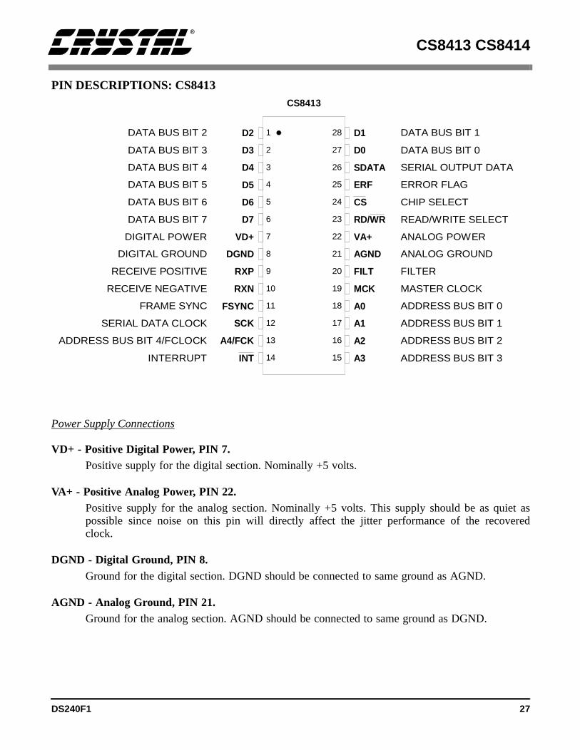
PIN DESCRIPTIONS: CS8413
Power Supply Connections
VD+ - Positive Digital Power, PIN 7.Positive supply for the digital section. Nominally +5 volts.
VA+ - Positive Analog Power, PIN 22.Positive supply for the analog section. Nominally +5 volts. This supply should be as quiet aspossible since noise on this pin will directly affect the jitter performance of the recoveredclock.
DGND - Digital Ground, PIN 8.Ground for the digital section. DGND should be connected to same ground as AGND.
AGND - Analog Ground, PIN 21.Ground for the analog section. AGND should be connected to same ground as DGND.
1
2
3
4
5
6
7
8
9
10
11
12
28
27
26
25
24
23
22
21
20
19
18
17
13
14
16
15
D2 D1DATA BUS BIT 2 DATA BUS BIT 1
D3 D0DATA BUS BIT 3 DATA BUS BIT 0
D4 SDATADATA BUS BIT 4 SERIAL OUTPUT DATA
D5 ERFDATA BUS BIT 5 ERROR FLAG
D6 CSDATA BUS BIT 6 CHIP SELECT
D7 RD/WRDATA BUS BIT 7 READ/WRITE SELECT
VD+ VA+DIGITAL POWER ANALOG POWER
DGND AGNDDIGITAL GROUND ANALOG GROUND
RXP FILTRECEIVE POSITIVE FILTER
RXN MCKRECEIVE NEGATIVE MASTER CLOCK
FSYNC A0FRAME SYNC ADDRESS BUS BIT 0
SCK A1SERIAL DATA CLOCK ADDRESS BUS BIT 1
A4/FCK A2ADDRESS BUS BIT 4/FCLOCK ADDRESS BUS BIT 2
INT A3INTERRUPT ADDRESS BUS BIT 3
CS8413
DS240F1 27
CS8413 CS8414
Audio Output Interface
SCK - Serial Clock, PIN 12.Serial clock for SDATA pin which can be configured (via control register 2) as an input oroutput, and can sample data on the rising or falling edge. As an input, SCK must contain 32clocks for every audio sample in all normal audio serial port formats.
FSYNC - Frame Sync, PIN 11.Delineates the serial data and may indicate the particular channel, left or right. Also, FSYNCmay be configured as an input or output. The format is based on bits in control register 2.
SDATA - Serial Data, PIN 26.Audio data serial output pin.
ERF - Error Flag, PIN 25.Signals that an error has occurred while receiving the audio sample currently being read fromthe serial port. The errors that cause ERF to go high are enumerated in status register 2 andenabled by setting the corresponding bit in IEnable register 2.
A4/FCK - Address Bus Bit 4/Frequency Clock, PIN 13.This pin has a dual function and is controlled by the FCEN bit in control register 1. A4 is theaddress bus pin as defined below. When used as FCK, an internal frequency comparatorcompares a 6.144 MHz clock input on this pin to the received clock frequency and stores thevalue in status register 1 as three FREQ bits. These bits indicate the incoming frequency. Whendefined as FCK, A4 is internally set to 0.
Parallel Interface
CS - Chip Select, PIN 24.This input is active low and allows access to the 32 bytes of internal memory. The address busand RD/WR must be valid while CS is low.
RD/WR - Read/Write, PIN 23.If RD/WR is low when CS goes active (low), the data on the data bus is written to internalmemory. If RD/WR is high when CS goes active, the data in the internal memory is placed onthe data bus.
A4-A0 - Address Bus, PINS 13, 15-18.Parallel port address bus that selects the internal memory location to be read from or written to.Note that A4 is the dual function pin A4/FCK as described above.
D0-D7 - Data Bus, PINS 27-28, 1-6.Parallel port data bus used to check status, read or write control words, or read internal buffermemory.
28 DS240F1

CS8413 CS8414
alog
INT - Interrupt, PIN 14.Open drain output that can signal the state of the internal buffer memory as well as errorinformation. A 5kΩ resistor to VD+ is typically used to support logic gates. All bits affectingINT are maskable to allow total control over the interrupt mechanism.
Receiver Interface
RXP, RXN - Differential Line Receivers, PINS 9, 10.RS422 compatible line receivers. Described in detail in Appendix A.
Phase Locked Loop
MCK - Master Clock, PIN 19.Low jitter clock output of 256 times the received sample frequency.
FILT - Filter, PIN 20.An external 470Ω resistor and 0.068µF capacitor are required from the FILT pin to anground.
DS240F1 29
CS8413 CS8414
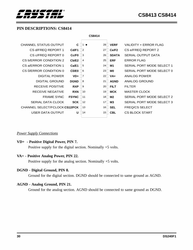
PIN DESCRIPTIONS: CS8414
Power Supply Connections
VD+ - Positive Digital Power, PIN 7.Positive supply for the digital section. Nominally +5 volts.
VA+ - Positive Analog Power, PIN 22.Positive supply for the analog section. Nominally +5 volts.
DGND - Digital Ground, PIN 8.Ground for the digital section. DGND should be connected to same ground as AGND.
AGND - Analog Ground, PIN 21.Ground for the analog section. AGND should be connected to same ground as DGND.
1
2
3
4
5
6
7
8
9
10
11
12
28
27
26
25
24
23
22
21
20
19
18
17
13
14
16
15
C VERFCHANNEL STATUS OUTPUT VALIDITY + ERROR FLAG
Cd/F1 Ce/F2CS d/FREQ REPORT 1 CS e/FREQ REPORT 2
Cc/F0 SDATACS c/FREQ REPORT 0 SERIAL OUTPUT DATA
Cb/E2 ERFCS b/ERROR CONDITION 2 ERROR FLAG
Ca/E1 M1CS a/ERROR CONDITION 1 SERIAL PORT MODE SELECT 1
C0/E0 M0CS 0/ERROR CONDITION 0 SERIAL PORT MODE SELECT 0
VD+ VA+DIGITAL POWER ANALOG POWER
DGND AGNDDIGITAL GROUND ANALOG GROUND
RXP FILTRECEIVE POSITIVE FILTER
RXN MCKRECEIVE NEGATIVE MASTER CLOCK
FSYNC M2FRAME SYNC SERIAL PORT MODE SELECT 2
SCK M3SERIAL DATA CLOCK SERIAL PORT MODE SELECT 3
CS12/FCK SELCHANNEL SELECT/FCLOCK FREQ/CS SELECT
U CBLUSER DATA OUTPUT CS BLOCK START
CS8414
30 DS240F1
CS8413 CS8414
d by
ept in
rnally.
or the
uency
Audio Output Interface
SCK - Serial Clock, PIN 12.Serial clock for SDATA pin which can be configured (via the M0, M1, M2, and M3 pins) asan input or output, and can sample data on the rising or falling edge. As an output, SCK willgenerate 32 clocks for every audio sample. As an input, 32 SCK periods per audio sample mustbe provided in all normal modes.
FSYNC - Frame Sync, PIN 11.Delineates the serial data and may indicate the particular channel, left or right, and may be aninput or output. The format is based on M0, M1, M2, and M3 pins.
SDATA - Serial Data, PIN 26.Audio data serial output pin.
M0, M1, M2, M3 - Serial Port Mode Select, PINS 23, 24, 18, 17.Selects the format of FSYNC and the sample edge of SCK with respect to SDATA. M3 selectsbetween eight normal modes (M3 = 0), and six special modes (M3 = 1).
Control Pins
VERF - Validity + Error Flag, PIN 28.A logical OR’ing of the validity bit from the received data and the error flag. May be useinterpolation filters to interpolate through errors.
U - User Bit, PIN 14.Received user bit serial output port. FSYNC may be used to latch this bit externally. (ExcI2S modes when this pin is updated on the active edge of FSYNC.)
C - Channel Status Output, PIN 1.Received channel status bit serial output port. FSYNC may be used to latch this bit exte(Except in I2S modes when this pin is updated on the active edge of FSYNC.)
CBL - Channel Status Block Start, PIN 15.The channel status block output is high for the first four bytes of channel status and low flast 20 bytes.
SEL - Select, PIN 16.Control pin that selects either channel status information (SEL = 1) or error and freqinformation (SEL = 0) to be displayed on six of the following pins.
DS240F1 31
CS8413 CS8414
status,f
ame 1
eivedMHz.
itizedlearing.
ck on valid. invalid
d fromduring
d.
C0, Ca, Cb, Cc, Cd, Ce - Channel Status Output Bits, PINS 2-6, 27.These pins are dual function with the ‘C’ bits selected when SEL is high. Channel information is displayed for the channel selected by CS12. C0, which is channel status bit 0defines professional (C0 = 0) or consumer (C0 = 1) mode and further controls the definition othe Ca-Ce pins. These pins are updated with the rising edge of CBL.
CS12 - Channel Select, PIN 13.This pin is also dual function and is selected by bringing SEL high. CS12 selects sub-fr(when low) or sub-frame 2 (when high) to be displayed by channel status pins C0 and Cathrough Ce.
FCK - Frequency Clock, PIN 13.Frequency Clock input that is enabled by bringing SEL low. FCK is compared to the recclock frequency with the value displayed on F2 through F0. Nominal input value is 6.144
E0, E1, E2 - Error Condition, PINS 4-6.Encoded error information that is enabled by bringing SEL low. The error codes are priorand latched so that the error code displayed is the highest level of error since the last cof the error pins. Clearing is accomplished by bring SEL high for more than 8 MCK cycles
F0, F1, F2 - Frequency Reporting Bits, PINS 2-3, 27.Encoded sample frequency information that is enabled by bringing SEL low. A proper cloFCK must be input for at least two thirds of a channel status block for these pins to beThey are updated three times per block, starting at the block boundary. These pins arewhen the PLL is out of lock.
ERF - Error Flag, PIN 25.Signals that an error has occurred while receiving the audio sample currently being reathe serial port. Three errors cause ERF to go high: a parity or biphase coding violation the current sample, or an out of lock PLL receiver.
Receiver Interface
RXP, RXN - Differential Line Receivers, PINS 9, 10.RS422 compatible line receivers.
Phase Locked Loop
MCK - Master Clock, PIN 19.Low jitter clock output of 256 times the received sample frequency.
FILT - Filter, PIN 20.An external 470Ω resistor and 0.068µF capacitor is required from FILT pin to analog groun
32 DS240F1
CS8413 CS8414
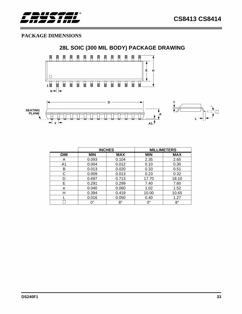
PACKAGE DIMENSIONS
28L SOIC (300 MIL BODY) PACKAGE DRAWING
D
HE
b
A1
A
c
L
∝SEATINGPLANE
1
e
INCHES MILLIMETERSDIM MIN MAX MIN MAX
A 0.093 0.104 2.35 2.65A1 0.004 0.012 0.10 0.30B 0.013 0.020 0.33 0.51C 0.009 0.013 0.23 0.32D 0.697 0.713 17.70 18.10E 0.291 0.299 7.40 7.60e 0.040 0.060 1.02 1.52H 0.394 0.419 10.00 10.65L 0.016 0.050 0.40 1.27∝ 0° 8° 0° 8°
DS240F1 33
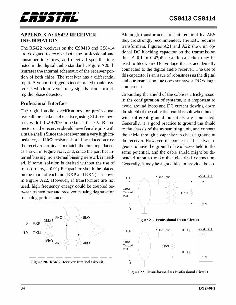
CS8413 CS8414
Sresp-ne
lly ofitalge
e.tonesd.ld
ect atta-
thede-n.p-
APPENDIX A: RS422 RECEIVER INFORMATION
The RS422 receivers on the CS8413 and CS8414are designed to receive both the professional andconsumer interfaces, and meet all specificationslisted in the digital audio standards. Figure A20 il-lustrates the internal schematic of the receiver por-tion of both chips. The receiver has a differentialinput. A Schmitt trigger is incorporated to add hys-teresis which prevents noisy signals from corrupt-ing the phase detector.
Professional Interface
The digital audio specifications for professionaluse call for a balanced receiver, using XLR connec-tors, with 110Ω ±20% impedance. (The XLR con-nector on the receiver should have female pins witha male shell.) Since the receiver has a very high im-pedance, a 110Ω resistor should be placed acrossthe receiver terminals to match the line impedance,as shown in Figure A21, and, since the part has in-ternal biasing, no external biasing network is need-ed. If some isolation is desired without the use oftransformers, a 0.01µF capacitor should be placedon the input of each pin (RXP and RXN) as shownin Figure A22. However, if transformers are notused, high frequency energy could be coupled be-tween transmitter and receiver causing degradationin analog performance.
Although transformers are not required by AEthey are strongly recommended. The EBU requitransformers. Figures A21 and A22 show an otional DC blocking capacitor on the transmissioline. A 0.1 to 0.47µF ceramic capacitor may bused to block any DC voltage that is accidentaconnected to the digital audio receiver. The usethis capacitor is an issue of robustness as the digaudio transmission line does not have a DC voltacomponent.
Grounding the shield of the cable is a tricky issuIn the configuration of systems, it is important avoid ground loops and DC current flowing dowthe shield of the cable that could result when boxwith different ground potentials are connecteGenerally, it is good practice to ground the shieto the chassis of the transmitting unit, and connthe shield through a capacitor to chassis groundthe receiver. However, in some cases it is advangeous to have the ground of two boxes held to same potential, and the cable shield might be pended upon to make that electrical connectioGenerally, it may be a good idea to provide the o
+
-
8kΩ 8kΩ
4kΩ 4kΩ
16kΩ
16kΩ
RXP
RXN
9
10
Figure 20. RS422 Receiver Internal Circuit
XLR
110ΩTwistedPair
* See Text
110Ω
1
RXP
RXN
CS8413/14
Figure 21. Professional Input Circuit
XLR
110ΩTwistedPair
* See Text
110Ω
1
RXP
RXN
CS8413/140.01 µF
0.01 µF
Figure 22. Transformerless Professional Circuit
34 DS240F1
CS8413 CS8414
enic
der
tion of grounding or capacitively coupling toground with a “ground-lift” circuit.
Consumer Interface
In the case of the consumer interface, the standardscall for an unbalanced circuit having a receiver im-pedance of 75Ω ±5%. The connector for the con-sumer interface is an RCA phono plug (fixedsocket described in Table IV of IEC 268-11). Thereceiver circuit for the consumer interface is shownin Figure A23.
TTL/CMOS Levels
The circuit shown in Figure A24 may be used whexternal RS422 receivers or TTL/CMOS logdrive the CS8413/14 receiver section.
Transformers
Please refer Application Note AN134: AES anS/PDIF Recommended Transformers for furthinformation.
RCA Phono
75ΩCoax 75Ω
RXP
RXN
CS8413/140.01 µF
0.01 µF
Figure 23. Consumer Input Circuit
RXP
RXN
CS8413/140.01 µF
0.01 µF
TTL/CMOSGate
Figure 24. TTL/CMOS Interface
DS240F1 35
CS8413 CS8414
APPENDIX B: SUGGESTED RESET CIRCUIT FOR CS8414
The CS8414 should be reset immediately afterpower-up and any time the user issues a system-wide reset. This is accomplished by pulling all four
Mode Select pins high. Figure 25 shows a simplecircuit to implement this. The OR gates can be74LS32 type gates.
CS8414
M0
M1
M2
M3
RESET
M0
M1
M2
M3
Figure 25. CS8414 Reset Circuit
36 DS240F1

• Notes •