Embed Size (px)
Citation preview
Cross-talk analysis in a telecentric adaptive free-spaceoptical relay based on a spatial light modulator
Diego Gil Leyva, Brian Robertson, Charley J. Henderson, Timothy D. Wilkinson,Dominic C. O’Brien, and Grahame Faulkner
We present an analysis of the performance limit of an adaptive multichannel free-space optical inter-connect based on a spatial light modulator (SLM). The SLM function is to provide an active alignment ofthe signal beam in the detector plane. A thorough cross-talk analysis based on the diffractive propertiesof an ideal SLM in an isoplanatic optical system is shown. We analyze the performance in terms of thebit-error rate (BER) due to cross talk between different channels in the optical interconnect for differentalignment states and for different phase-modulation schemes. © 2006 Optical Society of America
OCIS codes: 200.2610, 200.4650, 090.1970, 230.6120.
1. Introduction
Free-space optical interconnects have a wide range ofpotential applications in the fields of telecommunica-tions, computing, and data storage. Of particular in-terest is their use at the printed circuit board–printedcircuit board level to either augment or replace aconventional electronic backplane. This has led to thedemonstration over the past decade of several proto-type systems based on arrays of transceivers and acombination of refractive, diffractive, and polariza-tion optics.1,2 Although it is possible to design a free-space interconnect that is capable of operating atdata rates equal to or greater than conventional elec-tronic backplanes, acceptance of free-space technol-ogy has been slow owing to the perceived difficultiesin aligning a system and in maintaining alignmentduring the operation cycle of a product.3 A directconsequence of these misalignments is an increase inthe bit-error rate (BER) present in the optical inter-connect.4 In this paper we aim to address this funda-mental problem of alignment and to describe howliquid-crystal spatial light modulator (SLM) technol-ogy can be used to produce an adaptive optical relay.
In the context of this paper, an adaptive relay is anoptical system whose alignment state can be exter-nally controlled such that signal throughput is max-imized and interchannel cross talk is minimized.5 Anadaptive relay initially adjusts the alignment state ofthe optics to obtain optimum operation and then con-tinuously adjusts for any drift caused by externalfactors, such as vibrations and thermal cycling,thereby allowing us to minimize the active area of thephotodiodes and reducing the required optical power.This, coupled with the fact that no connectorization isneeded, makes such an approach highly attractive.Adaptive interconnects have been demonstrated byusing a variety of technologies, including Risleyprisms,6 liquid prisms,7 and microelectromechanicalsystems (MEMS).8 In addition, several researchgroups have shown how liquid-crystal SLMs can beused to implement adaptive optical relays.9,10 Theadvantages of using such an approach include thefact that, as there are no moving parts, the long-termreliability will be better than that in a mechanical-based system. In addition, the deflection angle is afunction of hologram pattern only, and thus the beamis deflected to exactly the same point for the samepattern at any given time. The discrete nature of anSLM and the fact that it operates in the Fourier planemake it relatively insensitive to pixel errors, therebyoffering the possibility of a high-yield fabrication pro-cess. Moreover, it is possible to correct for aberrationsin the optical system that are introduced by fabrica-tion or alignment errors—a key advantage in high-performance optical relays. Finally, in the case of aliquid-crystal-on-silicon (LCOS) device,10 in whichthe pixels are deposited on a silicon substrate by
D. Gil Leyva ([email protected]), B. Robertson, C. J. Henderson,and T. D. Wilkinson are with the Engineering Department, Pho-tonics and Sensors Group, Cambridge University, TrumpingtonStreet, Cambridge CB2 1PZ, UK. D. C. O’Brien and G. Faulknerare with the Department of Engineering Science, University ofOxford, Parks Road, Oxford OX1 3PJ, UK.
Received 30 March 2005; revised 31 August 2005; accepted 2September 2005.
0003-6935/06/010063-13$15.00/0© 2006 Optical Society of America
1 January 2006 � Vol. 45, No. 1 � APPLIED OPTICS 63
using standard complementary metal-oxide semicon-ductor (CMOS) processing, we can, in principle, com-bine the control electronics with the SLM to producea faster, more compact device. The obvious drawbackwith SLMs relates to the propagation of higher dif-fraction orders through the system. It can be shownthat any quantized hologram structure generateshigher diffraction orders, with the relative power ineach order being determined by the exact profile ofthe phase pattern and by the incident-beam profile.Thus, in the case of a multichannel optical intercon-nect, these noise orders can, in certain alignmentstates, land on the detector of a neighboring channeland reduce the optical performance of the link. Mul-tilevel phase SLMs have the obvious advantage ofincreasing the power diffracted into the signal beamorder and suppressing the higher orders. However, inthe context of an adaptive optical interconnect, fer-roelectric SLMs, which can only modulate light in abinary fashion, yield a higher frame rate.
In this paper we address this cross-talk problemand explore the capabilities and limitations of anoptical interconnect with an adaptive alignment ap-proach that provides the coverage required for aboard-to-board interconnect. Although a binaryphase configuration is the least efficient, it is advan-tageous from the point of view of reducing SLM costand control complexity.
The trade-off among the relay geometry, the num-ber of phase levels, and the cross-talk performance isinvestigated with the aim of determining the opti-mum arrangement capable of implementing an align-ment tolerant board-to-board relay. In addition, weconsider a board-to-board interconnect compatiblewith a 1 � A fiber-ribbon interconnect,11 where A is
the number of channels, because these componentsare already available commercially and set a chal-lenging target to aim for. It should be stressed thatthe advantage of a free-space relay is its scalability tolarge two-dimensional arrays of communicationlinks, thereby permitting either higher data-transferrates or lower communication speeds for each chan-nel for the same overall data-transfer rate. It is ourintention to generalize this model for two-dimensional arrays in a later publication.
The outline of the paper is as follows. In Section 2we outline the layout of an adaptive optical relay. InSection 3 we discuss some of the fundamental limitsassociated with using a pixelated phase hologram inan adaptive relay. Section 4 presents a BER modelthat is used to assess the optical performance of anadaptive optical interconnect in the presence ofhigher diffraction orders. We then discuss the prob-lems associated with using a simple one-to-onesymmetric vertical-cavity surface-emitting laser (VC-SEL) to detector geometry and calculate the mini-mum number of phase levels required to implementsuch a system (Section 5). Throughout this paper weattempt to outline the practical engineering problemsinvolved in realizing such a system.
2. Outline of the System
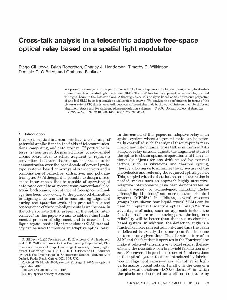
An example of an adaptive board-to-board relaybased on a LCOS SLM is shown in Fig. 1. The linkconsists of an array of VCSELs and a matching arrayof photodiodes interconnected by a telecentric relay.To maximize the optical performance of the system,we used a SLM to steer the signal beams onto theactive area of the photodiodes, which we shall refer toas the detector window. Electrical data are sent to the
Fig. 1. Reflective adaptive interconnect based on a reconfigurable LCOS SLM.
64 APPLIED OPTICS � Vol. 45, No. 1 � 1 January 2006
VCSEL array and are converted into an optical datastream. It is assumed that the VCSELs emit a lin-early polarized beam of light, which is collimated bythe first lens. The light passes through the polarizingbeam splitter (PBS) and is changed into circularlypolarized light by the quarter-wave plate (QWP). Af-ter being reflected from the LCOS SLM, the signalbeams again pass through the QWP, where the po-larization state is converted into linearly polarizedlight orthogonal to the polarization state of the inputbeam. As a result, the signal beams are reflected bythe PBS and then focused down onto the photodiodearray, where the data are then transferred to theelectronics on the second printed circuit board. Itshould be noted that such a system is capable ofsupporting a bidirectional data link. That is, the op-toelectronic device arrays on PCB1 and PCB2 cancontain both emitters and detectors. An additionalpoint that must be covered relates to the speed ofadaptation. When the board is initially inserted intothe chassis, the adaptive relay must perform a scan todetermine the misalignment and to display the opti-mum hologram that maximizes the power coupledinto the photodetectors. The packaging of this systemis critical in determining the alignment tolerances ofthe optical relay. Throughout this analysis it is as-sumed that the VCSEL collimating lens is prealignedto the transmitter PCB and that the detector–focusing lens is prealigned with respect to the re-ceiver board, as shown in Fig. 1. Thus an error in the
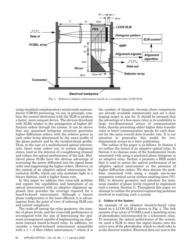
board separation of �z will have a negligible effect onrelay performance, and as long as the aberrationsintroduced by a ��x, �y� misalignment are such thatthe system is either insensitive to the error or, per-haps more important, the LCOS SLM can correct forthe aberrations by optimizing the hologram pat-tern.12,13 We are therefore left with tilt errors ��, ��that can be corrected for by changing the hologrampattern displayed on the hologram (see Fig. 2) andthe rotation errors, �, about the z axis.
This study concentrates on an adaptive relay thatis compatible with a standard 1 � 12 fiber-ribbonrelay. Throughout this analysis we assume that weare designing a free-space interconnect with a board-to-board spacing, dPCB, of 30 mm. However, in prac-tice the spacing can be set at any value by correctdesign of the interconnect. A standard VCSEL pitchis dp � 250 �m. The operating wavelength is �� 850 nm. A standard value for the photodetectordimensions, dw, is 15 �m. Useable values for the re-lay focal length of the configuration shown in Fig. 1were calculated to be approximately 13 mm. For op-timum operation, the SLM must be positioned at thefocal plane of lens L1, ensuring that the system istelecentric and therefore less sensitive to misalign-ments.14 If necessary, an optical spacer can be intro-duced in the interconnect to attain the conditions fora 4F system. The ideal SLM used for modeling theinterconnect has N � 128 pixels along each dimen-sion with a pixel pitch � equal to 15 �m. We assume
Fig. 2. Transmissive SLM architecture for a 4 � 4 adaptive optical interconnect for (a) a perfectly aligned system and (b) a system inwhich a tilt error of � is present.
1 January 2006 � Vol. 45, No. 1 � APPLIED OPTICS 65
that the SLM can perform binary, quaternary, oroctonary phase modulation on the incoming light.Increasing the number of phase levels, even in thecase of having a continuous-phase modulation, willnot increase the diffraction efficiency significantlyabove that of a system utilizing an eight-phase-leveldevice.
3. Limits Associated with a Pixelated Hologram
The effects of using a pixelated device for beam steer-ing, such as the spreading of higher orders, aliasing,and sinc envelope, are well known.15,16 In the case ofan adaptive relay it is necessary to have a completemodel so that we can compute the relative intensitydistribution of the replay field as a whole, particu-larly when more than one channel is transmittedthrough the system.
A. Hologram Limitations
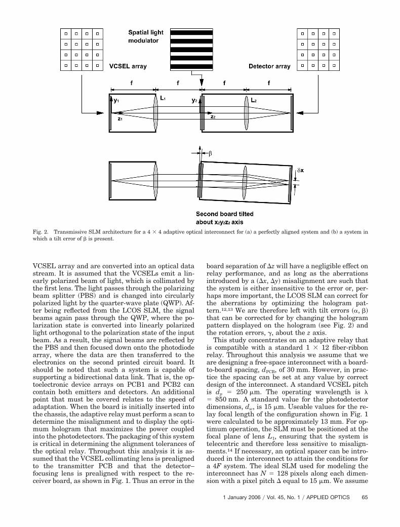
To investigate the limits associated with a telecentricadaptive relay, let us first look at the simplest kind ofinterconnect in which the VCSELs are arranged on aregular grid and each VCSEL has a single corre-sponding detector, as shown in Fig. 3. The effect of tilterror, ��, ��, will result in a shift of the zeroth orderby a distance �d�, d�. In the paraxial regime
d� � F(tan �),
d � F(tan �), (1)
where F is the focal length of the lenses. In this casewe can perform beam steering with a diffractive el-ement that allows us to tilt the wave front. In thisway the ideal transmittance of the beam-steeringhologram in the paraxial regime should be
h(x) � exp�ik�(xd�) (yd)�
F �. (2)
In practice an M phase-level SLM consists of an N� N array of pixels, each of dimension � � �. Thisintroduces limitations in terms of both diffractionefficiency and positioning accuracy, which vary as afunction of tilt angle. In Subsection 3.C we discussthese limitations and their implications in terms ofsystem design. The physical coordinates pair �d�, d�,representing the misalignment, is related to thespatial-frequency coordinates pair �dfX, dfY� as17
dfX �d�
�F, dfY �d
�F. (3)
In this way we say that the input and output planesare related by a Fourier transform. Since we are us-ing a pixelated element to steer the beam, we can alsorelate the coordinate pair representing the misalign-ment to the characteristics of the SLM device. Thisnew transformation is18
du � d�
N�
�F , dv � d
N�
�F . (4)
The quantity du has a close relation with the spatial-frequency term dfX, but it is not the same. The termdu�N referred to as a spatial frequency in cycles persampling interval.19 The quantities du, dv are definedin the plane given by coordinates �u, v�.
B. Hologram Algorithm
To perform beam steering with a diffractive element,we adapt a modulo 2� algorithm20 whereby we first
Fig. 3. Illustration of VCSEL-array and detector-array layouts in a 1 � A relay in which there is a one-to-one correspondence betweenVCSELs and detector windows. Beam steering occurs when the correct hologram pattern is displayed.
66 APPLIED OPTICS � Vol. 45, No. 1 � 1 January 2006
calculate the linear phase shift required to direct the1 order into the detector window position. Thislinear-phase ramp is given by the argument of Eq.(2):
�(xh, yh) �2�(xhdu yhdv)
N . (5)
The subscript h in coordinates �xh, yh� means thatthey represent pixels instead of physical positions. Toinclude the phase quantization, we use a nonlinearoperand to hardclip the phase function according tothe number of available discrete phases. The aboveprocedure includes both the phase and the spatialquantization restrictions. Owing to the aforemen-tioned one-to-one correspondence, this hologram gen-eration will be sufficient.
C. Variation of Diffraction Efficiency with Tilt Angle
By implementing the nonlinear procedure describedin Subsection 3.B, we make our system dispersive.That is, optical power will be diffracted into noiseorders. Moreover, due to space quantization, therewill exist multiple replications of the diffraction or-ders at the far field (output plane).15 Also, the powerof the signal beam will decrease as we move fartheraway from the optical axis. To gain more insight intothe effect that this procedure will have in the far field,we perform a step-by-step analysis of the phase andspace quantization procedures involved. In the caseof dealing with binary phase holograms, binarizingan ideal transmission function as the one shown inEq. (2) can be accomplished by taking the value of theoutput to be the sign of the original transmittancefunction. This output binary transmission function inthe one-dimensional (1D) case, hb, can be representedas a Fourier series expansion21:
hb(x) � 2 �n*� �
� sin��(n�2)��n exp(2�ixndfX), (6)
where the superscript * denotes that n cannot take azero value. We can see that the Fourier plane will becharacterized by a series of delta functions spacedn � dfX from each other and with associate intensitygiven by sinc�n�2�2. Clearly, the signal beam will bethe first diffraction order and will be located at theposition fX � dfX. Moreover, by looking at Eq. (6) wecan see that the intensity of each diffraction order isgiven by Dammann’s expression22 for a two-phase-level grating. We can generalize Eq. (6) for an Mphase-level grating as
hm(x) � �g� �
� sin��(n�m)��n�m exp(2�ixndfx), (7)
where the diffraction orders are given by n � gM 1.
To add the effect of space quantization, first we needto add the effect of the limited size of the SLM. This canbe accomplished by multiplying the transmission func-tion with an aperture function of the size specified bya rect function.17 Then we need to sample the result ata rate equal to the pixel pitch �. The sampling proce-dure can be accomplished by multiplying the resultwith a train of delta functions centered at the origin.Finally, we need only to convolve the result with anaperture function that describes the clear aperture ofeach pixel. The size of this aperture is smaller than thepixel pitch because there is typically some dead spacebetween pixels. Thus the ratio between the clear ap-erture of a pixel and the pixel pitch will be representedby �. Putting all this into an expression and in thecorrect order of physical correspondence, we have atransmission function t�x� given by
t(x) � rect x����combx
��rect xN�h(x)��, (8)
where the comb function is the sampling function.17
To gain more control of Eq. (8), we can include a termthat offsets the sampling function away from the or-igin when required. This is necessary when we sam-ple certain distributions in which the transition point(from 1 to 1 in the binary case) lands exactly on aposition that is a multiple of the sampling rate �. Inthis way an alternate transmission function would be
t(x) � rect x������(x s) � combx
��� �rect x
N�h(x)��, (9)
where s can be any value from 0 to � but in most caseswill be set to zero. To know the normalized intensitydistribution at the output plane, we set � � 1. AfterFourier transforming Eq. (9), we have at the outputplane
T(fX) � �� sinc(��fX) �exp(i2�fXs)� comb(�fX)�� N� sinc(N�fX) � H(fX)�, (10)
where H�fX� is the Fourier transform of h�x� in Eq. (7).After reducing the convolution terms and normaliz-ing the sinc function, we get
T(fX) � � sinc(��fX)�exp(i2�fXs)sin(N��fX)N sin(��fX)
� cos(��fX)�� H(fX), (11)
where we have made use of the residue theorem23 tosimplify the expression. Thus, by substituting theseries expansion for H�fX� in Eq. (11), we obtain
1 January 2006 � Vol. 45, No. 1 � APPLIED OPTICS 67
T(fX) � � sinc(��fX)�exp(i2�fXs)sin(N��fX)N sin(��fX)
� cos(��fX)�� �g� �
�
sinc nM�(fX dfX), (12)
and after performing the convolution we get
T(fX) � � sinc(��fX)( �g� �
�
sinc nM�exp[i2�(fX ndfX) s]
�sin�N��(fX ndfX)�N sin���(fX ndfX)�
cos[��(fX ndfX)]�),
(13)
where again n � gM 1. Hence the intensity distri-bution is given by |T�fX�|2. From Eq. (13) we can seethe effect of the sinc envelope in the diffraction effi-ciency as we change the position of the first diffrac-tion order (deflection angle). The fourth term fromleft to right in the last expression, the Dirichlet func-tion or periodic sinc function, shows us the effect ofthe number of pixels in the replay field. With a smallnumber of pixels, the sidelobes of each nonzero peakin the replay field will be more accentuated. If weincrease the number of pixels, the number of side-lobes will increase; however, their intensity will de-crease. In this way, by examining the zeros of thesecond sinc function in Eq. (10), we can see that thewidth of the peaks in the replay field will be given by2�N� spatial frequencies. In other words, the widthwill be given by 2�F�N� in terms of spatial units. Foran SLM having N � 128 pixels and a feature size of� � 30 �m and using an imaging lens with focallength F � 13.5 mm, we will have a spot width ofapproximately 10 �m at � � 850 nm. Therefore, hav-ing a photodetector size of 15 �m as mentioned beforeshould be adequate for such a system. Nonetheless,we need to take into account that the SLM illumina-tion is not uniform but has a Gaussian distribution.This will result in a further broadening in the spot’swidth and a decrease of its peak intensity, dependingon the beam characteristics such as the beam waist�o. If the beam waist �o is much bigger than the spotsize given by 2�F�N�, then Eq. (13) will not give anaccurate description of the replay field. The effect ofGaussian apodization can be calculated numericallyas
Tg(fX) � T(fX) � G(fX), (14)
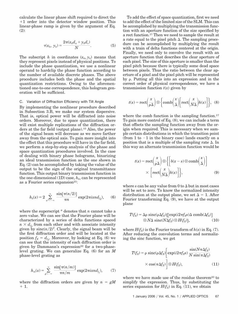
where G�fX� is the Gaussian distribution at the outputplane. It is important to note that, since we are deal-ing with a coherent source, we have to convolve theamplitudes before calculating the final intensity.Having a beam waist wo � 5 �m will result in aminimum result variation from using Eq. (14) or (13).Figures 4(a), 4(b), and 4(c) show the superimposedplots of the intensity distribution as we scan the re-
play field (i.e., the detector plane), using an SLM withN � 128 pixels and 2, 4, and 8 phase levels, respec-
Fig. 4. Superimposed plots arising from the scanning of the re-play field by changing the position of the first diffraction order fromdu � 0 to du � N�2, using an SLM with N � 128 pixels, � � 0.8, andphase levels of (a) 2, (b) 4, and (c) 8. In the plot we can see theroll-off of the intensity due to the sinc envelope. Moreover, thereare certain peaks along the curve that are due to multiple repli-cation orders landing at the same position.
68 APPLIED OPTICS � Vol. 45, No. 1 � 1 January 2006
tively. As we change the position of the first order wecan see how the sinc envelope diminishes the inten-sity until it reaches its minimum. We can see that dueto the multiple replication orders (aliasing) there aresome positions where the intensity from other higherorders overlaps at the same position. Moreover, wecan see that when no grating is displayed, the max-imum peak is located at the origin and in that case|T�dfx�|2, which we can infer from a simple inspectionof Eq. (13). This is in agreement with the model de-scribed in Ref. 16 in which a fill factor � that issmaller than unity is considered. In the absence ofdead space, all the light intensity passing through theideal-phase hologram plane should end at the outputplane. Nevertheless, there is a fraction of energy ab-sorbed in the hologram plane owing to dead space. Tovisualize this better, we can approximate the twoterms on the right-hand side of Eq. (13) as the sum ofdelta functions spaced 1�� from each other. This ap-proximation is valid when the extent of the device isbig enough and no appreciable broadening of thespots due to diffraction can be seen. In this case thenew relation will be
T(fX) � � sinc(��fX)� �q� �
�
��fX q�
dfX��.
(15)
The fraction of light absorbed owing to dead space isrelated to the fill factor � as 1 � since it can beproved, starting now from Eq. (15), that24
�q� �
�
�2 sinc2���q�
dfX�� �, (16)
regardless of the value of the positioning dfX. Equa-tion (16) represents an integration of the power end-ing in the output plane.
Up to this stage we have dealt with on-axis sources.In an isoplanatic17 optical system the calculation ofthe field for an off-axis source consists of an extraconvolution applied to Eq. (13) as follows:
T�(fX) � T(fX) � �(fX �), (17)
T�(fX) � � sinc[��(fX �)]� �g� �
�
sinc nM
�sin�N��(fX ndfX �)�N sin���(fX ndfX �)�
� cos[��fX ndfX �)]�. (18)
We note that the sinc envelope now is centeredaround the value of �, which refers to the position ofthe zeroth order in the spatial-frequency plane.
D. Spatial Light Modulator Choice
The choice of liquid-crystal SLM technology is essen-tially a trade-off between the number of phase levels
that can be produced at each pixel and the minimumframe rate that can be displayed. Nematic devicescan achieve multilevel phase modulation, but theyhave relatively slow switching speeds when com-pared with ferroelectric devices. Ferroelectrics, how-ever, are currently capable only of binary phasemodulation and require dc balancing; that is, eachpixel is held in positive and negative states for equalamounts of time. One technique capable of providingdc balancing is scrolling,20 in which the hologrampattern is shifted one pixel or column at a time. Anincrease in the number of phase levels will result inimprovements to both the diffraction efficiency andthe cross talk present in the optical system, as dis-cussed further in Section 5 of this paper. This willultimately affect the achievable BER of the opticallink. The need for a minimum frame rate comes fromthe maximum frequency of vibration that the adap-tive link is expected to tolerate.25 When the SLM isconsidered as part of a discrete time–position controlloop, its switching time limits the controller samplerate. A simpler kind of correction is required owing toa gradual drift in the alignment state of the systemdue to the long-term effects of internal and externalvibrations and to thermal cycling.26 Rack-mountedequipment in static locations may be expected to tol-erate vibrations of up to �100 Hz—increasing formore demanding environments, such as aircraft, inwhich it can go up to 1 Khz.27 To reject harmonicdisturbances up to a given frequency, the controllersample rate needs to be approximately ten timesgreater than this frequency. At the present time, fer-roelectric devices are the only ones capable of achiev-ing frame rates in excess of 1 kHz. However,developments in nematic liquid-crystal technologymake it likely that these rates may soon become fastenough to approach the speeds necessary for less de-manding environments. To this end, the optical per-formance of the system for varying numbers of phaselevels is considered in this paper, allowing us to in-vestigate the potential performance of both nematicand ferroelectric SLM technology.
E. Limitations Associated with Grating Period
Another practical limitation of the performance of thegratings is the minimum achievable deflection angle.A large grating period is required for small deflec-tions. Although, the plots in Fig. 4 show no restrictionwith respect to applying a grating period that is smallenough so that the signal beam is closer to the zerothorder, in reality there is a limit as to where the num-ber of periods displayed in the SLM will not be suf-ficient. Thus the resulting diffraction orders will notbe cleanly formed, and the power and position of the1 and 1 orders will vary as the positioning of thegrating in space is altered. This performance limithas been verified experimentally by scrolling gratingsof increasing period on an SLM to find the point atwhich the diffraction pattern ceases to be invariantwith respect to different scrolling positions. The ex-perimental system is equivalent to the system de-picted in Fig. 2. Light from a laser diode operating at
1 January 2006 � Vol. 45, No. 1 � APPLIED OPTICS 69
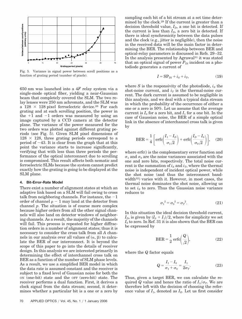
650 nm was launched into a 4F relay system via asingle-mode optical fiber, yielding a near-Gaussianbeam that completely covered the SLM. The two re-lay lenses were 250 nm achromats, and the SLM wasa 128 � 128 pixel ferroelectric device.28 For eachgrating and at each scrolling position, the power inthe 1 and 1 orders was measured by using animage captured by a CCD camera at the detectorplane. The variance of the power measured for thetwo orders was plotted against different grating pe-riods (see Fig. 5). Given SLM pixel dimensions of128 � 128, three grating periods correspond to aperiod of �43. It is clear from the graph that at thispoint the variance starts to increase significantly,verifying that with less than three periods the per-formance of the optical interconnect due to scrollingis compromised. This result affects both nematic andferroelectric SLMs because the system cannot predictexactly how the grating is going to be displayed at theSLM plane.
4. Bit-Error-Rate Model
There exist a number of alignment states at which anadaptive link based on a SLM will fail owing to crosstalk from neighboring channels. For instance, the 1order of channel � 1 may land at the detector fromchannel p. The situation is of course more complexbecause higher orders from all the other signal chan-nels will also land on detector windows of neighbor-ing channels. As a result, the majority of the channelswill fail. This process is repeated for higher diffrac-tion orders in a number of alignment states; thus it isnecessary to consider the cross talk from all A chan-nels in our analysis over all values of ��, �� to calcu-late the BER of our interconnect. It is beyond thescope of this paper to go into the details of receiverdesign. In this analysis we are interested primarily indetermining the effect of interchannel cross talk onBER as a function of the number of SLM phase levels.As a result, we use a simplified BER model in whichthe data rate is assumed constant and the receiver issubject to a fixed level of Gaussian noise for both theON (one-bit) state and the OFF (zero-bit) state. Thereceiver performs a dual function. First, it derives aclock signal from the data stream; second, it deter-mines whether a particular bit is a one or a zero by
sampling each bit of a bit stream at a set time deter-mined by the clock.29 If the current is greater than adecision threshold value, ID, a one bit is detected. Ifthe current is less than ID, a zero bit is detected. Ifthere is ideal synchronicity between the data pulsesand the clock (e.g., jitter is negligible), then the noisein the received data will be the main factor in deter-mining the BER. The relationship between BER andoptical-relay parameters is discussed in Refs. 29–32.In the analysis presented by Agrawal31 it was statedthat an optical signal of power PIN incident on a pho-todiode generates a current of
I � SPIN iS iT, (19)
where S is the responsivity of the photodiode, iS theshot-noise current, and iT is the thermal-noise cur-rent. The dark current is assumed to be negligible inthis analysis, and we deal with a typical data streamin which the probability of the occurrence of either aone or a zero is 50%. Let us assume that the averagecurrent is I0 for a zero bit, and I1 for a one bit. In thecase of Gaussian noise, the BER of a simple opticallink in the absence of interchannel cross talk is givenby
BER �14 �erfcI1 ID
�1�2 erfcID I0
�0�2 �, (20)
where erfc�� is the complementary error function and�1 and �0 are the noise variances associated with theone and zero bits, respectively. The total noise cur-rent is the summation of iS and iT, where the thermalnoise is independent of incident optical power, whilethe shot noise (and thus the interconnect band-width32) varies with it. However, in most cases, thethermal noise dominates the shot noise, allowing usto set iS to zero. Thus the Gaussian noise variancereduces to
�12 � �0
2 � �T2. (21)
In this situation the ideal decision threshold current,ID, is given by �I0 I1��2, where for simplicity we setI0 to zero. In Ref. 31 it is also shown that the BER canbe expressed by
BER �12 erfcQ
�2, (22)
where the Q factor equals
Q �I1 I0
�1 �0�
I1
2�T. (23)
Thus, given a target BER, we can calculate the re-quired Q value and hence the ratio of I1��T. We aretherefore left with the decision of choosing the refer-ence value of I1, denoted as IR. Let us first consider
Fig. 5. Variance in signal power between scroll positions as afunction of grating period (number of pixels).
70 APPLIED OPTICS � Vol. 45, No. 1 � 1 January 2006
the BER performance of a binary-phase optical linkin the absence of interchannel optical cross talk. Inthis analysis we restrict ourselves to the case of alinear 1 � A data link. Let us assume that the tilterror about the x axis is zero and that we are dealingonly with a tilt angle � (see Fig. 2). This is of coursea worst-case scenario because, due to the symmetry ofthe system, the higher diffraction orders will lie alonga line bisecting the detector windows of the receiverarray (see Fig. 3); thus a 1 � A system will be moresensitive to multichannel cross talk. As mentioned inSubsection 3.C, the diffraction efficiency of the beam-steering grating varies as a function of � (Fig. 4).Then I1 � S���, M�PIN, where M is the number ofphase levels. Also, we need to take into account thefinite extent Ad of the photodetector device as
�(�, M) ���Ad
|T�g(fX, fY)|2dfXdfY. (24)
To know the amount of tilt correction that we canperform in the optical system, let us consider Figs.4(a)–4(c). Starting from a fixed-bias period gratingthat directs the signal beam (first diffraction order) tothe N�4 position in the u plane, we can see that themaximum range is the one indicated by the arrows inthe plots shown in Fig. 4. This range of availablecorrection comes from the fact that we cannot placethe first diffraction order farther than the maximumposition specified by the SLM structure, which is du
� N�2. Although we can see some light sweepingbeyond this limit, it is due to higher orders ratherthan to the signal beam. The opposite limit is speci-fied in the discussion in Subsection 3.E, in which weconcluded that working very close to the central re-gion would cause power stability problems. Then,starting at a bias position du � N�4, we can correctwithin a range of � N�4, N�4�. For the purposes ofthis analysis, we choose the reference point for ourcalculation to occur at the position du � N�2 1 inthe first-order scanning of the replay field and for thecase of using a binary SLM [Fig. 4(a)]. The reason forchoosing this value of du to obtain IR is only becauseit has the lowest intensity in the plots shown in Fig.4, which is obviously within the aforementionedsteering range. From Eq. (13) it can be shown that thediffraction efficiency at this position is 15% of thetotal energy.
Thus, assuming a responsivity of S � 0.5 and anincident power of PIN � 1 mW, the correspondingvalue of IR � 75 �A. In this paper we set a targetoperational BER of 10 12. As cross talk will degradethis value, we set the BER for a cross-talk free link at10 13, resulting in a Q value of 7.35 and a Gaussiannoise variance of �T � 3.7 �A. Throughout the rest ofthis analysis, we keep these values of �T and PIN fixed.The value of I1, and thus those of Q and BER, willvary as we calculate the optimum hologram patternto deflect the signal to the detector window and as weincrease the number of phase levels.
In the case of a relay in which there are A datachannels, the situation is obviously far more complex.If data are sent on channel p, we must consider theeffect of cross talk from the remaining A 1 chan-nels. Let us consider cross talk from channel q, wherethe cross-talk power into our signal channel p is givenby cq. This represents the percentage of the signalpower from VCSEL q that is coupled into signal chan-nel p from all the diffraction orders generated byVCSEL q. Note that the cross-talk power is taken tobe constant (no Gaussian noise considered). We rep-resent the state of channel q as bq, where bq � 1 whenchannel q is in the ON state and bq � 0 when channelq is in the OFF state. In general the probability of a oneor a zero equals 0.5. Thus the BER of channel p isgiven by
BER(p) �1
2A 1 �b1�0
b1�1
�b2�0
b2�1
· · · �bA�0
bA�1
�14 �erfcID Ioffset I0 Ixt
�T�2 erfcI1 Ixt ID Ioffset
�T�2 � (25)
for all values of bq with the exception of q � p (signalchannel does not introduce a cross-talk term). Weadded an offset term, Ioffset, to account for the fact thatthe relay in general operates in the presence of abackground noise level. Thus the decision level, ID,can be raised to ID Ioffset to improve performance.The value of Ioffset is given by the maximum currentinduced by all the other signal channels divided bytwo:
Ioffset �12 �
q�1, q�p
A
Scq. (26)
This is a measurable term because during operationof the system we can switch on all the adjacent signalchannels and measure its value. The term Ixt is re-lated to the cross-talk values by
Ixt � �q�1, q�p
A
S(bqcq). (27)
In both Eqs. (26) and (27) the value of cq, the powercoupled into the detector window of channel p fromchannel q, is calculated by integration of the intensityaccording to the two-dimensional version of Eqs. (13),(14), and (18) over the area of the photodetector foreach adjacent channel at the detector in the windowof interest.
5. Simple Telecentric Adaptive Board-to-Board RelayInterconnect
In this section we calculate the effective cross talkthat reaches channel p as a function of alignment ina linear 1 � 12 channel relay, as well as the corre-sponding BER of the central channel of the relay as a
1 January 2006 � Vol. 45, No. 1 � APPLIED OPTICS 71
function of the angular misalignment and the num-ber of phase levels. The adaptive interconnect param-eters are the same as those derived in Section 2.
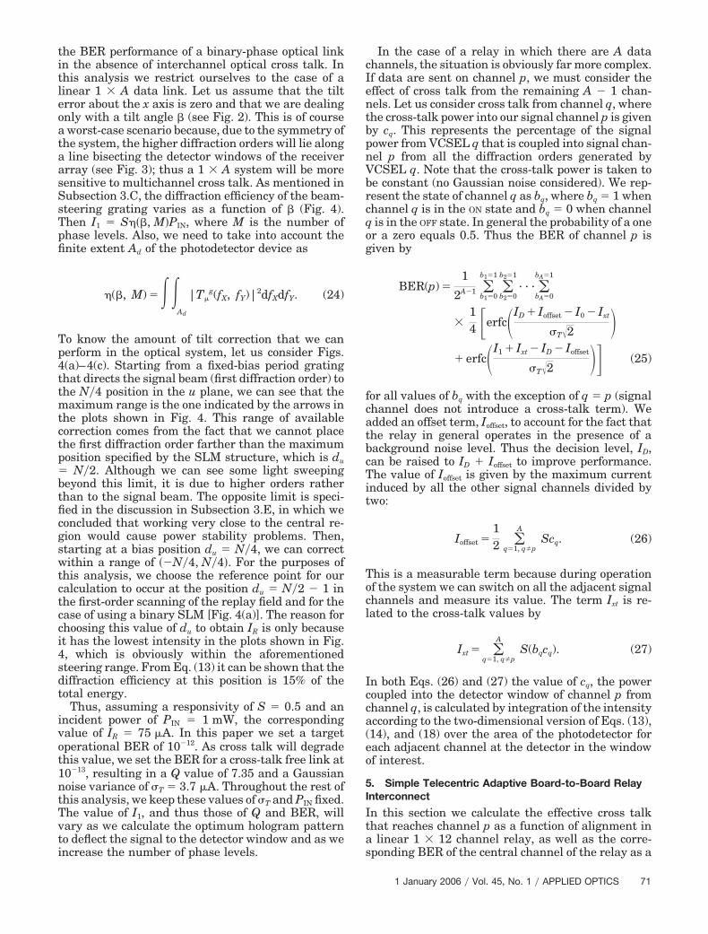
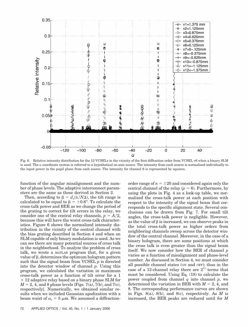
Then, according to � � du���N��, the tilt range iscalculated to be equal to � � �0.6°. To calculate thecross-talk power and BER as we change the period ofthe grating to correct for tilt errors in the relay, weconsider one of the central relay channels, p � A�2,because this will have the worst cross-talk character-istics. Figure 6 shows the normalized intensity dis-tribution in the vicinity of the central channel withthe bias grating described in Section 4 and when anSLM capable of only binary modulation is used. As wecan see there are many potential sources of cross talkin the neighborhood. To analyze the problem of crosstalk, we wrote a MATLAB program that, for a givenvalue of �, determines the optimum hologram patternsuch that the signal beam from VCSEL p is directedinto the detector window of channel p. Using thisprogram, we calculated the variation in maximumcross-talk power as a function of tilt error for a 1� 12 adaptive relay based on a binary phase SLM forM � 2, 4, and 8 phase levels [Figs. 7(a), 7(b), and 7(c),respectively]. Numerically, we obtained similar re-sults when we included Gaussian apodization with abeam waist of �o � 5 �m. We assumed a diffraction-
order range of n � �20 and considered again only thecentral channel of the relay �p � 6�. Furthermore, byusing the plots in Fig. 4 as a look-up table, we nor-malized the cross-talk power at each position withrespect to the intensity of the signal beam that cor-responds to the specific alignment state. Several con-clusions can be drawn from Fig. 7. For small tiltangles, the cross-talk power is negligible. However,as the value of � is increased, we can observe peaks inthe total cross-talk power as higher orders fromneighboring channels sweep across the detector win-dow of the central channel. Moreover, in the case of abinary hologram, there are some positions at whichthe cross talk is even greater than the signal beamitself. We now consider how the BER of channel pvaries as a function of misalignment and phase-levelnumber. As discussed in Section 4, we must considerall possible channel states (ON and OFF); thus in thecase of a 12-channel relay there are 211 terms thatmust be considered. Using Eq. (18) to calculate thepower coupled from channel q into channel p, wedetermined the variation in BER with M � 2, 4, and8. The corresponding performance curves are shownin Figs. 8(a), 8(b), and 8(c), respectively. As M isincreased, the BER peaks are reduced until for M
Fig. 6. Relative intensity distribution for the 12 VCSELs in the vicinity of the first diffraction order from VCSEL v6 when a binary SLMis used. The u coordinate system is referred to a hypothetical on-axis source. The intensity from each source is normalized individually tothe input power in the pupil plane from each source. The intensity for channel 6 is represented by squares.
72 APPLIED OPTICS � Vol. 45, No. 1 � 1 January 2006
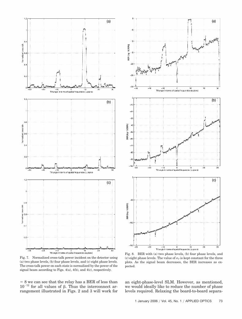
� 8 we can see that the relay has a BER of less than10 12 for all values of �. Thus the interconnect ar-rangement illustrated in Figs. 2 and 3 will work for
an eight-phase-level SLM. However, as mentioned,we would ideally like to reduce the number of phaselevels required. Relaxing the board-to-board separa-
Fig. 7. Normalized cross-talk power incident on the detector using(a) two phase levels, (b) four phase levels, and (c) eight phase levels.The cross-talk power on each state is normalized by the power of thesignal beam according to Figs. 4(a), 4(b), and 4(c), respectively.
Fig. 8. BER with (a) two phase levels, (b) four phase levels, and(c) eight phase levels. The value of �T is kept constant for the threeplots. As the signal beam decreases, the BER increases as ex-pected.
1 January 2006 � Vol. 45, No. 1 � APPLIED OPTICS 73
tion dPCB or changing the VCSEL pitch dp will reducethe cross talk. Also, we can look into ways of increas-ing the robustness of our active relay by using theconcept of multiple detectors per channel.
6. Conclusions
In this paper we have considered the design and op-eration of a telecentric adaptive optical link based ona linear array of VCSELs, a corresponding array ofdetectors, and a reconfigurable SLM that can steerthe signal beams to maintain alignment. The pri-mary aim of this analysis was to develop a modelcapable of predicting the performance of such an in-terconnect as a function of the number of SLM phaselevels and of the system geometry. To this end, weused a simple BER model related only to the opticalinterconnect, and the thermal noise was assumed todominate. The SLM diffraction efficiency as a func-tion of the number of phase levels, the incidentGaussian beam profile, and the position of the signalbeam (first diffraction order) in the detector planewere rigorously calculated. In addition, system pa-rameters, such as VCSEL pitch, SLM pixel size, SLMdimensions, and operating wavelength, were chosenbased on current technological capabilities. However,the model is flexible enough to accommodate non-standard geometries.
The model was then used to calculate the BER as afunction of tilt angle over a range of � � �0.6°. Theanalysis shows that there are two key effects thatdetermine the BER as a function of tilt error. First,the intrinsic roll-off in diffraction efficiency due tospace quantization that causes the signal power todrop off as we increase the tilt error; second, thepresence of higher diffraction orders from neighbor-ing channels. In the case of an interconnect based ontwo phase levels, there is a limited range over whichthe system can operate owing to the aforementionedlimitations. By increasing the number of phase levelsfrom two to four, we showed that the BER meets ourtarget value of 10 12 across the entire alignmentrange. This is due to two factors: an increase in effi-ciency and a reduction of higher diffraction orders.Thus, for a simple link in which there is a one-to-onecorrespondence between VCSELs and detectors, atleast a four-phase SLM, such as a nematic device, willbe the required. However, relaxing parameters suchas board-to-board separation dPCB and VCSEL pitchdp will increase the performance of the optical inter-connect even when binary holograms are used. Itshould be noted that for a fuller analysis, other noisesources, such as shot noise and the presence of thezeroth order in the replay field, must be taken intoaccount. Nonetheless, it is believed that our modelindicates the upper performance limit of an ideal de-vice in which the zeroth order is completely sup-pressed. Thus future research will focus ondeveloping a more realistic BER model, modelinglosses due to polarizers and other optical components,and fine-tuning changes in the parameters of thesystem layout, such as VCSEL pitch, to further re-
duce cross talk. In addition, we aim to experimentallydemonstrate such an adaptive optical link that isbased on LCOS SLM technology.
This research was conducted with the support ofthe Engineering and Physical Science ResearchCouncil (EPSRC). The National Council of Scienceand Technology of Mexico (CONACyT) supports thework of D. Gil Leyva. The authors thank John Carrollfor the mathematical discussions.
References1. A. Kirk, D. Plant, T. Symanski, Z. Vranesic, F. Tooley, D.
Rolston, M. Ayliffe, F. Lacroix, B. Robertson, E. Bernier, and D.Brosseau, “Design and implementation of a modulator-basedfree-space optical backplane for multiprocessor applications,”Appl. Opt. 42, 2465–2481 (2003).
2. T. Sakano, T. Matsumoto, and K. Noguchi, “Three-dimensionalboard-to-board free-space optical interconnects and their ap-plication to the prototype multiprocessor system: COSINE-III,” Appl. Opt. 39, 1815–1822 (1995).
3. F. A. P. Tooley, “Challenges in optically interconnecting elec-tronics,” IEEE J. Sel. Top. Quantum Electron. 2, 3–13 (1996).
4. R. K. Kostuk, “Simulation of board-level free-space optical in-terconnects for electronic processing,” Appl. Opt. 31, 2438–2445 (1992).
5. D. C. O’Brien, G. Faulkner, T. D. Wilkinson, B. Robertson, andD. Gil Leyva, “Design and analysis of an adaptive board toboard dynamic holographic interconnect,” Appl. Opt. 43, 3297–3305 (2004).
6. G. Boisset, B. Robertson, and H. Hinton, “Design and construc-tion of an active alignment demonstrator for a free space op-tical interconnect,” IEEE Photon. Technol. Lett. 7, 676–678(1995).
7. K. Hirabayashi, T. Yamamoto, S. Hino, Y. Kohama, and K.Tateno, “Optical beam direction compensation system forboard to board free space optical interconnection in high ca-pacity ATM switch,” J. Lightwave Technol. 14, 874–882(1997).
8. S. Lee, L. Huang, C. Kim, and M. Wu, “Free-space fiber opticsswitches based on MEMs vertical torsion mirrors,” J. Light-wave Technol. 17, 7–13 (1999).
9. D. P. Resler, D. S. Hobbs, R. C. Sharp, L. J. Friedman, andT. A. Dorschner, “High-efficiency liquid-crystal optical phase-array beam steering,” Opt. Lett. 21, 689–691 (1996).
10. W. A. Crossland, I. G. Manolis, M. M. Redmond, K. L. Tan,T. D. Wilkinson, M. J. Holmes, T. R. Parker, H. H. Chu, J.Croucher, V. A. Handerek, S. T. Warr, B. Robertson, I. Bonas,R. Franklin, C. Stace, H. J. White, R. A. Woolley, and G.Henshall, “Holographic optical switching: The ROSES Dem-onstrator,” J. Lightwave Technol. 17, 1845–1854 (2000).
11. See www.paralleloptics.com.12. J. Liesner, M. Reichter, and H. J. Tiziani, “Determination and
compensation of aberrations using SLMs,” Opt. Commun. 233,161–166 (2004).
13. D. Gil-Leyva, B. Robertson, C. J. Henderson, T. D. Wilkinson,D. C. O’Brien, and G. Faulkner, “Free space optical intercon-nect using a FLC SLM for active beam steering and wave frontcorrection,” in Micro-Optics, VCSELs and Photonic Intercon-nects, H. Thienpont, K. D. Choquette, and M. R. Taghizadeh,eds., Proc. SPIE 5453, 62–71 (2004).
14. F. B. McCormick and F. A. P. Tooley, “Optical and mechanicalissues in free-space digital optical logic systems,” in DesignIssues in Optical Processing, J. Lee, ed., Cambridge Studies inModern Optics (Cambridge U. Press, 1995), pp. 220–270.
15. K. L. Tan, S. T. Warr, I. G. Manolis, T. D. Wilkinson, M. M.Redmond, W. A. Crossland, R. J. Mears, and B. Robertson,
74 APPLIED OPTICS � Vol. 45, No. 1 � 1 January 2006

“Dynamic holography for optical interconnections. II. Routingholograms with predictable location and intensity of each dif-fraction order,” J. Opt. Soc. Am. A 18, 205–215 (2001).
16. V. Arrizon, E. Carreon, and M. Testorf, “Implementation ofFourier illuminators using pixelated SLM: efficiency limita-tions,” Opt. Commun. 160, 207–213 (1999).
17. J. W. Goodman, Introduction to Fourier Optics (McGraw-Hill,1968).
18. V. Morozov, J. Neff, H. Temkin, and A. Fedor, “Analysis of athree dimensional computer optical scheme based on bi-directional free space optical interconnects,” Opt. Eng. 34,523–534 (1995).
19. R. N. Bracewell, The Fourier Transform and Its Applications,3rd ed. (McGraw-Hill, 2000).
20. M. Johansson, S. Hard, B. Robertson, I. Manolis, T. D. Wilkin-son, and W. A. Crossland, “Adaptive beam steering imple-mented in an FLC-SLM free space optical switch,” Appl. Opt.41, 4904–4911 (2001).
21. W. H. Lee, “Binary computer-generated holograms,” Appl.Opt. 18, 3661–3669 (1979).
22. H. Dammann, “Blazed synthetic phase only holograms,” Optik31, 95–104 (1970).
23. P. O’Neil, Advanced Engineering Mathematics (Wadsworth,1983).
24. H. Hamam and J. L. de Bougrenet de la Tocnaye, “Diffractionefficiency of quantized programable phase elements: a criticalassessment,” Pure Appl. Opt. 5, 389–403 (1996).
25. C. J. Henderson, B. Robertson, D. Gil-Leyva, T. D. Wilkinson,D. C. O’Brien, and G. Faulkner, “Control of a free space adap-tive optical interconnect using a liquid crystal spatial lightmodulator for beam steering,” Opt. Eng. 44, 075401 (2005).
26. G. C. Boisset, “Optomechanics and optical packing for free-space optical interconnects,” Ph.D. thesis (McGill University,Montreal, Canada, 1997).
27. D. S. Steinberg, Vibration Analysis for Electronic Equipment,3rd ed. (Wiley-Interscience, 2000).
28. A. P. Sparks, R. C. Chittick, W. A. Crossland, and J. R. Brock-lehurst, “A 128 � 128 matrix electrically addressed ferroelec-tric liquid crystal spatial light modulator,” in Proceedings ofthe IEE Technical Digest (Institution of Electrical Engineers,1988), Vol. 121, pp. 28–32.
29. See http://www.commsdesign.com/.30. A. Yariv, Optical Electronics in Modern Communications (Ox-
ford U. Press, 1997).31. G. P. Agrawal, Fiber-Optic Communication Systems, 3rd ed.
(Wily-Interscience, 2002).32. R. Ramaswami and K. N. Sivarajan, Optical Networks (Mor-
gan Kaufman, 2002).
1 January 2006 � Vol. 45, No. 1 � APPLIED OPTICS 75