Embed Size (px)
Citation preview

Critical Charge and SET Pulse Widths for Combinational Logic in Commercial 90nm CMOS Technology
Riaz Naseer, Jeff Draper, Younes Boulghassoul Information Sciences Institute
University of Southern California Marina Del Rey, CA 90292 USA
Sandeepan DasGupta, Art Witulski Institute for Space and Defense Electronics
Vanderbilt University Nashville, TN 37235-1553 USA
ABSTRACT This work presents an efficient hybrid simulation approach, developed for accurate characterization of single-event transients (SETs) in combinational logic. Using this approach, we show that charges as small as 3.5fC can introduce transients in commercial 90nm CMOS technology, hence increasing the likelihood of SET-induced soft errors. SET pulse-widths as large as 942ps are predicted at an LET (Linear Energy Transfer) of 60MeV-cm2/mg. Process-corner variations are shown to modulate SET pulse-widths by up-to 75%. The results suggest that selection of mitigation techniques for SET radiation-hardened circuits cannot exclusively rely on baseline process analyses, as they might grossly underestimate the true SET risk to the design.
Categories and Subject Descriptors B.7.2 [Hardware]: Design Aids – simulation
General Terms: Reliability
Keywords Critical Charge, Single Event Transient, Soft Error
1. INTRODUCTION Soft errors are a major reliability concern for today’s deep sub-micron technologies. Single Event Upsets (SEUs) were long recognized as a reliability concern, and there have been a number of solutions presented to mitigate SEU effects [2]. Single Event Transients (SETs), on the other hand, were not considered significant due to logical, electrical and latching window masking phenomenon present in digital combinational logic. However, with technology scaling, reduced nodal capacitances and lower supply voltages decrease the minimal charge required to introduce a transient in combinational logic. Also, the higher operating frequencies make it more likely that a SET generated in combinational logic will be captured at the storage element. Therefore, it is predicted that SETs will soon outpace the soft error rate caused by SEU [7].
Numerous efforts have been made to indirectly characterize SETs
through experimentation [1][7][9]. A more recent effort by Ferlet-Cavrois et al [8] succeeded in measuring transient current pulses on relatively large devices in real-time conditions. This direct measurement approach remains considerably challenging as it tackles issues related to probe capacitance isolation from DUT (Device under Test) measurements and large scope sampling frequency requirements for very small transients capture. Additionally, experimental irradiation of test devices remains very costly and requires extensive time and engineering resources. So, attempting to experimentally characterize SET profiles for every standard cell gate used in a commercial ASIC library is not a viable option. On the other hand, conservative estimations about SET profiles may result in over-design efforts and large performance penalties. As an alternative to experimentation, 3D mixed-mode simulations have been shown to accurately predict upset effects from single event strikes [5]. Furthermore, extensive 3D mixed-mode simulations have been performed on minimum-size inverters for technologies from 0.25μm to 100nm [6], yet no data is available on various ASIC gates for commercial 90nm CMOS processes.
In this paper, a hybrid simulation approach to characterize SET pulses is employed. The method used combines the advantages of 3D device simulations and SPICE circuit simulations. In particular, we use 3D device simulations to characterize current pulses for ion strikes and later these pulses are used as inputs to SPICE circuit simulations for the emulation of ion strikes on standard cells in a commercial ASIC library. Furthermore, the minimum charges that can induce propagating transients have been investigated.
For ion strikes with relatively large LET values, it is observed that SET pulses are wide enough to propagate through any number of stages, undampened. Additionally, the effects of parametric variations, such as process corners and fan-out, are also investigated because of their ability to noticeably modulate the SET pulse widths. It is observed that SET pulse widths at the 90nm technology node are relatively smaller than those observed in older technologies such as 0.25μm and 0.18µm. This SET pulse characterization helps in identifying the severity of soft error problem caused by transients and provide guidelines for performance penalties of different SET mitigation techniques.
In section 2, we describe proposed simulation methodology. Section 3 discusses critical charge concepts for combinational logic gates. Section 4 presents simulation results for SET pulse widths; describes effects of parametric variations and compares results with published data. Section 5 concludes the paper.
Permission to make digital or hard copies of all or part of this work for personal or classroom use is granted without fee provided that copies are not made or distributed for profit or commercial advantage and that copies bear this notice and the full citation on the first page. To copy otherwise, or republish, to post on servers or to redistribute to lists, requires prior specific permission and/or a fee. 2. SIMULATION METHODOLOGY GLSVLSI’07, March 11–13, 2007, Stresa-Lago Maggiore, Italy. Copyright 2007 ACM 978-1-59593-605-9/07/0003...$5.00.
In contrast to previous work, we propose a hybrid simulation approach to characterize the single-event transient phenomenon in
227
combinational logic. This approach consists of utilizing 3D device simulations to model ion strikes on target devices and SPICE circuit simulations to study SET generation and propagation through combinational logic. This hybrid approach speeds up the SET characterization process by orders of magnitude as compared to traditional 3D mixed-mode simulations. Furthermore, it provides the flexibility to inject transient current pulses anywhere in a large circuit and directly observe the propagation of the resulting transient through a large combinational network. In other words, this approach combines the proven accuracy in ion strike modeling of 3D device simulations [5] and the efficiency of commercial circuit simulators such as SPICE.
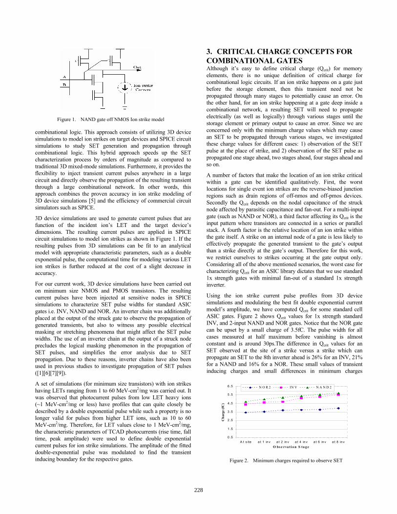
3D device simulations are used to generate current pulses that are function of the incident ion’s LET and the target device’s dimensions. The resulting current pulses are applied in SPICE circuit simulations to model ion strikes as shown in Figure 1. If the resulting pulses from 3D simulations can be fit to an analytical model with appropriate characteristic parameters, such as a double exponential pulse, the computational time for modeling various LET ion strikes is further reduced at the cost of a slight decrease in accuracy.
For our current work, 3D device simulations have been carried out on minimum size NMOS and PMOS transistors. The resulting current pulses have been injected at sensitive nodes in SPICE simulations to characterize SET pulse widths for standard ASIC gates i.e. INV, NAND and NOR. An inverter chain was additionally placed at the output of the struck gate to observe the propagation of generated transients, but also to witness any possible electrical masking or stretching phenomena that might affect the SET pulse widths. The use of an inverter chain at the output of a struck node precludes the logical masking phenomenon in the propagation of SET pulses, and simplifies the error analysis due to SET propagation. Due to these reasons, inverter chains have also been used in previous studies to investigate propagation of SET pulses ([1][6][7][9]).
A set of simulations (for minimum size transistors) with ion strikes having LETs ranging from 1 to 60 MeV-cm2/mg was carried out. It was observed that photocurrent pulses from low LET heavy ions (~1 MeV-cm2/mg or less) have profiles that can quite closely be described by a double exponential pulse while such a property is no longer valid for pulses from higher LET ions, such as 10 to 60 MeV-cm2/mg. Therefore, for LET values close to 1 MeV-cm2/mg, the characteristic parameters of TCAD photocurrents (rise time, fall time, peak amplitude) were used to define double exponential current pulses for ion strike simulations. The amplitude of the fitted double-exponential pulse was modulated to find the transient inducing boundary for the respective gates.
3. CRITICAL CHARGE CONCEPTS FOR COMBINATIONAL GATES
Figure 1. NAND gate off NMOS Ion strike model
Although it’s easy to define critical charge (Qcrit) for memory elements, there is no unique definition of critical charge for combinational logic circuits. If an ion strike happens on a gate just before the storage element, then this transient need not be propagated through many stages to potentially cause an error. On the other hand, for an ion strike happening at a gate deep inside a combinational network, a resulting SET will need to propagate electrically (as well as logically) through various stages until the storage element or primary output to cause an error. Since we are concerned only with the minimum charge values which may cause an SET to be propagated through various stages, we investigated these charge values for different cases: 1) observation of the SET pulse at the place of strike, and 2) observation of the SET pulse as propagated one stage ahead, two stages ahead, four stages ahead and so on.
A number of factors that make the location of an ion strike critical within a gate can be identified qualitatively. First, the worst locations for single event ion strikes are the reverse-biased junction regions such as drain regions of off-nmos and off-pmos devices. Secondly the Qcrit depends on the nodal capacitance of the struck node affected by parasitic capacitance and fan-out. For a multi-input gate (such as NAND or NOR), a third factor affecting its Qcrit is the input pattern where transistors are connected in a series or parallel stack. A fourth factor is the relative location of an ion strike within the gate itself. A strike on an internal node of a gate is less likely to effectively propagate the generated transient to the gate’s output than a strike directly at the gate’s output. Therefore for this work, we restrict ourselves to strikes occurring at the gate output only. Considering all of the above mentioned scenarios, the worst case for characterizing Qcrit for an ASIC library dictates that we use standard 1x strength gates with minimal fan-out of a standard 1x strength inverter.
Using the ion strike current pulse profiles from 3D device simulations and modulating the best fit double exponential current model’s amplitude, we have computed Qcrit for some standard cell ASIC gates. Figure 2 shows Qcrit values for 1x strength standard INV, and 2-input NAND and NOR gates. Notice that the NOR gate can be upset by a small charge of 3.5fC. The pulse width for all cases measured at half maximum before vanishing is almost constant and is around 30ps.The difference in Qcrit values for an SET observed at the site of a strike versus a strike which can propagate an SET to the 8th inverter ahead is 26% for an INV, 21% for a NAND and 16% for a NOR. These small values of transient inducing charges and small differences in minimum charges
0 .5
1 .5
2 .5
3 .5
4 .5
5 .5
6 .5
A t s ite a t 1 in v a t 2 in v a t 4 in v a t 6 in v a t 8 in vO bs e rva ti o n S ta g e
Cha
rge
(fC
)
N O R 2 IN V N A N D 2
Figure 2. Minimum charges required to observe SET
228

50
250
450
650
850
5 15 25 35 45 55 65LET (Me V -cm 2 /m g )
SET
Pulse
Wid
th (p
s)
IN V N A N D N O R
Figure 4. SET Pulse Width with Process Corner Variations
0
1 0 0
2 0 0
3 0 0
4 0 0
5 0 0
6 0 0
7 0 0
0 1 0 2 0 3 0 4 0 5 0 6 0 7 0L ET ( M e V - c m 2 /m g )
SET
Pulse
Wid
th (p
s)
IN V N A N D 2 N O R 2
Figure 3. SET Pulse Widths for large LET strikes on ASIC gates
required to propagate SETs to various stages has implications for SET mitigation techniques which rely on gate sizing to improve reliability, such as [3],[4], and [12].
4. SET PULSE WIDTHS for LARGE LETs Photocurrents from high LET ion strikes have been directly applied at relevant circuit nodes on the investigated ASIC gates. The resulting transients from these large LET ion strikes have a quick charge collection phase. This quick response time causes the drain-substrate junction to forward-bias and the voltage at the struck node to undershoot significantly. This effect is typical for bulk CMOS processes and has also been observed in [6]. Another observation for SETs generated from these strikes is that the resulting transients quickly settle down (just after 2nd inverter) to a perfect square wave and their pulse widths after the 3rd inverter is constant. Figure 3 provides the widths of SETs from large LET ions. These values have been obtained using minimum strength inverter chain at the output of struck gate with fan-out of 1.
Notice that the parallel stack of reverse-biased regions exhibits the highest vulnerability to ion strikes. This fact is evident from the sensitivity of NOR gate for these off-nmos strikes compared to INV and NAND gates. Results show that generated SETs could be as large as 653ps for an LET of 60MeV-cm2/mg for NOR gates. As expected, this also confirms that larger LETs result in larger pulse widths. It is interesting to note that the SET pulse widths predicted from these simulations are relatively smaller than observed for earlier technology nodes in [1][7][9]. Although a direct comparison with transient current measurements reported in [8] cannot be made because of very large size devices under test and a different technology used in that work (50nm), our simulations agree with the trend that SET pulse widths are getting smaller in sub-100nm technologies. This has strong implications for SET mitigation techniques which require temporal filtering such as DF-DICE [11] and Temporal Sampling Latch [10]. As the performance penalties of these techniques are directly proportional to the SET pulse widths to
be filtered, these techniques can be applied with reasonable penalties in modern technologies.
4.1 Process Corner Variations We have modeled the following process corners for this study: FF (Fast NMOS, Fast PMOS), FS (Fast NMOS, Slow PMOS), SF (Slow NMOS, Fast PMOS), SS (Slow NMOS, Slow PMOS) and TT (Typical NMOS, Typical PMOS). Figure 4 shows the spread in SET pulse widths around the TT process corner. The SS corner results in the largest pulse width while the FF corner yields the smallest for these off-nmos strikes. The pulse widths reported are the settled pulse widths at the output of the 3rd inverter from the location of the strike.
From Figure 4, we see that the worst case SET pulse width at an LET of 60MeV-cm2/mg could be as large as 885ps. The worst case percentage variations between the extreme process corners for a particular gate are in the range of 42% to 75%. For example, the percentage variation of SET pulse width for the inverter is 42% for LET of 10MeV-cm2/mg and 75% for LET of 60MeV-cm2/mg. The NOR gate, on the other hand, shows a variation of 50% to 70% for the same cases. Considering this range of up to 75% variation in the SET pulse widths for different process corners, it can be concluded that SET pulse widths are very sensitive to process corners. This quite large variation needs to be taken into account while analyzing performance penalties of SET mitigation techniques.
4.2 Fan-out Variations This sub-section analyzes the effects of fan-out variations on SET pulse widths. Table I shows the simulation results with fan-out variations ranging from 1 to 6. The upper limit of 6 on fan-out is chosen due to the drive capability of minimum size gates. An interesting observation can be made from these results: a larger fan-out result in generating larger SET pulse widths. This anomaly is best explained by a close look at the waveforms of the struck node. These large LET ion strikes deposit significant charge in very short
TABLE I. FAN-OUT VARIATIONS ON SET PULSE-WIDTHS FOR DIFFERENT GATES AND LET
LET = 10 MeV-cm2/mg LET= 20 MeV-cm2/mg LET= 40 MeV-cm2/mg LET= 50 MeV-cm2/mg LET= 60 MeV-cm2/mg
FO INV NAND NOR INV NAND NOR INV NAND NOR INV NAND NOR INV NAND NOR
1 120 125 201 151 157 271 225 244 496 254 263 571 286 295 654
2 142 146 240 176 182 318 260 268 559 291 299 638 324 333 725
4 176 179 310 217 222 400 316 324 664 350 357 750 387 395 843
6 180 180 370 239 240 469 358 363 752 395 400 843 435 442 942
229

time which result in undershoots that attain voltages as low as the negative of the supply rail. A large nodal capacitance in this scenario actually slows down the charge collection phase and result in widening the SET pulse width while reducing the amplitude of undershoots.
From the results it can be observed that fan-out has a significant effect on SET pulse-widths and can vary the SET pulse width by as large as 84% for the NOR gate. Fan-out configurations for a gate being different in a synthesized logic, it is necessary to characterize transients with SET affecting parameters.
4.3 Comparison with Published Data This sub-section correlates our simulation results with SET data available from irradiation testing as well as 3D mixed-mode simulations presented in prior research. Due to the fact that irradiation testing and simulations were conducted on different technology nodes and used different device sizes, it is difficult to make direct comparisons with published data. Yet, we can identify relevant general trends, allowing some grounds for joint analyses and discussions.
The graph in Figure 5 plots the SET pulse width versus LET for different experiments including our simulation results for INV and NOR gates. The NAND results are similar to those of the inverter and hence are not plotted to improve the graph’s readability. It should be noticed that all previous studies have used inverter as the target device. As can be seen from the graph, our hybrid simulation results for the inverter case relate well to the 3D mixed-mode simulation results of Dodd et al for 100nm modeled technology node [6]. More importantly, the trend showing a SET pulse width decrease with technology scaling, observed by Dodd et al and later confirmed through direct measurement of transient currents by Ferlet-Cavrios et al [8], is similarly present in our results, further validating the applicability of the hybrid simulation approach presented in this paper. SET pulse widths from NOR gate also follow a comparable trend, but as mentioned earlier, the NOR gate is much more sensitive to radiation and its resulting transients are much wider.
5. CONCLUSION An efficient hybrid simulation approach is proposed to model single event transients in combinational networks. This approach combines the accuracy benefits of 3D device simulations in modeling ion strikes, and computation time efficiency and ability to simulate large circuits of commercial SPICE type circuit simulators. Minimal charges that can induce single event transients on some commercial 90nm ASIC library cells have been computed using this simulation approach. Current nanometer technologies are shown to be very
sensitive to radiation, where charges as small as 3.5fC are capable of inducing a transient increasing the likelihood of soft errors. Process corner and fan-out variations strongly affect SET pulse widths. SET pulse widths can vary as large as 75% for a particular gate between extreme process corners. The large fan-out for large LETs results in slowing the charge collection and hence can widen the transients by as much as 84%.
Compared to earlier work on 0.25μm and 0.18μm technologies, the SET pulse widths predicted here are relatively smaller. It should be noted that the scaling-driven reduction in SET pulse width does not necessarily translate into a decrease in the error contribution of SETs, since higher operating frequencies in scaled technologies make it more likely for these SETs to be latched in storage elements. However, the relative decrease in transient pulse widths may revive the interest in adopting transient filtering solutions as part of the radiation hardening techniques. The associated performance penalties for SET mitigation, thus far significantly large, may become less intrusive to the circuit’s optimal operations.
6. REFERENCES [1] Benedetto, J., et al Heavy ion-induced digital single-event
transients in deep submicron Processes. IEEE Trans on Nuc. Sci. V. 51, Issue 6, Dec. 2004, 3480 – 3485
[2] Chakraborty, K., Mazumder, P. Fault-Tolerance and Reliability Techniques for High-Density Random-Access Memories. Prentice Hall, 1st edition, Jun 2002
[3] Deogun, H.S., Sylvester, D., Blaauw, D. Gate-level mitigation techniques for neutron-induced soft error rate. ISQED 2005, 175 – 180
[4] Dhillon, Y.S., Diril, A.U., Chatterjee, A. Soft-error tolerance analysis and optimization of nanometer circuits. DATE Proceedings 2005, 288 - 293 V. 1
[5] Dodd, P.E., et al SEU-sensitive volumes in bulk and SOI SRAMs from first-principles calculations and experiments. IEEE Trans. on Nuc. Sci., V. 48, Dec. 2001, 1893 - 1903
[6] Dodd, P.E., et al Production and propagation of single-event transients in high-speed digital logic ICs. IEEE Trans. on Nuc Sci., V. 51, Issue 6, Dec. 2004, 3278 – 3284
[7] Eaton, P., et al Single event transient pulse width measurements using a variable temporal latch technique. IEEE Trans. on Nuc. Sci. V. 51, Dec. 2004, 3365 – 3368
[8] Ferlet-Cavrois, V., et al Direct measurement of transient pulses induced by laser and heavy ion irradiation in deca-nanometer devices. IEEE Trans. on Nuc Sci V.52, Dec. 2005
[9] Gadlage, M.J., et al Single event transient pulse widths in digital microcircuits. IEEE Trans. on Nuc Sci V. 51, Issue 6, Part 2, Dec. 2004, 3285 – 3290
[10] Mavis, D.G., Eaton, P.H. Soft error rate mitigation techniques for modern microcircuits. Reliability Physics Symposium Proceedings, 2002, 216 – 225
[11] Naseer, R., Draper, J. The DF-DICE storage element for immunity to soft errors. 48th MWSCAS 2005, 303 – 306
[12] Zhou, Q., Mohanram, K. Transistor sizing for radiation hardening. Reliability Physics Symposium Proceedings, 2004, 310 – 315
0
2 0 0
4 0 0
6 0 0
8 0 0
1 0 0 0
1 2 0 0
1 4 0 0
1 6 0 0
1 8 0 0
0 2 0 4 0 6 0 8L ET ( M e V - c m 2 /m g )
SET
Pulse
Wid
th (p
s)
0
G a d la g e 0 .1 8 u m
D o d d 0 .1 0 u m
Ea to n 0 .1 8 u m
IN V 9 0 n m
N O R 9 0 n m
Figure 5. SET Pulse Width Comparison
230