Embed Size (px)
Citation preview

CPE 323 Introduction to Embedded Computer Systems:ADC12 and DAC12
Instructor: Dr Aleksandar MilenkovicLecture Notes

CPE 323 2
Outline
MSP430: System Architecture ADC12 Module DAC12 Module

CPE 323 3
ADC12 Introduction ADC12 module supports fast, 12-bit analog-to-digital conversions
12-bit SAR core, sample select control, reference generator and a 16 word conversion-and-control buffer.
Conversion-and-control buffer allows up to 16 independent ADC samples to be converted and stored without any CPU intervention
ADC12 features include Greater than 200 ksps maximum conversion rate Monotonic 12-bit converter with no missing codes Sample-and-hold with programmable sampling periods controlled by software or timers. Conversion initiation by software, Timer_A, or Timer_B Software selectable on-chip reference voltage generation (1.5 V or 2.5 V) Software selectable internal or external reference Eight individually configurable external input channels Conversion channels for internal temperature sensor, AVCC, and external references Independent channel-selectable reference sources for both positive and negative
references Selectable conversion clock source Single-channel, repeat-single-channel, sequence, and repeat-sequence conversion modes ADC core and reference voltage can be powered down separately Interrupt vector register for fast decoding of 18 ADC interrupts 16 conversion-result storage registers

CPE 323 4
ADC12 Block Diagram

CPE 323 5
ADC Core
Core converts an analog input to its 12-bit digital representation an stores the result in conversion memory; the conversion formula is
VR+ and VR− are programmable voltage levels: the upper (VR+) and lower limits (VR-) of the conversion
The digital output (NADC) is full scale (0FFFh) when the input signal is equal to or higher than VR+
0h when the input signal is equal to or lower than VR− The input channel and the reference voltage levels (VR+ and VR−)
are defined in the conversion-control memory.
RR
RinADC VV
VVN 4095

CPE 323 6
Core Configuration
Two control registers, ADC12CTL0 and ADC12CTL1 The core is enabled with the ADC12ON bit
The ADC12 can be turned off when not in use to save power With few exceptions the ADC12 control bits can only be
modified when ENC = 0 ENC must be set to 1 before any conversion can take place

CPE 323 7
Conversion Clock Selection
ADC12CLK is used both as the conversion clock and to generate the sampling period when the pulse sampling mode is selected
Source clock selection ADC12SSELx bits to select a source: SMCLK, MCLK, ACLK,
and the internal oscillator ADC12OSC The ADC12OSC, generated internally, is in the 5-MHz range, but
varies with individual devices, supply voltage, and temperature See the device-specific datasheet for the ADC12OSC specification
Source clock can be divided from 1-8 using the ADC12DIVx bits The user must ensure that the clock chosen for ADC12CLK
remains active until the end of a conversion. If the clock is removed during a conversion, the operation will not complete and any result will be invalid
CPE 323 8
ADC12 Inputs The eight external and four internal analog signals are selected as the
channel for conversion by the analog input multiplexer The input multiplexer is a break-before-make type to reduce input-to-input
noise injection resulting from channel switching as shown below
Port selection ADC12 inputs are multiplexed with the port P6 pins, which are
digital CMOS gates Parasitic current problem
When analog signals are applied to digital CMOS gates, parasitic current can flow from VCC to GND. This parasitic current occurs if the input voltage is near the transition level of the gate.
Disabling the port pin buffer eliminates the parasitic current flow and therefore reduces overall current consumption. The P6SELx bits provide the ability to disable the port pin input and output buffers

CPE 323 9
Voltage Reference Generator
Built-in voltage reference with two selectable voltage levels, 1.5 V and 2.5 V
Either may be used internally (REFON=1) and externally on pin VREF+ When REF2_5V = 1, the internal reference is 2.5 V When REF2_5V = 0, the reference is 1.5 V The reference can be turned off to save power when not in use For proper operation the internal voltage reference generator must be
supplied with storage capacitance across VREF+ and AVSS. The recommended storage capacitance is a parallel combination of 10-μF and 0.1-μF capacitors
From turn-on, a minimum of 17 ms must be allowed for the voltage reference generator to bias the recommended storage capacitors.
External references may be supplied for VR+ and VR− through pins VeREF+ and VREF−/VeREF− respectively
CPE 323 10
Auto Power-down
Designed for low power applications When the ADC12 is not actively converting, the core is
automatically disabled and automatically re-enabled when needed.
The ADC12OSC is also automatically enabled when needed and disabled when not needed.
The reference is not automatically disabled, but can be disabled by setting REFON = 0. When the core, oscillator, or reference are disabled, they consume no current

CPE 323 11
Sample Timing
An analog-to-digital conversion is initiated with a rising edge of the sample input signal SHI
The source for SHI is selected with the SHSx bits and includes the following:
The ADC12SC bit The Timer_A Output Unit 1 The Timer_B Output Unit 0 The Timer_B Output Unit 1
The polarity of the SHI signal source can be inverted with the ISSH bit.
The SAMPCON signal controls the sample period and start of conversion. When SAMPCON is high, sampling is active. The high-to-low SAMPCON transition starts the analog-to-digital conversion, which requires 13 ADC12CLK cycles.
Two different sample-timing methods are defined by control bit SHP, extendedsample mode and pulse mode.

CPE 323 12
Extended Sample Mode
Selected when SHP = 0 The SHI signal directly controls SAMPCON and defines
the length of the sample period tsample When SAMPCON is high, sampling is active The high-to-low SAMPCON transition starts the conversion after
synchronization with ADC12CLK

CPE 323 13
Pulse Sample Mode Selected when SHP = 1 The SHI signal is used to trigger the sampling timer The SHT0x and SHT1x bits in ADC12CTL0 control the interval of the
sampling timer that defines the SAMPCON sample period tsample. The sampling timer keeps SAMPCON high after synchronization with
AD12CLK for a programmed interval tsample. The total sampling time is tsample plus tsync.
The SHTx bits select the sampling time in 4x multiples of ADC12CLK. SHT0x selects the sampling time for ADC12MCTL0 to 7 and SHT1x selects the sampling time for ADC12MCTL8 to 15.

CPE 323 14
Sample Time Consideration
When SAMPCON = 0 all Ax inputs are high impedance When SAMPCON = 1, the selected Ax input can be modeled as an RC low-
pass filter during the sampling time tsample (see below) An internal MUX-on input resistance RI (max. 2 kΩ) in series with capacitor
CI (max. 40 pF) is seen by the source. The capacitor CI voltage VC must be charged to within LSB of the source voltage VS for an accurate 12-bit conversion
tsample > (RS+RI)ln(213)CI + 800ns tsample > (RS+ 2k)9.011x40pF + 800ns;
if RS is 10 kΩ, tsample must be greater than 5.13 μs.

CPE 323 15
Conversion Memory
16 ADC12MEMx conversion memory registers to store conversion results
Each ADC12MEMx is configured with an associated ADC12MCTLx control register

CPE 323 16
Conversion Memory (cont’d)
SREFx bits define the voltage reference INCHx bits select the input channel EOS bit defines the end of sequence when a sequential conversion
mode is used A sequence rolls over from ADC12MEM15 to ADC12MEM0 when the
EOS bit in ADC12MCTL15 is not set CSTARTADDx bits define the first ADC12MCTLx used for any
conversion If the conversion mode is single-channel or repeat-single-channel the
CSTARTADDx points to the single ADC12MCTLx to be used If the conversion mode selected is either sequence-of-channels or
repeat-sequence-of-channels, CSTARTADDx points to the first ADC12MCTLx location to be used in a sequence.
A pointer, not visible to software, is incremented automatically to the next ADC12MCTLx in a sequence when each conversion completes. The sequence continues until an EOS bit in ADC12MCTLx is processed - this is the last control byte processed.
When conversion results are written to a selected ADC12MEMx, the corresponding flag in the ADC12IFGx register is set

CPE 323 17
Conversion Modes
Determined by CONSEQx bits

CPE 323 18
Single-Channel, Single Conversion Mode
A single channel is sampled and converted once
The ADC result is written to the ADC12MEMx defined by the CSTARTADDx bits.
When ADC12SC triggers a conversion, successive conversions can be triggered by the ADC12SC bit.
When any other trigger source is used, ENC must be toggled between each conversion.

CPE 323 19
Sequence-of-Channels Mode
A sequence of channels is sampled and converted once.
The ADC results are written to the conversion memories starting with the ADCMEMx defined by the CSTARTADDx bits.
The sequence stops after the measurement of the channel with a set EOS bit.
When ADC12SC triggers a sequence, successive sequences can be triggered by the ADC12SC bit.
When any other trigger source is used, ENC must be toggled between each sequence.

CPE 323 20
Repeat-Single-Channel Mode
A single channel is sampled and converted continuously.
The ADC results are written to the ADC12MEMx defined by the CSTARTADDx bits.
It is necessary to read the result after the completed conversion because only one ADC12MEMx memory is used and is overwritten by the next conversion.

CPE 323 21
Repeat-Sequence-of-Channels Mode
A sequence of channels is sampled and converted repeatedly.
The ADC results are written to the conversion memories starting with the ADC12MEMx defined by the CSTARTADDx bits.
The sequence ends after the measurement of the channel with a set EOS bit and the next trigger signal re-starts the sequence.

CPE 323 22
Using the Multiple Sample and Convert (MSC) Bit
Perform successive conversions automatically and as quickly as possible, a multiple sample and convert function is available
When MSC = 1, CONSEQx > 0, and the sample timer is used, the first rising edge of the SHI signal triggers the first conversion.
Successive conversions are triggered automatically as soon as the prior conversion is completed.
Additional rising edges on SHI are ignored until the sequence is completed in the single-sequence mode or until the ENC bit is toggled in repeat-single-channel, or repeated-sequence modes.
The function of the ENC bit is unchanged when using the MSC bit.

CPE 323 23
Stopping Conversions
Depends on the mode of operation. Recommended ways to stop an active conversion or
conversion sequence are Resetting ENC in single-channel single-conversion mode stops
a conversion immediately and the results are unpredictable. For correct results, poll the busy bit until reset before clearing ENC.
Resetting ENC during repeat-single-channel operation stops the converter at the end of the current conversion.
Resetting ENC during a sequence or repeat-sequence mode stops the converter at the end of the sequence.
Any conversion mode may be stopped immediately by setting the CONSEQx = 0 and resetting ENC bit. Conversion data are unreliable.
CPE 323 24
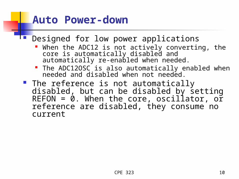
Temperature On-Chip Sensor
Select INCHx = 1010 Typical transfer function
(check device specific datasheet)
The sample period must be greater than 30 μs.
Selecting the temperature sensor automatically turns on the on-chip reference generator as a voltage source for the temperature sensor
However, it does not enable the VREF+ output or affect the reference selections for the conversion.
The reference choices for converting the temperature sensor are the same as with any other channel.

CPE 323 25
ADC Grounding and Noise Considerations

CPE 323 26
ADC Interrupts
The ADC12 has 18 interrupt sources: ADC12IFG0-ADC12IFG15 ADC12OV, ADC12MEMx overflow ADC12TOV, ADC12 conversion time overflow
The ADC12IFGx bits are set when their corresponding ADC12MEMx memory register is loaded with a conversion result.
An interrupt request is generated if the corresponding ADC12IEx bit and the GIE bit are set.
The ADC12OV condition occurs when a conversion result is written to any ADC12MEMx before its previous conversion result was read
The ADC12TOV condition is generated when another sample-and-conversion is requested before the current conversion is completed.

CPE 323 27
Interrupt Handling Routine The ADC12IV value is added to
the PC to automatically jump to the appropriate routine.
The numbers at the right margin show the necessary CPU cycles for each instruction.
The software overhead for different interrupt sources includes interrupt latency and return-from-interrupt cycles, but not the task handling itself
The latencies are: ADC12IFG0 - ADC12IFG14,
ADC12TOV and ADC12OV 16 cycles
ADC12IFG15 14 cycles The interrupt handler for
ADC12IFG15 shows a way to check immediately if a higher prioritized interrupt occurred during the processing of ADC12IFG15.
This saves nine cycles if another ADC12 interrupt is pending.

CPE 323 28
An Example: ADC12, Single Sample
//*****************************************************************//MSP430xG461x Demo - ADC12, Sample A0, Set P5.1 if A0 > 0.5*AVcc////Description: A single sample is made on A0 with reference to AVcc.//Software sets ADC12SC to start sample and conversion - ADC12SC//automatically cleared at EOC. ADC12 internal oscillator times sample (16x)// and conversion. In Mainloop MSP430 waits in LPM0 to save power until ADC12// conversion complete, ADC12_ISR will force exit from LPM0 in Mainloop on// reti. If A0 > 0.5*AVcc, P5.1 set, else reset.// ACLK = 32kHz, MCLK = SMCLK = default DCO 1048576Hz, ADC12CLK = ADC12OSC//// MSP430xG461x// -----------------// /|\| XIN|-// | | | 32kHz// --|RST XOUT|-// | |// Vin -->|P6.0/A0 P5.1|--> LED//// A. Dannenberg/ M. Mitchell// Texas Instruments Inc.// October 2006// Built with CCE Version: 3.2.0 and IAR Embedded Workbench Version: 3.41A//*****************************************************************#include "msp430xG46x.h"
void main(void){ WDTCTL = WDTPW + WDTHOLD; // Stop WDT ADC12CTL0 = SHT0_2 + ADC12ON; // Sampling time, ADC12 on ADC12CTL1 = SHP; // Use sampling timer ADC12IE = 0x01; // Enable interrupt ADC12CTL0 |= ENC; P6SEL |= 0x01; // P6.0 ADC option select P5DIR |= 0x02; // P5.1 output
while (1) { ADC12CTL0 |= ADC12SC; // Start sampling/conversion __bis_SR_register(LPM0_bits + GIE);
// LPM0, ADC12_ISR will force exit }}
#pragma vector = ADC12_VECTOR__interrupt void ADC12_ISR(void){ if (ADC12MEM0 >= 0x7ff) // ADC12MEM = A0 > 0.5AVcc? P5OUT |= 0x02; // P5.1 = 1 else P5OUT &= ~0x02; // P5.1 = 0
__bic_SR_register_on_exit(LPM0_bits); // Exit LPM0}

DAC12
CPE 323 30
DAC12 Introduction
12-bit, voltage output DAC. The DAC12 can be configured in 8-bit or 12-bit mode and may
be used in conjunction with the DMA controller When multiple DAC12 modules are present, they may be
grouped together for synchronous update operation. Features of the DAC12 include:
12-bit monotonic output 8-bit or 12-bit voltage output resolution Programmable settling time vs power consumption Internal or external reference selection Straight binary or 2s compliment data format Self-calibration option for offset correction Synchronized update capability for multiple DAC12s

CPE 323 31
DAC12 Block Diagram

CPE 323 32
DAC12 Core
DAC12RES 0 – 12-bit 1 – 8-bit
DAC12IR 0 – 3x 1 – 1x

CPE 323 33
DAC12 Port Selection
DAC12 outputs are multiplexed with the port P6 pins and ADC12 analog inputs, and also the VeREF+ and P5.1/S0/A12 pins
When DAC12AMPx > 0, the DAC12 function is automatically selected for the pin, regardless of the state of the associated PxSELx and PxDIRx bits.
The DAC12OPS bit selects between the P6 pins and the VeREF+ and P5.1 pins for the DAC outputs.
For example, when DAC12OPS = 0, DAC12_0 outputs on P6.6 and DAC12_1 outputs on P6.7.
When DAC12OPS = 1, DAC12_0 outputs on VeREF+ and DAC12_1 outputs on P5.1.
See the port pin schematic in the device-specific datasheet for more details.

CPE 323 34
DAC12 Reference
On MSP430FG43x and MSP430FG461x devices, the reference for the DAC12 is configured to use either an external reference voltage or the internal 1.5-V/2.5-V reference from the ADC12 module with the DAC12SREFx bits
When DAC12SREFx = {0,1} the VREF+ signal is used as the reference and when DAC12SREFx = {2,3} the VeREF+ signal is used as the reference
To use an ADC internal reference, it must be enabled and configured via the applicable ADC control bits.
DAC12 voltage output buffers Reference input and voltage output buffers of the DAC12 can be
configured for optimized settling time vs power consumption Eight combinations are selected using the DAC12AMPx bits.
In the low/low setting, the settling time is the slowest, and the current consumption of both buffers is the lowest.
The medium and high settings have faster settling times, but the current consumption increases.
See the device-specific data sheet for parameters.

CPE 323 35
Updating the DAC12 Voltage Output
DAC12_xDAT register can be connected directly to the DAC12 core or
double buffered. The trigger for updating the DAC12 voltage output is
selected with the DAC12LSELx bits. When DAC12LSELx = 0 the data latch is transparent and the
DAC12_xDAT register is applied directly to the DAC12 core. The DAC12 output updates immediately when new DAC12 data is written to the DAC12_xDAT register, regardless of the state of the DAC12ENC bit.
When DAC12LSELx = 1, DAC12 data is latched and applied to the DAC12 core after new data is written to DAC12_xDAT.
When DAC12LSELx = 2 or 3, data is latched on the rising edge from the Timer_A CCR1 output or Timer_B CCR2 output respectively. DAC12ENC must be set to latch the new data when DAC12LSELx > 0.

CPE 323 36
DAC12_xDAT Data Format

CPE 323 37
Offset Calibration

CPE 323 38
DAC12 Group Update

CPE 323 39
An Example: A Ramp Signal
//**************************************************************************// MSP430xG461x Demo - DAC12_0, Output Voltage Ramp on DAC0//// Description: Using DAC12_0 and 2.5V ADC12REF reference with a gain of 1,// output positive ramp on P6.6. Normal mode is LPM0 with CPU off. WDT used// to provide ~0.064ms interrupt used to wake up the CPU and update the DAC// with software. Use internal 2.5V Vref.// ACLK = 32kHz, SMCLK = MCLK = WDTCLK = default DCO 1048576Hz////// MSP430xG461x// -----------------// /|\| XIN|-// | | | 32kHz// --|RST XOUT|-// | |// | DAC0/P6.6|--> Ramp_positive// | |//// //
***************************************************************************
#include "msp430xG46x.h"
void main(void){ WDTCTL = WDT_MDLY_0_064; // WDT ~0.064ms interval timer IE1 |= WDTIE; // Enable WDT interrupt ADC12CTL0 = REF2_5V + REFON; // Internal 2.5V ref on TACCR0 = 13600; // Delay to allow Ref to settle TACCTL0 |= CCIE; // Compare-mode interrupt. TACTL = TACLR + MC_1 + TASSEL_2; // up mode, SMCLK __bis_SR_register(LPM0_bits + GIE); // Enter LPM0, enable int. TACCTL0 &= ~CCIE; // Disable timer interrupt __disable_interrupt(); // Disable Interrupts DAC12_0CTL = DAC12IR + DAC12AMP_5 + DAC12ENC; // Int ref gain 1
while (1) { __bis_SR_register(LPM0_bits + GIE); // Enter LPM0,
interrupts enabled DAC12_0DAT++; // Positive ramp DAC12_0DAT &= 0x0FFF; }}
#pragma vector = TIMERA0_VECTOR__interrupt void TA0_ISR(void){ TACTL = 0; // Clear Timer_A control
registers __bic_SR_register_on_exit(LPM0_bits); // Exit LPMx, interrupts
enabled}
#pragma vector = WDT_VECTOR__interrupt void WDT_ISR(void){ __bic_SR_register_on_exit(LPM0_bits); // TOS = clear LPM0}