Embed Size (px)
Citation preview

EE Times
DIGIKEY.COM/NEW
NEWPRODUCTS
ADDED DAILY
Apple brings down ceiling on Ultrabooks 9
THE NEWSSOURCE FOR THE
CREATORS OFTECHNOLOGY
AMERICA’SFIVE BIGTECHTARGETS24
ISSUE 1624 MONDAY, JUNE 18, 2012 WWW.EETIMES.COM

CONTENTS JUNE 18, 2012
OPINION 4 Commentary: Engineering
as a career in China?
46 Last Word: A vision forautomating SoC design
NEWS OF THE TIMES 9 Apple brings down ceiling
on Ultrabooks
10 Getting wired: Q&A withEricsson’s CTO
12 ST opens up FDSOIwith Globalfoundries
14 IBM, SK Hynix signphase-change memory deal
GLOBAL WATCH 20 Is this the last Computex?
COVER STORY 24 America’s five top tech
targets
INTELLIGENCE 30 Intel FinFETs vary, may
need SOI for shrink,says GSS
DESIGN + PRODUCTS 33 Global Feature:
Supercaps can bestbatteries in backup apps
38 Planet Analog: CommonInter-IC digital interfacesfor audio data transfer
EE LIFE 43 Pop Culture: Most engineers
are lazy...
45 Book Shelf: I’m going towalk acroos America
33An UBM Electronics Publication®(516) 562-5000; Fax: (516) 562-5325Online: www.eetimes.com
Vice President, UBM ElectronicsPUBLISHERDavid Blaza(415) [email protected]
BRAND DIRECTORAlex Wolfe(516) [email protected]
CHIEF INTERNATIONAL CORRESPONDENTJunko Yoshida(516) [email protected]
EXECUTIVE EDITORGeorge Leopold(516) [email protected]
EXECUTIVE EDITORNicolas Mokhoff(516) [email protected]
ART DIRECTORDebee Rommel(516) [email protected]
COMPUTING, MEDICAL DEVICES EDITORRick Merritt (408) [email protected]
EDITOR, www.eetimes.comDylan McGrath(415) [email protected]
WEST COAST ONLINE EDITORSylvie Barak(415) [email protected]
EDITORIAL DIRECTOR, EE LIFEBrian Fuller(415) [email protected]
EUROPEPeter Clarke, LONDON; EUROPEAN NEWS DIRECTOR(011) 44 7767 865593 [email protected]çoise Pelé, PARIS EDITOR(011)33 6 87 16 87 52 [email protected] Holland, LONDON EDITOR(011) 44 20 8319 1324 [email protected]
INDIAK.C. Krishnadas, EDITOR [email protected]
CONTRIBUTORS
R. Colin Johnson, TECHNOLOGY(503) 490-7626 [email protected] Schweber, ANALOG DESIGN(781) 839-1248 [email protected] Scouras, NEW PRODUCTS(347) 312-3162 [email protected]
COPY DESKDiana Scheben, CHIEF COPY [email protected] Rambo, COPY EDITOR(415) 947-6675 [email protected]
ART/PRODUCTIONMara Cruz, ART DIRECTOR, [email protected]
SUBSCRIPTION SERVICES(800) 577-5356; Fax (847) 763-9606,www.subscribeeetimes.com
CUSTOMER SERVICEPO Box # 3609Northbrook IL 60065- 3257Postage Due account number - [email protected](847) 559-7597
UBM llcPat Nohilly, SENIOR VICE PRESIDENT, STRATEGIC DEVELOPMENTAND BUSINESS ADMINISTRATIONMarie Myers, SENIOR VICE PRESIDENT, MANUFACTURING
Copyright® 2012 All Rights ReservedPrinted in the USA UBM plc, 600 Community Drive,Manhasset, N.Y. 11030
EE Times (ISSN#0192-1541) is published 20 times a year (once in JAN, JULY, AUG, DEC; twice in FEB, MAR, APR, MAY, JUNE,SEPT, OCT, NOV) by UBM llc, 600 Community Drive, Manhasset, NY 11030 and is free to qualified engineers and managersinvolved in engineering decisions. One year subscription rates for others: United States $280; and Canada $324. Return unde-liverable Canadian addresses to APC Postal Logistics, LLC, P.O. Box 503 RPO W Beaver Cre, Rich-Hill ON L4B 4R6. Registeredfor GST as UBM llc. GST#R13288078, Customer Number 2116057, Agreement Number 40011901. Annual air mail rates toEurope/Mexico, Central/South America, Africa $449; Asia, Australia and New Zealand $518. Mail subscription with check ormoney order in US Dollars to EE Times, 600 Community Drive, Manhasset, NY 11030 Circulation Dept. Periodicals postage paidat Manhasset, N.Y. and additional mailing offices. POSTMASTER Send address changes to EE Times, P.O. Box 2164, Skokie, IL60076. Please address subscription, inquiries, editorial copy and advertising to EE Times, 600 Community Drive, Manhasset,N.Y. 11030. Copyright 2012 by UBM llc. All rights reserved.
June 18, 2012 Electronic Engineering Times 3

4 Electronic Engineering Times June 18, 2012
COMMENTARY
CHINA — as indicated by its 53different ethnic groups and severallanguages -- isn’t a monolithicnation. It’s full of lively peoplewho often think very independ-ently; some are funny and otherscan be more serious; and I dare saythat even irony is no stranger tothe Chinese. They all face theirown daily challenges and strug-gles just like the rest of us.
When I met M I immediatelyliked her when I saw her beautifulsmile and sensed her quiet deter-mination when she talked.
She looks incredibly young – asthough she’s fresh out of college.But it turns out that she’s farbeyond her undergrad days. Shehas already experienced a fewmajor career changes. Educated asan engineer, M initially worked asan embedded system designer.However, she wearied of engineer-ing, and moved on to a short stintas an analyst in Shenzhen. But sheleft again. Now still in Shenzhen,she works for a Shanghai-basedcompany with offices all over theworld, as a marketing person.
When she described her firstjob, after college, as an engineer,she made it sound like an assem-
bly job. Doing layout work on a board isgenerally considered the fate of thefemale engineer. Everyone sits at a longwork bench, focused on the layout. Anexpat engineer I met in Shenzhen pret-ty much backed up what M was saying.He noted that many engineers in Chinaaspire to something else, beyond boiler-plate engineering, when they pass 30.
That reminded me of EE Times' ownglobal salary survey conducted in thefall of 2010. Jack Ganssle, a columnistfor our sister website Embedded.com,who saw the survey, wrote about a yearago: “In China everyone hates theirjobs. Only 26% report being satisfiedwith their career and employer, and41% are actively seeing a new career.I’m astonished, as one would thinkengineering a path out of abject povertyor an escape from manufacturing jobsin Foxconn conditions.”
Well, M pretty much confirmed whatJack saw, intuitively, in our surveyresults.
I asked M, “Why did you decide tobecome an EE in the first place?”Her answer was very clear. “It wasmy parents’ choice.” She said, “Myparents thought it was a goodway for me to earn money.”
But wait, you let your parentschoose what you were going tobecome?
To her credit, M doesn’t blameher parents for choosing wrong.M adamantly defended them.“You must understand that Chinais still poor. We must first earnmoney to support our family.”
That’s when it suddenly hit me.Pursuing one’s dream (and inter-est) in a career must be regardedas an act of sheer dilettantism formany people living in the worldtoday. Survival is the true priority.You have to make a living. In theeyes of M’s parents, turning Minto an engineer was her ticket toa more prosperous life.
Luckily, M now loves being asenior marketing manager. Lever-aging her experience as an ana-lyst, she now gathers data,correlates it, adds her analysis,and sends reports to her big boss.She’s happy and that makes mevery happy for her.
When M insisted on taking me
Why does a Chinese become an engineer?Enter the world of M. She is my new Chinesefriend I met in Shenzhen. M made me realize wemay be onto something here. I mean, China.
While I hope to do a series of China myth-buster stories I now see a pressing need tobring China, or things about China, down to amore human scale. China cannot remain justas “a concept” or a set of “talking points” tothose of us who live outside China.
Engineering as a career inChina? Not so much
A female Chinese guardian lion standsin front of Peking University gate. Thelions are always created in pairs, withthe male resting his paw upon theworld and the female restraining aplayful cub that is on its back (shown).


6 Electronic Engineering Times June 18, 2012
COMMENTARY
out for dinner, I asked: “Are you mar-ried? Do you have kids?” Yes, M is mar-ried and has a young son. I said, “I knowI would enjoy your company enormous-ly, but you really don’t have to do thisfor me. You should go home and bewith your family.”
But M said, “Don’t worry. My hus-band is taking my boy to swimmingtonight.” M also shares quarters withher in-laws, who moved to Shenzhen tohelp take care of her son. Both M andher husband work to support the fami-ly of five.
M, during dinner, talked about howChina has grown so quickly over thedecade, and how the Chinese govern-ment – although this may sound a littleintrusive – had to make choices interms of what professions are moreneeded than others. Obvi-ously, EE was on that list.
I know it’s not my placeto pass judgment on some-one else’s career.
And I have to be carefulabout criticizing the choic-es made by someone else’sgovernment. Luckily, Icould leave that up to M.After a thoughtful pause,she rested her chopsticks,looked into the distanceand said, “But one of thosedays, when my son growsup, I’d like to be able to tellhim, ‘Choose whatevercareer you like.’”
When that happens, per-haps China can be said tobe truly “prosperous.”
READERS RESPONDUnique perspective from a female engineer.Small story revealing big picture.
-- Tony LangeBut I think the issue to be considered
now is there are no obvious money-makingcareer choices as in parents' traditionalthinking. This generation is the first to findout. – resistion
I had made a survey in my colleagues. Iask how they choose their major in college.There are a lot of different answers butthere is no choice base on their interests.Some of them didn't know what they like,so they choose the hottest major they
could; some choose that major for fightagainst parents' arrangement; Of coursesome give up and follow the "suggestion"from their teacher, relative or friends...
So I believe M's situation is typical inChina. And I think the source of it is theeducation system in China. All education is[up] for examination, College EntranceExamination is the most important testingin their life.
There are also a lot of children in China[who] cannot finish even their nine-yearcompulsory education. -- XXOO
This generation is in double jeopardy:first not knowing what they want, andsecond, not getting any reliable guidance(advice of elders doesn't help anymore). –resistion
Thank you for these delightful articles.From the outside, there are so many
misconceptions about thesemiconductor industrywithin China. -- djcooley
Very good article, Junko.It is refreshing to hear thedetails of an engineeringcareer in another country. Idon't see a lot of differencefrom the careers in the USat this point in time. Manyof the engineers here startin positions that are notmuch fun and work theirway up to more interestingwork. Not many get to startin the position they want.
– daleste
I have observed thatmany a engineers whoimmigrate to US from India
to do their Masters in Engineering, finallyend up taking positions in Finance relatedjobs as business analysts. Is it because theydon't find engineering jobs or it is just thatthe finance career is more lucrative? Is thesituation similar in China?
-- prabhakar_deosthali
For engineers who leave/left for finance,it's all about money. But it requires gaininga level of insight into the technologyindustry, which makes you stand out versusthose without a background in tech.
-- garydpdx
I'm an EE, I love my major, but I hate mydaily job, even with a great pay benefit
package...wait, I don't really hate mycompany, I think I hate to be here 9-5 after so many years working in a cubic cell.Either I'm getting lazy, or bored.For myChinese peers, we're in the same boat.
-- joyhaa
It boggles my mind that so many peoplehang on to the idea that China only makescheap, low quality products. Undoubtedlymuch of the PC I'm typing this on wasmade in China and it seems to be a prettyhigh quality device. Certainly cheap low-quality product do come out of China andat times it seems like their product safetyregulation is way short of our standardshere in the U.S.
But, you can also buy low-qualityproduct built here in the U.S., as well aspretty much anywhere. You don't have tolook very far back in time to find examplesof this country, and every other "first-world"country pumping out lead and sulfur ladenpollution.
I like to think that as a whole, everyoneis environmentally smarter and more safetyconscience this day and age, but all of oursocieties have been through the period ofbad pollution, unsafe products, low-quality,poor working conditions...
That being the case, I still do worryabout the economic future of this countryand I want the U.S. to be competitive in afair world economy. –Duane Benson
I was thinking the same thing. Buthearing that many engineers in China domonotonous, uncreative work and thatthere is often a strict managementhierarchy where engineers are notsupposed to question anything, I can't say Iblame them for not being thrilled with theprofession. –Frank Eory
When my songrows up, I’dlike to beable to tellhim, ‘Choosewhatevercareer youlike’.
l RELATED ARTICLES ONLINE:
Tweeting kanji from a Shanghai balcony,between sweat sockshttp://bit.ly/LQZUjv
How Leo Li led Spreadtrum’s turnaroundhttp://bit.ly/KM261R
Four reasons why its 'game over' for for-eign chip firms in Chinahttp://bit.ly/LDHrfz
Why China?http://bit.ly/LicRUM

New OptiMOS™ 40V and 60VEnables 96% Efficiency Level in Server Power Supply
Infi neon’s new OptiMOS™ 40V and 60V family is optimized for synchronous rectifi cation in Switched Mode Power Supplies (SMPS) such as in servers and desktop PCs. These devices set highest standards in power density and effi ciency and reduce system costs at the same time.
They are also a perfect choice for a broad range of industrial applications like motor control, solar micro inverter and fast switchingDC/DC converter.
Key features and benefi ts of new OptiMOS™ 40V/60V Industry’s fi rst 1mΩ 40V and 1.6mΩ 60V product in SuperSO8 35% lower RDS(on) and 45% lower FOM than alternative devices Highest system effi ciency and power density Monolithically integrated Schottky like diode for highest effi ciency
For further information please visit our website:[ www.infi neon.com/newoptimos ]

e
e
ee
eeee
e
eeee
e
e
eee
e e
e
e
e
ee
e
the world needs innovative electronics.they are on display here.
25th International Trade Fairfor Electronic Components,Systems and ApplicationsMesse MünchenNovember 13–16, 2012www.electronica.de

June 18, 2012 Electronic Engineering Times 9
OF THE TIMESNews
Apple brings down ceiling on Ultrabooks
ONE WEEK AFTER Taiwan’s mobilePC party at Computex, Apple rolled outa new line of notebooks that will bringthe ceiling down on Ultrabooks andultrathins from PC makers. Apple alsopreviewed new features coming in itsiOS 6.0 and OS X software.
Apple refreshed all its notebook lineto use Intel’s Ivy Bridge processors andin its MacBook Pro line switched outAMD Radeon graphics chips in favor ofNvidia’s GeForce GT 650M, aka Kepler.The high-end 15-inch system is Apple’sfirst notebook to use its so-called Retinadisplays now used in the iPad, sporting
a 2880 x 1800 pixel resolution and 16Gbytes flash for a whopping $2,199.
The rest of the product line is slim indepth and price. Apple was able to keepentry level prices for its 13-inch Mac-Books to $1,199. It shaved its MacBookAir entry-level prices to $999 for an 11-inch display model.
The 11-, 13- and 15-inch display sys-tems sport one Thunderbolt and twoUSB 3.0 ports. All use solid-state drivesand range from 0.68 to 0.95 of an inch inthickness.
The specs and prices put a squeeze ona PC industry trying to differentiate
itself with equally thin and lower costsystems.
Taiwan PC makers complainedahead of Computex that their Ultra-book systems are still too expensive atprices similar to the MacBook Air dueto their relatively expensive metalliccases, solid-state drives and lithium ionpolymer batteries. They placed hopesfor distinguishing themselves with anew line of larger, but better perform-ing and lower cost ultrathins. With itsnew MacBook Pros, Apple has nar-rowed the margin of difference whichthose mobile PCs can claim.
NOTEBOOKS
Apple’s specs andprices put a squeezeon a PC industry tryingto differentiateitself with equally thinand lower costsystems.
By Rick Merritt

NEWS OFTHETIMES
Observers have taken opposing viewsof the situation. One veteran Computexattendee said there was too little thatwas truly new at the show, suggesting itwas in danger of going the way ofComdex (see story p. 20). Another saidthe rise of the Ultrabooks and ultra-thins marks a significant comeback forPC makers.
PC makers still have a trick up theirsleeves in the battle to best Apple. Theirnext big rev will come toward the endof the year with the release of Windows8, opening the door to systems support-ing touch screens and ARM-based SoCs.
More than 35 Ultrabooks will beshipping before mid-July and 110 moresystems are in design for release in thenext year, Intel said at Computex.
Separately, Apple previewed a hand-ful of new features coming with its iOS6.0 software, for which a developer’s kitis now available online(http://bit.ly/L2leqJ).
Among the new features, maps willnow support vector graphics, Siri voiceservcies will be available on the iPadand in more languages. FaceTime videoconferencing will be available over cel-lular networks and the OS will sport
deeper integration with Facebook. Itwill be supported on iPhone 3GS andiPad 2 and newer products.
Apple "will try to close the gap toAndroid in terms of market share, but itwill continue to lead the user experi-ence and usability race," said FranciscoJeronimo, a research manager at Inter-national Data Corp.
Many of the new features also arereflected in the Mountain Lion upgradeto Apple's OS X due in July for $19.95.The notebook and desktop OS willsport more than 200 new features,Apple said.p
10 Electronic Engineering Times June 18, 2012
Getting wired: Q&A with Ericsson’s CTOCOMMS
By Rick Merritt
During a trip to San Francisco,Ericsson CTO Ulf Ewaldssontalked about the company’s pushinto edge routers, carrier Wi-Fiand growing interest in OpenFlow. EE Times: How did you come to theCTO job?Ulf Ewaldsson: I’ve been the CTO justsince February 1, after spending 22years at Ericsson, the last five yearsheading the radio unit focused on basestations and mobility. Last year ourmobile radio unit went from 32 percentof the global market to 38 percent--twice as big as our closest competitor,Huawei.
Now we hope to make gains in theInternet Protocol area. We made somebets a few years back on routers for pack-et networks connected to the mobilebackhaul. We acquired Redback aboutfive years ago and have been putting outproducts such as smart services routerwith mobile intelligence last year.
EET: What sort of routers are you tar-geting and how are you leveraging your
wireless products?Ewaldsson: Our bet is on edge routing,the fastest growing segment, not corerouting where we work with partners.
The evolved packet core in LTE cre-ates a good position for building intelli-gence in radio network. Very few peopleknow how much intelligence is in theradio network because it has to adaptconstantly to movements of users anduse patterns.
All that information can be coordi-nated with what routers can provide.We opened last year in Silicon Valley asmartphone lab to work with operatorson devices, browsers and apps and howthey impact radio and IP network per-formance.
EET: What are your goals as CTO?Ewaldsson: It’s early days for me in thisjob, but one of my big roles is tying allthe big pieces together at a time whenmobile is growing so much so we canmake it a better experience. We believesmartphones are becoming 35-40 percentof all phones, and that is putting newrequirements on networks where we see15-fold data growth in the next five years.
The complexity of the resulting net-works requires more complex OSS[operations support systems]. Weacquired Telecordia to help us work onthat piece and the integration is goingfine. We were declared the OSS leaderafter acquisition.
EET: What technologies does Ericssonneed to acquire or own now?Ewaldsson: That’s a great question, andone I spend a lot of time on. On one
Ulf Ewaldsson


NEWS OFTHETIMES
hand there are technologies in software-defined networks [SDN] and OpenFlowwhere we will look to make smallerinvestments. SDN is becoming a bithyped, but as routing becomes morevirtualized these technologies willmean a lot for us. We have a vehicle tomake minority investments, and a lot ofthat is U.S.-centric.
On Wi-Fi, small cells and ASICsEET: What other technologies do youwant?Ewaldsson: We have already made oneacquisition this year in February in Wi-Fi with BelAir Networks. We are nowworking on integrating Wi-Fi moredeeply into our networks.
EET: Broadcom and others say 802.11acwill be the best technology for carrierWi-Fi.Ewaldsson: It could be. The high fre-quency band [5 GHz for .11ac] has itspros and cons. [Making Wi-Fi] carriergrade comes from how well it gets inte-grated into the cellular network for con-trolled handovers.
We also have new antenna technolo-gy launched last year which makes iteasier to deploy MIMO [mobile input,mobile output antennas] to better usefrequency bands because a lot of spec-
trum will be needed for mobile net-works. T-Mobile is doing a big roll outof it in the U.S.
EET: How will small cell base stationsimpact the cellular networks?Ewaldsson: It’s very important to havea good macro base station network, andwe will develop a lot of technologies forthe macro net. But we still have to makethe macro network more dense withsmaller cells.
All the macro and small cells base sta-tions will be part of a heterogeneousnetwork. All the radio points must becoordinated in these HetNets becausethe spectrum licenses are valuableassets for the carriers, and it’s importantnot to pollute that spectrum with inter-ference.
Once we accomplish this, we can syn-chronize, for example, three coordinatedradio sources to a single mobile device.This possibility already is in the stan-dards, and we are working to deploy it.
EET: What about efforts in Cloud RadioAccess Networks that want to runmuch of the wireless nets on pools ofservers?Ewaldsson: Cloud RAN is a fashionableword, but it still needs to be defined.Some operators see it as separating
hardware and software and workingwith server architectures. That’s notreally possible. It’s like running a routeron a server--you could do it, but only onsmall scale.
The hardware in the RAN is very spe-cific. It’s one of the areas where youneed to use ASICs. But you can poolsome baseband resources. That’s becom-ing very popular.
We have built 600-700 basebands intoone pool and then put out radios con-nected to it. We’ve done a number ofdeployments like that. But the interfaceneeds to run at 5-10 Gbits/second andthat cannot be on anything but [rela-tively expensive] optical fiber.
EET: So you still see a strong role forASICs in Ericsson? Ewaldsson: We could not get the per-formance out of the LTE networks weprovide without having our own siliconfor that purpose. The same goes for therouters. We also have a number of co-operations with processor vendors tomake the most of their products.
We are monitoring everything inhardware from filter to processor tech-nology and gallium nitride transistors.Personally, I think hardware—as well assoftware--will be very important for ourbusiness.p
12 Electronic Engineering Times June 18, 2012
ST opens up 28-nm, 20-nm FDSOIwith GlobalFoundries
PARTNERSHIP
By Peter Clarke
LONDON – Chip vendor STMicroelec-tronics NV (Geneva, Switzerland) hasannounced that it has signed up Global-Foundries Inc. to be an additionalsource of devices made using 28-nm and20-nm fully depleted silicon-on-insula-tor (FDSOI) technology. As part of thesame deal ST is opening up the FDSOIprocess to let GlobalFoundries offer theprocess to other customers.
ST said that the "high-volume" avail-ability of products in its proprietaryFDSOI manufacturing process wouldhelp it produce higher performance,lower power mobile devices.
Grenoble research institute Leti, SOIwafer maker Soitec and IBM have beenST's partners in the development of theFDSOI process, and ST has increasedFDSOI sourcing capacity by adding
In FDSOI transistors theelectrical conduction chan-
nel that forms betweensource and drain is confinedto the ultra-thin silicon layer
under the gate oxide andabove the SOI buried oxide.
Source: ST-Ericsson.

More Flexibility
vicorpower.com/rp/flexibility/eet
Vicor gives power system architects the flexibility to choose from modular,
plug-and-play components, ranging from bricks to semiconductor-centric solutions
with seamless integration across all power distribution architectures.
From the wall plug to the point of load.
Don’t let inflexible power products slow you down.
Choose from limitless power options to speed your competitive advantage.
Flexibility. Density. Efficiency.
Trust your product performance to Vicor

NEWS OFTHETIMES
GlobalFoundries to its own pilot linecapability at Crolles, France.
The 28-nm FDSOI is scheduled to beavailable for prototyping by July 2012while 20-nm FDSOI is under develop-ment and is scheduled to be ready forprototyping by 3Q13.
The FDSOI manufacturing processtechnology has been selected by ST sub-sidiary ST-Ericsson for its NovaThormobile phone platform.
"FD-SOI is ideally suited for wirelessand tablet applications, where it pro-
vides fully-depleted transistor benefitsusing conventional planar technology,and this arrangement with Global-Foundries ensures our customers willhave a secure source of supply," said JoelHartmann, STMicroelectronics corpo-rate vice president responsible for digi-tal manufacturing and process R&D atST, in a statement.
"Porting libraries and physical IPsfrom 28-nm bulk CMOS to 28-nmFDSOI is straightforward, and designingdigital SoCs with conventional CAD
tools and methods in FDSOI is identicalto bulk, due to the absence of MOS-his-tory-effect," said Philippe Magarshackcorporate vice president of design at ST,in the same statement.
Magarshack said that FDSOI can beused either for high performance or forlow leakage current by biasing the sub-strate, and this can be done dynamical-ly. In addition FDSOI can be takendown to low voltage to provide superiorenergy efficiency to bulk CMOS, headded.p
14 Electronic Engineering Times June 18, 2012
IBM, SK Hynix sign phase-changememory deal
MEMORY
By Peter Clarke
LONDON – Memory IC maker SKHynix Inc. has agreed to develop non-volatile phase-change memory technol-ogy and products with IBM. SK Hynixwill manufacture the memories, whichwill offer multi-level cell capability andbe aimed at storage for servers.
SK Hynix is planning to producephase-change random access memories(PCRAMs) for use in power-efficientservers, so called storage class memories(SCMs). The company is now coveringthree bets on future memory technolo-gy with agreements in place with Toshi-ba on magnetic RAM, withHewlett-Packard Co. on resistive RAM(ReRAM), and with IBM on PCRAM.
SK Hynix did not provide a timetablefor the introduction of commercialproducts based on phase-change memo-ry (PCM) technology nor provide anindication of what memory capacitywould be targeted or what minimumgeometry manufacturing process wouldbe used to produce the memories.
The combination of IBM's expertisein such disciplines as MLC and SKHynix's manufacturing capabilities willhelp accelerate the commercializationof PCRAM technology, SK Hynix said.
Phase-change memory, based on theresistance change that comes with thetransition of chalcogenide alloys froman amorphous to crystalline phase, hasbeen under research for many decades.It has long held the promise that itcould offer superior cycling enduranceto NAND flash memory and offer supe-rior performance, but so far the rapidscaling of NAND has prevented anyimpact on the chip market.
Hynix has done some research intophase-change memory prototyping a40-nm 1-Gbit PCRAM component, but isbetter known for having teamed upwith Hewlett-Packard Co. with plans tointroduce a metal-oxide based "memris-tor" variable resistance memory in 2013.IBM has its own research into PCMincluding such developments as multi-level cell (MLC) operation and hasexpressed long-term interest in thetechnology.
Samsung, and Micron TechnologiesInc. through its acquisition ofNumonyx NV, are the two companiesthat have got close to offering non-volatile phase change memory for com-mercial use. Micron is offering serialand parallel versions of a 128-Mbit
PCM. However, there are almost noreports of phase-change memories inthe field.
"Alongside STT-MRAM and ReRAMcurrently under joint development withToshiba and HP respectively, PCRAMwill enrich our portfolio of next-genera-tion memory technologies. SK Hynixwill continue to endeavor to seek possi-ble partnerships that will elevate ourcompetence in the ever evolving semi-conductor industry," said Hyun JongSong, senior vice president and head ofthe future strategy division at SKHynix, in a statement.
"Phase-change memory technologyhas the potential to enable a new classof low-cost, high-performance memo-ry technologies for consumer devices,cloud computing, data storage andother enterprise applications," saidT.C. Chen, IBM Fellow and vice presi-dent of science and technology forIBM Research, in a statement issued bySK Hynix. "Working with SK Hynixwill speed the development and pro-duction of PCRAM devices based onour breakthrough multi-bit, phase-change memory technology," headded.

Welcome to the mobile age of data monitoring and control.
The Agilent 34972A Data Acquisition Switch Unit takes our best-selling Agilent 34970A to the next level with built-in LAN and USB connectivity. You can even control everything remotely via mobile Web interface (phone or tablet). So you can collect and understand more data, more quickly.
© 2012 Agilent Technologies, Inc.
34972A 34970A
BenchLink data logger software SCPI programming3-slot LXI unit with built-in 6½ digit DMMUSB and LAN GPIB and RS-232Graphical web interface N/A$1,845* $1,597** Prices are in USD and are subject to change
Agilent and our
Distributor NetworkRight Instrument. Right Expertise. Delivered Right Now.
Scan the QR code or visithttp://goo.gl/nELPY to see a 34972A product tour video
866-436-0887 www.metrictest.com/agilent
FREE mobile app and wireless
connectivity measurement tips
www.metrictest.com/agilent/daq.jsp

NEWS OFTHETIMES
"PCRAM may be able to reshape thelandscape of the memory industry byintroducing storage-class memory(SCM), a promising next generationmemory class, designed to boost per-formance and reduce power consump-tion for enterprise servers. PCRAM will
bridge a gap between the currentDRAM and solid-state drives (SSDs) as ittakes the role of a buffer memory," SKHynix said in the statement.
The memory opportunity for servers,which includes DRAM and SSD, willexpand from $8 billion in 2012 to $16
billion in 2016, and the SCM opportuni-ty at that time, driven by demand forPCRAM from server makers, will beworth $1.4 billion and continue to growfor years thereafter, SK Hynix said refer-encing market researcher Gartner Inc.as its source.p
16 Electronic Engineering Times June 18, 2012
HDD prices expected to stay abovepre-flood levels until 2014
DRIVES
By Dylan McGrath
SAN FRANCISCO—With productionstill being impacted by rampant flood-ing in Thailand last year, average sellingprices (ASPs) of hard disk drives (HDDs)are expected to remain above pre-disas-ter levels through the rest of this year,according to market research firm IHSiSuppli.
While HDD production is rapidlyrecovering from the impact of thefloods, which forced the closure of sev-eral HDD and HDD component produc-tion facilities, HDD ASPs are expectedto remain inflated until 2014, IHS siad.
In the wake of the floods, the ASP for
the entire HDD market soared to $66 inthe fourth quarter of 2011, up 28 per-cent from $51 in the third quarter, IHS
said. The ASP held steady at $66 in thefirst quarter, and is expected to declinemarginally to $65 in the second quarter,according to IHS.
Meanwhile, after flooding caused a 29percent plunge in shipments in thefourth quarter, HDD production is ris-ing and will recover completely by thethird quarter, according to IHS. Ship-ments rose by 18 percent to 145 millionin the first quarter and by 10 percent to159 million in the second quarter,according to the firm.
In the third quarter, shipments areexpected to rise by another 10 percentto 176 million, IHS said. This will markthe first time in 2012 that shipmentswill exceed their 2011 quarterly levels,up from 173 million in the third quarterof 2011, according to IHS. Despiteexceeding pre-flood shipment levels inthe third quarter, pricing is expected toremain inflated, according to the firm.
Q1 ’110
10203040506070
Q2 ’11 Q3 ’11 Q4 ’11 Q1 ’12Q2 ’12Source: IHS iSuppli June 2012
Global average selling pricesfor the hard disk drive market$ U.S.


NEWS OFTHETIMES
"HDD manufacturers now have greater pricing power thanthey did in 2011, allowing them to keep ASPs steady," said FangZhang, analyst for storage systems at IHS, in a statement.
According to Zhang, due to acquisition of Samsung's HDDbusiness by Seagate last year and Hitachi Global Storage Tech-nology by Western Digital earlier this year, the top two HDDsuppliers held 85 percent market share in the first quarter of2012. Prior to the acquisitions, the top two suppliers held 62percent of the market, Zhang said.
"The concentration of market share has resulted in an oli-garchy where the top players can control pricing and are ableto keep ASPs at a relatively high level," Zhang said.
Because of concerns over HDD availability, an increasingnumber of PC OEMs have signed long-term agreements withHDD makers in the second quarter, according to IHS. Theseagreements provide shipment guarantees, but lock in pricingthat is approximately 20 percent higher than pre-flood levels,IHS said.
Even if all the OEMs stop entering into long term agree-ments by the end of 2012, it would take about four quarterswith a 6 percent sequential decline in the HDD ASP to reachthe pre-flood pricing level, IHS said. However, given thatthere have been no consecutive 6 percent sequential quarter-ly declines during the past three years, it's unlikely that itwould happen now, IHS said. p
18 Electronic Engineering Times June 18, 2012
ENGINEERS WANTED:Electrical Engineers
Mechanical Engineers
Industrial Engineers
Software Engineers
We need top engineers looking for a more exciting job
The Future of Automotive is Here.The automotive rearview mirror has become a strategic electronic module. Look closely and find high-tech systems comprised of cameras, sensors, displays, microphones, software, and a whole lot more. Gentex has become the leading manufacturer of light sensing and vision system cameras for the worldwide automotive industry.
Visit us at gentex.com/careers
Job Searching?
cool engineering job
E Ink targets newdisplay niches
DISPLAYS
By R. Colin Johnson
PORTLAND, ORE. -- E Ink Corp. is branching out into a widevariety of reflective displays which is showcased at the 2012Society for Information Display (SID) conference.
"Dollar-wise, the eReader is still our biggest market," saidSri Peruvemba, E Ink's marketing vice president. "But vol-ume-wise, we are now shipping more units into new applica-tions of our displays."
E Ink's Vizplex electrophoretic displays uses microcap-sules containing white and black pigments that are attract-ed to the surface withelectrical potentials to formpaper-like white, black orgrayscale pixels. Color ver-sions use filters for red,green and blue. Most of EInk's new displays, however,are monochrome models.The big advantage is that EInk's displays require nopower once information hasbeen written.
At SID, E Ink highlighted a small display on the backof a smart card. Users canenter a personal identifica-tion number which thesmall display will show along with anti-theft authentica-tion codes and other information. The smart card is identi-cal in size to a standard credit card including a battery witha three-year lifetime.
E Ink also showed an auxilliary display for smartphonesto show status information without waking up the mainLCD display. The auxilliary display is built into an iPhonecase and shows time, battery power status and the numberof pending messages and emails. It works when the phoneis turned off.
The company also showed a bike computer display that shows speed and senses heart rate through the handgrips.
E Ink also has developed a traffic light that combines its reflective technology with conventional LEDs to createan ultra-low power signal that can be read under all lightingconditions. p
At SID, E Inkshoweda smalldisplay on theback of a smartcard that couldbe used toenter a personal IDnumber.

east
September 17 - 20, 2012 Hynes Convention Center • Boston, MAeast.ubmdesign.com
The entire electronics engineering & design universe is coming together at DESIGN East 2012 in Boston, with four days of non-stop technical training, education and product evaluation.
DESIGN East is your one-stop shop and the most effi cient way to update your skills & knowledge and discover the newest technologies & products — and it’s your best opportunity to learn better & faster design techniques so you can create new solutions for your biggest challenges on the job
Sharpen the skills you need now:• 5 Summits with 100+ educational & training sessions in 21+
conference tracks• Android™ Certifi cate Program• Visionary Keynotes• 150+ Exhibitors showcasing the newest products & technologies• 30+ Sponsored Training Sessions & Expo Floor Theater• Parties, Product Teardowns, Giveaways and more!
Learn more at east.ubmdesign.com
Register Now for
Early Bird Rates!

20 Electronic Engineering Times June 18, 2012
GlobalWATCH
THE COMPUTEX EXHIBIT wasbustling, but like most exhibitions thatcompete with the Internet to show thelatest gizmos, most of the action at thisshow remains in the hotel suites wherethe deals get done.
The best part about the Computexexhibition is that it is here in Taiwan,where life and philosophy intertwine ina very unique way.
For example, this statue outside theNangang Exhibit Hall on the outskirtsof Taipei City depicts the connectionbetween humanity and the heavens. Italso avoids emphasizing the ephemeralnature of technologies and devices ondisplay at Computex and instead focus-es on a timeless concept which will out-live any event or technology.
Which brings us to what I call “TheLast Computex”-- maybe not this year,but based on history, even this successfulannual event will inevitably come to an
end. As with some of its predecessorslike COMDEX, Computex will lose itsluster. There were signs during thisyear’s event that the demise of Compu-tex might come sooner rather than later.
As the Taiwan-based PC industrygrapples with the disruptive impact of smartphones, tablets and othermobile devices, there was little if any-thing on the show floorthat was new, different ordisruptive. These days, dis-ruptive technology tendsto reside in software.
The challenge for Tai-wan’s ODMs is bringingcompetitive value to theultrabook form factor thatis now over four years old.Whether or not the releaseof Windows 8 (translatedinto Mandarin, 8 means“prosperity”) will redirect
CONFAB
Is this the last Computex?By Robert Hollingsworth
You may aswell go toFry’s or BestBuy, orsimplysearch theInternet.
consumers away from the hand-helddevices also is a stretch.
Still, attendance on Day 1 of the Com-putex show was high.
Big promisesAnd promises of revolutionary productofferings were reflected in taglines on

both the Asus and Intel booths.While the Asus tagline seems consis-
tent with its constant efforts at differen-tiation, the statement from Intel couldmore accurately be read as “sponsors ofyesterday” since it has dominated thecomputing ecosystem for decades. Still,both are being aspirational, so nevereither count out. If manufacturing thesmallest, fastest processors is the key tosuccess, as Intel repeats constantly, thenit will remain relevant if not dominant.
Speaking of tomorrow, it is apparentthat Intel is gaining some traction withThunderbolt.
But the commentary here is mislead-
ing. With a Thunderbolt cable costing 20times what a USB cable costs, not count-ing the unique Intel silicon required onboth ends, it seems users should get a lotmore benefit than just a doubling ofspeed. But speed is easy to sell.
Meanwhile, Asus seems to be success-ful in delivering on their pitch, as evi-
denced in their latest generation “Trans-former” mobile platform series.
Instead of fighting the tablet form fac-tor, Asus seems to be saying, Why notincorporate it in a solution which offerstraditional functionality as well as touch-based portable and visual computing?
When compared to gaming’s share ofthe PC market, the allocation of floorspace at Computex would lead one tobelieve its 25 percent of the total market.
GamingEverything from a super cooling chassisto $1,000 graphics adapters that gener-
ate so much heat thatthey nearly catch fire arestandard fare in the gam-ing sectors.
Surprisingly, there waslittle mention here of theChinese Astrology Yearof the Dragon, which isalways a potentcultural symbol.One would haveexpected thattheme to be abig part of Com-putex. Theaward for thebest representa-tion of The Year
of the Dragon goes to ECS,which integrated the dragonsymbol into its booth focusedon the high performance com-puting for competitive gam-ing.
Finally, apologies to the Tai-wan External Trade Develop-
ment Council for predicting the eventu-al demise of Computex. This is likely tohappen sooner rather than later if thetrade group continues to fill exhibithalls with products that are readilyavailable from other sources. The fact isthat the real action here continues to bein private suites in local hotels, makingthe exhibits increasingly irrelevant. Youmay as well go to Fry’s or Best Buy, orsimply search the Internet.
But then you would miss the chanceto visit Taiwan, where Stan Shih andother electronics pioneers changed ourworld when they figured out how tomake computing available to all by sell-ing more for less. That vision is nowcoming true in ways that no one couldhave ever imagined.
Computex needs to evolve accord-ingly.
-- Robert Hollingsworth is senior vice pres-ident of SMSC, a semiconductor company
based in Hauppauge, N.Y.

Advertorial
Benefi ts of the ¸RTO Oscilloscope‘s Digital TriggerApplication Note
The trigger is a key element of an oscillo-scope. It captures specifi c signal events for detailed analysis and provides a stable view on repeating waveforms.
Since its invention in the 1940s the oscil-loscope trigger has experienced continuous enhancements. The fully digital trigger of the ¸RTO digital oscilloscopes sets an innova-tion milestone that brings signifi cant advan-tages for the oscilloscope user in terms of measurement accuracy, acquisition density and functionality.
This application note introduces the working principles of a conventional trigger system and explains the advantages of the realtime-capable digital trigger of the RTO oscillo-scopes.
1 Principle of a Conventional Trigger System1.1 Relevance of a Trigger for an OscilloscopeThe trigger of an oscilloscope has basically two main applications:
1. Ensuring a stable display The invention of the trigger was a breakthrough for oscilloscopes as a debug tool for electrical and electronic design [1]. Triggering ensures a stable display of waveforms for continuous monitoring of repetitive signals.
2. Display of specifi c signal characteristicsThe trigger can react to dedicated events. This is useful for isolating and displaying specifi c signal characteristics such as logic levels that are not reached (“Runt“), signal disturbances caused by crosstalk (e.g. “Glitch“), slow edges (“Rise time“) or invalid timing between channels (“Data2Clk“).
The number of trigger events and the fl exibility of the trigger setup have been continuously enhanced over the years.
The accuracy of a trigger system as well as its fl exibility determines how well the measurement signal can be displayed and analyzed.
1.2 Implementation of a Conventional Trigger SystemToday most oscilloscopes are digital, meaning that the measurement signal is sampled and stored as a continuous series of digital values. However, the trigger, which is responsible for the detection of a signal event, is still an analog circuit that processes the original measurement signal. Figure 1 provides a simplifi ed block diagram of a digital oscilloscope.
The input amplifi er is used to condition the signal under test to match its amplitude to the operation range of the A/D converter and the display of the oscilloscope, respectively. The conditioned signal from the amplifi er output is distributed in parallel to the A/D converter and the trigger system. In one path, the A/D converter samples the measurement signal and the digitized sample values are written to the acquisition memory. In the other path, the trigger system compares the signal to valid trigger events (e.g. crossing of a trigger threshold with the “Edge” trigger).
When a valid trigger condition occurs, the record-ing of the A/D converter samples will be fi nalized, and the acquired waveform further processed and displayed. Figure 2 shows an example of an acquired and displayed waveform. The digitized sample points from the A/D conversion are marked on the signal with circles. For this example the trigger event “Edge” with positive slope is applied. The crossing of the trigger level by the measure-ment signal results in a valid trigger event.

Advertorial
1.3 Impairment of an Analog TriggerFor an accurate display of the signal on the oscil-loscope grid, the timing of the trigger point needs to be determined precisely. If the trigger time evaluation is inaccurate the displayed waveform does not intersect the trigger point (cross point of trigger level and trigger position) in the diagram. An example is given in Figure 3.
An inaccurate trigger position can be caused by the following:
1. Inaccurate measurement of trigger edgeIn the trigger system the measurement signal is compared to a trigger threshold via a comparator. The timing of the edge at the output of the com-parator needs to be measured very precisely. For this purpose a time-to-digital converter (TDC) is applied. Inaccuracy of the TDC results in an offset of an individual displayed waveform to the trigger point. The random component of TDC error causes this offset to change on each trigger event, which results in trigger jitter.
2. Systematic error sources in the two paths for the measurement signalThe measurement signal is processed via two different paths – the acquisition path with the A/D converter, and the trigger path (Figure 1). Both paths contain different linear and non-linear distor-tions that cause a systematic mismatch between the displayed signal and the determined trigger
point. In the worst case, the trigger might not react to valid trigger events though they are visible on the display, or the trigger reacts to trigger events that cannot really be captured and displayed by the acquisition path.
3. Noise sources in the two paths for the measurement signalThe two paths to the A/D converter and to the analog trigger system include amplifi ers with different noise sources. This results in delays and amplitude variances that appear as trigger position offsets (trigger jitter) on the oscilloscope screen. The trigger jitter is displayed on the right-hand side of Figure 4 as the width and height of the superim-posed signal traces. On the left-hand side of Figure 4 the trigger jitter appears as a random vertical and horizontal offset with respect to the ideal trigger point. In the following chapter, the implementation of a digitally implemented trigger system is introduced.
More information...…online at www.scope-of-the-art.com/ad/bb/ee
There you will fi nd further interesting application notes, brochures and fi lms about the oscilloscopes from Rohde & Schwarz.
Just go online and immerse yourself in our scope world.
1.3 Impairment of an Analog TriggerFor an accurate display of the signal on the oscil-loscope grid, the timing of the trigger point needs
point. In the worst case, the trigger might not react to valid trigger events though they are visible on the display, or the trigger reacts to trigger events

24 Electronic Engineering Times June 18, 2012
COVER STORY
Top 5 national initiativestarget electronicsBy R. Colin Johnson
NATIONAL INITIATIVES TARGET opportunities to put theU.S. ahead–or at least keep the U.S. from getting behind–instrategically important technologies like electronics. Govern-ment has always sponsored national initiatives, but in thesetimes of economic stimuli, national initiatives have becomeespecially important. National initiatives targeting electron-ics technologies as strategic strengths include the NationalNanotechnology Initiative, the Comprehensive NationalCybersecurity Initiative, the Smart Grid, the National Robot-ics Initiative and the Advanced Manufacturing Partnership.Here is a look at these initiatives.
National Nanotechnology InitiativeFor electronics, the mother of all national initiatives–fortwelve years running–has been the National Nanotechnolo-gies Initiative, which is currently funding a wide variety ofprojects at almost $2 billion per year paid out through theDOE ($442 million), NSF ($429), NIH ($409) million, DOD($290 million), NIST ($102 million), NASA ($22 million), EPA($19 million), FDA ($11), NIFA ($10 million), NIOSH ($10 mil-lion) and several other more specialized agencies at levels of$6 million or less.
In what the NNI calls its nanoelectronics signature initia-tives, there are five major areas of concentration: carbon-based nanoelectronics, quantum information processing,using electron spin and other state variables for computing,merging electronics with photonics, and integrating acade-mia into the industrial research and manufacturing infra-structure.
NNI is working with many major U.S. chip makers in carbon-based semiconductor development, including IBM's pioneering100-GHz graphene transistor built with funding from DARPA'sCarbon Electronics for RF Applications (CERA) program.
Texas Instruments has also been making pioneeringprogress with graphene, claiming recently the world record
for deposition of graphene across whole wafers. TI has beenparticipating as part of the U.S. semiconductor manufacturerconsortium, the Semiconductor Research Corp. (SRC) inResearch Triangle, N.C. Besides making breakthroughprogress with wafer scale graphene, TI and others have beendemonstrating that graphene is not only a faster, lower-poweralternative to silicon, but can be enlisted to improve manyother electronic components.
"Most graphene development is aimed at faster switchingtransistors, including our work with SRC, but there are manyother electronic applications of graphene," said Bob Doering,Senior TI Fellow and Research Manager, Texas Instruments."We think graphene will be very good for ultracapacitors, forsensors that are tightly coupled to their electronics such asterahertz sensors for security systems and short-range radar,chemical sensors for detecting gases, and the whole signalchain from sensor to optical transceivers to interconnects,and many other applications such as higher-density flashmemory, a transparent substitute for ITO and more thermallyconductive packaging."
SRC is pooling $20 million from NSF and $20 million fromNIST, over five years, to research graphene, spintronics,tunneling devices, and nanomagentic materials, plusadditional matching funds from its members–IBM, TI, Intel,Micron Technologies and GlobalFoundries.
"Nanoelectronics Research Initiative projects are currentlybeing funded at 40 universities who work with our membercompanies," said Jeff Welser, director of research at SRC."From the start we've emphasized partnerships between aca-demia, government and industry–our companies put in mon-ey and the government puts in money, so you are leveragingeach other's funds–its a win-win–which in turn enables SRCto give guidance to universities on what looks to be the mostinteresting directions while they are given the freedom to doexploratory research."
June 18, 2012 Electronic Engineering Times 25
Comprehensive National Cybersecurity InitiativeThe Comprehensive National Cybersecurity Initiative (CNCI)supplements cyber security efforts at the Army, Navy,Marines and Air Force. CNCI's general goal is to establish afront line of defense against today’s immediate threats, aswell as to defend against future threats by making coordinat-ed use of all U.S. counter-intelligence technologies that dealwith cyberspace threats.
"The basic goal of CNCI is to detect early-on when an adver-sary is attacking the U.S. from cyberspace–to provide situa-tional awareness," said John Pescatore, Gartner'scyber-security analyst.
CNCI has already established many goals and the guide-lines for how to accomplish them, efforts which, untilrecently, were being coordinated among DHS, DOD, NISTand other agencies by Howard Schmidt, the CybersecurityCoordinator and Special Assistant to the President. Schmidtwrote in The White House blog that "federal departmentsand agencies need to focus their cybersecurity activity on afew of the most effective controls" in The White HouseBlog. He went on to detail the three most effective tech-niques agreed upon by DHS, DOD and NIST, namely estab-lishing trusted Internet connections technologies,continuous monitoring of federal information systems fortotal situational awareness, and strong authenticationusing smart-card credentials and sophisticated encryption.
Howard Schmidt's legacy will be his proposed “National
Strategy for Trusted Identities in Cyberspace” which has beenwidely criticized, because it depended on revoking theanonymity that has until now defined the Internet. Schmidtwas replaced by Michael Daniel in June who has experienceworking with CNCI as a 17-year veteran as cybersecuritychief for the Office of Management and Budget (OMB). Danielis said to support Schmidt's controversial trusted-identity pol-icy and could even expand it by mandating that all govern-ment workers acquire smart-cards to make authenticationfoolproof.
"These big brains in our federal government know what weneed to do to protect our data and our networks, unfortunate-ly all too often the problem becomes compliance," said TonyBusseri, CEO at Route1 Inc. (Washington, D.C.).
Route1 supplies secure remote access solutions for govern-ment workers at DHS and the U.S. Navy, but hope that theother federal agencies will get on board with it or similartwo-factor authentication schemes.
"All vulnerable systems should be using the cyberspaceversions of that ancient wisdom for protecting kingdoms,namely that if you want to protect a castle, you need to buildthe walls high and secure, and not put holes in them wherethings can sneak in and out," said Busseri.
Route1's solution meets the ancient-wisdom criteria byusing strong authentication and ubiquitous encryption, thusproviding remote access to secure data without allowing thatthe data to ever leave the security of its firewall. Thus rather
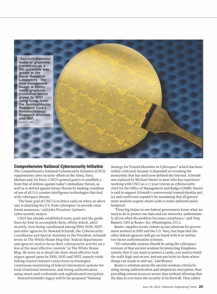
Two-inch-diameterwafer of graphenetransistors on a SiC substrate wasgrown at the Naval ResearchLaboratory. Theblue backgroundimage is honey-comb graphenecrystalline latticegrown by NISTusing funds fromthe SemiconductorResearch Corp’sNanotechnologyResearch Initiativeand NSF.SOURCE: NNI

26 Electronic Engineering Times June 18, 2012
COVER STORY
than punching holes inthe firewall for down-loading data to securelaptops, potentiallyopening a vulnerabilitythat could also allowmalware to beuploaded, Route1'stechnique allowsremote access to securedata without uploadingor downloading–byonly communicatingencrypted screens aftera two-factor smart cardauthentication process.
Smart GridInitiativeThe Smart Grid is nowa three-year old initiative started by President Obama with$3.4 billion in Recovery Act funding which was spent upgrad-ing the U.S. power grid including over $200 million ear-marked for millions of smart meters. Since then a plethora ofnational initiatives have sprung up under the Smart Gridmoniker, most of which you can browse at the DOE website.
Under the Smart Gridrubric is the ModernGrid Initiative (MGI), acollaborative effort ofDOE, the National Ener-gy Technology Laborato-ry (NETL), and manylocal utilities and othercommercial grid stake-holders. Coordinated bythe DOE’s Office of Elec-tricity Delivery andEnergy Reliability, theMGI also coordinateswith other Smart Gridefforts, including Grid2030 (which producedthe National ElectricDelivery TechnologiesRoadmap), GridWise
(which produced the public/private stakeholder consortiumcalled the GridWise Alliance), the GridWorks program(which improves cables, substations and power electronicsincluding high-temperature superconductors), the DOE'sAdvanced Research Projects Agency for Energy (ARPA-E), andthe SRC's Energy Research Initiative.
At Georgia Tech humans train co-robots by example,after which they can help by taking over routinerepetitive tasks. Credit: Thomaz & ChristensenSourcr: Georgia Tech
NASA and GM are collaborating on co-robots that can workalongside people using their same tools.Source: NASA

June 18, 2012 Electronic Engineering Times 27
COVER STORY
"All those U.S. national initiatives are building a solidinfrastructure for a smarter grid–there are a lot of subsidiesfor modernizing the grid and for smart metering," saidBettina Tratz-Ryan, a research vice president at Gartner Inc.(Stamford, Conn.) "What the U.S. needs now, is a nationalgrid policy that everybody agrees on, rather than the frag-mented state-by-state determinations made today. Unfortu-nately, a national policy will be very hard to come by in theU.S., because of the conflicting interests among all thestakeholders."
SRC's Energy Research Initiative (ERI) isaddressing national grid policy. "Making the grid smarter and more robust will help, but thebig payoff will be what we do with those capabilities," said ERIdirector Bob Havemann. "Here at ERI, we believe that what youneed is a detailed model of the entire grid that allows showsthe best way to integrate renewable energy resources, bysimulating different configurations and scenarios."
ERI is funding the effort to create a grid-simulator at themulti-university Smart Grid Research Center at CarnegieMellon University (Pittsburg). SGRC provides modelingsoftware for simulation and control which can manage,optimize and secure a smart power grid. Using dynamicmonitoring and decision systems, the SGRC claims its soft-ware simulator provides a better paradigm for managingelectricity infrastructure.
"Ours is the only center that can simulate the entire grid,including all its resources, and which can show just howgood it can really be," said electrical engineering professorand director of the Center, Marija Ilic.
The Smart Grid Research Center recently demonstratedhow its massive simulator could solve "what if" scenarios by performing a study that demonstrated how an 85 percentgain could be reaped by using smart meters to charge parkedelectric powered fleet vehicles from solar-cells and wind-turbines.
National Robotics InitiativeThe National Robotics Initiative could become a definingproject for President Obama's administration, because if itsucceeds, then American workers will reclaim the lead inmanufacturing over low-paid foreign labor. NRI's roadmapcalls for three milestones–co-worker robots, co-habitat robots,and co-protector robots–each of which is related to multiply-ing the abilities of U.S workers with robotic assistants.
"Co-worker robots are all about empowering regular peo-ple," said Henrik Christensen, the chair of robotics at theGeorgia Institute of Technology (Georgia Tech). "We wantto empower workers, especially in the manufacturing sec-tor, to make them more competitive with low-wage labor-ers in Asia."
Rather than heavy fixed-in-place robots from which assem-bly line workers have to be protected, co-worker robots willbe light-weight and mobile, allowing them to work alongsidehuman workers without the risk of injury.
"Robots today are big and bulky and often kept behind afence, because you are worried about safety," said Chris-
The National Science Foundation (NSF) has been sponsoringongoing national initiatives to chart the wiring diagram andcircuit functions of the neural networks in the brain,discovering scores of new neural circuits every few years,including a recent breakthrough in robotic probes that arecurrently creating a parts-list and wiring diagram for buildingfuture cognitive computers.
Likewise the National Institute of Health is sponsoringmultiple national neural circuitry initiatives that have revealedthe wiring diagramsand functions of manybrain circuits, and insome cases theunderlying algorithmto which they adhere.One recent revelationmade by the NIH'sHuman Connectomeproject, is that brainsappear to be wiredlike the 3-D crossbarswitch that HP isproposing to emulatebrain functions.
The most forwardlooking of theseefforts is the Systemsof NeuromorphicAdaptive PlasticScalable Electronics(SyNAPSE) program atDARPA, which isfunding thedevelopment of brain-like crossbar switchesthat learn usingalgorithms running onneural network cores.IBM, for instance,recently demonstrateda digital neuromorphic microchip, which it calls a cognitivecomputer that can directly emulate its successful softwaresimulations of brain functions.
This breakthrough could be especially important, since theNSF, NIH, NRI and similar efforts have been amassing detailedsoftware simulations of how the brain does its magic. If IBM issuccessful in creating microchips that can execute thesealgorithms in hardware--at speeds even faster than humanbrains--then future mobile devices could acquire learningcapabilities that marry Apple's Siri to IBM's Watson, enablingvoice recognition, natural language understanding andreasoning in a hand-held device. -- R. Colin Johnson
Wiring up neuromorphicelectronics
IBM is mapping out thewiring diagram of thehuman brain which hasover 150 kilometers ofconnections which it issimulating onsupercomputers andemulating withneuromophic cognitivecomputer microchips.

28 Electronic Engineering Times June 18, 2012
COVER STORY
tensen. Co-robots, on the other hand, will help U.S. workersduring manufacturing, but you won't have to worry about acollision with the human, because they will be so lightweightthat the robot will give way to the human if they bumptogether."
The second category, co-habit robots, will perform sur-
gery, aid in rehabilitation and help the elderly age-in-placeat home. And the third category–co-protectors–will assistfirst responders, search disaster sites, perform militaryreconnaissance, and assist firefighters in local neighbor-hoods.
"We envision a range of co-worker robots in each catego-ry, from those that just multiply human abilities, to mobileautonomous models that perform complementary task forhumans," said Christensen. "We believe we can make a realimpact on bringing manufacturing jobs back to the U.S."
Advanced Manufacturing InitiativeThe National Robotics Initiative was announced by Obama asa part of his Advanced Manufacturing Partnership (AMP)headed by MIT President Susan Hockfield and Dow ChemicalCEO Andrew Liveris. AMP aims to reinvigorate manufactur-ing in the U.S. with funding of about $500 million. The NRI isspending about $70 million from that pot in hopes of creat-ing fleets of helper robots to multiply the productivity of U.S.workers.
"NSF will do the basic research, NRI will supply co-robottechnology that multiply U.S. worker's productivity, andNIST will translate those results into standards that get itout of the lab and onto the factory floor," said Christensen.
AMP is housed at NIST where it is managed by Mike Mol-nar, currently the Chief Manufacturing Officer at NIST, butwas the idea of the President's Council of Advisors on Sci-ence and Technology (PCAST). Its charter is to create collab-orative development efforts between industry, academiaand government resulting in emerging technologies, poli-cies and partnerships that reinvigorate advanced manufac-turing in the United States, thus creating jobs.
Besides co-robots that multiply U.S. worker productivity,the Advanced Manufacturing Partnership also aims toincrease the energy efficiency of the manufacturingprocess, invent new materials to speed up the manufactur-ing process, reduce the time needed to make advancedmaterials, invent new methodologies for reducing thelength of the design, build, and test process, and to builddomestic manufacturing capabilities in critical nationalsecurity industries. p
Texas Instruments has been increasing the grain sizeof its chemical vapor deposition (CVD) process formonocrystalline graphene, increasing its originalgrain size from 10 microns to the current worldrecord of 1.5 millimeter shown here on a wavy cop-per surface.Soutce: TI
President Obama announced the national initiativeaimed at revitalizing U.S. manufacturing–theAdvanced Manufacturing Partnership–last year atthe Carnegie-Mellon Robotics Institute’s NationalRobotics Engineering Center.SOURCE: Carnegie Mellon
lRELATED URLS:
Time to play hard ball on tech manufacturinghttp:http://bit.ly/MjBRdX
Obama highlights manufacturing in NY semifab visithttp:http://bit.ly/LuIgY3
U.S. manufacturing effort targets regional clustershttp:http://bit.ly/LBKL9A
Obama's small business guru is chip manhttp://bit.ly/MjClkl
Obama, jobs and the creative destruction of electronicshttp://bit.ly/LEQ4RH

The Newest Products for Your Newest Designs®
ORE.GO
mouser.com
Mouser and Mouser Electronics are registered trademarks of Mouser Electronics, Inc. Other products, logos, and company names mentioned herein, may be trademarks of their respective owners.
mouser.com Distributing semiconductors and electronic components for design engineers.
Authorized Distributor
The widest selection of the newest products.
30 Electronic Engineering Times June 18, 2012
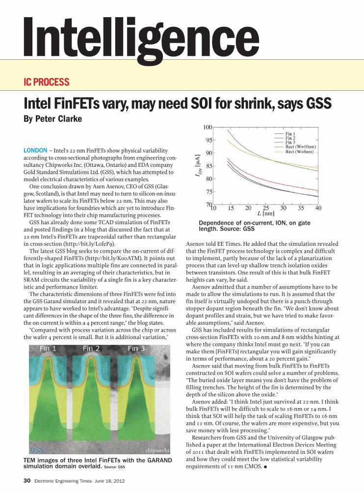
Intelligence
LONDON – Intel's 22-nm FinFETs show physical variabilityaccording to cross-sectional photographs from engineering con-sultancy Chipworks Inc. (Ottawa, Ontario) and EDA companyGold Standard Simulations Ltd. (GSS), which has attempted tomodel electrical characteristics of various examples.
One conclusion drawn by Asen Asenov, CEO of GSS (Glas-gow, Scotland), is that Intel may need to turn to silicon-on-insu-lator wafers to scale its FinFETs below 22-nm. This may alsohave implications for foundries which are yet to introduce Fin-FET technology into their chip manufacturing processes.
GSS has already done some TCAD simulation of FinFETsand posted findings in a blog that discussed the fact that at22-nm Intel's FinFETs are trapezoidal rather than rectangularin cross-section (http://bit.ly/L0feP9).
The latest GSS blog seeks to compare the on-current of dif-ferently-shaped FinFETs (http://bit.ly/Ko0ATM). It points outthat in logic applications multiple fins are connected in paral-lel, resulting in an averaging of their characteristics, but inSRAM circuits the variability of a single fin is a key character-istic and performance limiter.
The characteristic dimensions of three FinFETs were fed intothe GSS Garand simulator and it revealed that at 22-nm, natureappears to have worked to Intel's advantage. "Despite signifi-cant differences in the shape of the three fins, the difference inthe on-current is within a 4 percent range," the blog states.
"Compared with process variation across the chip or acrossthe wafer 4 percent is small. But it is additional variation,"
Asenov told EE Times. He added that the simulation revealedthat the FinFET process technology is complex and difficultto implement, partly because of the lack of a planarizationprocess that can level-up shallow trench isolation oxidesbetween transistors. One result of this is that bulk FinFETheights can vary, he said.
Asenov admitted that a number of assumptions have to bemade to allow the simulations to run. It is assumed that thefin itself is virtually undoped but there is a punch-throughstopper dopant region beneath the fin. "We don't know aboutdopant profiles and strain, but we have tried to make favor-able assumptions," said Asenov.
GSS has included results for simulations of rectangularcross-section FinFETs with 10-nm and 8-nm widths hinting atwhere the company thinks Intel must go next. "If you canmake them [FinFETs] rectangular you will gain significantlyin terms of performance, about a 20 percent gain."
Asenov said that moving from bulk FinFETs to FinFETsconstructed on SOI wafers could solve a number of problems."The buried oxide layer means you don't have the problem offilling trenches. The height of the fin is determined by thedepth of the silicon above the oxide."
Asenov added: "I think Intel just survived at 22-nm. I thinkbulk FinFETs will be difficult to scale to 16-nm or 14-nm. Ithink that SOI will help the task of scaling FinFETs to 16-nmand 11-nm. Of course, the wafers are more expensive, but yousave money with less processing."
Researchers from GSS and the University of Glasgow pub-lished a paper at the International Electron Devices Meetingof 2011 that dealt with FinFETs implemented in SOI wafersand how they could meet the low statistical variabilityrequirements of 11-nm CMOS. p
Intel FinFETs vary, may need SOI for shrink, says GSSIC PROCESS
By Peter Clarke
TEM images of three Intel FinFETs with the GARANDsimulation domain overlaid. Source: GSS
Dependence of on-current, ION, on gatelength. Source: GSS

June 18, 2012 Electronic Engineering Times 31
MALCOLM PENN, CEO of technologyand market analysis company FutureHorizons Ltd., believes in the importanceof retaining control of manufacturingpassionately. He has spoken many timesof the fab-lite business model as beingmerely the reprehensible and drawn-outprocess of abandoning manufacturing.
Penn has also long-warned that aban-doning chip manufacturing in Europewould have consequences in terms ofour ability to create jobs here and to cre-ate value that can be exported. We arestarting to stare those consequences inthe face as countries across Europeteeter on the edge of bankruptcy.
Penn has now had the opportunity toflesh out his thesis in a substantialreport prepared for the European Com-mission. There are indications that atleast some bureaucrats in Brussels arecoming round to Penn's point of view.But that is not enough.
It seems likely that a 450-mm pilot fabbased at IMEC's site in Leuven, Belgiumwill happen. But beyond that, if any ofthe more ambitious plans touched on inthe report are going to happen, they needboth metaphorical and literal buy-infrom the European chip companies.
Last time I took the temperature inEurope on this subject, the EuropeanCommission was a lot more interestedin it than the indigenous Europeancompanies. When it comes to usingEuropean tax payers' money to support450-mm chip manufacturing the Euro-pean chip companies tend to point tomore urgent and near-term things theyneed to spend the taxpayers' money on.
I am sure the EU/EC is aware of a needto reinvigorate European manufacturingand value creation in areas like nanotech-nology and the need to do something toprevent manufacturing continuing todrain east. The European companies tendto just want R&D support for their nearerterm technologies on 300-mm wafers. Idon't see Carlo Bozotti of STMicroelec-tronics, Rick Clemmer of NXP Semicon-ductors or the incoming Reinhard Ploss
at Infineon Technologies changing thatposition any time soon.
And with regard to Penn's idea of a 450-mm fab to giving European companiesan advantage behind the leading-edgethere are yet more hurdles to be over-come.
More-than-Moore technologies for themost part do not require 450-mm diame-ter wafers and in some cases are positive-ly uneconomic on such large wafers. It isnot practical that an entire chip product'slifetime requirement can be produced onjust a few wafers. Indeed there is discus-sion in the MEMS community that 300-mm wafers are still way too large for anydesigns and that 200-mm wafers are onlyjust becoming the sweet spot for con-sumer MEMS with applications thatneed high volumes.
We should remember that Moore'slaw when originally coined was an eco-nomic argument and not a technicalone. The only way I can see 450-mmwafers being used for the smaller vol-umes and wafer area required by manybehind-the-leading-edge technologieswould be if there was a business modelchange so that multiproject wafer runscould become more mainstream, ratherthan a prototyping vehicle.
That could happen but again is prob-ably not a sufficient condition. Thereare arguments regarding amortizationof investments which mean that thenewest, most expensively producedwafers should be used for the largest diewith the highest value per silicon area.Older written-down fabs running small-er wafers have always been used to runolder processes and chips with lowerselling prices.
The best hope I see is that the bureau-crats in Brussels can call in some favorswith the likes of Intel and Global-foundries, who want to be good Euro-pean citizens, to have a leading-edgevolume 450-mm wafer fab be located inDublin or Dresden.
The full report is on the EC’s website(http://bit.ly/KhtCTV).p
Opinion: EuroFab450 is an ambitious dreamCHIP MANUFACTURING
By Peter Clarke
PERFORMANCE,RELIABILITY,ATR SERIES
For more information call 1.800.981.8699or visit www.irf.com
FEATURES
• 30W, single, Dual and Triple Outputs
• Compatible with MIL-STD-704 28V input system
• High power density with small form factor
• MIL-STD-461 compliant with a compatible EMI filter
• Input Voltage: 16V to 40V
• Operates at -55˚C to +125˚C without any de-rating of output power
• Available in DSCC SMD
Dimensions (in.)2.88 x 1.11 x .39
Dimensions (in.)2.11 x 1.11 x .39
THE POWER MANAGEMENT LEADER

Info & Free Samples
Change Batteries in 2018
Features
When You Can’t Afford to Turn it OffEnabling long battery life in an “always-on” system means drawing very little active standby current. Fortunately, our LTC®3104 does just that: its buck regulator can deliver 300mA with up to 95% efficiency with a no load quiescent current of just 1.8µA when in Burst Mode® operation. Its 10mA low noise LDO adds just 1.0µA of quiescent current and can be powered from the buck output. The LTC3104’s wide 2.5V to 15V input voltage range accommodates a variety of input sources, makingit ideal for remote sensor networks, portable instruments and a wide range of battery-powered devices.
• VIN Range: 2.5V to 15V
• VOUT Range: 0.6V to 13.8V
• 300mA Buck IQ = 1.8µA
• 1.2MHz Constant Frequency, Current Mode Architecture
• 10mA LDO IQ = 1.0µA
• LDO Dropout = 150mV
• 3mm x 4mm DFN14, MSE16 Packages
• LTC3103 for 300mA Buck Only in 3mm x 3mm DFN, MSE10
1.8V
1.2V
LTC3104
RUNLDO
RUN
VIN
GND
SW
FB
VLDO
FBLDO
1.2M
600k
600k
600k
IBATTERY = 3.8µA
9V
, LT, LTC, LTM, Linear Technology, the Linear logo and Burst Mode are registered trademarks of Linear Technology Corporation. All other trademarks are the property of their respective owners.
www.linear.com/product/LTC3104
1-800-4-LINEAR
LTC3104 Video Product Brief
Output Current (A)
65
Effic
ienc
y (%
)
95
100
60
55
90
75
85
80
70
0.0001 0.01 0.1 150
0.001
VIN = 4V
VIN = 7V
VOUT = 2.5VL = 10μH
LTC3104 Effi ciency Curve(Automatic Burst Mode Operation)

THE NICHE THAT supercapacitorsserve in the market continues to growin new applications.
Compared to batteries, supercaps pro-vide better power density with higherpeak power delivery capability, smallerform factors, higher charge cycle life overa wider operating temperature range, andlower ESR. Compared to standard ceram-ic, tantalum or electrolytic capacitors,supercaps offer higher energy density ina similar form factor and weight. Asupercap’s lifetime is maximized by
reducing the capacitor’s top-off voltageand avoiding high temperatures (>50°C).Table 1 compares key features.
Early generation 2-cell supercapchargers were designed for low currentcharging from 3.3V, 3xAA, or a Li-Ion/Polymer battery. However, supercaptechnology improvements haveexpanded the market, resulting in aslew of medium to higher currentopportunities not necessarily confinedto the consumer product space.
Primary applications include solid
state disk drives and mass storage back-up systems, high current portable elec-tronic devices such as industrial PDAsand handy terminals, data loggers,instruments, medical equipment, andmiscellaneous “dying gasp” industrialapplications such as security devices,alarm systems and smart power meters.Other consumer applications includethose with high power bursts includingLED flash in cameras, PCMCIA card andGPRS/GSM transceivers, and Hard DiskDrives (HDDs) in portable devices.
DESIGN PRODUCTS+
Supercaps can best batteriesin backup appsBy Steve Knoth
GLOBAL FEATURE
June 18, 2012 Electronic Engineering Times 33

Design challenges for supercapchargersSupercaps have many advantages; how-ever, when used in a stack of two ormore caps in series, they present thedesigner with problems such as cell bal-ancing, cell overvoltage damage whilecharging, excessive current draw and alarge footprint/solution. Higher charg-ing current may be required if frequentbursts of high peak power are needed. Inaddition, many of the charging sourcesmay be current limited, for example, ina battery buffer application or in aUSB/PCCARD environment. Being ableto deal with these conditions is crucialfor space-constrained, higher powerportable electronic devices.
Reverse conduction through an ICtypically results in a catastrophic event.External fixes such as series rectifyingdiodes are not very efficient due to highvoltage drop. Schottky diodes have lessforward drop and therefore higher sys-tem efficiency but are more costly thanregular diodes. On the other hand, fieldeffect transistors (FETs) offer low onresistances and minimal loss. An inter-nal FET-controlling PowerPath circuit isan elegant way to solve the problemthereby eliminating the potentiallydamaging consequences. With Power-Path control, in the event the input sud-denly drops below the output, the IC’scontroller quickly turns the internalFET completely off to prevent anyreverse conduction from the outputback to the input supply.
Cell balancing series-connected super-capacitors ensure that the voltage acrosseach cell is approximately equal; whereasa lack of cell balancing in a supercap maylead to overvoltage damage. For low-cur-rent applications, a charge pump withexternal circuitry with one balancingresistor per cell is an inexpensive solu-tion to the problem; the balancing resis-tor value will depend primarily on thecapacitor leakage currents as explainedbelow. In order to limit the impact of thecurrent drain due to balancing resistorson supercap energy storage, designerscan alternatively use a very low currentactive balance circuit.
Another source of cell mismatch isdifferences in leakage current. Leakagecurrent in the capacitor cells starts offquite high and then decays to lower val-
ues over time. But if the leakage is mis-matched between series cells, the cellsmay become over-voltaged uponrecharge unless the designer selects bal-ance resistors that provide significantlymore load current on each cap than thecap leakage itself. However, balancingresistors burden the application circuitwith unwanted components and per-
manent discharge current. They alsoprovide no overvoltage protection foreach cell if mismatched capacitors arecharged at high currents.
For low to medium power applica-tions, another inexpensive (but compli-cated) approach to solving the supercapcharging problem involves using a cur-rent limited switch plus discretes andexternal passive components. In thisapproach, the current limited switchprovides the charge current and limit-ing, while voltage reference and com-parator ICs provide the voltageclamping, and finally an op amp(sink/source) with balance resistorsenables supercap cell balancing. Never-theless, the lower the ballast resistorvalue, the higher the quiescent currentand the shorter the battery run time;the obvious benefit being saved cost.However, this solution is very cumber-some to implement and performance ismarginal at best.
Any solution to efficiently satisfy thelow to medium current supercap charg-er IC design constraints outlined above
34 Electronic Engineering Times June 18, 2012
DESIGN PRODUCTS+
Figure 1. LTC3226 normal-to-backup mode switching transient waveform
Parameter Supercaps Capacitors Batteries
Energy Storage W-sec of energy W-sec of energy W-Hr of energy
Charge Method Voltage across Voltage across Current & Voltageterminals i.e. terminals i.e.from a battery from a battery
Power Delivered Rapid discharge, rapid discharge, Constant voltagelinear or exponential linear or exponential over long time
voltage decay voltage decay period
Charge/Discharge msec to sec psec to msec 1 to 10 hrsTime
Form Factor small small to large large
Weight 1-2g 1g to 10kg 1g to >10kg
Energy Density 1 to 5Wh/kg 0.01 to 0.05Wh/kg 8 to 600Wh/kg
Power Density High, >4000W/kg High, >5000W/kg Low, 100-3000W/kg
Operating Voltage 2.3V – 2.75V/cell 6V – 800V 1.2V - 4.2V/cell
Lifetime >100k cycles >100k cycles 150 to 1500 cycles
Operating Temp -40 to +85°C -20 to +100°C -20 to +65°C
Table 1. Supercapacitors vs. capacitors vs. batteries


would combine a charge pump-basedcharger for 2 series supercaps withautomatic cell balancing and voltageclamping. Linear Technology has devel-oped a simple, yet sophisticated, mono-lithic supercap charger IC for theseapplications which does not need aninductor, eliminates the need for bal-ance resistors, provides reverse block-ing, has multiple operating modes andalso features low quiescent current.
A simple solutionThe LTC3226 is the newest IC offering inLinear Technology’s family of 2-cellsupercapacitor charger ICs. It has twomodes of operation: normal and backup(Fig. 1). If VIN is above an externally pro-grammable PFI threshold voltage, the
part is in normal mode in which powerflows from VIN to VOUT through theexternal FET and the internal chargepump stays on to top off the superca-pacitor stack. If VIN is below this PFIthreshold, the part is in backup mode. Inthis mode, the internal charge pump isturned off, the external FET is turned offand the LDO is turned on to supply theload current from the stored charge.
The LTC3226 offers a number of use-ful features in a small footprint, reduc-ing overall solution size and in turnenabling more compact, simplerdesigns. Table 2 shows a comparison ofLinear Technology’s family of superca-pacitor chargers.p
36 Electronic Engineering Times June 18, 2012
DESIGN PRODUCTS+
l MORE online at http://bit.ly/L3QUvz
Steve Knoth is a SeniorProduct Marketing Engineerin Linear Technology’s PowerProducts group. Prior to
Linear Technology he held variousmarketing and product engineeringpositions at Micro Power Systems, AnalogDevices and Micrel Semiconductor.Knoth earned a BS in ElectricalEngineering and a Master’s degree inPhysics from San Jose State University,and an MBA in Technology Managementfrom the University of Phoenix.
Manufacturer Linear Tech Linear Tech Linear Tech Linear TechPat number LTC3226 LTC3225/-1 LTC4425 LTC3625/-1
SCAP charging 1x/2x charge pump 1x/2x charge pump Linear charger buck (from Vin)/Topology +LDO w/50mohm boost (from Vmid)
ideal diode regulator(inductor-based)
Max charge current 150mA 150mA 2A continuous, 1A (2 inductor),(315
SCap cell voltage Yes Yes Yes Yesregulation/limiting/OVP
Max SCap Value unlimited unlimited unlimited unlimited
Auto cell balancing Yes Yes Yes Yes(also while charging) (also while charging) (also while charging)
PowerPath control Yes No No No
External Vin to Vout Yes No No No
Input voltage range 2.5V to 5.5V 2.8Vto 5.5V 2.7V to 5.5V 2.7V to 5.5V
Quiescent current Iq 55µA 20µA 20µA 23µA
Protection Current limit, Current limit, Current limit, Current limit,thermal limit, thermal limit, thermal limit, thermal shutdown,
reverse current reverse current theraml SD, reverse currentreverse current
Package(s) 3x3 QFN-16 2x3 DFN-10 3x3 DFN-12, 3x4 DFN-12MSOP-12
Table 2. Comparison of Linear Technology supercap charger ICs

The most advanced search engine for
CompareElectronic Parts
Get Pricing &Inventory
Discover NewElectronic Parts
NEW
ParametricallySearch Parts
Electronic Engineers & Buyers. For free.

38 Electronic Engineering Times June 18, 2012
DESIGN PRODUCTS+
AS AUDIO INTEGRATED-CIRCUIT (IC) designs move to fin-er geometries, it becomes more difficult to design, and lesscost-effective to integrate, high-performance analog circuitson the same piece of silicon with high-density digital circuits.Audio system architects are pushing analog portions of anaudio signal chain further towards the input and outputtransducers and connecting everything in between digitally.
As the analog circuits are pushed to the edges of the signalchain, digital interfaces between ICs in the chain becomemore prevalent. DSPs have always had digital connections,but now digital interfaces are being included on the transduc-ers and amplifiers that usually have had only analog inter-faces. A traditional audio signal chain may have analog signalconnections between microphones, preamps, ADCs, DACs,output amplifiers, and speakers, as shown in Figure 1.
IC designers are integrating the ADCs, DACs, and modula-tors in the transducers on opposite ends of the signal chain,which eliminates the need to route any analog audio signalson the PCB, as well as reduces the number of devices in thesignal chain. Figure 2 shows an example of a completely-digi-tal audio-signal chain.
There are many different standards for transmitting digital-audio data from one place to another. Some formats, such asI2S, TDM, and PDM are typically used for inter-IC communi-cation on the same PC board. Others, such as S/PDIF and Eth-ernet AVB are primarily used for data connections from onePCB to another through cabling.
This article will focus on the differences, advantages, anddisadvantages of the inter-IC, rather than inter-board, digitalaudio formats. Choosing audio components with mis-matched digital interfaces needlessly complicates the systemdesign; understanding the pros and cons of different inter-faces before selecting parts helps to streamline your compo-nent selection and ensure that you have the most-efficientimplementation of the signal chain.
Inter-IC Sound (more commonly called “I-squared-S” or“I-two-S”) is the most common digital audio format used foraudio data transfer between ICs. The I2S standard was intro-duced by Philips Semiconductors (now NXP) in 1986 and wasrevised in 1996. The interface was first popularly used in CD-player designs, and now can be found in almost any applica-tion where digital-audio data is being transferred from one ICto another. Most audio ADCs, DACs, DSPs, sample-rate con-verters, and some microcontrollers include I2S interfaces.
An I2S bus uses three signal lines for data transfer – aframe clock, a bit clock, and a data line. The two clocks can begenerated by the receiving IC, the transmitting IC, or even aseparate clock-master IC, depending on the system architec-ture, Figure 3. An IC with an I2S port can often be set to be ineither master or slave mode. Unless a sample-rate converter isbeing used in the signal chain, a system will usually have asingle I2S master device so that there are no issues with datasynchronization.
The Philips standard for these signals uses the names WSfor word select, SCK for the clock, and SD for the data,although IC manufacturers seem to rarely use these names intheir IC datasheets. Word select is also commonly calledLRCLK, for “left/right clock”, and SCK may be called BCLK,for “bit clock” or SCLK for “serial clock”.
The name of an IC’s serial data pin varies most from one ICvendor to another, and even within a single vendor’s differentproducts. A quick survey of audio IC datasheet shows that theSD signal may also be called SDATA, SDIN, SDOUT, DACDAT,ADCDAT, or other variations on these, depending on whetherthe data pin is an input or output.
An I2S data stream can carry one or two channels of datawith a typical bit clock rate between 512 kHz, for an 8-kHzsampling rate, and 12.288 MHz, for a 192-kHz sampling rate.The data word length is often 16, 24, or 32 bits. For wordlengths less than 32 bits, the frame length is often still 64 bits
Common Inter-IC digital interfacesfor audio data transfer
PLANET ANALOG
By Jerad Lewis
Figure 1: Traditional audio signal chain

and the unused bits are just driven low by the transmitting IC. Although it is rare, some ICs only support I2S interfaces
with a maximum of 32 or 48 bit clocks per stereo audio frame.A system designer has to be careful when using one of theseICs to make sure that the devices on the other end of its con-nections can also support these bit clock rates.
While I2S format is the most commonly used, there are oth-er variants of this same three-wire configuration, such as left-justified, right-justified, and PCM modes. These differ from I2Sby the position of the data word in the frame, the polarity ofthe clocks, or the number of bit clock cycles in each frame.
TDM formats Some ICs support multiple I2S data inputs oroutputs using a common clock, but this obviously increasesthe number of pins necessary to transfer the data. Time divi-sion multiplexed (TDM) formats are used when more than twochannels of data are to be transferred on a single data line. ATDM data stream can carry as many as sixteen channels of dataand has a data/clock configuration similar to that of I2S.
Each channel of data uses a slot on the data bus that is 1/Nth
the width of the frame, where N is thenumber of channels being transferred. Forpractical purposes, N is usually roundedup to the nearest power-of-two (2, 4, 8, or16) and any additional channels are leftempty. A TDM frame clock is often imple-mented as a single bit-wide pulse, ratherthan I2S’s 50% duty-cycle clock. Clockrates above 25 MHz are not commonlyused for TDM data, since higher frequen-cies cause board layout issues that PCB
designers would rather avoid. TDM is commonly used for a system with multiple
sources feeding one input, or one source driving multi-ple devices. In the former case, each TDM sourceshares a common data bus. The source must be config-ured to drive the bus only during its appropriate chan-nel, and tri-state its driver while the other devices aredriving the other channels.
There is no standard for TDM interfaces, such as thePhilips standard for I2S. This means that many ICshave their own slightly-different flavor of a TDM
implementation. These differences may includeclock polarities, channel configuration, and tri-stat-ing or driving unused channels. Of course, these dif-ferent ICs will usually work together, but a systemdesigner needs to take care to ensure that outputs ofone device will spit out data in the format that theinputs of another are expecting!
PDM data connections are becoming more com-mon in portable audio applications, such as cellphones and tablet computers. This is an advantagein these size-constrained applications because PDMaudio signals can be routed around noisy circuitry,such as LCD screens, without having to deal withinterference issues analog audio signals might have.
With PDM, up to two audio channels can betransmitted with only two signal lines. Figure 4shows a system diagram with two PDM sourcesdriving a common data line into a receiver. A clock
generated by the system master can be used by two slavedevices, which use alternate edges of the clock to output theirdata on a common signal line.
The data is modulated at a 64x rate, resulting in a clockthat is typically between 1.0 and 3.2 MHz. The bandwidth ofthe audio signal increases as the clock rate increases, so lowerfrequency clocks are used in systems where a reduced band-width can be traded off for lower power consumption.
A PDM-based architecture differs from I2S and TDM in thatthe decimation filter is in the receiving IC, rather than thetransmitting IC. The output of the source is the raw high-sample-rate modulated data, such as the output of a Sigma-Delta modulator, rather than a decimated data, as it is in I2S.A PDM-based architecture reduces the complexity in thesource device, and often makes use of decimation filters thatare already present in a codec’s ADCs.
This allows system designers to not only use audio codecsthat they may already be using, but also take advantage of adigital data connection’s reduced sensitivity to interference.
June 18, 2012 Electronic Engineering Times 39
DESIGN PRODUCTS+
Figure 2: Fully-digital audio signal chain
Figure 3: I2S connection diagram, receiver as master
Figure 4: Dual-source PDM connection diagram
Haptic response embedded in flat panelsHiWave Technologies has launched a touchfeedback platform for control panels to beintegrated in everyday household appli-ances.
The Taptic demonstration platform usesHiWave third dimension haptics. It incorpo-rates two HiWave HIHXC9C005-8 hapticactuators, which attach to the back of a flatprinted touch interface panel, and a HiWaveHiHS9002 haptic control integrated circuit.It can work with both capacitive and resis-tive touch panel technologies.
The key benefit of HiWave's patentedBending Wave Haptics is that the panel canbe firmly fixed, or integral in the appliance.No physical movement is necessary asBending Waves creates the tactile sensationlocally in the touch panel.
HiWave's algorithms processed in thecompany‘s haptic control chip enables hap-tic feedback responses to be preciselyselected and tuned by both the user andmanufacturer to replicate a wide range ofbutton press sensations. The frequency ofoperation delivers over an octave for truewideband haptics, and up to 15-kHz foraudio playback. A range of audio feedbacks– from simple pings and clicks to MP3 filescontaining spoken instructions and music -can also be delivered without additionalspeakers by using the touch panel as thesound emitter.
HiWave's Taptics reference platform isavailable for demonstration and evaluationunits will be available during 2Q12. TheHiHS9002 control IC and HIHX9C005-8 hap-tic exciters are also available immediately,in high volume quantities, from HiWave andits distributors. Full story: http://bit.ly/Mte4aXwww.hiwave.com
Transceiver matches potential of Super-Speed USB 3.0 specTI’s TUSB1310 provides essential physical-level functions and features sensitivity twicethe USB 3.0 requirement. USB has come along way from its initial 12 Mb/s rate androle as a basic, standardized interfacebetween PCs and peripherals such as key-board, mouse, or scanner.
The SuperSpeed 3.0 specification
intends to achieve a transfer speeds of 5.0Gbit/s with raw throughput of 4 Gbit/s, andit is possible and reasonable to achieve 3.2Gbit/s (0.4 GByte/s or 400 MByte/s), andpossibly more, after protocol overhead.
The performance attributes include: adifferential peak-signal receiver sensitivityof 50 mV; IC can use the system clock as asource. The TUSB1310 can also implementspread-spectrum clocking from the systemclock, thus cutting the BOM size and costwhile reducing EMI.
The TUSB1310 is packaged in a 175BGA and starts at $6.00 in 1,000-unitquantities; it is available now. Full story: http://bit.ly/KPqBe6www.ti.com
Crimp-style connectors offer design flexibilityJST Corp. developed the PNI series of crimp-style connectors that offer both wire-to-board and wire-to-wire applications on a2mm (0.79”) pitch.
The PNI series incorporates either wire-to-wire or wire-to-board connections withoutswitching to a different connector series.The through-hole headers and housingsincorporate both polarization and secure,positive locking. The positive locking incor-porates an inertia lock feature designed toprevent incomplete mating of the connectorhalves.
The PNI Series is suitable for high vibra-tion applications. Optional secondary retain-ers ensure the contacts are fully seated andlocked into the housings to prevent anychance of contact back-out.
The PNI single row, crimp style connec-tor series is available in two through 10 circuits and is rated at 3.0 A (AC/DC) usinga 22 AWG wire at 100 V AC/DC. Wire sizesrange from AWG # 28 to 22. Temperaturerange is -250C to +850C, including temper-ature rise in applying electrical current. Contacts are offered on standard size reelsfor semi-automatic or fully automatic application tooling. Full story: http://bit.ly/KhnEUbwww.jst.com
40 Electronic Engineering Times June 18, 2012
DESIGN PRODUCTS+
EETimes.com Products:
Focus on InterconnectsAlso, these decimation filters may bemore efficiently implemented in thefiner silicon geometries used for fabri-cating a codec or processor, rather thanwhat is used on the microphone ICs.
Codecs, DSPs, and amplifiers havehad I2S ports for years, but until now asystem’s input devices, such as micro-phones, have had either analog or PDMoutputs. As the digital interfaces arepushed further towards the ends of thesignal chain, new ICs will be needed tosupport these new system architectures.
Microphones that have an integratedI2S interface, such as the AnalogDevices ADMP441 MEMS microphone,make it easier for designers to build thiscomponent into systems where PDMmicrophones are not easily used orwhere analog interfaces are not desired.Only a subset of audio codecs accepts aPDM input and very few audio proces-sors outside of those specificallydesigned for mobile phones and tabletsnatively accept this type of data stream.
In some designs, an I2S output micro-phone could completely eliminate theneed for any analog front-end circuits,since many designs may only have anADC and PGA in order to support amicrophone input to the processor. Anexample of a system like this is a wire-less microphone with a digital transmit-ter. The wireless transmitter SOC maynot have a built-in ADC, so using an I2Soutput microphone enables the connec-tions between the transducer and trans-mitter to be completely-digital.
I2S, TDM, and PDM audio interfaceseach have their advantages and applica-tions for which they are best-suited. Asmore audio ICs are transitioning fromanalog to digital interfaces, systemdesigners and architects will need tounderstand which of these interfaceswill be most appropriate for their par-ticular design. With a digital signalchain from microphone to DSP toamplifier, analog signals can be pushedcompletely off of the PCB and exist onlyin the acoustic domain.p
Jerad Lewis is an applications engineer forMEMS microphones at Analog Devices. Hejoined the company in 2001 after gettinghis BSEE from Penn State University. Sincethen, he’s supported different audio ICs,such as converters, SigmaDSPs, and MEMSmicrophones.

Ruggedized keyboards are Atex-approved Computing in potentially explosive environ-ments is now safer and more user-friendlywith the addition of an Atex-certified line ofexternal keyboards into the marketplace.iKey has announced its DT-102-EX family ofproducts, which is approved for use in avariety of classified hazardous locations.
The DT-102-EX line features fully sealed,Nema 4X keyboards constructed with stain-less steel enclosures and keycaps makingthem virtually indestructible, tamper proof,and corrosion resistant. The DT-102 EXproducts are engineered to withstand theharshest of environments, including thosefound in offshore drilling and well pumpingapplications. This line is low-maintenance,easy to clean, and also includes an integrat-ed touchpad, making it a complete, user-friendly solution.
The DT-102-EX line is available in a vari-ety of cable configurations. Installed with aproperly-rated isolation barrier, the key-boards can be ordered in PS/2, PS/2 withbulkhead connectors, or USB connectors.Full story: http://bit.ly/K6lbdUwww.iKey.com
In-cell device integrates touch and display driver Synaptics Inc. announced the first productin its ClearPad Series 4 integrated capaci-tive touch and display driver IC (TDDI) solu-tion family, the ClearPad 4260. The In-Cellready ClearPad 4260 supports WVGA reso-lution LCD low-temperature polysilicon(LTPS) displays up to 5 inches and is tenfinger multi-touch capable. LeveragingSynaptics' industry leading In-Cell touch dis-play technology, the ClearPad 4260 revolu-tionizes mobile capacitive touch solutionswith a single chip, mobile touch and displaydriver IC, all targeted at the fast growingglobal smartphone market.
The ClearPad 4260's innovative touchand display driver integration (TDDI) archi-tecture delivers unprecedented systemadvantages over traditional discrete touchand display driver implementations. TheClearPad 4260 combines Synaptics' indus-try leading performance multi-touch tech-nology with the display driver (DDI) into asingle chip solution that delivers improvedsystem latency with the most advanced dis-play noise management and best-in-classcapacitive sensing performance. Synaptics'touch and display integration (TDDI) solu-tion also enables In-Cell technology whichprovides a cost effective solution with a thin
form factor by eliminating the discrete sen-sor resulting in improved display brightnessand lower power consumption. This integrat-ed solution reduces supply chain complexityby reducing the number of components andeliminating the discrete sensor.
Synaptics is working with leading displaycompanies to serve major OEMs worldwide.The ClearPad 4260 will be available formass production in Q3 2012. Full story: http://bit.ly/NY1t2Qwww.synaptics.com
Data bus coupler is MIL-STD-1553 readyBeta Transformer Technology Corp., a sub-sidiary of Data Device Corp., has launchedthe BXC-A-3, MIL-STD-1553 data bus cou-plers designed for use in systems develop-ment, benchtop test and flight maintenanceapplications.
The coupler delivers high-reliability andoptimum MIL-STD-1553 data bus perform-ance in a miniature footprint by utilizingBeta’s compact and field proven MIL-PRF-21038 transformers. The BXC-A-3 operatesover the full military temperature range of -55°C to +130°C.
Data bus interconnect accessories arealso available.Full story: http://bit.ly/LKaf2Nwww.bttc-beta.com
MEMS accelerometer uses smallest powerAnalog Devices Inc. has started to sample aMEMS accelerometer that it claims deliversthe industry's lowest power.
According to ADI, the ADXL362, 3-axis,digital MEMS accelerometer operates at300 nanoA in motion sensing wake-upmode, consuming 60 percent less currentthan the closest competing sensor in thesame mode. In full measurement mode, theADXL362 uses 2 microA at a 100 Hz datarate, using 80 percent less power than competing MEMS accelerometers operatingat the same frequency, ADI added.
This low power consumption allows theADXL362 to be used in applications thatrequire battery life expectancy of months or years, and where battery replacementcan be impractical or dangerous to theequipment or operator.
Pricing starts at $3.97 each in 1K quantities; sampling now with full produc-tion planned for August 2012.Full story: http://bit.ly/MSRxuRwww.analog.com
IP67-sealed tactile switch is for smartmeteringC&K Components has developed the KSEseries, a low-profile tactile switch that isclaimed to combine rugged IP67-rated seal-ing, reliability and a long-operating life. It issuitable for price sensitive applications,including smart meters, smoke and firedetectors as well as carbon monoxidedetectors.
The single pole single throw (SPST) KSESeries features mechanical parametersbased on a force of 1.5 ± 0.5N, tactile trav-el of 0.3 +0.1/-0.2mm, and an operationallife of 300,000 cycles. More info: http://bit.ly/LEs9Hqwww.ck-components.com
Tact switch offers LED illumination,surface mount designE-Switch launched its TL3240 seriesilluminated tact switch, which is a surfacemount device that offers LED illuminationin blue, red, green and yellow. Cap options are offered, but are orderedand shipped separately. The caps cannotgo through the reflow soldering process.Cap color choices include black, red, blue,ivory, green and yellow, and are offered in asquare or rectangle shape.
The TL3240 series tact switch comesin tape and reel packaging at 500 piecesper reel.
Applications and markets that couldreadily use this illuminated tact switchinclude the audio/visual market, computerperipherals, consumer electronics, instrumentation, telecommunications, and medical equipment, among others.
Key highlights include: • Life Expectancy: 200,000 cycles • Contact Rating: 50mA @ 12V DC • Contact Resistance: 100mΩ Max • Insulation Resistance: 100 MΩ min
at 500V DC • Dielectric Strength: 250V AC for 1 min. • Operating Temperature: -25°C to 70°C • Operating Force: 100gf ± 50gf; 160gf
± 50gf; 260gf ± 50gf • Travel: 0.2mm ± 0.1mm • Contact Arrangement: SPST, normally
open More info: http://bit.ly/KooNtjwww.e-switch.com
June 18, 2012 Electronic Engineering Times 41
DESIGN PRODUCTS+

PRODUCT OF THE TIMESAll New SMART TWEEZERS ST-5LCR Meter for Surface Mount Technology Hand-held device with bench-type accuracy
Toll Free: 1-877-823-7576Fax: 1-519-725-9522
www.siborg.com
To recieve 17% off, visitsmarttweezers.ca/saleSALE
www.vpirf.comTel: (801) [email protected]
engineering
DESIGN ENGINEERING& CONSULTING
We can fix your tough RF problems!
rece
iver
s - t
rans
mitt
ers
- syn
thes
izer
s - m
odul
ator
s - a
nten
nas
RF, Microwave, Mixed Signal
CLASSIFIEDS
42 Electronic Engineering Times June 18, 2012
Senior Manager, RF Packaging: Required by RF Micro Devices, Inc.Position in Greensboro, NC. Directs development of new package require-ments and oversees the quality of existing packages for all product groups.Will oversee the coordination of activities at internal and contract packagingassembly and labeling sites, package design to ensure proper compliance,reliability, product identification, consumer appeal, printing appearance, andproduction techniques. Requires current knowledge of RoHS requirementand applications. Selects, develops, and evaluates personnel to ensure theefficient operation of the function. Assures planning milestone completionfor developmental products, including sample deliveries through initial pro-duction deliveries. Provide guidance to the Design Engineer groups with thepackaging design and manufacturing aspects of the RF product designs.Interface with RFMD customers on Packaging technology. Provide assemblydrawings, material sets, process requirements and other manufacturing docu-mentations. Create and maintain the accuracy of the packaging documenta-tion of each product: list of applicable specifications and assembly draw-ings. Lead assembly process development projects internally and with thehelp of subcontractors. Responsible for ensuring the production scheduleand the production commitments can be met. Meet the operation targets:yield, output, cost and cycle time process. Support the ramp-up of produc-tion volumes with the subcontractors and their supply base. Developsdesigns to meet requirements needed for the nature of the product, trans-portation methods, cost considerations, legal requirements, and packagecontent characteristics. Considers the need for resistance to external vari-ables such as temperature variations, light, moisture, and corrosive chemi-cals. Require MS in Manufacturing Technology (or foreign equivalent) andfive years experience in packaging and packaging management, preferablyin the high-tech industry. 40 hours a week, 8 a.m. 5 p.m. Qualified candi-dates send resumes to [email protected] and reference Job CodeJLDRY.
Senior Software Engineer,Alpharetta GA: Analyze, design,develop, test, manage & upgradeOracle Enterprise ResourcePlanning Software Applications &Databases. Exp in integrationOracle & Metrix/BPCS apps, usingOAF, XML, PLSQL & BizTalk.Some travel, Req's M.S./M.A. in Comp.Sci/Engineer/Business & 9mos exp in Job Offered, orB.S./B.A. & 5 yrs post Bach. exp including. 12 mo. in job offered.Reqs. PMP cert. Send resume toPolaris Associates Inc, 11800 Amber Park Dr., Ste 300,Alpharetta GA 30009

June 18, 2012 Electronic Engineering Times 43
EE LIFE
Most engineers are lazy…and that's often a good thing
ENGINEERINGPOP CULTURE
LAZY PEOPLE CAN also be the mosteffective and productive, it seems to me.[OK, calm down, there's no need to getangry at me, at least not yet.]
Here's what I mean: "lazy" is not thesame as "sloth". When you are slothful,your preferred activity is to sit arounddoing nothing or very little, and avoidwork. That's not engineers.
But when you are lazy, you look to dothings in the most effi-cient way possible, so youdon’t have to re-do them,or so you have time forother things. In this sense,being lazy is just a comple-ment to being efficientand productive—but with-out all the "running-around, looking-busy"mode we often see.
Yes, some of that hustleand bustle is someone getting a lotdone, but often, they are trying to playcatch-up due to poor planning or inef-fective execution of the task.
But a lazy engineer: • looks at what has to be done, thentries to figure out what tools, tech-niques, setups, fixtures, and jigs willallow the overall project to be donebetter and faster—even if it meanstaking time up front to plan or cre-ate these items.
• understands that such a modest ini-tial investment in the above itemscan pay big benefits later on viasmoother project development, bet-ter documentation, or fewer mis-takes and re-spins.
• is often (not always) organized, so asnot to waste time looking for a file,
note, component, or other items.The problem is that management
often mistakes such laziness for out-right slothfulness. I did so, too, once,until I got smarter.
Here's why: Back when the Earth wasstill flat and microprocessors were juststarting to rule the land, our four-per-son product development team (two ofus for circuits, one for software, one for
system integration) alsohad an assigned techni-cian. This fellow neverlooked like he was doinganything. He movedslowly, deliberately, andmethodically. At onepoint, managementasked us if he actuallydid much of anything.
Reality was that hewas extremely efficient
and cool under pressure, and we couldnever keep up with him. We'd givehim a set of tasks, and he'd go off andmake list of what he needed, get them,pull things together, and then do them.(Ken V: if you are reading this, it's you.)He also knew everyone in the shoparea, and so could get things likerough-cut prototype RF shields madeon the side, without formal paper-work.
So, hail to the laziness of engineers, Isay. But don’t worry, I won’t be tellingthe general public that good engineersare also lazy—they would very likelymisinterpret my point.
Have you ever had a similarencounter with lazy-looking engineerswho were also very efficient? Or hadcases where the outward appearance ofa member of your team was actuallyvery different from their actual contri-bution, like our technician?
By Bill Schweber
l JOIN THE CONVERSATION:
http://bit.ly/K0t7xk
(And you can get angry at me now, ifyou still want to.) p
READERS WEIGH IN: If this is the new lazy, then I want to be lazy.This is kind of like a zen guy. One thatknows that planning is very important. Thisreminds me of Stephen Covey, the author ofSeven Habits of Highly Effective People. Hesays that everything is created twice, onewhen planned and the 2nd time when exe-cuted. An efficient person may seem lazyfrom the outside but the thing is that manythat seem hyper-active are really with pend-ing items. This kind of lazy requires a verywell organized mind. This lazy is good. Seekthy lazy state if you will. -- Luis Sanchez
Engineers got to be quick and clever. Anywork done urgently will give lot of errorsresulting in losses. But if we know the workfully we should do it fast and finish as quickas possible .If it is a new work then plan-ning takes time to reach the goals. -- agk
At my first job out of school I did a lot ofsoldering. If I was working on a board Iwould put it in a board vise. A chassis Iwould stand on end. Then lean back in mychair, feet up on the little shelf under thebench and solder away. The president of thecompany said I looked too comfortable andit didn't look good when customers walkedthrough. -- FrankCF
One can be "too lazy" to the point whereyou spend all day automating a half daytask. Mind you the problem either goesaway 'cause you took too long, or comesback anyway and you get a three quarterday rest each time ;-) – philipoakleyThe expression "work smart" as opposed to"work hard" suggests some laziness ishealthy. -- resistion
Although we could pick a more complimen-tary word, lazy gets people's attention andit is what they think we are when we arebeing efficient. This type of "laziness" isalso what one of my professor's said was aprerequisite for a good engineer. – ccidarth

44 Electronic Engineering Times June 18, 2012
EE LIFE
DRIVE FORINNOVATION
The zero-sum renewable energy argument
IN A WAY, the Internet's proximity and ease of use is a shame; itenables complex situations to be oversimplified, which, in the longrun, can hurt public policy making.
There's no better example than renewable energy, which is thesupposed salve for our fossil-fuel problem. Now, solar power isbeing specifically touted as a way to power the cloud's huge, energy-slurping data centers.
Amazon web services engineerand vice president James Hamiltontouches on the challenge in a recentpost (go to the url below and scrolldown to the headline "I love solarpower but…").
In short, Hamilton says the num-bers and the real estate don't add up.
For example, he notes that Apple'snew data center in Maiden, N.C., getssome of its massive energy require-ments (estimated at 78 MW to 100MW) from a solar array that occu-pies 171 acres or (7.4 million squarefeet). To build a solar facility to meetall of the data center's needs wouldrequire the plant to be 24.4 timeslarger than the center itself!
Robert Bryce, writing in the WallStreet Journal, cites these numbers aswell as ardent calls from environmentalgroups for a "clean cloud."
My question is, if we accept reason-able trade-offs in our engineering labs(and our consumer electronics purchas-es!), why can't we accept reasonabletrade-offs in the public conversationover renewable energy usage?
Why can't we just agree that renew-able energy has a small and growingrole in serving our energy appetite butit won't, at this point in history, solve allour needs? p
READERS WEIGH IN: Shoot…. who’s going to publish an article
about people being reasonable?? Thatwould be like watching a reality show aboutnormal people living a normal life… there’sjust no audience for it.
Clearly, there’s a finite supply of cheapfossil fuel. Until its cost rises to the pointwhere renewable energy is competitive, it’sonly going to attract those who place a valueon its green attributes, and not those whojust want to buy energy from a genericsource.
Personally, I value renewables because
By Brian Fuller
I’m aware of how much coal is locallyburned to generate electricity and howmuch mercury and toxins it deposits locally.The issues with CO2 generation are anotherfactor for my preference to reduce fossilfuel use. I’m in favor of research intorenewable fuels because I know how muchlife would change without them after weneed/have to stop using them.
Any idea what the point was for theremark about the solar power facilitybeing bigger than the data center? Howis that an argument against renewables?Maybe it’s really an argument for coveringparking lots with overhead solar panels?
-- Steve Kurt
The point about the size of the array torun the center was that while somethings can be done, it would be dumb todo them. For data centers I have suggest-ed just circulating ambient air through,instead of using refrigeration systems,and don’t make them so tightly packed,so that they can cool better. What we aregoing to find is that we will need todevelop a process that converts wasteinto fuel much more rapidly than the wayit happened last time, in nature. Using
solar energy to rip apart the molecules intosmaller molecules that can work as fuel isthe basic concept, the challenge is thatnobody has figured out how to do it eco-nomically yet. We already can see thatwaste in landfills produces methane enoughto cause problems, so perhaps there is away to have giant “digesters” work on ourgarbage and produce methane much faster.Methane is not the best fuel but we canproduce it without much effort, so far. Asimilar process produces methane gas inour sewer systems if we don’t prevent it.So there is one way that would not need anew breakthrough. -- William Ketel
Renewable energywon't, at this point inhistory, solve all ourneeds
l JOIN THE CONVERSATION:
http://bit.ly/NNogOS

Of course eating less is not enoughon its own; it’s also important to exer-cise. I used to walk every day a fewyears ago, but I fell out of the habit(you miss one day, then another, thenyou find a week’s gone by, then amonth…). Well, that’s all over – I’mgoing to start walkingagain. The thing is that Ilike to have a goal to aimat, so I’ve decided to walkfrom Central Park in NewYork to Fisherman’sWharf in San Francisco.
Actually, much as Iwould like to, I’m notactually going to walk thepath, because I have a wife and sonwho would miss me and I have a jobthat won’t do itself. Instead, I’m goingto keep track of how far I walk andthen plot my virtual progress on themap. I started off by asking Google fordirections from Central Park to SanFrancisco. The result three pages ofdirections, and a summary that said
the total distance was2,911 miles.
When I glanced at thedirections for exitingCentral Park theyseemed a little strange,so I zoomed in on the map to see what
was happening. These direc-tions had me starting off byheading North-North-East,then doing a U-turn, thencoming back through Cen-tral Park, followed by a little“jig”, then under the LincolnTunnel, followed by a 360-degree loop.
The problem, of course,was that I had asked for driving direc-tions. When I clicked the button for walking directions, things changedslightly. Now the journey has grown to2,966 miles (with 49 pages of direc-tions) and early on I have to take ashort excursion into Canada (I hopethey will be kind to me).
I’m not in any rush here, you
IN MY EARLIER column I mentioned that I had juststarted reading A. J. Jacobs’ latest work – Drop DeadHealthy – One Man's Humble Quest for Bodily Perfec-tion.
Well, I finished this book yesterday, and let me start bysaying it was a jolly good read. It is particularly interest-ing to me because I really do need to change my ownlifestyle – spending eight hours a day working on a com-puter without taking any form of break or exercise is notdoing me any good at all. This isn’t just about losingweight and getting “6-pack abs” (although that would benice), it’s also about increasing one’s lifespan, freedomfrom disease and pain, and achieving a sense of emotion-al, mental, and physical well-being.
June 18, 2012 Electronic Engineering Times 45
EE LIFE
I’m going to walk across America!
ENGINEERS’BOOKSHELF
By Clive Maxfield
l JOIN THE CONVERSATION:
http://bit.ly/JSjgVB
Get more suggestions for your summerreading list: http://bit.ly/LeGZST
understand. As part ofits directions, Googleinforms me that my trekis anticipated to take 39days and 4 hours, butthat assumes I’m doingnothing but walking allday, every day. In reality,I’m only going to walk a little here and a littlethere when I can, so itcould take me two orthree years to completemy journey. I don’t care… I have my goal … as theChinese philosopherLao-tzu (604 BC - 531BC) famously said: “A
journey of a thousandmiles begins with a sin-gle step.”
Last but not least, youwill be happy to knowthat I’m not going tobore you with this on aday-by-day basis. I’m justgoing to quietly go off
and do my own thing. Having saidthis, once I start seeing some signifi-cant progress, it’s hard to imagine thatI won’t be shouting it from therooftops.
In the meantime, do you have anytips and tricks on how to lose weight(and keep it off) and generally increaseone's health and well-being?p
I’ve decidedto walk fromCentral Parkin New Yorkto Fisherman’sWharf in SanFrancisco

46 Electronic Engineering Times June 18, 2012
LAST WORD
The panel said it's time to movebeyond standalone intellectual proper-ty blocks to IP subsys-tems—larger chunksof IP that have beenstitched together frommany smaller blocksand pre-verified toensure performanceand compatibility.
"I think we areabout a year year-and-a-half away from sucha marketplace," Sher-wani said. He hintedthat Open-Siliconmight get the ballrolling on such anendeavor in a forth-coming announce-ment. The initiative,he said, had to be tak-en by design service companies or oth-er neutral parties as opposed to the IPvendors themselves, which have novested interest in facilitating access tocompetitors' products.
Sherwani said he realizes that theprospect of such a marketplace facesmany challenges, but that they aresolvable and could be overcome in twoto three years. He also said a robustmarketplace would not come to
fruition overnight, but that the jour-ney needed to begin with a single step,
even if it initially includedonly a fraction of the IPavailable in the market.
While not discountingthe possibility of such amarketplace, other panelmembers cautioned that theprocess of selecting andimplementing IP could onlybe automated to a degree.Verifying that a piece of IPwill work as expected in aparticular design will con-tinue to be a challenge, theysuggested.
Under Sherwani's propos-al, the IP marketplace wouldinclude all relevant informa-tion and up-to-datedatasheets for IP blocks and
subsystems to enable designers to selectand purchase IP for a SoC in real timeover the course of one meeting. Today,he said, this process is done over dozensof meetings over the course of weeks ormonths.
It's easy to see why Sherwani wouldvalue such an IP marketplace. He saidhis firm recently worked on a designthat featured more than 100 IP blocksfrom 16 different vendors. No doubt
this required countless hours in imple-menting the IP.
Anyone can understand the seduc-tive nature of this proposal. Such asystem could conceivably significantlyreduce the cost and time required todesign a SoC. But can evaluating andselecting IP really be made as simpleas buying a sweater? Given the issuesthat designers continue to have withintegrating blocks of IP from differentvendors, can the foundation of a chipever really be cobbled together with afew mouse clicks?
Sherwani acknowledges that thereare a host of challenges to setting up atruly valuable IP marketplace like theone he envisions. But he says the chal-lenges can be overcome over two tothree years. He also says it's importantto start on such a project, even if it ini-tially includes only a fraction of the IPavailable on the market.
It's a fascinating proposal. Theoreti-cally, it's a no-brainer. But in practice,it may simply not be feasible. Every-one is searching for answers to reducecomplexity and cost in an era whereSoC designs have become massive.There is always a temptation to lookfor magic shortcuts. SoC design is hardand complex work that must be doneby teams of smart people rolling uptheir sleeves and getting down towork. And the reality may be thatthere's not much that can be done tochange that.
Sherwani's dream is likely to begreeted by a great deal of skepticismby many in the industry. Certainly, itwon't be an easy thing to implement.But is there a chance of creating a mar-ketplace to match Sherwani's vision?If so, it could represent a whole newworld of chip design where more SoCscan be created faster and less expen-sively. p
Dylan McGrath ([email protected]),is editor of EE Times.com.
Is Naveed Sherwani's vision of an automatedIP marketplace where IP could be evaluatedand procured at pre-negotiated prices feasible?
Naveed Sherwani, president and CEO of man-ufacturing services provider Open-Silicon Inc.,said at the Design Automation Conference pan-el last week that he supports the creation of anautomated intellectual property marketplacewhere IP could be evaluated and procured atpre-negotiated prices.
A vision for design automation
Open-Siliconmight get theball rolling in aforthcomingannouncement

© 2012 EDN.com is a registered trademark of UBM plc
Now Enhanced & Interactive
EXPERT CONTENT | DESIGN CENTERS | TOOLS & LEARNING | COMMUNITY
You turn to us for the resources, ideas, & solutions you trust.
Now get even more with the new EDN.com.

Infi niiVision 2000 & 3000 X-Series
From extreme value to extreme performance.
Whether you need the fastest real-time oscilloscope on earth with the highest measurement accuracy anywhere, or something a little more basic, Agilent oscilloscopes outperform in every category. That’s why discerning engineers have made Agilent the fastest growing oscilloscope company in the world since 1997. Like you, we’re working on what’s next.
That’s thinking ahead. That’s Agilent.
See the fastest real-time scope
www.agilent.com/find/90000QSeriesSee the 90000 Q-Series http://goo.gl/ngThk
New Infi niium 90000 Q-SeriesThe fastest real-time oscilloscope with 63 GHz bandwidth
© Agilent Technologies, Inc. 2012
Infi niium 90000 Q-Series
u.s. 1-800-829-4444 canada 1-877-894-4414


![AR2008 Nxtbook[1]](https://img.pdfslide.us/doc/110x75/577dac181a28ab223f8d630f/ar2008-nxtbook1.jpg)
