Embed Size (px)
DESCRIPTION
me communication systems
Citation preview
MSET3 : MODERN DIGITAL COMMUNICATION TECHNOLOGY
1. ELECTRONIC COMMUNICATION SYSTEM
Introduction, Contaminations, Noise, The Audio Spectrum, Signal Power Units, Volume Unit ,
Signal-To-Noise Ratio, Analog And Digital Signals, Modulation, Fundamental Limitations In A
Communication System, Number Systems
2. SAMPLING AND ANALOG PULSE MODULATION
Introduction, Sampling Theory, Sampling Analysis, Types Of Sampling, Practical Sampling:
Major Problems, Types Of Analog Pulse Modulation, Pulse Amplitude Modulation, Pulse
Duration Modulation, Pulse Position Modulation, Signal-To-Noise Ratios In Pulse Systems
3. DIGITAL MODULATION: DM AND PCM
Introduction, Delta Modulation, Pulse.Code Modulation , PCM Reception And Noise,
Quantization Noise Analysis, Aperture Time, The S N Ratio And Channel Capacity Of PCM,
Comparison Of PCM With Other Systems, Pulse Rate, Advantages Of PCM, Codecs, 24-
Channel PCM, The PCM Channel Bank, Multiplex Hierarchy, Measurements Of Quantization
Noise, Differential PCM
4. DIGITAL DATA TRANSMISSION
Introduction, Representation Of Data Signal, Parallel And Serial Data Transmission, 20ma Loop
And Line Drivers, Modems, Type Of Transient Noise In Digital Transmission, Data Signal:
Signal Shaping And Signaling Speed, Partial Response (Correlative) Techniques, Noise And
Error Analysis, Repeaters, Digital-Modulation Systems, Amplitude-Shift Keying (ASK),
Frequency Shift Keying (FSK), Phase-Shift Keying (PSK), Four-Phase Or Quarternary PSK,
Interface Standards
5. COMMUNICATION OVER BANDLIMITED CHANNELS
Definition And Characterization Of 4 Bandlimited Channel, Optimum Pulse Shape Design For
Digital Signaling Through Bandlimited Awgn Channels, Optimum Demodulation Of Digital
Signals In The Presence Of 151 And Awgn, Equalization Techniques, Further Discussion
Unit 1
Electronic Communication System-1
Structure
1.1 Objective
1.2 Introduction
1.3 Contaminations
1.4 Noise
1.5 The Audio Spectrum
1.6 Signal power Units & volume units
1.7 Summary
1.8 Keywords
1.9 Exercise
1.1 Introduction
The fundamental purpose of an electronic communication system is to transfer from one
place to another. Thus, electronic communication can be summarized as the transmission,
reception, and processing of information between two or more locations using electronic circuits.
The original source information can be in analog form, such as the human voice or music, or
digital form, such as binary coded numbers or alphanumeric codes. Analog signals are time
varying voltages or currents that are continuously changing , such as sine and cosine waves. An
analog signal contains an infinite number of values. Digital signals are voltages or currents that
change in discrete steps or levels. The most common form of digital signal is binary, which has
two levels. All forms of information, however, must be converted to electromagnetic energy
before being propagated through an electronic communication system.
1.2 Objective
At the end of this chapter you will be able to:
• Explain Contaminations
• Know types of Noise
• Describe the Audio Spectrum
• Know the Spectral Density of Thermal Noise
1.3 Contaminations
Contamination problems have become a major factor in determining the
manufacturability, quality, and reliability of electronic assemblies. Understanding the mechanics
and chemistry of contamination has become necessary for improving quality and reliability and
reducing costs of electronic assemblies. Designed as a practical guide, Contamination of
Electronic Assemblies presents a generalized overview of contamination problems and serves as
a problem-solving reference point. It takes a step-by-step approach to identifying contaminants
and their effects on electronic products at each level of manufacture.
The text is divided into four sections: Laminate Manufacturing, Substrate Fabrication, Printed
Wiring Board Assembly, and Conformal Coatings. These sections discuss all aspects of
contamination of electronic assemblies, from the manufacture of glass fibers used in the
laminates to the complete assembly of the finished product. The authors present detection and
control methods that can help you reduce defects during the manufacturing process. With tables,
figures, and fishbone diagrams serving as a quick reference, Contamination of Electronic
Assemblies will help you familiarize yourself with the origination, detection, measurement,
control, and prevention of contamination in electronic assemblies.
Features
• Lists sources of contamination throughout the manufacturing process
• Illustrates quality and reliability issues with photos and tables
• Discusses aspects of contamination from the manufacture of the glass fibers used in the
laminates to the complete assembly of the finished product
• Targets defects encountered during the manufacturing process along with the
contaminants causing those defects
• Discusses how defects can be reduced through detection and control methods
1.4 Noise
Electronic noise is a random fluctuation in an electrical signal, a characteristic of
all electronic circuits. Noise generated by electronic devices varies greatly, as it can be produced
by several different effects. Thermal noise is unavoidable at non-zero temperature, while other
types depend mostly on device type or manufacturing quality and semiconductor defects .
Electrical Noise is any unwanted form of energy tending to interfere with the proper and easy
reception and reproduction of wanted signals.
Basic Noise Mechanisms
Consider n carriers of charge e moving with a velocity v through a
sample of length l. The induced current i at the ends of the sample is
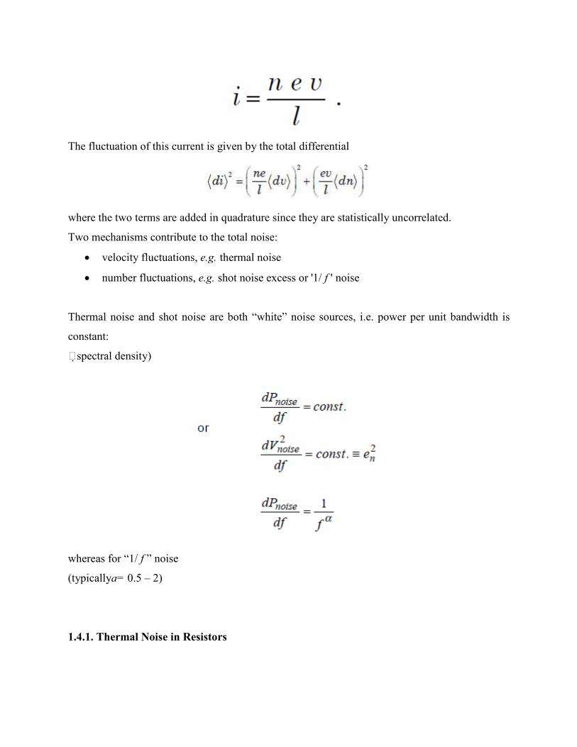
The fluctuation of this current is given by the total differential
where the two terms are added in quadrature since they are statistically uncorrelated.
Two mechanisms contribute to the total noise:
• velocity fluctuations, e.g.
• number fluctuations, e.g.
Thermal noise and shot noise are both “white” noise sources, i.e. power per unit bandwidth is
constant:
=spectral density)
whereas for “1/ f ” noise
(typicallya= 0.5 – 2)
1.4.1. Thermal Noise in Resistors
The fluctuation of this current is given by the total differential
where the two terms are added in quadrature since they are statistically uncorrelated.
Two mechanisms contribute to the total noise:
e.g. thermal noise
e.g. shot noise excess or '1/ f ' noise
Thermal noise and shot noise are both “white” noise sources, i.e. power per unit bandwidth is
1. Thermal Noise in Resistors
where the two terms are added in quadrature since they are statistically uncorrelated.
Thermal noise and shot noise are both “white” noise sources, i.e. power per unit bandwidth is
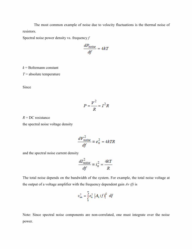
The most common example of noise due to velocity fluctuations is the thermal noise of
resistors.
Spectral noise power density vs. frequency
k = Boltzmann constant
T = absolute temperature
Since
R = DC resistance
the spectral noise voltage density
and the spectral noise current density
The total noise depends on the bandwidth of the system. For example, the total noise voltage at
the output of a voltage amplifier with the frequency dependent gain
Note: Since spectral noise components are non
power.
The most common example of noise due to velocity fluctuations is the thermal noise of
Spectral noise power density vs. frequency f
the spectral noise voltage density
and the spectral noise current density
The total noise depends on the bandwidth of the system. For example, the total noise voltage at
the output of a voltage amplifier with the frequency dependent gain Av (f) is
Note: Since spectral noise components are non-correlated, one must integrate ov
The most common example of noise due to velocity fluctuations is the thermal noise of
The total noise depends on the bandwidth of the system. For example, the total noise voltage at
correlated, one must integrate over the noise
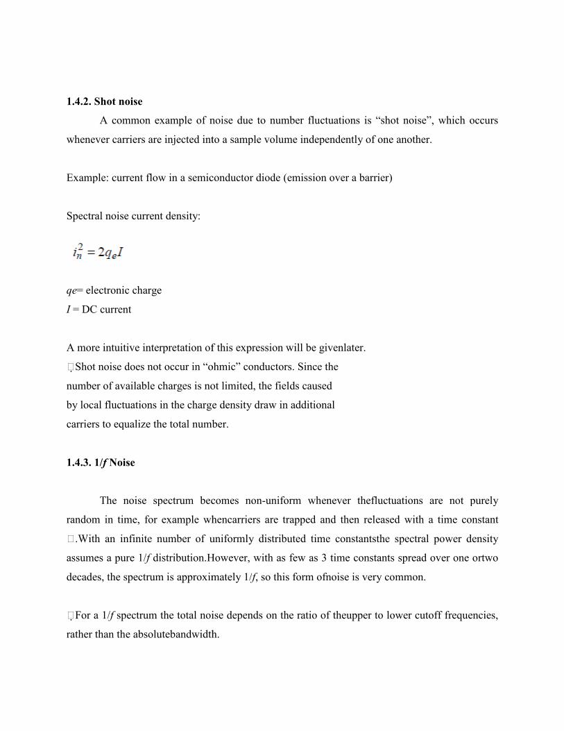
1.4.2. Shot noise
A common example of noise due to number fluctuations is “shot noise”, which occurs
whenever carriers are injected into a sample volume independently of one another.
Example: current flow in a semiconductor diode (emi
Spectral noise current density:
qe= electronic charge
I = DC current
A more intuitive interpretation of this expression will be givenlater.
=Shot noise does not occur in “ohmic” conductors. Since the
number of available charges is not limited, the fields caused
by local fluctuations in the charge density draw in additional
carriers to equalize the total number.
1.4.3. 1/f Noise
The noise spectrum becomes non
random in time, for example whencarriers are trapped and then released with a time constant
=.With an infinite number of uniformly distributed time constantsthe spectral power d
assumes a pure 1/f distribution.However, with as few as 3 time constants spread over one ortwo
decades, the spectrum is approximately 1/
=For a 1/f spectrum the total noise depends on the ratio of theupper to
rather than the absolutebandwidth.
A common example of noise due to number fluctuations is “shot noise”, which occurs
whenever carriers are injected into a sample volume independently of one another.
Example: current flow in a semiconductor diode (emission over a barrier)
A more intuitive interpretation of this expression will be givenlater.
=Shot noise does not occur in “ohmic” conductors. Since the
of available charges is not limited, the fields caused
by local fluctuations in the charge density draw in additional
carriers to equalize the total number.
The noise spectrum becomes non-uniform whenever thefluctuations are not purely
random in time, for example whencarriers are trapped and then released with a time constant
=.With an infinite number of uniformly distributed time constantsthe spectral power d
distribution.However, with as few as 3 time constants spread over one ortwo
decades, the spectrum is approximately 1/f, so this form ofnoise is very common.
spectrum the total noise depends on the ratio of theupper to lower cutoff frequencies,
rather than the absolutebandwidth.
A common example of noise due to number fluctuations is “shot noise”, which occurs
whenever carriers are injected into a sample volume independently of one another.
uniform whenever thefluctuations are not purely
random in time, for example whencarriers are trapped and then released with a time constant
=.With an infinite number of uniformly distributed time constantsthe spectral power density
distribution.However, with as few as 3 time constants spread over one ortwo
, so this form ofnoise is very common.
lower cutoff frequencies,
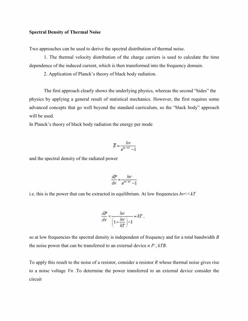
Spectral Density of Thermal Noise
Two approaches can be used to derive the spectral distribution of thermal noise.
1. The thermal velocity distribution of the charge carriers is used to calcul
dependence of the induced current, which is then transformed into the frequency domain.
2. Application of Planck’s theory of black body radiation.
The first approach clearly shows the underlying physics, whereas the second “hides” the
physics by applying a general result of statistical mechanics. However, the first requires some
advanced concepts that go well beyond the standard curriculum, so the “black body” approach
will be used.
In Planck’s theory of black body radiation the energy per mod
and the spectral density of the radiated power
i.e. this is the power that can be extracted in equilibrium. At low frequencies
so at low frequencies the spectral density is independent of frequency and for a total bandwidth
the noise power that can be transferred to an external device
To apply this result to the noise of a resistor, consider a resistor
to a noise voltage Vn .To determine the power transferred to an external device
circuit
Spectral Density of Thermal Noise
Two approaches can be used to derive the spectral distribution of thermal noise.
1. The thermal velocity distribution of the charge carriers is used to calcul
dependence of the induced current, which is then transformed into the frequency domain.
2. Application of Planck’s theory of black body radiation.
The first approach clearly shows the underlying physics, whereas the second “hides” the
by applying a general result of statistical mechanics. However, the first requires some
advanced concepts that go well beyond the standard curriculum, so the “black body” approach
In Planck’s theory of black body radiation the energy per mode
and the spectral density of the radiated power
i.e. this is the power that can be extracted in equilibrium. At low frequencies hv<<kT
so at low frequencies the spectral density is independent of frequency and for a total bandwidth
the noise power that can be transferred to an external device n P=kTB.
To apply this result to the noise of a resistor, consider a resistor R whose thermal noise gives rise
To determine the power transferred to an external device
1. The thermal velocity distribution of the charge carriers is used to calculate the time
dependence of the induced current, which is then transformed into the frequency domain.
The first approach clearly shows the underlying physics, whereas the second “hides” the
by applying a general result of statistical mechanics. However, the first requires some
advanced concepts that go well beyond the standard curriculum, so the “black body” approach
hv<<kT
so at low frequencies the spectral density is independent of frequency and for a total bandwidth B
whose thermal noise gives rise
To determine the power transferred to an external device consider the
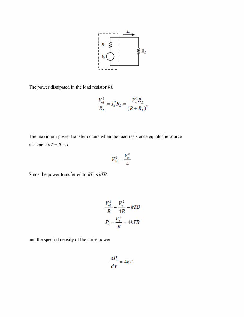
The power dissipated in the load resistor
The maximum power transfer occurs when the load resistance equals the source
resistanceRT = R, so
Since the power transferred to RL
and the spectral density of the noise power
The power dissipated in the load resistor RL
The maximum power transfer occurs when the load resistance equals the source
RL is kTB
the spectral density of the noise power
1.4.4 Spectral Density of Shot Noise
If an excess electron is injected into a device, it forms a current pulse of duration
thermionic diode t is the transit time from cathode to anode (see IX.2), for example. In a
semiconductor diode t is the recombination time (see IX
to the periods of interest t<<1/ f
transform of a delta pulse yields a “white” spectrum, i.e. the amplitude distribution in frequency
is uniform
Within an infinitesimally narrow frequency band the individual spectral components are pure
sinusoids, so their rms value
If N electrons are emitted at the same average rate, but at different times, they will have the same
spectral distribution, but the coefficients will differ in phase. For example, for two currents
iqwith a relative phase =the total rms current
For a random phase the third term averages to zero
so if N electrons are randomly emitted per unit time, the individual spectral components
simply add in quadrature
Spectral Density of Shot Noise
If an excess electron is injected into a device, it forms a current pulse of duration
is the transit time from cathode to anode (see IX.2), for example. In a
is the recombination time (see IX-2). If these times are short with respect
f , the current pulse can be represented by a d pulse
transform of a delta pulse yields a “white” spectrum, i.e. the amplitude distribution in frequency
Within an infinitesimally narrow frequency band the individual spectral components are pure
electrons are emitted at the same average rate, but at different times, they will have the same
spectral distribution, but the coefficients will differ in phase. For example, for two currents
the total rms current
random phase the third term averages to zero
electrons are randomly emitted per unit time, the individual spectral components
If an excess electron is injected into a device, it forms a current pulse of duration t. In a
is the transit time from cathode to anode (see IX.2), for example. In a
2). If these times are short with respect
pulse. The Fourier
transform of a delta pulse yields a “white” spectrum, i.e. the amplitude distribution in frequency
Within an infinitesimally narrow frequency band the individual spectral components are pure
electrons are emitted at the same average rate, but at different times, they will have the same
spectral distribution, but the coefficients will differ in phase. For example, for two currents ipand
electrons are randomly emitted per unit time, the individual spectral components
The average current
so the spectral noise density
“Noiseless” Resistances
a) Dynamic Resistance
In many instances a resistance is formed by the slope of a device’s current
characteristic, rather than by a static ensemble of electrons agitated by thermal energy.
Example: forward-biased semiconductor diode
Diode current vs. voltage
The differential resistance
i.e. at a given current the diode presents a resistance, e.g. 26
I = 1 mA and T = 300 K.
In many instances a resistance is formed by the slope of a device’s current
characteristic, rather than by a static ensemble of electrons agitated by thermal energy.
biased semiconductor diode
i.e. at a given current the diode presents a resistance, e.g. 26 =at
In many instances a resistance is formed by the slope of a device’s current-voltage
characteristic, rather than by a static ensemble of electrons agitated by thermal energy.
Note that two diodes can have different charge carrier concentrations, but will still exhibit the
same dynamic resistance at a given current, so the dynamic resistance is not uniquely determined
by the number of carriers, as in a resistor.
There is no thermal noise associated with this “dynamic” resistance, although the current
flow carries shot noise.
Radiation Resistance of an Antenna
Consider a receiving antenna with the normalized power pattern
P n(=,Ф) P pointing at a brightness distribution
bandwidth received by the antenna
wheree A is the effective aperture, i.e. the “capture area” of the antenna. For a given field
strength E, the captured power =
If the brightness distribution is from a black body radiator and we’re measuring in the Rayleigh
Jeans regime,
and the power received by the antenna
=A is the beam solid angle of the antenna (measured in rad2), i.e. the angle through which all the
power would flow if the antenna pattern were uniform over its beam width.
Since A e = A=λ=
(see antenna textbooks), the received p
The received power is independent of the radiation resistance, as would be expected for thermal
noise. However, it is not determined by the temperature of the antenna, but by the temperature of
the sky the antenna pattern is subtending.
Note that two diodes can have different charge carrier concentrations, but will still exhibit the
given current, so the dynamic resistance is not uniquely determined
by the number of carriers, as in a resistor.
There is no thermal noise associated with this “dynamic” resistance, although the current
Antenna
Consider a receiving antenna with the normalized power pattern
pointing at a brightness distribution B(=,Ф) in the sky. The power per unit
bandwidth received by the antenna
is the effective aperture, i.e. the “capture area” of the antenna. For a given field
=e W EA .
If the brightness distribution is from a black body radiator and we’re measuring in the Rayleigh
eceived by the antenna
is the beam solid angle of the antenna (measured in rad2), i.e. the angle through which all the
power would flow if the antenna pattern were uniform over its beam width.
(see antenna textbooks), the received power
The received power is independent of the radiation resistance, as would be expected for thermal
noise. However, it is not determined by the temperature of the antenna, but by the temperature of
the sky the antenna pattern is subtending.
Note that two diodes can have different charge carrier concentrations, but will still exhibit the
given current, so the dynamic resistance is not uniquely determined
There is no thermal noise associated with this “dynamic” resistance, although the current
Ф) in the sky. The power per unit
is the effective aperture, i.e. the “capture area” of the antenna. For a given field
If the brightness distribution is from a black body radiator and we’re measuring in the Rayleigh-
is the beam solid angle of the antenna (measured in rad2), i.e. the angle through which all the
The received power is independent of the radiation resistance, as would be expected for thermal
noise. However, it is not determined by the temperature of the antenna, but by the temperature of
For example, for a region dominated by the CMB, the measured power corresponds to a resistor
at a temperature of ~3K, although the antenna may be at 300K.
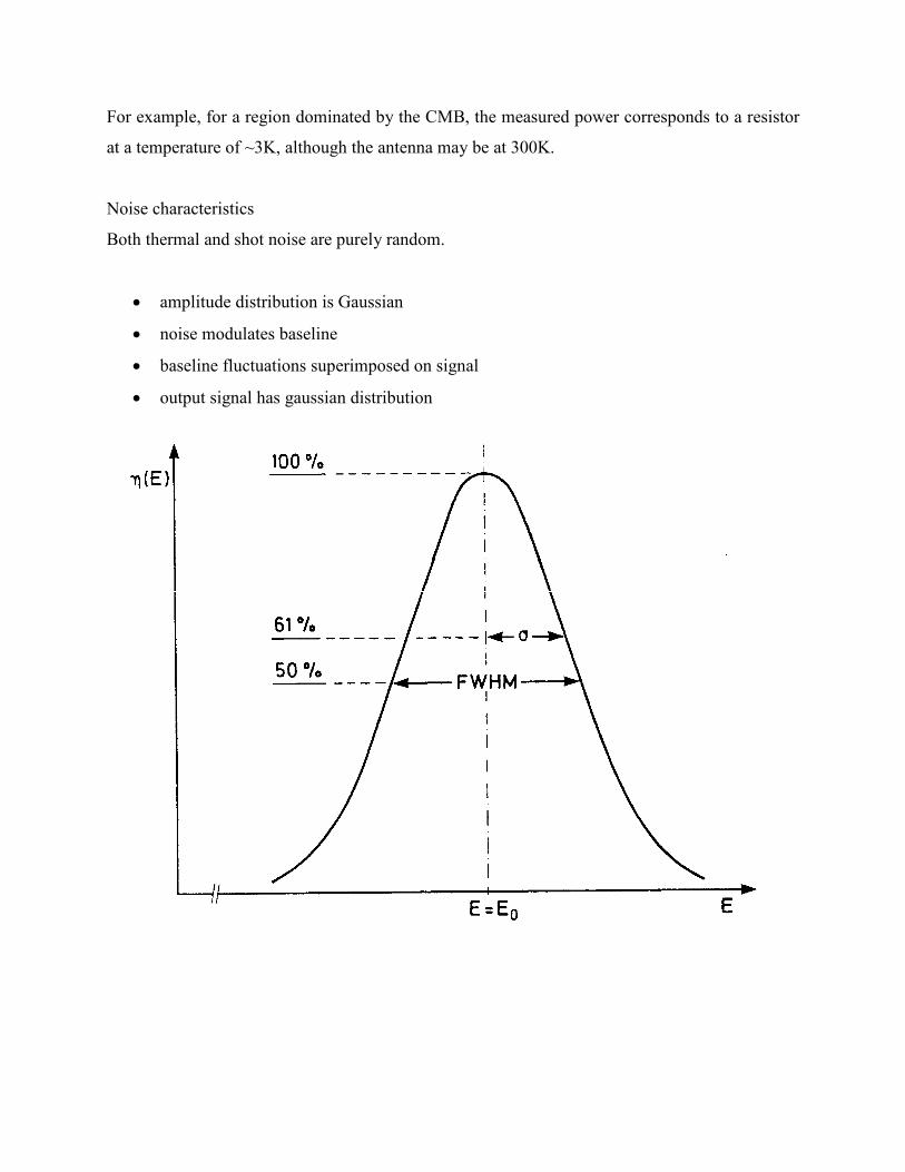
Noise characteristics
Both thermal and shot noise are purely random.
• amplitude distribution is Gaussian
• noise modulates baseline
• baseline fluctuations superimposed on signal
• output signal has gaussian distribution
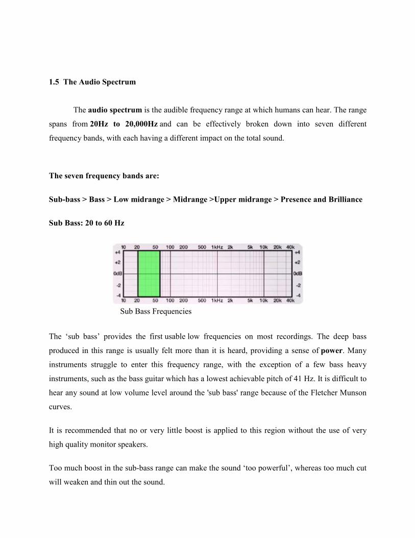
1.5 The Audio Spectrum
The audio spectrum is the audible frequency range at which humans can hear. The range
spans from 20Hz to 20,000Hz and can be effectively broken down into seven different
frequency bands, with each having a different impact on the total sound.
The seven frequency bands are:
Sub-bass > Bass > Low midrange > Midrange >Upper midrange > Presence and Brilliance
Sub Bass: 20 to 60 Hz
Sub Bass Frequencies
The ‘sub bass’ provides the first usable low frequencies on most recordings. The deep bass
produced in this range is usually felt more than it is heard, providing a sense of power. Many
instruments struggle to enter this frequency range, with the exception of a few bass heavy
instruments, such as the bass guitar which has a lowest achievable pitch of 41 Hz. It is difficult to
hear any sound at low volume level around the 'sub bass' range because of the Fletcher Munson
curves.
It is recommended that no or very little boost is applied to this region without the use of very
high quality monitor speakers.
Too much boost in the sub-bass range can make the sound ‘too powerful’, whereas too much cut
will weaken and thin out the sound.
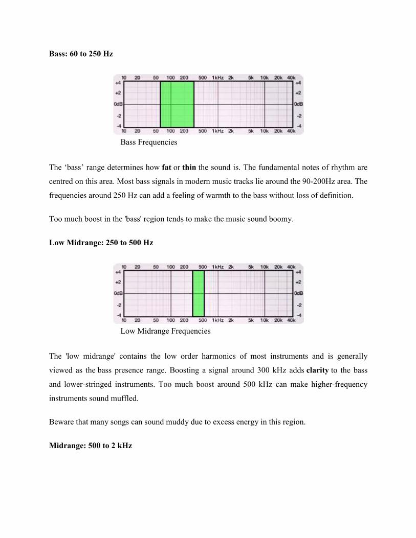
Bass: 60 to 250 Hz
Bass Frequencies
The ‘bass’ range determines how fat or thin the sound is. The fundamental notes of rhythm are
centred on this area. Most bass signals in modern music tracks lie around the 90-200Hz area. The
frequencies around 250 Hz can add a feeling of warmth to the bass without loss of definition.
Too much boost in the 'bass' region tends to make the music sound boomy.
Low Midrange: 250 to 500 Hz
Low Midrange Frequencies
The 'low midrange' contains the low order harmonics of most instruments and is generally
viewed as the bass presence range. Boosting a signal around 300 kHz adds clarity to the bass
and lower-stringed instruments. Too much boost around 500 kHz can make higher-frequency
instruments sound muffled.
Beware that many songs can sound muddy due to excess energy in this region.
Midrange: 500 to 2 kHz
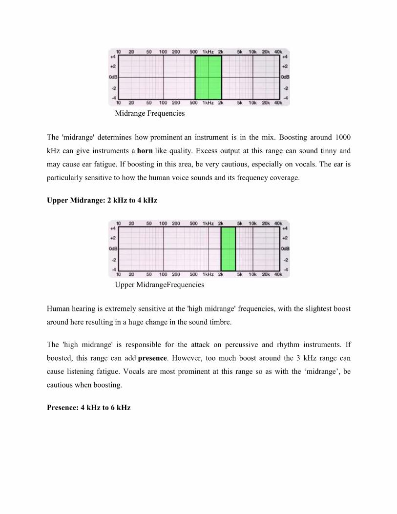
Midrange Frequencies
The 'midrange' determines how prominent an instrument is in the mix. Boosting around 1000
kHz can give instruments a horn like quality. Excess output at this range can sound tinny and
may cause ear fatigue. If boosting in this area, be very cautious, especially on vocals. The ear is
particularly sensitive to how the human voice sounds and its frequency coverage.
Upper Midrange: 2 kHz to 4 kHz
Upper MidrangeFrequencies
Human hearing is extremely sensitive at the 'high midrange' frequencies, with the slightest boost
around here resulting in a huge change in the sound timbre.
The 'high midrange' is responsible for the attack on percussive and rhythm instruments. If
boosted, this range can add presence. However, too much boost around the 3 kHz range can
cause listening fatigue. Vocals are most prominent at this range so as with the ‘midrange’, be
cautious when boosting.
Presence: 4 kHz to 6 kHz
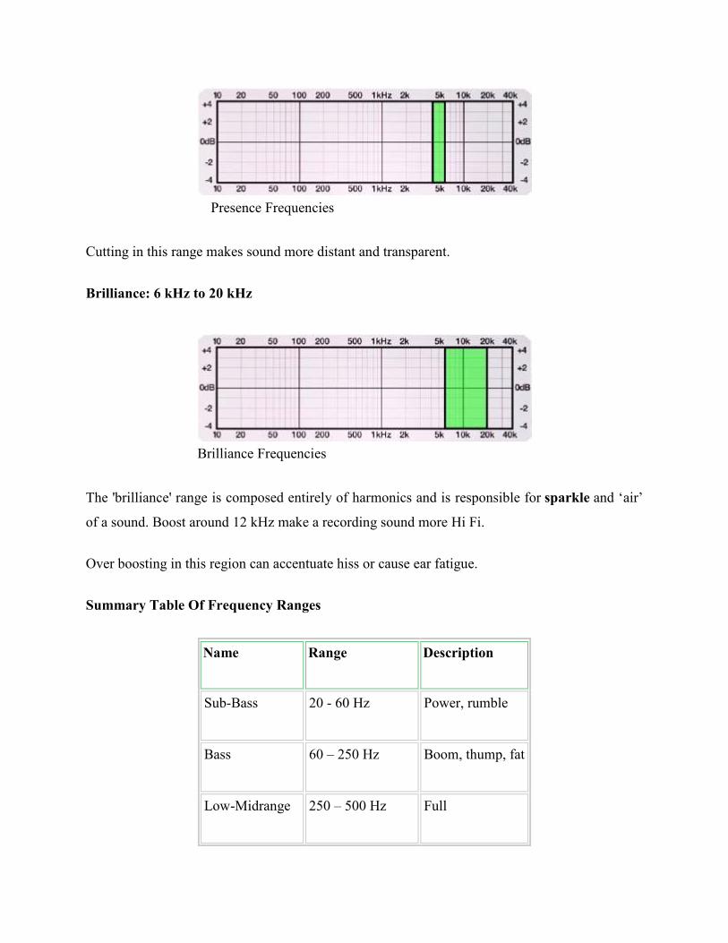
Presence Frequencies
Cutting in this range makes sound more distant and transparent.
Brilliance: 6 kHz to 20 kHz
Brilliance Frequencies
The 'brilliance' range is composed entirely of harmonics and is responsible for sparkle and ‘air’
of a sound. Boost around 12 kHz make a recording sound more Hi Fi.
Over boosting in this region can accentuate hiss or cause ear fatigue.
Summary Table Of Frequency Ranges
Name Range Description
Sub-Bass 20 - 60 Hz Power, rumble
Bass 60 – 250 Hz Boom, thump, fat
Low-Midrange 250 – 500 Hz Full
Midrange 500 – 2000 Hz Horn , cheap
Upper-Midrange 2000 – 4000 Hz Prominent, Horn
Presence 4000 – 6000 Hz Clear, bright
Brilliance 6000 – 20, 000 Hz Air, sparkle
1.6 Signal power Units& volume units
Electronic noise is a random fluctuation in an electrical signal, a characteristic of
all electronic circuits. Noise generated by electronic devices varies greatly, as it can be produced
by several different effects. Thermal noise is unavoidable at non-zero temperature, while other
types depend mostly on device type or manufacturing quality and semiconductor defects (such as
conductance fluctuations, including 1/f noise).
In communication systems, the noise is an error or undesired random disturbance of a useful
information signal, introduced before or after the detector and decoder. The noise is a summation
of unwanted or disturbing energy from natural and sometimes man-made sources. Noise is,
however, typically distinguished from interference, (e.g. cross-talk, deliberate jamming or other
unwanted electromagnetic interference from specific transmitters), for example in the signal-to-
noise ratio (SNR), signal-to-interference ratio (SIR) and signal-to-noise plus interference
ratio (SNIR) measures. Noise is also typically distinguished from distortion, which is an
unwanted alteration of the signal waveform, for example in the signal-to-noise and distortion
ratio (SINAD). In a carrier-modulated passband analog communication system, a certain carrier-
to-noise ratio (CNR) at the radio receiver input would result in a certain signal-to-noise ratio in
the detected message signal. In a digital communications system, a certain Eb/N0 (normalized
signal-to-noise ratio) would result in a certain bit error rate (BER).
1.7 Summary
Analog signals are time varying voltages or currents that are continuously changing ,
such as sine and cosine waves. An analog signal contains an infinite number of values. Digital
signals are voltages or currents that change in discrete steps or levels. The most common form of
digital signal is binary, which has two levels. All forms of information, however, must be
converted to electromagnetic energy before being propagated through an electronic
communication system.
Contamination problems have become a major factor in determining the
manufacturability, quality, and reliability of electronic assemblies. Understanding the mechanics
and chemistry of contamination has become necessary for improving quality and reliability and
reducing costs of electronic assemblies. Electronic noise is a random fluctuation in an electrical
signal, a characteristic of all electronic circuits. Noise generated by electronic devices varies
greatly, as it can be produced by several different effects. The audio spectrum is the audible
frequency range at which humans can hear.
1.8 Keywords
• Electronic noise
• Power
• Audio spectrum
1.9 Exercise
1. Explain Contaminations.
2. Describe the Audio Spectrum.
3. Explain the Spectral Density of Thermal Noise
Unit 2
Electronic Communication System-2
Structure
2.1 Introduction
2.2 Objectives
2.3 Signal-to-noise-ratio
2.4 Analog and digital signals
2.5 Modulation
2.6 Fundamental Limitations In A Communication System
2.7Number System
2.8 Summary
2.9 Keywords
2.10 Exercise
2.1 Introduction
There are two types of signals that carry information - analog and digital signals. The
difference between analog and digital signals is that analog is a continuous electrical signal,
whereas digital is a non-continuous electrical signal.Modulation is the process of varying some
characteristic of a periodic wave with external signals. Modulation is utilized to send an
information bearing signal over long distances.Bandwidth is the information-carrying capacity of
a communication channel. The channel may be analog or digital.
2.2 Objectives
At the end of this chapter you will be able to:
• Explain the Signal-to-noise-ratio
• Know Analog and digital signals
• Explain Modulation
• Know the Limitations In A Communication System
2.3 Signal-to-noise-ratio
The arch enemy of picture clarity on a monitor is noise, this is electronic noise that is
present to some extent in all video signals. Noise manifests itself as snow or graininess over the
whole picture on the monitor. There are several sources of noise; poor circuit design, heat, over-
amplification, external influences, automatic gain control, transmission systems such as
microwave, infrared etc. The important factor that determines the tolerance of noise is the
amount of noise in the video signal, the signal to noise ratio. Note that every time that a video
signal is processed in any way, noise is introduced.
The S/N ratio is exceedingly difficult to measure without special (and very expensive)
test equipment. For instance to test for S/N ratio could cost in the region of £25,000 for the
equipment. A less expensive way is to introduce a special filter to exclude the video signal and
measure the remaining noise, from which the S/N ratio can be calculated. However even this
filter can cost in the order of £1,000. Neither of these methods are practical in the field on actual
installations, even if the equipment could be afforded.
This leaves the problem that when viewing the picture on an installed system, the
assessment of the amount of noise is very subjective. One persons idea of a ‘noisy’ picture is not
necessarily anothers. The quality of the picture can also be aggravated by other factors as mains
hum, transmission losses, etc. These can be generally be overcome by isolation transformers,
video line correctors, using twisted pair transmission etc. However the noise cannot be reduced
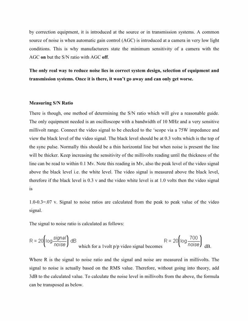
by correction equipment, it is introduced at the source or in transmission systems. A common
source of noise is when automatic gain control (AGC) is introduced at a camera in very low light
conditions. This is why manufacturers state the minimum sensitivity of a camera with the
AGC on but the S/N ratio with AGC off.
The only real way to reduce noise lies in correct system design, selection of equipment and
transmission systems. Once it is there, it won’t go away and can only get worse.
Measuring S/N Ratio
There is though, one method of determining the S/N ratio which will give a reasonable guide.
The only equipment needed is an oscilloscope with a bandwidth of 10 MHz and a very sensitive
millivolt range. Connect the video signal to be checked to the ‘scope via a 75W impedance and
view the black level of the video signal. The black level should be at 0.3 volts which is the top of
the sync pulse. Normally this should be a thin horizontal line but when noise is present the line
will be thicker. Keep increasing the sensitivity of the millivolts reading until the thickness of the
line can be read to within 0.1 Mv. Note this reading in Mv, also the peak level of the video signal
above the black level i.e. the white level. The video signal is measured above the black level,
therefore if the black level is 0.3 v and the video white level is at 1.0 volts then the video signal
is
1.0-0.3=.07 v. Signal to noise ratios are calculated from the peak to peak value of the video
signal.
The signal to noise ratio is calculated as follows:
which for a 1volt p/p video signal becomes dB.
Where R is the signal to noise ratio and the signal and noise are measured in millivolts. The
signal to noise is actually based on the RMS value. Therefore, without going into theory, add
3dB to the calculated value. To calculate the noise level in millivolts from the above, the formula
can be transposed as below.
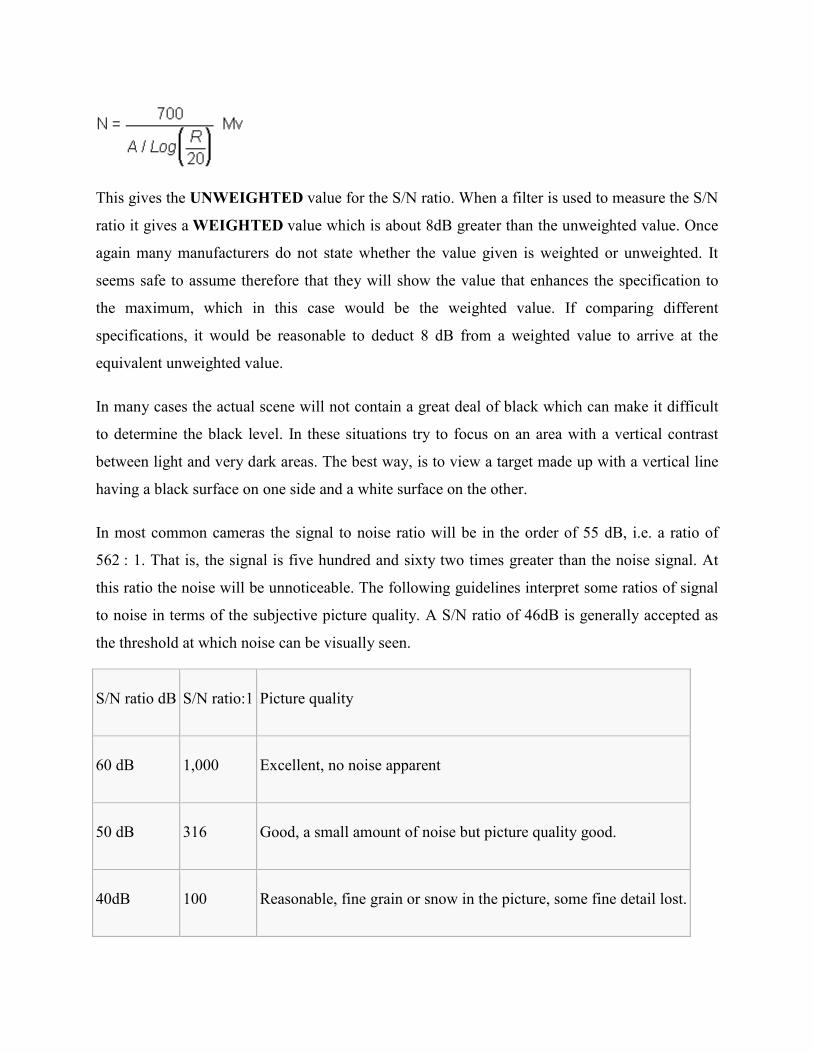
This gives the UNWEIGHTED value for the S/N ratio. When a filter is used to measure the S/N
ratio it gives a WEIGHTED value which is about 8dB greater than the unweighted value. Once
again many manufacturers do not state whether the value given is weighted or unweighted. It
seems safe to assume therefore that they will show the value that enhances the specification to
the maximum, which in this case would be the weighted value. If comparing different
specifications, it would be reasonable to deduct 8 dB from a weighted value to arrive at the
equivalent unweighted value.
In many cases the actual scene will not contain a great deal of black which can make it difficult
to determine the black level. In these situations try to focus on an area with a vertical contrast
between light and very dark areas. The best way, is to view a target made up with a vertical line
having a black surface on one side and a white surface on the other.
In most common cameras the signal to noise ratio will be in the order of 55 dB, i.e. a ratio of
562 : 1. That is, the signal is five hundred and sixty two times greater than the noise signal. At
this ratio the noise will be unnoticeable. The following guidelines interpret some ratios of signal
to noise in terms of the subjective picture quality. A S/N ratio of 46dB is generally accepted as
the threshold at which noise can be visually seen.
S/N ratio dB S/N ratio:1 Picture quality
60 dB 1,000 Excellent, no noise apparent
50 dB 316 Good, a small amount of noise but picture quality good.
40dB 100 Reasonable, fine grain or snow in the picture, some fine detail lost.
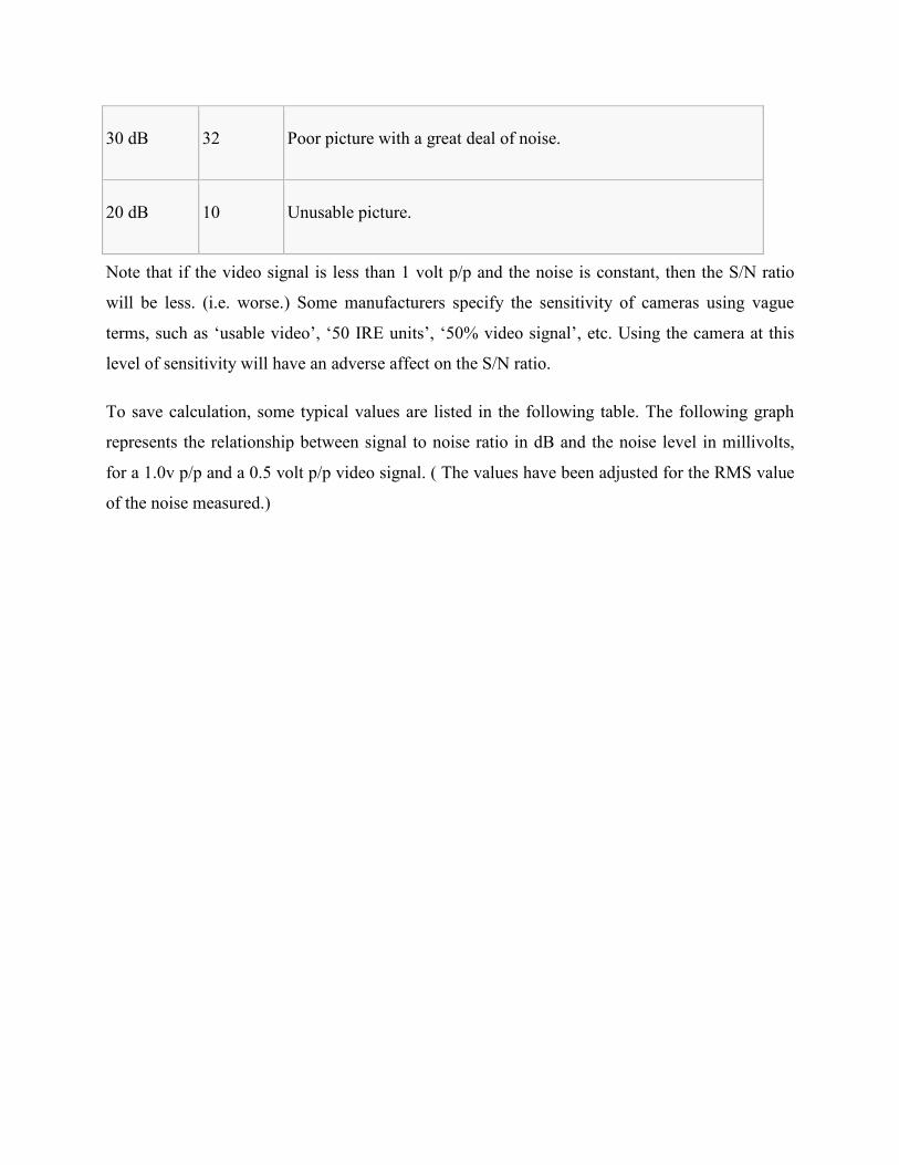
30 dB 32 Poor picture with a great deal of noise.
20 dB 10 Unusable picture.
Note that if the video signal is less than 1 volt p/p and the noise is constant, then the S/N ratio
will be less. (i.e. worse.) Some manufacturers specify the sensitivity of cameras using vague
terms, such as ‘usable video’, ‘50 IRE units’, ‘50% video signal’, etc. Using the camera at this
level of sensitivity will have an adverse affect on the S/N ratio.
To save calculation, some typical values are listed in the following table. The following graph
represents the relationship between signal to noise ratio in dB and the noise level in millivolts,
for a 1.0v p/p and a 0.5 volt p/p video signal. ( The values have been adjusted for the RMS value
of the noise measured.)
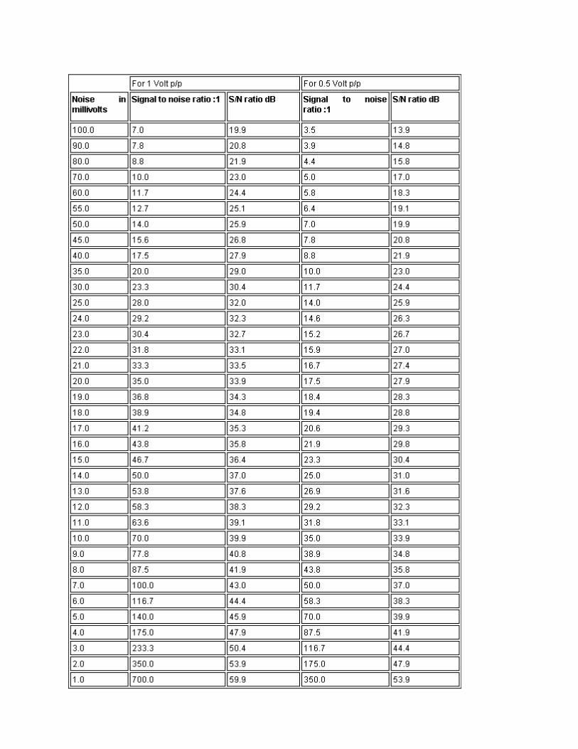
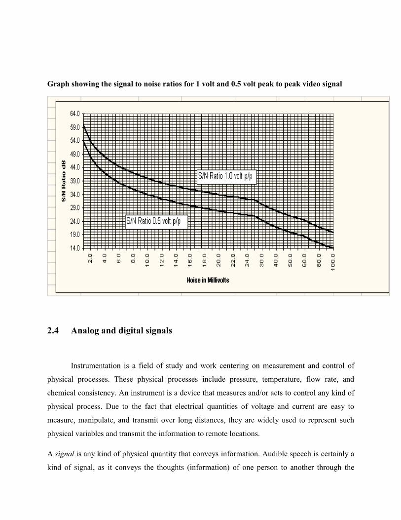
Graph showing the signal to noise ratios for 1 volt and 0.5 volt peak to peak video signal
2.4 Analog and digital signals
Instrumentation is a field of study and work centering on measurement and control of
physical processes. These physical processes include pressure, temperature, flow rate, and
chemical consistency. An instrument is a device that measures and/or acts to control any kind of
physical process. Due to the fact that electrical quantities of voltage and current are easy to
measure, manipulate, and transmit over long distances, they are widely used to represent such
physical variables and transmit the information to remote locations.
A signal is any kind of physical quantity that conveys information. Audible speech is certainly a
kind of signal, as it conveys the thoughts (information) of one person to another through the
physical medium of sound. Hand gestures are signals, too, conveying information by means of
light. This text is another kind of signal, interpreted by your English-trained mind as information
about electric circuits. In this chapter, the word signal will be used primarily in reference to an
electrical quantity of voltage or current that is used to represent or signify some other physical
quantity.
An analog signal is a kind of signal that is continuously variable, as opposed to having a limited
number of steps along its range (called digital). A well-known example of analog vs. digital is
that of clocks: analog being the type with pointers that slowly rotate around a circular scale, and
digital being the type with decimal number displays or a "second-hand" that jerks rather than
smoothly rotates. The analog clock has no physical limit to how finely it can display the time, as
its "hands" move in a smooth, pauseless fashion. The digital clock, on the other hand, cannot
convey any unit of time smaller than what its display will allow for. The type of clock with a
"second-hand" that jerks in 1-second intervals is a digital device with a minimum resolutionof
one second.
Both analog and digital signals find application in modern electronics, and the distinctions
between these two basic forms of information is something to be covered in much greater detail
later in this book. For now, I will limit the scope of this discussion to analog signals, since the
systems using them tend to be of simpler design.
With many physical quantities, especially electrical, analog variability is easy to come by. If
such a physical quantity is used as a signal medium, it will be able to represent variations of
information with almost unlimited resolution.
In the early days of industrial instrumentation, compressed air was used as a signaling medium to
convey information from measuring instruments to indicating and controlling devices located
remotely. The amount of air pressure corresponded to the magnitude of whatever variable was
being measured. Clean, dry air at approximately 20 pounds per square inch (PSI) was supplied
from an air compressor through tubing to the measuring instrument and was then regulated by
that instrument according to the quantity being measured to produce a corresponding output
signal. For example, a pneumatic (air signal) level "transmitter" device set up to measure height
of water (the "process variable") in a storage tank would output a low air pressure when the tank
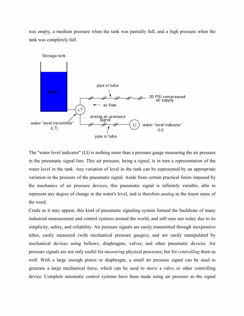
was empty, a medium pressure when the tank was partially full, and a high pressure when the
tank was completely full.
The "water level indicator" (LI) is nothing more than a pressure gauge measuring the air pressure
in the pneumatic signal line. This air pressure, being a signal, is in turn a representation of the
water level in the tank. Any variation of level in the tank can be represented by an appropriate
variation in the pressure of the pneumatic signal. Aside from certain practical limits imposed by
the mechanics of air pressure devices, this pneumatic signal is infinitely variable, able to
represent any degree of change in the water's level, and is therefore analog in the truest sense of
the word.
Crude as it may appear, this kind of pneumatic signaling system formed the backbone of many
industrial measurement and control systems around the world, and still sees use today due to its
simplicity, safety, and reliability. Air pressure signals are easily transmitted through inexpensive
tubes, easily measured (with mechanical pressure gauges), and are easily manipulated by
mechanical devices using bellows, diaphragms, valves, and other pneumatic devices. Air
pressure signals are not only useful for measuring physical processes, but for controlling them as
well. With a large enough piston or diaphragm, a small air pressure signal can be used to
generate a large mechanical force, which can be used to move a valve or other controlling
device. Complete automatic control systems have been made using air pressure as the signal
medium. They are simple, reliable, and relatively easy to understand. However, the practical
limits for air pressure signal accuracy can be too limiting in some cases, especially when the
compressed air is not clean and dry, and when the possibility for tubing leaks exist.
With the advent of solid-state electronic amplifiers and other technological advances, electrical
quantities of voltage and current became practical for use as analog instrument signaling media.
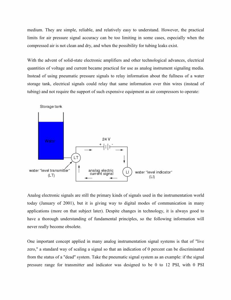
Instead of using pneumatic pressure signals to relay information about the fullness of a water
storage tank, electrical signals could relay that same information over thin wires (instead of
tubing) and not require the support of such expensive equipment as air compressors to operate:
Analog electronic signals are still the primary kinds of signals used in the instrumentation world
today (January of 2001), but it is giving way to digital modes of communication in many
applications (more on that subject later). Despite changes in technology, it is always good to
have a thorough understanding of fundamental principles, so the following information will
never really become obsolete.
One important concept applied in many analog instrumentation signal systems is that of "live
zero," a standard way of scaling a signal so that an indication of 0 percent can be discriminated
from the status of a "dead" system. Take the pneumatic signal system as an example: if the signal
pressure range for transmitter and indicator was designed to be 0 to 12 PSI, with 0 PSI
representing 0 percent of process measurement and 12 PSI representing 100 percent, a received
signal of 0 percent could be a legitimate reading of 0 percent measurement or it could mean that
the system was malfunctioning (air compressor stopped, tubing broken, transmitter
malfunctioning, etc.). With the 0 percent point represented by 0 PSI, there would be no easy way
to distinguish one from the other.
If, however, we were to scale the instruments (transmitter and indicator) to use a scale of 3 to 15
PSI, with 3 PSI representing 0 percent and 15 PSI representing 100 percent, any kind of a
malfunction resulting in zero air pressure at the indicator would generate a reading of -25 percent
(0 PSI), which is clearly a faulty value. The person looking at the indicator would then be able to
immediately tell that something was wrong.
Not all signal standards have been set up with live zero baselines, but the more robust signals
standards (3-15 PSI, 4-20 mA) have, and for good reason.
2.5 Modulation
Modulation is the process where a Radio Frequency or Light Wave's amplitude,
frequency, or phase is changed in order to transmit intelligence. The characteristics of the carrier
wave are instantaneously varied by another "modulating" waveform.
There are many ways to modulate a signal:
• Amplitude Modulation
• Frequency Modulation
• Phase Modulation
• Pulse Modulation
Additionally, digital signals usually require an intermediate modulation step for transport across
wideband, analog-oriented networks.
Amplitude Modulation (AM)
Amplitude Modulation occurs when a voice signal's varying voltage is applied to a carrier
frequency. The carrier frequency's amplitude changes in accordance with the modulated voice
signal, while the carrier's frequency does not change.
When combined the resultant AM signal consists of the carrier frequency, plus UPPER and
LOWER sidebands. This is known as Double Sideband - Amplitude Modulation (DSB-AM), or
more commonly referred to as plain AM.
The carrier frequency may be suppressed or transmitted at a relatively low level. This requires
that the carrier frequency be generated, or otherwise derived, at the receiving site for
demultiplexing. This type of transmission is known as Double Sideband - Suppressed Carrier
(DSB-SC).
It is also possible to transmit a SINGLE sideband for a slight sacrifice in low frequency response
(it is difficult to suppress the carrier and the unwanted sideband, without some low frequency
filtering as well). The advantage is a reduction in analog bandwidth needed to transmit the
signal. This type of modulation, known as Single Sideband - Suppressed Carrier (SSB-SC), is
ideal for Frequency Division Multiplexing (FDM).
Another type of analog modulation is known as Vestigial Sideband. Vestigial Sideband
modulation is a lot like Single Sideband, except that the carrier frequency is preserved and one of
the sidebands is eliminated through filtering. Analog bandwidth requirements are a little more
than Single Sideband however.
Vestigial Sideband transmission is usually found in television broadcasting. Such broadcast
channels require 6 MHz of ANALOG bandwidth, in which an Amplitude Modulated PICTURE
carrier is transmitted along with a Frequency Modulated SOUND carrier.
Frequency Modulation (FM)
Frequency Modulation occurs when a carrier's CENTER frequency is changed based upon the
input signal's amplitude. Unlike Amplitude Modulation, the carrier signal's amplitude is
UNCHANGED. This makes FM modulation more immune to noise than AM and improves the
overall signal-to-noise ratio of the communications system. Power output is also constant,
differing from the varying AM power output.
The amount of analog bandwidth necessary to transmit a FM signal is greater than the amount
necessary for AM, a limiting constraint for some systems.
Phase Modulation
Phase Modulation is similar to Frequency Modulation. Instead of the frequency of the carrier
wave changing, the PHASE of the carrier changes.
As you might imagine, this type of modulation is easily adaptable to data modulation
applications.
Pulse Modulation (PM)
With Pulse Modulation, a "snapshot" (sample) of the waveform is taken at regular intervals.
There are a variety of Pulse Modulation schemes:
• Pulse Amplitude Modulation
• Pulse Code Modulation
• Pulse Frequency Modulation
• Pulse Position Modulation
• Pulse Width Modulation
Pulse Amplitude Modulation (PAM)
In Pulse Amplitude Modulation, a pulse is generated with an amplitude corresponding to that of
the modulating waveform. Like AM, it is very sensitive to noise.
While PAM was deployed in early AT&T Dimension PBXs, there are no practical
implementations in use today. However, PAM is an important first step in a modulation scheme
known as Pulse Code Modulation.
Pulse Code Modulation (PCM)
In Pulse Code Modulation, PAM samples (collected at regular intervals) are quantized. That is to
say, the amplitude of the PAM pulse is assigned a digital value (number). This number is
transmitted to a receiver that decodes the digital value and outputs the appropriate analog pulse.
The fidelity of this modulation scheme depends upon the number of bits used to represent the
amplitude. The frequency range that can be represented through PCM modulation depends upon
the sample rate. To prevent a condition known as "aliasing", the sample rate MUST BE AT
LEAST twice that of the highest supported frequency. For typical voice channels (4 Khz
frequency range), the sample rate is 8 KHz.
Where is PCM today? Well, its EVERYWHERE! A typical PCM voice channel today operates
at 64 KBPS (8 bits/sample * 8000 samples/sec). But other PCM schemes are widely deployed in
today's audio (CD/DAT) and video systems!
Pulse Frequency Modulation (PFM)
With PFM, pulses of equal amplitude are generated at a rate modulated by the signal's frequency.
The random arrival rate of pulses makes this unsuitable for transmission through Time Division
Multiplexing (TDM) systems.
Pulse Position Modulation (PPM)
Also known as Pulse Time Modulation, PPM is a scheme where the pulses of equal amplitude
are generated at a rate controlled by the modulating signal's amplitude. Again, the random arrival
rate of pulses makes this unsuitable for transmission using TDM techniques.
Pulse Width Modulation (PWM)
In PWM, pulses are generated at a regular rate. The length of the pulse is controlled by the
modulating signal's amplitude. PWM is unsuitable for TDM transmission due to the varying
pulse width.
Digital Signal Modulation
Digital signals need to be processed by an intermediate stage for conversion into analog signals
for transmission. The device that accomplishes this conversion is known as a "Modem"
(MODulator/DEModulator).
2.6 Fundamental Limitations In A Communication System
The Fundamental Limitations In A Communication System are
• Noise
• Bandwidth
Noise
In communication systems, the noise is an error or undesired random disturbance of a useful
information signal, introduced before or after the detector and decoder. The noise is a summation
of unwanted or disturbing energy from natural and sometimes man-made sources. Noise is,
however, typically distinguished from interference, (e.g. cross-talk, deliberate jamming or other
unwanted electromagnetic interference from specific transmitters), for example in the signal-to-
noise ratio (SNR), signal-to-interference ratio (SIR) and signal-to-noise plus interference
ratio (SNIR) measures. Noise is also typically distinguished from distortion, which is an
unwanted alteration of the signal waveform, for example in the signal-to-noise and distortion
ratio (SINAD). In a carrier-modulated passband analog communication system, a certain carrier-
to-noise ratio (CNR) at the radio receiver input would result in a certain signal-to-noise ratio in
the detected message signal. In a digital communications system, a certain Eb/N0 (normalized
signal-to-noise ratio) would result in a certain bit error rate (BER).
Bandwidth
Bandwidth is the information-carrying capacity of a communication channel. The channel may
be analog or digital. Analog transmissions such as telephone calls, AM and FM radio, and
television are measured in cycles per second (hertz or Hz). Digital transmissions are measured in
bits per second. For digital systems, the terms "bandwidth" and "capacity" are often used
interchangeably, and the actual transmission capabilities are referred to as the data transfer rate
(or just data rate).
2.7 Number System
This section will introduce some basic number system concepts and introduce number systems
useful in electrical and computer engineering.
The decimal number system
In childhood, people are often taught the fundamentals of counting by using their fingers.
Counting from one to ten is one of many milestones a child achieves on their way to becoming
educated members of society. We will review these basic facts on our way to gaining an
understanding of alternate number systems.
The child is taught that the fingers and thumbs can be used to count from one to ten. Extending
one finger represents a count of one; two fingers represents a count of two, and so on up to a
maximum count of ten. No fingers (or thumbs) refers to a count of zero.
The child is later taught that there are certain symbols called digits that can be used to represent
these counts. These digits are, of course:
Ten, of course, is a special case, since it is comprised of two digits.
Before we go deeper, we need a few fundamental definitions.
Digit
A digit is a symbol given to an element of a number system.
Radix
The radix, or base of a counting system is defined as the number of unique digits in a given
number system.
Back to our elementary example. We know that our hypothetical child can count from zero to ten
using their fingers and thumbs. There are ten unique digits in this counting system, therefore the
radix of our elementary counting system is ten.
We represent the radix of our counting system by putting the radix in subscript to the right of the
digits. For example,
represents 3 in decimal (base 10).
Our special case (ten) illustrates a fundamental rule of our number system that was not readily
apparent - what happens when the count exceeds the highest digit? Obviously, a new digit is
added, to the left of our original digit which is "worth more", or has a higher weight than our
original digit. (In reality, there *always* are digits to the left; we simply choose not to write
those digits to the left of the first nonzero.)
When our count exceeds the highest digit available, the next digit to the left is incremented and
the original digit is reset to zero. For example:
Because we are dealing with a base-10 system, each digit to the left of another digit is weighted
ten times higher. Using exponential notation, we can imagine the number 10 as representing:
The fundamentals of decimal arithmetic will not be expanded on in this lecture.
The binary number system
It is widely believed that the decimal system that we find so natural to use is a direct
consequence of a human being's ten fingers and thumbs being used for counting purposes. One
could easily imagine that a race of intelligent, six-fingered beings could quite possibly have
developed a base-six counting system. From this perspective, consider the hypothesis: the most
intuitive number system for an entity is that for which some natural means of counting exists.
Since our focus is electronic and computer sys
hand to the switch, arguably the most fundamental structure that can be used to represent a count.
The switch can represent one of two states;
definition of a digit, how many digits are required to represent the possible states of our switch?
Clearly, the answer is 2. We use the binary digits zero and one to represent the open and closed
states of the switch.
Bits and bytes
A bit is a digit in the binary counting system.
A nybble (also spelled nibble) is a binary number co
A byte, or octet is a binary number consisting of eight bits.
From our earlier definition of radix, the binary
subscript much like we do with decimals:
Counting
Similar to decimals, binary digits are weighted. Each bit is weighted twice as much as the bit to
the right of it:
Counting from one to ten (base 10) i
Basic binary arithmetic
Binary addition, subtraction, multiplication and division operations work essentially the same as
they do for decimals.
six counting system. From this perspective, consider the hypothesis: the most
intuitive number system for an entity is that for which some natural means of counting exists.
Since our focus is electronic and computer systems, we must narrow our focus from the human
, arguably the most fundamental structure that can be used to represent a count.
The switch can represent one of two states; either open, or closed. If we return to our original
definition of a digit, how many digits are required to represent the possible states of our switch?
Clearly, the answer is 2. We use the binary digits zero and one to represent the open and closed
is a digit in the binary counting system.
(also spelled nibble) is a binary number consisting of four bits.
is a binary number consisting of eight bits.
From our earlier definition of radix, the binary system has a radix of two. We use the radix in the
subscript much like we do with decimals:
Similar to decimals, binary digits are weighted. Each bit is weighted twice as much as the bit to
Counting from one to ten (base 10) in binary yields:
Binary addition, subtraction, multiplication and division operations work essentially the same as
six counting system. From this perspective, consider the hypothesis: the most
intuitive number system for an entity is that for which some natural means of counting exists.
tems, we must narrow our focus from the human
, arguably the most fundamental structure that can be used to represent a count.
either open, or closed. If we return to our original
definition of a digit, how many digits are required to represent the possible states of our switch?
Clearly, the answer is 2. We use the binary digits zero and one to represent the open and closed
system has a radix of two. We use the radix in the
Similar to decimals, binary digits are weighted. Each bit is weighted twice as much as the bit to
Binary addition, subtraction, multiplication and division operations work essentially the same as
For addition, you add equally-weighted bits, much like decimal addition (where you add equal
weighted digits) and carry as required to the left.
As you can see, a carry is generated in the
Subtraction works just like decimal arithmetic, using borrowing as required.
Here, a borrow is required, reducing
to .
Multiplication is straightforward also:
Division is left as an exercise to the student [hint: use long division].
Conversion between binary and decimal
When you consider a binary number in exponential
conversion:
...simply add up the factors.
weighted bits, much like decimal addition (where you add equal
weighted digits) and carry as required to the left.
As you can see, a carry is generated in the column which increments the column.
Subtraction works just like decimal arithmetic, using borrowing as required.
Here, a borrow is required, reducing the column to and changing the
Multiplication is straightforward also:
Division is left as an exercise to the student [hint: use long division].
Conversion between binary and decimal
When you consider a binary number in exponential form, you can easily perform a decimal
weighted bits, much like decimal addition (where you add equally-
column.
and changing the column
form, you can easily perform a decimal
To convert from decimal to binary, you can repeatedly divide the decimal by two until the result
of the division is zero. Starting from the rightmost bit, write 1 if the division has a remainder,
zero if it does not. For example, to convert the decimal 74 into binary:
* 74 / 2 = 37 remainder 0; -> 0
* 37 / 2 = 18 remainder 1; -> 10
* 18 / 2 = 9 remainder 0; -> 010
* 9 / 2 = 4 remainder 1; -> 1010
* 4 / 2 = 1 remainder 0; -> 01010
* 2 / 2 = 1 remainder 0; -> 001010
* 1 / 2 = 0 remainder 1; -> 1001010
The octal number system
The name octal implies eight, if you consider that an octagon has eight sides. Octal has a radix of
eight, and uses the following octal digits:
An octal number has the subscript 8.
Counting
Counting from one to ten (base 10) in octal yields:
Octal arithmetic
Octal arithmetic, like binary arithmetic, follows the same rules and patterns of decimal
arithmetic. As an exercise, verify the following:
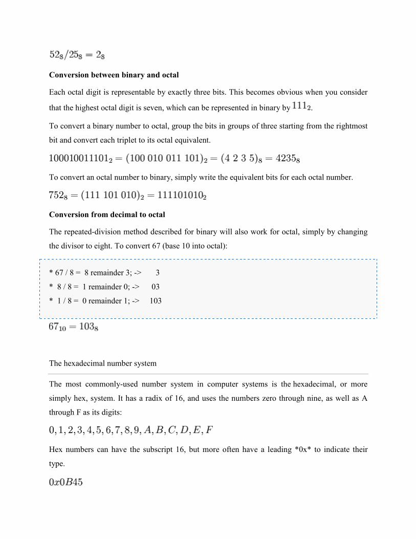
Conversion between binary and octal
Each octal digit is representable by exactly three bits. This becomes obvious when you consider
that the highest octal digit is seven, which can be represented in binary by
To convert a binary number to octal, group the bits in groups of three starting from the rightmost
bit and convert each triplet to its octal equivalent.
To convert an octal number to binary, simply wr
Conversion from decimal to octal
The repeated-division method described for binary will also work for octal, simply by changing
the divisor to eight. To convert 67 (base 10 into octal):
* 67 / 8 = 8 remainder 3; -> 3
* 8 / 8 = 1 remainder 0; -> 03
* 1 / 8 = 0 remainder 1; -> 103
The hexadecimal number system
The most commonly-used number system in computer systems is the
simply hex, system. It has a radix of 16, and uses the numbers zero through nine, as well as A
through F as its digits:
Hex numbers can have the subscript 16, bu
type.
Conversion between binary and octal
Each octal digit is representable by exactly three bits. This becomes obvious when you consider
it is seven, which can be represented in binary by .
To convert a binary number to octal, group the bits in groups of three starting from the rightmost
bit and convert each triplet to its octal equivalent.
To convert an octal number to binary, simply write the equivalent bits for each octal number.
Conversion from decimal to octal
division method described for binary will also work for octal, simply by changing
the divisor to eight. To convert 67 (base 10 into octal):
> 3
> 03
> 103
The hexadecimal number system
used number system in computer systems is the hexadecimal
simply hex, system. It has a radix of 16, and uses the numbers zero through nine, as well as A
Hex numbers can have the subscript 16, but more often have a leading *0x* to indicate their
Each octal digit is representable by exactly three bits. This becomes obvious when you consider
.
To convert a binary number to octal, group the bits in groups of three starting from the rightmost
ite the equivalent bits for each octal number.
division method described for binary will also work for octal, simply by changing
hexadecimal, or more
simply hex, system. It has a radix of 16, and uses the numbers zero through nine, as well as A
t more often have a leading *0x* to indicate their
Counting
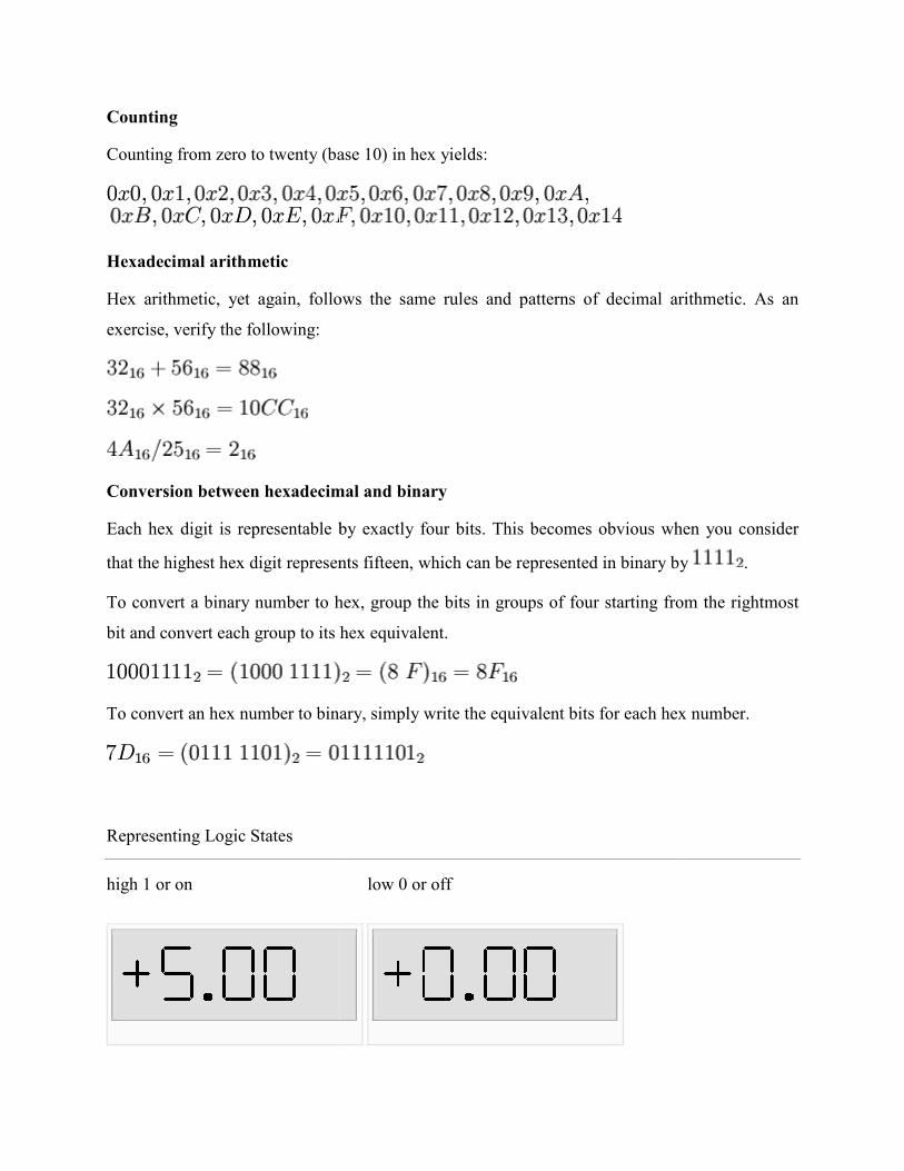
Counting from zero to twenty (base 10) in hex yields:
Hexadecimal arithmetic
Hex arithmetic, yet again, follows the same rules and patterns of decimal arithmetic. As an
exercise, verify the following:
Conversion between hexadecimal and binary
Each hex digit is representable by exactly four bits. This becomes obvious when you consider
that the highest hex digit represents fifteen, which can be represented in binary by
To convert a binary number to hex, group the bits in groups of four starting from the rightmost
bit and convert each group to its hex equivalent.
To convert an hex number to binary, simply write the equivalent bits for each hex number.
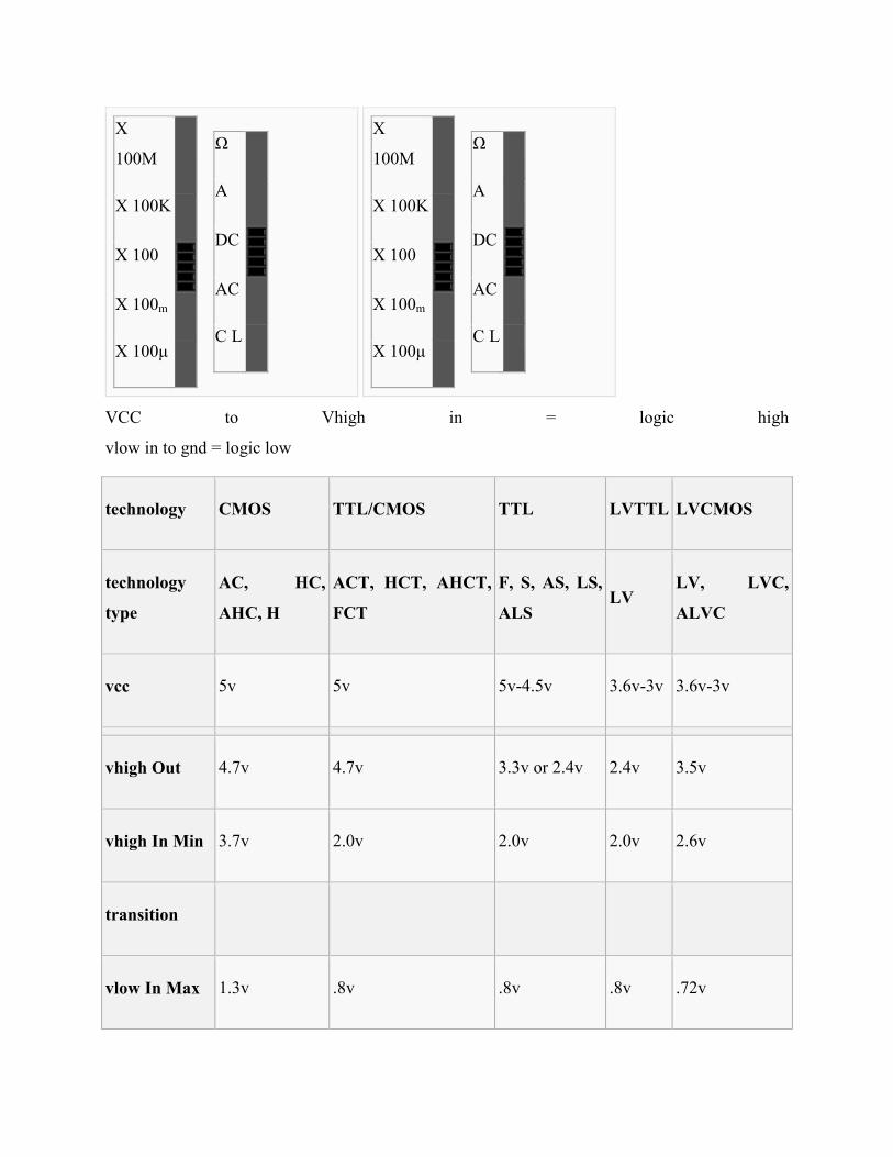
Representing Logic States
high 1 or on
Counting from zero to twenty (base 10) in hex yields:
Hex arithmetic, yet again, follows the same rules and patterns of decimal arithmetic. As an
Conversion between hexadecimal and binary
Each hex digit is representable by exactly four bits. This becomes obvious when you consider
that the highest hex digit represents fifteen, which can be represented in binary by
a binary number to hex, group the bits in groups of four starting from the rightmost
bit and convert each group to its hex equivalent.
To convert an hex number to binary, simply write the equivalent bits for each hex number.
low 0 or off
Hex arithmetic, yet again, follows the same rules and patterns of decimal arithmetic. As an
Each hex digit is representable by exactly four bits. This becomes obvious when you consider
that the highest hex digit represents fifteen, which can be represented in binary by .
a binary number to hex, group the bits in groups of four starting from the rightmost
To convert an hex number to binary, simply write the equivalent bits for each hex number.
X
100M
X 100K
X 100
X 100m
X 100µ
Ω
A
DC
AC
C L
X
100M
X 100K
X 100
X 100m
X 100µ
Ω
A
DC
AC
C L
VCC to Vhigh in = logic high
vlow in to gnd = logic low
technology CMOS TTL/CMOS TTL LVTTL LVCMOS
technology
type
AC, HC,
AHC, H
ACT, HCT, AHCT,
FCT
F, S, AS, LS,
ALS LV
LV, LVC,
ALVC
vcc 5v 5v 5v-4.5v 3.6v-3v 3.6v-3v
vhigh Out 4.7v 4.7v 3.3v or 2.4v 2.4v 3.5v
vhigh In Min 3.7v 2.0v 2.0v 2.0v 2.6v
transition
vlow In Max 1.3v .8v .8v .8v .72v
vlow Out .2v .2v .35v .4v .54v
Most 5v logic will have no problem with a 5V high or a 0V low. You should always refer to the
data sheet before choosing your device.
2.8 Summary
A signal is any kind of detectable quantity used to communicate
information.An analog signal is a signal that can be continuously, or infinitely, varied to
represent any small amount of change.Pneumatic, or air pressure, signals used to be used
predominately in industrial instrumentation signal systems. This has been largely superseded
by analog electrical signals such as voltage and current.A live zero refers to an analog signal
scale using a non-zero quantity to represent 0 percent of real-world measurement, so that any
system malfunction resulting in a natural "rest" state of zero signal pressure, voltage, or
current can be immediately recognized.Modulation is the process of varying some
characteristic of a periodic wave with external signals.Modulation is utilized to send an
information bearing signal over long distances.Bandwidth is the information-carrying
capacity of a communication channel. The channel may be analog or digital.
2.9 Keywords
• Ratio
• WEIGHTED
• Modulation
• AM
• FM
• Phase Modulation
• PM
• PAM
• PCM
• PFM
• PPM
• PWM
2.10 Exercise
1 Explain the Signal-to-noise-ratio.
2 Differentiate Analog and digital signals.
3 Explain Modulation.
4 Convert the following binary numbers to decimal:
5 Convert the following decimal numbers to binary:
6 Add the following numbers:
Unit 3
SAMPLING AND ANALOG PULSE MODULATION-1
Structure
3.1 Introduction
3.2 Objectives
3.3 Sampling Theory
3.4 Sampling Analysis
3.5 Types of sampling
3.6 Summary
3.7 Keywords
3.8 Exercise
3.1 Introduction
In signal processing, sampling is the reduction of a continuous signal to a discrete signal.
A common example is the conversion of a sound wave (a continuous signal) to a sequence of
samples (a discrete-time signal).
A sample refers to a value or set of values at a point in time and/or space.
A sampler is a subsystem or operation that extracts samples from a continuous signal. A
theoretical ideal sampler produces samples equivalent to the instantaneous value of the
continuous signal at the desired points.
3.2 Objectives
After studying this unit we are able to understand
− Sampling Theory
− Sampling Analysis
− Types of sampling
3.3 Sampling Theory
Sampling theory is derived as an application of the DTFT and the Fourier
theorems developed in Appendix C. First, we must derive a formula for aliasing due to
uniformly sampling a continuous-time signal. Next, the sampling theorem is proved. The
sampling theorem provides that a properly bandlimited continuous-time signal can be sampled
and reconstructed from its samples without error, in principle.
An early derivation of the sampling theorem is often cited as a 1928 paper by Harold Nyquist,
and Claude Shannon is credited with reviving interest in the sampling theorem after World War
II when computers became public.D.1As a result, the sampling theorem is often called ``Nyquist's
sampling theorem,'' ``Shannon's sampling theorem,'' or the like. Also, the sampling rate has been
called the Nyquist rate in honor of Nyquist's contributions [48]. In the author's experience,
however, modern usage of the term ``Nyquist rate'' refers instead to half the sampling rate. To
resolve this clash between historical and current usage, the term Nyquist limit will always
mean half the sampling rate in this book series, and the term ``Nyquist rate'' will not be used at
all.
3.4 Sampling Analysis
Sampling a continuous time signal produces a discrete time signal by selecting the values of the
continuous time signal at evenly spaced points in time. Thus, sampling a continuous time
signal x with sampling period Ts gives the discrete time signal xs defined by xs(n)=x(nTs). The
sampling angular frequency is then given by ωs=2π/Ts.
It should be intuitively clear that multiple continuous time signals sampled at the same rate can
produce the same discrete time signal since uncountably many continuous time functions could
be constructed that connect the points on the graph of any discrete time function. Thus, sampling
at a given rate does not result in an injective relationship. Hence, sampling is, in general, not
invertible.
EXAMPLE 1
For instance, consider the signals x,y defined by
x(t)=sin(t)t(1)
y(t)=sin(5t)t(2)
and their sampled versions xS,ys with sampling period Ts=π/2
xs(n)=sin(nπ/2)nπ/2(3)
ys(n)=sin(n5π/2)nπ/2.(4)
Notice that since
sin(n5π/2)=sin(n2π+nπ/2)=sin(nπ/2)(5)
it follows that
ys(n)=sin(nπ/2)nπ/2=xs(n).(6)
Hence, x and y provide an example of distinct functions with the same sampled versions at a
specific sampling rate.
It is also useful to consider the relationship between the frequency domain representations of the
continuous time function and its sampled versions. Consider a signal x sampled with sampling
period Ts to produce the discrete time signal xs(n)=x(nTs). The
spectrum Xs(ω) for ω∈[−π,π) of xs is given by
Xs(ω)=∑n=−∞∞x(nTs)e−jωn.(7)
Using the continuous time Fourier transform, x(tTs) can be represented as
x(tTs)=12πTs∫∞−∞X(ω1Ts)ejω1tdω1.(8)
Thus, the unit sampling period version of x(tTs), which is x(nTs) can be represented as
x(nTs)=12πTs∫∞−∞X(ω1Ts)ejω1ndω1.(9)
This is algebraically equivalent to the representation
x(nTs)=1Ts∑k=−∞∞12π∫π−πX(ω1−2πkTs)ej(ω1−2πk)ndω1,(10)
which reduces by periodicity of complex exponentials to
x(nTs)=1Ts∑k=−∞∞12π∫π−πX(ω1−2πkTs)ejω1ndω1.(11)
Hence, it follows that
Xs(ω)=1Ts∑k=−∞∞∑n=−∞∞(∫π−πX(ω1−2πkTs)ejω1ndω1)e−jωn.(12)
Noting that the above expression contains a Fourier series and inverse Fourier series pair, it
follows that
Xs(ω)=1Ts∑k=−∞∞X(ω−2πkTs).(13)
Hence, the spectrum of the sampled signal is, intuitively, the scaled sum of an infinite number of
shifted and time scaled copies of original signal spectrum. Aliasing, which will be discussed in
depth in later modules, occurs when these shifted spectrum copies overlap and sum together.
Note that when the original signal x is bandlimited to (−π/Ts,π/Ts) no overlap occurs, so each
period of the sampled signal spectrum has the same form as the orignal signal spectrum. This
suggest that if we sample a bandlimited signal at a sufficiently high sampling rate, we can
recover it from its samples as will be further described in the modules on the Nyquist-Shannon
sampling theorem and on perfect reconstruction.
3.5 Types of sampling
The various types of sampling, PCM, DM, DPCM etc
pulse code modulation (PCM)
Pulse code modulation (PCM) is a digital scheme for transmitting analogdata. The signals in
PCM are binary; that is, there are only two possible states, represented by logic 1 (high) and
logic0 (low). This is true no matter how complex the analog waveform happens to be. Using
PCM, it is possible to digitize all forms of analog data, including full-motion video, voices,
music, telemetry, and virtual reality (VR).
To obtain PCM from an analog waveform at the source (transmitter end) of a communications
circuit, the analog signal amplitude is sampled (measured) at regular time intervals.The sampling
rate, or number of samples per second, is several times the maximum frequency of the analog
waveform in cycles per second or hertz. The instantaneous amplitude of the analog signal at each
sampling is rounded off to the nearest of several specific, predetermined levels. This process is
called quantization. The number of levels is always a power of 2 -- for example, 8, 16, 32, or 64.
These numbers can be represented by three, four, five, or six binary digits (bits)respectively. The
output of a pulse code modulator is thus a series of binary numbers, each represented by some
power of 2bits.
At the destination (receiver end) of the communications circuit, a pulse code demodulator
converts the binary numbers back into pulses having the same quantum levels as those in the
modulator. These pulses are further processed to restore the original analog waveform.
Modulation
Modulation is the addition of information (or the signal) to an electronic or optical signal carrier.
Modulation can be applied to direct current (mainly by turning it on and off), to alternating
current, and to optical signals. One can think of blanket waving as a form of modulation used in
smoke signal transmission (the carrier being a steady stream of smoke).Morse code, invented for
telegraphy and still used in amateur radio, uses a binary (two-state) digital code similar to the
code used by modern computers. For most of radio and telecommunication today, the carrier is
alternating current (AC) in a given range of frequencies. Common modulation methods include:
Amplitude modulation (AM), in which the voltage applied to the carrier is varied over
time
Frequency modulation (FM), in which the frequency of the carrier waveform is varied in
small but meaningful amounts
Phase modulation (PM), in which the natural flow of the alternating current waveform
is delayed temporarily
These are sometimes known as continuous wave modulation methods to distinguish them from
pulse code modulation (PCM), which is used to encode both digital and analog information in a
binary way. Radio and television broadcaststations typically use AM or FM. Most two-way
radios use FM, although some employ a mode known as single sideband (SSB).
More complex forms of modulation are Phase Shift Keying (PSK) and Quadrature Amplitude
Modulation (QAM). Optical signals are modulated by applying an electromagnetic current to
vary the intensity of a laser beam.
Modem Modulation and Demodulation
A computer with an online or Internet connection that connects over a regular analog phone line
includes a modem. This term is derived by combining beginning letters from the words
modulator and demodulator. In a modem, the modulation process involves the conversion of the
digital computer signals (high and low, or logic 1 and 0 states) to analog audio-frequency
(AF)tones. Digital highs are converted to a tone having a certain constant pitch; digital lows are
converted to a tone having a different constant pitch. These states alternate so rapidly that,if you
listen to the output of a computer modem, it sounds like a hiss or roar. The demodulation process
converts the audio tones back into digital signals that a computer can understand. directly.
Multiplexing
More information can be conveyed in a given amount of time by dividing the bandwidth of a
signal carrier so that more than one modulated signal is sent on the same carrier. Known as
multiplexing, the carrier is sometimes referred to as a channel and each separate signal carried on
it is called a subchannel. (In some usages, each subchannel is known as a channel.) The device
that puts the separate signals on the carrier and takes them off of received transmissions is a
multiplexer. Common types of multiplexing include frequency-division multiplexing (FDM) and
time-division multiplexing (TDM). FDM is usually used for analog communication and divides
the main frequency of the carrier into separate subchannels, each with its own frequency band
within the overall bandwidth. TDM is used for digital communication and divides the main
signal into time-slots, with each time-slot carrying a separate signal.
Delta modulation and DPCM
PCM is powerful, but quite complex coders and decoders are required. An increase in resolution
also requires a higher number of bits per sample. Standard PCM systems have no memory —
each sample value is separately encoded into a series of binary digits. An alternative, which
overcomes some limitations of PCM is to use past information in the encoding process. One way
of doing this is to perform source coding using delta modulation:
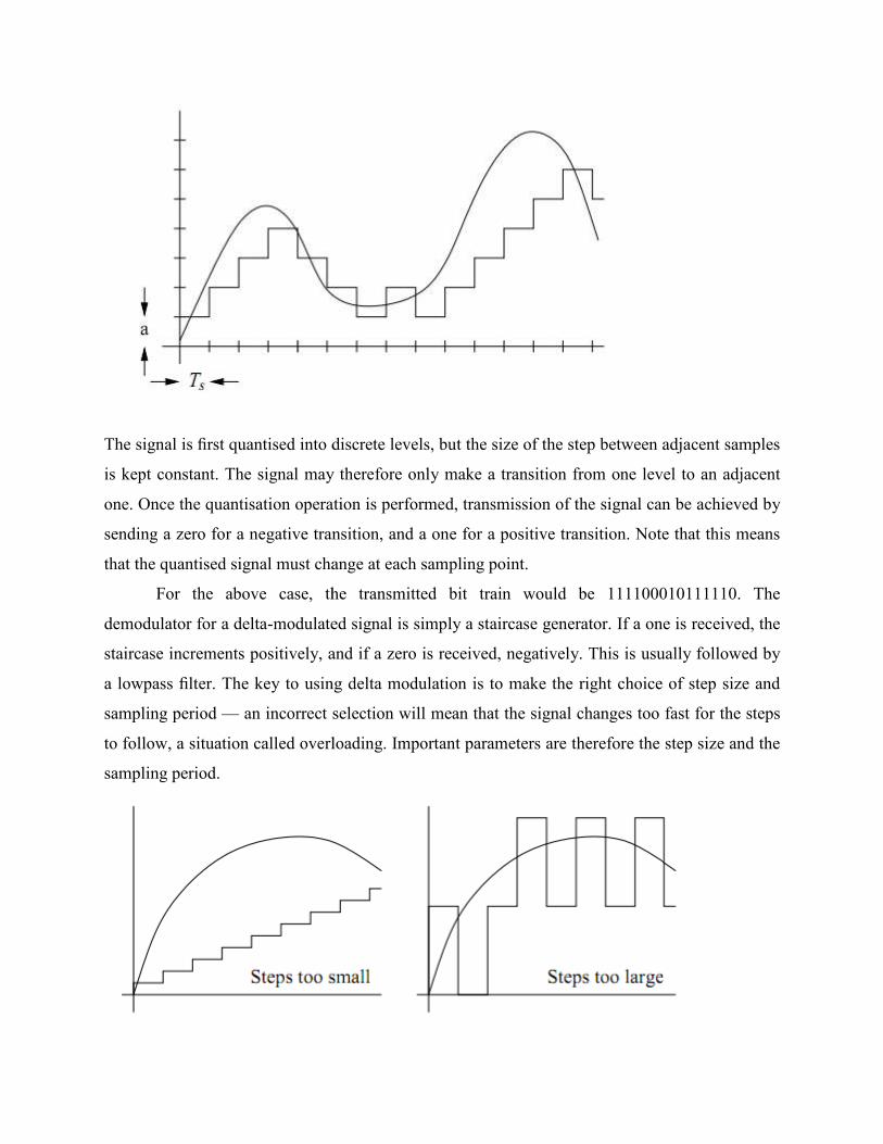
The signal is first quantised into discrete levels, but the size of the s
is kept constant. The signal may therefore only make a transition from one level to an adjacent
one. Once the quantisation operation is performed, transmission of the signal can be achieved by
sending a zero for a negative tran
that the quantised signal must change at each sampling point.
For the above case, the transmitted bit train would be 111100010111110. The
demodulator for a delta-modulated signal is simply a
staircase increments positively, and if a zero is received, negatively. This is usually followed by
a lowpass filter. The key to using delta modulation is to make the right choice of step size and
sampling period — an incorrect selection will mean that the signal changes too fast for the steps
to follow, a situation called overloading. Important parameters are therefore the step size and the
sampling period.
first quantised into discrete levels, but the size of the step between adjacent samples
is kept constant. The signal may therefore only make a transition from one level to an adjacent
one. Once the quantisation operation is performed, transmission of the signal can be achieved by
sending a zero for a negative transition, and a one for a positive transition. Note that this means
that the quantised signal must change at each sampling point.
For the above case, the transmitted bit train would be 111100010111110. The
modulated signal is simply a staircase generator. If a one is received, the
staircase increments positively, and if a zero is received, negatively. This is usually followed by
filter. The key to using delta modulation is to make the right choice of step size and
an incorrect selection will mean that the signal changes too fast for the steps
to follow, a situation called overloading. Important parameters are therefore the step size and the
tep between adjacent samples
is kept constant. The signal may therefore only make a transition from one level to an adjacent
one. Once the quantisation operation is performed, transmission of the signal can be achieved by
sition, and a one for a positive transition. Note that this means
For the above case, the transmitted bit train would be 111100010111110. The
staircase generator. If a one is received, the
staircase increments positively, and if a zero is received, negatively. This is usually followed by
filter. The key to using delta modulation is to make the right choice of step size and
an incorrect selection will mean that the signal changes too fast for the steps
to follow, a situation called overloading. Important parameters are therefore the step size and the
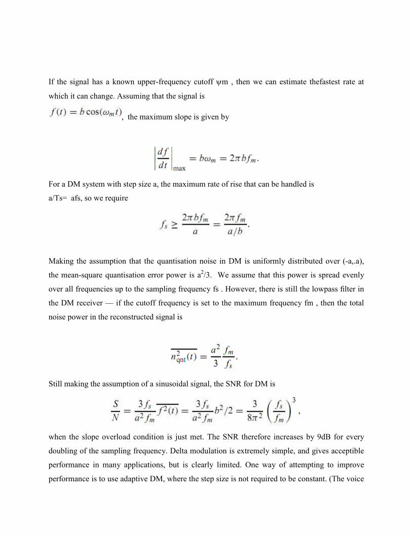
If the signal has a known upper
which it can change. Assuming that the signal is
, the maximum slope is given by
For a DM system with step size a, the maximum rate of rise that can be handled is
a/Ts= afs, so we require
Making the assumption that the quantisation noise in DM is uniformly distributed over (
the mean-square quantisation error power is a
over all frequencies up to the sampling frequency fs . However, the
the DM receiver — if the cutoff frequency is set to the maximum frequency fm , then the total
noise power in the reconstructed signal is
Still making the assumption of a sinusoidal signal, the SNR for DM is
when the slope overload condition is just met. The SNR therefore increases by 9dB for every
doubling of the sampling frequency. Delta modulation is extremely simple, and gives acceptible
performance in many applications, but is clearly limited. One way of attempting
performance is to use adaptive DM, where the step size is not required to be constant. (The voice
If the signal has a known upper-frequency cutoff ψm , then we can estimate thefastest rate at
which it can change. Assuming that the signal is
the maximum slope is given by
For a DM system with step size a, the maximum rate of rise that can be handled is
Making the assumption that the quantisation noise in DM is uniformly distributed over (
square quantisation error power is a2/3. We assume that this power is spread evenly
over all frequencies up to the sampling frequency fs . However, there is still the lowpass
if the cutoff frequency is set to the maximum frequency fm , then the total
noise power in the reconstructed signal is
Still making the assumption of a sinusoidal signal, the SNR for DM is
ope overload condition is just met. The SNR therefore increases by 9dB for every
doubling of the sampling frequency. Delta modulation is extremely simple, and gives acceptible
performance in many applications, but is clearly limited. One way of attempting
performance is to use adaptive DM, where the step size is not required to be constant. (The voice
m , then we can estimate thefastest rate at
For a DM system with step size a, the maximum rate of rise that can be handled is
Making the assumption that the quantisation noise in DM is uniformly distributed over (-a,.a),
/3. We assume that this power is spread evenly
re is still the lowpass filter in
if the cutoff frequency is set to the maximum frequency fm , then the total
ope overload condition is just met. The SNR therefore increases by 9dB for every
doubling of the sampling frequency. Delta modulation is extremely simple, and gives acceptible
performance in many applications, but is clearly limited. One way of attempting to improve
performance is to use adaptive DM, where the step size is not required to be constant. (The voice
communication systems on the US space shuttles make use of this technique.) Another is to use
delta PCM, where each desired step
size is encoded as a (multiple bit) PCM signal, and transmitted to the receiver as a code word.
Differential PCM is similar, but encodes the difference between a sample and its predicted value
— this can further reduce the number of bits required for transmission.
ADPCM
Short for Adaptive Differential Pulse Code Modulation, a form of pulse code modulation
(PCM) that produces a digital signal with a lower bit rate than standard PCM. ADPCM produces
a lower bit rate by recording only the difference between samples and adjusting the coding scale
dynamically to accommodate large and small differences. Some applications use ADPCM
todigitize a voice signal so voice and data can be transmitted simultaneously over a digital
facility normally used only for one or the other. Adaptive DPCM (ADPCM) is a variant
of DPCM (differential pulse-code modulation) that varies the size of the quantization step, to
allow further reduction of the required bandwidth for a given signal-to-noise ratio.Typically, the
adaptation to signal statistics in ADPCM consists simply of an adaptive scale factor before
quantizing the difference in the DPCM encoder.
3.6 Summary
Sampling a continuous time signal produces a discrete time signal by selecting the values
of the continuous time signal at equally spaced points in time. However, we have shown that this
relationship is not injective as multiple continuous time signals can be sampled at the same rate
to produce the same discrete time signal. This is related to a phenomenon called aliasing which
will be discussed in later modules. Consequently, the sampling process is not, in general,
invertible. Nevertheless, as will be shown in the module concerning reconstruction, the
continuous time signal can be recovered from its sampled version if some additional assumptions
hold.
PCM: The analog speech waveform is sampled and converted directly into a multibit
digital code by an A/D converter. The code is stored and subsequently recalled for
playback
DM: Only a single bit is stored for each sample. This bit 1 or 0, represents a greater than
or less than condition, respectively as compared to the previous sample. An integrator is
then used on the output to convert the stored nit stream to an analog signal.
DPCM: Stores a multibit difference value. A bipolar D/A converter is used for playback
to convert the successive difference values to an analog waveform.
ADPCM: Stores a difference value that has been mathematically adjusted according to
the slope of the input waveform. Bipolar D/A converter is used to convert the stored
digital code to analog for playback.
3.7 Keywords
PCM
DM
DPCM
ADPCM
3.8 Exercise
1. Give the full name of PCM, DM, DPCM and ADPCM. Describe their fundamental
differences.
2. Explain the sampling theory
3. Explain sampling analysis
4. What are different types of sampling?
Unit 4
SAMPLING AND ANALOG PULSE MODULATION-2
Structure
4.1 Introduction
4.2 Objectives
4.3 Types Of Analog Pulse modulation
4.4 Pulse-Amplitude Modulation (PAM)
4.5 Analog Pulse Density Modulation (PDM)
4.6 Analog Pulse Width Modulation
4.7 Pulse-position modulation (PPM)
4.8 Signal-To-Noise Ratios In Pulse Systems
4.9 Summary
4.10 Keywords
4.11 Exercise
4.1 Introduction
This chapter is dedicated to analog pulse modulation characterized by the use of an
analogreference input to the pulse modulator. It is attempted to devise modulation strategies
thatwill lead to the optimal PMA performance. This is carried out by a fundamental review
andcomparison of known pulse modulation methods, followed by investigations of newenhanced
pulse modulation methods with improved characteristics. The analysis is basedon the derivation
of Double Fourier Series (DFS) expressions for all considered methods,and the introduction for a
spectral analysis tool – the Harmonic Envelope Surface (HES) –based on the analytical DFS
expressions. The HES offers detailed insight in the (for PMAs)interesting aspects and the tool
proves indispensable of a coherent analysis and comparisonof extensive set of pulse modulation
methods that are investigated throughout this centralchapter. A new multi-level modulation
method – Phase Shifted Carrier Pulse WidthModulation (PSCPWM) [Ni97b] – is introduced and
subjected to a detailed investigation.A suite of PSCPWM methods are defined each with distinct
characteristics, and it willappear that the principle provides optimal pulse modulation for PMAs
from a theoreticalpoint of view.
4.2 Objectives
After studying this unit we are able to understand
− Types of Analog Pulse modulation
− Pulse-Amplitude Modulation (PAM)
− Analog Pulse Density Modulation (PDM)
− Analog Pulse Width Modulation
− Pulse-position modulation (PPM)
− Signal-To-Noise Ratios In Pulse Systems
4.3 Types Of Analog Pulse modulation
Pulse modulation systems represent a message-bearing signal by a train of pulses. The
fourbasic pulse modulation techniques are [Bl53] Pulse Amplitude Modulation (PAM),
PulseWidth Modulation (PWM), Pulse Position modulation (PPM) and Pulse Density
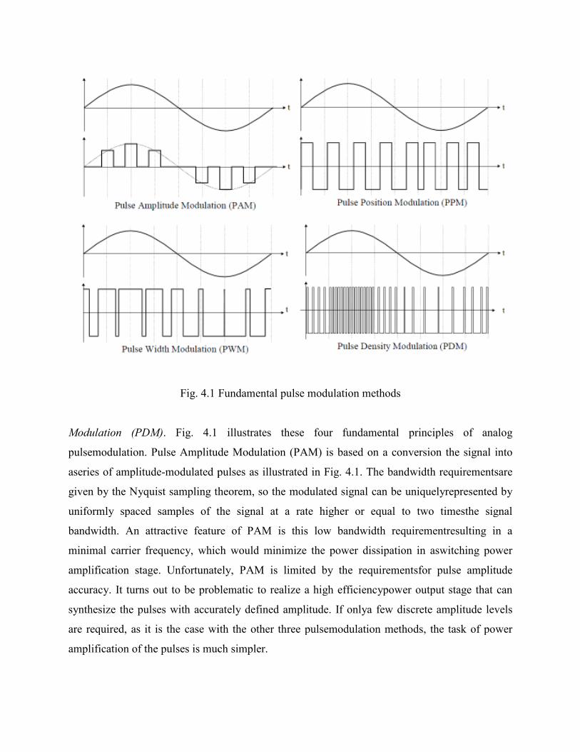
Fig. 4.1 Fundamental pulse modulation methods
Modulation (PDM). Fig. 4.1 illustrates these four fundamental principles of analog
pulsemodulation. Pulse Amplitude Modulation (PAM) is based on a conversion the signal into
aseries of amplitude-modulated puls
given by the Nyquist sampling theorem, so the modulated signal can be uniquelyrepresented by
uniformly spaced samples of the signal at a rate higher or equal to two timesthe signal
bandwidth. An attractive feature of PAM is this low bandwidth requirementresulting in a
minimal carrier frequency, which would minimize the power dissipation in aswitching power
amplification stage. Unfortunately, PAM is limited by the requirementsfor pulse amplitude
accuracy. It turns out to be problematic to realize a high efficiencypower output stage that can
synthesize the pulses with accurately defined amplitude. If onlya few discrete amplitude levels
are required, as it is the case with the other three pulsemodulat
amplification of the pulses is much simpler.
1 Fundamental pulse modulation methods
1 illustrates these four fundamental principles of analog
pulsemodulation. Pulse Amplitude Modulation (PAM) is based on a conversion the signal into
modulated pulses as illustrated in Fig. 4.1. The bandwidth requirementsare
given by the Nyquist sampling theorem, so the modulated signal can be uniquelyrepresented by
uniformly spaced samples of the signal at a rate higher or equal to two timesthe signal
attractive feature of PAM is this low bandwidth requirementresulting in a
minimal carrier frequency, which would minimize the power dissipation in aswitching power
amplification stage. Unfortunately, PAM is limited by the requirementsfor pulse amplitude
curacy. It turns out to be problematic to realize a high efficiencypower output stage that can
synthesize the pulses with accurately defined amplitude. If onlya few discrete amplitude levels
are required, as it is the case with the other three pulsemodulation methods, the task of power
amplification of the pulses is much simpler.
1 illustrates these four fundamental principles of analog
pulsemodulation. Pulse Amplitude Modulation (PAM) is based on a conversion the signal into
1. The bandwidth requirementsare
given by the Nyquist sampling theorem, so the modulated signal can be uniquelyrepresented by
uniformly spaced samples of the signal at a rate higher or equal to two timesthe signal
attractive feature of PAM is this low bandwidth requirementresulting in a
minimal carrier frequency, which would minimize the power dissipation in aswitching power
amplification stage. Unfortunately, PAM is limited by the requirementsfor pulse amplitude
curacy. It turns out to be problematic to realize a high efficiencypower output stage that can
synthesize the pulses with accurately defined amplitude. If onlya few discrete amplitude levels
ion methods, the task of power
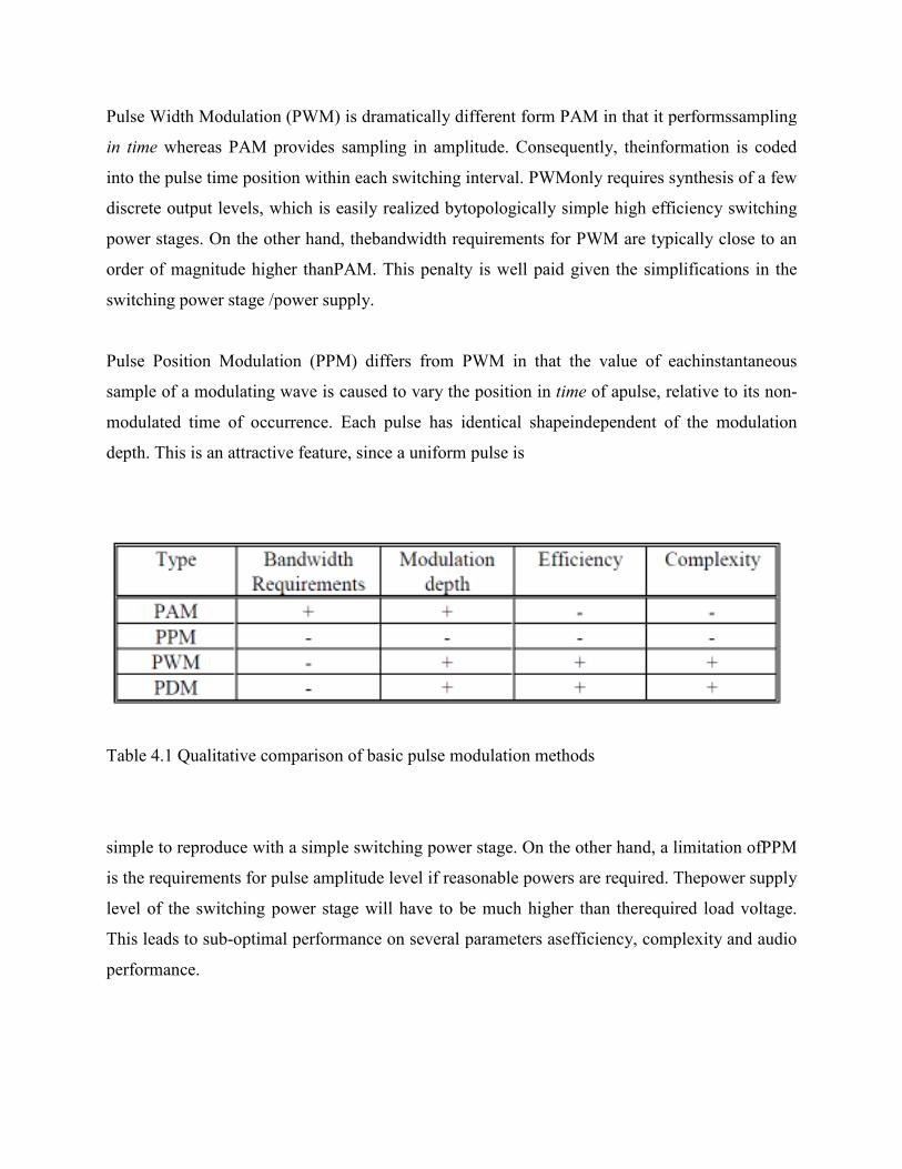
Pulse Width Modulation (PWM) is dramatically different form PAM in that it performssampling
in time whereas PAM provides sampling in amplitude. Consequently, theinformation is cod
into the pulse time position within each switching interval. PWMonly requires synthesis of a few
discrete output levels, which is easily realized bytopologically simple high efficiency switching
power stages. On the other hand, thebandwidth requirements
order of magnitude higher thanPAM. This penalty is well paid given the simplifications in the
switching power stage /power supply.
Pulse Position Modulation (PPM) differs from PWM in that the value of eachinstantaneous
sample of a modulating wave is caused to vary the position in
modulated time of occurrence. Each pulse has identical shapeindependent of the modulation
depth. This is an attractive feature, since a uniform pulse is
Table 4.1 Qualitative comparison of basic pulse modulation methods
simple to reproduce with a simple switching power stage. On the other hand, a limitation ofPPM
is the requirements for pulse amplitude level if reasonable powers are required. Thepower su
level of the switching power stage will have to be much higher than therequired load voltage.
This leads to sub-optimal performance on several parameters asefficiency, complexity and audio
performance.
Pulse Width Modulation (PWM) is dramatically different form PAM in that it performssampling
whereas PAM provides sampling in amplitude. Consequently, theinformation is cod
into the pulse time position within each switching interval. PWMonly requires synthesis of a few
discrete output levels, which is easily realized bytopologically simple high efficiency switching
power stages. On the other hand, thebandwidth requirements for PWM are typically close to an
order of magnitude higher thanPAM. This penalty is well paid given the simplifications in the
switching power stage /power supply.
Pulse Position Modulation (PPM) differs from PWM in that the value of eachinstantaneous
ample of a modulating wave is caused to vary the position in time of apulse, relative to its non
modulated time of occurrence. Each pulse has identical shapeindependent of the modulation
depth. This is an attractive feature, since a uniform pulse is
1 Qualitative comparison of basic pulse modulation methods
simple to reproduce with a simple switching power stage. On the other hand, a limitation ofPPM
is the requirements for pulse amplitude level if reasonable powers are required. Thepower su
level of the switching power stage will have to be much higher than therequired load voltage.
optimal performance on several parameters asefficiency, complexity and audio
Pulse Width Modulation (PWM) is dramatically different form PAM in that it performssampling
whereas PAM provides sampling in amplitude. Consequently, theinformation is coded
into the pulse time position within each switching interval. PWMonly requires synthesis of a few
discrete output levels, which is easily realized bytopologically simple high efficiency switching
for PWM are typically close to an
order of magnitude higher thanPAM. This penalty is well paid given the simplifications in the
Pulse Position Modulation (PPM) differs from PWM in that the value of eachinstantaneous
of apulse, relative to its non-
modulated time of occurrence. Each pulse has identical shapeindependent of the modulation
simple to reproduce with a simple switching power stage. On the other hand, a limitation ofPPM
is the requirements for pulse amplitude level if reasonable powers are required. Thepower supply
level of the switching power stage will have to be much higher than therequired load voltage.
optimal performance on several parameters asefficiency, complexity and audio
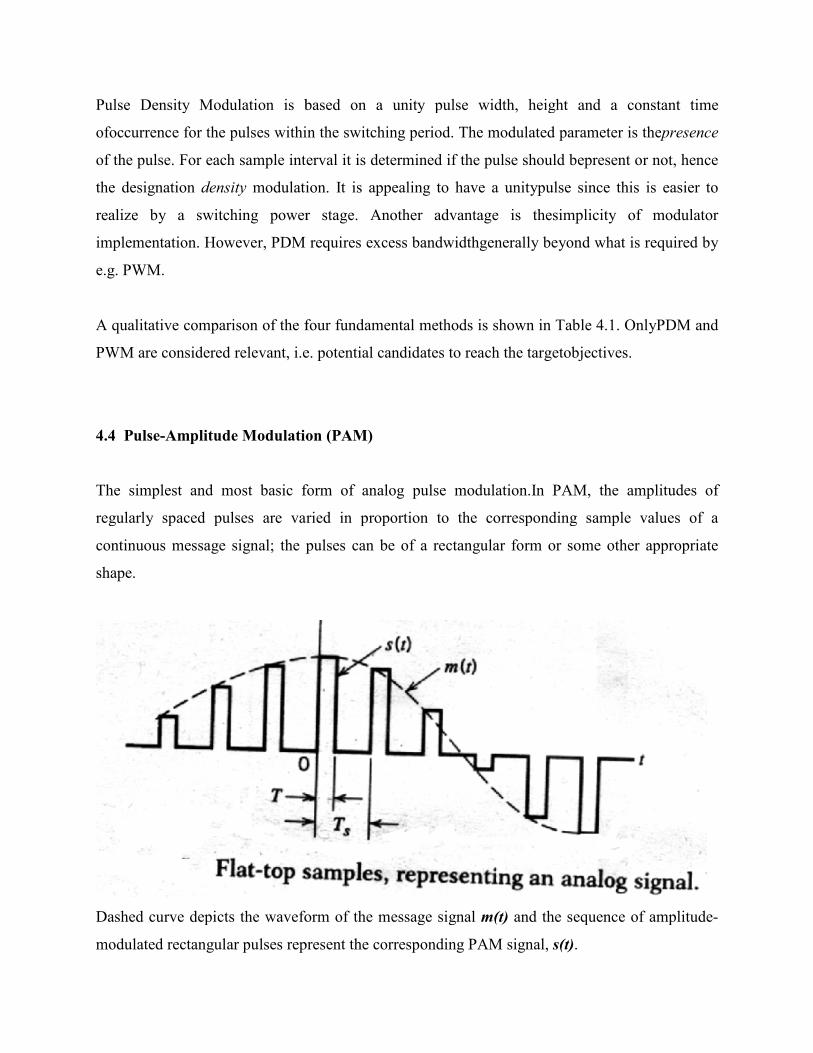
Pulse Density Modulation is based on a unity pul
ofoccurrence for the pulses within the switching period. The modulated parameter is the
of the pulse. For each sample interval it is determined if the pulse should bepresent or not, hence
the designation density modulation. It is appealing to have a unitypulse since this is easier to
realize by a switching power stage. Another advantage is thesimplicity of modulator
implementation. However, PDM requires excess bandwidthgenerally beyond what is required by
e.g. PWM.
A qualitative comparison of the four fundamental methods is shown in Table
PWM are considered relevant, i.e. potential candidates to reach the targetobjectives.
4.4 Pulse-Amplitude Modulation (PAM)
The simplest and most basic form
regularly spaced pulses are varied in proportion to the corresponding sample values of a
continuous message signal; the pulses can be of a rectangular form or some other appropriate
shape.
Dashed curve depicts the waveform of the message signal
modulated rectangular pulses represent the corresponding PAM signal,
Pulse Density Modulation is based on a unity pulse width, height and a constant time
ofoccurrence for the pulses within the switching period. The modulated parameter is the
of the pulse. For each sample interval it is determined if the pulse should bepresent or not, hence
modulation. It is appealing to have a unitypulse since this is easier to
realize by a switching power stage. Another advantage is thesimplicity of modulator
implementation. However, PDM requires excess bandwidthgenerally beyond what is required by
A qualitative comparison of the four fundamental methods is shown in Table 4.1. OnlyPDM and
PWM are considered relevant, i.e. potential candidates to reach the targetobjectives.
Amplitude Modulation (PAM)
The simplest and most basic form of analog pulse modulation.In PAM, the amplitudes of
regularly spaced pulses are varied in proportion to the corresponding sample values of a
continuous message signal; the pulses can be of a rectangular form or some other appropriate
ve depicts the waveform of the message signal m(t) and the sequence of amplitude
modulated rectangular pulses represent the corresponding PAM signal, s(t).
se width, height and a constant time
ofoccurrence for the pulses within the switching period. The modulated parameter is thepresence
of the pulse. For each sample interval it is determined if the pulse should bepresent or not, hence
modulation. It is appealing to have a unitypulse since this is easier to
realize by a switching power stage. Another advantage is thesimplicity of modulator
implementation. However, PDM requires excess bandwidthgenerally beyond what is required by
1. OnlyPDM and
PWM are considered relevant, i.e. potential candidates to reach the targetobjectives.
In PAM, the amplitudes of
regularly spaced pulses are varied in proportion to the corresponding sample values of a
continuous message signal; the pulses can be of a rectangular form or some other appropriate
and the sequence of amplitude-
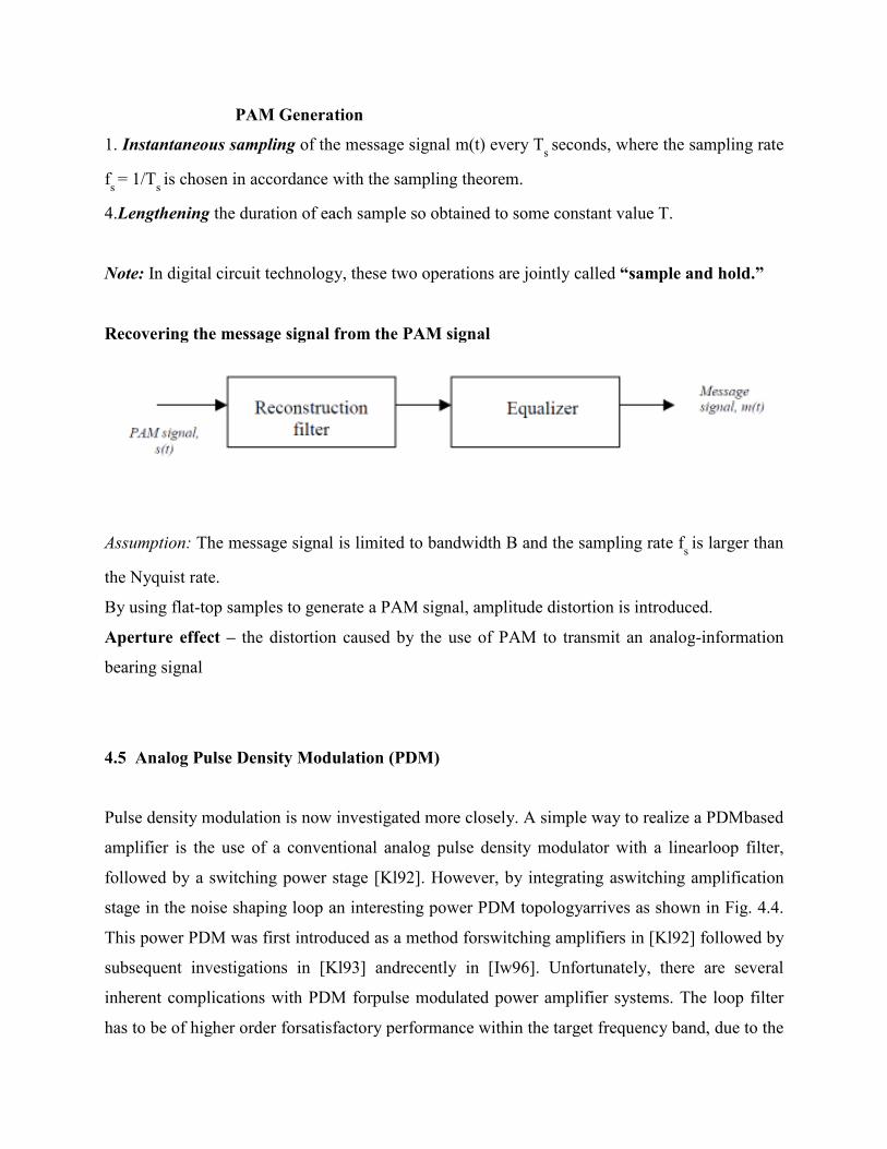
PAM Generation
1. Instantaneous sampling of the message signal m(t) every T
fs = 1/T
s is chosen in accordance with the sampling theorem.
4.Lengthening the duration of each sample so obtained to some constant value T.
Note: In digital circuit technology, these two operations are jointly called
Recovering the message signal from the PAM signal
Assumption: The message signal is limited to bandwidth B and the sampling rate f
the Nyquist rate.
By using flat-top samples to generate a PAM signal, amplitude distortion is introduced.
Aperture effect – the distortion caused by the use of PAM to transmit an analog
bearing signal
4.5 Analog Pulse Density Modulation (PDM)
Pulse density modulation is now investigated more closely. A simple way to realize a PDMbased
amplifier is the use of a conventional analog pulse density modulator with a linearloop filter,
followed by a switching power stage [Kl92]. However, by integrating aswitching a
stage in the noise shaping loop an interesting power PDM topologyarrives as shown in Fig.
This power PDM was first introduced as a method forswitching amplifiers in [Kl92] followed by
subsequent investigations in [Kl93] andrecently in [Iw96]. Unfortunately, there are several
inherent complications with PDM forpulse modulated power amplifier sy
has to be of higher order forsatisfactory performance within the target frequency band, due to the
PAM Generation
of the message signal m(t) every Ts seconds, where the sa
is chosen in accordance with the sampling theorem.
the duration of each sample so obtained to some constant value T.
In digital circuit technology, these two operations are jointly called “sample and hold.”
Recovering the message signal from the PAM signal
The message signal is limited to bandwidth B and the sampling rate f
top samples to generate a PAM signal, amplitude distortion is introduced.
the distortion caused by the use of PAM to transmit an analog
Analog Pulse Density Modulation (PDM)
modulation is now investigated more closely. A simple way to realize a PDMbased
amplifier is the use of a conventional analog pulse density modulator with a linearloop filter,
followed by a switching power stage [Kl92]. However, by integrating aswitching a
stage in the noise shaping loop an interesting power PDM topologyarrives as shown in Fig.
This power PDM was first introduced as a method forswitching amplifiers in [Kl92] followed by
subsequent investigations in [Kl93] andrecently in [Iw96]. Unfortunately, there are several
inherent complications with PDM forpulse modulated power amplifier systems. The loop filter
has to be of higher order forsatisfactory performance within the target frequency band, due to the
seconds, where the sampling rate
the duration of each sample so obtained to some constant value T.
“sample and hold.”
The message signal is limited to bandwidth B and the sampling rate fs is larger than
top samples to generate a PAM signal, amplitude distortion is introduced.
the distortion caused by the use of PAM to transmit an analog-information
modulation is now investigated more closely. A simple way to realize a PDMbased
amplifier is the use of a conventional analog pulse density modulator with a linearloop filter,
followed by a switching power stage [Kl92]. However, by integrating aswitching amplification
stage in the noise shaping loop an interesting power PDM topologyarrives as shown in Fig. 4.4.
This power PDM was first introduced as a method forswitching amplifiers in [Kl92] followed by
subsequent investigations in [Kl93] andrecently in [Iw96]. Unfortunately, there are several
stems. The loop filter
has to be of higher order forsatisfactory performance within the target frequency band, due to the
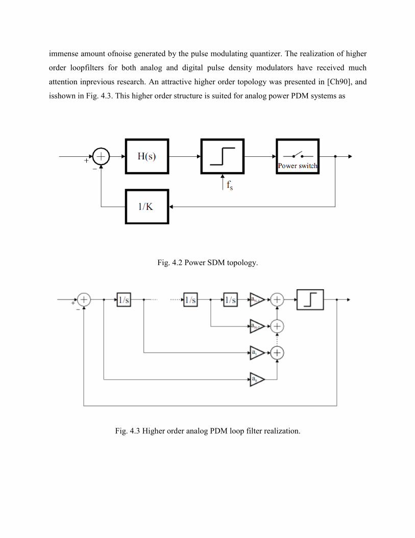
immense amount ofnoise generated by the pulse modulating quantizer. The realization of higher
order loopfilters for both analog and di
attention inprevious research. An attractive higher order topology was presented in [Ch90], and
isshown in Fig. 4.3. This higher order structure is suited for analog power PDM systems as
Fig. 4.3 Higher order analog PDM loop filter realization.
immense amount ofnoise generated by the pulse modulating quantizer. The realization of higher
order loopfilters for both analog and digital pulse density modulators have received much
attention inprevious research. An attractive higher order topology was presented in [Ch90], and
3. This higher order structure is suited for analog power PDM systems as
Fig. 4.2 Power SDM topology.
3 Higher order analog PDM loop filter realization.
immense amount ofnoise generated by the pulse modulating quantizer. The realization of higher
gital pulse density modulators have received much
attention inprevious research. An attractive higher order topology was presented in [Ch90], and
3. This higher order structure is suited for analog power PDM systems as
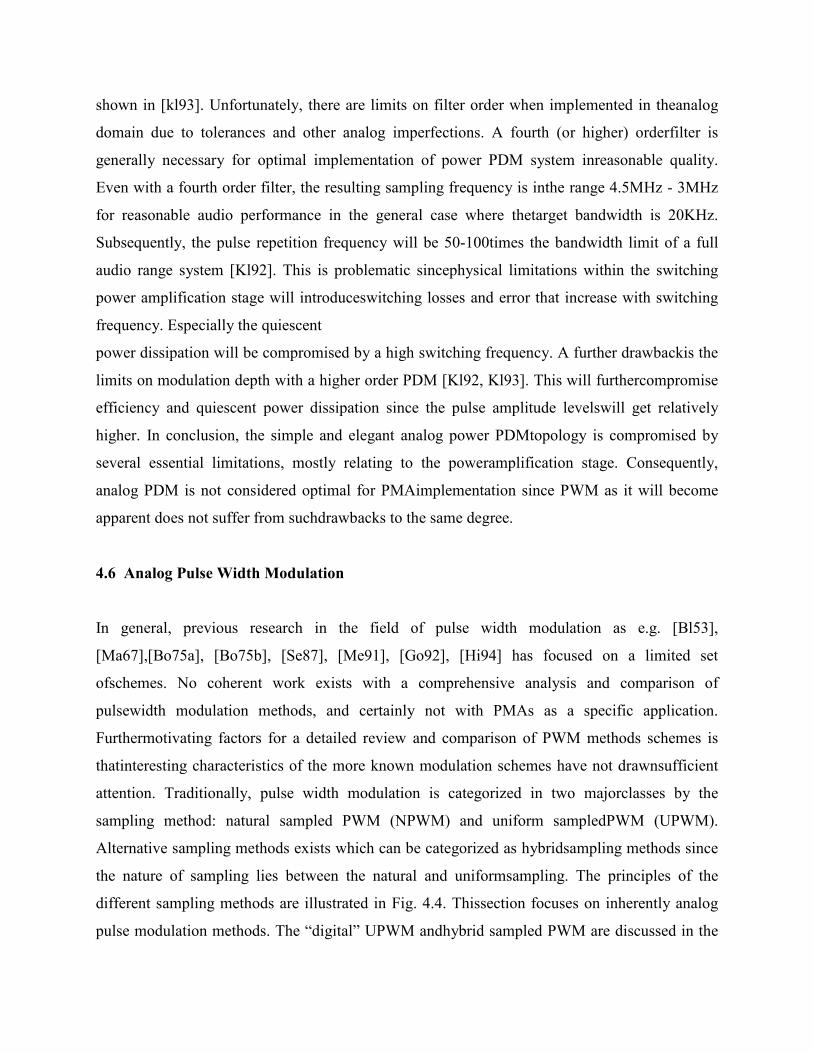
shown in [kl93]. Unfortunately, there are limits on filter order when implemented in theanalog
domain due to tolerances and other analog imperfections. A fourth (or higher) orderfilter is
generally necessary for optimal implementation of power PDM system inreasonable quality.
Even with a fourth order filter, the resulting sampling frequency is inthe range 4.5MHz - 3MHz
for reasonable audio performance in the general case where thetarget bandwidth is 20KHz.
Subsequently, the pulse repetition frequency will be 50-100times the bandwidth limit of a full
audio range system [Kl92]. This is problematic sincephysical limitations within the switching
power amplification stage will introduceswitching losses and error that increase with switching
frequency. Especially the quiescent
power dissipation will be compromised by a high switching frequency. A further drawbackis the
limits on modulation depth with a higher order PDM [Kl92, Kl93]. This will furthercompromise
efficiency and quiescent power dissipation since the pulse amplitude levelswill get relatively
higher. In conclusion, the simple and elegant analog power PDMtopology is compromised by
several essential limitations, mostly relating to the poweramplification stage. Consequently,
analog PDM is not considered optimal for PMAimplementation since PWM as it will become
apparent does not suffer from suchdrawbacks to the same degree.
4.6 Analog Pulse Width Modulation
In general, previous research in the field of pulse width modulation as e.g. [Bl53],
[Ma67],[Bo75a], [Bo75b], [Se87], [Me91], [Go92], [Hi94] has focused on a limited set
ofschemes. No coherent work exists with a comprehensive analysis and comparison of
pulsewidth modulation methods, and certainly not with PMAs as a specific application.
Furthermotivating factors for a detailed review and comparison of PWM methods schemes is
thatinteresting characteristics of the more known modulation schemes have not drawnsufficient
attention. Traditionally, pulse width modulation is categorized in two majorclasses by the
sampling method: natural sampled PWM (NPWM) and uniform sampledPWM (UPWM).
Alternative sampling methods exists which can be categorized as hybridsampling methods since
the nature of sampling lies between the natural and uniformsampling. The principles of the
different sampling methods are illustrated in Fig. 4.4. Thissection focuses on inherently analog
pulse modulation methods. The “digital” UPWM andhybrid sampled PWM are discussed in the
next chapter. Besides the sampling method,PWM is traditionally also differentiated by the edge
modulation and by the class. The edgemodulation may be single sided or double sided. The
modulation of both edges doubles theinformation stored in the resulting pulse train, although the
pulse train frequency is thesame. Class AD and Class BD are the (somewhat misleading but
standardized)
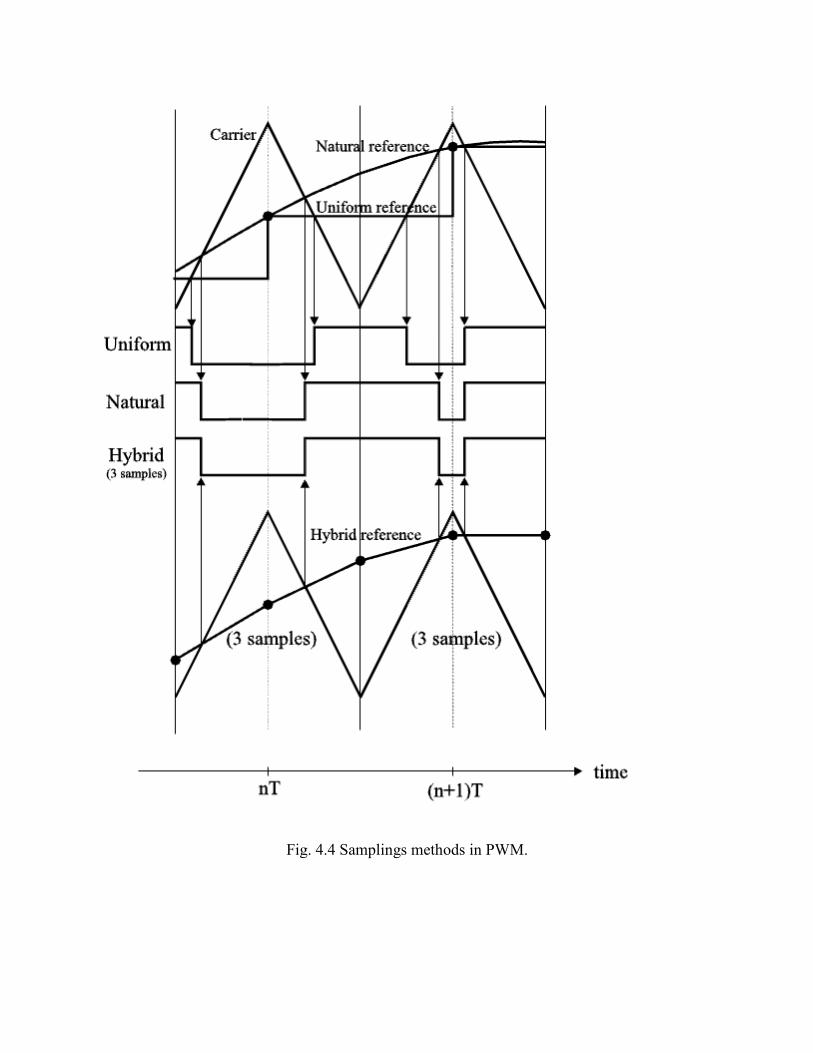
Fig.
Fig. 4.4 Samplings methods in PWM.
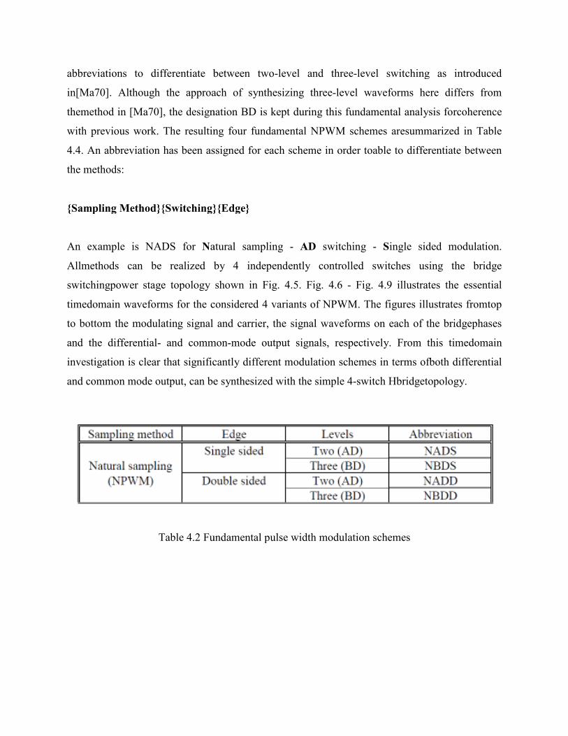
abbreviations to differentiate between two
in[Ma70]. Although the approach of synthesizing three
themethod in [Ma70], the designation BD is kept during this fundamental analysis forcoherence
with previous work. The resulting four fundamental NPWM schemes aresummarized in Table
4.4. An abbreviation has been assigned for each scheme i
the methods:
Sampling MethodSwitchingEdge
An example is NADS for Natural sampling
Allmethods can be realized by 4 independently controlled switches using the bridge
switchingpower stage topology shown in Fig.
timedomain waveforms for the considered 4 variants of
to bottom the modulating signal and carrier, the signal waveforms on each of the bridgephases
and the differential- and common
investigation is clear that significantly different modulation schemes in terms ofboth differential
and common mode output, can be synthesized with the simple 4
Table 4.2 Fundamental pulse width modulation schemes
abbreviations to differentiate between two-level and three-level switching as introduced
in[Ma70]. Although the approach of synthesizing three-level waveforms here differs from
themethod in [Ma70], the designation BD is kept during this fundamental analysis forcoherence
with previous work. The resulting four fundamental NPWM schemes aresummarized in Table
An abbreviation has been assigned for each scheme in order toable to differentiate between
Sampling MethodSwitchingEdge
atural sampling - AD switching - Single sided modulation.
Allmethods can be realized by 4 independently controlled switches using the bridge
switchingpower stage topology shown in Fig. 4.5. Fig. 4.6 - Fig. 4.9 illustrates the essential
timedomain waveforms for the considered 4 variants of NPWM. The figures illustrates fromtop
to bottom the modulating signal and carrier, the signal waveforms on each of the bridgephases
and common-mode output signals, respectively. From this timedomain
cantly different modulation schemes in terms ofboth differential
and common mode output, can be synthesized with the simple 4-switch Hbridgetopology.
2 Fundamental pulse width modulation schemes
level switching as introduced
here differs from
themethod in [Ma70], the designation BD is kept during this fundamental analysis forcoherence
with previous work. The resulting four fundamental NPWM schemes aresummarized in Table
n order toable to differentiate between
ingle sided modulation.
Allmethods can be realized by 4 independently controlled switches using the bridge
9 illustrates the essential
NPWM. The figures illustrates fromtop
to bottom the modulating signal and carrier, the signal waveforms on each of the bridgephases
mode output signals, respectively. From this timedomain
cantly different modulation schemes in terms ofboth differential
switch Hbridgetopology.
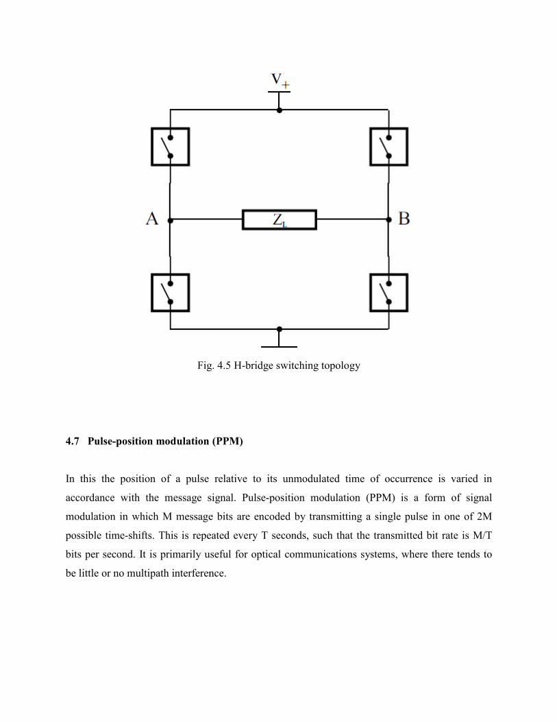
Fig.
4.7 Pulse-position modulation (PPM)
In this the position of a pulse relative to its unmodulated time of occurrence is varied in
accordance with the message signal. Pulse
modulation in which M message bits are encoded by transmitting a single pulse in one of 2M
possible time-shifts. This is repeated every T seconds, such that the transmitted bit rate is M/T
bits per second. It is primarily useful for
be little or no multipath interference.
Fig. 4.5 H-bridge switching topology
position modulation (PPM)
In this the position of a pulse relative to its unmodulated time of occurrence is varied in
accordance with the message signal. Pulse-position modulation (PPM) is a form of signal
in which M message bits are encoded by transmitting a single pulse in one of 2M
shifts. This is repeated every T seconds, such that the transmitted bit rate is M/T
bits per second. It is primarily useful for optical communications systems, where there tends to
interference.
In this the position of a pulse relative to its unmodulated time of occurrence is varied in
position modulation (PPM) is a form of signal
in which M message bits are encoded by transmitting a single pulse in one of 2M
shifts. This is repeated every T seconds, such that the transmitted bit rate is M/T
systems, where there tends to
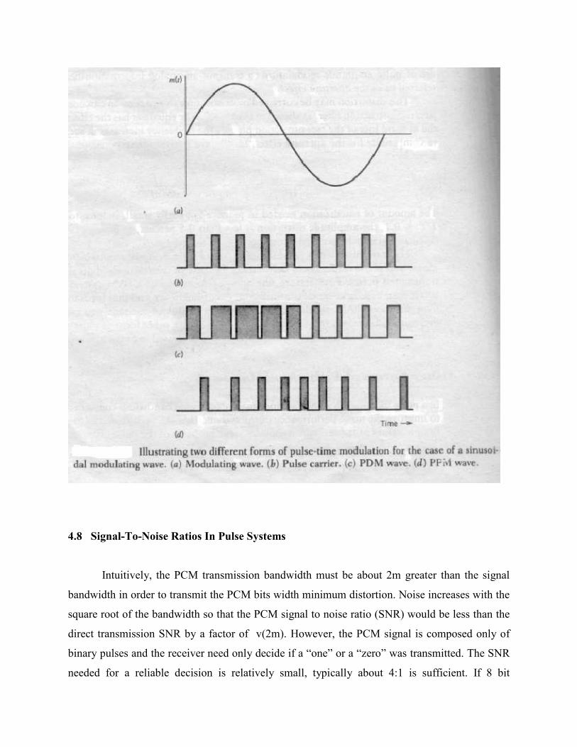
4.8 Signal-To-Noise Ratios In Pulse Systems
Intuitively, the PCM transmission bandwidth must be about 2m greater than the signal
bandwidth in order to transmit the PCM bits width minimum distortion. Noise increases with the
square root of the bandwidth so that the PCM signal to noise ratio (SNR) would be less than the
direct transmission SNR by a factor of v(2m). However, the PCM signal is composed only of
binary pulses and the receiver need only decide if a “one” or a “zero” was transmitted. The SNR
needed for a reliable decision is relatively small, typically about 4:1 is sufficient. If 8 bit
quantization were used, a direct transmission channel SNR of greater than 100:1 would be
required to maintain the 8 bit signal precision. Using PCM, a band width increase of about 16:1
would be required, increasing the transmission noise by about 4:1, however , a channel SNR of
only 4:1 or 5:1 would be required. Thus, the PCM transmission would require about a 20:1 SNR
defined in a bandwidth equal to the signal bandwidth for the PCM system compared to over
100:1 SNR for direct transmission. Thus PCM has exchanged bandwidth for signal to noise ratio.
In 1959, C.E. Shannon published a key development in communications theory in which he
propsed a theoretical bound for communication over a noisy analog channel. Shannon developed
the channel capacity bound:
C=W log 2 (1+ SNR )
Where C= the channel capacity in bits per second, W= the channel bandwidth in Herts, and SNR
= the channel signal to noise ratio.
Shannon’s bound is very interesting because it asserts that there exist coding schemes
which will allow the channel capacity to be reached with arbitrarily small error rate. Further
theorem suggests that capacity can be traded for signal to noise ratio.
4.9 Summary
A comprehensive investigation of analog pulse modulation methods has been carried
outwith the primary motivation to devise optimal modulation strategies for PMA systems.This
has involved a fundamental analysis and comparison of known methods followed
byinvestigations of new enhanced pulse modulation methods with improved characteristics.An
initial investigation of PAM, PPM, PWM and PDM concluded on the advantages ofPWM.
Following, the tonal behavior of the four fundamental NPWM schemes wasanalyzed by
developing DFS expressions for the differential and common modecomponents of the modulated
output.
4.10 Keywords
PAM
PPM
PWM
PDM
4.11 Exercise
1. Explain Analog Pulse Density Modulation (PDM).
2. Explain Analog Pulse Width Modulation.
3. Define PPM.
.
Unit 1
DM and PCM
Structure
1.1 Introduction
1.2 Objectives
1.3 Delta modulation and DPCM
1.4 Pulse-Code Modulation
1.5 Comparison of PCM and DM
1.6 Summary
1.7 Keywords
1.8 Exercise
1.1 Introduction
In electronics, modulation is the process of varying one or more properties of a high-
frequency periodic waveform, called the carrier signal, with a modulating signal which typically
contains information to be transmitted. This is done in a similar fashion to
a musician modulating a tone (a periodic waveform) from a musical instrument by varying
its volume, timing and pitch. The three key parameters of a periodic waveform are
its amplitude ("volume"), its phase ("timing") and its frequency ("pitch"). Any of these properties
can be modified in accordance with a low frequency signal to obtain the modulated signal.
Typically a high-frequencysinusoid waveform is used as carrier signal, but a square wave pulse
train may also be used.
In telecommunications, modulation is the process of conveying a message signal, for
example a digital bit stream or an analog audio signal, inside another signal that can be
physically transmitted. Modulation of a sine waveform is used to transform a baseband message
signal into a pass band signal, for example low-frequency audio signal into a radio-frequency
signal (RF signal). In radio communications, cable TV systems or the public switched telephone
network for instance, electrical signals can only be transferred over a limited pass band
frequency spectrum, with specific (non-zero) lower and upper cutoff frequencies. Modulating a
sine-wave carrier makes it possible to keep the frequency content of the transferred signal as
close as possible to the centre frequency (typically the carrier frequency) of the pass band.
1.2 Objectives
At the end of this chapter you will be able to:
• Explain Delta modulation and DPCM.
• Define PCM.
• Give the Comparison of PCM and DM.
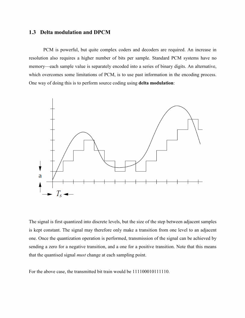
1.3 Delta modulation and DPCM
PCM is powerful, but quite complex coders and decoders are
resolution also requires a higher number of bits per sample.
memory—each sample value is separately
which overcomes some limitations of
One way of doing this is to perform source coding using
The signal is first quantized into discrete levels, but the size of the step between
is kept constant. The signal may therefore only make a
one. Once the quantization operation is
sending a zero for a negative transition, and a one for a positive transition. Note that thi
that the quantised signal must change at each sampling point.
For the above case, the transmitted bit train would be 111100010111110.
Delta modulation and DPCM
PCM is powerful, but quite complex coders and decoders are required. An increase in
resolution also requires a higher number of bits per sample. Standard PCM systems have no
each sample value is separately encoded into a series of binary digits. An alternative,
limitations of PCM, is to use past information in the encoding process.
way of doing this is to perform source coding using delta modulation:
into discrete levels, but the size of the step between adjacent samples
may therefore only make a transition from one level to an adjacent
operation is performed, transmission of the signal can be achieved by
negative transition, and a one for a positive transition. Note that thi
change at each sampling point.
For the above case, the transmitted bit train would be 111100010111110.
required. An increase in
Standard PCM systems have no
encoded into a series of binary digits. An alternative,
use past information in the encoding process.
adjacent samples
transition from one level to an adjacent
performed, transmission of the signal can be achieved by
negative transition, and a one for a positive transition. Note that this means
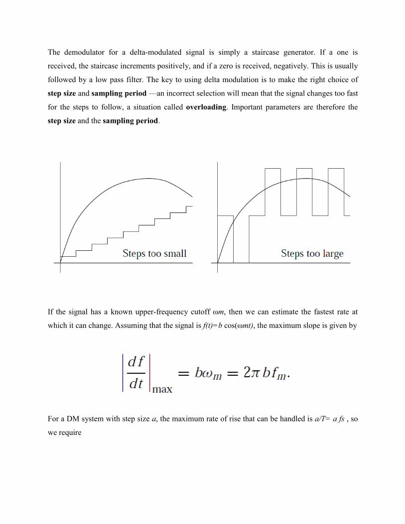
The demodulator for a delta-modulated signal is simply a staircase generator.
received, the staircase increments positively, and if a zero is
followed by a low pass filter. The key to using delta modulation is to make the right choice of
step size and sampling period —
for the steps to follow, a situation called
step size and the sampling period
If the signal has a known upper
which it can change. Assuming that the signal is
For a DM system with step size a
we require
modulated signal is simply a staircase generator.
increments positively, and if a zero is received, negatively. This is usually
The key to using delta modulation is to make the right choice of
—an incorrect selection will mean that the signal c
for the steps to follow, a situation called overloading. Important parameters are therefore the
sampling period.
If the signal has a known upper-frequency cutoff ωm, then we can estimate the
can change. Assuming that the signal is f(t)=b cos(ωmt), the maximum slope is given by
a, the maximum rate of rise that can be handled is
modulated signal is simply a staircase generator. If a one is
received, negatively. This is usually
The key to using delta modulation is to make the right choice of
an incorrect selection will mean that the signal changes too fast
parameters are therefore the
, then we can estimate the fastest rate at
, the maximum slope is given by
handled is a/T= a fs , so
Making the assumption that the quantisation noise in
mean-square quantisation error power is
all frequencies up to the sampling frequency
DM receiver —if the cutoff frequency is set to the maximum frequency
power in the reconstructed signal is
Still making the assumption of a sinusoidal signal, the SNR for DM is
when the slope overload condition is just met. The SNR therefore increases by 9dB for every
doubling of the sampling frequency.
Delta modulation is extremely simple, and gives
but is clearly limited. One way of attempting to improve
where the step size is not required to be
space shuttles make use of this te
size is encoded as a (multiple bit) PCM signal, and transmitted to the receiver
Differential PCM is similar, but encodes the difference between
—this can further reduce the number of bits
Making the assumption that the quantisation noise in DM is uniformly distributed over(
square quantisation error power is a2/3. We assume that this power is spread evenly over
sampling frequency fs . However, there is still the low pass
the cutoff frequency is set to the maximum frequency fm, then
power in the reconstructed signal is
Still making the assumption of a sinusoidal signal, the SNR for DM is
the slope overload condition is just met. The SNR therefore increases by 9dB for every
doubling of the sampling frequency.
Delta modulation is extremely simple, and gives acceptable performance in many applications,
but is clearly limited. One way of attempting to improve performance is to use
where the step size is not required to be constant. (The voice communication systems on the US
use of this technique.) Another is to use delta PCM, where each desired step
size is encoded as a (multiple bit) PCM signal, and transmitted to the receiver
Differential PCM is similar, but encodes the difference between a sample and its
this can further reduce the number of bits required for transmission.
distributed over(-a, a), the
We assume that this power is spread evenly over
low pass filter in the
, then the total noise
the slope overload condition is just met. The SNR therefore increases by 9dB for every
performance in many applications,
performance is to use adaptive DM,
constant. (The voice communication systems on the US
chnique.) Another is to use delta PCM, where each desired step
size is encoded as a (multiple bit) PCM signal, and transmitted to the receiver as a codeword.
a sample and its predicted value
2.4 Pulse-Code Modulation
PULSE-CODE MODULATION (PCM) refers to a system in which the standard values
of a QUANTIZED WAVE (explained in the following paragraphs) are indicated by a series of
coded pulses. When these pulses are decoded, they indicate the standard values of the original
quantized wave. These codes may be binary, in which the symbol for each quantized element
will consist of pulses and spaces: ternary, where the code for each element consists of any one of
three distinct kinds of values (such as positive pulses, negative pulses, and spaces); or n-ary, in
which the code for each element consists of nay number (n) of distinct values. This discussion
will be based on the binary PCM system. All of the pulse-modulation systems discussed
previously provides methods of converting analog wave shapes to digital wave shapes (pulses
occurring at discrete intervals, some characteristic of which is varied as a continuous function of
the analog wave). The entire range of amplitude (frequency or phase) values of the analog wave
can be arbitrarily divided into a series of standard values. Each pulse of a pulse train [figure 2-
48, view (B)] takes the standard value nearest its actual value when modulated. The modulating
wave can be faithfully reproduced, as shown in views (C) and (D). The amplitude range has been
divided into 5 standard values in view (C). Each pulse is given whatever standard value is
nearest its actual instantaneous value. In view (D), the same amplitude range has been divided
into 10 standard levels. The curve of view (D) is a much closer approximation of the modulating
wave, view (A), than is the 5-level quantized curve in view (C). From this you should see that
the greater the number of standard levels used, the more closely the quantized wave
approximates the original. This is also made evident by the fact that an infinite number of
standard levels exactly duplicate the conditions of non-quantization (the original analog
waveform).
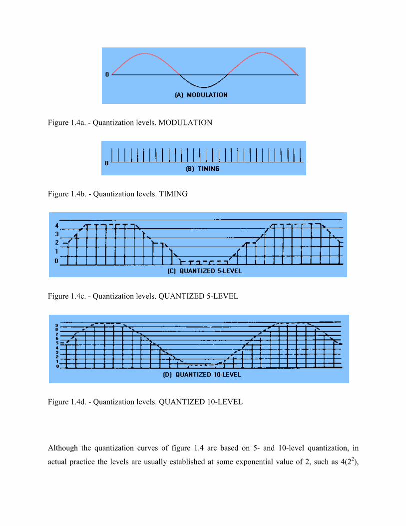
Figure 1.4a. - Quantization levels. MODULATION
Figure 1.4b. - Quantization levels. TIMING
Figure 1.4c. - Quantization levels. QUANTIZED 5-LEVEL
Figure 1.4d. - Quantization levels. QUANTIZED 10-LEVEL
Although the quantization curves of figure 1.4 are based on 5- and 10-level quantization, in
actual practice the levels are usually established at some exponential value of 2, such as 4(22),
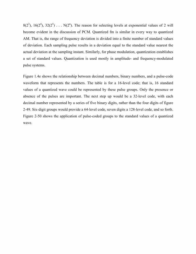
8(23), 16(2
4), 32(2
5) . . . N(2
n). The reason for selecting levels at exponential values of 2 will
become evident in the discussion of PCM. Quantized fm is similar in every way to quantized
AM. That is, the range of frequency deviation is divided into a finite number of standard values
of deviation. Each sampling pulse results in a deviation equal to the standard value nearest the
actual deviation at the sampling instant. Similarly, for phase modulation, quantization establishes
a set of standard values. Quantization is used mostly in amplitude- and frequency-modulated
pulse systems.
Figure 1.4e shows the relationship between decimal numbers, binary numbers, and a pulse-code
waveform that represents the numbers. The table is for a 16-level code; that is, 16 standard
values of a quantized wave could be represented by these pulse groups. Only the presence or
absence of the pulses are important. The next step up would be a 32-level code, with each
decimal number represented by a series of five binary digits, rather than the four digits of figure
2-49. Six-digit groups would provide a 64-level code, seven digits a 128-level code, and so forth.
Figure 2-50 shows the application of pulse-coded groups to the standard values of a quantized
wave.
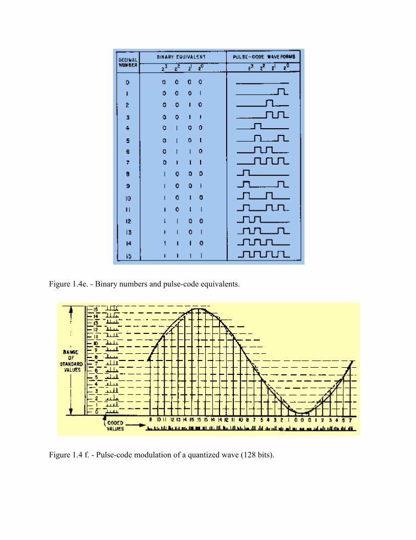
Figure 1.4e. - Binary numbers and pulse-code equivalents.
Figure 1.4 f. - Pulse-code modulation of a quantized wave (128 bits).
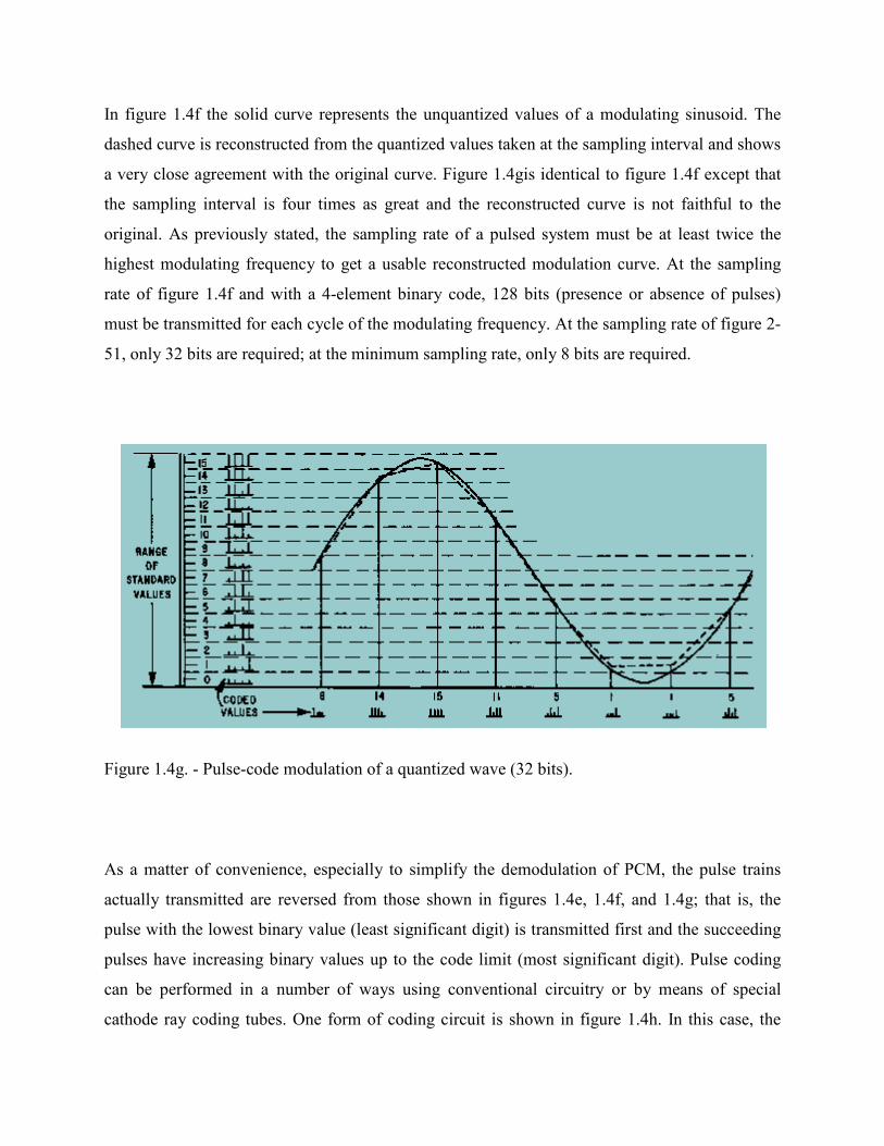
In figure 1.4f the solid curve represents the unquantized values of a modulating sinusoid. The
dashed curve is reconstructed from the quantized values taken at the sampling interval and shows
a very close agreement with the original curve. Figure 1.4gis identical to figure 1.4f except that
the sampling interval is four times as great and the reconstructed curve is not faithful to the
original. As previously stated, the sampling rate of a pulsed system must be at least twice the
highest modulating frequency to get a usable reconstructed modulation curve. At the sampling
rate of figure 1.4f and with a 4-element binary code, 128 bits (presence or absence of pulses)
must be transmitted for each cycle of the modulating frequency. At the sampling rate of figure 2-
51, only 32 bits are required; at the minimum sampling rate, only 8 bits are required.
Figure 1.4g. - Pulse-code modulation of a quantized wave (32 bits).
As a matter of convenience, especially to simplify the demodulation of PCM, the pulse trains
actually transmitted are reversed from those shown in figures 1.4e, 1.4f, and 1.4g; that is, the
pulse with the lowest binary value (least significant digit) is transmitted first and the succeeding
pulses have increasing binary values up to the code limit (most significant digit). Pulse coding
can be performed in a number of ways using conventional circuitry or by means of special
cathode ray coding tubes. One form of coding circuit is shown in figure 1.4h. In this case, the
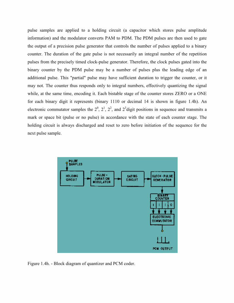
pulse samples are applied to a holding circuit (a capacitor which stores pulse amplitude
information) and the modulator converts PAM to PDM. The PDM pulses are then used to gate
the output of a precision pulse generator that controls the number of pulses applied to a binary
counter. The duration of the gate pulse is not necessarily an integral number of the repetition
pulses from the precisely timed clock-pulse generator. Therefore, the clock pulses gated into the
binary counter by the PDM pulse may be a number of pulses plus the leading edge of an
additional pulse. This "partial" pulse may have sufficient duration to trigger the counter, or it
may not. The counter thus responds only to integral numbers, effectively quantizing the signal
while, at the same time, encoding it. Each bistable stage of the counter stores ZERO or a ONE
for each binary digit it represents (binary 1110 or decimal 14 is shown in figure 1.4h). An
electronic commutator samples the 20, 2
1, 2
2, and 2
3digit positions in sequence and transmits a
mark or space bit (pulse or no pulse) in accordance with the state of each counter stage. The
holding circuit is always discharged and reset to zero before initiation of the sequence for the
next pulse sample.
Figure 1.4h. - Block diagram of quantizer and PCM coder.
The PCM demodulator will reproduce the correct standard amplitude represented by the pulse-
code group. However, it will reproduce the correct standard only if it is able to recognize
correctly the presence or absence of pulses in each position. For this reason, noise introduces no
error at all if the signal-to-noise ratio is such that the largest peaks of noise are not mistaken for
pulses. When the noise is random (circuit and tube noise), the probability of the appearance of a
noise peak comparable in amplitude to the pulses can be determined. This probability can be
determined mathematically for any ration of signal-to-average-noise power. When this is done
for 105 pulses per second, the approximate error rate for three values of signal power to average
noise power is:
17 dB - 10 errors per second
20 dB - 1 error every 20 minutes
22 dB - 1 error every 2,000 hours
Above a threshold of signal-to-noise ration of approximately 20 dB, virtually no errors occur. In
all other systems of modulation, even with signal-to-noise ratios as high as 60 dB, the noise will
have some effect. Moreover, the PCM signal can be retransmitted, as in a multiple relay link
system, as many times as desired, without the introduction of additional noise effects; that is,
noise is not cumulative at relay stations as it is with other modulation systems.
The system does, of course, have some distortion introduced by quantizing the signal. Both the
standard values selected and the sampling interval tends to make the reconstructed wave depart
from the original. This distortion, called QUANTIZING NOISE, is initially introduced at the
quantizing and coding modulator and remains fixed throughout the transmission and
retransmission processes. Its magnitude can be reduced by making the standard quantizing levels
closer together. The relationship of the quantizing noise to the number of digits in the binary
code is given by the following standard relationship:
Where:
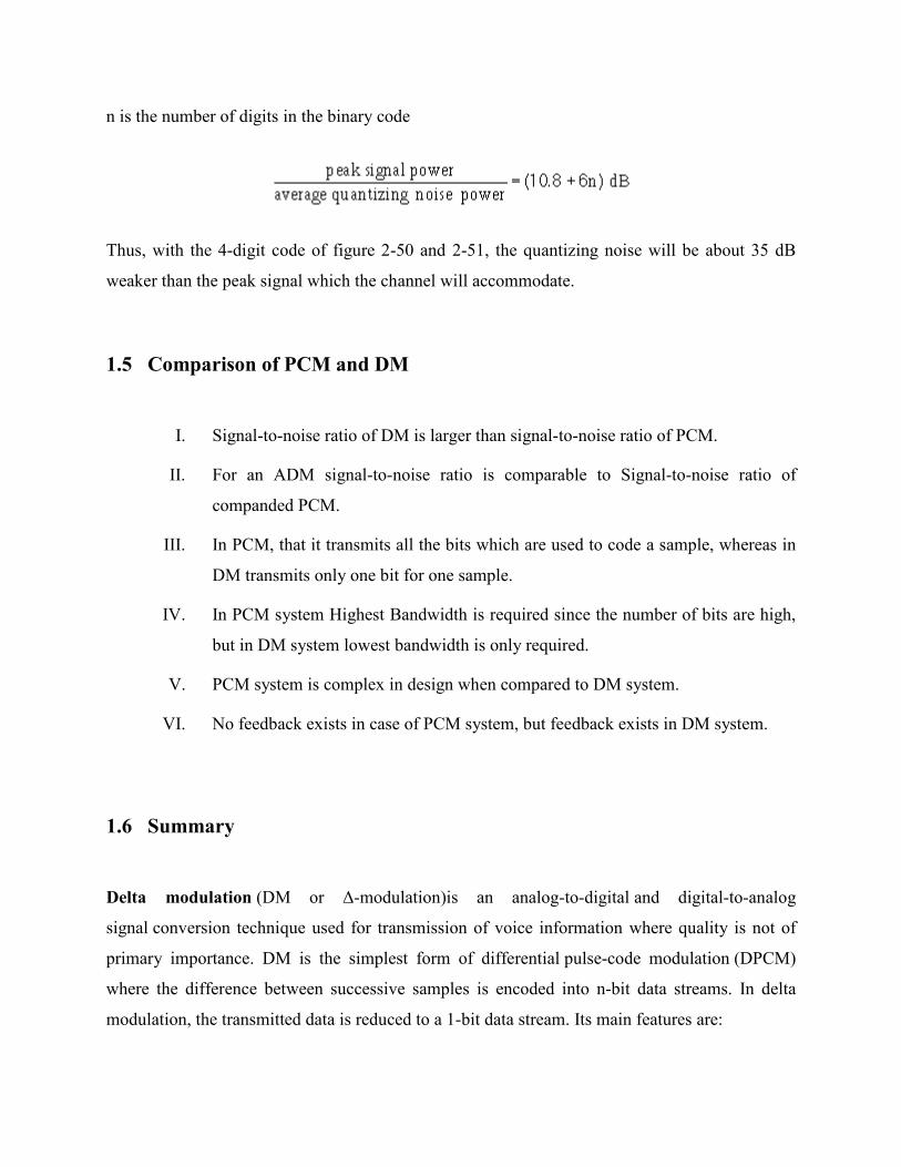
n is the number of digits in the binary code
Thus, with the 4-digit code of figure 2-50 and 2-51, the quantizing noise will be about 35 dB
weaker than the peak signal which the channel will accommodate.
1.5 Comparison of PCM and DM
I. Signal-to-noise ratio of DM is larger than signal-to-noise ratio of PCM.
II. For an ADM signal-to-noise ratio is comparable to Signal-to-noise ratio of
companded PCM.
III. In PCM, that it transmits all the bits which are used to code a sample, whereas in
DM transmits only one bit for one sample.
IV. In PCM system Highest Bandwidth is required since the number of bits are high,
but in DM system lowest bandwidth is only required.
V. PCM system is complex in design when compared to DM system.
VI. No feedback exists in case of PCM system, but feedback exists in DM system.
1.6 Summary
Delta modulation (DM or ∆-modulation)is an analog-to-digital and digital-to-analog
signal conversion technique used for transmission of voice information where quality is not of
primary importance. DM is the simplest form of differential pulse-code modulation (DPCM)
where the difference between successive samples is encoded into n-bit data streams. In delta
modulation, the transmitted data is reduced to a 1-bit data stream. Its main features are:
the analog signal is approximated with a series of segments
each segment of the approximated signal is compared to the original analog wave to
determine the increase or decrease in relative amplitude
the decision process for establishing the state of successive bits is determined by this
comparison
only the change of information is sent, that is, only an increase or decrease of the signal
amplitude from the previous sample is sent whereas a no-change condition causes the
modulated signal to remain at the same 0 or 1 state of the previous sample.
The advantages of PCM are two-fold. First, noise interference is almost completely
eliminated when the pulse signals exceed noise levels by a value of 20 dB or more. Second, the
signal may be received and retransmitted as many times as may be desired without introducing
distortion into the signal.
1.7 Keywords
• DM
• PCM
• DPCM
• Carrier signal,
• Modulating signal
• Sampling period
1.8 Exercise
1) Pulse-code modulation requires the use of approximations of value that are obtained by
what process?
2) If a modulating wave is sampled 10 times per cycle with a 5-element binary code, how
many bits of information are required to transmit the signal?
3) What is the primary advantage of pulse-modulation systems?
4) Give the comparison between PCM and DM.
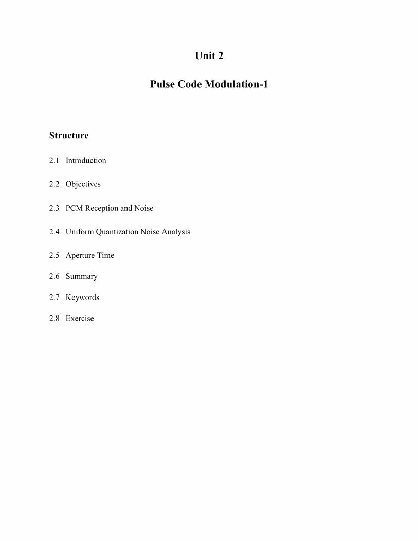
Unit 2
Pulse Code Modulation-1
Structure
2.1 Introduction
2.2 Objectives
2.3 PCM Reception and Noise
2.4 Uniform Quantization Noise Analysis
2.5 Aperture Time
2.6 Summary
2.7 Keywords
2.8 Exercise
2.1 Introduction
PCM is a term which was formed during the development of digital audio transmission
standards. Digital data can be transported robustly over long distances unlike the analog data and
can be interleaved with other digital data so various combinations of transmission channels can
be used. In the text which follows this term will apply to encoding technique which means
digitalization of analog information in general. In this we go through the Uniform Quantization
Noise Analysis.
2.2 Objectives
At the end of this chapter you will be able to:
• Know PCM Reception And Noise
• Explain Uniform Quantization Noise Analysis
• Define Aperture Time
2.3 PCM Reception And Noise
PCM is a method of converting an analog into digital signals. Information in an analog
form cannot be processed by digital computers so it's necessary to convert them into digital form.
PCM is a term which was formed during the development of digital audio transmission
standards. Digital data can be transported robustly over long distances unlike the analog data and
can be interleaved with other digital data so various combinations of transmission channels can
be used. In the text which follows this term will apply to encoding technique which means
digitalization of analog information in general.
PCM doesn`t mean any specific kind of compression, it only implies PAM (pulse
amplitude modulation) - quantization by amplitude and quantization by time which means
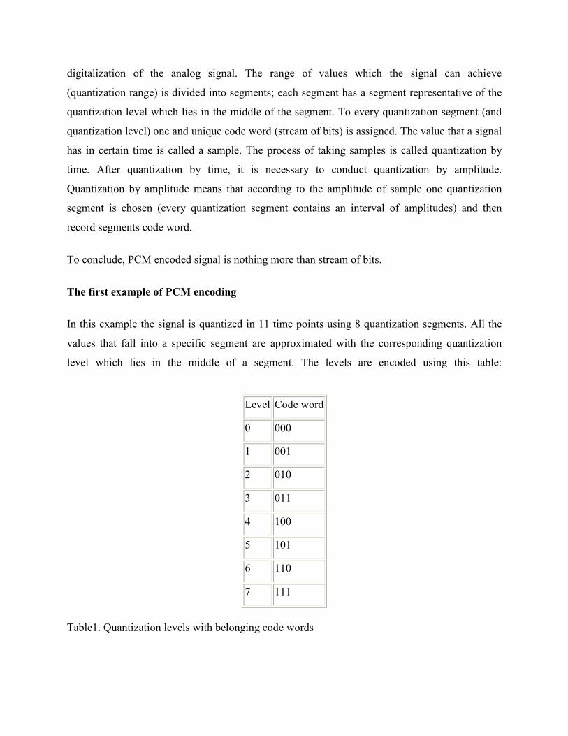
digitalization of the analog signal. The range of values which the signal can achieve
(quantization range) is divided into segments; each segment has a segment representative of the
quantization level which lies in the middle of the segment. To every quantization segment (and
quantization level) one and unique code word (stream of bits) is assigned. The value that a signal
has in certain time is called a sample. The process of taking samples is called quantization by
time. After quantization by time, it is necessary to conduct quantization by amplitude.
Quantization by amplitude means that according to the amplitude of sample one quantization
segment is chosen (every quantization segment contains an interval of amplitudes) and then
record segments code word.
To conclude, PCM encoded signal is nothing more than stream of bits.
The first example of PCM encoding
In this example the signal is quantized in 11 time points using 8 quantization segments. All the
values that fall into a specific segment are approximated with the corresponding quantization
level which lies in the middle of a segment. The levels are encoded using this table:
Level Code word
0 000
1 001
2 010
3 011
4 100
5 101
6 110
7 111
Table1. Quantization levels with belonging code words
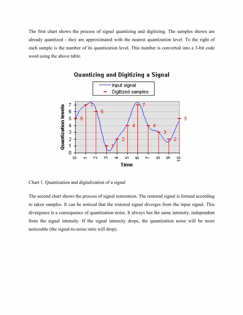
The first chart shows the process of signal quantizing and digitizing. The samples shown are
already quantized - they are approximated with the nearest quantization level. To the right of
each sample is the number of its quantization level. This number is converted into a 3-bit code
word using the above table.
Chart 1. Quantization and digitalization of a signal
The second chart shows the process of signal restoration. The restored signal is formed according
to taken samples. It can be noticed that the restored signal diverges from the input signal. This
divergence is a consequence of quantization noise. It always has the same intensity, independent
from the signal intensity. If the signal intensity drops, the quantization noise will be more
noticeable (the signal-to-noise ratio will drop).
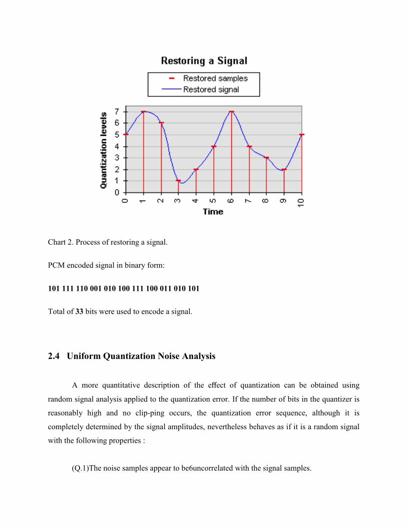
Chart 2. Process of restoring a signal.
PCM encoded signal in binary form:
101 111 110 001 010 100 111 100 011 010 101
Total of 33 bits were used to encode a signal.
2.4 Uniform Quantization Noise Analysis
A more quantitative description of the effect of quantization can be obtained using
random signal analysis applied to the quantization error. If the number of bits in the quantizer is
reasonably high and no clip-ping occurs, the quantization error sequence, although it is
completely determined by the signal amplitudes, nevertheless behaves as if it is a random signal
with the following properties :
(Q.1)The noise samples appear to be6uncorrelated with the signal samples.
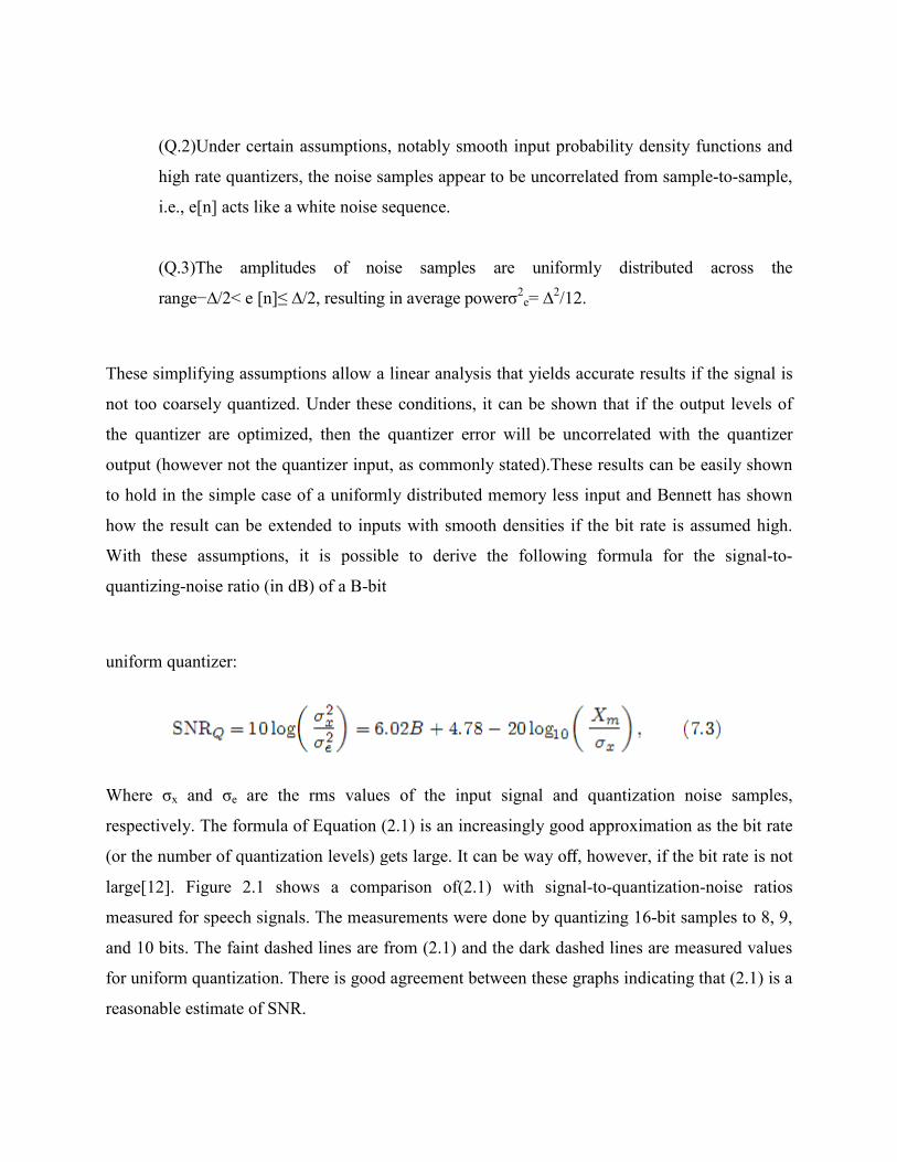
(Q.2)Under certain assumpt
high rate quantizers, the noise samples appear to be uncorrelated from sample
i.e., e[n] acts like a white noise sequence.
(Q.3)The amplitudes of
range−∆/2< e [n]≤ ∆/2, resulting
These simplifying assumptions allow a linear analysis that yields accurate results if the signal is
not too coarsely quantized. Under these conditions, it can be shown that if the output levels of
the quantizer are optimized, then the quantizer error will
output (however not the quantizer input, as commonly stated).These results can be easily shown
to hold in the simple case of a uniformly distributed memory
how the result can be extended t
With these assumptions, it is possible to derive the following formula for the signal
quantizing-noise ratio (in dB) of a
uniform quantizer:
Where σx and σe are the rms values of t
respectively. The formula of Equation (
(or the number of quantization levels) gets large. It can be way o
large[12]. Figure 2.1 shows a comparison of(
measured for speech signals. The measurements were done by quantizing 16
and 10 bits. The faint dashed lines are from (
for uniform quantization. There is good agreement between these graphs indicating that (
reasonable estimate of SNR.
(Q.2)Under certain assumptions, notably smooth input probability density functions and
noise samples appear to be uncorrelated from sample
e[n] acts like a white noise sequence.
(Q.3)The amplitudes of noise samples are uniformly distributed across the
2, resulting in average powerσ2
e= ∆2/12.
These simplifying assumptions allow a linear analysis that yields accurate results if the signal is
not too coarsely quantized. Under these conditions, it can be shown that if the output levels of
optimized, then the quantizer error will be uncorrelated with the quantizer
output (however not the quantizer input, as commonly stated).These results can be easily shown
to hold in the simple case of a uniformly distributed memory less input and Bennett has shown
result can be extended to inputs with smooth densities if the bit rate is assumed high.
With these assumptions, it is possible to derive the following formula for the signal
noise ratio (in dB) of a B-bit
are the rms values of the input signal and quantization noise samples,
respectively. The formula of Equation (2.1) is an increasingly good approximation as the bit rate
(or the number of quantization levels) gets large. It can be way off, however, if the bit rate is not
shows a comparison of(2.1) with signal-to-quantization
measured for speech signals. The measurements were done by quantizing 16-bit samples to 8, 9,
and 10 bits. The faint dashed lines are from (2.1) and the dark dashed lines are measured values
for uniform quantization. There is good agreement between these graphs indicating that (
ability density functions and
noise samples appear to be uncorrelated from sample-to-sample,
tributed across the
These simplifying assumptions allow a linear analysis that yields accurate results if the signal is
not too coarsely quantized. Under these conditions, it can be shown that if the output levels of
be uncorrelated with the quantizer
output (however not the quantizer input, as commonly stated).These results can be easily shown
ess input and Bennett has shown
is assumed high.
With these assumptions, it is possible to derive the following formula for the signal-to-
he input signal and quantization noise samples,
) is an increasingly good approximation as the bit rate
, however, if the bit rate is not
quantization-noise ratios
bit samples to 8, 9,
re measured values
for uniform quantization. There is good agreement between these graphs indicating that (2.1) is a
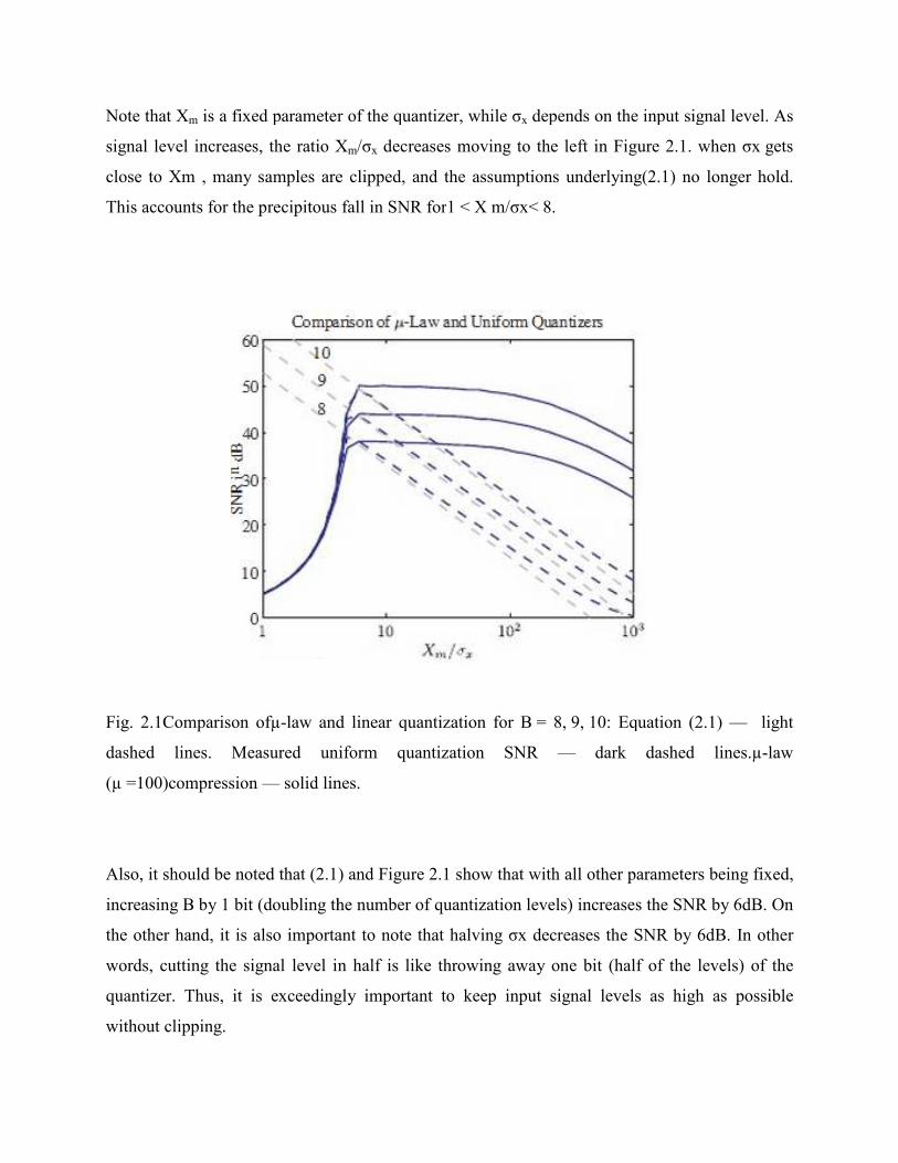
Note that Xm is a fixed parameter of the quantizer, while
signal level increases, the ratio X
close to Xm , many samples are clipped, and the assumptions underlying(
This accounts for the precipitous fall in SNR for
Fig. 2.1Comparison ofµ-law and linear quantization for
dashed lines. Measured uniform quantization SNR
(µ =100)compression — solid lines.
Also, it should be noted that (2.1
increasing B by 1 bit (doubling the number of quantization levels) increases the SNR by 6dB. On
the other hand, it is also important to note that halving
words, cutting the signal level in half is like throwing away one bit (half of the levels) of the
quantizer. Thus, it is exceedingly important to keep input signal levels as high as possible
without clipping.
xed parameter of the quantizer, while σx depends on the input signal level. As
Xm/σx decreases moving to the left in Figure 2.1
, many samples are clipped, and the assumptions underlying(2.1) no longer hold.
This accounts for the precipitous fall in SNR for1 < X m/σx< 8.
law and linear quantization for B = 8, 9, 10: Equation (
dashed lines. Measured uniform quantization SNR — dark dashed lines.
solid lines.
2.1) and Figure 2.1 show that with all other parameters being
by 1 bit (doubling the number of quantization levels) increases the SNR by 6dB. On
the other hand, it is also important to note that halving σx decreases the SNR by 6dB. In other
words, cutting the signal level in half is like throwing away one bit (half of the levels) of the
quantizer. Thus, it is exceedingly important to keep input signal levels as high as possible
depends on the input signal level. As
2.1. when σx gets
) no longer hold.
10: Equation (2.1) — light
dark dashed lines.µ-law
with all other parameters being fixed,
by 1 bit (doubling the number of quantization levels) increases the SNR by 6dB. On
by 6dB. In other
words, cutting the signal level in half is like throwing away one bit (half of the levels) of the
quantizer. Thus, it is exceedingly important to keep input signal levels as high as possible
2.5 Aperture Time
PCM Sampling
- the function of a sampling circuit in a PCM transmitter is to periodically sample the
continually changing analog input voltage and convert those samples to a series of
constant-amplitude pulses that can be more easily be converted to binary PCM code
- For the ADC to accurately convert a voltage to binary code, the voltage must be
relatively constant so that the ADC can complete the conversion before the voltage level
changes. If not, the ADC would be continually attempting to follow the changes and may
never stabilize on any PCM code.
o Two basic techniques used to perform the sampling function:
natural sampling
flat-top sampling
Natural sampling
– is when the tops of the sample pulses retain their natural shape during the sample interval,
making it difficult for an ADC to convert the sample to a PCM code
Flat-top sampling
- is the most common method used for sampling voice signals in PCM systems, which is
accomplished in a sample-and-hold circuit
- the purpose of a sample-and-hold circuit is to periodically sample the continually
changing analog input voltage and convert those samples to a series of constant-
amplitude PAM voltage levels
aperture error – is when the amplitude of the sampled signal changes during the sample pulse
time
aperture or acquisition time – the time that the FET, Q1, of a sample-and-hold circuit is on
aperture distortion – if the input to the ADC is changing while it is performing the conversion
droop – a gradual discharge across the capacitor of a sample-and-hold circuit during conversion
time caused by the capacitor discharging through its own leakage resistance and the input
impedance of the voltage follower Z2
2.6 Summary
Today and in the future, research will be concentrated on developing new PCM signal
compression methods. These compression methods should have higher compression rates,
probably over 100:1 with unnoticeable loss in signal quality. The basic signal quality is
measured by human perception, so various segments of human perception are being studied in
detail. According to these studies compression methods are formed, the signal restored after
compression has only components of the original signal which are above the threshold of
perception. In the 80's compression methods was based on classical information theory. The
basic technique was to find redundancy in data (images, etc.) and according to that to conduct the
compression. Compression of images is segment of data compression which was probably
mostly exploited. So image-compression based on the techniques described above can be called
first generation image coding techniques. The second generation image coding techniques takes
in consideration various aspects of human visual system in order to achieve greater compression
rates without significant loss of image quality. That means that those coding techniques are
lossy, but an important characteristic of this technique is in that it identifies and separate visually
relevant and irrelevant parts of an image and then uses appropriate coding techniques for these
parts.
2.7 Keywords
• PCM
• PAM
• Natural sampling
• Flat-top sampling
• Aperture or acquisition time
2.8 Exercise
1. Explain PCM Reception And Noise.
2. Explain Uniform Quantization Noise Analysis.
3. Define Aperture Time.
Unit 3
Pulse Code Modulation-2
Structure
3.1 Introduction
3.2 Objectives
3.3 The S N Ratio And Channel Capacity Of PCM
3.4 Comparison Of PCM With Other Systems
3.5 Pulse rate
3.6 Advantages and applications of Pulse Code Modulation
3.7 Disadvantages of Pulse Code Modulation
3.8 Summary
3.10 Exercise
3.9 Keywords
3.1 Introduction
PCM uses binary numbers to represent each position of the servo. Binary numbers are
integers or whole numbers. There is a finite or limited amount of numbers available to represent
the servo position based on how many bits the system has available. The amount of numbers
available will be 2 to the power of #bits. If it is a 10-bit system there will be 2^10=1024 numbers
available.
Let’s just say we have a 10-bit system with 1024 servo positions. This is digital because there are
only 1024 different positions that the servo can be positioned, with nothing in between those
numbers. In contrast, a PPM system has an infinite amount of positions available which makes it
is analogue.
3.2 Objectives
At the end of this chapter you will be able to:
• Give the S N Ratio And Channel Capacity Of PCM
• Give the Comparison Of PCM With Other Systems
• Define Pulse rate
• List the Advantages and applications of Pulse Code Modulation
• List Disadvantages of Pulse Code Modulation
3.3 The S N Ratio and Channel Capacity of PCM
How fast can we transmit information over a communication channel?
Suppose a source sends r messages per second, and the entropy of a message is H bits per
message. The information rate is R D r H bits/second.
One can intuitively reason that, for a given communication system, as the information rate
increases the number of errors per second will also increase. Surprisingly, however, this is not
the case.
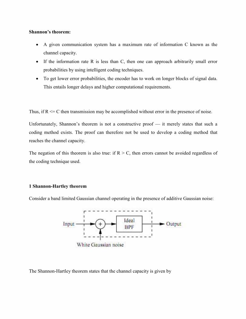
Shannon’s theorem:
• A given communication system has a maximum rate of information C known as the
channel capacity.
• If the information rate R is less than C, then one can approach arbitrarily smal
probabilities by using intelligent coding techniques.
• To get lower error probabilities, the encoder has to work on longer blocks of signal data.
This entails longer delays and higher computational requirements.
Thus, if R <= C then transmission ma
Unfortunately, Shannon’s theorem is not a constructive proof
coding method exists. The proof can therefore not be used to develop a coding method that
reaches the channel capacity.
The negation of this theorem is also true: if R > C, then errors cannot be avoided regardless of
the coding technique used.
1 Shannon-Hartley theorem
Consider a band limited Gaussian channel operating in the presence of additive Gaussian
The Shannon-Hartley theorem states that the channel capacity is given by
A given communication system has a maximum rate of information C known as the
If the information rate R is less than C, then one can approach arbitrarily smal
probabilities by using intelligent coding techniques.
To get lower error probabilities, the encoder has to work on longer blocks of signal data.
This entails longer delays and higher computational requirements.
Thus, if R <= C then transmission may be accomplished without error in the presence of noise.
Unfortunately, Shannon’s theorem is not a constructive proof — it merely states that such a
coding method exists. The proof can therefore not be used to develop a coding method that
The negation of this theorem is also true: if R > C, then errors cannot be avoided regardless of
Consider a band limited Gaussian channel operating in the presence of additive Gaussian
Hartley theorem states that the channel capacity is given by
A given communication system has a maximum rate of information C known as the
If the information rate R is less than C, then one can approach arbitrarily small error
To get lower error probabilities, the encoder has to work on longer blocks of signal data.
y be accomplished without error in the presence of noise.
it merely states that such a
coding method exists. The proof can therefore not be used to develop a coding method that
The negation of this theorem is also true: if R > C, then errors cannot be avoided regardless of
Consider a band limited Gaussian channel operating in the presence of additive Gaussian noise:
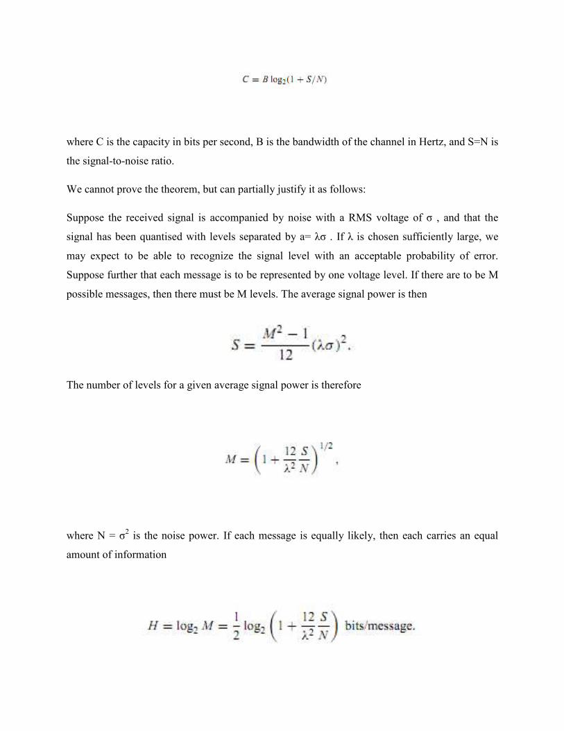
where C is the capacity in bits per second, B is the bandwidth of the channel in Hertz, and S=N is
the signal-to-noise ratio.
We cannot prove the theorem, but can partial
Suppose the received signal is accompanied by noise with a RMS voltage of σ , and that the
signal has been quantised with levels separated by
may expect to be able to recognize
Suppose further that each message is to be represented by one voltage level. If there
possible messages, then there must be M levels. The average
The number of levels for a given average signal power is therefore
where N = σ2 is the noise power. If each message is equally likely, then each carries an equal
amount of information
where C is the capacity in bits per second, B is the bandwidth of the channel in Hertz, and S=N is
We cannot prove the theorem, but can partially justify it as follows:
uppose the received signal is accompanied by noise with a RMS voltage of σ , and that the
signal has been quantised with levels separated by a= λσ . If λ is chosen sufficiently
recognize the signal level with an acceptable probability of error.
further that each message is to be represented by one voltage level. If there
possible messages, then there must be M levels. The average signal power is then
vels for a given average signal power is therefore
is the noise power. If each message is equally likely, then each carries an equal
where C is the capacity in bits per second, B is the bandwidth of the channel in Hertz, and S=N is
uppose the received signal is accompanied by noise with a RMS voltage of σ , and that the
sufficiently large, we
probability of error.
further that each message is to be represented by one voltage level. If there are to be M
signal power is then
is the noise power. If each message is equally likely, then each carries an equal
To find the information rate, we need to estimate how many messages can be carri
time by a signal on the channel. Since the discussion is heuristic, we note that the response of an
ideal LPF of bandwidth B to a unit step has a 10
therefore that with T = 0.5 / B ≈
rate is then
The rate at which information is being transferred across the channel is Therefore
This is equivalent to the Shannon
estimated the rate at which information can be transmitted with reasonably small error
Shannon-Hartley theorem indicates that with
transmission at channel capacity can occur with arbitrarily small error.
The expression of the channel capacity of the Gaussian channel makes intuitive sense:
• As the bandwidth of the channel increases, it is possible to make faster changes in the
information signal, thereby increasing the information rate.
• As S/N increases, one can increase the information rate while still preventing errors due
to noise.
• For no noise, S/N= ∞
bandwidth
Thus we may trade off bandwidth for SNR. For example, if S/N= 7 and B= 4kHz, then the
channel capacity is C = 12* 103
3kHz, the channel capacity remains the same.
nd the information rate, we need to estimate how many messages can be carri
time by a signal on the channel. Since the discussion is heuristic, we note that the response of an
ideal LPF of bandwidth B to a unit step has a 10–90 percent rise time of τ = 0.44/B. We estimate
≈ τ we should be able to reliably estimate the level. The message
The rate at which information is being transferred across the channel is Therefore
This is equivalent to the Shannon-Hartley theorem with λ= 3:5. Note that this discussion has
the rate at which information can be transmitted with reasonably small error
Hartley theorem indicates that with sufficiently advanced coding techniques
transmission at channel capacity can occur with arbitrarily small error.
of the channel capacity of the Gaussian channel makes intuitive sense:
As the bandwidth of the channel increases, it is possible to make faster changes in the
information signal, thereby increasing the information rate.
As S/N increases, one can increase the information rate while still preventing errors due
and an infinite information rate is possible irrespective of
Thus we may trade off bandwidth for SNR. For example, if S/N= 7 and B= 4kHz, then the
bits/s. If the SNR increases to S=N D 15 and B is decreased to
3kHz, the channel capacity remains the same.
nd the information rate, we need to estimate how many messages can be carried per unit
time by a signal on the channel. Since the discussion is heuristic, we note that the response of an
90 percent rise time of τ = 0.44/B. We estimate
be able to reliably estimate the level. The message
The rate at which information is being transferred across the channel is Therefore
Hartley theorem with λ= 3:5. Note that this discussion has
the rate at which information can be transmitted with reasonably small error — the
advanced coding techniques
of the channel capacity of the Gaussian channel makes intuitive sense:
As the bandwidth of the channel increases, it is possible to make faster changes in the
As S/N increases, one can increase the information rate while still preventing errors due
nite information rate is possible irrespective of
Thus we may trade off bandwidth for SNR. For example, if S/N= 7 and B= 4kHz, then the
bits/s. If the SNR increases to S=N D 15 and B is decreased to
However, as B =>∞, the channel
bandwidth, the noise power also increases. If the noise power spectral density is
total noise power is N = ηB, so the Shannon
Noting that
and identifying x as x = S/ηB, the channel capacity as B increases without bound becomes
This gives the maximum information transmission rate possible for a system of given power but
no bandwidth limitations.
The power spectral density can be speci
There are literally dozens of coding techniques
and it is an active research subject. Obviously all obey the Shannon
Some general characteristics of the
sending binary digits at a transmission rate equal to the channel capacity: R
, the channel capacity does not become infinite since, with an increase in
bandwidth, the noise power also increases. If the noise power spectral density is
B, so the Shannon-Hartley law becomes
g x as x = S/ηB, the channel capacity as B increases without bound becomes
This gives the maximum information transmission rate possible for a system of given power but
The power spectral density can be specified in terms of equivalent noise temperature by η=kT
There are literally dozens of coding techniques — entire textbooks are devoted to the subject,
and it is an active research subject. Obviously all obey the Shannon-Hartley theorem.
Some general characteristics of the Gaussian channel can be demonstrated. Suppose we are
sending binary digits at a transmission rate equal to the channel capacity: R = C. If the average
nite since, with an increase in
bandwidth, the noise power also increases. If the noise power spectral density is η /2, then the
g x as x = S/ηB, the channel capacity as B increases without bound becomes
This gives the maximum information transmission rate possible for a system of given power but
uivalent noise temperature by η=kTeq .
entire textbooks are devoted to the subject,
Hartley theorem.
Gaussian channel can be demonstrated. Suppose we are
C. If the average
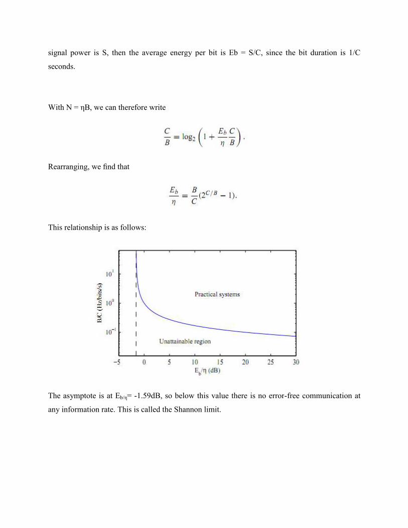
signal power is S, then the average energy per bit is Eb
seconds.
With N = ηB, we can therefore write
Rearranging, we find that
This relationship is as follows:
The asymptote is at Eb/η= -1.59dB, so below this value there is no error
any information rate. This is called the Shannon limit.
average energy per bit is Eb = S/C, since the bit duration is 1
With N = ηB, we can therefore write
1.59dB, so below this value there is no error-free communication at
any information rate. This is called the Shannon limit.
C, since the bit duration is 1/C
free communication at
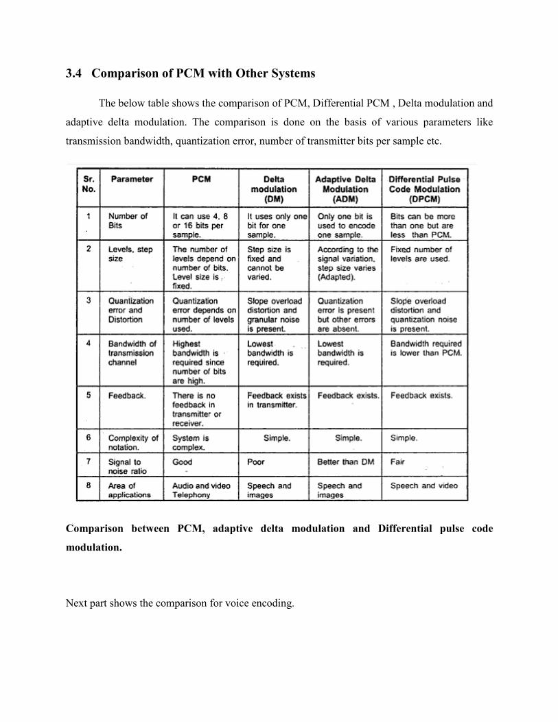
3.4 Comparison of PCM w
The below table shows the comparison
adaptive delta modulation. The comparison is done on the basis of various parameters like
transmission bandwidth, quantization error, number of transmitter bits per sample etc.
Comparison between PCM, adaptive delta modulation and D
modulation.
Next part shows the comparison for voice encoding.
with Other Systems
The below table shows the comparison of PCM, Differential PCM , Delta modulation and
adaptive delta modulation. The comparison is done on the basis of various parameters like
transmission bandwidth, quantization error, number of transmitter bits per sample etc.
Comparison between PCM, adaptive delta modulation and Differential pulse code
Next part shows the comparison for voice encoding.
Delta modulation and
adaptive delta modulation. The comparison is done on the basis of various parameters like
transmission bandwidth, quantization error, number of transmitter bits per sample etc.
ifferential pulse code
3.5 Pulse rate
Sampling is obviously a key feature of PCM system. What sampling rate or pulse rate
must be used for a given signal?
must be at least twice the highest frequency of the input signal.
band limited to 4 kilohertz, a minimum sampling rate of 8 kilo samples per second would be
required. This is typical of a voice channel in a telecommunication channel. If the same signal
sample is quantized to 8 bits (28
(8 bits per sample times 8 kilo samples per second).
3.5.1 Bits per Second, Symbols per Second and Bauds
Information rate is normally expressed in “bits per second” where a bit represents a bin
choice, i.e., the information is either a “one” or a “zero
over a communication channel, one, or more, bits are encoded into “symbols” which are
transmitted and the transmission rate is expressed in terms of “sy
“baud” is used interchangeably with symbol rate. It is incorrect it refer to “baud rate” since baud
is defined as a measure of rate. Note that symbol rate is only equal to bit rate when only one bit
is represented by a symbol. It is not uncommon for a transmission symbol to represent several
bits. For example, a 4800 bit per second data modem typically transmits at 1200 baud, or 1200
symbols per second, each symbol representing 4 bits of information.
Sampling is obviously a key feature of PCM system. What sampling rate or pulse rate
signal? The sampling theorem answers that question: the sampling rate
must be at least twice the highest frequency of the input signal. If, in our example, the signal is
band limited to 4 kilohertz, a minimum sampling rate of 8 kilo samples per second would be
required. This is typical of a voice channel in a telecommunication channel. If the same signal
8 = 128 levels), the PCM bit rate would be 64 kilobits per second
(8 bits per sample times 8 kilo samples per second).
Bits per Second, Symbols per Second and Bauds
Information rate is normally expressed in “bits per second” where a bit represents a bin
, i.e., the information is either a “one” or a “zero”. When binary information is transmitted
over a communication channel, one, or more, bits are encoded into “symbols” which are
transmitted and the transmission rate is expressed in terms of “symbols per second”. The unit
“baud” is used interchangeably with symbol rate. It is incorrect it refer to “baud rate” since baud
is defined as a measure of rate. Note that symbol rate is only equal to bit rate when only one bit
t is not uncommon for a transmission symbol to represent several
bits. For example, a 4800 bit per second data modem typically transmits at 1200 baud, or 1200
symbols per second, each symbol representing 4 bits of information.
Sampling is obviously a key feature of PCM system. What sampling rate or pulse rate
t question: the sampling rate
in our example, the signal is
band limited to 4 kilohertz, a minimum sampling rate of 8 kilo samples per second would be
required. This is typical of a voice channel in a telecommunication channel. If the same signal
8 levels), the PCM bit rate would be 64 kilobits per second
Information rate is normally expressed in “bits per second” where a bit represents a binary
information is transmitted
over a communication channel, one, or more, bits are encoded into “symbols” which are
mbols per second”. The unit
“baud” is used interchangeably with symbol rate. It is incorrect it refer to “baud rate” since baud
is defined as a measure of rate. Note that symbol rate is only equal to bit rate when only one bit
t is not uncommon for a transmission symbol to represent several
bits. For example, a 4800 bit per second data modem typically transmits at 1200 baud, or 1200
3.6 Advantages and applications of Pulse Code Modulation
The principal advantage of Pulse Code Modulation (PCM) is the noise immunity. But it
is not used exclusively. Other pulse modulation systems are still used in spite of highly superior
performance of PCM. The reasons are that firstly those systems came earlier secondly PCM
needs very complex encoding and quantizing circuitry and thirdly PCM requires larger
bandwidth as compared to analog systems.
In spite of these three implementations PCM is fast gaining popularity and is being used
increasingly. The reasons are very simple. PCM no doubt requires much more complex
modulating procedures than analog systems. But multiplexing equipment is much cheaper.
Further distance between repeaters is large because PCM tolerates much worse signal to noise
ratios. Finally advent of very large scale integration (VLSI) has reduced the cost of complex
circuits needed in PCM. Regarding the increased bandwidth requirements by PCM the problems
is no longer a serious one because of the advent of large band width fiber optic systems. PCM
also finds use in space communications. Way back in 1965 PCM was used by mariners to
transmit back pictures of Mars. Of course each picture took several minutes for transmission.
PCM was obviously the first digital system. However, today several others have come up and are
being used occasionally. Few of them are differential PCM and delta modulation. Differential
modulation is a PCM with the modification that each word in this system indicates the difference
in amplitude, positive or negative, between this sample and the previous one. Thus this system
indicates the relative rather than the absolute value of each sample. In this, therefore, the speech
is redundant, since amplitude is related to the previous one and large variations from one sample
to the next are unlikely. As a result fewer bits are needed to indicate the size of the magnitude
change relative to the case of absolute magnitude. Smaller bandwidth is therefore needed for
transmission. Differential PCM is not popularly used because increased complexity of encoding
and decoding processes outweighs advantages and gained through its use.
Delta modulation is a digital modulation system which in its simplest form may be
equated with the basic form of differential PCM. In a simple delta modulation system just one bit
is sent per sample to indicate whether the signal is larger or smaller than the previous sample.
This system has the merits of having extremely simple coding and decoding procedures. Further
the quantizing process is also very simple. But it has the drawback that it can not easily handle
rapid changes in magnitude and as a result quantizing noise tends to be quite high. Even on using
compounding and modified and complex versions of delta modulation, the transmission race
must be close to hundred kilo bits per second to give the same performance for a telephone
channel as PCM provides with only sixty four kilo bits.
3.7 Disadvantages of Pulse Code Modulation
The advantage of a PCM radio system is that it gives the pilot much finer and more precise
control over the airplane. However, there is a huge drawback. A PCM receiver must translate the
signal from Pulse Code Modulation language to Pulse Position Modulation language before
sending the information to the servos.
If one small byte of information is corrupt, even if it is only for one servo, the translator inside
the receiver gets all confused! The "translator" part of the receiver looks at ALL of the servos
and says “I don’t understand a word the transmitter is saying, so all of you hold your position
until I get the next message!” If only a couple of messages or sequences of information is
corrupt, the pilot will never notice because the servos will stay put at the position of the last
known good signal for a very short period of time (20ms for each bad or corrupt message).
If the signal is corrupt for an extended period of time a PCM receiver will enter “safe mode”.
Safe mode moves all of the servos to a predetermined position. At this point Sir Isaac Newton is
piloting your airplane! Since he’s been dead for a while this is not a good thing!
3.8 Summary
The advantage of a digital signal is that it can be reproduced perfectly. The information is always
decoded as a 0 or 1. There are no gray areas in between to create noise. This means that the
information arriving at the receiver is exactly the same as the information leaving the transmitter.
In contrast, a PPM analogue signal could be distorted by slight interference before it arrives at
the receiver. The Pulse Position Modulation receiver will pass all of the information it gets to the
servos, including interference.
3.9 Keywords
• PCM
• DM
• ADM
• DPCM
3.10 Exercise
1. Give the S N Ratio and Channel capacity of PCM.
2. Give the comparison of PCM with other Systems.
3. Define Pulse rate.
4. List the Advantages and applications of Pulse Code Modulation.
5. List Disadvantages of Pulse Code Modulation.
Unit 4
Pulse Code Modulation-3
Structure
4.1 Introduction
4.2 Objectives
4.3 PCM Codescs
4.4 24-Channel PCM
4.5 The PCM Channel Bank
4.6 Multiplex Hierarchy
4.7 Measurements of Quantization Noise
4.8 Differential PCM
4.9 Summary
4.10 Keywords
4.11 Exercise
4.1 Introduction
Meaning of DPCM – “Differential Pulse Code Modulation”, is a modulation technique
invented by the British Alec Reeves in 1937. It is a digital representation of an analog signal
where the magnitude of the signal is sampled regularly at uniform intervals. Every sample is
quantized to a series of symbols in a digital code, which is usually a binary code. PCM is used in
digital telephone systems. It is also the standard form for digital audio in computers and various
compact disc formats. Several PCM streams may be multiplexed into a larger aggregate data
stream. This technique is called Time-Division Multiplexing, or (TDM). TDM was invented by
the telephone industry, but today the technique is an integral part of many digital audio
workstations such as Pro Tools. In conventional PCM, the analog signal may be processed (e.g.
by amplitude compression) before being digitized. Once the signal is digitized, the PCM signal is
not subjected to further processing (e.g. digital data compression). Some forms of PCM combine
signal processing with coding. Older versions of these systems applied the processing in the
analog domain as part of the A/D process; newer implementations do so in the digital domain.
These simple techniques have been largely rendered obsolete by modern transform-based signal
compression techniques.
4.2 Objectives
At the end of this chapter you will be able to:
• Know PCM Codes.
• Explain 24-Channel PCM.
• Explain the PCM Channel Bank.
• Know Multiplex Hierarchy.
• Define DPCM.
4.3 PCM Codecs
Pulse Code Modulation (PCM) codecs are the simplest form of waveform codecs.
Narrowband speech is typically sampled 8000 times per second, and then each speech sample
must be quantized. If linear quantization is used then about 12 bits per sample are needed, giving
a bit rate of about 96 kbits/s. However this can be easily reduced by using non-linear
quantization. For coding speech it was found that with non-linear quantization 8 bits per sample
was sufficient for speech quality which is almost indistinguishable from the original. This gives a
bit rate of 64 kbits/s, and two such non-linear PCM codecs were standardised in the 1960s. In
America u-law coding is the standard, while in Europe the slightly different A-law compression
is used. Because of their simplicity, excellent quality and low delay both these codecs are still
widely used today. For example the .au audio files that are often used to convey sounds over the
Web are in fact just PCM files. For information on how to listen to au and other sound format
files under various operating systems. Code to implement the G711 A-law and u-law codes has
been released into the public domain by Sun Microsystems Inc, and modified by Borge
Lindberg. To FTP this code. For more information about PCM, and other waveform codecs, a
good place to look is the book "Digital Coding of Waveforms" by N.S Jayant and Peter Noll. It
was published by Prentice Hall in 1984, and although its too expensive really to be worth buying,
you might find a copy in your library.
4.4 24-Channel PCM
Time division multiplexing is used at local exchanges to combine a number of
incoming voice signals onto an outgoing trunk. Each incoming channel is allocated a
specific time slot on the outgoing trunk, and has full access to the transmission line
only during its particular time slot. Because the incoming signals are analogue, they
must first be digitized, because TDM can only handle digital signals. Because PCM
samples the incoming signals 8000 times per second, each sample occupies 1/8000
seconds (125 µseconds). PCM is at the heart of the modern telephone system, and
consequently, nearly all time intervals used in the telephone system are multiples of
125 µseconds.
Because of a failure to agree on an international standard for digital transmission, the
systems used in Europe and North America are different. The North American
standard is based on a 24-channel PCM system, wheras the European system is based
on 4.6.2/4.6.4 channels. This system contains 4.6.2 speech channels, a synchronisation
channel and a signalling channel, and the gross line bit rate of the system is 2.048
Mbps (4.6.4 x 64 Kbps). The system can be adapted for common channel signalling,
providing 4.6.3 data channels and employing a single synchronisation channel. The
following details refer to the European system.
The 4.6.2/4.6.4 channel system uses a frame and multiframe structure, with each frame
consisting of 4.6.4 pulse channel time slots numbered 0-4.6.3. Slot 0 contains
the Frame Alignment Word (FAW) and Frame Service Word (FSW). Slots 1-15 and
17-4.6.3 are used for digitised speech (channels 1-15 and 16-4.6.2 respectively). In
each digitised speech channel, the first bit is used to signify the polarity of the sample,
and the remaining bits represent the amplitude of the sample. The duration of each bit
on a PCM system is 488 nanoseconds (ns). Each time slot is therefore 3.904 µseconds
(8 bits x 488 ns). Each frame therefore occupies 125 milliseconds (4.6.4 x 3.904
mseconds).
In order for signalling information (dial pulses) for all 4.6.2 channels to be transmitted,
the multiframe consists of 16 frames numbered 0-15. In frame 0, slot 16 contains the
Multiframe Alignment Word (MFAW) and Multiframe Service Word (MFSW). In
frames 1-15, slot 16 contains signalling information for two channels. The frame and
multiframe structure are shown below. The duration of each multiframe is 2
milliseconds(125 µseconds x 16).
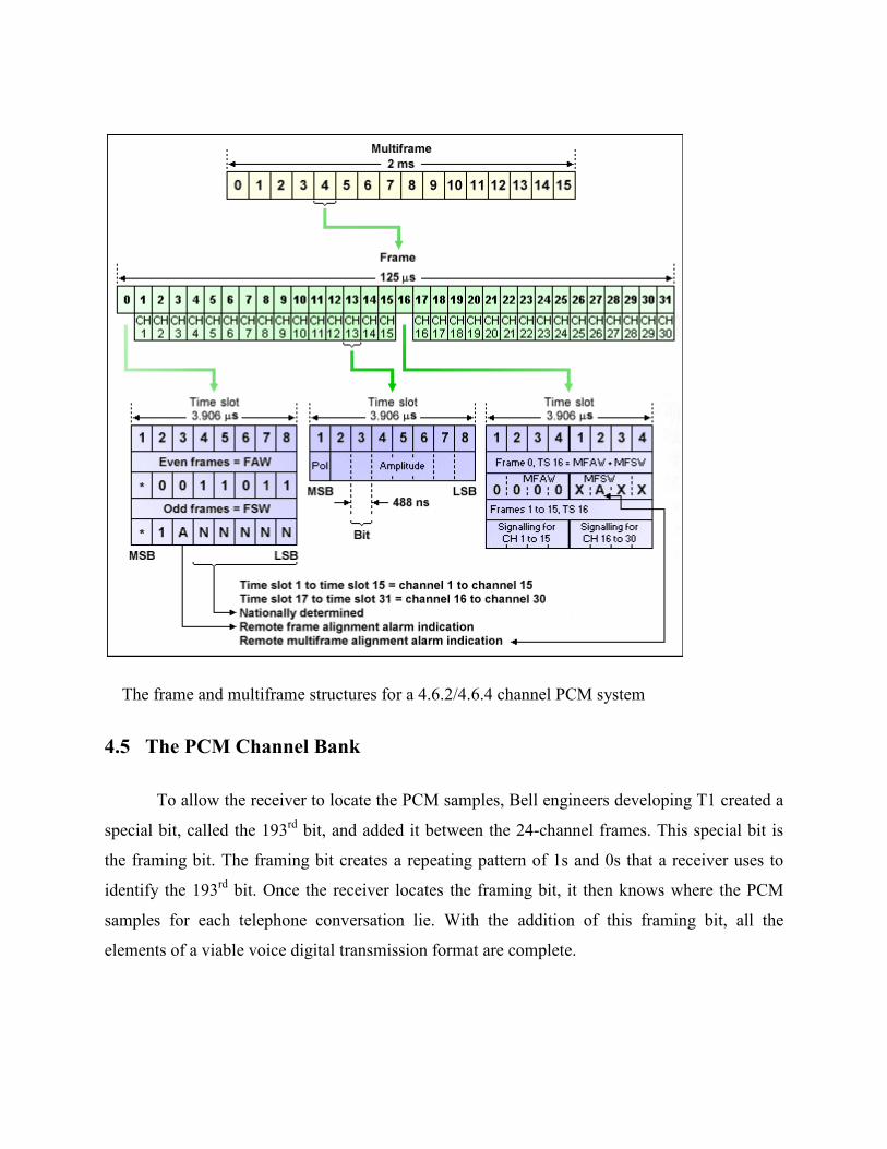
The frame and multiframe structures for a 4.6.2/4.6.4 channel PCM system
4.5 The PCM Channel Bank
To allow the receiver to locate the PCM samples, Bell engineers developing T1 created a
special bit, called the 193rd
bit, and added it between the 24-channel frames. This special bit is
the framing bit. The framing bit creates a repeating pattern of 1s and 0s that a receiver uses to
identify the 193rd
bit. Once the receiver locates the framing bit, it then knows where the PCM
samples for each telephone conversation lie. With the addition of this framing bit, all the
elements of a viable voice digital transmission format are complete.
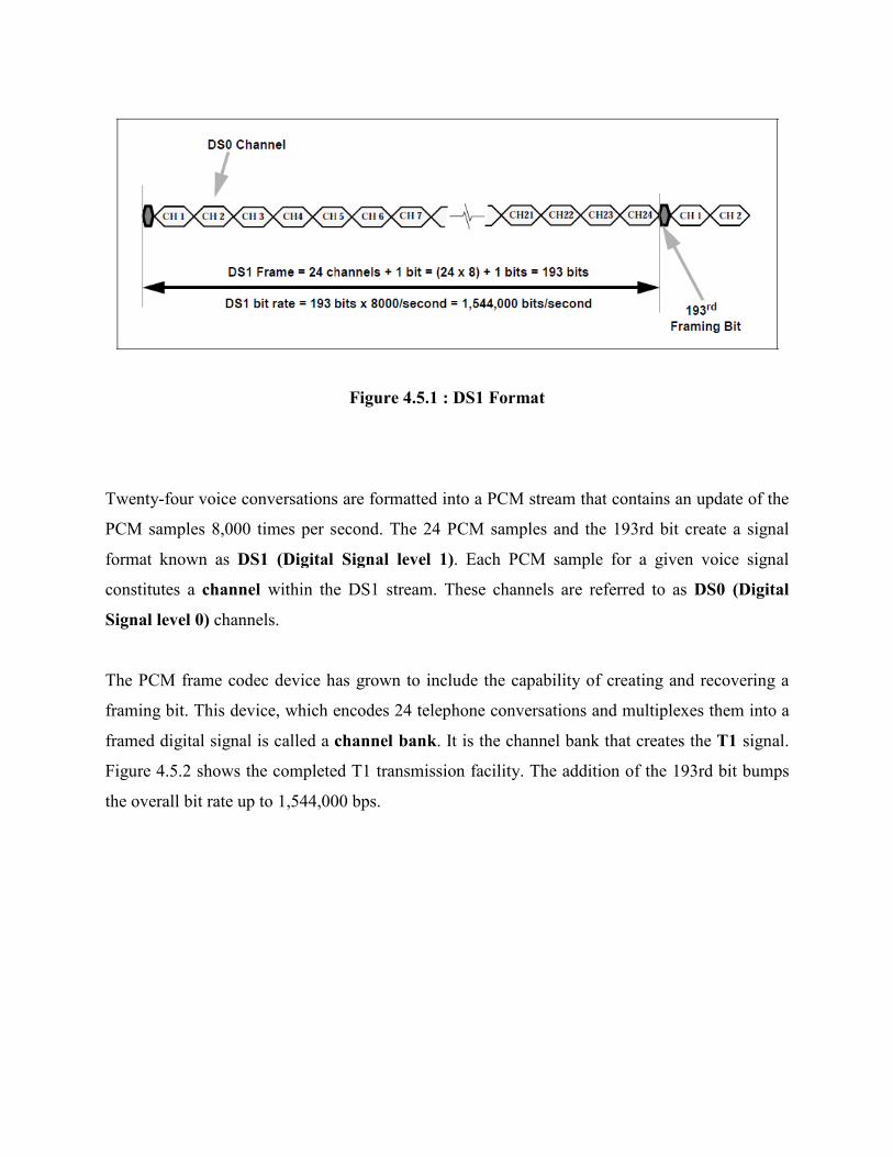
Twenty-four voice conversations are formatted into a PCM stream that contains an update
PCM samples 8,000 times per second. The 24 PCM samples and the 193rd bit create
format known as DS1 (Digital Signal level 1
constitutes a channel within the DS1 stream. These channels are referred to as
Signal level 0) channels.
The PCM frame codec device has grown to include the capability of creating and
framing bit. This device, which encodes 24 telephone conversations and
framed digital signal is called a channel bank
Figure 4.5.2 shows the completed T1 transmission facility.
the overall bit rate up to 1,544,000 bps.
Figure 4.5.1 : DS1 Format
four voice conversations are formatted into a PCM stream that contains an update
PCM samples 8,000 times per second. The 24 PCM samples and the 193rd bit create
DS1 (Digital Signal level 1). Each PCM sample for a given voice
within the DS1 stream. These channels are referred to as
The PCM frame codec device has grown to include the capability of creating and
framing bit. This device, which encodes 24 telephone conversations and multiplexes them into a
channel bank. It is the channel bank that creates the
shows the completed T1 transmission facility. The addition of the 193rd bit bumps
the overall bit rate up to 1,544,000 bps.
four voice conversations are formatted into a PCM stream that contains an update of the
PCM samples 8,000 times per second. The 24 PCM samples and the 193rd bit create a signal
. Each PCM sample for a given voice signal
within the DS1 stream. These channels are referred to as DS0 (Digital
The PCM frame codec device has grown to include the capability of creating and recovering a
multiplexes them into a
bank that creates the T1 signal.
addition of the 193rd bit bumps
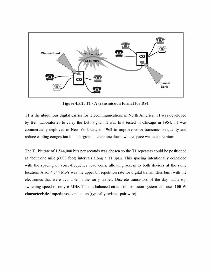
Figure 4.5.2: T1 - A transmission format for DS1
T1 is the ubiquitous digital carrier for telecommunications in North America. T1 was developed
by Bell Laboratories to carry the DS1 signal. It was first tested in Chicago in 1964. T1 was
commercially deployed in New York City in 1962 to improve voice transmission quality and
reduce cabling congestion in underground telephone ducts, where space was at a premium.
The T1 bit rate of 1,544,000 bits per seconds was chosen so the T1 repeaters could be positioned
at about one mile (6000 foot) intervals along a T1 span. This spacing intentionally coincided
with the spacing of voice-frequency load coils, allowing access to both devices at the same
location. Also, 4.544 Mb/s was the upper bit repetition rate for digital transmitters built with the
electronics that were available in the early sixties. Discrete transistors of the day had a top
switching speed of only 6 MHz. T1 is a balanced-circuit transmission system that uses 100 W
characteristic-impedance conductors (typically twisted-pair wire).
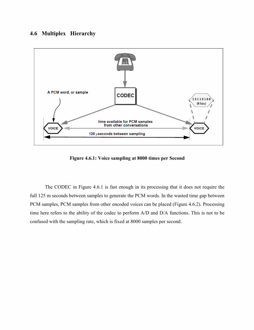
4.6 Multiplex Hierarchy
Figure 4.6.1: Voice sampling at 8000 times per Second
The CODEC in Figure 4.6.1
full 125 m seconds between samples to generate the PCM words. In the wasted time gap
PCM samples, PCM samples from other encoded voices can be placed (Figure
time here refers to the ability of the codec to perform A/D and D/A
confused with the sampling rate, which is fixed at 8000 samples per second.
Multiplex Hierarchy
: Voice sampling at 8000 times per Second
4.6.1 is fast enough in its processing that it does not require the
seconds between samples to generate the PCM words. In the wasted time gap
PCM samples, PCM samples from other encoded voices can be placed (Figure 4.6.2
e refers to the ability of the codec to perform A/D and D/A functions. This is not to be
confused with the sampling rate, which is fixed at 8000 samples per second.
is fast enough in its processing that it does not require the
seconds between samples to generate the PCM words. In the wasted time gap between
4.6.2). Processing
functions. This is not to be
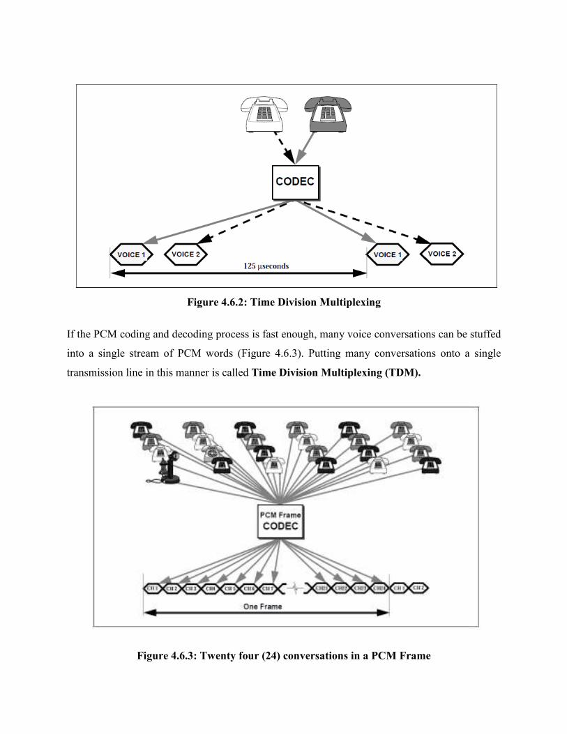
Figure
If the PCM coding and decoding process is fast e
into a single stream of PCM words (Figure
transmission line in this manner is called
Figure 4.6.3: Twenty four (24)
Figure 4.6.2: Time Division Multiplexing
If the PCM coding and decoding process is fast enough, many voice conversations can be
into a single stream of PCM words (Figure 4.6.3). Putting many conversations onto a
transmission line in this manner is called Time Division Multiplexing (TDM).
: Twenty four (24) conversations in a PCM Frame
nough, many voice conversations can be stuffed
). Putting many conversations onto a single
conversations in a PCM Frame
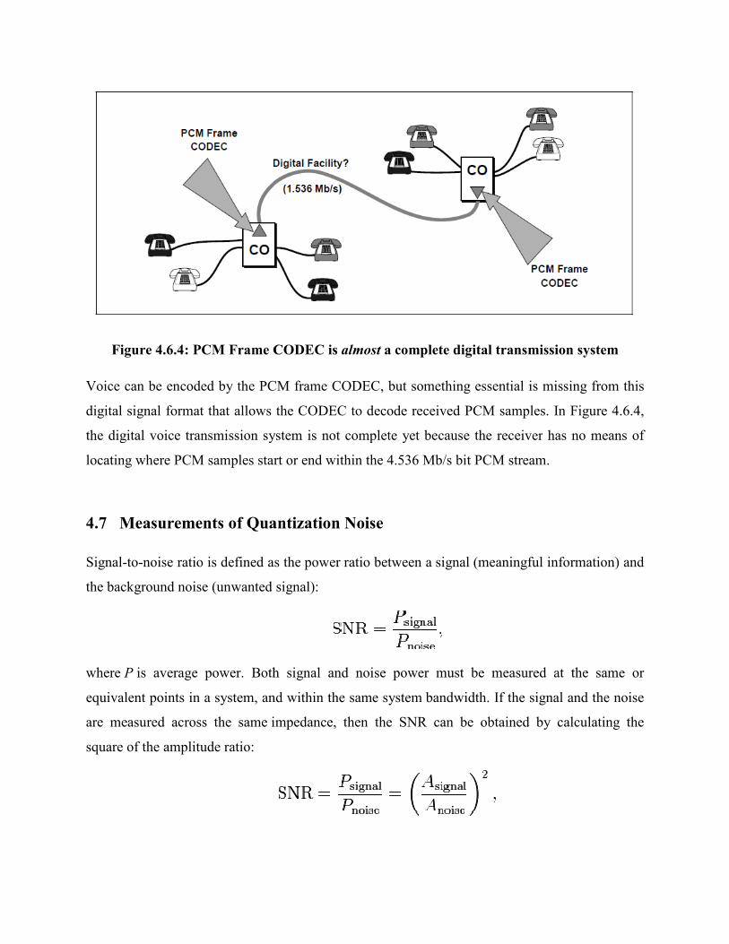
Figure 4.6.4: PCM Frame CODEC is
Voice can be encoded by the PCM frame CODEC, but something essential is missing from
digital signal format that allows the CODEC to decode
the digital voice transmission system is not complete yet because the receiver
locating where PCM samples start or end within the
4.7 Measurements of Quantization Noise
Signal-to-noise ratio is defined as the
the background noise (unwanted signal):
where P is average power. Both signal and noise power must be measured at the same or
equivalent points in a system, and within the same system
are measured across the same impedance
square of the amplitude ratio:
: PCM Frame CODEC is almost a complete digital transmission system
Voice can be encoded by the PCM frame CODEC, but something essential is missing from
digital signal format that allows the CODEC to decode received PCM samples. In
the digital voice transmission system is not complete yet because the receiver
locating where PCM samples start or end within the 4.536 Mb/s bit PCM stream.
f Quantization Noise
noise ratio is defined as the power ratio between a signal (meaningful information) and
(unwanted signal):
is average power. Both signal and noise power must be measured at the same or
oints in a system, and within the same system bandwidth. If the signal and the noise
impedance, then the SNR can be obtained by calculating the
a complete digital transmission system
Voice can be encoded by the PCM frame CODEC, but something essential is missing from this
received PCM samples. In Figure 4.6.4,
has no means of
stream.
(meaningful information) and
is average power. Both signal and noise power must be measured at the same or
. If the signal and the noise
, then the SNR can be obtained by calculating the
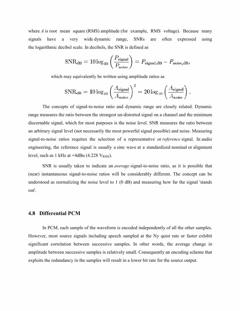
where A is root mean square (RMS)
signals have a very wide
the logarithmic decibel scale. In deci
which may equivalently be written using amplitude ratios as
The concepts of signal-to
range measures the ratio between the strongest un
discernable signal, which for most purposes
an arbitrary signal level (not necessarily the most powerful signal possible) and noise. Measuring
signal-to-noise ratios requires the selection of a representative or
engineering, the reference signal is usually a
level, such as 1 kHz at +4dBu (4.
SNR is usually taken to indicate an
(near) instantaneous signal-to-noise ratios will be considerably different. The concept can be
understood as normalizing the noise level to 1 (0 dB) and measuring how far the signal 's
out'.
4.8 Differential PCM
In PCM, each sample of the waveform is encoded independently of all the other samples.
However, most source signals including speech sampled at the Ny
significant correlation between successive samples. In other words, the average change in
amplitude between successive samples is relatively small. Consequently an encoding scheme that
exploits the redundancy in the samples will res
(RMS) amplitude (for example, RMS voltage). Because many
signals have a very wide dynamic range, SNRs are often expressed using
scale. In decibels, the SNR is defined as
which may equivalently be written using amplitude ratios as
to-noise ratio and dynamic range are closely related. Dynamic
range measures the ratio between the strongest un-distorted signal on a channel and the minimum
discernable signal, which for most purposes is the noise level. SNR measures the ratio between
an arbitrary signal level (not necessarily the most powerful signal possible) and noise. Measuring
noise ratios requires the selection of a representative or reference
, the reference signal is usually a sine wave at a standardized nominal
4.228 VRMS).
en to indicate an average signal-to-noise ratio, as it is possible that
noise ratios will be considerably different. The concept can be
understood as normalizing the noise level to 1 (0 dB) and measuring how far the signal 's
In PCM, each sample of the waveform is encoded independently of all the other samples.
However, most source signals including speech sampled at the Ny quist rate or faster exhibit
significant correlation between successive samples. In other words, the average change in
amplitude between successive samples is relatively small. Consequently an encoding scheme that
exploits the redundancy in the samples will result in a lower bit rate for the source output.
(for example, RMS voltage). Because many
, SNRs are often expressed using
noise ratio and dynamic range are closely related. Dynamic
and the minimum
is the noise level. SNR measures the ratio between
an arbitrary signal level (not necessarily the most powerful signal possible) and noise. Measuring
reference signal. In audio
nominal or alignment
noise ratio, as it is possible that
noise ratios will be considerably different. The concept can be
understood as normalizing the noise level to 1 (0 dB) and measuring how far the signal 'stands
In PCM, each sample of the waveform is encoded independently of all the other samples.
rate or faster exhibit
significant correlation between successive samples. In other words, the average change in
amplitude between successive samples is relatively small. Consequently an encoding scheme that
ult in a lower bit rate for the source output.
A relatively simple solution is to encode the differences between successive samples rather than
the samples themselves. The resulting technique is called differential pulse code modulation
(DPCM). Since differences between samples are expected to be smaller than the actual sampled
amplitudes, fewer bits are required to represent the differences. In this case we quantize and
transmit the differenced signal sequence
e(n)= s(n)- s(n - 1),
where s(n) is the sampled sequence of s(t).
A natural refinement of this general approach is to predict the current sample based on
the previous M samples utilizing linear prediction (LP), where LP parameters are dynamically
estimated. Block diagram of a DPCM encoder and decoder is shown below. Part (a) shows
DPCM encoder and part (b) shows DPCM decoder at the receiver.
The "dpcm_demo" shows the use of DPCM to approximate a input sine wave signal and a
speech signal that were sampled at 2 KHz and 44 KHz, respectively. The source code file of the
MATLAB code and the output can be viewed using MATLAB.
To view these you need to download the zipped MATLAB files and sound file into a directory,
unzip them (example: "unzip fname.zip" on unix), then run demo file on MATLAB. To run the
demo file, type "dpcm_demo" at the MATLAB prompt. (Remember the change directory into the
same directory that the files were placed in.)
4.9 Summary
Signal-to-noise ratio (often abbreviated SNR or S/N) is a measure used in science and
engineering to quantify how much a signal has been corrupted by noise. It is defined as the ratio
of signal power to the noise power corrupting the signal. A ratio higher than 1:1 indicates more
signal than noise. While SNR is commonly quoted for electrical signals, it can be applied to any
form of signal. Differential (or Delta) pulse-code modulation encodes the PCM values as
differences between the current and the previous value. For audio this type of encoding reduces
the number of bits required per sample by about 25% compared to PCM. Adaptive DPCM is a
variant of DPCM that varies the size of the quantization step, to allow further reduction of the
required bandwidth for a given signal-to-noise ratio.
4.10 Keywords
• DPCM
• TDM
• PCM
• FSW
• MFSW
• DS0
• DS1
4.11 Exercise
1. Explain PCM Codecs.
2. Explain 24-Channel PCM.
3. Explain the PCM Channel Bank.
4. Explain Multiplex Hierarchy.
5. Define DPCM.
Unit 1
Introduction to Digital Data Transmission
Structure
1.1 Introduction
1.2 Objectives
1.3 Components of a digital communication system
1.4 Summary
1.5 Keywords
1.6 Exercise
1.1 Introduction
Data transmission, digital transmission, or digital communications is the physical
transfer of data (a digital bit stream) over a point-to-point or point-to-multipoint
communication channel. In this chapter we will go through the introduction part of digital data
transmission.
This chapter is concerned with the transmission of information by electrical means using
digital communication techniques. Information may be transmitted from one point to another
using either digital or analog communication systems. In a digital communication system, the
information is processed so that it can be represented by a sequence of discrete messages as
shown in Figure 1–1. The digital source in Figure 1–1 may be the result of sampling and
quantizing an analog source such as speech, or it may represent a naturally digital source such as
an electronic mail file. In either case, each message is one of a finite set containing q messages.
If q = 2, the source is referred to as a binary source, and the two possible digit values are called
bits, a contraction for binary digits. Note also that source outputs, whether discrete or analog, are
inherently random. If they were not, there would be no need for a communication system.
For example, expanding on the case where the digital information results from an analog
source, consider a sensor whose output voltage at any given time instant may assume a
continuum of values. This waveform may be processed by sampling at appropriately spaced time
instants, quantizing these samples, and converting each quantized sample to a binary number
(i.e., an analog-to-digital converter). Each sample value is therefore represented by a sequence of
1s and 0s, and the communication system associates the message 1 with a transmitted signal s1
(t) and the message 0 with a transmitted signal s0 (t). During each signaling interval either the
message 0 or 1 is transmitted with no other possibilities. In practice, the transmitted signals s0 (t)
and s1 (t) may be conveyed by the following means (other representations are possible):
1. By two different amplitudes of a sinusoidal signal, say, A0 and A1
2. By two different phases of a sinusoidal signal, say, ∏/2 and − ∏/2 radians
3. By two different frequencies of a sinusoidal signal, say, f0 and f1 hertz
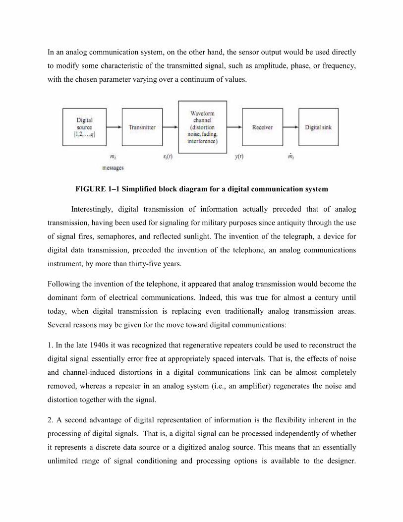
In an analog communication system, on the other hand, the sensor output would be used directly
to modify some characteristic of the transmitted signal, such as amplitude, phase, or fr
with the chosen parameter varying over a continuum of values.
FIGURE 1–1 Simplified block diagram for a digital communication system
Interestingly, digital transmission of information actually preceded that of analog
transmission, having been used for signaling for military purposes since antiquity through the use
of signal fires, semaphores, and reflected sunlight. The invention of the telegraph, a device for
digital data transmission, preceded the invention of the telephone, an analog communica
instrument, by more than thirty-five years.
Following the invention of the telephone, it appeared that analog transmission would become the
dominant form of electrical communications. Indeed, this was true for almost a century until
today, when digital transmission is replacing even traditionally analog transmission areas.
Several reasons may be given for the move toward digital communications:
1. In the late 1940s it was recognized that regenerative repeaters could be used to reconstruct the
digital signal essentially error free at appropriately spaced intervals. That is, the effects of noise
and channel-induced distortions in a digital communications link can be almost completely
removed, whereas a repeater in an analog system (i.e., an amplifier) re
distortion together with the signal.
2. A second advantage of digital representation of information is the flexibility inherent in the
processing of digital signals. That is, a digital signal can be processed independently of wheth
it represents a discrete data source or a digitized analog source. This means that an essentially
unlimited range of signal conditioning and processing options is available to the designer.
In an analog communication system, on the other hand, the sensor output would be used directly
to modify some characteristic of the transmitted signal, such as amplitude, phase, or fr
with the chosen parameter varying over a continuum of values.
1 Simplified block diagram for a digital communication system
Interestingly, digital transmission of information actually preceded that of analog
ed for signaling for military purposes since antiquity through the use
of signal fires, semaphores, and reflected sunlight. The invention of the telegraph, a device for
digital data transmission, preceded the invention of the telephone, an analog communica
five years.
Following the invention of the telephone, it appeared that analog transmission would become the
dominant form of electrical communications. Indeed, this was true for almost a century until
al transmission is replacing even traditionally analog transmission areas.
Several reasons may be given for the move toward digital communications:
1. In the late 1940s it was recognized that regenerative repeaters could be used to reconstruct the
signal essentially error free at appropriately spaced intervals. That is, the effects of noise
induced distortions in a digital communications link can be almost completely
removed, whereas a repeater in an analog system (i.e., an amplifier) regenerates the noise and
distortion together with the signal.
2. A second advantage of digital representation of information is the flexibility inherent in the
processing of digital signals. That is, a digital signal can be processed independently of wheth
it represents a discrete data source or a digitized analog source. This means that an essentially
unlimited range of signal conditioning and processing options is available to the designer.
In an analog communication system, on the other hand, the sensor output would be used directly
to modify some characteristic of the transmitted signal, such as amplitude, phase, or frequency,
1 Simplified block diagram for a digital communication system
Interestingly, digital transmission of information actually preceded that of analog
ed for signaling for military purposes since antiquity through the use
of signal fires, semaphores, and reflected sunlight. The invention of the telegraph, a device for
digital data transmission, preceded the invention of the telephone, an analog communications
Following the invention of the telephone, it appeared that analog transmission would become the
dominant form of electrical communications. Indeed, this was true for almost a century until
al transmission is replacing even traditionally analog transmission areas.
1. In the late 1940s it was recognized that regenerative repeaters could be used to reconstruct the
signal essentially error free at appropriately spaced intervals. That is, the effects of noise
induced distortions in a digital communications link can be almost completely
generates the noise and
2. A second advantage of digital representation of information is the flexibility inherent in the
processing of digital signals. That is, a digital signal can be processed independently of whether
it represents a discrete data source or a digitized analog source. This means that an essentially
unlimited range of signal conditioning and processing options is available to the designer.
Depending on the origination and intended destination of the information being conveyed, these
might include source coding, compression, encryption, pulse shaping for spectral control,
forward error correction (FEC) coding, special modulation to spread the signal spectrum, and
equalization to compensate for channel distortion. These terms and others will be defined and
discussed throughout the book.
3. The third major reason for the increasing popularity of digital data transmission is that it can
be used to exploit the cost effectiveness of digital integrated circuits. Special-purpose digital
signal-processing functions have been realized as large-scale integrated circuits for several years,
and more and more modem functions are being implemented in ever smaller packages (e.g., the
modem card in a laptop computer). The development of the microcomputer and of special
purpose programmable digital signal processors mean that data transmission systems can now be
implemented as software. This is advantageous in that a particular design is not “frozen” as
hardware but can be altered or replaced with the advent of improved designs or changed
requirements.
4. A fourth reason that digital transmission of information is the format of choice in a majority of
applications nowadays is that information represented digitally can be treated the same
regardless of its origin, as already pointed out, but more importantly easily intermixed in the
process of transmission. An example is the Internet, which initially was used to convey packets
or files of information or relatively short text messages. As its popularity exploded in the early
1990s and as transmission speeds dramatically increased, it was discovered that it could be used
to convey traditionally analog forms of information, such as audio and video, along with the
more traditional forms of packetized information.
In the remainder of this chapter, some of the systems aspects of digital communications are
discussed. The simplified block diagram of a digital communications system shown in Figure 1–
1 indicates that any communications system consists of a transmitter, a channel or transmission
medium, and a receiver.
To illustrate the effect of the channel on the transmitted signal, we return to the binary source
case considered earlier. The two possible messages can be represented by the set 0, 1 where
the 0s and ls are called bits (for binary digit) as mentioned previously. If a 0 or a 1 is emitted
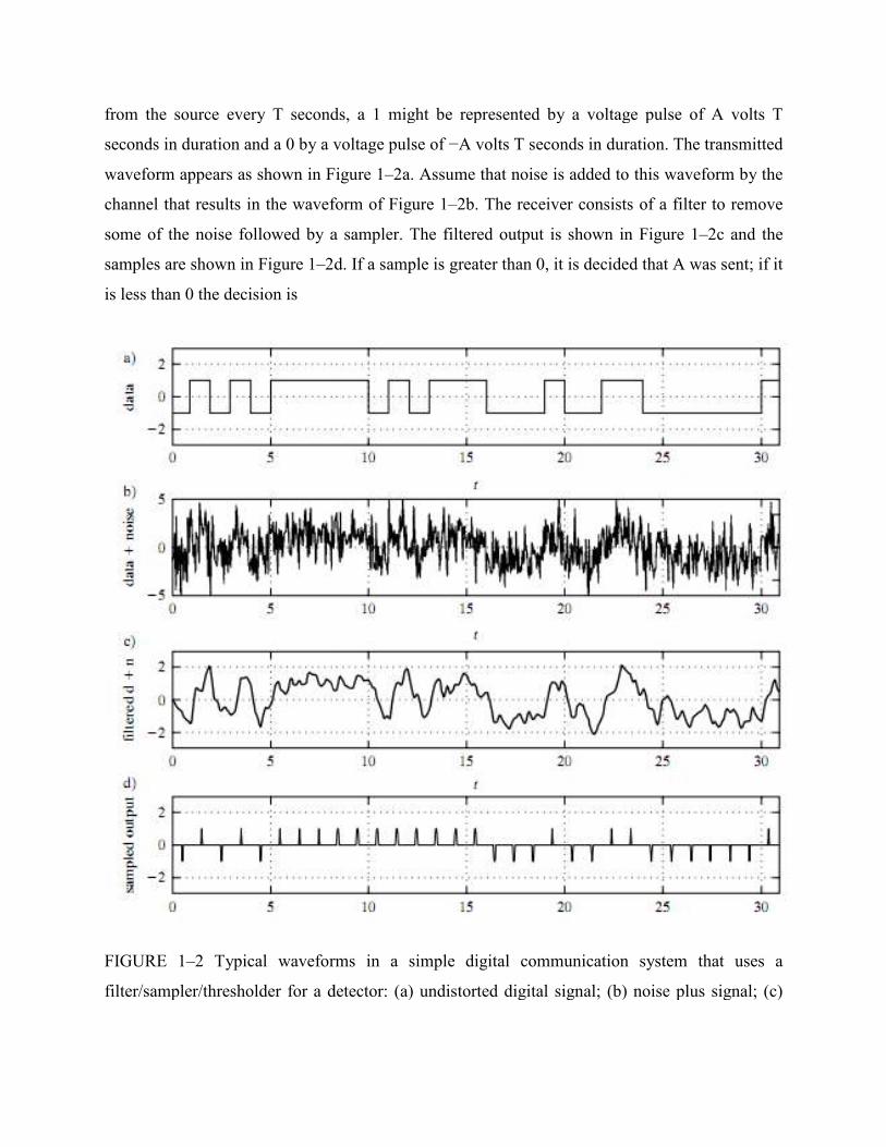
from the source every T seconds, a 1 might be represented by a voltage pulse of A volts T
seconds in duration and a 0 by a voltage pulse o
waveform appears as shown in Figure 1
channel that results in the waveform of Figure 1
some of the noise followed by a sampler. The filtered output is shown in Figure 1
samples are shown in Figure 1–2d. If a sample is greater than 0, it is decided that A was sent; if it
is less than 0 the decision is
FIGURE 1–2 Typical waveforms in a simple dig
filter/sampler/thresholder for a detector: (a) undistorted digital signal; (b) noise plus signal; (c)
from the source every T seconds, a 1 might be represented by a voltage pulse of A volts T
seconds in duration and a 0 by a voltage pulse of −A volts T seconds in duration. The transmitted
waveform appears as shown in Figure 1–2a. Assume that noise is added to this waveform by the
channel that results in the waveform of Figure 1–2b. The receiver consists of a filter to remove
e followed by a sampler. The filtered output is shown in Figure 1
2d. If a sample is greater than 0, it is decided that A was sent; if it
2 Typical waveforms in a simple digital communication system that uses a
filter/sampler/thresholder for a detector: (a) undistorted digital signal; (b) noise plus signal; (c)
from the source every T seconds, a 1 might be represented by a voltage pulse of A volts T
−A volts T seconds in duration. The transmitted
2a. Assume that noise is added to this waveform by the
2b. The receiver consists of a filter to remove
e followed by a sampler. The filtered output is shown in Figure 1–2c and the
2d. If a sample is greater than 0, it is decided that A was sent; if it
ital communication system that uses a
filter/sampler/thresholder for a detector: (a) undistorted digital signal; (b) noise plus signal; (c)
filtered noisy signal; (d) hard-limited samples of filtered noisy signal—decision = 1 if sample > 0
and −1 if sample < 0. Note the errors resulting from the fairly high noise level.
that a −A was sent. Because of the noise added in the channel, errors may be made in this
decision process. Several are evident in Figure 1–2 upon comparing the top waveform with the
samples in the bottom plot. The synchronization required to sample at the proper instant is no
small problem, but will be considered to be carried out ideally in this example. In the next
section, we consider a more detailed block diagram than Figure 1–1 and explain the different
operations that may be encountered in a digital communications system.
1.2 Objectives
At the end of this chapter you will be able to:
• Give brief introduction to Digital Data Transmission.
1.3 Components of a Digital Communications System
The mechanization and performance considerations for digital communications systems
will now be discussed in more detail. Figure 1–3 shows a system block diagram that is more
detailed than that of Figure 1–1. The functions of all the blocks of Figure 1–3 are discussed in
this section.
1.3.1 General Considerations
In most communication system designs, a general objective is to use the resources of
bandwidth and transmitted power as efficiently as possible. In many applications, one of these
resources is scarcer than the other, which results in the classification of most channels as either
bandwidth limited or power limited. Thus we are interested in both a transmission scheme’s
bandwidth efficiency, defined as the ratio of data rate to signal bandwidth, and its power
efficiency, characterized by the probability of making a reception error as a function of signal-to-
noise ratio. We give a preliminary discussion of this power-bandwidth efficiency trade-off in
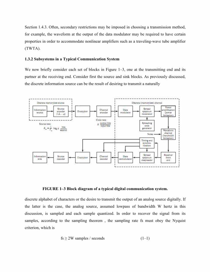
Section 1.4.3. Often, secondary restrictions may
for example, the waveform at the output
properties in order to accommodate
(TWTA).
1.3.2 Subsystems in a Typical Communication System
We now briefly consider each set of blocks in Figure 1
partner at the receiving end. Consider first the source and sink blocks. As previously
the discrete information source can be the result of desiring to transmit a natu
FIGURE 1–3 Block diagram of a typical digital communication system.
discrete alphabet of characters or the desire to transmit the output of an analog source digitally. If
the latter is the case, the analog source, assumed lowpass of bandwidth W hertz i
discussion, is sampled and each sample quantized. In order to recover the signal from its
samples, according to the sampling theorem , the sampling rate fs must obey the Nyquist
criterion, which is
fs ≥ 2W samples / seconds
.3. Often, secondary restrictions may be imposed in choosing a transmission method,
e waveform at the output of the data modulator may be required to have certain
properties in order to accommodate nonlinear amplifiers such as a traveling-wave tube amplifier
.2 Subsystems in a Typical Communication System
r each set of blocks in Figure 1–3, one at the transmitting end and
partner at the receiving end. Consider first the source and sink blocks. As previously
the discrete information source can be the result of desiring to transmit a naturally
3 Block diagram of a typical digital communication system.
discrete alphabet of characters or the desire to transmit the output of an analog source digitally. If
the latter is the case, the analog source, assumed lowpass of bandwidth W hertz i
discussion, is sampled and each sample quantized. In order to recover the signal from its
samples, according to the sampling theorem , the sampling rate fs must obey the Nyquist
≥ 2W samples / seconds (1–1)
be imposed in choosing a transmission method,
of the data modulator may be required to have certain
wave tube amplifier
3, one at the transmitting end and its
partner at the receiving end. Consider first the source and sink blocks. As previously discussed,
rally
3 Block diagram of a typical digital communication system.
discrete alphabet of characters or the desire to transmit the output of an analog source digitally. If
the latter is the case, the analog source, assumed lowpass of bandwidth W hertz in this
discussion, is sampled and each sample quantized. In order to recover the signal from its
samples, according to the sampling theorem , the sampling rate fs must obey the Nyquist
Furthermore, if each sample is quantized into q levels, then log2 q bits are required to represent
each sample value and the minimum source rate in this case is
Rm= (fs )min log 2 q = 2W log2 q bits/ second (1–2)
Consider next the source encoder and decoder blocks in Figure 1–3. Most sources possess
redundancy, manifested by dependencies between successive symbols or by the probabilities of
occurrence of these symbols not being equal, in their outputs. It is therefore possible to represent
a string of symbols, each one being selected from an alphabet of q symbols, from the output of a
redundant source by fewer than log2 q bits per symbol on the average. Thus the function of the
source encoder and decoder blocks in Figure 1–3 is to remove redundancy before transmission
and decode the reduced-redundancy symbols at the receiver, respectively.
It is often desirable to make the transmissions secure from unwanted interceptors. This is the
function of the encryptor and decryptor blocks shown in Figure 1–3. This is true not only in
military applications, but many civilian applications as well (consider the undesirability, for
example, of a competitor learning the details of a competing bid for a construction project that is
being sent to a potential customer by means of a public carrier transmission system). Although
much of the literature on this subject is classified, provides an excellent overview.
In many communications systems, it might not be possible to achieve the level of transmission
reliability desired with the transmitter and receiver parameters available (e.g., power, bandwidth,
receiver sensitivity, and modulation technique). A way to improve performance in many cases is
to encode the transmitted data sequence by adding redundant symbols and using this redundancy
to detect and correct errors at the receiver output. This is the function of the channel
encoder/decoder blocks shown in Figure 1–3. It may seem strange that redundancy is now added
after removing redundancy with the source encoder. This is reasonable, however, since the
channel encoder adds controlled redundancy, which the channel decoder makes use of to correct
errors, whereas the redundancy removed by the source encoder is uncontrolled and is difficult to
make use of in.
1.5 Summary
Data transmitted may be digital messages originating from a data source, for example a computer
or a keyboard. It may also be an analog signal such as a phone call or a video
signal, digitized into a bit-stream for example using pulse-code modulation (PCM) or more
advanced source coding (analog-to-digital conversion and data compression) schemes. This
source coding and decoding is carried out by codec equipment.
1.6 Keywords
• Digital Data Transmission
• Waveform
• FEC
• TWTA
1.7 Exercise
1. Give brief introduction to Digital Data Transmission.
Unit 2
Representation of Data Signal
Structure
2.1 Introduction
2.2 Objectives
2.3 Data
2.4 Signal
2.5 Signal Characteristics
2.6 Digital Signal
2.7 Baseband and Broadband Signals
2.8 Summary
2.9 Keywords
2.10 Exercise
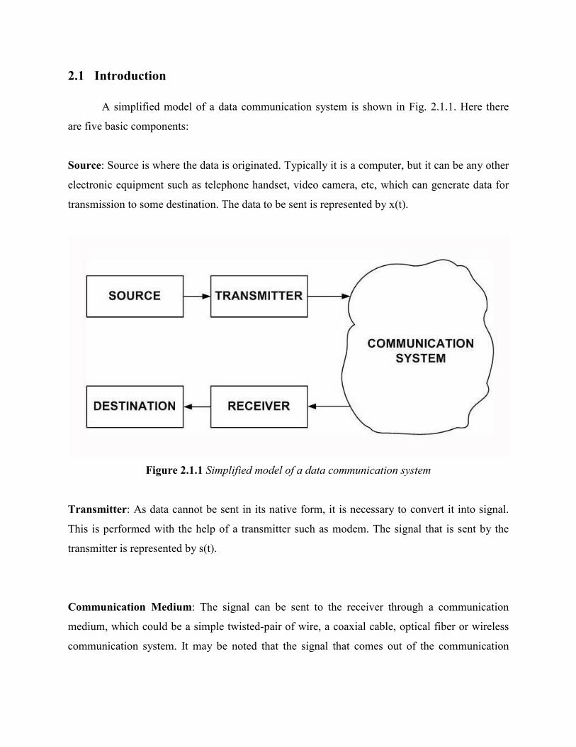
2.1 Introduction
A simplified model of a data communication system is shown in Fig. 2.1.1. Here there
are five basic components:
Source: Source is where the data is originated. Typically it is a computer, but it can be any other
electronic equipment such as telephone handset, video camera, etc, which can generate data for
transmission to some destination. The data to be sent is represented by x(t).
Figure 2.1.1 Simplified model of a data communication system
Transmitter: As data cannot be sent in its native form, it is necessary to convert it into signal.
This is performed with the help of a transmitter such as modem. The signal that is sent by the
transmitter is represented by s(t).
Communication Medium: The signal can be sent to the receiver through a communication
medium, which could be a simple twisted-pair of wire, a coaxial cable, optical fiber or wireless
communication system. It may be noted that the signal that comes out of the communication
medium is s’(t), which is different from s(t) that was sent by the transmitter. This is due to
various impairments that the signal suffers as it passes through the communication medium.
Receiver: The receiver receives the signal s’(t) and converts it back to data d’(t) before
forwarding to the destination. The data that the destination receives may not be identical to that
of d(t), because of the corruption of data.
Destination: Destination is where the data is absorbed. Again, it can be a computer system, a
telephone handset, a television set and so on.
2.2 Objectives
At the end of this chapter you will be able to:
• Explain what is data
• Distinguish between Analog and Digital signal
• Explain the difference between time and Frequency domain representation of signal
• Specify the bandwidth of a signal
• Specify the Sources of impairment
• Explain Attenuation and Unit of Attenuation
• Explain Data Rate Limits and Nyquist Bit Rate
• Distinguish between Bit Rate and Baud Rate
• Identify Noise Sources
2.3 Data
Data refers to information that conveys some meaning based on some mutually agreed up
rules or conventions between a sender and a receiver and today it comes in a variety of forms
such as text, graphics, audio, video and animation.
Data can be of two types; analog and digital. Analog data take on continuous values on some
interval. Typical examples of analog data are voice and video. The data that are collected from
the real world with the help of transducers are continuous-valued or analog in nature. On the
contrary, digital data take on discrete values. Text or character strings can be considered as
examples of digital data. Characters are represented by suitable codes, e.g. ASCII code, where
each character is represented by a 7-bit code.
2.4 Signal
It is electrical, electronic or optical representation of data, which can be sent over a
communication medium. Stated in mathematical terms, a signal is merely a function of the data.
For example, a microphone converts voice data into voice signal, which can be sent over a pair
of wire. Analog signals are continuous-valued; digital signals are discrete-valued. The
independent variable of the signal could be time (speech, for example), space (images), or the
integers (denoting the sequencing of letters and numbers in the football score). Figure 2.1.2
shows an analog signal.
Figure 2.1.2 Analog signal
Digital signal can have only a limited number of defined values, usually two values 0 and 1, as
shown in Fig. 2.1.3.
Figure 2.1.3 Digital signal
Signaling: It is an act of sending signal over communication medium
Transmission: Communication of data by propagation and processing is known as transmission.
2.5 Signal Characteristics
A signal can be represented as a function of time, i.e. it varies with time. However, it can
be also expressed as a function of frequency, i.e. a signal can be considered as a composition of
different frequency components. Thus, a signal has both time-domain and frequency domain
representation.
2.5.1 Time-domain concepts
A signal is continuous over a period, if
limt->a s (t) = s (a), for all a,
i.e., there is no break in the signal. A signal is discrete if it takes on only a finite number of
values. A signal is periodic if and only if
s (t+T) = s (t) for - α < t < α ,
where T is a constant, known as period. The period is measured in seconds.
In other words, a signal is a periodic signal if it completes a pattern within a measurable time
frame. A periodic signal is characterized by the following three parameters.
Amplitude: It is the value of the signal at different instants of time. It is measured in volts.
Frequency: It is inverse of the time period, i.e. f = 1/T. The unit of frequency is Hertz (Hz) or
cycles per second.
Phase: It gives a measure of the relative position in time of two signals within a single period. It
is represented by φ in degrees or radian.
A sine wave, the most fundamental periodic signal, can be completely characterized by its
amplitude, frequency and phase. Examples of sine waves with different amplitude, frequency
and phase are shown in Fig. 2.1.4. The phase angle φ indicated in the figure is with respect to the
reference waveform shown in Fig. 2.1.4(a).
Figure 2.1.4 Examples of signals with different amplitude, frequency and phase
An aperiodic signal or nonperiodic signal changes constantly without exhibiting a pattern or
cycle that repeats over time as shown in Fig. 2.1.5.
Figure 2.1.5
Examples of signals with different amplitude, frequency and phase
or nonperiodic signal changes constantly without exhibiting a pattern or
peats over time as shown in Fig. 2.1.5.
Figure 2.1.5 Examples of aperiodic signals
Examples of signals with different amplitude, frequency and phase
or nonperiodic signal changes constantly without exhibiting a pattern or
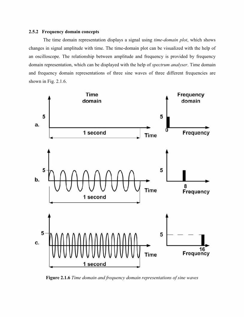
2.5.2 Frequency domain concepts
The time domain representation displays a signal using time-domain plot, which shows
changes in signal amplitude with time. The time-domain plot can be visualized with the help of
an oscilloscope. The relationship between amplitude and frequency is provided by frequency
domain representation, which can be displayed with the help of spectrum analyser. Time domain
and frequency domain representations of three sine waves of three different frequencies are
shown in Fig. 2.1.6.
Figure 2.1.6 Time domain and frequency domain representations of sine waves

Although simple sine waves help us to understand the difference between the time-domain and
frequency domain representation, these are of little use in data communication. Composite
signals made of many simple sine waves find use in data communication. Any composite signal
can be represented by a combination of simple sine waves using Fourier Analysis. For example,
the signal shown in Fig. 2.1.7(c) is a composition of two sine waves having frequencies f1, 3f1,
shown in Fig. 2.1.7 (a) and (b), respectively and it can be represented by
s (t) = sin ωt + 1/3 sin 3ωt , where ω = 2πf1.
The frequency domain function s(f) specifies the constituent frequencies of the signal. The range
of frequencies that a signal contains is known as it spectrum, which can be visualized with the
help of a spectrum analyser. The band of frequencies over which most of the energy of a signal is
concentrated is known as the bandwidth of the signal.
Figure 2.1.7 Time and frequency domain representations of a composite signal
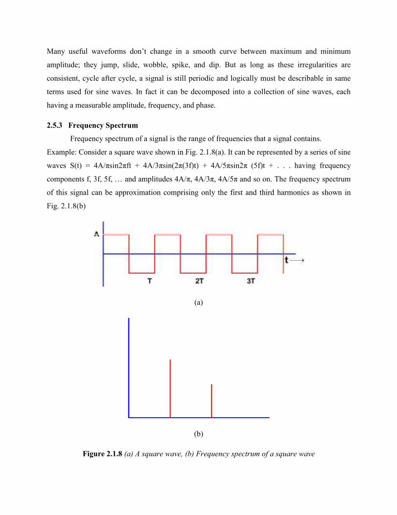
Many useful waveforms don’t change in a smooth curve between maximum and minimum
amplitude; they jump, slide, wobble, spike, and dip. But as long as these irregularities are
consistent, cycle after cycle, a signal is still periodic and logically must be describable in same
terms used for sine waves. In fact it can be decomposed into a collection of sine waves, each
having a measurable amplitude, frequency, and phase.
2.5.3 Frequency Spectrum
Frequency spectrum of a signal is the range of frequencies that a signal contains.
Example: Consider a square wave shown in Fig. 2.1.8(a). It can be represented by a series of sine
waves S(t) = 4A/πsin2πft + 4A/3πsin(2π(3f)t) + 4A/5πsin2π (5f)t + . . . having frequency
components f, 3f, 5f, … and amplitudes 4A/π, 4A/3π, 4A/5π and so on. The frequency spectrum
of this signal can be approximation comprising only the first and third harmonics as shown in
Fig. 2.1.8(b)
(a)
(b)
Figure 2.1.8 (a) A square wave, (b) Frequency spectrum of a square wave
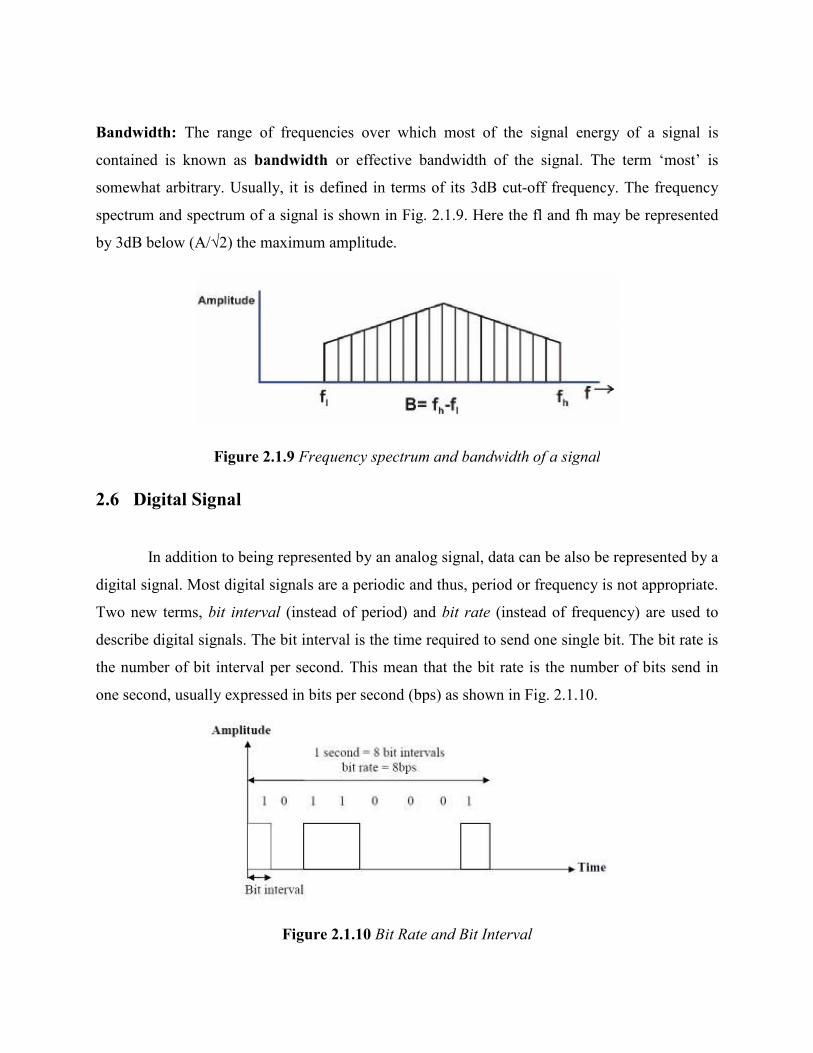
Bandwidth: The range of freque
contained is known as bandwidth
somewhat arbitrary. Usually, it is defined in terms of its 3dB cut
spectrum and spectrum of a signal is shown in Fig. 2.1.9. Here the fl and fh may be represented
by 3dB below (A/√2) the maximum amplitude.
Figure 2.1.9 Frequency spectrum and bandwidth of a signal
2.6 Digital Signal
In addition to being represented by an analog signal, data can be also be represented by a
digital signal. Most digital signals are a
Two new terms, bit interval (instead of period) and
describe digital signals. The bit interval is the time required to send one single bit. The bit rate is
the number of bit interval per second. This mean that the bit rate is the number of bits send in
one second, usually expressed in bits per second (bps) as shown in Fig. 2.1.10.
Figure 2.1.10
The range of frequencies over which most of the signal energy of a signal is
bandwidth or effective bandwidth of the signal. The term ‘most’ is
somewhat arbitrary. Usually, it is defined in terms of its 3dB cut-off frequency. The frequency
spectrum of a signal is shown in Fig. 2.1.9. Here the fl and fh may be represented
2) the maximum amplitude.
Frequency spectrum and bandwidth of a signal
In addition to being represented by an analog signal, data can be also be represented by a
digital signal. Most digital signals are a periodic and thus, period or frequency is not appropriate.
(instead of period) and bit rate (instead of frequency) are used to
describe digital signals. The bit interval is the time required to send one single bit. The bit rate is
the number of bit interval per second. This mean that the bit rate is the number of bits send in
expressed in bits per second (bps) as shown in Fig. 2.1.10.
Figure 2.1.10 Bit Rate and Bit Interval
ncies over which most of the signal energy of a signal is
or effective bandwidth of the signal. The term ‘most’ is
off frequency. The frequency
spectrum of a signal is shown in Fig. 2.1.9. Here the fl and fh may be represented
In addition to being represented by an analog signal, data can be also be represented by a
periodic and thus, period or frequency is not appropriate.
(instead of frequency) are used to
describe digital signals. The bit interval is the time required to send one single bit. The bit rate is
the number of bit interval per second. This mean that the bit rate is the number of bits send in
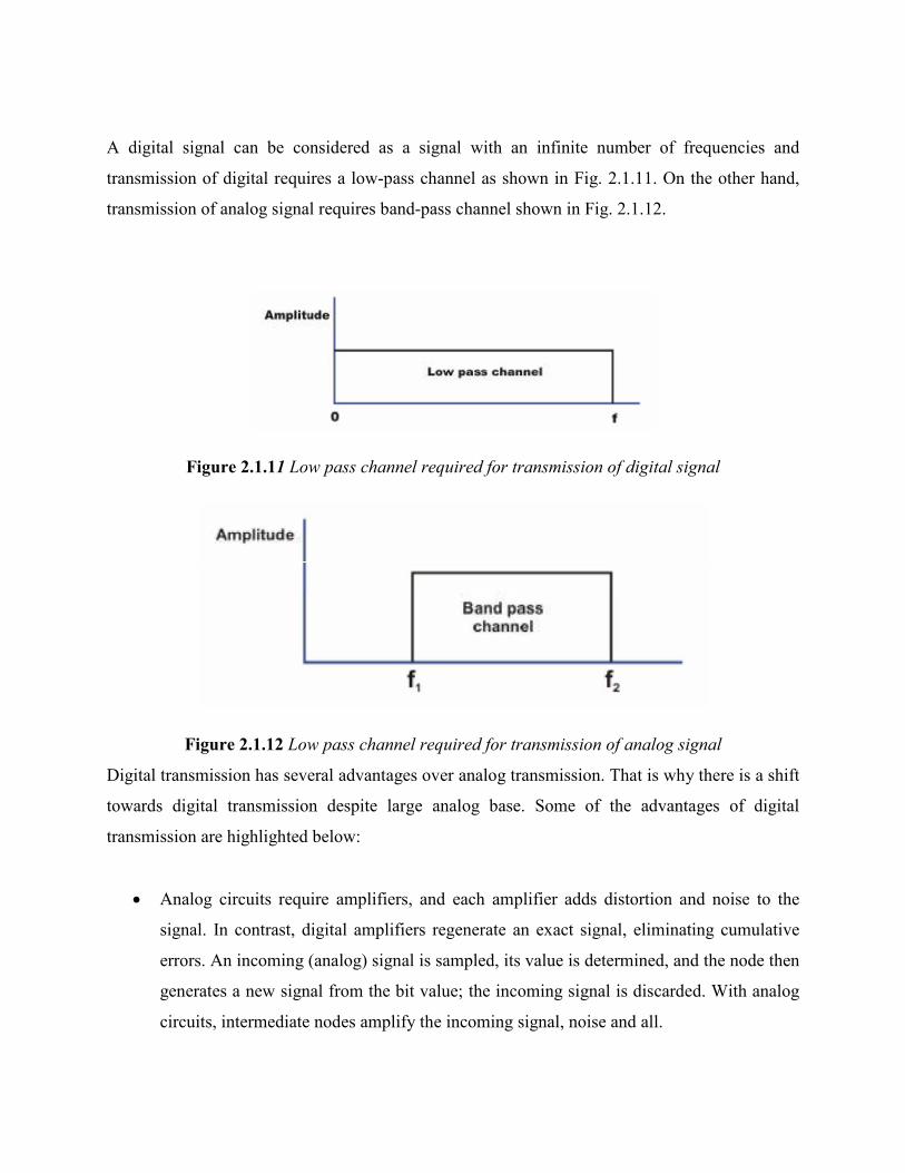
A digital signal can be considered as a signal with an infinite number of frequencies and
transmission of digital requires a low-pass channel as shown in Fig. 2.1.11. On the other hand,
transmission of analog signal requires band-pass channel shown in Fig. 2.1.12.
Figure 2.1.11 Low pass channel required for transmission of digital signal
Figure 2.1.12 Low pass channel required for transmission of analog signal
Digital transmission has several advantages over analog transmission. That is why there is a shift
towards digital transmission despite large analog base. Some of the advantages of digital
transmission are highlighted below:
• Analog circuits require amplifiers, and each amplifier adds distortion and noise to the
signal. In contrast, digital amplifiers regenerate an exact signal, eliminating cumulative
errors. An incoming (analog) signal is sampled, its value is determined, and the node then
generates a new signal from the bit value; the incoming signal is discarded. With analog
circuits, intermediate nodes amplify the incoming signal, noise and all.
• Voice, data, video, etc. can all by carried by digital circuits. What about carrying digital
signals over analog circuit? The modem example shows the difficulties in carrying digital
over analog. A simple encoding method is to use constant voltage levels for a “1'' and a
``0''. Can lead to long periods where the voltage does not change.
• Easier to multiplex large channel capacities with digital.
• Easy to apply encryption to digital data.
• Better integration if all signals are in one form. Can integrate voice, video and digital
data.
2.7 Baseband and Broadband Signals
Depending on some type of typical signal formats or modulation schemes, a few
terminologies evolved to classify different types of signals. So, we can have either a base band or
broadband signalling. Base-band is defined as one that uses digital signalling, which is inserted
in the transmission channel as voltage pulses. On the other hand, broadband systems are those,
which use analog signalling to transmit information using a carrier of high frequency.
In baseband LANs, the entire frequency spectrum of the medium is utilized for transmission and
hence the frequency division multiplexing (discussed later) cannot be used. Signals inserted at a
point propagates in both the directions, hence transmission is bi-directional. Baseband systems
extend only to limited distances because at higher frequency, the attenuation of the signal is most
pronounced and the pulses blur out, causing the large distance communication totally
impractical.
Since broadband systems use analog signalling, frequency division multiplexing is possible,
where the frequency spectrum of the cable is divided into several sections of bandwidth. These
separate channels can support different types of signals of various frequency ranges to travel at
the same instance. Unlike base-band, broadband is a unidirectional medium where the signal
inserted into the media propagates in only one direction. Two data paths are required, which are
connected at a point in the network called headend. All the stations transmit towards the headend
on one path and the signals received at the headend are propagated through the second path.
2.8 Summary
Data refers to information that conveys some meaning based on some mutually agreed up
rules or conventions between a sender and a receiver and today it comes in a variety of forms
such as text, graphics, audio, video and animation. It is electrical, electronic or optical
representation of data, which can be sent over a communication medium.
A signal can be represented as a function of time, i.e. it varies with time. However, it can
be also expressed as a function of frequency, i.e. a signal can be considered as a composition of
different frequency components. Thus, a signal has both time-domain and frequency domain
representation.
2.9 Keywords
• Source
• Transmitter
• Communication Medium
• Receiver
• Destination
• Signal
• Amplitude
• Frequency
• Phase
2.10 Exercise
1. Distinguish between data and signal.
2. What do you mean by a “Periodic Signal”? And what are the three parameters that
characterize it?
3. Distinguish between time domain and frequency domain representation of a signal.
4. What equipments are used to visualize electrical signals in time domain and frequency
domain?
5. What do you mean by the Bit Interval and Bit rate in a digital signal?
Unit 3
Digital Data Transmission-1
Structure
3.1 Introduction
3.2 Objectives
3.3 Parallel and Serial Data Transmission
3.4 20ma Loop and Line Drivers
3.5 Modems
3.6 Summary
3.7 Keywords
3.8 Exercise
3.1 Introduction
The transmission mode refers to the number of elementary units of information (bits)
that can be simultaneously translated by the communications channel. In fact, processors (and
therefore computers in general) never process (in the case of recent processors) a single bit at a
time; generally they are able to process several (most of the time it is 8: one byte), and for this
reason the basic connections on a computer are parallel connections.
3.2 Objectives
At the end of this chapter you will be able to:
• Know the Parallel and Serial Data Transmission.
• Explain 20ma Loop And Line Drivers.
• Know how Modem works.
3.3 Parallel and Serial Data Transmission
Digital data transmission can occur in two basic modes: serial or parallel. Data within
a computer system is transmitted via parallel mode on buses with the width of the parallel
bus matched to the word size of the computer system. Data between computer systems is usually
transmitted in bit serial mode. Consequently, it is necessary to make a parallel-to-serial
conversion at a computer interface when sending data from a computer system into a network
and a serial-to-parallel conversion at a computer interface when receiving information from a
network. The type of transmission mode used may also depend upon distance and required data
rate.
Parallel Transmission
In parallel transmission, multiple bits (usually 8 bits or a byte/character) are sent simultaneously
on different channels (wires, frequency channels) within the same cable, or radio path,
and synchronized to a clock. Parallel devices have a wider data bus than serial devices and can
therefore transfer data in words of one or more bytes at a time. As a result, there is a speedup in
parallel transmission bit rate over serial transmission bit rate. However, this speedup is a tradeoff
versus cost since multiple wires cost more than a single wire, and as a parallel cable gets longer,
the synchronization timing between multiple channels becomes more sensitive to distance.
The timing for parallel transmission is provided by a constant clocking signal sent over a
separate wire within the parallel cable; thus parallel transmission is considered synchronous.
Serial Transmission
In serial transmission, bits are sent sequentially on the same channel (wire) which reduces
costs for wire but also slows the speed of transmission. Also, for serial transmission, some
overhead time is needed since bits must be assembled and sent as a unit and then disassembled at
the receiver.
Serial transmission can be either synchronous or asynchronous. In synchronous transmission,
groups of bits are combined into frames and frames are sent continuously with or without data to
be transmitted. In asynchronous transmission, groups of bits are sent as independent units with
start/stop flags and no data link synchronization, to allow for arbitrary size gaps between frames.
However, start/stop bits maintain physical bit level synchronization once detected.
Applications
Serial transmission is between two computers or from a computer to an external device located
some distance away. Parallel transmission either takes place within a computer system (on a
computer bus) or to an external device located a close distance away.
A special computer chip known as a universal asynchronous receiver transmitter (UART) acts as
the interface between the parallel transmission of the computer bus and the serial transmission of
the serial port. UARTs differ in performance capabilities based on the amount of on-chip
memory they possess.
Examples
Examples of parallel mode transmission include connections between a computer and a printer
(parallel printer port and cable). Most printers are within6 meters or 20 feet of the transmitting
computer and the slight cost for extra wires is offset by the added speed gained through
parallel transmission of data.
Examples of serial mode transmission include connections between a computer and a modem
using the RS-232 protocol. Although an RS-232 cable can theoretically accommodate 25 wires,
all but two of these wires are for overhead control signaling and not data transmission; the two
data wires perform simple serial transmission in either direction. In this case, a computer may
not be close to a modem, making the cost of parallel transmission prohibitive—thus speed
of transmission may be considered less important than the economical advantage of
serial transmission.
Tradeoffs
Serial transmission via RS-232 is officially limited to 20 Kbps for a distance of 15 meters or 50
feet. Depending on the type of media used and the amount of external interference present, RS-
232 can be transmitted at higher speeds, or over greater distances, or both.
Parallel transmission has similar distance-versus-speed tradeoffs, as well as a clocking threshold
distance. Techniques to increase the performance of serial and parallel transmission (longer
distance for same speed or higher speed for same distance) include using
better transmission media, such as fiber optics or conditioned cables, implementing repeaters, or
using shielded/multiple wires for noise immunity.
Technology
To resolve the speed and distance limitations of serial transmission via RS-232, several other
serial transmission standards have been developed including RS-449, V.35, Universal Serial Bus
(USB), and IEEE-1394 (Fire wire). Each of these standards has different electrical, mechanical,
functional, and procedural characteristics. The electrical characteristics define voltage levels
and timing of voltage level changes. Mechanical characteristics define the actual connector shape
and number of wires. Common mechanical interface standards associated with
parallel transmission are the DB-25 and Centronics connectors. The Centronics connector is a
36-pin parallel interface that also defines electrical signaling. Functional characteristics specify
the operations performed by each pin in a connector; these can be classified into the broad
categories of data, control, timing, and electrical ground. The procedural characteristics or
protocol define the sequence of operations performed by pins in the connector.
3.4 20ma Loop and Line Drivers
For digital serial communications, a current loop is a communication interface that
uses current instead of voltage for signaling. Current loops can be used over moderately long
distances (tens of kilo metres), and can be interfaced with optically isolated links.
Long before the RS-232 standard, current loops were used to send digital data
in serial form for teleprinters. More than two teletypes could be connected on a single circuit
allowing a simple form of networking. Older teletypes used a 60 mA current loop. Later
machines, such as the ASR33 teleprinter, operated on a lower 20 mA current level and most
early minicomputers featured a 20 mA current loop interface, with an RS-232 port generally
available as a more expensive option. The original IBM PC serial port card had provisions for a
20 mA current loop. A digital current loop uses the absence of current for high (space or break),
and the presence of current in the loop for low (mark).
The maximum resistance for a current loop is limited by the available voltage. Current
loop interfaces usually use voltages much higher than those found on anRS-232 interface, and
cannot be interconnected with voltage-type inputs without some form of level translator circuit.
MIDI (Musical Instrument Digital Interface) is a digital current loop interface.
Process Control use
For industrial process control instruments, analog 4–20 mA and 10–50 mA current loops
are commonly used for analog signaling, with 4 mA representing the lowest end of the range and
20 mA the highest. The key advantages of the current loop are that the accuracy of the signal is
not affected by voltage drop in the interconnecting wiring, and that the loop can supply operating
power to the device. Even if there is significant electrical resistance in the line, the current loop
transmitter will maintain the proper current, up to its maximum voltage capability. The live-
zero represented by 4 mA allows the receiving instrument to detect some failures of the loop, and
also allows transmitter devices to be powered by the same current loop (called two-
wire transmitters). Such instruments are used to measure pressure, temperature, flow, pH or other
process variables. A current loop can also be used to control a valve positioner or other
output actuator. An analog current loop can be converted to a voltage input with a precision
resistor. Since input terminals of instruments may have one side of the current loop input tied to
the chassis ground (earth), analog isolators may be required when connecting several instruments
in series.
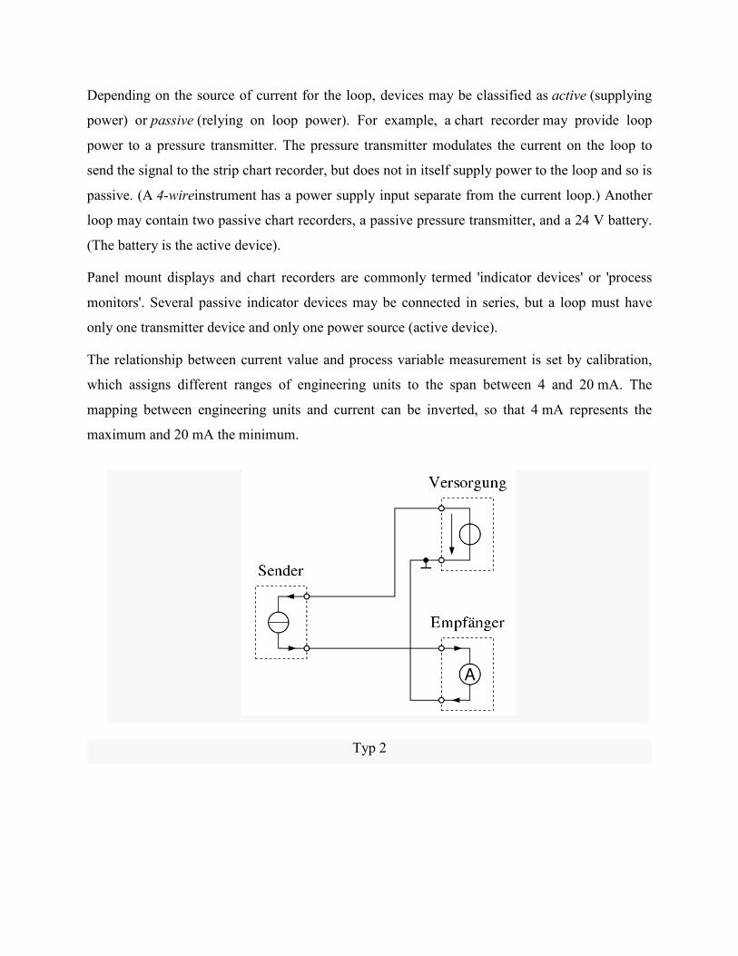
Depending on the source of current for the loop
power) or passive (relying on loop power). For example, a
power to a pressure transmitter. The pr
send the signal to the strip chart recorder, but does not in itself supply power to the loop and so is
passive. (A 4-wireinstrument has a power supply input separate from the current loop.) Another
loop may contain two passive chart recorders, a passive pressure transmitter, and a 24 V battery.
(The battery is the active device).
Panel mount displays and chart recorders are commonly termed 'indicator devices' or 'process
monitors'. Several passive indicator devices may be connected in series, but a loop must have
only one transmitter device and only one power source (active device).
The relationship between current value and process variable measurement is set by calibration,
which assigns different ranges of engineering units to the span between 4 and 20
mapping between engineering units and current can be inverted, so that 4
maximum and 20 mA the minimum.
Depending on the source of current for the loop, devices may be classified as active
(relying on loop power). For example, a chart recorder may provide loop
power to a pressure transmitter. The pressure transmitter modulates the current on the loop to
send the signal to the strip chart recorder, but does not in itself supply power to the loop and so is
instrument has a power supply input separate from the current loop.) Another
op may contain two passive chart recorders, a passive pressure transmitter, and a 24 V battery.
(The battery is the active device).
Panel mount displays and chart recorders are commonly termed 'indicator devices' or 'process
cator devices may be connected in series, but a loop must have
only one transmitter device and only one power source (active device).
The relationship between current value and process variable measurement is set by calibration,
ges of engineering units to the span between 4 and 20
mapping between engineering units and current can be inverted, so that 4 mA represents the
mA the minimum.
Typ 2
active (supplying
may provide loop
essure transmitter modulates the current on the loop to
send the signal to the strip chart recorder, but does not in itself supply power to the loop and so is
instrument has a power supply input separate from the current loop.) Another
op may contain two passive chart recorders, a passive pressure transmitter, and a 24 V battery.
Panel mount displays and chart recorders are commonly termed 'indicator devices' or 'process
cator devices may be connected in series, but a loop must have
The relationship between current value and process variable measurement is set by calibration,
ges of engineering units to the span between 4 and 20 mA. The
mA represents the
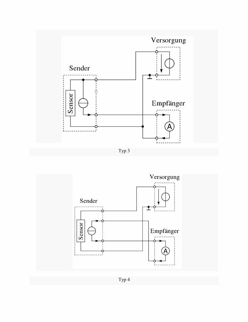
Typ 3
Typ 4
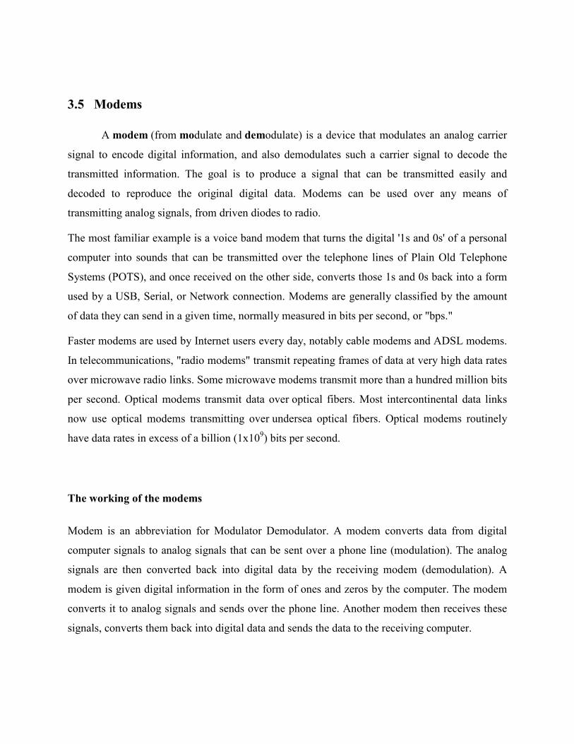
3.5 Modems
A modem (from modulate and demodulate) is a device that modulates an analog carrier
signal to encode digital information, and also demodulates such a carrier signal to decode the
transmitted information. The goal is to produce a signal that can be transmitted easily and
decoded to reproduce the original digital data. Modems can be used over any means of
transmitting analog signals, from driven diodes to radio.
The most familiar example is a voice band modem that turns the digital '1s and 0s' of a personal
computer into sounds that can be transmitted over the telephone lines of Plain Old Telephone
Systems (POTS), and once received on the other side, converts those 1s and 0s back into a form
used by a USB, Serial, or Network connection. Modems are generally classified by the amount
of data they can send in a given time, normally measured in bits per second, or "bps."
Faster modems are used by Internet users every day, notably cable modems and ADSL modems.
In telecommunications, "radio modems" transmit repeating frames of data at very high data rates
over microwave radio links. Some microwave modems transmit more than a hundred million bits
per second. Optical modems transmit data over optical fibers. Most intercontinental data links
now use optical modems transmitting over undersea optical fibers. Optical modems routinely
have data rates in excess of a billion (1x10⁹) bits per second.
The working of the modems
Modem is an abbreviation for Modulator Demodulator. A modem converts data from digital
computer signals to analog signals that can be sent over a phone line (modulation). The analog
signals are then converted back into digital data by the receiving modem (demodulation). A
modem is given digital information in the form of ones and zeros by the computer. The modem
converts it to analog signals and sends over the phone line. Another modem then receives these
signals, converts them back into digital data and sends the data to the receiving computer.
The actual process is much more complicated then it seems. Here we discuss some internal
functions of modem that helps in the modulation and demodulation process.
1. Data Compression
Computers are capable of transmitting information to modems much faster than the modems are
able to transmit the same information over a phone line. However, in order to transmit data at a
speed greater than 600 bits per second (bps), it is necessary for modems to collect bits of
information together and transmit them via a more complicated sound. This allows the
transmission of many bits of data at the same time. This gives the modem time to group bits
together and apply compression algorithms to them. Modem compresses them and sends over.
2. Error Correction
Error correction is the method by which modems verify if the information sent to them has been
undamaged during the transfer. Error correcting modems break up information into small
packets, called frames and send over after adding a checksum to each of these frames. The
receiving modem checks whether the checksum matches the information sent. If not, the entire
frame is resent. Though error correction data transfer integrity is preserved.
3. Flow Control
If one modem in a dial up connection is capable of sending data much faster than the other can
receive then flow control allows the receiving modem to tell the other to pause while it catches
up. Flow control exists as either software or hardware flow control. With software flow control,
when a modem needs to tell the other to pause, it sends a certain character signaling pause. When
it is ready to resume, it sends a different character. Since software flow control regulates
transmissions by sending certain characters, line noise could generate the character commanding
a pause, thus hanging the transfer until the proper character is sent. Hardware flow control uses
wires in the modem cable. This is faster and much more reliable than software flow control.
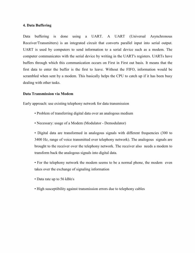
4. Data Buffering
Data buffering is done using a UART. A UART (Universal Asynchronous
Receiver/Transmitters) is an integrated circuit that converts parallel input into serial output.
UART is used by computers to send information to a serial device such as a modem. The
computer communicates with the serial device by writing in the UART's registers. UARTs have
buffers through which this communication occurs on First in First out basis. It means that the
first data to enter the buffer is the first to leave. Without the FIFO, information would be
scrambled when sent by a modem. This basically helps the CPU to catch up if it has been busy
dealing with other tasks.
Data Transmission via Modem
Early approach: use existing telephony network for data transmission
• Problem of transferring digital data over an analogous medium
• Necessary: usage of a Modem (Modulator - Demodulator)
• Digital data are transformed in analogous signals with different frequencies (300 to
3400 Hz, range of voice transmitted over telephony network). The analogous signals are
brought to the receiver over the telephony network. The receiver also needs a modem to
transform back the analogous signals into digital data.
• For the telephony network the modem seems to be a normal phone, the modem even
takes over the exchange of signaling information
• Data rate up to 56 kBit/s
• High susceptibility against transmission errors due to telephony cables
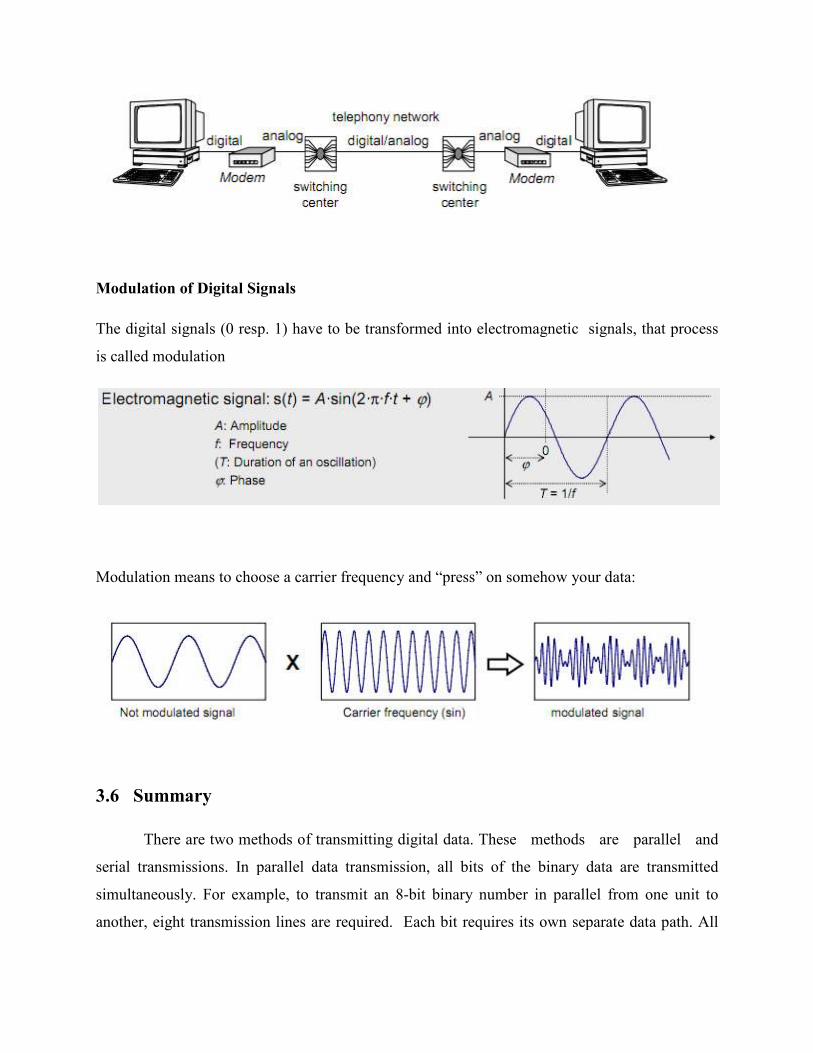
Modulation of Digital Signals
The digital signals (0 resp. 1) have to be transformed into electromagnetic signals, that process
is called modulation
Modulation means to choose a carrier frequency and “press”
3.6 Summary
There are two methods of transmitting digital
serial transmissions. In parallel data transmission, all bits of the binary data are transmitted
simultaneously. For example, to transmit an 8
another, eight transmission lines are required
The digital signals (0 resp. 1) have to be transformed into electromagnetic signals, that process
Modulation means to choose a carrier frequency and “press” on somehow your data:
There are two methods of transmitting digital data. These methods are parallel and
serial transmissions. In parallel data transmission, all bits of the binary data are transmitted
, to transmit an 8-bit binary number in parallel from one unit to
lines are required. Each bit requires its own separate
The digital signals (0 resp. 1) have to be transformed into electromagnetic signals, that process
on somehow your data:
data. These methods are parallel and
serial transmissions. In parallel data transmission, all bits of the binary data are transmitted
parallel from one unit to
Each bit requires its own separate data path. All
bits of a word are transmitted at the same time. This method of transmission can move a
significant amount of data in a given period of time. Its disadvantage is the large number
of interconnecting cables between the two units. For large binary words, cabling becomes
complex and expensive. This is particularly true if the distance between the two units is great.
Long multi wire cables are not only expensive, but also require special interfacing to minimize
noise and distortion problems. The 4-2OmA current loop has been with us for so long that it's
become rather taken for granted in the industrial and process sectors alike. Its popularity comes
from its ease of use and its performance. However, just because something is that ubiquitous
doesn't mean we're all necessarily getting the best out of our current loops.
3.7 Keywords
• Modem
• Buses
• Bits
• Serial Transmission
• Modulate
• Demodulate
• Flow Control
3.8 Exercise
1. Explain the Parallel and Serial Data Transmission.
2. Explain 20ma Loop And Line Drivers.
3. Explain the working of Modem.
Unit 4
Digital Data Transmission-2
Structure
4.1 Introduction
4.2 Objectives
4.3 Transient Noise Pulses
4.4 Data Signal: Signal Shaping And Signaling Speed
4.5 Partial Response (Correlative) Techniques
4.6 Repeaters
4.7 Summary
4.8 Keywords
4.9 Exercise
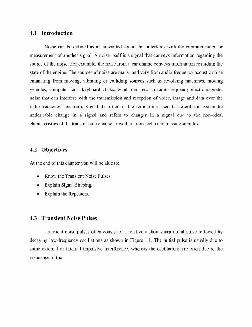
4.1 Introduction
Noise can be defined as an unwanted signal that interferes with the communication or
measurement of another signal. A noise itself is a signal that conveys information regarding the
source of the noise. For example, the noise from a car engine conveys information regarding the
state of the engine. The sources of noise are many, and vary from audio frequency acoustic noise
emanating from moving, vibrating or colliding sources such as revolving machines, moving
vehicles, computer fans, keyboard clicks, wind, rain, etc. to radio-frequency electromagnetic
noise that can interfere with the transmission and reception of voice, image and data over the
radio-frequency spectrum. Signal distortion is the term often used to describe a systematic
undesirable change in a signal and refers to changes in a signal due to the non–ideal
characteristics of the transmission channel, reverberations, echo and missing samples.
4.2 Objectives
At the end of this chapter you will be able to:
• Know the Transient Noise Pulses.
• Explain Signal Shaping.
• Explain the Repeaters.
4.3 Transient Noise Pulses
Transient noise pulses often consist of a relatively short sharp initial pulse followed by
decaying low-frequency oscillations as shown in Figure 1.1. The initial pulse is usually due to
some external or internal impulsive interference, whereas the oscillations are often due to the
resonance of the
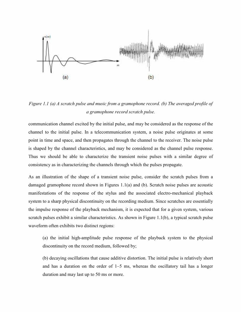
Figure 1.1 (a) A scratch pulse and music from a gramophone record. (b) The averaged profile of
a gramophone record scratch
communication channel excited by the initial pulse, and may be considered as the response of the
channel to the initial pulse. In a telecommunication system, a noise pulse originates at some
point in time and space, and then propagates through the c
is shaped by the channel characteristics, and may be considered as the channel pulse response.
Thus we should be able to characterize the transient noise pulses with a similar degree of
consistency as in characterizing the channels through which the pulses propagate.
As an illustration of the shape of a transient noise pulse, consider the scratch pulses from a
damaged gramophone record shown in Figures 1.1(a) and (b). Scratch noise pulses are acoustic
manifestations of the response of the stylus and the associated electro
system to a sharp physical discontinuity on the recording medium. Since scratches are essentially
the impulse response of the playback mechanism, it is expected that for a given s
scratch pulses exhibit a similar characteristics. As shown in Figure 1.1(b), a typical scratch pulse
waveform often exhibits two distinct regions:
(a) the initial high-amplitude pulse response of the playback system to the physical
discontinuity on the record medium, followed by;
(b) decaying oscillations that cause additive distortion. The initial pulse is relatively short
and has a duration on the order of 1
duration and may last up to 50
Figure 1.1 (a) A scratch pulse and music from a gramophone record. (b) The averaged profile of
a gramophone record scratch pulse.
communication channel excited by the initial pulse, and may be considered as the response of the
channel to the initial pulse. In a telecommunication system, a noise pulse originates at some
point in time and space, and then propagates through the channel to the receiver. The noise pulse
is shaped by the channel characteristics, and may be considered as the channel pulse response.
Thus we should be able to characterize the transient noise pulses with a similar degree of
ng the channels through which the pulses propagate.
As an illustration of the shape of a transient noise pulse, consider the scratch pulses from a
damaged gramophone record shown in Figures 1.1(a) and (b). Scratch noise pulses are acoustic
of the response of the stylus and the associated electro-mechanical playback
system to a sharp physical discontinuity on the recording medium. Since scratches are essentially
the impulse response of the playback mechanism, it is expected that for a given s
scratch pulses exhibit a similar characteristics. As shown in Figure 1.1(b), a typical scratch pulse
waveform often exhibits two distinct regions:
amplitude pulse response of the playback system to the physical
inuity on the record medium, followed by;
(b) decaying oscillations that cause additive distortion. The initial pulse is relatively short
and has a duration on the order of 1–5 ms, whereas the oscillatory tail has a longer
duration and may last up to 50 ms or more.
Figure 1.1 (a) A scratch pulse and music from a gramophone record. (b) The averaged profile of
communication channel excited by the initial pulse, and may be considered as the response of the
channel to the initial pulse. In a telecommunication system, a noise pulse originates at some
hannel to the receiver. The noise pulse
is shaped by the channel characteristics, and may be considered as the channel pulse response.
Thus we should be able to characterize the transient noise pulses with a similar degree of
ng the channels through which the pulses propagate.
As an illustration of the shape of a transient noise pulse, consider the scratch pulses from a
damaged gramophone record shown in Figures 1.1(a) and (b). Scratch noise pulses are acoustic
mechanical playback
system to a sharp physical discontinuity on the recording medium. Since scratches are essentially
the impulse response of the playback mechanism, it is expected that for a given system, various
scratch pulses exhibit a similar characteristics. As shown in Figure 1.1(b), a typical scratch pulse
amplitude pulse response of the playback system to the physical
(b) decaying oscillations that cause additive distortion. The initial pulse is relatively short
5 ms, whereas the oscillatory tail has a longer
Note in Figure 1.1(b) that the frequency of the decaying oscillations decreases with time. This
behaviour may be attributed to the non-linear modes of response of the electro-mechanical
playback system excited by the physical scratch discontinuity. Observations of many scratch
waveforms from damaged gramophone records reveals that they have a well-defined profile, and
can be characterised by a relatively small number of typical templates.
4.4 Data Signal: Signal Shaping and Signaling Speed
In digital telecommunication, pulse shaping is the process of changing the waveform of
transmitted pulses. Its purpose is to make the transmitted signal better suited to
the communication channel by limiting the effective bandwidth of the transmission. By filtering
the transmitted pulses this way, the inter symbol interference caused by the channel can be kept
in control. In RF communication, pulse shaping is essential for making the signal fit in its
frequency band.
Need for pulse shaping
Transmitting a signal at high modulation rate through a band-limited channel can
create intersymbol interference. As the modulation rate increases, the signal's bandwidth
increases. When the signal's bandwidth becomes larger than the channel bandwidth, the channel
starts to introduce distortion to the signal. This distortion is usually seen as intersymbol
interference.
The signal's spectrum is determined by the pulse shaping filter used by the transmitter. Usually
the transmitted symbols are represented as a time sequence of dirac delta pulses. This theoretical
signal is then filtered with the pulse shaping filter, producing the transmitted signal. The
spectrum of the transmission is thus determined by the filter.
In many base band communication systems the pulse shaping filter is implicitly a boxcar filter.
Its spectrum is of the form sin(x)/x, and has significant signal power at frequencies higher than
symbol rate. This is not a big problem when optical fibre or even twisted pair cable is used as the
communication channel. However, in RF communications this would waste bandwidth, and only
tightly specified frequency bands are used for single transmissions. In other words, the channel
for the signal is band-limited. Therefore better filters have been developed, which attempt to
minimise the bandwidth needed for a certain symbol rate.
Pulse filters
Not all filters can be used as a pulse shaping filter. The filter itself must not introduce
intersymbol interference — it needs to satisfy certain criteria. Nyquist ISI criterion is commonly
used criterion for evaluation of filters, because it relates the frequency spectrum of the
transmitter signal to intersymbol interference.
Examples of pulse-shaping filters that are commonly found in communication systems are:
The trivial boxcar filter
Sinc shaped filter
Raised-cosine filter
Gaussian filter
Sender side pulse shaping is often combined with a receiver side matched filter to achieve
optimum tolerance for noise in the system. In this case the pulse shaping is equally distributed to
the sender and receiver filters. The filters' amplitude responses are thus point wise square-roots
of the system filters.
Other approaches that eliminate complex pulse shaping filters have been invented. In OFDM, the
carriers are modulated so slowly that each carrier is virtually unaffected by the bandwidth
limitation of the channel.
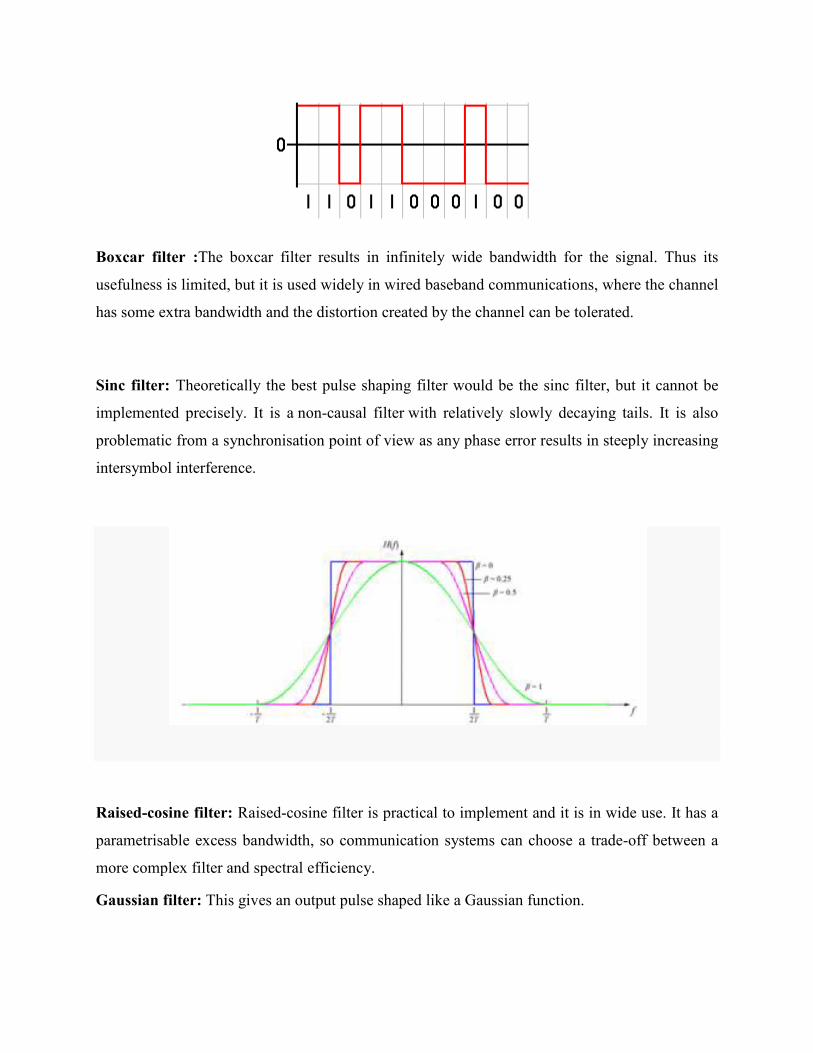
Boxcar filter :The boxcar filter results in infinitely wide bandwidth for the signal. Thus its
usefulness is limited, but it is used widely in wired baseband communications, where the channel
has some extra bandwidth and the distortion created by the channel can be tolerate
Sinc filter: Theoretically the best pulse shaping filter would be the sinc filter, but it cannot be
implemented precisely. It is a non
problematic from a synchronisation point of view as any phase error results in steeply increasing
intersymbol interference.
Raised-cosine filter: Raised-cosine filter is practical to implement and it is in wide use. It has a
parametrisable excess bandwidth, so communication systems can choose a trade
more complex filter and spectral efficiency.
Gaussian filter: This gives an output pulse shaped like a
boxcar filter results in infinitely wide bandwidth for the signal. Thus its
usefulness is limited, but it is used widely in wired baseband communications, where the channel
has some extra bandwidth and the distortion created by the channel can be tolerate
Theoretically the best pulse shaping filter would be the sinc filter, but it cannot be
non-causal filter with relatively slowly decaying tails. It is also
problematic from a synchronisation point of view as any phase error results in steeply increasing
cosine filter is practical to implement and it is in wide use. It has a
ametrisable excess bandwidth, so communication systems can choose a trade
more complex filter and spectral efficiency.
This gives an output pulse shaped like a Gaussian function.
boxcar filter results in infinitely wide bandwidth for the signal. Thus its
usefulness is limited, but it is used widely in wired baseband communications, where the channel
has some extra bandwidth and the distortion created by the channel can be tolerated.
Theoretically the best pulse shaping filter would be the sinc filter, but it cannot be
ying tails. It is also
problematic from a synchronisation point of view as any phase error results in steeply increasing
cosine filter is practical to implement and it is in wide use. It has a
ametrisable excess bandwidth, so communication systems can choose a trade-off between a
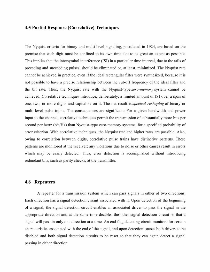
4.5 Partial Response (Correlative) Techniques
The Nyquist criteria for binary and multi-level signaling, postulated in 1924, are based on the
premise that each digit must be confined to its own time slot to as great an extent as possible.
This implies that the intersymbol interference (ISI) in a particular time interval, due to the tails of
preceding and succeeding pulses, should be eliminated or, at least, minimized. The Nyquist rate
cannot be achieved in practice, even if the ideal rectangular filter were synthesized, because it is
not possible to have a precise relationship between the cut-off frequency of the ideal filter and
the bit rate. Thus, the Nyquist rate with the Nyquist-type zero-memory system cannot be
achieved. Correlative techniques introduce, deliberately, a limited amount of ISI over a span of
one, two, or more digits and capitalize on it. The net result is spectral reshaping of binary or
multi-level pulse trains. The consequences are significant: For a given bandwidth and power
input to the channel, correlative techniques permit the transmission of substantially more bits per
second per hertz (b/s/Hz) than Nyquist-type zero-memory systems, for a specified probability of
error criterion. With correlative techniques, the Nyquist rate and higher rates are possible. Also,
owing to correlation between digits, correlative pulse trains have distinctive patterns. These
patterns are monitored at the receiver; any violations due to noise or other causes result in errors
which may be easily detected. Thus, error detection is accomplished without introducing
redundant bits, such as parity checks, at the transmitter.
4.6 Repeaters
A repeater for a transmission system which can pass signals in either of two directions.
Each direction has a signal detection circuit associated with it. Upon detection of the beginning
of a signal, the signal detection circuit enables an associated driver to pass the signal in the
appropriate direction and at the same time disables the other signal detection circuit so that a
signal will pass in only one direction at a time. An end flag detecting circuit monitors for certain
characteristics associated with the end of the signal, and upon detection causes both drivers to be
disabled and both signal detection circuits to be reset so that they can again detect a signal
passing in either direction.
1) In digital communication systems, a repeater is a device that receives
a digital signal on an electromagnetic or optical transmission medium and regenerates the
signal along the next leg of the medium. In electromagnetic media, repeaters overcome
the attenuationcaused by free-space electromagnetic-field divergence or cable loss. A
series of repeaters make possible the extension of a signal over a distance.
Repeaters remove the unwanted noise in an incoming signal. Unlike an analog signal, the
original digital signal, even if weak or distorted, can be clearly perceived and restored.
With analog transmission, signals are restrengthened with amplifiers which unfortunately
also amplify noise as well as information.
Because digital signals depend on the presence or absence of voltage, they tend to
dissipate more quickly than analog signals and need more frequent repeating. Whereas
analog signal amplifiers are spaced at 18,000 meter intervals, digital signal repeaters are
typically placed at 2,000 to 6,000 meter intervals.
2) In a wireless communications system, a repeater consists of a radio receiver, an
amplifier, a transmitter, an isolator, and two antennas. The transmitter produces a signal
on a frequency that differs from the received signal. This so-called frequency offset is
necessary to prevent the strong transmitted signal from disabling the receiver. The
isolator provides additional protection in this respect. A repeater, when strategically
located on top of a high building or a mountain, can greatly enhance the performance of a
wireless network by allowing communications over distances much greater than would
be possible without it.
3) In satellite wireless, a repeater (more frequently called a transponder) receives uplink
signals and retransmits them, often on different frequencies, to destination locations.
4) In a cellular telephone system, a repeater is one of a group of transceivers in a
geographic area that collectively serve a system user.
5) In a fiber optic network, a repeater consists of a photocell, an amplifier, and a light-
emitting diode (LED) or infrared-emitting diode (IRED) for each light or IR signal that
requires amplification. Fiber optic repeaters operate at power levels much lower than
wireless repeaters, and are also much simpler and cheaper. However, their design
requires careful attention to ensure that internal circuit noise is minimized.
6) Repeaters are commonly used by commercial and amateur radio operators to extend
signals in the radio frequency range from one receiver to another. These consist of drop
repeaters, similar to the cells in cellular radio, and hub repeaters, which receive and
retransmit signals from and to a number of directions.
7) A bus repeater links one computer bus to a bus in another computer chassis,
essentially chaining one computer to another.
4.7 Summary
In digital telecommunication, pulse shaping is the process of changing the waveform of
transmitted pulses. Its purpose is to make the transmitted signal better suited to
the communication channel by limiting the effective bandwidth of the transmission. By filtering
the transmitted pulses this way, the intersymbol interference caused by the channel can be kept in
control. In RF communication, pulse shaping is essential for making the signal fit in its
frequency band. A repeater for a transmission system which can pass signals in either of two
directions. Each direction has a signal detection circuit associated with it. Upon detection of the
beginning of a signal, the signal detection circuit enables an associated driver to pass the signal
in the appropriate direction and at the same time disables the other signal detection circuit so that
a signal will pass in only one direction at a time.
4.8 Keywords
• Radio-frequency
• Signal Shaping
• Repeaters.
• Pulse shaping
• Pulse filters

4.9 Exercise
1. Explain the Transient Noise Pulses .
2. Explain Signal Shaping.
3. Explain the Repeaters.

Unit 1
Digital Modulation System-1
Structure
1.1 Introduction
1.2 Objectives
1.3 Digital Modulation System
1.4 Phase-shift keying
1.5 Summary
1.6 Keywords
1.7 Exercise
1.1 Introduction
Firstly, what do we mean by digital modulation? Typically the objective of a digital
communication system is to transport digital data between two or more nodes. In radio
communications this is usually achieved by adjusting a physical characteristic of a sinusoidal
carrier, the frequency, phase, amplitude or a combination thereof. This is performed in real
systems with a modulator at the transmitting end to impose the physical change to the carrier and
a demodulator at the receiving end to detect the resultant modulation on reception.
1.2 Objectives
At the end of this chapter you will be able to:
• Explain Digital Modulation System
• Know the Digital Modulation techniques.
• Explain Phase-shift keying.
1.3 Digital Modulation System
The techniques used to modulate digital information so that it can be transmitted via
microwave, satellite or down a cable pair is different to that of analogue transmission. The data
transmitted via satellite or microwave is transmitted as an analogue signal. The techniques used
to transmit analogue signals are used to transmit digital signals. The problem is to convert the
digital signals to a form that can be treated as an analogue signal that is then in the appropriate
form to either be transmitted down a twisted cable pair or applied to the RF stage where is
modulated to a frequency that can be transmitted via microwave or satellite.
The equipment that is used to convert digital signals into analogue format is a modem. The word
modem is made up of the words “modulator” and “demodulator”.
A modem accepts a serial data stream and converts it into an analogue format that matches the
transmission medium.
There are many different modulation techniques that can be utilised in a modem. These
techniques are:
• Amplitude shift key modulation (ASK)
• Frequency shift key modulation (FSK)
• Binary-phase shift key modulation (BPSK)
• Quadrature-phase shift key modulation (QPSK)
• Quadrature amplitude modulation (QAM)
The most common digital modulation techniques are:
1. Phase-shift keying (PSK):
a. Binary PSK (BPSK), using M=2 symbols
b. Quadrature PSK (QPSK), using M=4 symbols
c. Differential PSK (DPSK)
2. Frequency-shift keying (FSK):
a. Audio frequency-shift keying (AFSK)
b. Multi-frequency shift keying (M-ary FSK or MFSK)
3. Amplitude-shift keying (ASK)
4. Quadrature amplitude modulation (QAM) - a combination of PSK and ASK:
5. Wavelet modulation
6. Spread-spectrum techniques:
a. Direct-sequence spread spectrum (DSSS)
b. Chirp spread spectrum (CSS) according to IEEE 802.15.4a CSS uses pseudo-
stochastic coding
c. Frequency-hopping spread spectrum (FHSS) applies a special scheme for channel
release
1.4 Phase-shift keying
Phase-shift keying (PSK) is a digital modulation scheme that conveys data by changing,
or modulating, the phase of a reference signal (the carrier wave).
Any digital modulation scheme uses a finite number of distinct signals to represent digital data.
PSK uses a finite number of phases, each assigned a unique pattern of binary bits. Usually, each
phase encodes an equal number of bits. Each pattern of bits forms the symbol that is represented
by the particular phase. The demodulator, which is designed specifically for the symbol-set used
by the modulator, determines the phase of the received signal and maps it back to the symbol it
represents, thus recovering the original data.
(a) Binary phase-shift keying (BPSK)
BPSK (also sometimes called PRK, Phase Reversal Keying, or 2PSK) is the simplest
form of phase shift keying (PSK). It uses two phases which are separated by 180° and so can also
be termed 2-PSK. It does not particularly matter exactly where the constellation points are
positioned, and in this figure they are shown on the real axis, at 0° and 180°. This modulation is
the most robust of all the PSKs since it takes the highest level of noise or distortion to make the
demodulator reach an incorrect decision. It is, however, only able to modulate at 1 bit/symbol (as
seen in the figure) and so is unsuitable for high data-rate applications when bandwidth is limited.
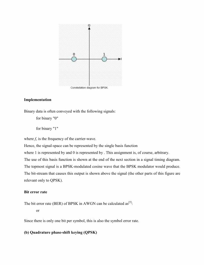
Implementation
Binary data is often conveyed with the following signals:
for binary "0"
for binary "1"
where fc is the frequency of the carrier-wave.
Hence, the signal-space can be represented by the single basis function
where 1 is represented by and 0 is represented by . This assignment is, of course, arbitrary.
The use of this basis function is shown at the end of the next section in a signal timing diagram.
The topmost signal is a BPSK-modulated cosine wave that the BPSK modulator would produce.
The bit-stream that causes this output is shown above the signal (the other parts of this figure are
relevant only to QPSK).
Bit error rate
The bit error rate (BER) of BPSK in AWGN can be calculated as[5]
:
or
Since there is only one bit per symbol, this is also the symbol error rate.
(b) Quadrature phase-shift keying (QPSK)

Constellation diagram for QPSK with Gray coding. Each adjacent symbol only differs by
one bit. Sometimes known as quaternary or quadriphase PSK, 4-PSK, or 4-QAM[6]
, QPSK uses
four points on the constellation diagram, equispaced around a circle. With four phases, QPSK
can encode two bits per symbol. Analysis shows that this may be used either to double the data
rate compared to a BPSK system while maintaining the bandwidth of the signal or to maintain
the data-rate of BPSK but halve the bandwidth needed.
As with BPSK, there are phase ambiguity problems at the receiver and differentially encoded
QPSK is used more often in practice.
Implementation
The implementation of QPSK is more general than that of BPSK and also indicates the
implementation of higher-order PSK. Writing the symbols in the constellation diagram in terms
of the sine and cosine waves used to transmit them:
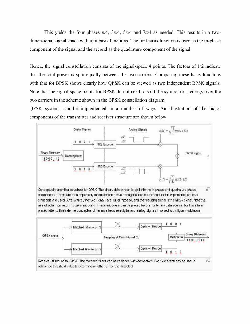
This yields the four phases π/4, 3π/4, 5π/4 and 7π/4 as needed. This results in a two-
dimensional signal space with unit basis functions. The first basis function is used as the in-phase
component of the signal and the second as the quadrature component of the signal.
Hence, the signal constellation consists of the signal-space 4 points. The factors of 1/2 indicate
that the total power is split equally between the two carriers. Comparing these basis functions
with that for BPSK shows clearly how QPSK can be viewed as two independent BPSK signals.
Note that the signal-space points for BPSK do not need to split the symbol (bit) energy over the
two carriers in the scheme shown in the BPSK constellation diagram.
QPSK systems can be implemented in a number of ways. An illustration of the major
components of the transmitter and receiver structure are shown below.
Conceptual transmitter structure for QPSK. The binary data stream is split into the in-
phase and quadrature-phase components. These are then separately modulated onto two
orthogonal basis functions. In this implementation, two sinusoids are used. Afterwards, the two
signals are superimposed, and the resulting signal is the QPSK signal. Note the use of polar non-
return-to-zero encoding. These encoders can be placed before for binary data source, but have
been placed after to illustrate the conceptual difference between digital and analog signals
involved with digital modulation.
Receiver structure for QPSK. The matched filters can be replaced with correlators. Each
detection device uses a reference threshold value to determine whether a 1 or 0 is detected.
Bit error rate
Although QPSK can be viewed as a quaternary modulation, it is easier to see it as two
independently modulated quadrature carriers. With this interpretation, the even (or odd) bits are
used to modulate the in-phase component of the carrier, while the odd (or even) bits are used to
modulate the quadrature-phase component of the carrier. BPSK is used on both carriers and they
can be independently demodulated.
As a result, the probability of bit-error for QPSK is the same as for BPSK:
However, in order to achieve the same bit-error probability as BPSK, QPSK uses twice the
power (since two bits are transmitted simultaneously).
The symbol error rate is given by:
If the signal-to-noise ratio is high (as is necessary for practical QPSK systems) the probability of
symbol error may be approximated:
QPSK signal in the time domain
The modulated signal is shown below for a short segment of a random binary data-stream. The
two carrier waves are a cosine wave and a sine wave, as indicated by the signal-space analysis
above. Here, the odd-numbered bits have been assigned to the in-phase component and the even-
numbered bits to the quadrature component (taking the first bit as number 1). The total signal —
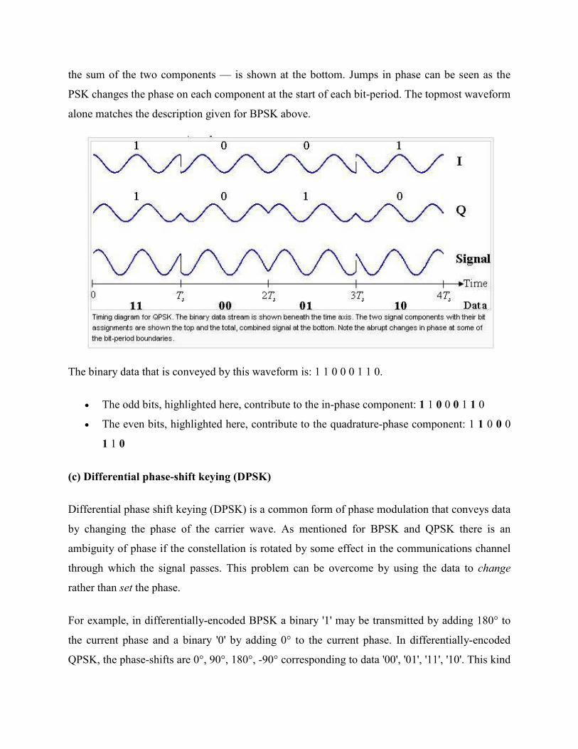
the sum of the two components — is shown at the bottom. Jumps in phase can be seen as the
PSK changes the phase on each component at the start of each bit-period. The topmost waveform
alone matches the description given for BPSK above.
The binary data that is conveyed by this waveform is: 1 1 0 0 0 1 1 0.
• The odd bits, highlighted here, contribute to the in-phase component: 1 1 0 0 0 1 1 0
• The even bits, highlighted here, contribute to the quadrature-phase component: 1 1 0 0 0
1 1 0
(c) Differential phase-shift keying (DPSK)
Differential phase shift keying (DPSK) is a common form of phase modulation that conveys data
by changing the phase of the carrier wave. As mentioned for BPSK and QPSK there is an
ambiguity of phase if the constellation is rotated by some effect in the communications channel
through which the signal passes. This problem can be overcome by using the data to change
rather than set the phase.
For example, in differentially-encoded BPSK a binary '1' may be transmitted by adding 180° to
the current phase and a binary '0' by adding 0° to the current phase. In differentially-encoded
QPSK, the phase-shifts are 0°, 90°, 180°, -90° corresponding to data '00', '01', '11', '10'. This kind
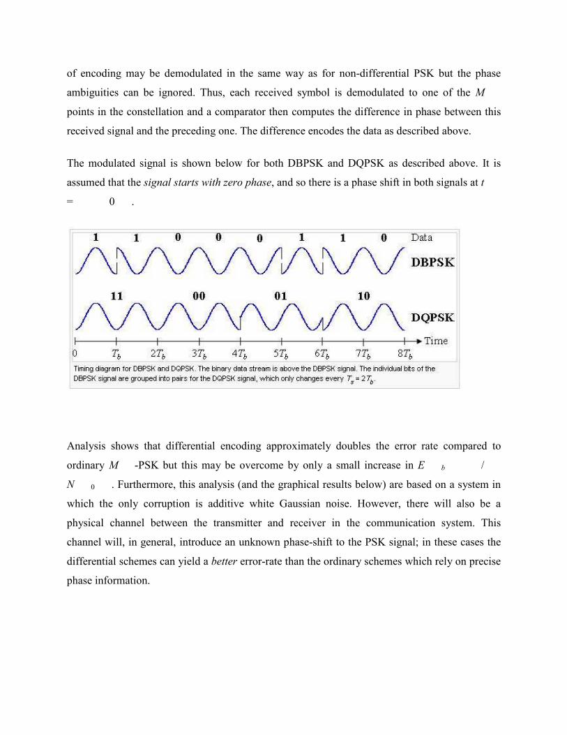
of encoding may be demodulated in the same way as for non-differential PSK but the phase
ambiguities can be ignored. Thus, each received symbol is demodulated to one of the M
points in the constellation and a comparator then computes the difference in phase between this
received signal and the preceding one. The difference encodes the data as described above.
The modulated signal is shown below for both DBPSK and DQPSK as described above. It is
assumed that the signal starts with zero phase, and so there is a phase shift in both signals at t
= 0 .
Analysis shows that differential encoding approximately doubles the error rate compared to
ordinary M -PSK but this may be overcome by only a small increase in E b /
N 0 . Furthermore, this analysis (and the graphical results below) are based on a system in
which the only corruption is additive white Gaussian noise. However, there will also be a
physical channel between the transmitter and receiver in the communication system. This
channel will, in general, introduce an unknown phase-shift to the PSK signal; in these cases the
differential schemes can yield a better error-rate than the ordinary schemes which rely on precise
phase information.
Demodulation
For a signal that has been differentially encoded, there is an obvious alternative method of
demodulation. Instead of demodulating as usual and ignoring carrier-phase ambiguity, the phase
between two successive received symbols is compared and used to determine what the data must
have been. When differential encoding is used in this manner, the scheme is known as
differential phase-shift keying (DPSK). Note that this is subtly different to just differentially-
encoded PSK since, upon reception, the received symbols are not decoded one-by-one to
constellation points but are instead compared directly to one another.
Call the received symbol in the kth
timeslot r k and let it have phase φ k . Assume
without loss of generality that the phase of the carrier wave is zero. Denote the AWGN term as
n k . Then
.
The decision variable for the k − 1th
symbol and the kth
symbol is the phase
difference between r k and r k − 1 . That is, if r k is projected
onto r k − 1 , the decision is taken on the phase of the resultant complex number:
where superscript * denotes complex conjugation. In the absence of noise, the phase of this is
θ k − θ k − 1 , the phase-shift between the two received signals which can be
used to determine the data transmitted.
The probability of error for DPSK is difficult to calculate in general, but, in the case of DBPSK it
is:
which, when numerically evaluated, is only slightly worse than ordinary BPSK, particularly at
higher E b / N 0 values.
Using DPSK avoids the need for possibly complex carrier-recovery schemes to provide an
accurate phase estimate and can be an attractive alternative to ordinary PSK.
In optical communications, the data can be modulated onto the phase of a laser in a differential
way. For the case of BPSK for example, the laser transmits the field unchanged for binary '1',
and with reverse polarity for '0'. In further processing, a photo diode is used to transform the
optical field into an electric current, so the information is changed back into its original state.
The bit-error rates of DBPSK and DQPSK are compared to their non-differential counterparts in
the graph to the right. For DQPSK though, the loss in performance compared to ordinary QPSK
is larger and the system designer must balance this against the reduction in complexity.
1.5 Summary
This section covers the main digital modulation formats, their main applications, relative
spectral efficiencies, and some variations of the main modulation types as used in practical
systems. Fortunately, there are a limited number of modulation types which form the building
blocks of any system.
1.6 Keywords
• Digital information
• Analogue transmission
• modem
• Modulator
• Demodulator
• ASK
• FSK
• BPSK
• QPSK
• QAM
• QAM
• DSSS
• CSS
• FHSS
1.7 Exercise
1. Explain Digital Modulation System.
2. List the Digital Modulation techniques.
3. Explain Phase-shift keying.
Unit 2
Digital Modulation System-2
Structure
1.1 Introduction
1.2 Objectives
1.3. Frequency-shift keying
1.4. Amplitude-shift keying
1.5. Quadrature amplitude modulation
1.6 Summary
1.7 keywords
1.8 Exercise
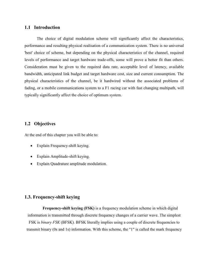
1.1 Introduction
The choice of digital modulation scheme will significantly affect the characteristics,
performance and resulting physical realisation of a communication system. There is no universal
'best' choice of scheme, but depending on the physical characteristics of the channel, required
levels of performance and target hardware trade-offs, some will prove a better fit than others.
Consideration must be given to the required data rate, acceptable level of latency, available
bandwidth, anticipated link budget and target hardware cost, size and current consumption. The
physical characteristics of the channel, be it hardwired without the associated problems of
fading, or a mobile communications system to a F1 racing car with fast changing multipath, will
typically significantly affect the choice of optimum system.
1.2 Objectives
At the end of this chapter you will be able to:
• Explain Frequency-shift keying.
• Explain Amplitude-shift keying.
• Explain Quadrature amplitude modulation.
1.3. Frequency-shift keying
Frequency-shift keying (FSK) is a frequency modulation scheme in which digital
information is transmitted through discrete frequency changes of a carrier wave. The simplest
FSK is binary FSK (BFSK). BFSK literally implies using a couple of discrete frequencies to
transmit binary (0s and 1s) information. With this scheme, the "1" is called the mark frequency
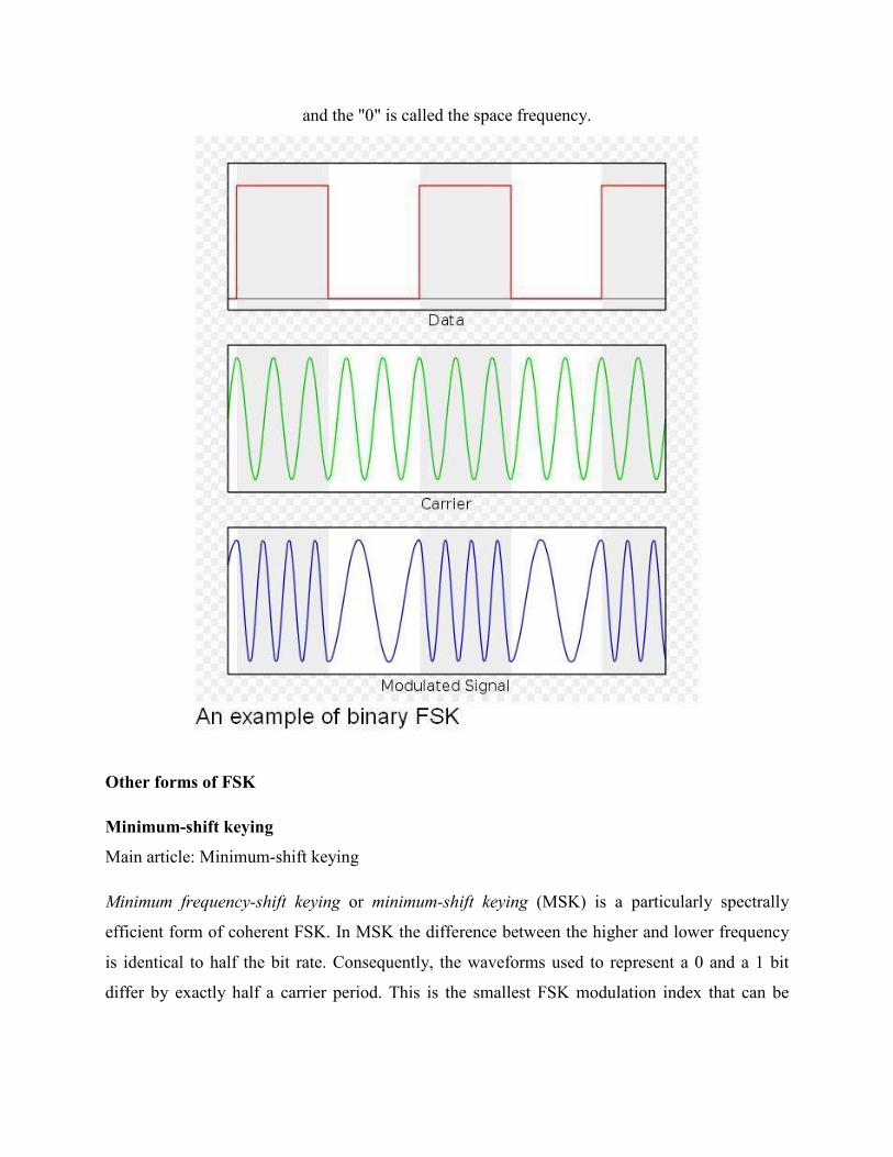
and the "0" is called the space frequency.
Other forms of FSK
Minimum-shift keying
Main article: Minimum-shift keying
Minimum frequency-shift keying or minimum-shift keying (MSK) is a particularly spectrally
efficient form of coherent FSK. In MSK the difference between the higher and lower frequency
is identical to half the bit rate. Consequently, the waveforms used to represent a 0 and a 1 bit
differ by exactly half a carrier period. This is the smallest FSK modulation index that can be
chosen such that the waveforms for 0 and 1 are orthogonal. A variant of MSK called GMSK is
used in the GSM mobile phone standard.
FSK is commonly used in Caller ID and remote metering applications: see FSK standards for use
in Caller ID and remote metering for more details.
Audio FSK
Audio frequency-shift keying (AFSK) is a modulation technique by which digital data is
represented by changes in the frequency (pitch) of an audio tone, yielding an encoded signal
suitable for transmission via radio or telephone. Normally, the transmitted audio alternates
between two tones: one, the "mark", represents a binary one; the other, the "space", represents a
binary zero.
AFSK differs from regular frequency-shift keying in performing the modulation at baseband
frequencies. In radio applications, the AFSK-modulated signal normally is being used to
modulate an RF carrier (using a conventional technique, such as AM or FM) for transmission.
AFSK is not always used for high-speed data communications, since it is far less efficient in both
power and bandwidth than most other modulation modes. In addition to its simplicity, however,
AFSK has the advantage that encoded signals will pass through AC-coupled links, including
most equipment originally designed to carry music or speech.
1.4. Amplitude-shift keying
Amplitude-shift keying (ASK) is a form of modulation that represents digital data as
variations in the amplitude of a carrier wave.
The amplitude of an analog carrier signal varies in accordance with the bit stream (modulating
signal), keeping frequency and phase constant. The level of amplitude can be used to represent
binary logic 0s and 1s. We can think of a carrier signal as an ON or OFF switch. In the
modulated signal, logic 0 is represented by the absence of a carrier, thus giving OFF/ON keying
operation and hence the name given.
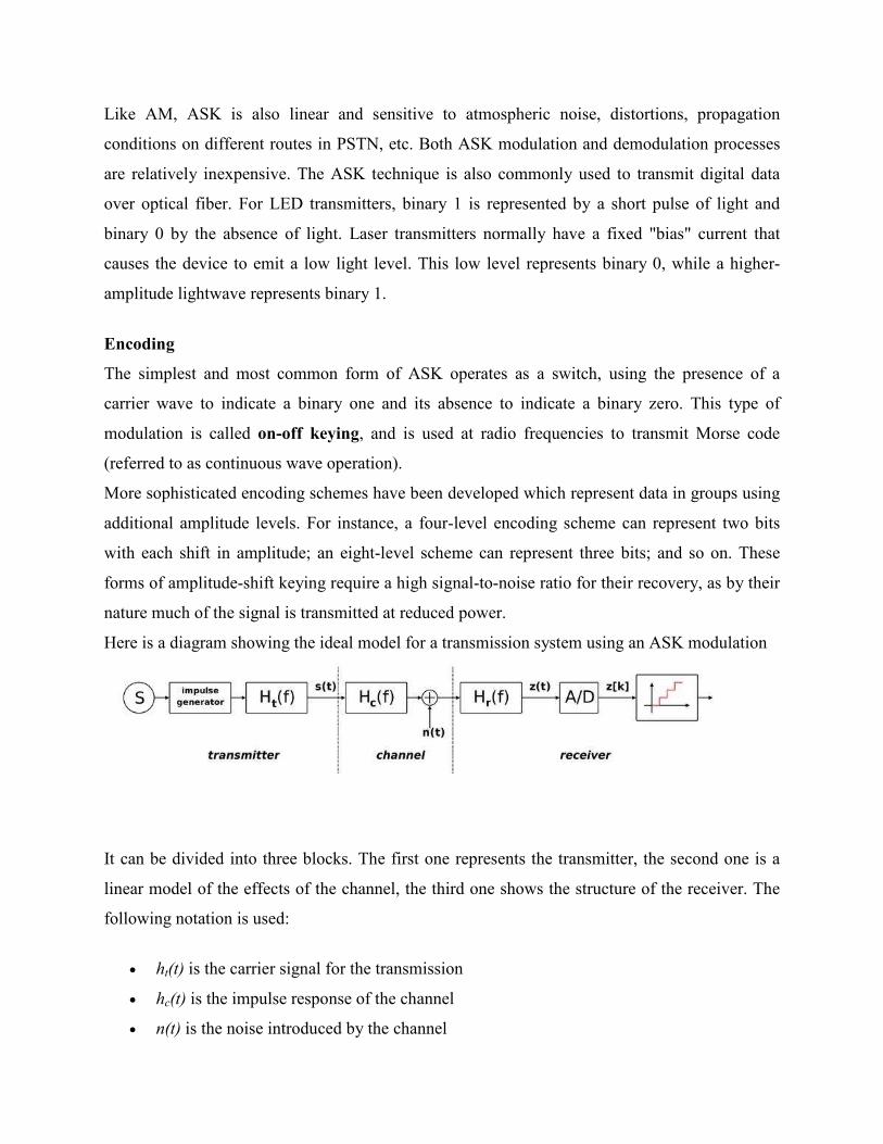
Like AM, ASK is also linear and sensitive to atmospheric noise, distortions, propagation
conditions on different routes in PSTN, etc. Both ASK modulation and demodulation processes
are relatively inexpensive. The ASK technique is also commonly used to transmit digital data
over optical fiber. For LED transmitters, binary 1 is represented by a short pulse of light and
binary 0 by the absence of light. Laser transmitters normally have a fixed "bias" current that
causes the device to emit a low light level. This low level represents binary 0, while a higher-
amplitude lightwave represents binary 1.
Encoding
The simplest and most common form of ASK operates as a switch, using the presence of a
carrier wave to indicate a binary one and its absence to indicate a binary zero. This type of
modulation is called on-off keying, and is used at radio frequencies to transmit Morse code
(referred to as continuous wave operation).
More sophisticated encoding schemes have been developed which represent data in groups using
additional amplitude levels. For instance, a four-level encoding scheme can represent two bits
with each shift in amplitude; an eight-level scheme can represent three bits; and so on. These
forms of amplitude-shift keying require a high signal-to-noise ratio for their recovery, as by their
nature much of the signal is transmitted at reduced power.
Here is a diagram showing the ideal model for a transmission system using an ASK modulation
It can be divided into three blocks. The first one represents the transmitter, the second one is a
linear model of the effects of the channel, the third one shows the structure of the receiver. The
following notation is used:
• ht(t) is the carrier signal for the transmission
• hc(t) is the impulse response of the channel
• n(t) is the noise introduced by the channel
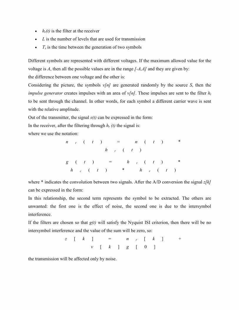
• hr(t) is the filter at the receiver
• L is the number of levels that are used for transmission
• Ts is the time between the generation of two symbols
Different symbols are represented with different voltages. If the maximum allowed value for the
voltage is A, then all the possible values are in the range [-A,A] and they are given by:
the difference between one voltage and the other is:
Considering the picture, the symbols v[n] are generated randomly by the source S, then the
impulse generator creates impulses with an area of v[n]. These impulses are sent to the filter ht
to be sent through the channel. In other words, for each symbol a different carrier wave is sent
with the relative amplitude.
Out of the transmitter, the signal s(t) can be expressed in the form:
In the receiver, after the filtering through hr (t) the signal is:
where we use the notation:
n r ( t ) = n ( t ) *
h r ( t )
g ( t ) = h t ( t ) *
h c ( t ) * h r ( t )
where * indicates the convolution between two signals. After the A/D conversion the signal z[k]
can be expressed in the form:
In this relationship, the second term represents the symbol to be extracted. The others are
unwanted: the first one is the effect of noise, the second one is due to the intersymbol
interference.
If the filters are chosen so that g(t) will satisfy the Nyquist ISI criterion, then there will be no
intersymbol interference and the value of the sum will be zero, so:
z [ k ] = n r [ k ] +
v [ k ] g [ 0 ]
the transmission will be affected only by noise.
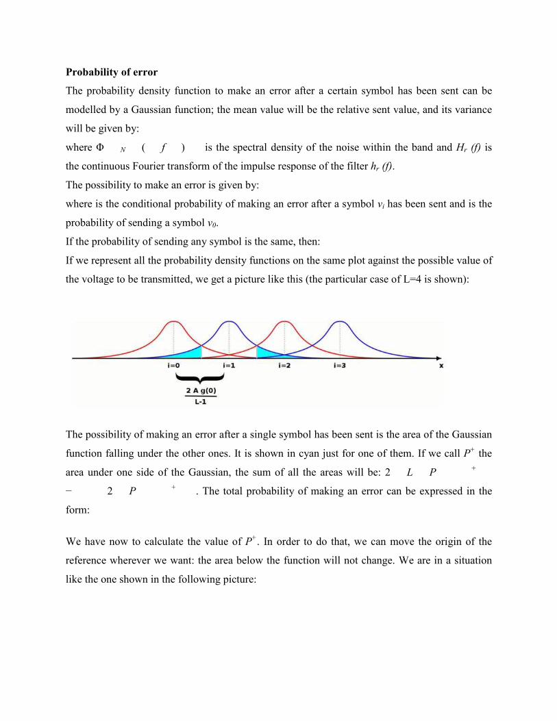
Probability of error
The probability density function to make an error after a certain symbol has been sent can be
modelled by a Gaussian function; the mean value will be the relative sent value, and its variance
will be given by:
where Φ N ( f ) is the spectral density of the noise within the band and Hr (f) is
the continuous Fourier transform of the impulse response of the filter hr (f).
The possibility to make an error is given by:
where is the conditional probability of making an error after a symbol vi has been sent and is the
probability of sending a symbol v0.
If the probability of sending any symbol is the same, then:
If we represent all the probability density functions on the same plot against the possible value of
the voltage to be transmitted, we get a picture like this (the particular case of L=4 is shown):
The possibility of making an error after a single symbol has been sent is the area of the Gaussian
function falling under the other ones. It is shown in cyan just for one of them. If we call P+ the
area under one side of the Gaussian, the sum of all the areas will be: 2 L P +
− 2 P +
. The total probability of making an error can be expressed in the
form:
We have now to calculate the value of P+. In order to do that, we can move the origin of the
reference wherever we want: the area below the function will not change. We are in a situation
like the one shown in the following picture:
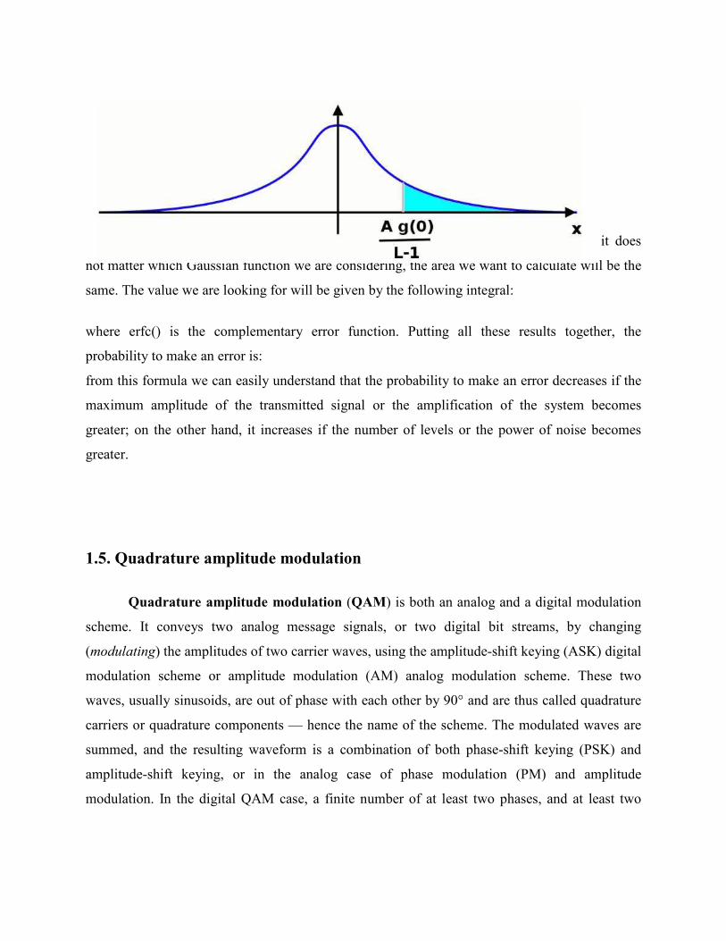
it does
not matter which Gaussian function we are considering, the area we want to calculate will be the
same. The value we are looking for will be given by the following integral:
where erfc() is the complementary error function. Putting all these results together, the
probability to make an error is:
from this formula we can easily understand that the probability to make an error decreases if the
maximum amplitude of the transmitted signal or the amplification of the system becomes
greater; on the other hand, it increases if the number of levels or the power of noise becomes
greater.
1.5. Quadrature amplitude modulation
Quadrature amplitude modulation (QAM) is both an analog and a digital modulation
scheme. It conveys two analog message signals, or two digital bit streams, by changing
(modulating) the amplitudes of two carrier waves, using the amplitude-shift keying (ASK) digital
modulation scheme or amplitude modulation (AM) analog modulation scheme. These two
waves, usually sinusoids, are out of phase with each other by 90° and are thus called quadrature
carriers or quadrature components — hence the name of the scheme. The modulated waves are
summed, and the resulting waveform is a combination of both phase-shift keying (PSK) and
amplitude-shift keying, or in the analog case of phase modulation (PM) and amplitude
modulation. In the digital QAM case, a finite number of at least two phases, and at least two
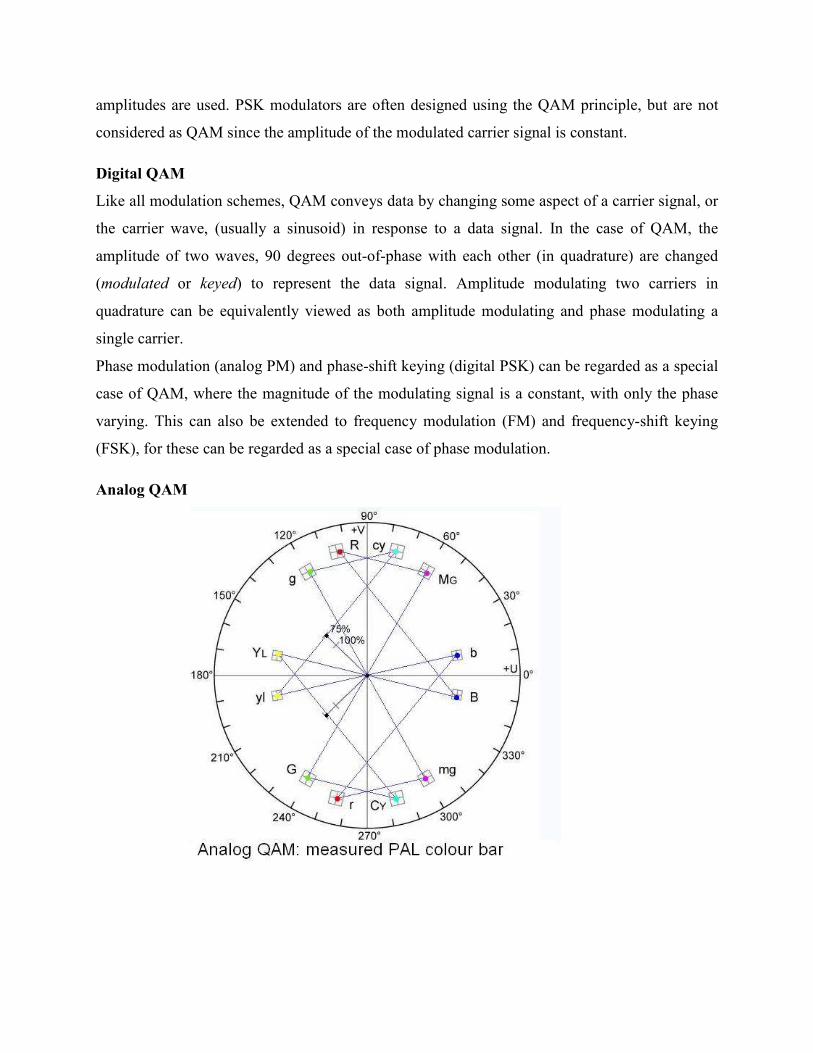
amplitudes are used. PSK modulators are often designed using the QAM principle, but are not
considered as QAM since the amplitude of the modulated carrier signal is constant.
Digital QAM
Like all modulation schemes, QAM conveys data by changing some aspect of a carrier signal, or
the carrier wave, (usually a sinusoid) in response to a data signal. In the case of QAM, the
amplitude of two waves, 90 degrees out-of-phase with each other (in quadrature) are changed
(modulated or keyed) to represent the data signal. Amplitude modulating two carriers in
quadrature can be equivalently viewed as both amplitude modulating and phase modulating a
single carrier.
Phase modulation (analog PM) and phase-shift keying (digital PSK) can be regarded as a special
case of QAM, where the magnitude of the modulating signal is a constant, with only the phase
varying. This can also be extended to frequency modulation (FM) and frequency-shift keying
(FSK), for these can be regarded as a special case of phase modulation.
Analog QAM
When transmitting two signals by modulating them with QAM, the transmitted signal will be of
the form:
where I ( t ) and Q ( t ) are the modulating signals and f 0 is the
carrier frequency.
At the receiver, these two modulating signals can be demodulated using a coherent demodulator.
Such a receiver multiplies the received signal separately with both a cosine and sine signal to
produce the received estimates of I ( t ) and Q ( t ) respectively.
Because of the orthogonality property of the carrier signals, it is possible to detect the
modulating signals independently.
In the ideal case I ( t ) is demodulated by multiplying the transmitted signal with a
cosine signal:
Using standard trigonometric identities, we can write it as:
Low-pass filtering r i ( t ) removes the high frequency terms (containing
4 π f 0 t ), leaving only the I ( t ) term. This filtered signal is
unaffected by Q ( t ) , showing that the in-phase component can be received
independently of the quadrature component. Similarly, we may multiply s ( t ) by a
sine wave and then low-pass filter to extract Q ( t ) .
The phase of the received signal is assumed to be known accurately at the receiver. This issue of
carrier synchronization at the receiver must be handled somehow in QAM systems. The coherent
demodulator needs to be exactly in phase with the received signal, or otherwise the modulated
signals cannot be independently received. For example analog television systems transmit a burst
of the transmitting colour subcarrier after each horizontal synchronization pulse for reference.
Analog QAM is used in NTSC and PAL television systems, where the I- and Q-signals carry the
components of chroma (colour) information. "Compatible QAM" or C-QUAM is used in AM
stereo radio to carry the stereo difference information.
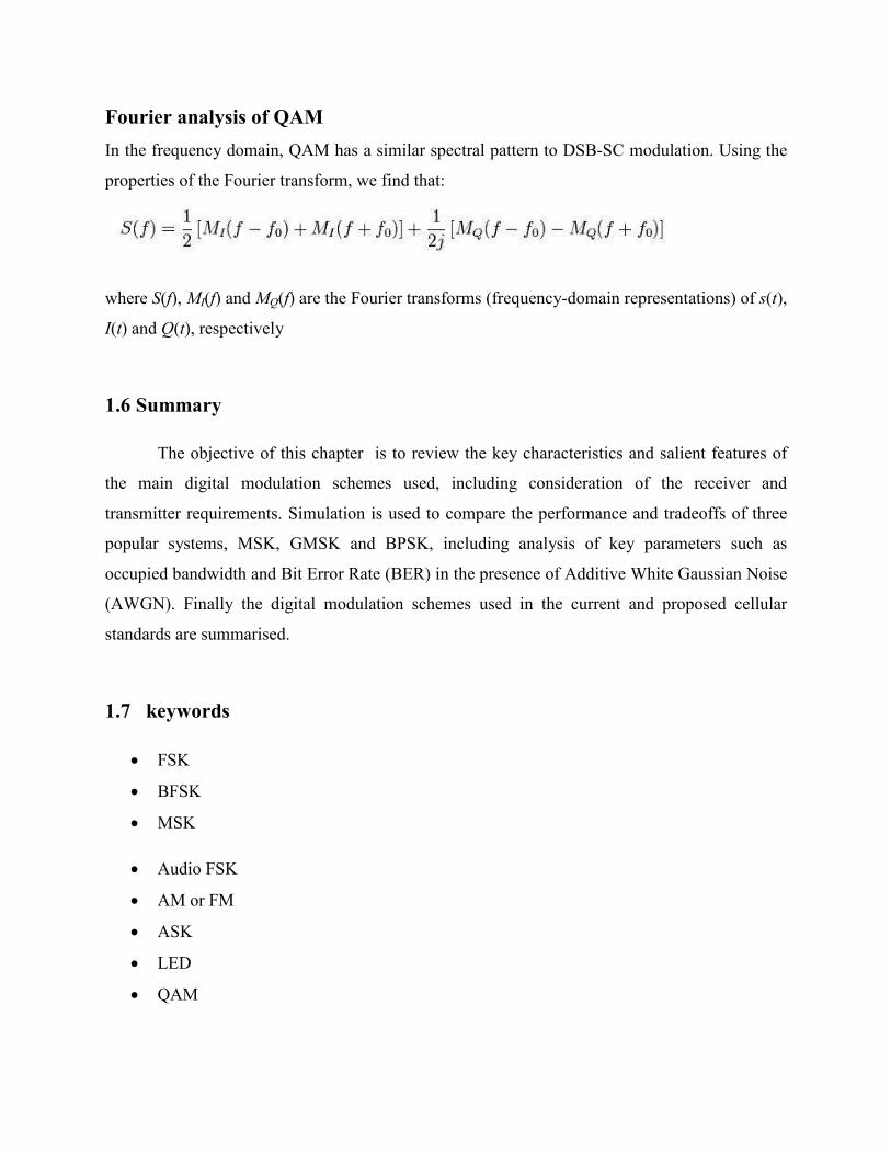
Fourier analysis of QAM
In the frequency domain, QAM has a similar spectral pattern to DSB-SC modulation. Using the
properties of the Fourier transform, we find that:
where S(f), MI(f) and MQ(f) are the Fourier transforms (frequency-domain representations) of s(t),
I(t) and Q(t), respectively
1.6 Summary
The objective of this chapter is to review the key characteristics and salient features of
the main digital modulation schemes used, including consideration of the receiver and
transmitter requirements. Simulation is used to compare the performance and tradeoffs of three
popular systems, MSK, GMSK and BPSK, including analysis of key parameters such as
occupied bandwidth and Bit Error Rate (BER) in the presence of Additive White Gaussian Noise
(AWGN). Finally the digital modulation schemes used in the current and proposed cellular
standards are summarised.
1.7 keywords
• FSK
• BFSK
• MSK
• Audio FSK
• AM or FM
• ASK
• LED
• QAM
• Fourier analysis of QAM
1.8 Exercise
1. Explain Frequency-shift keying.
2. Explain Amplitude-shift keying.
3. Explain Quadrature amplitude modulation.
Unit 3
Communication Over band limited channels
Structure
3.1 Introduction
3.2 Objectives
3.3 Bandlimited channels
3.4 Digital Signaling Through Bandlimited Awgn Channels
3.5 Equalization Techniques
3.6 Further Discussion
3.7 Summary
3.8 Keywords
3.9 Exercise
3.1 Introduction
Thus far in this course, we have been treating the communication channel as having no
effect on the signal, or at worst simply as attenuating the transmitted signal by some known
factor. Thus, the energy E that has been the subject of much discussion could be referred to as
the received energy (which is what it is) or as the transmitted energy since the two quantities
were identical, or at worst, had a known linear relationship. If we were to model such a channel
as a linear time-invariant system with impulse response g(t), then g(t) would be taken to be δ(t)
where δ(t) denotes the unit impulse.
Thus, the channel output would be the same as the input, or the input attenuated by a
factor α . In practice, all channels change the transmitted signal in ways other than simple
attenuation, but when the channel has bandwidth much larger than that of the transmitted signal,
and G(f) is essentially a constant over the frequency band of interest, then it is a reasonable
approximation to model g(t) as δ(t) or α*δ(t). Otherwise, when the channel transfer function
varies significantly over the frequency band of interest, the e effect of the channel on the
transmitted signal needs to be taken into account. Such channels are called band-limited or
bandwidth-limited channels and they cause a phenomenon called inter symbol interference. As
the name implies, inter symbol interference (ISI) means that each sample value in the receiver
depends not just on the symbol being demodulated but also on other symbols being transmitted.
The presence of these extraneous symbols interferes with the demodulation process. For
example, the designs for optimum receivers for signals received over AWGN channels that we
have been studying thus far do not take ISI into account at all, and when ISI is present, their
performance can be quite poor. In this Lecture and the next few, we shall study how ISI arises,
and how to to mitigate its effects on the performance of communication systems operating over
band-limited channels.
3.2 Objectives
At the end of this chapter you will be able to:
• Explain Band limited channels.
• Know Digital Signaling Through Bandlimited Awgn Channels.
• Give Equalization Techniques.
3.3 Bandlimited channels
Another cause of intersymbol interference is the transmission of a signal through
a bandlimited channel, i.e., one where the frequency response is zero above a certain frequency
(the cutoff frequency). Passing a signal through such a channel results in the removal of
frequency components above this cutoff frequency; in addition, the amplitude of the frequency
components below the cutoff frequency may also be attenuated by the channel.
This filtering of the transmitted signal affects the shape of the pulse that arrives at the receiver.
The effects of filtering a rectangular pulse; not only change the shape of the pulse within the first
symbol period, but it is also spread out over the subsequent symbol periods. When a message is
transmitted through such a channel, the spread pulse of each individual symbol will interfere
with following symbols.
As opposed to multipath propagation, bandlimited channels are present in both wired and
wireless communications. The limitation is often imposed by the desire to operate multiple
independent signals through the same area/cable; due to this, each system is typically allocated a
piece of the total bandwidth available. For wireless systems, they may be allocated a slice of
the electromagnetic spectrum to transmit in (for example, FM radio is often broadcast in the
87.5 MHz - 108 MHz range). This allocation is usually administered by a government agency; in
the case of the United Statesthis is the Federal Communications Commission (FCC). In a wired
system, such as an optical fiber cable, the allocation will be decided by the owner of the cable.
The bandlimiting can also be due to the physical properties of the medium - for instance, the
cable being used in a wired system may have a cutoff frequency above which practically none of
the transmitted signal will propagate.
Communication systems that transmit data over bandlimited channels usually implement pulse
shaping to avoid interference caused by the bandwidth limitation. If the channel frequency
response is flat and the shaping filter has a finite bandwidth, it is possible to communicate with
no ISI at all. Often the channel response is not known beforehand, and an adaptive equalizer is
used to compensate the frequency response.
3.4 Optimum Pulse Shape Design for Digital Signaling Through
Bandlimited Awgn Channels
We treat digital communication over a channel that is modeled as a linear filter with a
bandwidth limitation. The bandwidth constrain generally precludes the use of rectangular pulses
at the output of the modulator. Instead, the transmitted signals must be shaped to restrict their
bandwidth to that available on the channel. The channel distortion results in intersymbol
interference (ISI) at the output of the demodulator and leads to an increase in the probability of
error at the detector. Devices or methods for correcting or undoing the channel distortion, called
channel equalizers.
A bandlimited channel is characterized as a linear filter with impulse response c(t) and frequency
response c(f),
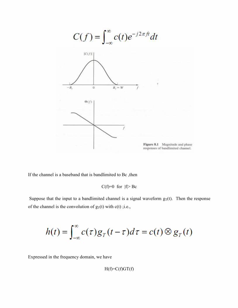
If the channel is a baseband that is bandlimited to Bc ,then
Suppose that the input to a bandlimited channel is a signal waveform g
of the channel is the convolution of g
Expressed in the frequency domain, we have
If the channel is a baseband that is bandlimited to Bc ,then
C(f)=0 for |f|> Bc
Suppose that the input to a bandlimited channel is a signal waveform gT(t). Then the response
of the channel is the convolution of gT(t) with c(t) ;i.e.,
Expressed in the frequency domain, we have
H(f)=C(f)GT(f)
(t). Then the response
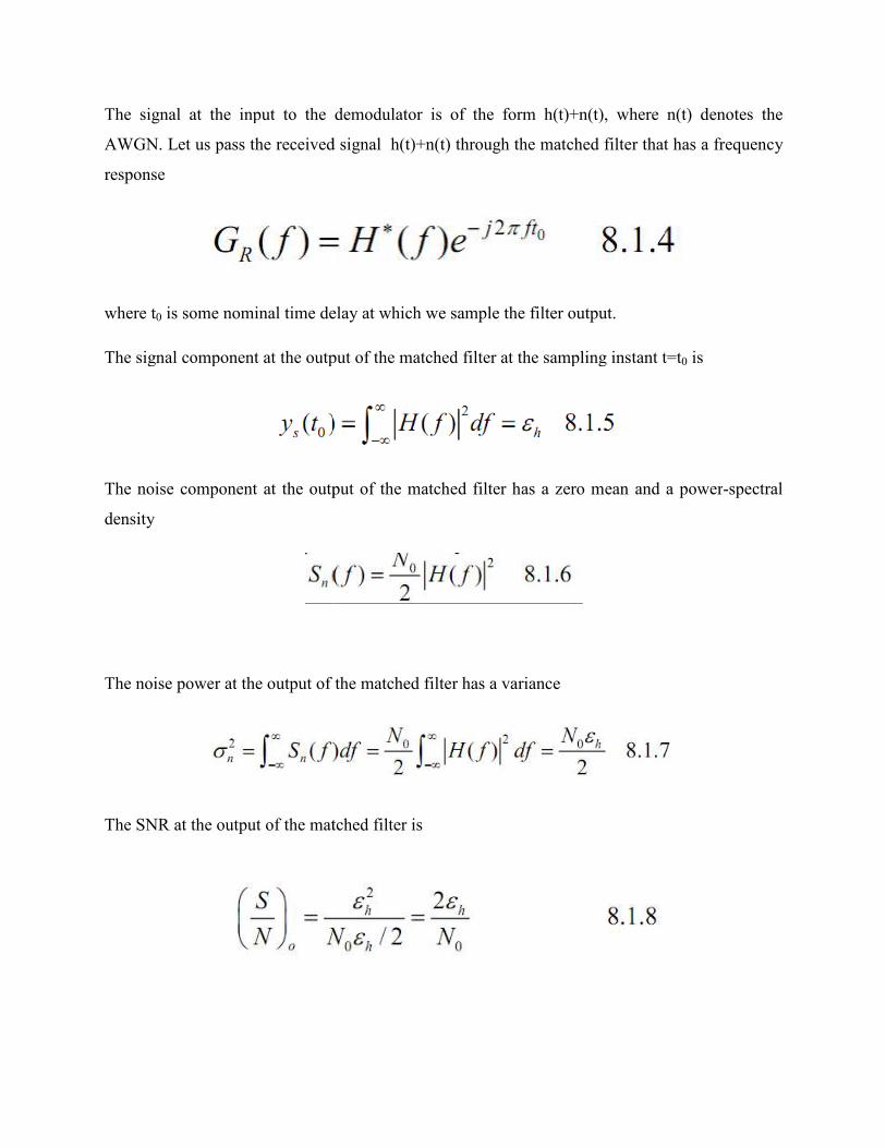
The signal at the input to the demodulator is of the form h(t)+n(t), where n(t) denotes the
AWGN. Let us pass the received signal h(t)+n(t) through the matched filter that has a frequency
response
where t0 is some nominal time delay at which we sample the filter output.
The signal component at the output of the matched filter at the sampling instant t=t
The noise component at the output of the matched filter has a zero mean and a power
density
The noise power at the output of the matched filter has a
The SNR at the output of the matched filter is
input to the demodulator is of the form h(t)+n(t), where n(t) denotes the
AWGN. Let us pass the received signal h(t)+n(t) through the matched filter that has a frequency
is some nominal time delay at which we sample the filter output.
The signal component at the output of the matched filter at the sampling instant t=t
The noise component at the output of the matched filter has a zero mean and a power
The noise power at the output of the matched filter has a variance
The SNR at the output of the matched filter is
input to the demodulator is of the form h(t)+n(t), where n(t) denotes the
AWGN. Let us pass the received signal h(t)+n(t) through the matched filter that has a frequency
The signal component at the output of the matched filter at the sampling instant t=t0 is
The noise component at the output of the matched filter has a zero mean and a power-spectral
Compared to the previous result, the major difference in this development is that the filter
impulse response is matched to the received signal h(t) instead of the transmitted signal.
3.5 Equalization Techniques
Due to the distortive character of the propagation environment, transmitted data symbols
will spread out in time and will interfere with each other, a phenomenon called Inter Symbol
Interference (ISI). The degree of ISI depends on the data rate: the higher the data rate, the more
ISI is introduced. On the other hand, changes in the propagation environment, e.g., due to
mobility in wireless communications, introduce channel time-variation, which could be very
harmful.
Mitigating these fading channel effects, also referred to as channel equalization,
constitutes a major challenge in current and future communication systems. In order to design a
good channel equalizer, a practical channel model has to be derived. First of all, we can write the
overall system as a symbol rate Single-Input Multiple-Output (SIMO) system, where the
multiple outputs are obtained by multiple receive antennas and/or fractional sampling. Then,
looking at a fixed time-window, we can distinguish between Time-InVariant (TIV) and Time-
Varying (TV) channels. For TIV channels, we will model the channel by a TIV FIR channel,
whereas for TV channels, it will be convenient to model the channel time-variation by means of
a Basis Expansion Model (BEM), leading to a BEM FIR channel [40], [14], [33]. For TIV
channels, channel equalizers have been extensively studied in literature (see for instance [30, ch.
10], [19, ch. 10], [15, ch. 5], [12] and references therein). For TV channels, on the other hand,
they have only been introduced recently. Instead of focusing on complex Maximum Likelihood
(ML) or Maximum A Posteriori (MAP) equalizers, we will discuss more practical finite-length
linear and decision feedback equalizers. We derive Minimum Mean-Square Error (MMSE)
solutions, which strike an optimal balance between ISI removal and noise enhancement.
By setting the signal power to infinity, these MMSE solutions can easily be transformed into
Zero-Forcing (ZF) solutions that completely remove the ISI. We mainly focus on equalizer
design based on channel knowledge, and briefly mention channel estimation algorithms and
direct equalizer design algorithms, which do not require channel knowledge.
3.6 Further Discussion
Further Abstract-Continuous-time additive white Gaussian noise channels with strictly
time-limited and root-mean-square (RMS) bandlimited inputs are studied. RMS bandwidth is
equal to the normalized second moment of the spectrum, which has proved to be a useful and
analytically tractable measure of the bandwidth of strictly time-limited waveforms. The capacity
of the single-user and two-user RMS-bandlimited channels are found in easy-to-compute
parametric forms, and are compared to the classical formulas for the capacity of strictly
bandlimited channels. In addition, channels are considered where the inputs are further
constrained to be pulse amplitude modulated (PAM) waveforms. The capacity of the single-user
RMS-bandlimited PAM channel is shown to coincide with Shannon’s capacity formula for the
strictly bandlimited channel. This shows that the laxer bandwidth constraint precisely offsets the
PAM structural constraint, and illustrates a tradeoff between the time domain and frequency
domain constraints. In the synchronous two-user channel, we find the pair of pulses that achieves
the boundary of the capacity region, and show that the shapes of the optimal pulses depend not
only on the bandwidth but also on the respective signal-to-noise ratios. Index Terms-Bandlimited
communication, information rate, multiuser channels.
3.7 Summary
The designs for optimum receivers for signals received over AWGN channels that we
have been studying thus far do not take ISI into account at all, and when ISI is present, their
performance can be quite poor. In this Lecture and the next few, we shall study how ISI arises,
and how to to mitigate its effects on the performance of communication systems operating over
band-limited channels.
Communication systems that transmit data over bandlimited channels usually implement pulse
shaping to avoid interference caused by the bandwidth limitation. If the channel frequency
response is flat and the shaping filter has a finite bandwidth, it is possible to communicate with
no ISI at all. Often the channel response is not known beforehand, and an adaptive equalizer is
used to compensate the frequency response.
3.8 Keywords
• ISI
• MHz
• SIMO
• TIV
• BEM
• MMSE
• ZF
• RMS
• PAM
3.9 Exercise
1. Explain Band limited channels.
2. Explain Digital Signaling Through Bandlimited Awgn Channels.
3. Give Equalization Techniques.


