Embed Size (px)
Citation preview

Copyright 2001, Agrawal & Bushnell
VLSI Test: Lecture 19 1
Lecture 19Fault-Model Based
Structural Analog Testing
Lecture 19Fault-Model Based
Structural Analog Testing
Analog fault models Analog Fault Simulation
DC fault simulation AC fault simulation
Analog Automatic Test-Pattern Generation
Using Sensitivities Using Signal Flow Graphs
Summary

Copyright 2001, Agrawal & Bushnell
VLSI Test: Lecture 19 2
Types of Structural Faults
Types of Structural Faults
Catastrophic (hard): Component is completely open or
completely shorted Easy to test for
Parametric (soft):
Analog R, C, L, Kn, or Kp (a transistor K
parameter) is outside of its tolerance box)
Very hard to test for

Copyright 2001, Agrawal & Bushnell
VLSI Test: Lecture 19 3
Analog Fault ModelsAnalog Fault Models
First stage gain R2 / R1
High-pass filter gain R3 and C1
High-pass filter cutoff f C1
Low-pass AC voltage gain R4, R5, & C2
Low-pass DC voltage gain R4 and R5
Low-pass filter cutoff f C2

Copyright 2001, Agrawal & Bushnell
VLSI Test: Lecture 19 4
Levels of AbstractionLevels of Abstraction
Structural Level
Structural View – Transistor schematic
Behavioral View – System of non-linear partial differential equations for netlist
Functional Level
Structural View – Signal Flow Graph
Behavioral View – Analog network transfer function

Copyright 2001, Agrawal & Bushnell
VLSI Test: Lecture 19 5
Analog Test TypesAnalog Test Types
Specification Tests
Design characterization – Does design meet specifications?
Diagnostic – Find cause of failures
Production tests – Test large numbers of linear/mixed-signal circuits

Copyright 2001, Agrawal & Bushnell
VLSI Test: Lecture 19 6
DC Analog Fault Simulation
DC Analog Fault Simulation

Copyright 2001, Agrawal & Bushnell
VLSI Test: Lecture 19 7
Complementarity PivotingComplementarity Pivoting P. M.Lin and Y. S. Elcherif, Analogue Circuits Fault
Dictionary – New Approaches and Implementation, Int’l. J. of Circuit Theory and Applications, 1985
Model all non-linear devices with piecewise-linear I-V characteristics (ideal diodes)
Represent open, short, and parametric faults with switches
Formulate as n-port network complementarity problem
Solve with Lemke’s complementarity pivoting algorithm Use m pairs of complementarity variables
(port currents and voltages)

Copyright 2001, Agrawal & Bushnell
VLSI Test: Lecture 19 8
One-Step RelaxationOne-Step Relaxation
W. Tian and C.-J. Shi, Nonlinear DC-Fault Simulation by One-Step Relaxation – Linear Circuit Models are Sufficient for Nonlinear DC–Fault Simulation, VTS-1998
Solve f (x) = 0, x is circuit variable vector (node voltages and branch currents), f is non-linear system function
Guess x (0)
Solve Jacobian: Jf (xg) (xf(1) – xg)= -ff (xg)
Operate Newton-Raphson algorithm for only 1 step

Copyright 2001, Agrawal & Bushnell
VLSI Test: Lecture 19 9
Fault OrderingFault OrderingW. Tian and C.-J. Shi, Efficient DC Fault Simulation of
Nonlinear Analog Circuits, DATE-98

Copyright 2001, Agrawal & Bushnell
VLSI Test: Lecture 19 10
AC Fault SimulationAC Fault Simulation

Copyright 2001, Agrawal & Bushnell
VLSI Test: Lecture 19 11
Householder’s FormulaHouseholder’s Formula A. S. Householder, A Survey of Some Closed
Methods for Inverting Matrices, SIAM J. of Applied Mathematics, 1957
Analyze circuit with Modified Nodal Analysis:
T x = w Equivalent faulty circuit equation:
Tf xf = wf
Formula (Tf differs only a little from T):
(A + U S W)-1 = A-1 – A-1 U (S-1 + WA-1 U)-1 W A-1
Reduces amount of equation solving – 10 x speedup over sparse matrix techniques

Copyright 2001, Agrawal & Bushnell
VLSI Test: Lecture 19 12
Discrete Z-Domain Mapping
Discrete Z-Domain Mapping
Nagi, Chatterjee, Abraham, DRAFTS: Discretized Analog Circuit Fault Simulator, Design Automation Conference, 1993
Analog circuit fault simulation with Signal Flow Graph (SFG)
Represented complex frequency state equations using SFGs and dummy variables
Use bilinear transform, map s-domain equations into z-domain
Accelerated fault simulation 10 times with behavioral OPAMP models

Copyright 2001, Agrawal & Bushnell
VLSI Test: Lecture 19 13
Monte-Carlo SimulationMonte-Carlo Simulation
Perform analog simulation for randomly-generated small variations in analog circuit component values
Actual IC manufacturing makes good circuits deviate by such values
Good in practice but good and bad machines have different worst-case corners Tends to underestimate circuit
response bounds – may claim faults are detectable when they are not

Copyright 2001, Agrawal & Bushnell
VLSI Test: Lecture 19 14
Analog Automatic Test-Pattern Generation
Analog Automatic Test-Pattern Generation

Copyright 2001, Agrawal & Bushnell
VLSI Test: Lecture 19 15
Method of ATPG Using Sensitivities
Method of ATPG Using Sensitivities
Compute analog circuit sensitivities Construct analog circuit bipartite graph From graph, find which O/P parameters
(performances) to measure to guarantee maximal coverage of parametric faults Determine which O/P parameters are
most sensitive to faults Evaluate test quality, add test points to
complete the analog fault coverage
N. B. Hamida and B. Kaminska, Analog Circuit Testing Based on Sensitivity Computation and New Circuit Modeling, ITC-1993

Copyright 2001, Agrawal & Bushnell
VLSI Test: Lecture 19 16
SensitivitySensitivity Differential:
S =
Incremental:
= x
Tj – performance parameter
xi – network element
Tj
xi
xi Tj
Tj xi
Tj / Tj
xi / xi xi 0
Tj
xi
xi
Tj
Tj
xi

Copyright 2001, Agrawal & Bushnell
VLSI Test: Lecture 19 17
Circuit ModelCircuit Model

Copyright 2001, Agrawal & Bushnell
VLSI Test: Lecture 19 18
Incremental Sensitivity Matrix of Circuit
Incremental Sensitivity Matrix of Circuit
-0.9100000
R1
100000
R2
00.58-0.91
000
C1
00.38-0.89
000
R3
000
-0.96-0.97
0
R4
000
0.48-0.97-0.88
R5
000
-0.480
-0.91
C2
A1
A2
fc1
A3
A4
fc2
\

Copyright 2001, Agrawal & Bushnell
VLSI Test: Lecture 19 19
Bipartite Graph of CircuitBipartite Graph of Circuit

Copyright 2001, Agrawal & Bushnell
VLSI Test: Lecture 19 20
Single Fault Best and Worst-Case DeviationsSingle Fault Best and
Worst-Case Deviations
A1
A2
A4
5 15.98
5 14.1
5 20.27
5 11.6
5 15
5 15
R1
R1
R2
R2
R3
R3
C1
C1
R4
R4
R5
R5
fc1
fc2
A3
5 14.81
5 15.2
5 14.65
5 13.96
5 15
5 35
5 35
R3
R3
C1
C1
R5
R5
C2
C2
R4
R4
R5
R5
C2
C2
{ {
{ { { {

Copyright 2001, Agrawal & Bushnell
VLSI Test: Lecture 19 21
Weighted Bipartite GraphWeighted Bipartite Graph
Copyright 2001, Agrawal & Bushnell
VLSI Test: Lecture 19 22
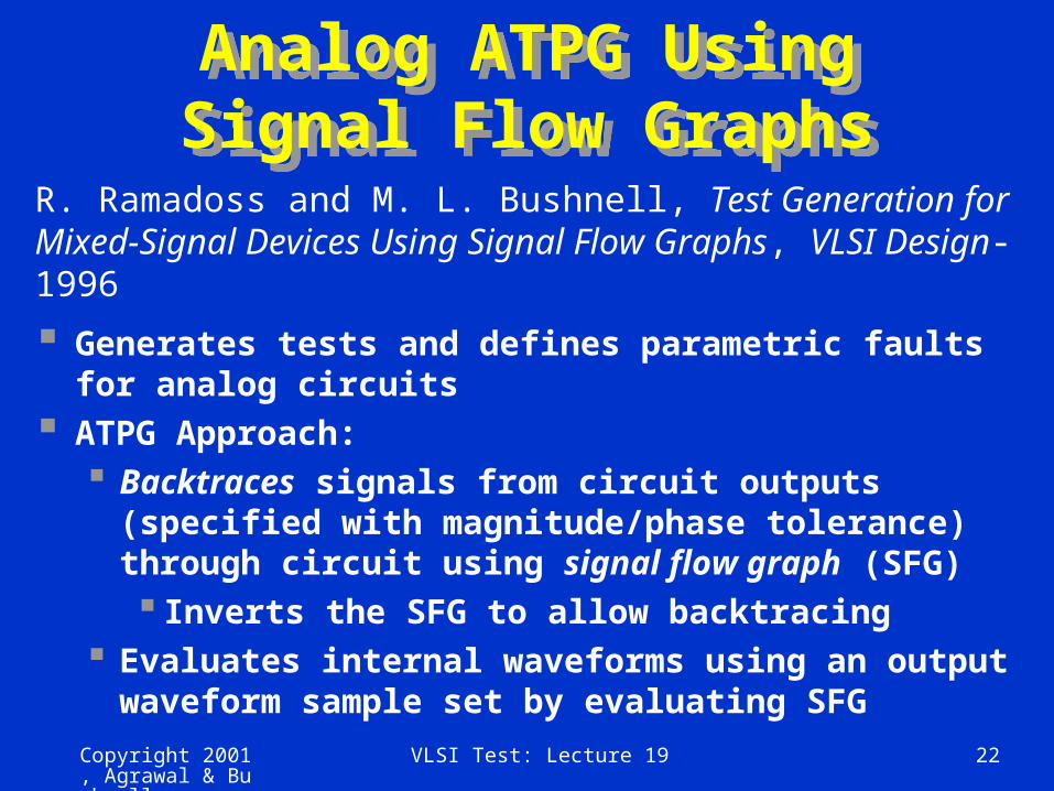
Generates tests and defines parametric faults for analog circuits
ATPG Approach: Backtraces signals from circuit outputs
(specified with magnitude/phase tolerance) through circuit using signal flow graph (SFG) Inverts the SFG to allow backtracing
Evaluates internal waveforms using an output waveform sample set by evaluating SFG
Analog ATPG Using Signal Flow GraphsAnalog ATPG Using Signal Flow Graphs
R. Ramadoss and M. L. Bushnell, Test Generation for Mixed-Signal Devices Using Signal Flow Graphs, VLSI Design-1996

Copyright 2001, Agrawal & Bushnell
VLSI Test: Lecture 19 23
Test Generation via Reverse SimulationTest Generation via Reverse Simulation
Find good circuit signal values at all nodes using good output waveform
Find bad circuit signal values at all nodes using bad output waveform (use extrema of tolerance box for magnitude or phase)
Finds faulty value of analog component necessary to drive output waveform out of tolerance box Mark all corresponding edges to fault Compute modified SFG weights that give
good value after bad edges in inverted SFG

Copyright 2001, Agrawal & Bushnell
VLSI Test: Lecture 19 24
Integrator ExampleIntegrator Example
Basic integrator circuit with ideal OPAMP

Copyright 2001, Agrawal & Bushnell
VLSI Test: Lecture 19 25
Signal Flow Graph Inversion
Signal Flow Graph Inversion
SFG represents analog network equations value (i) = (parent node value) (edge weight) May be inverted
x2 = ax1 + bx3 + cx4 x1 = 1/a x2 – b/a x3 - c/a x4
ORIGINAL GRAPH INVERTED GRAPH SFG inversion algorithm follows from Balabanian’s
example (1969)
Copyright 2001, Agrawal & Bushnell
VLSI Test: Lecture 19 26
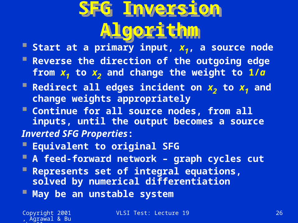
SFG Inversion Algorithm
SFG Inversion Algorithm
Start at a primary input, x1, a source node Reverse the direction of the outgoing edge
from x1 to x2 and change the weight to 1/a
Redirect all edges incident on x2 to x1 and change weights appropriately
Continue for all source nodes, from all inputs, until the output becomes a source
Inverted SFG Properties: Equivalent to original SFG A feed-forward network – graph cycles cut Represents set of integral equations,
solved by numerical differentiation May be an unstable system

Copyright 2001, Agrawal & Bushnell
VLSI Test: Lecture 19 27
Graphs for IntegratorGraphs for Integrator
Original SFG Inverted SFG
SFG part after fault has faulty value Bad signal does not disappear, circuits are
linear Method applicable to all circuits representable
with SFGs (1st and 2nd order) Backtrace over all paths from outputs to inputs 2nd order approximation for s differential
operator

Copyright 2001, Agrawal & Bushnell
VLSI Test: Lecture 19 28
Analog Fault DefinitionAnalog Fault Definition
Want to find parametric fault value for R1 Use good & bad node values for all nodes
from reverse analog simulation For parametric fault definition in inverted
SFG Use good values for nodes before fault Use bad values for nodes after fault Linear equation in 1 variable for each
component Manipulate component equations
symbolically to get component tolerance

Copyright 2001, Agrawal & Bushnell
VLSI Test: Lecture 19 29
Calculation of R1 Tolerance to Cause Fault
Calculation of R1 Tolerance to Cause Fault
goodval (1) badval (3) -R1 C -Rf C
badval (R1) - goodval (1)
C (badval (2) + badval (3) / Rf C)
goodval (R1) - goodval (1)
C (goodval (2) + goodval (3) / Rf C)
R1 Tolerance = goodval (R1) – badval (R1)
+ = badval (2)
=
=
Inverted SFGOriginal SFG

Copyright 2001, Agrawal & Bushnell
VLSI Test: Lecture 19 30
SFG ATPG ResultsSFG ATPG Results
R1 = 10 K, Rf = 100 K, C = 0.01 F
Output tolerance = +10%, used SPICE output
Calculated test signal and component deviations
Deviations analogous to fault coverage
Component
R1
Rf
C
Allowed Value9.09 K80.99 K0.0093 F
Deviation-9.1%
-19.01%-7.0%

Copyright 2001, Agrawal & Bushnell
VLSI Test: Lecture 19 31
Generated Test WaveformGenerated Test WaveformV
olt
ag
e
Time (ms)

Copyright 2001, Agrawal & Bushnell
VLSI Test: Lecture 19 32
Summary of SFG Method
Summary of SFG Method
Works for multiple input, multiple output circuits
Handles single and multiple parametric faults, and catastrophic faults Symbolic solution too difficult for
multiple parametric fault tolerance – use iterative method with simulation to obtain deviation
Extended to cover transistor biasing faults in analog circuits
Extended to analog multipliers and comparators

Copyright 2001, Agrawal & Bushnell
VLSI Test: Lecture 19 33
SummarySummary Analog model-based testing – Just
starting to get some acceptance
Structural test with a fault model
Offers advantage of testing specific parametric and catastrophic faults
Analog DSP-based testing – Main stream
Functional test without fault model
Problem is worsening – 22-bit A/D converters coming, expected to sample at 1 GHz