Embed Size (px)
Citation preview
103
CHAPTER 4
PARAMETRIC OPTIMIZATION OF SYMMETRIC TOGGLE SWITCH
In this chapter, parametric optimization and development of high-k dielectric based
STS has been presented. As discussed in Chapter 3, the electrical characteristics of a
capacitive switch, (isolation, return loss and insertion loss) depend on the (Cdown/Cup) ratio,
which in turn is a function of technology depended parameters such as the gap between the
movable membrane and transmission line (g0), the thickness of dielectric layer (td) and the
dielectric constant (εr) of the material over the transmission line [1]. Cdown and Cup are given
by Eqn. 3.59 and Eqn. 3.60. As described by Eqn. 3.61, (εr/td) ratio can be optimized to
achieve 10-15 times higher capacitance ratio as compared to increase in gap variation (g0).
Raising the gap height (g0), increases the additional processing complexity. Also, lowering
the dielectric thickness below 100 nm causes the dielectric breakdown at lower voltage.
Thus, in order to achieve better RF performance and compact device size, a dielectric with
high dielectric constant is desirable. Silicon dioxide (εr = 3.9) and silicon nitride (εr = 7.9)
are the commonly used dielectric materials for MEMS switches. However, poor resistance
to dielectric charging and charge trapping in the Si3N4 leads to stiction in MEMS capacitive
switches. Also, it is difficult to deposit pin hole free Si3N4 layers below 100 nm. SiO2
provides defect free layers and has a good process compatibility. However, low dielectric
constant of SiO2 results in low capacitance ratio for given dimensions. As discussed in
chapter 3, STS has been designed and fabricated with SiO2 dielectric layer. The measured
results are quite promising as significantly high capacitance ratio with high isolation in off-
state and high return loss in on-state has been attained. The dimensions of SiO2 based STS
are quite large, increasing the inbuilt stress related deformation and reliability issues as
compared to the other existing RF MEMS switches. Using a high-k dielectric material not
only helps in enhancing the electrical properties of the switch, but also enhances the
mechanical properties with small overall dimensions.
High-k dielectrics have been reported as good candidate materials for capacitive
MEMS switches but with few related experimental studies. The materials that could
potentially replace SiO2 and Si3N4 are tantalum oxide (εr = 25), hafnium oxide (19 - 25),
104
barium strontium titanate oxide (28), and strontium titanate oxide (30 - 120), etc. Many of
these materials are thermodynamically unstable on silicon or lack in other desirable
properties such as high dielectric breakdown voltage, resistance to dielectric charging, low
defect density, good adhesion, thermal stability, low deposition temperature and the ability
to pattern. Hafnium oxide (HfO2) is one of the dielectrics for next generation gate oxide
because of its high dielectric constant (19 - 25) and excellent process compatibility with
concurrent IC technology [2, 3]. High dielectric strength (>10MV/cm) of HfO2 implies use
of thinner layers to achieve better isolation (S21); pinhole-free HfO2 thin films up to 50 nm
can be easily obtained. It also shows better resistance to dielectric charging, a major concern
in capacitive MEMS switches.
4.1 Effect of Change in Dielectric Material
The dielectric layer of STS has been replaced to HfO2 from SiO2. Hafnium oxide has
a dielectric constant of 19 - 27, and can be deposited below 100 nm without pin holes and
-3
-2.5
-2
-1.5
-1
-0.5
0
0 5 10 15 20
S11_SiO2
S11_HfO2
Frequency [GHz]
Re
turn
Lo
ss [
dB
]
Off state
(a)
-60
-50
-40
-30
-20
-10
0
0 5 10 15 20
S11_SiO2
S11_HfO2
Frequency [GHz]
Re
turn
Lo
ss [
dB
]
On state
(c)
-50
-40
-30
-20
-10
0
0 5 10 15 20
S12_SiO2
S12_HfO2
Frequency [GHz]
Iso
lati
on
[d
B]
Off state
(b)
-0.04
-0.035
-0.03
-0.025
-0.02
-0.015
-0.01
-0.005
0
0 5 10 15 20
S12_SiO2
S12_HfO2
Frequency [GHz]
Inse
rtio
n L
oss
[d
B]
On state
(d)
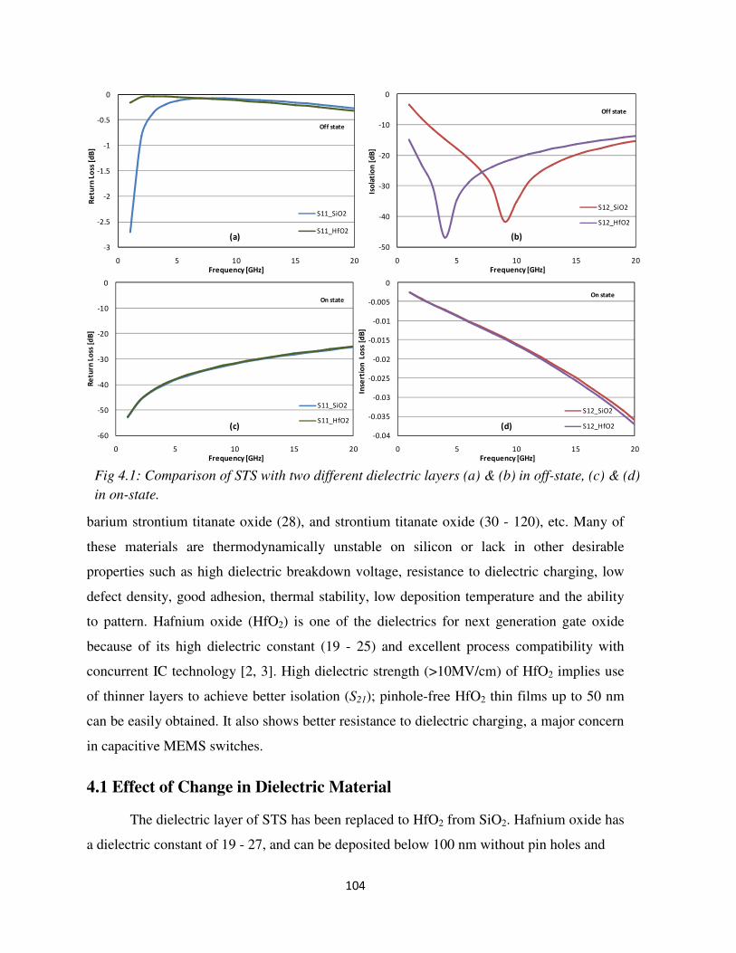
Fig 4.1: Comparison of STS with two different dielectric layers (a) & (b) in off-state, (c) & (d)
in on-state.
105
with high dielectric breakdown voltages. For the same dimensions of the Symmetric Toggle
Switch (STS), simulation and experimental study has been performed and results have been
compared. Simulated HfO2 devices show better and wide band response as compared to
SiO2 devices. Fig. 4.1 (a) - (d) shows the simulated comparison of off-state and on-state
response of STS with SiO2 and HfO2 dielectric layers. As can be seen from the plotted
curves, the curve shifts to the lower frequency side due to the incorporation of HfO2 as a
dielectric material with better isolation. As HfO2 has high dielectric constant as compared to
SiO2, the off-state and on-state capacitances are higher and thus the capacitance ratio. The
calculated capacitance ratio of HfO2 dielectric based STS is almost 10 times higher than the
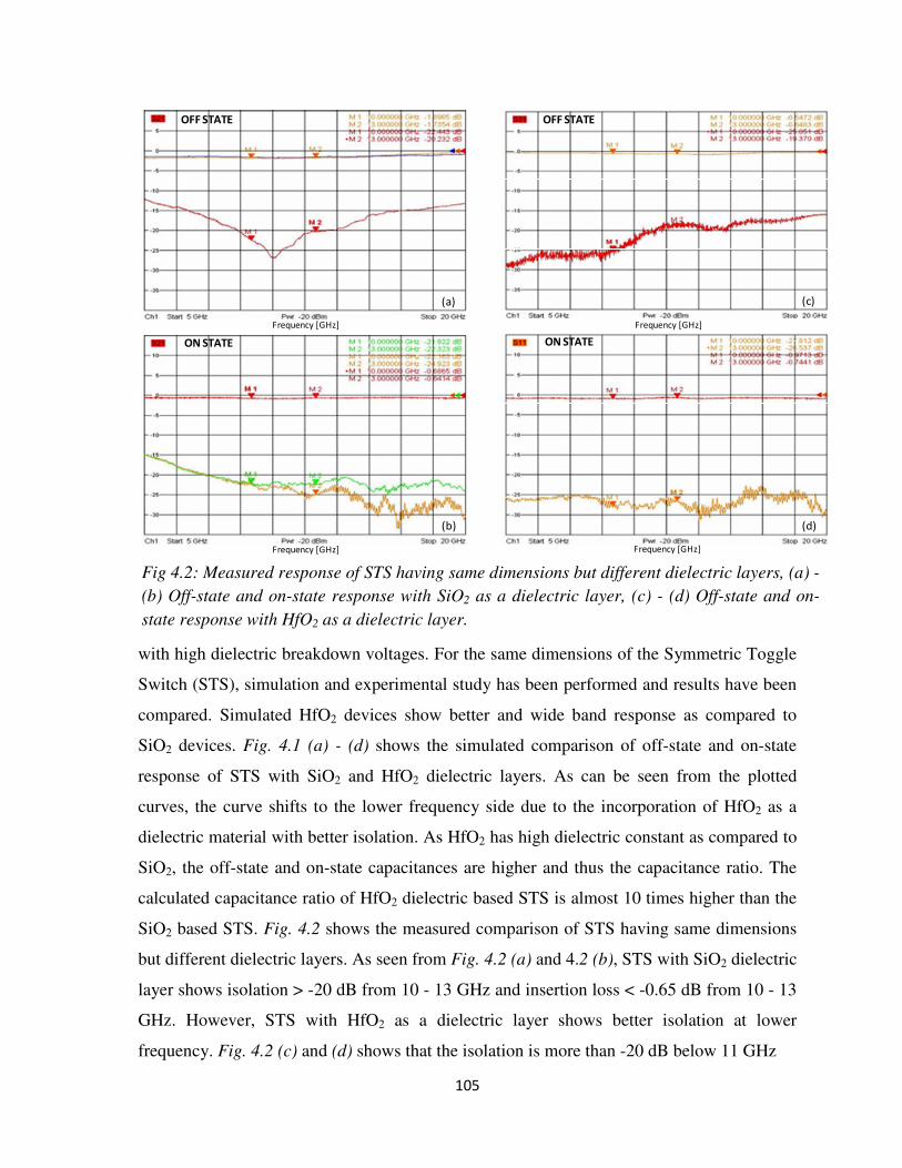
SiO2 based STS. Fig. 4.2 shows the measured comparison of STS having same dimensions
but different dielectric layers. As seen from Fig. 4.2 (a) and 4.2 (b), STS with SiO2 dielectric
layer shows isolation > -20 dB from 10 - 13 GHz and insertion loss < -0.65 dB from 10 - 13
GHz. However, STS with HfO2 as a dielectric layer shows better isolation at lower
frequency. Fig. 4.2 (c) and (d) shows that the isolation is more than -20 dB below 11 GHz
OFF STATE
ON STATE
Frequency [GHz]
Frequency [GHz]
OFF STATE
ON STATE
Frequency [GHz]
Frequency [GHz]
(a) (c)
(b) (d)
Fig 4.2: Measured response of STS having same dimensions but different dielectric layers, (a) -
(b) Off-state and on-state response with SiO2 as a dielectric layer, (c) - (d) Off-state and on-
state response with HfO2 as a dielectric layer.
106
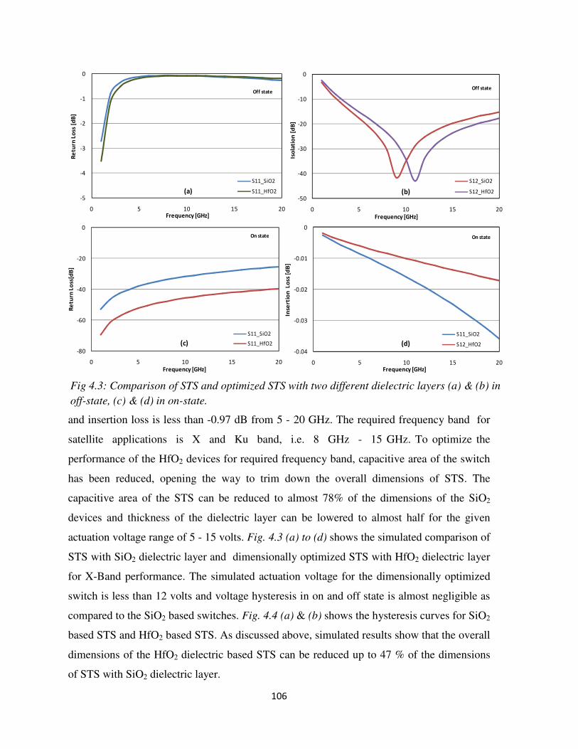
and insertion loss is less than -0.97 dB from 5 - 20 GHz. The required frequency band for
satellite applications is X and Ku band, i.e. 8 GHz - 15 GHz. To optimize the
performance of the HfO2 devices for required frequency band, capacitive area of the switch
has been reduced, opening the way to trim down the overall dimensions of STS. The
capacitive area of the STS can be reduced to almost 78% of the dimensions of the SiO2
devices and thickness of the dielectric layer can be lowered to almost half for the given
actuation voltage range of 5 - 15 volts. Fig. 4.3 (a) to (d) shows the simulated comparison of
STS with SiO2 dielectric layer and dimensionally optimized STS with HfO2 dielectric layer
for X-Band performance. The simulated actuation voltage for the dimensionally optimized
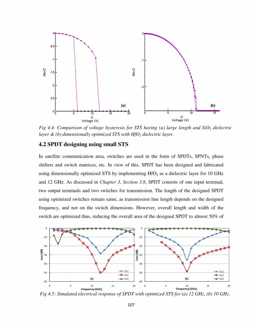
switch is less than 12 volts and voltage hysteresis in on and off state is almost negligible as
compared to the SiO2 based switches. Fig. 4.4 (a) & (b) shows the hysteresis curves for SiO2
based STS and HfO2 based STS. As discussed above, simulated results show that the overall
dimensions of the HfO2 dielectric based STS can be reduced up to 47 % of the dimensions
of STS with SiO2 dielectric layer.
-5
-4
-3
-2
-1
0
0 5 10 15 20
S11_SiO2
S11_HfO2
Frequency [GHz]
Re
turn
Lo
ss [
dB
]
(a)
Off state
Frequency [GHz]
-80
-60
-40
-20
0
0 5 10 15 20
S11_SiO2
S11_HfO2
Re
turn
Lo
ss[d
B]
On state
(c)
Frequency [GHz]
(b)-50
-40
-30
-20
-10
0
0 5 10 15 20
S12_SiO2
S12_HfO2
Iso
lati
on
[d
B]
Off state
-0.04
-0.03
-0.02
-0.01
0
0 5 10 15 20
S11_SiO2
S12_HfO2
Frequency [GHz]
Inse
rtio
n L
oss
[d
B]
On state
(d)
Fig 4.3: Comparison of STS and optimized STS with two different dielectric layers (a) & (b) in
off-state, (c) & (d) in on-state.
107
4.2 SPDT designing using small STS
In satellite communication area, switches are used in the form of SPDTs, SPNTs, phase
shifters and switch matrices, etc. In view of this, SPDT has been designed and fabricated
using dimensionally optimized STS by implementing HfO2 as a dielectric layer for 10 GHz
and 12 GHz. As discussed in Chapter 3, Section 3.8, SPDT consists of one input terminal,
two output terminals and two switches for transmission. The length of the designed SPDT
using optimized switches remain same, as transmission line length depends on the designed
frequency, and not on the switch dimensions. However, overall length and width of the
switch are optimized thus, reducing the overall area of the designed SPDT to almost 50% of
Voltage (V) Voltage (V)
(a) (b)
-60
-50
-40
-30
-20
-10
0
0 5 10 15 20
S11
S12
S13
Frequency [GHz]
Loss
[d
B]
-60
-50
-40
-30
-20
-10
0
0 5 10 15 20
S11
S12
S13
Frequency [GHz]
Loss
[d
B]
(a) (b)
Fig 4.4: Comparison of voltage hysteresis for STS having (a) large length and SiO2 dielectric
layer & (b) dimensionally optimized STS with HfO2 dielectric layer.
Fig 4.5: Simulated electrical response of SPDT with optimized STS for (a) 12 GHz, (b) 10 GHz.
108
the SiO2 based SPDT. As compared to the SPDT designed using SiO2 dielectric layer, these
SPDTs have an area of 4mm2 at 10 GHz and 6.1 mm2 at 12 GHz. Fig. 4.5 (a) & (b) shows
the simulation results of SPDT designed by using optimized STS switches for 12 GHz and
10 GHz respectively.
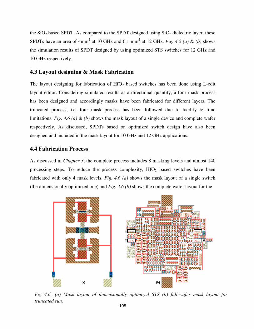
4.3 Layout designing & Mask Fabrication
The layout designing for fabrication of HfO2 based switches has been done using L-edit
layout editor. Considering simulated results as a directional quantity, a four mask process
has been designed and accordingly masks have been fabricated for different layers. The
truncated process, i.e. four mask process has been followed due to facility & time
limitations. Fig. 4.6 (a) & (b) shows the mask layout of a single device and complete wafer
respectively. As discussed, SPDTs based on optimized switch design have also been
designed and included in the mask layout for 10 GHz and 12 GHz applications.
4.4 Fabrication Process
As discussed in Chapter 3, the complete process includes 8 masking levels and almost 140
processing steps. To reduce the process complexity, HfO2 based switches have been
fabricated with only 4 mask levels. Fig. 4.6 (a) shows the mask layout of a single switch
(the dimensionally optimized one) and Fig. 4.6 (b) shows the complete wafer layout for the
(a) (b)
Fig 4.6: (a) Mask layout of dimensionally optimized STS (b) full-wafer mask layout for
truncated run.
109
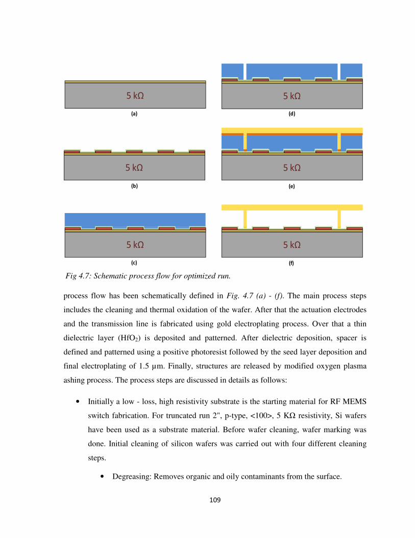
process flow has been schematically defined in Fig. 4.7 (a) - (f). The main process steps
includes the cleaning and thermal oxidation of the wafer. After that the actuation electrodes
and the transmission line is fabricated using gold electroplating process. Over that a thin
dielectric layer (HfO2) is deposited and patterned. After dielectric deposition, spacer is
defined and patterned using a positive photoresist followed by the seed layer deposition and
final electroplating of 1.5 µm. Finally, structures are released by modified oxygen plasma
ashing process. The process steps are discussed in details as follows:
• Initially a low - loss, high resistivity substrate is the starting material for RF MEMS
switch fabrication. For truncated run 2", p-type, <100>, 5 KΩ resistivity, Si wafers
have been used as a substrate material. Before wafer cleaning, wafer marking was
done. Initial cleaning of silicon wafers was carried out with four different cleaning
steps.
• Degreasing: Removes organic and oily contaminants from the surface.
5 kΩ5 kΩ
5 kΩ
5 kΩ
5 kΩ
5 kΩ
(a)
(b)
(c)
(d)
(e)
(f)
Fig 4.7: Schematic process flow for optimized run.
110
• RCA 1: Removes organic contaminants from the wafer surface.
• Piranha Cleaning: Removes heavy metal particles from the wafer surface.
• HF Dip: HF dip removes nascent oxide from the wafer surface formed during
the piranha cleaning process.
• In the next step an isolation layer of 1000 nm of silicon dioxide is grown using
thermal oxidation process (Furnace temperature: 1050˚C, for 15 minutes in N2
ambient, 155 minutes in H2O ambient and finally again 15 minutes in N2 ambient).
• The next step is to define actuation electrodes and transmission line. As the
optimized process has been planned for truncated fabrication, the actuation
electrodes and the transmission line, both have been processed in same masking level
using gold electroplating process. Before electroplating, seed layer of Ti/Au has been
sputter deposited and a photoresist mould has been made by using photolithography
process of AZ P4620 thick positive photoresist. After mold formation, 1 µm thick
electroplating has been done followed by photoresist mold removal and seed layer
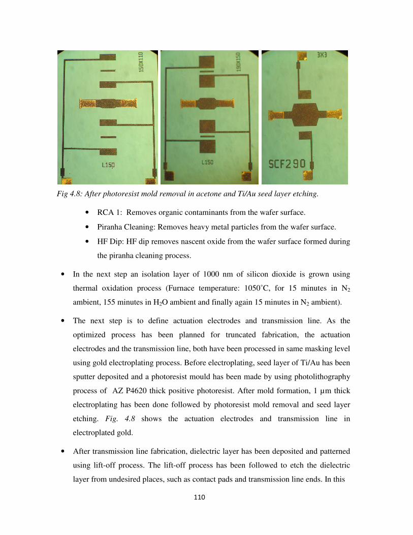
etching. Fig. 4.8 shows the actuation electrodes and transmission line in
electroplated gold.
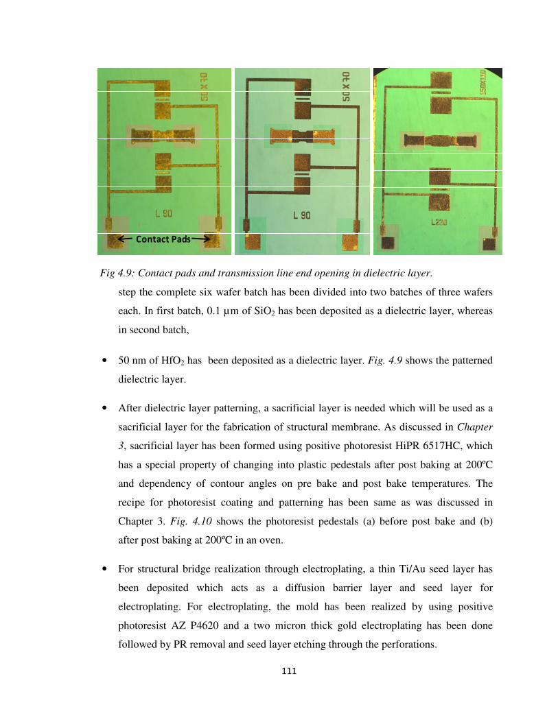
• After transmission line fabrication, dielectric layer has been deposited and patterned
using lift-off process. The lift-off process has been followed to etch the dielectric
layer from undesired places, such as contact pads and transmission line ends. In this
Fig 4.8: After photoresist mold removal in acetone and Ti/Au seed layer etching.
111
step the complete six wafer batch has been divided into two batches of three wafers
each. In first batch, 0.1 µm of SiO2 has been deposited as a dielectric layer, whereas
in second batch,
• 50 nm of HfO2 has been deposited as a dielectric layer. Fig. 4.9 shows the patterned
dielectric layer.
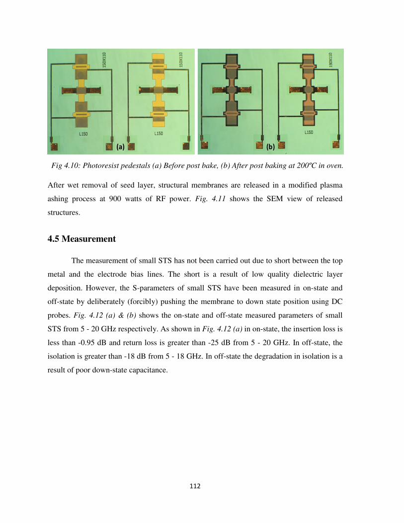
• After dielectric layer patterning, a sacrificial layer is needed which will be used as a
sacrificial layer for the fabrication of structural membrane. As discussed in Chapter
3, sacrificial layer has been formed using positive photoresist HiPR 6517HC, which
has a special property of changing into plastic pedestals after post baking at 200ºC
and dependency of contour angles on pre bake and post bake temperatures. The
recipe for photoresist coating and patterning has been same as was discussed in
Chapter 3. Fig. 4.10 shows the photoresist pedestals (a) before post bake and (b)
after post baking at 200ºC in an oven.
• For structural bridge realization through electroplating, a thin Ti/Au seed layer has
been deposited which acts as a diffusion barrier layer and seed layer for
electroplating. For electroplating, the mold has been realized by using positive
photoresist AZ P4620 and a two micron thick gold electroplating has been done
followed by PR removal and seed layer etching through the perforations.
Contact Pads
Fig 4.9: Contact pads and transmission line end opening in dielectric layer.
112
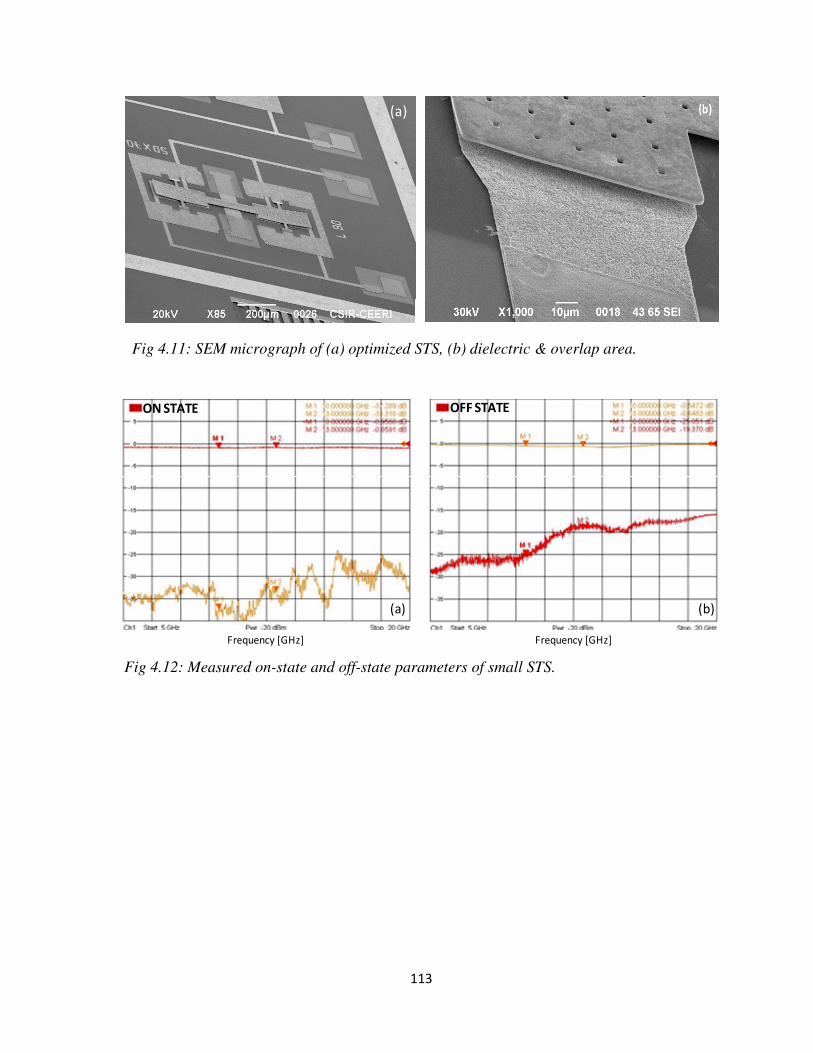
After wet removal of seed layer, structural membranes are released in a modified plasma
ashing process at 900 watts of RF power. Fig. 4.11 shows the SEM view of released
structures.
4.5 Measurement
The measurement of small STS has not been carried out due to short between the top
metal and the electrode bias lines. The short is a result of low quality dielectric layer
deposition. However, the S-parameters of small STS have been measured in on-state and
off-state by deliberately (forcibly) pushing the membrane to down state position using DC
probes. Fig. 4.12 (a) & (b) shows the on-state and off-state measured parameters of small
STS from 5 - 20 GHz respectively. As shown in Fig. 4.12 (a) in on-state, the insertion loss is
less than -0.95 dB and return loss is greater than -25 dB from 5 - 20 GHz. In off-state, the
isolation is greater than -18 dB from 5 - 18 GHz. In off-state the degradation in isolation is a
result of poor down-state capacitance.
(a) (b)
Fig 4.10: Photoresist pedestals (a) Before post bake, (b) After post baking at 200ºC in oven.
113
(b)(a)
Frequency [GHz] Frequency [GHz]
ON STATE OFF STATE
(a) (b)
Fig 4.11: SEM micrograph of (a) optimized STS, (b) dielectric & overlap area.
Fig 4.12: Measured on-state and off-state parameters of small STS.
114
References
[1]. H. A. C. Tilmans, “MEMS components for wireless communications”, in
Eurosensors XVI, 16th European Conference on Solid State Transducers, Prague,
CZ, September 15 - 18, 2002, pp. 1 - 34.
[2]. Cari F Herrmann, Frank W. DelRio, David C. Miller, Steven M. George, Victor M.
right, Jack L. Ebel, Richard E. Strawser, Rebecca Cortez, Kevin D. Leedy,
“Alternative dielectric films for rf MEMS capacitive switches deposited using
atomic layer deposited Al2O3/ZnO alloys”, Sensors and Actuaturs A, vol. 135, 2007,
pp. 262 - 272.
[3]. Jiunnjye Tsaur, Kazumasa Onodera, Takeshi Kobayashi, Zhang-Jie Wang, Sven
Heisig, Ryutaro Maeda, Tadatomo Suga, “Broadband MEMS shunt switches using
PZT-HfO2 multi-layered high k dielectric for high switching isolation”, Sensors and
Actuaturs A, vol. 121, 2005, pp. 262 - 272.
[4]. Yi Zhang, Kazumasa Onodera, Ryutaro Maeda, “RF Micro - Electro - Mechanical -
Systems Capacitive Switches Using Ultra Thin Hafnium Oxide Dielectric”, Japanese
Journal of Applied Physics, vol. 45, no. 1A, January 2006, pp. 300 - 304.
[5]. Yi Zhang, Jian Lu, Kazumasa Onodera, Ryutaro Maeda, “Development of Hafnium
Oxinitride Dielectrics for Radio - Frequency - Microelectro Mechanical System
Capacitive Switches”, Sensors and Actuators A, vol. 139, February 2007, pp. 337-
342.


![Feasibility of Using Gluconolactone, Trehalose and Hydroxy …sure.sunderland.ac.uk/8775/1/pharmaceutics-10-00022.pdf · 2018-02-23 · generic development [3]. To overcome this problem](https://img.pdfslide.us/doc/110x75/5f48b009a3bae225431a6294/feasibility-of-using-gluconolactone-trehalose-and-hydroxy-sure-2018-02-23-generic.jpg)