Embed Size (px)
Citation preview
Facoltà di Ingegneria
Dipartimento di Ingegneria dell’Informazione ed Elettrica e Matematica Applicata
Dottorato di Ricerca in Ingegneria dell’Informazione
XIV Ciclo – Nuova Serie
TESI DI DOTTORATO
Control Issues in Photovoltaic Power
Converters
CANDIDATO: MASSIMILIANO DE CRISTOFARO
COORDINATORE: PROF. MAURIZIO LONGO
TUTOR: PROF. NICOLA FEMIA
CO-TUTOR: PROF. GIOVANNI PETRONE
Anno Accademico 2014 – 2015
UNIVERSITÀ DEGLI
STUDI DI SALERNO

To my family
To my friends

Contents
Contents ................................................................... 3
Introduction ............................................................. 5
Chapter 1 Photovoltaic Inverters ........................ 10
1.1 Half-Bridge Voltage Source Inverter ........................ 11
1.2 Full-Bridge Voltage Source Inverter ........................ 12
1.3 Three-phase Voltage Source Inverter ....................... 13
1.4 Neutral point Clamped Inverter ................................ 14
1.5 αβ and dq transformations ........................................ 16
1.6 Control techniques for PV inverters ......................... 20
1.7 Maximum Power Point Tracking techniques ........... 25
References ....................................................................... 29
Chapter 2 An improved Dead-Beat control based
on an Observe&Perturb algorithm.................. 31
2.1 Description of the simulator tool .............................. 33
2.2 Standard controller design ........................................ 35 2.2.1 Proportional-Integral Linear Control design ..................... 38
2.2.2 Dead-Beat control design .................................................. 40
2.2.3 Hybrid solution: Dead-Beat and integral action ................ 45
2.3 Observe&Perturb Dead-Beat control ........................ 45
2.4 Simulation results ..................................................... 49
2.5 Implementation on a microcontroller ....................... 56
References ....................................................................... 61

4 Contents
Chapter 3 The Effect of a Constant Power Load
on the Stability of a Smart Transformer ......... 65
3.1 Constant power load characteristic and single loop
control analysis ............................................................ 68
3.2 Double loop control analysis ..................................... 79
References ....................................................................... 82
Chapter 4 Minimum Computing MPPT ............ 84
4.1 Light-to-Light system case study ................................. 86
4.2 Adaptive duty-cycle setup ............................................ 88
4.3 LED Dimming-based Bulk Voltage regulation ............ 95
4.4 Experimental results ..................................................... 98
References ......................................................................... 107
Conclusions .......................................................... 109
List of publications .............................................. 112
Acknowledgements .............................................. 113
Introduction
The development of this thesis was born from cooperation between
the Power Electronics and Renewable Sources Laboratory of the
University of Salerno and the ABB Solar Group company (ex Power-
One) of Terranuova Bracciolini (AR), Italy that is one of the most
important manufactures of Photovoltaic (PV) power converters. Its
portfolio covers all the possible PV systems: from the module (50-
400W), to the string (0.2-2kW) up to the centralized solutions (more
than 1MW).
This company has pointed out a great interest to investigate issues
related to the control of PV systems to explore new control techniques
that can have static and dynamic performance better than the existing
techniques implemented in its systems, to analyze new scenarios due
to the insertion of the Distributed Power Generating Systems (DPGSs)
into the grid and to optimize the current methods to extract power
from the PV source with the final goal to increase the performance of
the PV systems at any level, system, grid and circuit. Specifically the
progress of photovoltaic technology has opened a scenario of different
solutions:
- at system level, still today there is a high interest of the
industry for the centralized solutions in less-developing
country, such as China, India and Thailand, where the system
must work in poor grid conditions with great changes of
frequency and root-means square value and must be able to
ensure the respect of the regulation requirements during the
grid faults. So, define new current control techniques that
allow having better performance for these systems is currently
a challenge for the industry;
- at grid level, it has enabled a transition from a highly
centralized structure of electric power system, with large
capacity generators, to a new decentralized infrastructure with
the insertion of small and medium capacity generators. This
has led great changes in the electric grid. The conventional
6 Introduction
grid was composed of a source, a distribution energy system
and loads. Instead, new scenarios include the presence of
DPGSs that can inject locally energy into the grid. The study
of DPGSs is of a great interest from the point of view of the
overall system, where it is important to choice where it is
convenient to insert the DPGS, as well as from the point of
view of the local system, where there are problems to control
and synchronization. Moreover, the increase in performance,
combined with the costs reduction of solid state devices, has
led to the development and the diffusion of the power
converters with the result that, today, almost the totality of the
electrical energy is controlled by power electronic systems;
- at circuit level, the wide interest for Maximum Power Point
Tracking (MPPT) control is justified by the attempt to
maximize the energy harvested from photovoltaic sources in
all the operating conditions. Several control techniques can be
adopted, both analog and digital, to achieve good MPPT
efficiency. Digital techniques are best suited to implement
adaptive control. The runtime optimization of MPPT digital
control is in the focus of many studies, mostly regarding the
Perturb&Observe (P&O) technique. The two parameters
determining the MPPT efficiency and the tracking speed P&O
technique are the sampling period TMPPT and the duty-cycle
step perturbation magnitude ΔD. The level of MPPT efficiency
achievable by the most of the existing techniques is
conditioned by many factors, such as the modeling
assumptions, the duty-cycle and sampling period correction
law adopted, the computing capabilities of the digital device
adopted for the control implementation. To this regard, they
involve a variable amount of computations, including the
calculation of the ratios (e.g. ΔI/ΔD, ΔP/ΔV) used as figure of
merit, the subsequent calculations required by the adaptation
law, and the additional calculations required by specific
estimation/decision algorithm used. As a consequence, many
methods and algorithms yield high MPPT efficiency at the
price of high computing effort, which is not compatible with
low cost requirements. Achieving maximum energy harvesting

7 Introduction
with minimum cost devices is a fundamental renewable energy
industry demand.
Hence, there are many issues, also attractive for the scientific
field, to investigate about the design of PV systems in the present-day
evolving scenario, as it is not completely defined. For this reason,
during this study, models, methods and algorithms will be developed
to analyze these challenges at any level starting from the inputs
provided by ABB Solar Group.
The dissertation is organized as follows.
In the chapter 1, the basic circuit topologies and tools used for the
PV systems will be presented. The main aim is to explain the
operation of circuits and tools used by ABB Solar Group for its
converters and that will be used for the control issues analyzed in the
next chapters. Hence, the basic Voltage Source Inverter (VSI), single-
phase and three-phase, and the multilevel Neutral Point Clamped
(NPC) inverter will be discussed. Also very useful tools for the control
design, the αβ and dq transformations, will be summarized and, at the
end, an overview of the existing control and MPPT techniques will be
presented.
In the chapter 2, an improved Dead-Beat control based on an
Observe&Perturb (O&P) algorithm will be developed for the Neutral
Point Clamped (NPC) inverter that is the most widely used topology
of multilevel inverters for high power applications. Indeed a NPC-
based inverter, the AURORA ULTRA of 1.4MW, is developed by ABB
Solar Group mainly for the Asian market. A comprehensive
comparison between the standard Dead-Beat, the proportional-integral
and the proposed Dead-Beat control will be performed for a passive
NPC inverter. Also stability aspects for these controllers will be
analyzed and, based on that, the general guideline to select the
parameters of the proposed O&P algorithm will be defined. The
comparison will be done with a dedicated simulation tool, written in
C++ language, since the existing commercial software, such as
Simulink®, PSIM
® and PSPICE
®, allow to make the analysis only a
specific level: system, circuit or device. Both O&P method and
simulation tool are not only for NPC inverters but they are very
8 Introduction
general being able to be applied to all the converters. At the end, the
proposed O&P Dead-Beat control will be implemented on a
TMS320F28379D Dual-Core Delfino™ Microcontroller (µc) to test
the feasibility of all its components in a single embedded system. The
choice of the F28379D µc is carried out to use the same family, the TI
C2000, that ABB Solar Group implements on its converters and to
have the best performance with a dual-core system. This µc
implementation has been performed at the Texas Instruments of
Freising, Germany.
In the chapter 3, a critical scenario for the stability of the electric
grid will be investigated. It will be implemented with a Smart
Transformer (ST) that can be composed by one or more energy
conversion stages, i.e. one or more power converters, some loads and
some DPGSs directly connected to the low voltage side of the ST. The
ST is a Solid State Transformer (SST) used in electric distribution
system to provide ac bus voltages with a fixed amplitude and
frequency for each of the possible configuration of loads. The
international industry practice on load modeling for static and
dynamic power system studies will be discussed and it will be shown
that the Constant Power Load (CPL) model is mostly used (about
84%) for power system static analysis. The main characteristic of a
CPL is that its current decreases when its voltage increases and vice
versa and, so, it presents negative impedance for the small signal
analysis that can impact the system stability. For this reason, in this
chapter, the scenario with only CPLs, the worst case for the stability,
will be analyzed to verify if it is possible to use controllers usually
designed for stable systems even when the CPLs make the system
unstable. A three-phase system, composed by a Voltage Source
Inverter (VSI) with an LC filter representing the output stage of the
ST, a DC-source that represents the ST DC bulk, the CPL, the
controller and the Pulse Width Modulator (PWM) will be considered.
At the end the conditions to design the LC filter to have a stable
system with a CPL will be provided. The analysis of a system with a
CPL has been developed also in cooperation with the Chair of Power
Electronics of the Albrechts-Universität zu Kiel, Germany.
In the chapter 4, after that the methodologies to track the
Maximum Power Point (MPP) will be presented, a method to

9 Introduction
determine the sampling period TMPPT and the duty-cycle step
perturbation magnitude ΔD will be developed. This realizes the real
time adaptation of a photovoltaic P&O MPPT control with minimum
computing effort to maximize the PV energy harvesting against
changes of sun irradiation, the temperature and the characteristics of
the PV source and by the overall system the PV source is part of. It
exploits the correlation existing among the MPPT efficiency and the
onset of a permanent 3 level quantized oscillation around the MPP. A
comparison between an existing adaptive MPPT algorithm will be
performed through simulations, to set exactly the same test conditions
and, after, as a multifunction control application case study, a
TMS320F28035 Texas Instruments Piccolo™ Microcontroller will be
used to implement the proposed adaptive PV MPPT control algorithm
on a 70W LED lighting system prototype fed by a photovoltaic
source, with a capacitor working as storage device. The choice of the
F28035 µc is carried out to use the same family, the TI C2000, that
ABB Solar Group implements on its converters but with a single-core
system as the goal of the proposed method is the minimum computing
effort. Hence the aim of this chapter is to determine an optimize
MPPT algorithm that can be implemented in the ABB Solar Group
systems.
Chapter 1
Photovoltaic Inverters
The PV inverter is the main element of grid-connected PV power
systems: it converts the power from the PV source into the AC grids.
The development of the circuit topologies for the PV inverters has had
as principal goal to maximize the efficiency but other complex
functions, usually not present in motor drive inverters, are typically
required like the maximum power point tracking, anti-islanding and
grid synchronization [1]. To have an increment of the efficiency, the
galvanic isolation typically provides by high-frequency transformers
in the DC/DC boost converter or by a low-frequency transformer on
the output has been eliminated. But the transformerless structure
typically requires more complex solutions to keep the leakage current
and DC current injection under control in order to comply with the
safety issues resulting in novel topologies. These topologies have been
taking the starting point from two converter families: H-bridge and
Neutral Point Clamped (NPC) that are the most suitable respectively
for low power inverter (up to tens of kW) and for high power inverters
(hundreds of kW) [1].
The aim of this chapter is to explain the operation of the basic
circuits, H-bridge and NPC, and to introduce very useful tools for the
control design of these inverters, the αβ and dq transformations. Also,
at the end, an overview of the exiting control and Maximum Power
Point Tracking (MPPT) techniques is presented.
These circuits, tools and control techniques, all used by ABB Solar
Group in its converts, represent the starting points for the control
issues addressed in the next chapters.

11 Chapter 1 Photovoltaic Inverter
1.1 Half-Bridge Voltage Source Inverter
The figure 1.1 shows the power topology of a half-bridge VSI [2],
where two capacitors (C+ and C-) are required to provide a neutral
point N, such that each capacitor maintains a constant voltage vi/2.
Because the current harmonics injected by the operation of the
inverter are low-order harmonics, a set of large capacitors is required.
It is clear that both switches S+ and S- cannot be ON
simultaneously because a short circuit across the dc link voltage
source vi would be produced. There are two defined (states 1 and 2)
and one undefined (state 3) switch states as shown in the table 1.1. In
order to avoid the short circuit across the dc bus and the undefined ac
output voltage condition, the modulating technique should always
ensure that at any instant either the top or the bottom switch of the
inverter leg is ON [3].
Fig 1.1 Single-phase half bridge VSI
State vo Components
Conducting
S+ is ON and S- is OFF v+/2 S+ if io>0
D+ if io<0
S- is ON and S+ is OFF -vi/2 S- if io>0
D- if io<0
S+ and S- are all OFF vi/2
- vi/2
D+ if io>0
D- if io<0
Table 1.1 Switch states for a half-bridge single-phase VSI
12 Chapter 1 Photovoltaic Inverter
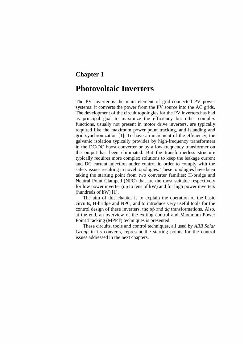
1.2 Full-Bridge Voltage Source Inverter
The figure 1.2 shows the power topology of a full-bridge VSI [2]. This
inverter is similar to the half-bridge inverter but a second leg provides
the neutral point N to the load. Both switches S1+ and S1- (or S2+ and
S2-) cannot be ON simultaneously because a short circuit across the dc
link voltage source vi would be produced. The table 1.2 shows the
possible five states of this circuit: four defined and one undefined.
The modulation technique, ensuring that either the top or the
bottom switch of each leg is ON at any instant, avoids the short circuit
across the dc bus and the undefined ac output voltage condition.
Looking at the tables 1.2 and 1.1, it is possible to notice that the ac
output voltage for the full-bridge can take values up to the dc link
value vi, while the half-bridge can reach vi/2. [3].
Fig 1.2 Single-phase full bridge VSI
State va vb vo Components Conducting
S1+ and S2- are ON and S1- and S2+ are OFF vi/2 -vi/2 vi S1+ and S2- if io>0
D1+ and D2- if io<0
S1- and S2+ are ON and S1+ and S2- are OFF -vi/2 vi/2 -vi S1- and S2+ if io>0
D1- and D2+ if io<0
S1+ and S2+ are ON and S1- and S2- are OFF vi/2 vi/2 0 S1+ and S2+ if io>0
D1+ and D2+ if io<0
S1- and S2- are ON and S1+ and S2+ are OFF -vi/2 -vi/2 0 S1- and S2- if io>0
D1- and D2- if io<0
S1+, S2+, S1- and S2- are all OFF -vi/2
vi/2
vi/2
-vi/2
- vi
vi
D1- and D2+ if io>0
D1+ and D2- if io<0
Table 1.2 Switch states for a full-bridge single-phase VSI
13 Chapter 1 Photovoltaic Inverter
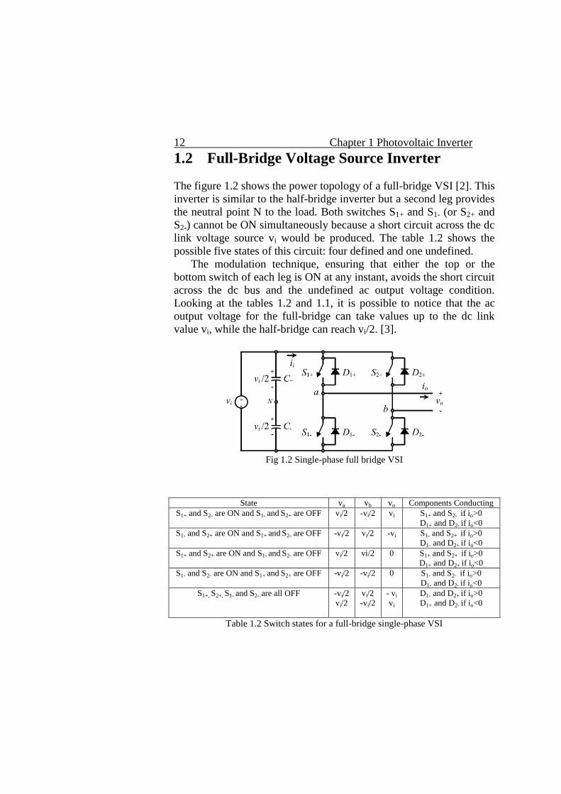
1.3 Three-phase Voltage Source Inverter
The single-phase VSIs cover low-range power applications while the
three-phase VSIs cover the medium to high-power applications (from
few hundreds of kW) [2]. The main purpose of these topologies is to
provide a three-phase voltage source, where the amplitude, phase, and
frequency of the voltages should always be controllable. Although
most of the applications require sinusoidal voltage waveforms,
arbitrary voltages are also required in some emerging applications
(e.g. active filters, voltage compensators).
The standard three-phase VSI topology is shown in the figure 1.3
and the eight valid switch states are given in the table 1.3 based on the
same considerations for the single-phase VSIs described in the
previous sections. Of the eight valid states, two of them (7 and 8 in the
table 1.3) produce zero ac line voltages. In this case, the ac line
currents freewheel through either the upper or lower components. The
remaining states (1 to 6 in table 1.3) produce no-zero ac output
voltages. In order to generate a given voltage waveform, the inverter
moves from one state to another. Thus the resulting ac output line
voltages consist of discrete values of voltages that are vi, 0, and -vi for
the topology considered. [3].
Fig 1.3 Three-phase VSI

14 Chapter 1 Photovoltaic Inverter
State vab vb va
1. S1, S2 and S6 are ON and S4, S5 and S3 are OFF vi 0 -vi
2. S2, S3 and S1 are ON and S5, S6 and S4 are OFF 0 vi - vi
3. S3, S4 and S2 are ON and S6, S1 and S5 are OFF - vi vi 0
4. S4, S5 and S3 are ON and S1, S2 and S6 are OFF - vi 0 vi
5. S5, S6 and S4 are ON and S2, S3 and S1 are OFF 0 - vi vi
6. S6, S1 and S5 are ON and S3, S4 and S2 are OFF vi - vi 0
7. S1, S3 and S5 are ON and S4, S6 and S2 are OFF 0 0 0
8. S4, S6 and S2 are ON and S1, S3 and S5 are OFF 0 0 0
Table 1.3 Valid switch states for a three-phase VSI
1.4 Neutral point Clamped Inverter
The multilevel inverter has been developed to improve the
performance of the two levels inverters and has become more and
more interesting with the continuous evolution of the power switches
in term of voltage and current rating and price [3].
A multilevel inverter that has the same voltages and powers of a
two levels inverter has a better voltages harmonic spectrum so it is
simpler to respect the law requirements. Indeed, having more levels, it
is able to reproduce voltage and current waveforms more similar to a
sinusoidal one and so the load absorbs fewer harmonic.
The principal effects of the harmonic reductions into the current
loads are:
less power losses in the iron and copper
less electromagnetic interferences (EMIs)
less mechanical oscillations in motor loads
The Neutral Point Clamped (NPC) inverter is the most extensively
applied multilevel converter topology at present [3]. A three-level
NPC inverter is illustrated in the figure 1.4, which is able to provide
five-level-step-shaped line to line voltage (three-level-step-shaped
phase voltage) without transformers or reactors and so it can reduce
harmonics in both of the output voltage and current. The main benefit
of this configuration is that each of the switches must block only half
15 Chapter 1 Photovoltaic Inverter
of the dc-link voltage Vdc even if their number is twice of a two-level
inverter. However, the NPC inverter has some drawbacks, such as
additional clamping diodes, a complex Pulse Width Modulation
(PWM) switching pattern design and a possible deviation of Neutral
Point (NP) voltage. In addition, since the NPC inverter is mostly used
for medium or high-power applications, the minimization of the
switching losses is such a relevant issue. As to the modulation
strategies, three popular modulation techniques for NPC inverters,
Carrier-Based (CB) PWM, Space Vector Modulation (SVM) and
Selective Harmonic Elimination (SHE), have been widely used in
practice. The SHE method shows an advantage for high-power
applications due to having a small number of switching actions. The
other two PWM techniques are commonly used in various
applications because of their high PWM qualities [3].
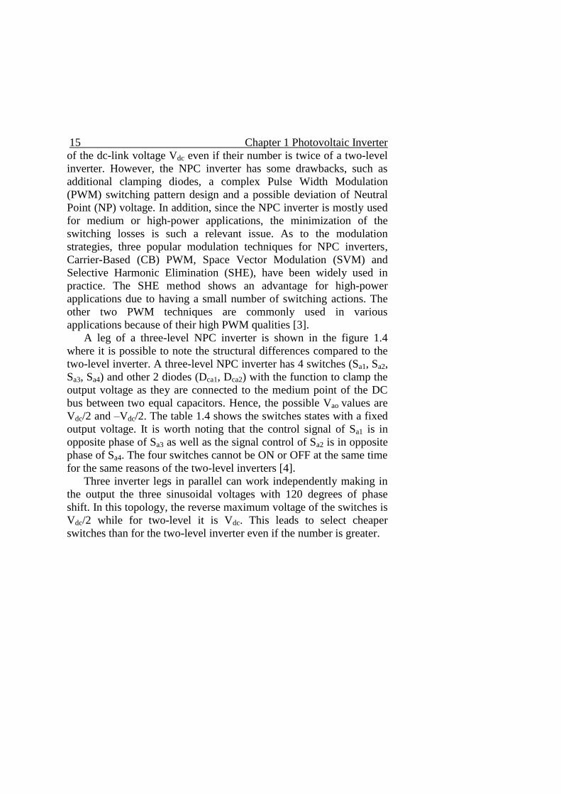
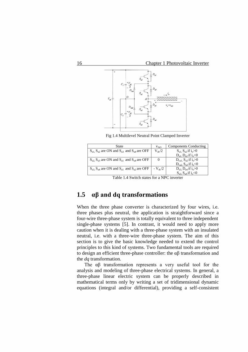
A leg of a three-level NPC inverter is shown in the figure 1.4
where it is possible to note the structural differences compared to the
two-level inverter. A three-level NPC inverter has 4 switches (Sa1, Sa2,
Sa3, Sa4) and other 2 diodes (Dca1, Dca2) with the function to clamp the
output voltage as they are connected to the medium point of the DC
bus between two equal capacitors. Hence, the possible Vao values are
Vdc/2 and –Vdc/2. The table 1.4 shows the switches states with a fixed
output voltage. It is worth noting that the control signal of Sa1 is in
opposite phase of Sa3 as well as the signal control of Sa2 is in opposite
phase of Sa4. The four switches cannot be ON or OFF at the same time
for the same reasons of the two-level inverters [4].
Three inverter legs in parallel can work independently making in
the output the three sinusoidal voltages with 120 degrees of phase
shift. In this topology, the reverse maximum voltage of the switches is
Vdc/2 while for two-level it is Vdc. This leads to select cheaper
switches than for the two-level inverter even if the number is greater.
16 Chapter 1 Photovoltaic Inverter
Fig 1.4 Multilevel Neutral Point Clamped Inverter
State vAO Components Conducting
Sa1, Sa2 are ON and Sa3 and Sa4 are OFF Vdc/2 Sa1, Sa2 if io>0
Da1, Da2 if io<0
Sa2, Sa3 are ON and Sa1 and Sa4 are OFF 0 Dca1, Sa2 if io>0
Dca2, Sa3 if io<0
Sa3, Sa4 are ON and Sa1 and Sa2 are OFF - Vdc/2 Da3, Da4 if io>0
Sa3, Sa4 if io<0
Table 1.4 Switch states for a NPC inverter
1.5 αβ and dq transformations
When the three phase converter is characterized by four wires, i.e.
three phases plus neutral, the application is straightforward since a
four-wire three-phase system is totally equivalent to three independent
single-phase systems [5]. In contrast, it would need to apply more
caution when it is dealing with a three-phase system with an insulated
neutral, i.e. with a three-wire three-phase system. The aim of this
section is to give the basic knowledge needed to extend the control
principles to this kind of systems. Two fundamental tools are required
to design an efficient three-phase controller: the αβ transformation and
the dq transformation.
The αβ transformation represents a very useful tool for the
analysis and modeling of three-phase electrical systems. In general, a
three-phase linear electric system can be properly described in
mathematical terms only by writing a set of tridimensional dynamic
equations (integral and/or differential), providing a self-consistent

17 Chapter 1 Photovoltaic Inverter
mathematical model for each phase. In some cases though, the
existence of physical constraints makes the three models not
independent from each other. In these circumstances the order of the
mathematical model can be reduced, from three to two dimensions,
without any loss of information. As it is meaningful to reduce the
order of the mathematical model, the αβ transformation represents the
most commonly used relation to perform this reduction [5].
Considering a tridimensional vector xabc = [xa xb xc]T that can be
any triplet of the system electrical variables, voltages or currents, it is
possible to introduce the linear transformation, Tαβγ:
1 112 2
20 3 2 3 2
31 1 1
2 2 2
a a
b b
c c
x x x
x T x x
x xx
(1.1)
which, in geometrical terms, represents a change from the set of
reference axes denoted as abc to the equivalent one indicated as αβγ.
The Tαβγ transformation has the following interesting property:
0 0a b cx x x x
(1.2)
Every time the constraint (1.2) is valid for a tridimensional system, the
coordinate transformation Tαβγ allows describing the same system in a
bidimensional space without any loss of information.
Considering a triplet of symmetric sinusoidal signals:
sin
sin 2 3
sin 2 3
a M
b M
c M
e U t
e U t
e U t
(1.3)
it is easy to verify that
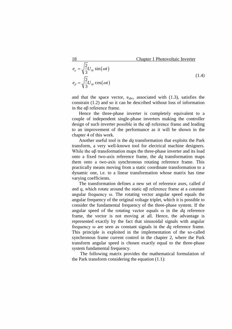
18 Chapter 1 Photovoltaic Inverter
2sin
3
2cos
3
M
M
e U t
e U t
(1.4)
and that the space vector, eabc, associated with (1.3), satisfies the
constrain (1.2) and so it can be described without loss of information
in the αβ reference frame.
Hence the three-phase inverter is completely equivalent to a
couple of independent single-phase inverters making the controller
design of such inverter possible in the αβ reference frame and leading
to an improvement of the performance as it will be shown in the
chapter 4 of this work.
Another useful tool is the dq transformation that exploits the Park
transform, a very well-known tool for electrical machine designers.
While the αβ transformation maps the three-phase inverter and its load
onto a fixed two-axis reference frame, the dq transformation maps
them onto a two-axis synchronous rotating reference frame. This
practically means moving from a static coordinate transformation to a
dynamic one, i.e. to a linear transformation whose matrix has time
varying coefficients.
The transformation defines a new set of reference axes, called d
and q, which rotate around the static αβ reference frame at a constant
angular frequency ω. The rotating vector angular speed equals the
angular frequency of the original voltage triplet, which it is possible to
consider the fundamental frequency of the three-phase system. If the
angular speed of the rotating vector equals ω in the dq reference
frame, the vector is not moving at all. Hence, the advantage is
represented exactly by the fact that sinusoidal signals with angular
frequency ω are seen as constant signals in the dq reference frame.
This principle is exploited in the implementation of the so-called
synchronous frame current control in the chapter 2, where the Park
transform angular speed is chosen exactly equal to the three-phase
system fundamental frequency.
The following matrix provides the mathematical formulation of
the Park transform considering the equation (1.1):

19 Chapter 1 Photovoltaic Inverter
cos sin
sin cos
d
dq
q
x x xT
x x x
(1.5)
The two system dynamic equations are complicated by the cross-
coupling of the two axes, i.e. they are no longer independent from
each other. This is the reason why, decoupling feed-forward paths are
usually included in the control scheme making the system dynamic
totally identical to those of the original one.
To complete the discussion of the Park transform, it worth be noted
that it is also possible to implement the so-called inverse sequence
Park transform where the direction of the dq axes rotation is assumed
to be inverted, while the transformation (1.5) can be identified as the
direct sequence Park transform. This inverse transformation could be
required when the system is unbalanced and asymmetrical as
impedance unbalances and/or asymmetric voltage sources can be
found. In this case, a three-phase system can be shown to be
equivalent to the superposition of a direct sequence system and an
inverse sequence system, both of them symmetrical and balanced and
so both properly describable in the this reference.
Also, because the elements of Tdq are not time invariant, the
application of the Park transform, differently from the αβ
transformation, affects the system dynamics: any controller, designed
in the dq reference frame, is actually equivalent to a stationary frame
controller that does not maintain the same frequency response.
.
20 Chapter 1 Photovoltaic Inverter
1.6 Control techniques for PV inverters
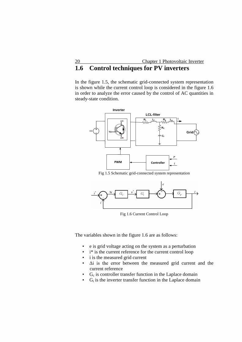
In the figure 1.5, the schematic grid-connected system representation
is shown while the current control loop is considered in the figure 1.6
in order to analyze the error caused by the control of AC quantities in
steady-state condition.
LCL-filter
ControllerPWM
i*
i
RL Lf
Cf
RC
i
DC
Inverter
Rg Lg
Grid
Fig 1.5 Schematic grid-connected system representation
Fig 1.6 Current Control Loop
The variables shown in the figure 1.6 are as follows:
• e is grid voltage acting on the system as a perturbation
• i* is the current reference for the current control loop
• i is the measured grid current
• Δi is the error between the measured grid current and the
current reference
• Gc is controller transfer function in the Laplace domain
• Gi is the inverter transfer function in the Laplace domain

21 Chapter 1 Photovoltaic Inverter
• Gp is the plant transfer function in the Laplace domain, which
is usually composed by the output filter of the converter and
the grid impedance
• v* is the controller output voltage
It has been demonstrated [6] that the grid connected LCL filter can be
regarded as an inductance for low frequencies. So it is possible to
define:
1( )pG s
Ls R
(1.6)
where L and R are respectively the filter inductance and its parasitic
resistance.
Indicating Ts the sampling time of a typical digital system, Gi is the
delay due to elaboration of the computation device (typically 1Ts) and
to the PWM (typically 0.5Ts) [1]:
1( )
1.5 1iG s
Ts
(1.7)
Hence, the current error produced by the perturbations e is:
( )( ) ( )
1 ( ) ( ) ( )
p
i
c i p
G ss e s
G s G s G s
(1.8)
The controller goal is to minimize the steady-state current error Δi(s).
There are several strategies for the control of the AC current in the
case of Distributed Power Generation Systems (DPGSs). A very
common technique used for three-phase systems is the dq control,
synchronous rotating dq reference frame based on the dq
transformation introduced in the former section. This technique is
currently used by ABB Solar Group for its three-phase inverters.
However, the dq control strategy cannot be implemented for a single-
phase system [1] unless an imaginary circuit is coupled to the real one
to simulate a two-axis environment [7]. Several controllers, such as
PI, Resonant and Dead-Beat, can be considered in order to control the
22 Chapter 1 Photovoltaic Inverter
current in the case of DPGSs. In the situation when the control
strategy is implemented in the stationary reference frame, the use of
the classical PI control leads to unsatisfactory current regulation since
the PI control are designed in order to control DC quantities which are
present only in the rotating reference frame [1].
The PI current controller GPI is defined as:
( ) IPI P
kG s k
s
(1.9)
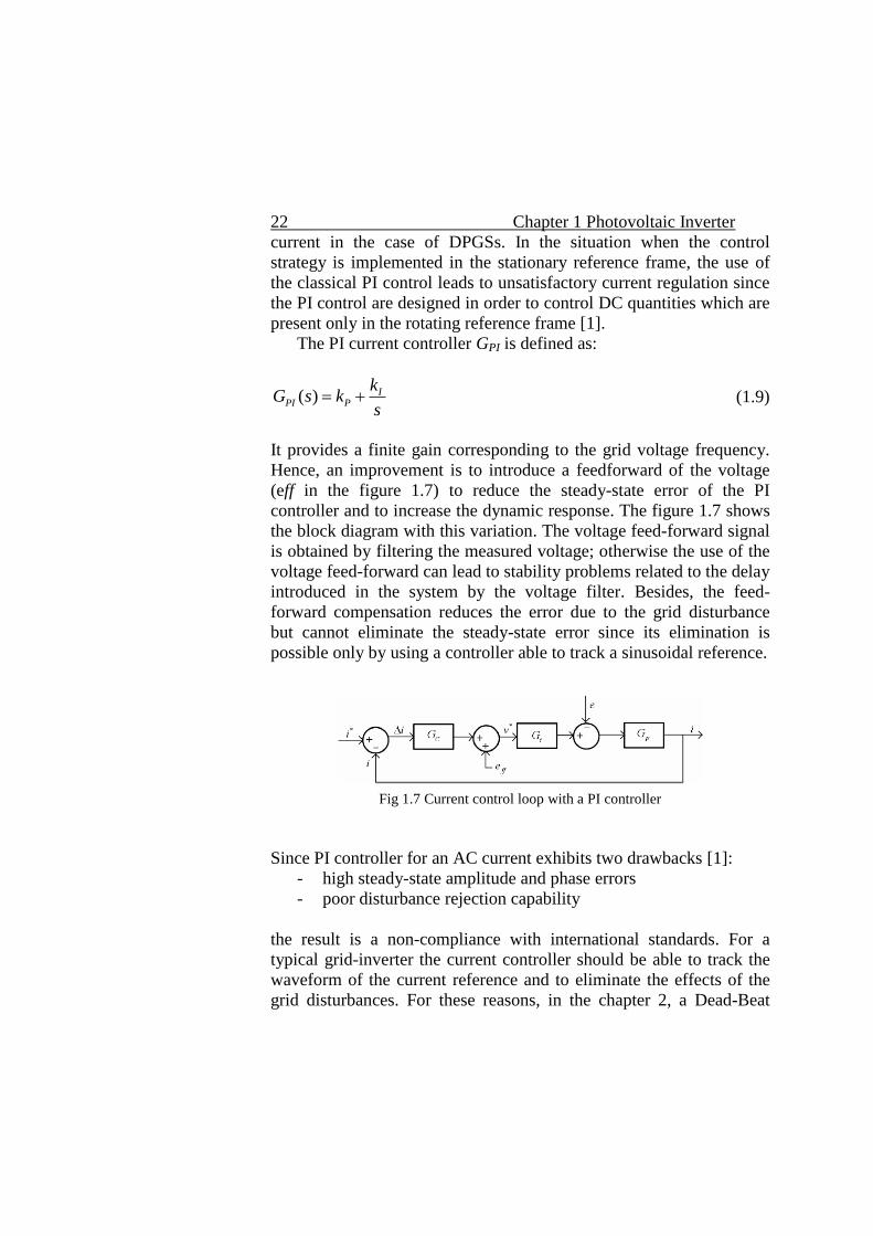
It provides a finite gain corresponding to the grid voltage frequency.
Hence, an improvement is to introduce a feedforward of the voltage
(eff in the figure 1.7) to reduce the steady-state error of the PI
controller and to increase the dynamic response. The figure 1.7 shows
the block diagram with this variation. The voltage feed-forward signal
is obtained by filtering the measured voltage; otherwise the use of the
voltage feed-forward can lead to stability problems related to the delay
introduced in the system by the voltage filter. Besides, the feed-
forward compensation reduces the error due to the grid disturbance
but cannot eliminate the steady-state error since its elimination is
possible only by using a controller able to track a sinusoidal reference.
Fig 1.7 Current control loop with a PI controller
Since PI controller for an AC current exhibits two drawbacks [1]:
- high steady-state amplitude and phase errors
- poor disturbance rejection capability
the result is a non-compliance with international standards. For a
typical grid-inverter the current controller should be able to track the
waveform of the current reference and to eliminate the effects of the
grid disturbances. For these reasons, in the chapter 2, a Dead-Beat
23 Chapter 1 Photovoltaic Inverter
technique based on an Observe&Perturb algorithm will be presented
and the design of the Dead-Beat control will be discuss in detail.
Another technique, the Resonant control, includes in the
controller a model of the reference signal and external disturbances so
robust tracking and disturbances rejection are achieved, as stated by
the Internal Model Principle (IMP) [8].
In the hypothesis of neglecting the grid voltage harmonics, the grid
voltage e can be defined as:
2 2
( )( )
( )
E
E
N se s k
D s s
(1.10)
where NE and DE are the numerator and denominator of e and k is the
grid voltage amplitude. Including DE in the generic form of the
controller Gc:
( )( )
( ) ( )
cc
c E
N sG s
D s D s
(1.11)
it results that the expression of the error Δi produced by the
perturbation e, equation (1.5), can be expressed as:
( ) ( ) ( ) ( )
( )( ) ( ) ( ) ( ) ( ) ( ) ( )
P c i Ei
P c i E P c i
N s D s D s N ss
D s D s D s D s N s N s N s
(1.12)
where Np and Dp are the numerator and denominator of Gp and Nc and
Dc are the numerator and denominator of Gc. If Nc and Dc are able to
ensure that the overall system is stable, it can be seen that Δi(t)
converges to zero when t → ∞ .
Hence, the P+Resonant regulator is defined as:
Re 2 2( )P s P I
sC s k k
s
(1.13)
24 Chapter 1 Photovoltaic Inverter
where kp and ki are the proportional and resonant gain and s/(s2+1) is
the generalized integrator (GI). kp is tuned in order to ensure that the
overall system has a specific second-order response in terms of rise
time, settling time and maximum overshoot since the size of the
proportional gain kp determines the bandwidth and the stability
margins [1], [9], [10], in the same way as in the PI controller.
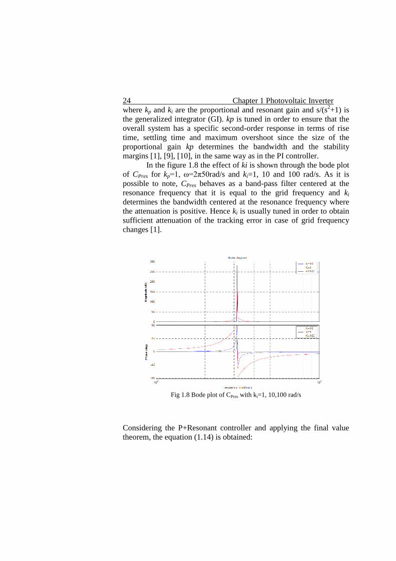
In the figure 1.8 the effect of ki is shown through the bode plot
of CPres for kp=1, ω=2π50rad/s and ki=1, 10 and 100 rad/s. As it is
possible to note, CPres behaves as a band-pass filter centered at the
resonance frequency that it is equal to the grid frequency and ki
determines the bandwidth centered at the resonance frequency where
the attenuation is positive. Hence ki is usually tuned in order to obtain
sufficient attenuation of the tracking error in case of grid frequency
changes [1].
Fig 1.8 Bode plot of CPres with ki=1, 10,100 rad/s
Considering the P+Resonant controller and applying the final value
theorem, the equation (1.14) is obtained:
25 Chapter 1 Photovoltaic Inverter
2 2
2 2 2 20
0.5 1lim 0
0.5 1sP I P
k s Tss
Ls R s Ts k s k s k
(1.14)
Hence, it can be proven that, with e(s)=0, Δi(t) converges to zero
when t → ∞ . The GI achieves an infinite gain at the resonant
frequency, so the current reference tracking is ensured setting the
resonant frequency of the controller to the fundamental frequency [11-
13].
The P+Resonant controller will be used in the chapter 3 to
analyze a critical scenario for the stability of the electric grid with a
constant power load (CPL).
1.7 Maximum Power Point Tracking techniques
The maximum power point tracking (MPPT) control can be achieved
with a number of different techniques, each one differing from the
other for complexity, robustness, static and dynamic performance. To
compare the different techniques it is possible to use the efficiency
that can be defined as “the ratio between the energy extracted from the
output terminals of a photovoltaic field and the energy really
available” [14]. The available power depends on the solar irradiation
while the extracted power depends on the impedance matching
between source and load.
The Perturb and Observe (P&O) is the most widespread technique
thanks to its simplicity and cost-effectiveness and also ABB Solar
Group usually implements this technique in its converters. It
implements a fixed-step hill climbing technique and, in the basic
version, a fixed-amplitude perturbation of the duty-cycle (ΔD) is
introduced by the controller at a fixed time step Ta. Varying the
converter duty cycle the system operation point changes and
consequently the output power extracted by the photovoltaic source.
In order to calculate the actual output power P[kTa], it is necessary to
measure the voltage and the current of the panel. This power is
compared to the value obtained from the last measurement P[(k-1)Ta].
If (P[kTa]-P[(k-1)Ta]) is positive, the controller keeps changing the
duty cycle in the same direction. When (P[kTa]- P[(k-1)Ta]) is
26 Chapter 1 Photovoltaic Inverter
negative the duty cycle change is reversed. The control algorithm can
be summarized by the following equation [15]:
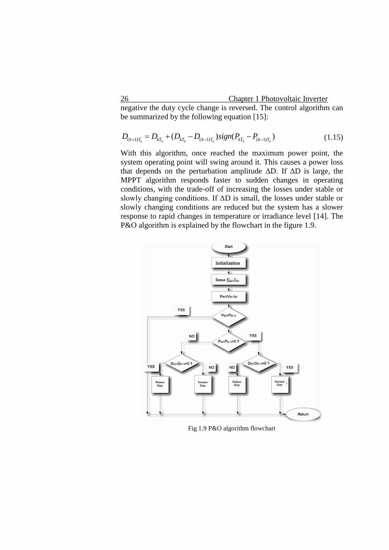
( 1) ( 1) ( 1)( ) ( )a a a a a ak T kT kT k T kT k TD D D D sign P P (1.15)
With this algorithm, once reached the maximum power point, the
system operating point will swing around it. This causes a power loss
that depends on the perturbation amplitude ΔD. If ΔD is large, the
MPPT algorithm responds faster to sudden changes in operating
conditions, with the trade-off of increasing the losses under stable or
slowly changing conditions. If ΔD is small, the losses under stable or
slowly changing conditions are reduced but the system has a slower
response to rapid changes in temperature or irradiance level [14]. The
P&O algorithm is explained by the flowchart in the figure 1.9.
Fig 1.9 P&O algorithm flowchart
27 Chapter 1 Photovoltaic Inverter
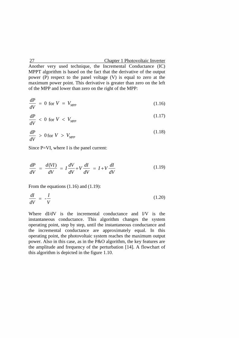
Another very used technique, the Incremental Conductance (IC)
MPPT algorithm is based on the fact that the derivative of the output
power (P) respect to the panel voltage (V) is equal to zero at the
maximum power point. This derivative is greater than zero on the left
of the MPP and lower than zero on the right of the MPP:
0dP
dV for MPPV V
(1.16)
0dP
dV for MPPV V
(1.17)
0dP
dV for MPPV V
(1.18)
Since P=VI, where I is the panel current:
( )
dP d VI dV dI dII V I V
dV dV dV dV dV
(1.19)
From the equations (1.16) and (1.19):
-dI I
dV V
(1.20)
Where dI/dV is the incremental conductance and I/V is the
instantaneous conductance. This algorithm changes the system
operating point, step by step, until the instantaneous conductance and
the incremental conductance are approximately equal. In this
operating point, the photovoltaic system reaches the maximum output
power. Also in this case, as in the P&O algorithm, the key features are
the amplitude and frequency of the perturbation [14]. A flowchart of
this algorithm is depicted in the figure 1.10.
28 Chapter 1 Photovoltaic Inverter
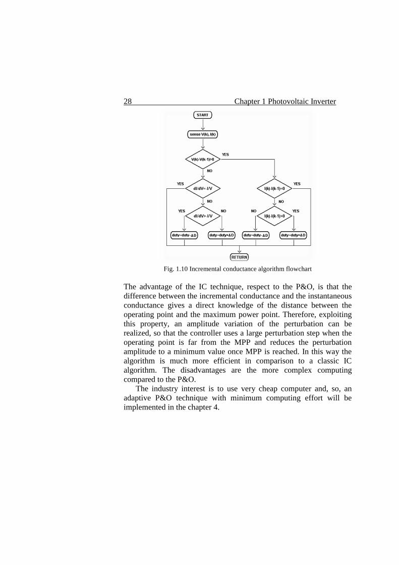
Fig. 1.10 Incremental conductance algorithm flowchart
The advantage of the IC technique, respect to the P&O, is that the
difference between the incremental conductance and the instantaneous
conductance gives a direct knowledge of the distance between the
operating point and the maximum power point. Therefore, exploiting
this property, an amplitude variation of the perturbation can be
realized, so that the controller uses a large perturbation step when the
operating point is far from the MPP and reduces the perturbation
amplitude to a minimum value once MPP is reached. In this way the
algorithm is much more efficient in comparison to a classic IC
algorithm. The disadvantages are the more complex computing
compared to the P&O.
The industry interest is to use very cheap computer and, so, an
adaptive P&O technique with minimum computing effort will be
implemented in the chapter 4.
29 Chapter 1 Photovoltaic Inverter
References
[1] Teodorescu R., Liserre M., Rodriguez P., “Grid Converters for
Photovoltaic and Wind Power System”, IEEE Press, WILEY
[2] Ned Mohan, Tore M. Undeland, William P. Robbins “Power
Electronics: Converters, Applications, and Design,” Wiley&Sons
INC.
[3] Editor in Chief Muhammad H. Rashid “Power Electronics
Handbook” Academic Press
[4] Nabae, A.; Takahashi, I.; Akagi, H., "A New Neutral-Point-
Clamped PWM Inverter," IEEE Transactions on Industry
Applications, vol. IA-17, no.5, pp.518,523, Sept. 1981
[5] S. Buso, P. Mattarelli, “Digital Control in Power Electronics”,
Morgan&Claypool Publishers
[6] K. Zhou, Kay-Soon Low, D. Wang, Fang-Lin Luo, B. Zhang,
Y.Wang, “Zero-Phase Odd-Harmonic Repetitive Controller for a
Single-Phase PWM Inverter”, IEEE Transactions on Power
Electronics, vol. 21, no. 1, Jan. 2006, pp.193-201.
[7] R. Zhang, M. Cardinal, P. Szczesny, Dame, "A grid simulator with
control of single-phase power converters in D-Q rotating frame,"
33rd Annual IEEE Power Electronics Specialists Conference,
2002, vol.3, pp. 1431-1436.
[8] B.A. Francis and W.M. Wonham, “The Internal Model Principle
for Linear Multivariable Regulators”, Appl. Math. Opt., 1975,
pp.107-194.
[9] R.W. Erickson, D. Maksimovic, “Fundamentals of Power
Electronics”, Second Edition, Springer-Verlag.
[10] W. S. Levine, “The Control Handbook: Control System
Fundamentals”, Second Edition, CRC Press
30 Chapter 1 Photovoltaic Inverter
[11] R. Teodorescu, F. Blaabjerg, U. Borup, M. Liserre, “A New
Control for Grid-Connected LCL PV Inverters with Zero Steady-
State Error and Selective Harmonic Compensation”, Proc. of
Applied Power Electronics Conference and Exposition, APEC
2004, vol. 1, pp. 580-586.
[12] D. N. Zmood, D.G. Holmes, “Stationary frame current regulation
of PWM inverters with zero steady-state error”, IEEE
Transactions on Power Electronics, vol. 18, no. 3, May 2003,
pp.814-822.
[13] Y. Sato, T. Ishizuka, K. Nezu, T. Kataoka, “A New Control
Strategy For Voltage-Type PWM Rectifiers To Realize Zero
Steady-State Control Error in Input Current”, IEEE Transactions
on Industry Applications, vol. 34, no. 3, May/June 1998, pp. 480-
486.
[14] N. Femia, G. Petrone, G. Spagnuolo, M. Vitelli, Power
Electronics and Control Techniques for Maximum Energy
Harvesting in Photovoltaic Systems, CRC press, 2012.
[15] N. Femia, G. Petrone, G. Spagnuolo, M. Vitelli, “Optimization of
Perturb and Observe Maximum Power Point Tracking Method”,
IEEE Transactions on Power Electronics, vol. 20, no. 4, pp. 963-
973, July 2005
Chapter 2
An improved Dead-Beat control based
on an Observe&Perturb algorithm
For photovoltaic applications, high power three-phase inverters have
been adopted due to the less number of devices and its lower cost.
Moreover, there are very cheap computers able to manage complex
tasks and, so, the solutions with the centralized inverters have become
more attractive.
The multi-level topologies are usually the best choice to comply,
more easily, with the regulation requirements in terms of current
quality injected into the grid. Indeed, the dc input voltage is divided in
several levels bringing the output voltage to have fewer harmonics and
being more similar to a sinusoidal waveform. This kind of converters
needs to have the voltage clamped in order to avoid the voltage
unbalance between the different levels [1], [2].
The most important topologies are diode-clamped inverter, i.e.
Neutral-Point Clamped (NPC), capacitor-clamped, i.e. Flying
Capacitor (FC) and cascaded-inverters (CI) with separate dc source
[3]. The first NPC inverter, a passive NPC [2], has unequal loss
distribution among the semiconductor devices with the result that the
temperature distribution of the semiconductor junction is
asymmetrical. To solve this problem, an active NPC inverter has been
developed [4]. A NPC-based inverter, the AURORA ULTRA of
1.4MW, is developed by ABB Solar Group mainly for the Asian
market.
The design of a NPC inverter presents several issues. Besides the
problems of efficiency optimization and of switches stress reduction,
the system needs to be connected and synchronized to the grid. For
poor quality grids, as the ones encountered in Asia, ABB Solar Group
noticed that this time can be very long, also 33% of the total system
development time. A time so long is necessary since the system must
be adapted to the real grid conditions that can be totally different
compared to the ideal ones. Great changes of frequency and root-
means square value can happen and also the system must be able to
32 Chapter 2 An improved DB control based on an O&P algorithm
ensure the respect of the regulation requirements during the grid
faults. Hence the setup of this inverter, mostly a fine tuning of the
control parameters, is often done on the installation site because the
grid has not only no ideal behavior but also local unpredictably
characteristics that have to be take into account for the correct
operation of the inverter.
Those considerations point out the need to explore new control
techniques that allow having better performance both static and
dynamic. The current control techniques, as described in the chapter 1,
can be divided in two main categories: linear as the Proportional-
Integral (PI) and the State Feedback Controller and non-linear as the
hysteresis and the predictive with on line optimization [5].
A technique to be actually used by the industry must be well-
known and reliable and, so, the most widely used is the PI technique
also by ABB Solar Group for its converters. But in literature, there are
a lot of works that analyzed different techniques like the Dead-Beat
(DB) control and the sliding-mode (SM) control. The SM control has
been implemented with stability proof and tested, where the SM
control regulates the currents to suppress its harmonics getting a low
THD and ensure desired amplitude and phase shift while keeping a
good grid synchronization [6], [7]. The DB control is very attractive
for its intrinsic excellent dynamic response [8-11] but a reliable and
simple implementation has not been found yet. Hence, the focus of
this chapter is a comparison between the widely used PI and the DB
controls. Different implementation structures like dq and αβ frames
[12-14] can be used but as the focus is the two mentioned techniques
the dq frame is selected. The modulation techniques for the NPC
inverters are: multicarrier Pulse Width Modulation (PWM), Space
Vector Modulation (SVM) and Selective Harmonic Elimination
(SHE) [15], [16]. The multicarrier PWM is the most used for its
simplicity of implementation. This technique can be divided in: Phase
Disposition (PD), Phase Opposition Disposition (POD) and
Alternative Phase Opposition Disposition (APOD) depending on how
the carrier signals are taken [17], [18]. In this chapter, the PD PWM is
selected because it has the lower THD [14] and the Neutral Point is
balanced exploiting the modulation technique proprieties [19-22].
Hence, an improved DB control, based on a variation of the MPPT
Pertrub&Observe algorithm [23] described in the chapter 1 and for
that called Observe& Perturb (O&P), is develop providing the general
33 Chapter 2 An improved DB control based on an O&P algorithm
guideline to select its parameters. Also a comprehensive comparison
between the PI, the standard DB, a hybrid solution between the PI and
DB called Integral+DB (I+DB) and the proposed O&P DB control is
performed for passive NPC inverters with a dedicated simulation tool,
written in C++ language, since the existing commercial software, such
as Simulink®, PSIM
® and PSPICE
®, allow to make the analysis only a
specific level: system, circuit or device. Both O&P method and
simulation tool are not only for NPC inverters but they are very
general being able to be applied to all the converters.
It worth be noted that for very high power systems, even if it is
possible to emulate their dynamic in a scaled version system, the
companies like ABB Solar Group usually prefer to test all the
solutions in the final real system to be sure of the inverter behavior as
the grid is already unpredictable. For this reason, in this chapter, the
simulation results are presented and the proposed O&P DB control is
implemented on a TMS320F28379D Dual-Core Delfino™
Microcontroller (µc) to test the feasibility of all its components in a
single embedded system. The choice of the F28379D µc is carried out
to use the same family, the TI C2000, that ABB Solar Group
implements on its converters and to have the best performance with a
dual-core system.
2.1 Description of the simulator tool
The development of a simulation tool for a generic switching circuit
has to take into account two aspects: to find the fundamental circuit
equations and to detect the state of the switching devices.
In the implemented tool, exploiting the Chua-Lin algorithm [24],
the normal tree and cotree are found and, then, the fundamental
cutsets matrix is calculated in order to find the state model of the
circuit. All the switches are model with a Piece-Wise Linear (PWL)
Resistor with a great resistance value when the device is OFF and a
very small resistance value when it is ON.
Hence, the software reads the topological information and the
value of the single components by a text file and calculates the
fundamental cutsets whose general expression is reported in the
equations (2.1) and (2.2), where Fxx are the circuit topological

34 Chapter 2 An improved DB control based on an O&P algorithm
matrices and the symbols t and l denote that the component belongs to
the tree and cotree respectively.
T Tt t t l l l t t t l l l
E C R L R C E C R L R Ci i i i i i i v v v v v v v
(2.1)
11 12 13 14
21 22 23 24
31 32 33 34
41 42
1 0 0 0
0 1 0 00
0 0 1 0
0 0 0 1 0 0
T T T L L L L
T
E
T
C
T
R
T
L
E C R J L R C
F F F F
F F F Fi
F F F F
F F
(2.2)
From the topological matrices, it is possible to find the circuit state
model in a very simple way. Indeed, as shown by the equations (2.3)-
(2.6), the state and the input matrices are calculated through only
matrix operations.
1 1(0) (0) (0) (0)( )
( ) ( )dx t
Ax t Bu t A M A B M Bdt
(2.3)
(0) 24 24
42 42 42 42
0
0
t
T L
t t
LL TL LT LL
C F C FM
L F L L F F L F
(2.4)
1 1
(0) 32 23 22 23 33 32
1 1
22 32 33 23 32 32
t t
T
t t t t
L
F R F F F R F R FA
F F G F G F F G F
(2.5)
1 1
(0) 32 13 21 23 33 31
1 1
12 32 33 13 32 31
t t
T
t t t t
L
F R F F F R F R FB
F F G F G F F G F
(2.6)
35 Chapter 2 An improved DB control based on an O&P algorithm
The state of the controlled switching devices (MOSFET, IGBT,
etc.) is defined by the controller and by the modulator but it is
necessary to detect the state of all synchronous devices (DIODE).
These states are known for the specific application but, both to keep
the software as more general as possible and both to analyze the
circuit in any type of unpredictable conditions (grid and devices
faults), the tool detects the synchronous switches state and checks the
effective commutation of the controlled switches with an automatic
and efficient method without a complete analysis of the circuit,
exploiting the Compensation Theorem [25]. A commutation of the
controlled devices imposed by the controller, with a PWL model,
implies a change of resistance value in the switch branches and, so, a
current variation in all branches of synchronous switches. If this
variation is coherent with the previous state there is no commutation,
otherwise there is and, hence, a new switch configuration can be
analyzed in the same way. Thus, a consistent state of switching
devices is found with a maximum of 3 steps, without calculating the
state model for any configuration and then checking if it is coherent
[25].
2.2 Standard controller design
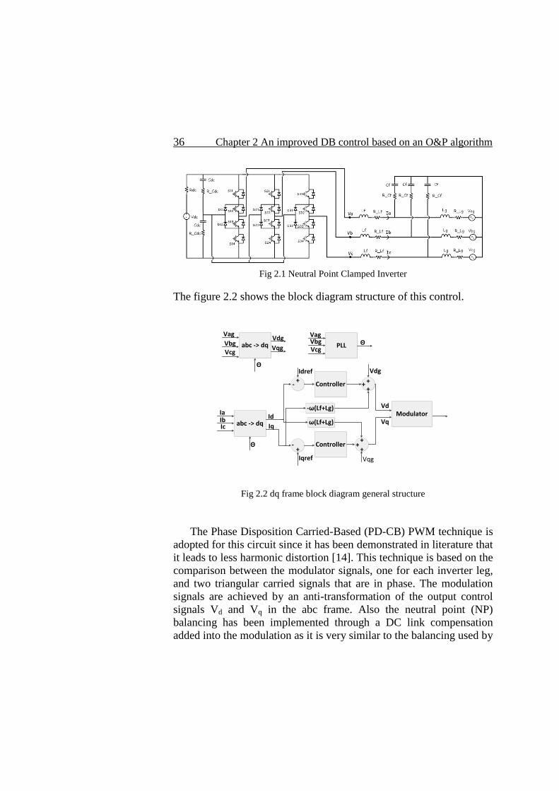
The figure 2.1 shows the analyzed system. As can be seen, it is a
three-level Neutral Point Diode Clamped Inverter described in the
chapter 1. The PV source can be connected to the NPC input directly
or, if it is necessary to adapt the PV voltage to the NPC input voltage,
by means a further conversion stage. It worth be noted that, for grid
connected inverters, the inductor Lg is usually not added as the grid
impedance is present. The problem is that this impedance is unknown
as it changes with the connection point to the grid. To take into
account this case, the inductor Lg is not considered in the control
techniques.
There are a lot of methodologies to control the output inverter
phase currents Ia, Ib and Ic. The most intuitive is to use a controller for
each phase current but it is possible to exploit the symmetrical
proprieties of the three-phase systems in order to reduce the number of
controllers from three to two as described in the chapter and so the
control is performed exploiting the Park Transform in the dq frame.
36 Chapter 2 An improved DB control based on an O&P algorithm
Fig 2.1 Neutral Point Clamped Inverter
The figure 2.2 shows the block diagram structure of this control.
abc -> dq
IaIbIc
Id
Iq
Idref
Iqref
Controller
Controller
-ω(Lf+Lg)
ω(Lf+Lg)
+-
+-
++
Vdg
+
++
Vqg
+
Modulator
PLL
VagVbgVcg
Θ
Θ
abc -> dq
Vag
VbgVcg
Vdg
Vqg
Θ
Vd
Vq
Fig 2.2 dq frame block diagram general structure
The Phase Disposition Carried-Based (PD-CB) PWM technique is
adopted for this circuit since it has been demonstrated in literature that
it leads to less harmonic distortion [14]. This technique is based on the
comparison between the modulator signals, one for each inverter leg,
and two triangular carried signals that are in phase. The modulation
signals are achieved by an anti-transformation of the output control
signals Vd and Vq in the abc frame. Also the neutral point (NP)
balancing has been implemented through a DC link compensation
added into the modulation as it is very similar to the balancing used by
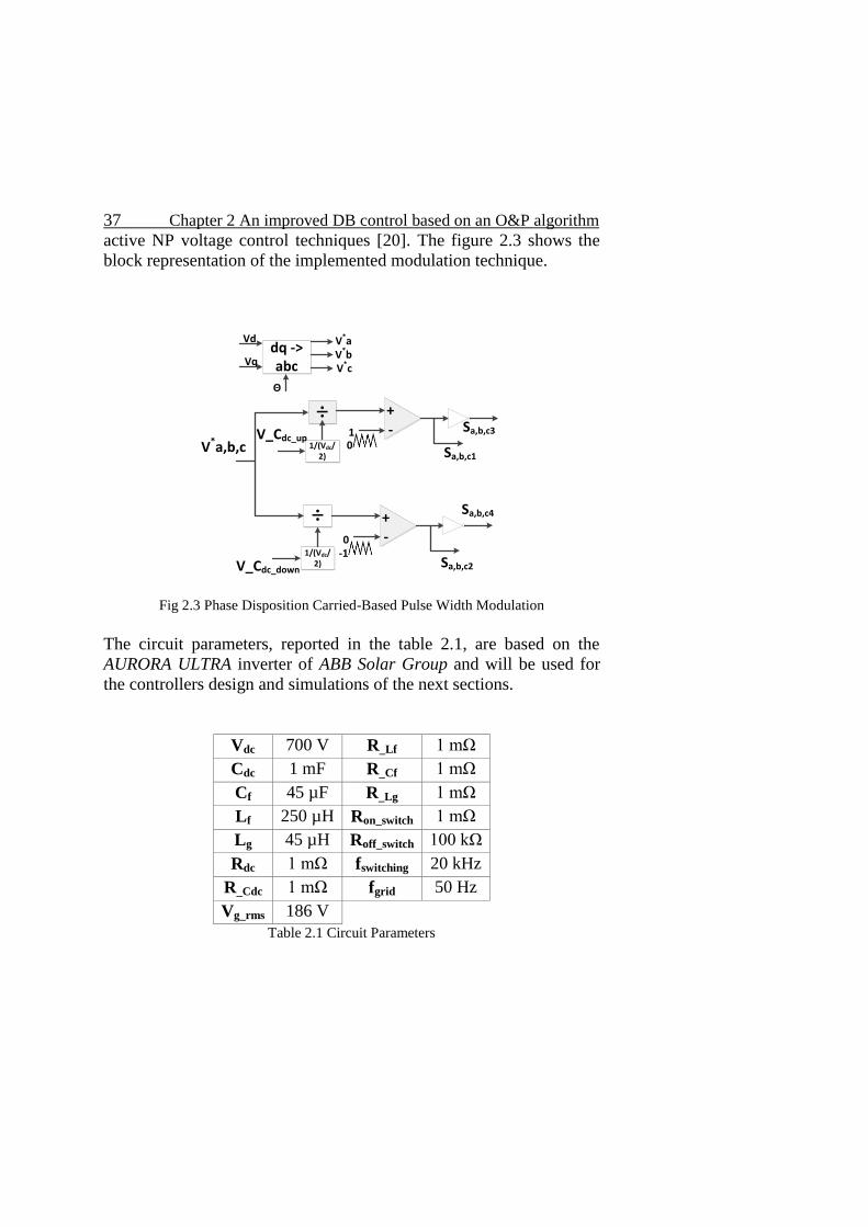
37 Chapter 2 An improved DB control based on an O&P algorithm
active NP voltage control techniques [20]. The figure 2.3 shows the
block representation of the implemented modulation technique.
V*a,b,c
÷ +-
1/(Vdc/2)
V_Cdc_up
÷ +-
1/(Vdc/2)V_Cdc_down
1
0-1
0Sa,b,c1
Sa,b,c2
Sa,b,c3
Sa,b,c4
dq -> abc
V*aV*bV*c
Θ
Vd
Vq
Fig 2.3 Phase Disposition Carried-Based Pulse Width Modulation
The circuit parameters, reported in the table 2.1, are based on the
AURORA ULTRA inverter of ABB Solar Group and will be used for
the controllers design and simulations of the next sections.
Vdc 700 V R_Lf 1 mΩ
Cdc 1 mF R_Cf 1 mΩ
Cf 45 µF R_Lg 1 mΩ
Lf 250 µH Ron_switch 1 mΩ
Lg 45 µH Roff_switch 100 kΩ
Rdc 1 mΩ fswitching 20 kHz
R_Cdc 1 mΩ fgrid 50 Hz
Vg_rms 186 V
Table 2.1 Circuit Parameters
38 Chapter 2 An improved DB control based on an O&P algorithm
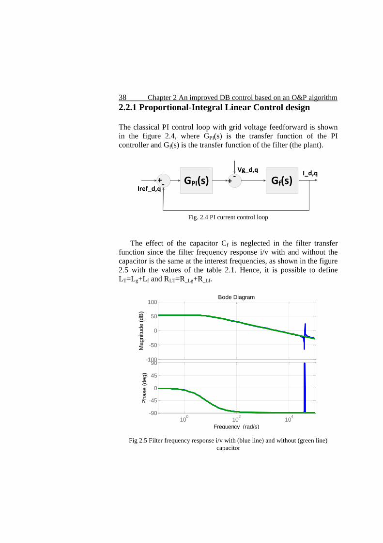
2.2.1 Proportional-Integral Linear Control design
The classical PI control loop with grid voltage feedforward is shown
in the figure 2.4, where GPI(s) is the transfer function of the PI
controller and Gf(s) is the transfer function of the filter (the plant).
Iref_d,qGPI(s)+-
-+
Vg_d,q
Gf(s)I_d,q
Fig. 2.4 PI current control loop
The effect of the capacitor Cf is neglected in the filter transfer
function since the filter frequency response i/v with and without the
capacitor is the same at the interest frequencies, as shown in the figure
2.5 with the values of the table 2.1. Hence, it is possible to define
LT=Lg+Lf and RLT=R_Lg+R_Lf.
-100
-50
0
50
100
Magnitude (
dB
)
100
102
104
-90
-45
0
45
90
Phase (
deg)
Bode Diagram
Frequency (rad/s)
Fig 2.5 Filter frequency response i/v with (blue line) and without (green line)
capacitor

39 Chapter 2 An improved DB control based on an O&P algorithm
The equations (2.7) and (2.8) show the transfer functions GPI(s) and
Gf(s).
1
( )f
T T
G sR sL
(2.7)
( ) IPI P
kG s k
s
(2.8)
To calculate kP and kI, a cross-over frequency fc equal to 700Hz and a
phase margin ϕm equal to 70° have been imposed to the open-loop
gain transfer function Gf(s)GPI(s), with the values of the table 2.1,
leading to the following values:
1.2
2000
P
I
k
k rad s
(2.9)
Typically, a digital device, such as a microcontroller or a DSP, is
used to implement this controller [26]. Hence, the transfer function
GPI(s) is discretized with the Tustin transform as shown in the
equations (2.10):
2 1
11
( ) ( )2 1
( ) (( 1) )( ) (( 1) )
2
( ) ( ) ( )
zs
I Tc zPI P PI P I
I I I
P I
k Tc zG s k G z k k
s z
e kTc e k Tcu kTc k Tc u k Tc
V kTc k e kTc u kTc
(2.10)
where e(kTc) = iref - i(kTc) is the tracking error at the instant kTc.
The sampling frequency has been chosen to 20kHz, typical value
used for this inverter by ABB Solar Group.
Also, coupled terms between the components d and q are also
present with the Park Transform, as shown in the chapter 1, equation
(1.5) and so decoupled compensation terms are added in the control
laws [14], [26], as shown in the figure 2.2.

40 Chapter 2 An improved DB control based on an O&P algorithm
Thus, taking into account the feedforward grid voltage
compensation and the decoupling term of the Park Transform, the
following control laws are implemented:
( ) (( 1) )( ) (( 1) )
2
( ) ( ) ( ) ( )
( ) (( 1) )( ) (( 1) )
2
( ) ( ) ( ) ( )
d ddI I dI
d P d dI dg T q
q q
qI I qI
q P q qI qg T d
e kTc e k Tcu kTc k Tc u k Tc
V kTc k e kTc u kTc V wL i kTc
e kTc e k Tcu kTc k Tc u k Tc
V kTc k e kTc u kTc V wL i kTc
(2.11)
2.2.2 Dead-Beat control design
The design of the DB control is carried out on the basis of the grid
filter mathematical model [14], [26] in term of dq transformation
where, as for the PI control, the capacitors Cf are neglected.
Looking at the figure 2.1 and defining LT=Lg+Lf and
RLT=R_Lg+R_Lf, it is possible to write [26]:
1 0 0 2 1 1 1 0 01 1
0 1 0 1 2 1 0 1 03
0 0 1 1 1 2 0 0 1
aga a a
LTb b b bg
T T T
c c c cg
VI I VRd
I I V Vdt L L L
I I V V
(2.12)
Considering the Park Transform of the system equations (2.12):
1 10 0
1 10 0
LT
gdd d dT T T
q q qLT gq
T TT
Rw
Vi i VL L Ld
i i VR Vdtw
L LL
(2.13)

41 Chapter 2 An improved DB control based on an O&P algorithm
and applying to the (2.13) the Forward Euler method [26]:
(( 1) ) ( )t kTc
di i k Tc i kTc
dt Tc
(2.14)
it is possible to calculate the discrete model at (k+1)-th instant:
1 0 0( )(( 1) ) ( ) ( )
(( 1) ( ) ( ) ( )0 01
LT
gdd d dT T T
q q qLT gq
T TT
TcR Tc TcTcw
V kTci k Tc i kTc V kTcL L L
i k Tc i kTc V kTcTcR Tc Tc V kTcTcw
L LL
(2.15)
The sampling frequency is set equal to 20kHz as for the PI control.
In principle, it is possible to set the currents id and iq equal to the
reference currents at the end of the sampling period, DB 1delay,
neglecting the computation delay [26]:
(( 1) ) ( )
(( 1) )) ( )
d dref
q qref
i k Tc i kTc
i k Tc i kTc
(2.16)
The equations (2.16) make the DB control very fast as it is able to lead
id and iq equal to the reference currents in 1 sampling time.
Replacing the (2.16) into the (2.15) and defining the errors
ed(k)=idref(k) – id(k+1) and eq(k)=iqref(k) – iq(k+1), the control laws are
determined:
( ) ( ) ( ) ( ) ( )
( ) ( ) ( ) ( ) ( )
Td d LT d T q gd
Tq q LT q T d gq
LV kTc e Tck R i kTc L wi kTc V kTc
Tc
LV kTc e Tck R i kTc L wi kTc V kTc
Tc
(2.17)
As a real digital device needs a finite time to perform the calculations,
the currents id and iq have to be set equal to the reference currents at
the end of next sampling time, DB 2delay:
42 Chapter 2 An improved DB control based on an O&P algorithm
(( 2) ) ( )
(( 2) )) ( )
d dref
q qref
i k Tc i kTc
i k Tc i kTc
(2.18)
but the DB control keeps very fast as Tc<<Tgrid.
Writing the discrete model from the (2.13) for the (k+2)-th instant
with the Forward Euler method, replacing the (2.15) in the result and
neglecting the parasitic resistances RT as it is usually done [26], the
control laws, shown in the equations (2.19), can be written:
1 ( ) ( ) 1 ( ) 1
1 ( ) ( ) 1 ( ) 1
Td d d gd gd T q q
Tq q q gq gq T d d
LV k Tc e Tck V kTc V kTc V k Tc L w i kTc i k Tc
Tc
LV k Tc e Tck V kTc V kTc V k Tc L w i kTc i k Tc
Tc
(2.19)
Since the sampling frequency is much greater than the grid frequency
(fc=20kHz >> fgrid=50Hz), it is possible to set:
1 ( )
1 ( )
1
1 ( )
gd gd
q q
gq gq
d d
V k Tc V kTc
i k Tc i kTc
V k Tc V kTc
i k Tc i kTc
(2.20)
Thus, replacing the (2.20) into the (2.19), the final control laws are
calculated:
1 ( ) 2 ( ) 2 ( )
1 ( ) 2 ( ) 2 ( )
Td d d gd T q
Tq q q gq T d
LV k Tc e kTc V kTc V kTc L wi kTc
Tc
LV k Tc e kTc V kTc V kTc L wi kTc
Tc
(2.21)
It worth be noted that as all the control laws (2.17), (2.19) and (2.21)
are strongly dependent by the model assumptions, the DB control is
not able to guarantee zero tracking errors.

43 Chapter 2 An improved DB control based on an O&P algorithm
The Dead-Beat stability analysis [14], [26] can be done starting
from the (2.15) that can be written as:
(( 1) ) ( ) ( ) ( ) ( )
(( 1) ) ( ) ( ) ( ) ( )
d d d gd q
q q q gq d
i k Tc ai kTc b V kTc V kTc ci kTc
i k Tc ai kTc b V kTc V kTc ci kTc
(2.22)
where
1 LT
T
T
TcRa
L
Tcb
L
c Tcw
Looking at the (2.22), it is possible to note the cross-coupling term ±c
due to the Park Transform as described in the chapter 1, equation
(1.5). As shown in the figure 2.2, like for the PI control, decoupled
compensation terms [14], [26] have been introduced that are the terms
±LTω in the (2.17) and ±2LTω in the (2.21) making the (2.22)
decoupled equations. Hence, it is possible to write:
(( 1) ) ( ) ( ) ( )d d d gdi k Tc ai kTc b V kTc V kTc
(2.23)
Where only the d component is considered as the same results can be
found for the q component.
Applying the Z-transform to the equation (2.23):
( ) ( ) ( )d dzI z aI z bU z
(2.24)
where
( ) ( ) ( )d gdu k V kTc V kTc
the plant transfer function is:

44 Chapter 2 An improved DB control based on an O&P algorithm
1
1
( )( )
( ) 1
df
I z bzG z
U z az
(2.25)
That is stable having 1 pole in a=(1-TcRLT/LT)<1.
In the design of the DB control, it has been set that the current is
equal to the reference current at the end of 1 or 2 sampling periods, as
shown in the equations (2.16) and (2.18). Hence the closed-loop
transfer function can be found applying the Z-Transform to the (2.18):
2
1( )CLG z
z
(2.26)
with k=1 or 2 and the DB transfer function becomes:
2 1
2 1
1 1 1( )
( ) 1DB
f
z azG z
G z z b z z
(2.27)
The equation (2.26) has 2 poles in the origin and so the closed-loop
system is stable.
As for the tracking errors d and q, also the stability is affect by the
model mismatch but the robustness of the DB control is very high [9],
[26]. Considering a mismatch of the inductor LT= LT±ΔLT, i.e.
replacing this value only in the (2.25) and calculating the poles using
also the (2.27), the poles of the closed loop systems are [9]:
1,2T
T
Lp
L
(2.28)
The equation (2.28) shows that unless there is a model mismatch of
100%LT, the system remains stable.
Hence, the model mismatch affects principally the state-state
errors d and q.

45 Chapter 2 An improved DB control based on an O&P algorithm
2.2.3 Hybrid solution: Dead-Beat and integral action
As described in the previous section, the DB control has a very fast
dynamic but presents a steady-state tracking error of a no zero value.
A first way to try to achieve that keeping the advantage of a fast
dynamic is a hybrid solution with an integral action that guarantee the
zero tracking error in steady-state condition: an Integral+DB (I+DB)
control. The integral action does not have to affect the dynamic of the
DB, i.e. ki values more and more close to the (2.9) lead to system
dynamic more and more similar to the PI dynamic, not justifying the
use of the DB control anymore. But, decreasing ki, the integral action
is not able to lead the average tracking error rapidly to zero.
Considering a trade-off between these two requirements, ki has been
set to 1/20 of the (2.9) and so ki=2000/20rad/s=100rad/s. This is the
limit of this solution: the average tracking error can be lower than the
DB but not yet zero as for the PI control because to keep the fast
dynamic of the DB, the integral action should be very slow, as it will
be shown with the simulation results.
2.3 Observe&Perturb Dead-Beat control
The proposed method is based on the MPPT Perturb&Observe
algorithm [24]. Since this algorithm first observes and then makes a
perturbation is called Observe&Perturb (O&P).
The goal of this control is to achieve a zero tracking error in
steady-state condition without affecting the dynamic response of the
standard DB control described in the previous section.
As the P&O [24], perturbations, ΔVd and ΔVq, are introduced by
the controller at fixed time step Ta in the control laws (2.17) and
(2.21) determining the equations (2.28), O&P DB 1delay, and (2.29),
O&P DB 2delay:
(( 1) ) ( ) ( ) ( ) ( )
(( 1) ) ( ) ( ) ( ) ( )
Td d LT d T q gd d
Tq q LT q T d gq q
LV n Ta e nTa R i nTa L wi nTa V nTa V
Tc
LV n Ta e nTa R i nTa L wi nTa V nTa V
Tc
(2.28)
46 Chapter 2 An improved DB control based on an O&P algorithm
( 1) ( ) 2 ( ) 2 ( )
( 1) ( ) 2 ( ) 2 ( )
Td d d gd T q d
Tq q q gq T d q
LV n Ta e nTa V nTa V nTa L wi nTa Vt
Tc
LV n Ta e nTa V nTa V nTa L wi nTa Vt
Tc
(2.29)
Hence the controller, for k≠nTa uses the (2.17) and (2.21) and for
k=nTa, the (2.28) and (2.29). It worth be noted that the DB 1delay,
equations (2.17) and (2.28), is considered as theoretical case study.
As in the [27] Ta was related to the settling time of the step
response, Ta for the O&P is set in order to do not affect the stability of
the system, i.e. the system needs to reach the next steady state point
before to have a new perturbation. In this way, these perturbations do
not have to be considered in the loop as they are an optimization of the
operating point, as for the P&O [23].
For the DB control, looking at the equations (2.16) and (2.18), the
new steady state is reached after 1 or 2 sampling periods [14] and so:
2Ta Tc
(2.30)
indicating with Tc the sampling period. To have some margin on this
condition, Ta has been chosen equal to 5(2Tc)=500µs.
The perturbations, ΔVd and ΔVq, are calculated on the basis of the
average errors of the component d and q that is runtime calculated at
the fixed time Ta:
1_
( )N
d
kd mean
e k
EN
(2.31)
1_
( )N
q
kq mean
e k
EN
(2.32)
where N=Ta/Tc=10.
47 Chapter 2 An improved DB control based on an O&P algorithm
The bigger the average errors, the bigger has to be the
perturbations magnitude while the perturbations sign is the same of
the average error sign. Hence ΔVd and ΔVq are increased or decreased
of values ΔΔVd and ΔΔVq that are much bigger when the relative
average error absolute value increases. The figure 2.6 shows the
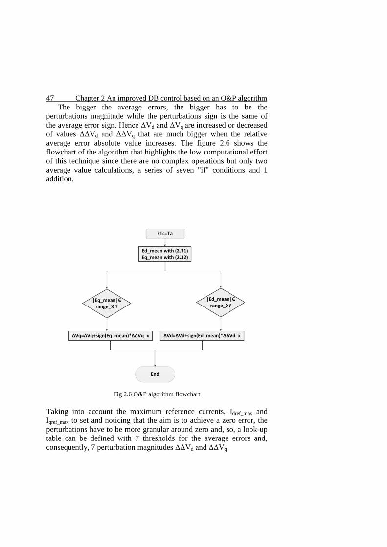
flowchart of the algorithm that highlights the low computational effort
of this technique since there are no complex operations but only two
average value calculations, a series of seven "if" conditions and 1
addition.
|Eq_mean|Є range_X ?
Ed_mean with (2.31)Eq_mean with (2.32)
kTc=Ta
ΔVq=ΔVq+sign(Eq_mean)*ΔΔVq_x
|Ed_mean|Є range_X?
ΔVd=ΔVd+sign(Ed_mean)*ΔΔVd_x
End
Fig 2.6 O&P algorithm flowchart
Taking into account the maximum reference currents, Idref_max and
Iqref_max to set and noticing that the aim is to achieve a zero error, the
perturbations have to be more granular around zero and, so, a look-up
table can be defined with 7 thresholds for the average errors and,
consequently, 7 perturbation magnitudes ΔΔVd and ΔΔVq.
48 Chapter 2 An improved DB control based on an O&P algorithm
The values for the average errors can be determined setting a
minimum and maximum percent errors, (Ed,q_mean/ Id,qref_max *100), that
are desired while for ΔΔVd and ΔΔVq the minimum and maximum
variation of Vd and Vq that corresponds to a minimum and maximum
variation of the voltages Va, Vb and Vc of the figure 2.1. Also the
maximum perturbation amplitudes, ΔVdmax and ΔVqmax have to be
much smaller of the Vdmax and Vqmax in order to do not affect the
dynamic and the stability of the system in the (2.28) and (2.29) [24].
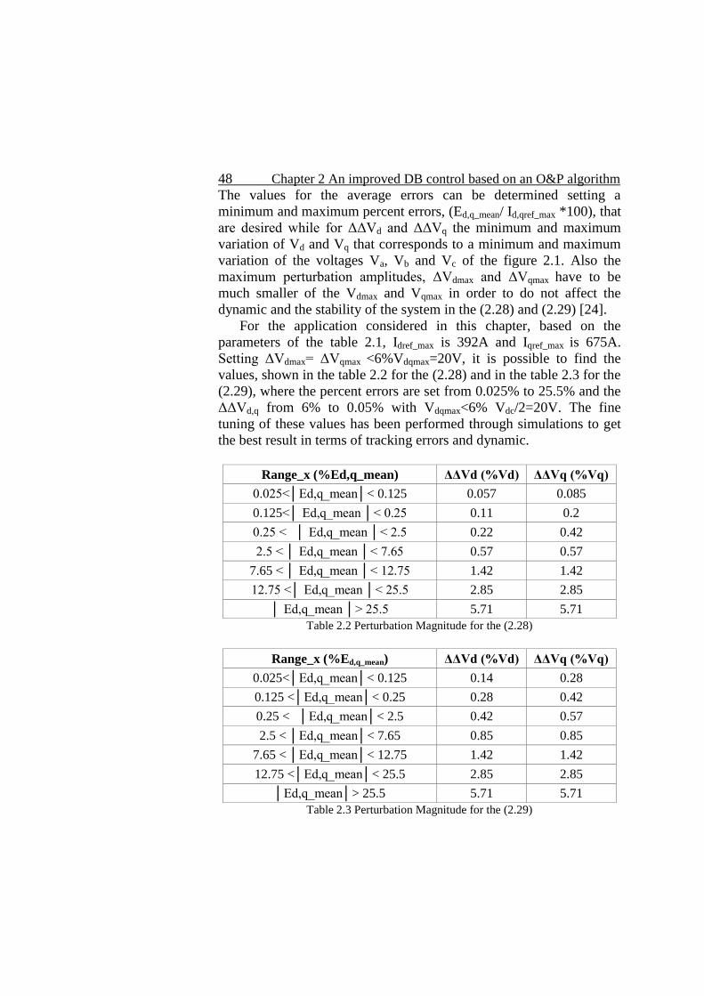
For the application considered in this chapter, based on the
parameters of the table 2.1, Idref_max is 392A and Iqref_max is 675A.
Setting ΔVdmax= ΔVqmax <6%Vdqmax=20V, it is possible to find the
values, shown in the table 2.2 for the (2.28) and in the table 2.3 for the
(2.29), where the percent errors are set from 0.025% to 25.5% and the
ΔΔVd,q from 6% to 0.05% with Vdqmax<6% Vdc/2=20V. The fine
tuning of these values has been performed through simulations to get
the best result in terms of tracking errors and dynamic.
Range_x (%Ed,q_mean) ΔΔVd (%Vd) ΔΔVq (%Vq)
0.025<│Ed,q_mean│< 0.125 0.057 0.085
0.125<│ Ed,q_mean │< 0.25 0.11 0.2
0.25 < │ Ed,q_mean │< 2.5 0.22 0.42
2.5 < │ Ed,q_mean │< 7.65 0.57 0.57
7.65 < │ Ed,q_mean │< 12.75 1.42 1.42
12.75 <│ Ed,q_mean │< 25.5 2.85 2.85
│ Ed,q_mean │> 25.5 5.71 5.71
Table 2.2 Perturbation Magnitude for the (2.28)
Range_x (%Ed,q_mean) ΔΔVd (%Vd) ΔΔVq (%Vq)
0.025<│Ed,q_mean│< 0.125 0.14 0.28
0.125 <│Ed,q_mean│< 0.25 0.28 0.42
0.25 < │Ed,q_mean│< 2.5 0.42 0.57
2.5 < │Ed,q_mean│< 7.65 0.85 0.85
7.65 < │Ed,q_mean│< 12.75 1.42 1.42
12.75 <│Ed,q_mean│< 25.5 2.85 2.85
│Ed,q_mean│> 25.5 5.71 5.71
Table 2.3 Perturbation Magnitude for the (2.29)
49 Chapter 2 An improved DB control based on an O&P algorithm
2.4 Simulation results
In this section, the simulation results are reported for the previously
designed controllers, O&P DB, I+DB and PI with the circuit
parameters of the table 2.1. The same conditions and assumptions are
considered as in this way the different results are caused only by the
different control techniques.
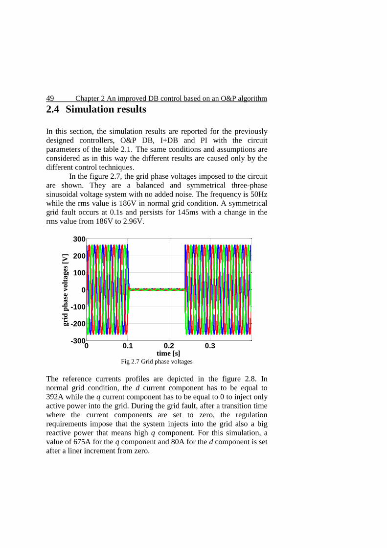
In the figure 2.7, the grid phase voltages imposed to the circuit
are shown. They are a balanced and symmetrical three-phase
sinusoidal voltage system with no added noise. The frequency is 50Hz
while the rms value is 186V in normal grid condition. A symmetrical
grid fault occurs at 0.1s and persists for 145ms with a change in the
rms value from 186V to 2.96V.
0 0.1 0.2 0.3-300
-200
-100
0
100
200
300
time [s]
gri
d p
hase
volt
ages
[V
]
Fig 2.7 Grid phase voltages
The reference currents profiles are depicted in the figure 2.8. In
normal grid condition, the d current component has to be equal to
392A while the q current component has to be equal to 0 to inject only
active power into the grid. During the grid fault, after a transition time
where the current components are set to zero, the regulation
requirements impose that the system injects into the grid also a big
reactive power that means high q component. For this simulation, a
value of 675A for the q component and 80A for the d component is set
after a liner increment from zero.
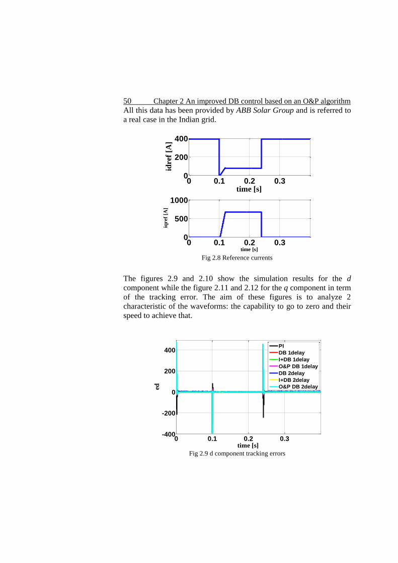
50 Chapter 2 An improved DB control based on an O&P algorithm
All this data has been provided by ABB Solar Group and is referred to
a real case in the Indian grid.
0 0.1 0.2 0.30
200
400
time [s]
id
ref
[A]
0 0.1 0.2 0.30
500
1000
time [s]
iq
ref
[A]
Fig 2.8 Reference currents
The figures 2.9 and 2.10 show the simulation results for the d
component while the figure 2.11 and 2.12 for the q component in term
of the tracking error. The aim of these figures is to analyze 2
characteristic of the waveforms: the capability to go to zero and their
speed to achieve that.
0 0.1 0.2 0.3-400
-200
0
200
400
time [s]
ed
PI
DB 1delay
I+DB 1delay
O&P DB 1delay
DB 2delay
I+DB 2delay
O&P DB 2delay
Fig 2.9 d component tracking errors
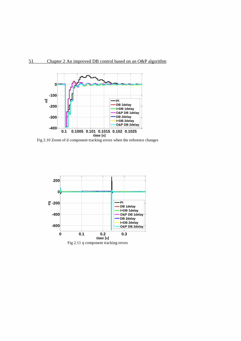
51 Chapter 2 An improved DB control based on an O&P algorithm
0.1 0.1005 0.101 0.1015 0.102 0.1025-400
-300
-200
-100
0
time [s]
ed
PI
DB 1delay
I+DB 1delay
O&P DB 1delay
DB 2delay
I+DB 2delay
O&P DB 2delay
Fig 2.10 Zoom of d component tracking errors when the reference changes
0 0.1 0.2 0.3
-600
-400
-200
0
200
time [s]
eq
PI
DB 1delay
I+DB 1delay
O&P DB 1delay
DB 2delay
I+DB 2delay
O&P DB 2delay
Fig 2.11 q component tracking errors
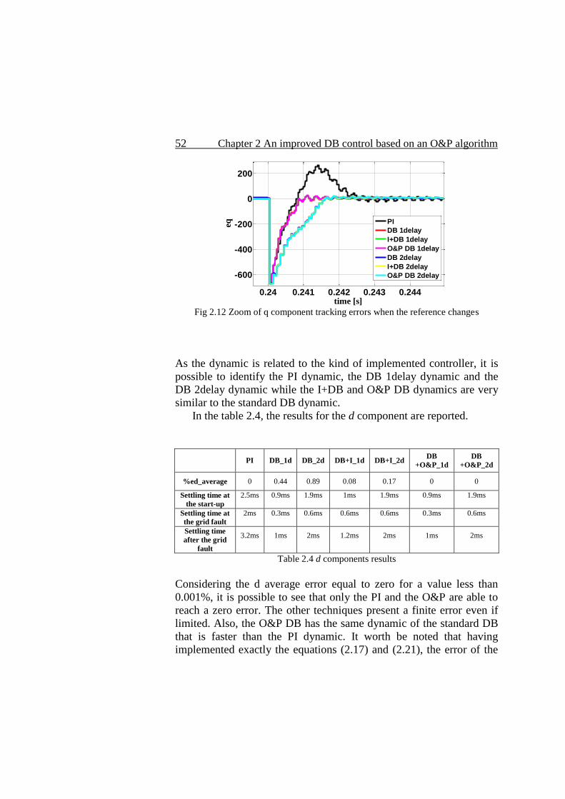
52 Chapter 2 An improved DB control based on an O&P algorithm
0.24 0.241 0.242 0.243 0.244
-600
-400
-200
0
200
time [s]
eq
PI
DB 1delay
I+DB 1delay
O&P DB 1delay
DB 2delay
I+DB 2delay
O&P DB 2delay
Fig 2.12 Zoom of q component tracking errors when the reference changes
As the dynamic is related to the kind of implemented controller, it is
possible to identify the PI dynamic, the DB 1delay dynamic and the
DB 2delay dynamic while the I+DB and O&P DB dynamics are very
similar to the standard DB dynamic.
In the table 2.4, the results for the d component are reported.
PI DB_1d DB_2d DB+I_1d DB+I_2d DB
+O&P_1d
DB
+O&P_2d
%ed_average 0 0.44 0.89 0.08 0.17 0 0
Settling time at
the start-up
2.5ms
0.9ms
1.9ms
1ms
1.9ms
0.9ms
1.9ms
Settling time at
the grid fault
2ms
0.3ms
0.6ms
0.6ms
0.6ms
0.3ms
0.6ms
Settling time
after the grid
fault
3.2ms
1ms
2ms
1.2ms
2ms
1ms
2ms
Table 2.4 d components results
Considering the d average error equal to zero for a value less than
0.001%, it is possible to see that only the PI and the O&P are able to
reach a zero error. The other techniques present a finite error even if
limited. Also, the O&P DB has the same dynamic of the standard DB
that is faster than the PI dynamic. It worth be noted that having
implemented exactly the equations (2.17) and (2.21), the error of the
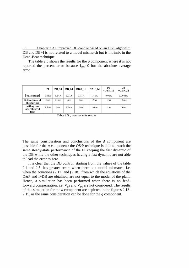
53 Chapter 2 An improved DB control based on an O&P algorithm
DB and DB+I is not related to a model mismatch but is intrinsic in the
Dead-Beat technique.
The table 2.5 shows the results for the q component where it is not
reported the percent error because Iqref=0 but the absolute average
error.
PI DB_1d DB_2d DB+I_1d DB+I_2d DB
+O&P_1d
DB
+O&P_2d
│eq_average│ 0.01A 1.54A 3.07A 0.71A 1.41A 0.01A 0.0043A
Settling time at
the start-up
8ms
0.9ms 2ms
1ms
2ms
1ms
1.5ms
Settling time
after the grid
fault
2.5ms
1ms
1.6ms
1ms
1.6ms
1ms
1.6ms
Table 2.5 q components results
The same consideration and conclusions of the d component are
possible for the q component: the O&P technique is able to reach the
same steady-state performance of the PI keeping the fast dynamic of
the DB while the other techniques having a fast dynamic are not able
to lead the error to zero.
It is clear that the DB control, starting from the values of the table
2.4 and 2.5, has greater errors when there is a model mismatch, i.e.
when the equations (2.17) and (2.18), from which the equations of the
O&P and I+DB are obtained, are not equal to the model of the plant.
Hence, a simulation has been performed when there is no feed-
forward compensation, i.e. Vgd and Vgq are not considered. The results
of this simulation for the d component are depicted in the figures 2.13-
2.15, as the same consideration can be done for the q component.
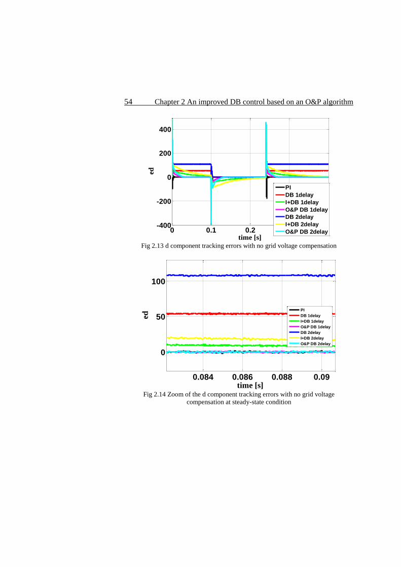
54 Chapter 2 An improved DB control based on an O&P algorithm
0 0.1 0.2 0.3-400
-200
0
200
400
time [s]
ed
PI
DB 1delay
I+DB 1delay
O&P DB 1delay
DB 2delay
I+DB 2delay
O&P DB 2delay
Fig 2.13 d component tracking errors with no grid voltage compensation
0.084 0.086 0.088 0.09
0
50
100
time [s]
ed
PI
DB 1delay
I+DB 1delay
O&P DB 1delay
DB 2delay
I+DB 2delay
O&P DB 2delay
Fig 2.14 Zoom of the d component tracking errors with no grid voltage
compensation at steady-state condition
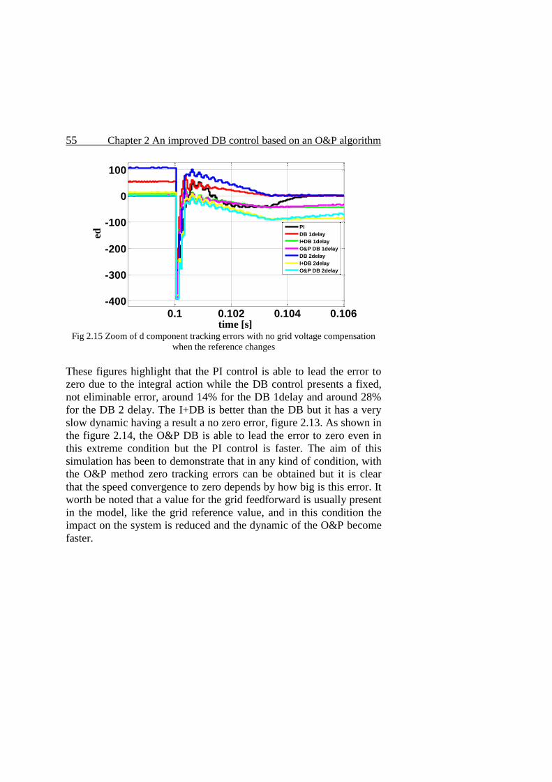
55 Chapter 2 An improved DB control based on an O&P algorithm
0.1 0.102 0.104 0.106-400
-300
-200
-100
0
100
time [s]
ed
PI
DB 1delay
I+DB 1delay
O&P DB 1delay
DB 2delay
I+DB 2delay
O&P DB 2delay
Fig 2.15 Zoom of d component tracking errors with no grid voltage compensation
when the reference changes
These figures highlight that the PI control is able to lead the error to
zero due to the integral action while the DB control presents a fixed,
not eliminable error, around 14% for the DB 1delay and around 28%
for the DB 2 delay. The I+DB is better than the DB but it has a very
slow dynamic having a result a no zero error, figure 2.13. As shown in
the figure 2.14, the O&P DB is able to lead the error to zero even in
this extreme condition but the PI control is faster. The aim of this
simulation has been to demonstrate that in any kind of condition, with
the O&P method zero tracking errors can be obtained but it is clear
that the speed convergence to zero depends by how big is this error. It
worth be noted that a value for the grid feedforward is usually present
in the model, like the grid reference value, and in this condition the
impact on the system is reduced and the dynamic of the O&P become
faster.
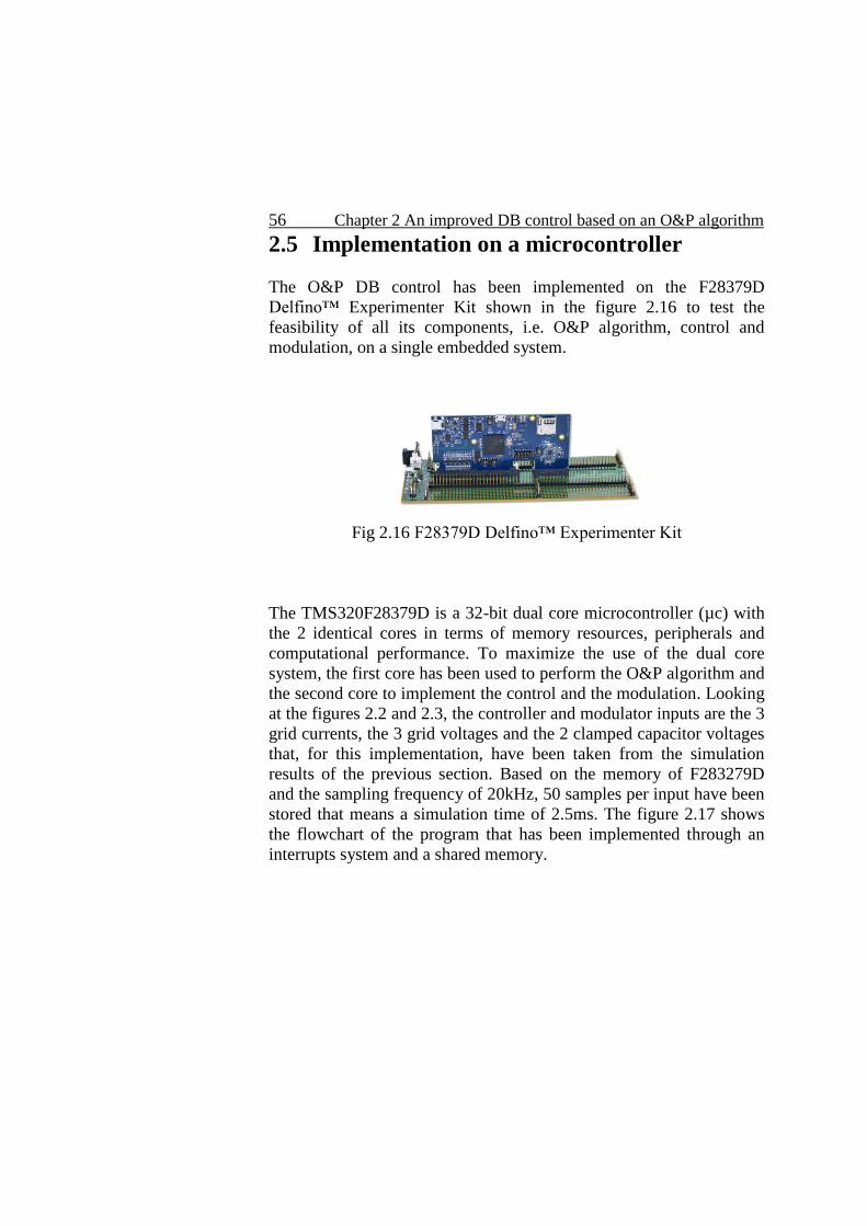
56 Chapter 2 An improved DB control based on an O&P algorithm
2.5 Implementation on a microcontroller
The O&P DB control has been implemented on the F28379D
Delfino™ Experimenter Kit shown in the figure 2.16 to test the
feasibility of all its components, i.e. O&P algorithm, control and
modulation, on a single embedded system.
Fig 2.16 F28379D Delfino™ Experimenter Kit
The TMS320F28379D is a 32-bit dual core microcontroller (µc) with
the 2 identical cores in terms of memory resources, peripherals and
computational performance. To maximize the use of the dual core
system, the first core has been used to perform the O&P algorithm and
the second core to implement the control and the modulation. Looking
at the figures 2.2 and 2.3, the controller and modulator inputs are the 3
grid currents, the 3 grid voltages and the 2 clamped capacitor voltages
that, for this implementation, have been taken from the simulation
results of the previous section. Based on the memory of F283279D
and the sampling frequency of 20kHz, 50 samples per input have been
stored that means a simulation time of 2.5ms. The figure 2.17 shows
the flowchart of the program that has been implemented through an
interrupts system and a shared memory.
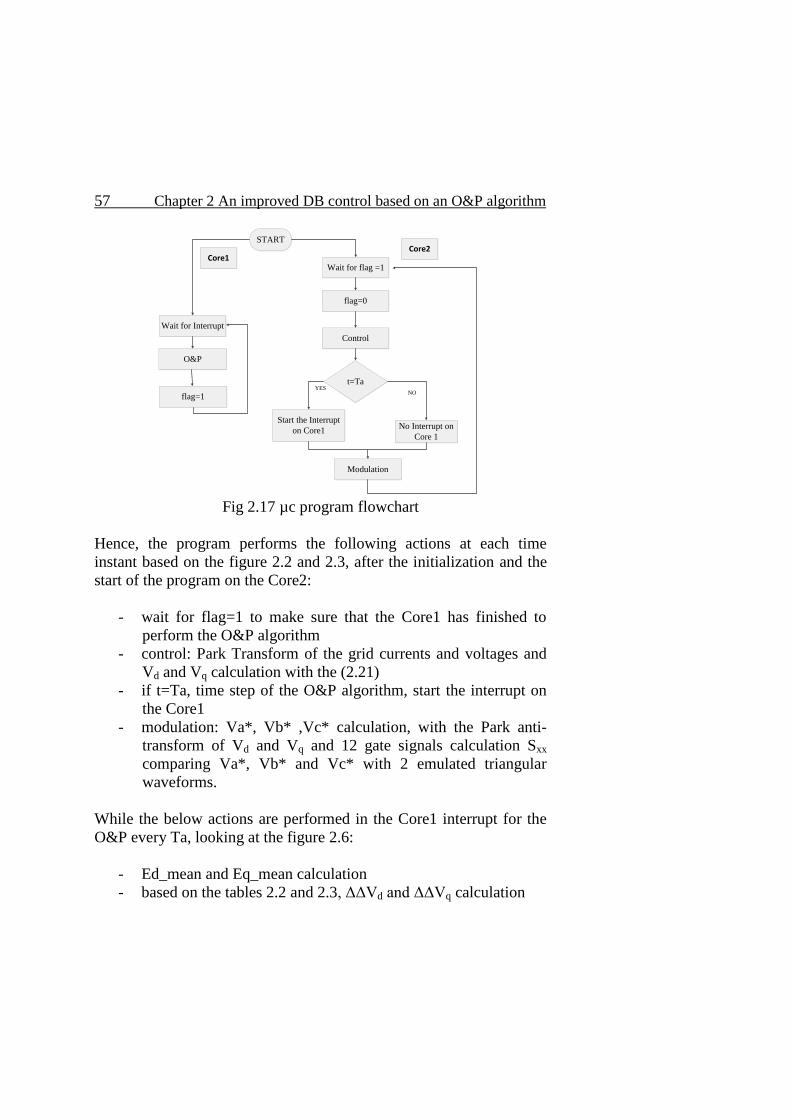
57 Chapter 2 An improved DB control based on an O&P algorithm
Wait for Interrupt
O&P
START
YES
flag=1
Control
t=Ta
No Interrupt on
Core 1
Wait for flag =1
Start the Interrupt
on Core1
Modulation
NO
Core1Core2
flag=0
Fig 2.17 µc program flowchart
Hence, the program performs the following actions at each time
instant based on the figure 2.2 and 2.3, after the initialization and the
start of the program on the Core2:
- wait for flag=1 to make sure that the Core1 has finished to
perform the O&P algorithm
- control: Park Transform of the grid currents and voltages and
Vd and Vq calculation with the (2.21)
- if t=Ta, time step of the O&P algorithm, start the interrupt on
the Core1
- modulation: Va*, Vb* ,Vc* calculation, with the Park anti-
transform of Vd and Vq and 12 gate signals calculation Sxx
comparing Va*, Vb* and Vc* with 2 emulated triangular
waveforms.
While the below actions are performed in the Core1 interrupt for the
O&P every Ta, looking at the figure 2.6:
- Ed_mean and Eq_mean calculation
- based on the tables 2.2 and 2.3, ΔΔVd and ΔΔVq calculation
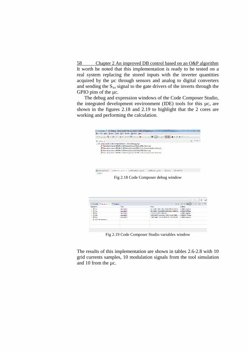
58 Chapter 2 An improved DB control based on an O&P algorithm
It worth be noted that this implementation is ready to be tested on a
real system replacing the stored inputs with the inverter quantities
acquired by the µc through sensors and analog to digital converters
and sending the Sxx signal to the gate drivers of the inverts through the
GPIO pins of the µc.
The debug and expression windows of the Code Composer Studio,
the integrated development environment (IDE) tools for this µc, are
shown in the figures 2.18 and 2.19 to highlight that the 2 cores are
working and performing the calculation.
Fig 2.18 Code Composer debug window
Fig 2.19 Code Composer Studio variables window
The results of this implementation are shown in tables 2.6-2.8 with 10
grid currents samples, 10 modulation signals from the tool simulation
and 10 from the µc.
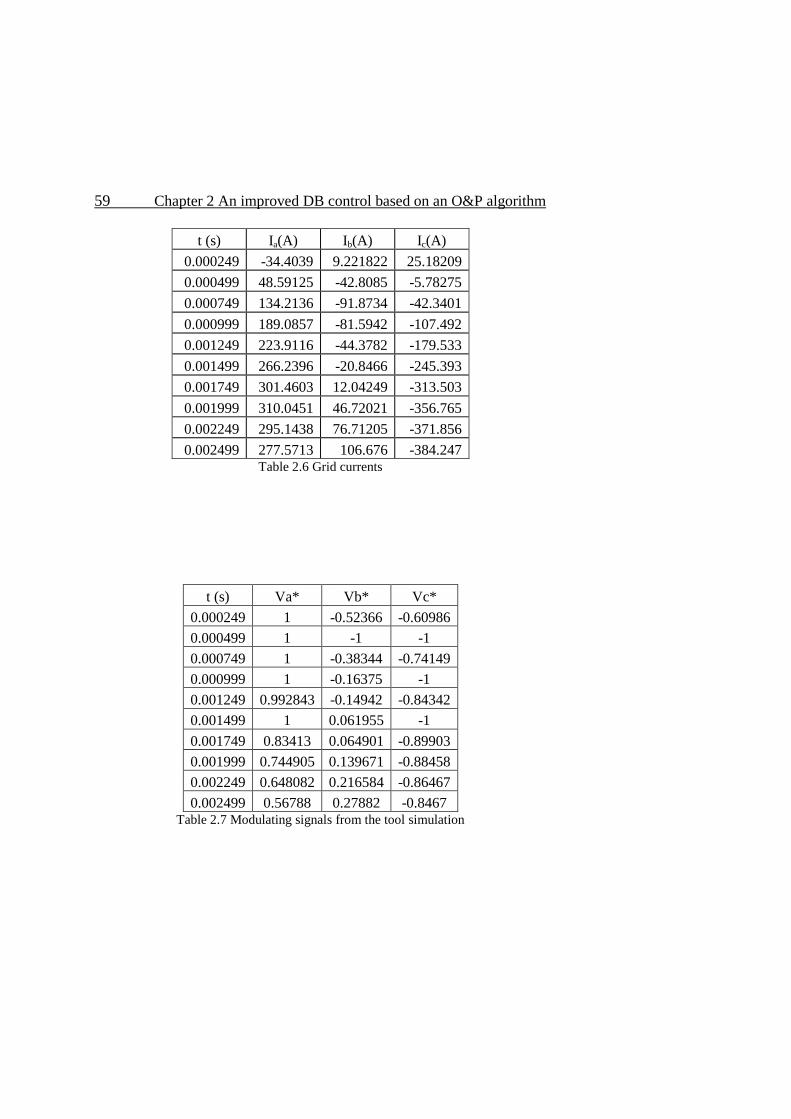
59 Chapter 2 An improved DB control based on an O&P algorithm
t (s) Ia(A) Ib(A) Ic(A)
0.000249 -34.4039 9.221822 25.18209
0.000499 48.59125 -42.8085 -5.78275
0.000749 134.2136 -91.8734 -42.3401
0.000999 189.0857 -81.5942 -107.492
0.001249 223.9116 -44.3782 -179.533
0.001499 266.2396 -20.8466 -245.393
0.001749 301.4603 12.04249 -313.503
0.001999 310.0451 46.72021 -356.765
0.002249 295.1438 76.71205 -371.856
0.002499 277.5713 106.676 -384.247 Table 2.6 Grid currents
t (s) Va* Vb* Vc*
0.000249 1 -0.52366 -0.60986
0.000499 1 -1 -1
0.000749 1 -0.38344 -0.74149
0.000999 1 -0.16375 -1
0.001249 0.992843 -0.14942 -0.84342
0.001499 1 0.061955 -1
0.001749 0.83413 0.064901 -0.89903
0.001999 0.744905 0.139671 -0.88458
0.002249 0.648082 0.216584 -0.86467
0.002499 0.56788 0.27882 -0.8467 Table 2.7 Modulating signals from the tool simulation
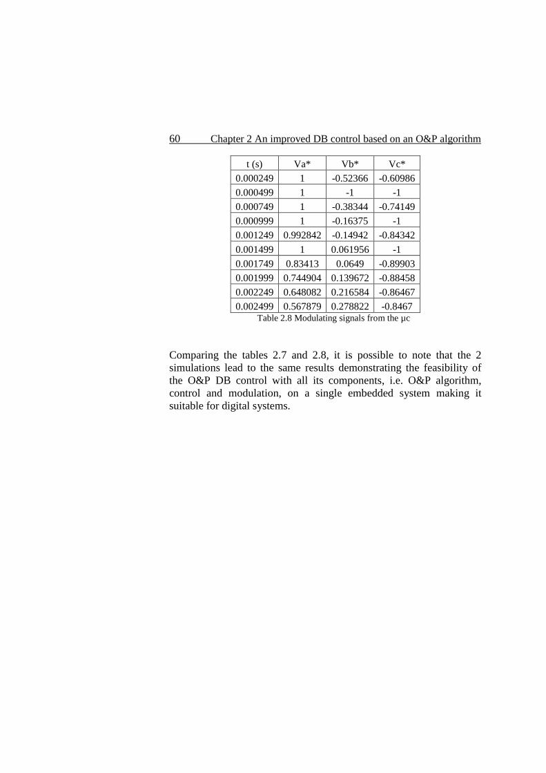
60 Chapter 2 An improved DB control based on an O&P algorithm
t (s) Va* Vb* Vc*
0.000249 1 -0.52366 -0.60986
0.000499 1 -1 -1
0.000749 1 -0.38344 -0.74149
0.000999 1 -0.16375 -1
0.001249 0.992842 -0.14942 -0.84342
0.001499 1 0.061956 -1
0.001749 0.83413 0.0649 -0.89903
0.001999 0.744904 0.139672 -0.88458
0.002249 0.648082 0.216584 -0.86467
0.002499 0.567879 0.278822 -0.8467 Table 2.8 Modulating signals from the µc
Comparing the tables 2.7 and 2.8, it is possible to note that the 2
simulations lead to the same results demonstrating the feasibility of
the O&P DB control with all its components, i.e. O&P algorithm,
control and modulation, on a single embedded system making it
suitable for digital systems.
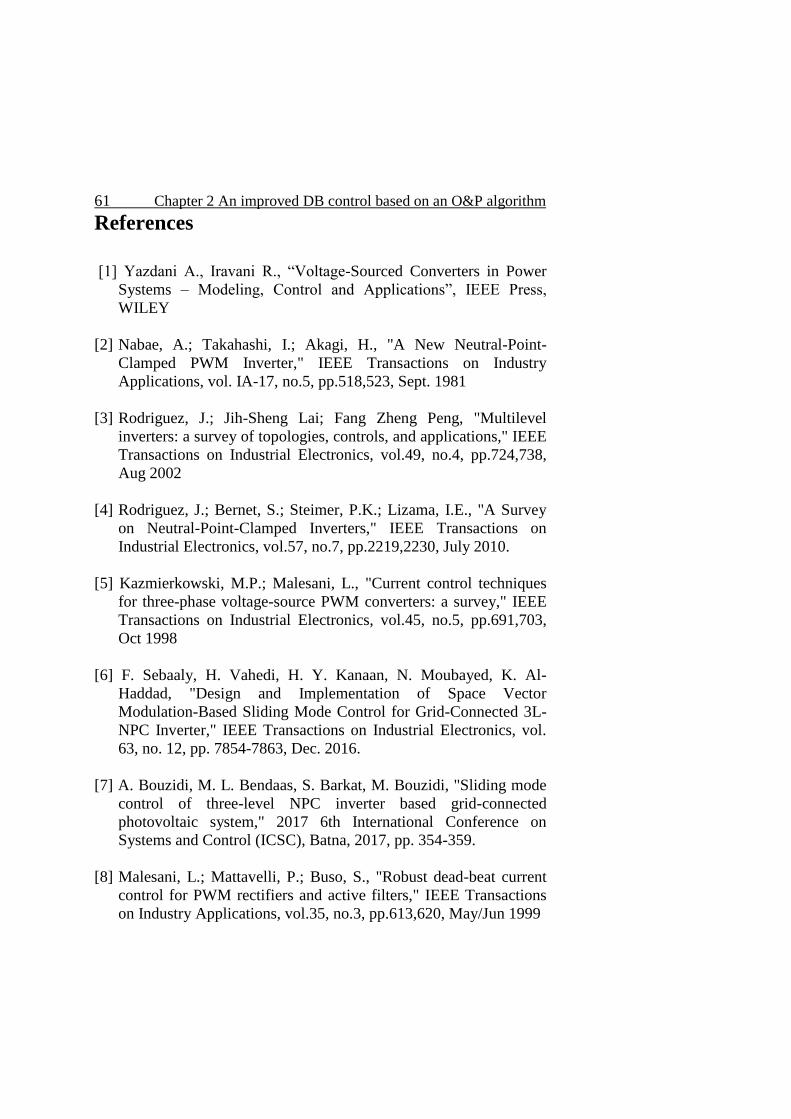
61 Chapter 2 An improved DB control based on an O&P algorithm
References
[1] Yazdani A., Iravani R., “Voltage-Sourced Converters in Power
Systems – Modeling, Control and Applications”, IEEE Press,
WILEY
[2] Nabae, A.; Takahashi, I.; Akagi, H., "A New Neutral-Point-
Clamped PWM Inverter," IEEE Transactions on Industry
Applications, vol. IA-17, no.5, pp.518,523, Sept. 1981
[3] Rodriguez, J.; Jih-Sheng Lai; Fang Zheng Peng, "Multilevel
inverters: a survey of topologies, controls, and applications," IEEE
Transactions on Industrial Electronics, vol.49, no.4, pp.724,738,
Aug 2002
[4] Rodriguez, J.; Bernet, S.; Steimer, P.K.; Lizama, I.E., "A Survey
on Neutral-Point-Clamped Inverters," IEEE Transactions on
Industrial Electronics, vol.57, no.7, pp.2219,2230, July 2010.
[5] Kazmierkowski, M.P.; Malesani, L., "Current control techniques
for three-phase voltage-source PWM converters: a survey," IEEE
Transactions on Industrial Electronics, vol.45, no.5, pp.691,703,
Oct 1998
[6] F. Sebaaly, H. Vahedi, H. Y. Kanaan, N. Moubayed, K. Al-
Haddad, "Design and Implementation of Space Vector
Modulation-Based Sliding Mode Control for Grid-Connected 3L-
NPC Inverter," IEEE Transactions on Industrial Electronics, vol.
63, no. 12, pp. 7854-7863, Dec. 2016.
[7] A. Bouzidi, M. L. Bendaas, S. Barkat, M. Bouzidi, "Sliding mode
control of three-level NPC inverter based grid-connected
photovoltaic system," 2017 6th International Conference on
Systems and Control (ICSC), Batna, 2017, pp. 354-359.
[8] Malesani, L.; Mattavelli, P.; Buso, S., "Robust dead-beat current
control for PWM rectifiers and active filters," IEEE Transactions
on Industry Applications, vol.35, no.3, pp.613,620, May/Jun 1999
62 Chapter 2 An improved DB control based on an O&P algorithm
[9] Rodriguez, J.; Pontt, J.; Silva, C.A.; Correa, P.; Lezana, P.; Cortes,
P.; Ammann, U., "Predictive Current Control of a Voltage Source
Inverter," IEEE Transactions on Industrial Electronics, vol.54,
no.1, pp.495,503, Feb. 2007
[10] Vargas, R.; Cortes, P.; Ammann, U.; Rodriguez, J.; Pontt, J.,
"Predictive Control of a Three-Phase Neutral-Point-Clamped
Inverter," IEEE Transactions on Industrial Electronics, vol.54,
no.5, pp.2697,2705, Oct. 2007
[11] Rodriguez, J.; Pontt, J.; Cortes, P.; Vargas, R., "Predictive
Control of a Three-Phase Neutral Point Clamped Inverter," IEEE
36th Power Electronics Specialists Conference, 2005. PESC '05.,
pp.1364,1369, 16-16 June 2005
[12] Blaabjerg, F.; Teodorescu, R.; Liserre, M.; Timbus, A.V.,
"Overview of Control and Grid Synchronization for Distributed
Power Generation Systems," IEEE Transactions on Industrial
Electronics, vol.53, no.5, pp.1398, 1409, Oct. 2006
[13] Timbus, A.; Liserre, M.; Teodorescu, R.; Rodriguez, P.;
Blaabjerg, F., "Evaluation of Current Controllers for Distributed
Power Generation Systems," IEEE Transactions on Power
Electronics, vol.24, no.3, pp.654,664, March 2009
[14] Teodorescu R., Liserre M., Rodriguez P., “Grid Converters for
Photovoltaic and Wind Power System”, IEEE Press, WILEY
[15] Holtz, J., "Pulsewidth modulation-a survey," IEEE Transactions
on Industrial Electronics, vol.39, no.5, pp.410,420, Oct 1992
[16] Holmes D., Lipo T., “Pulse Width Modulation For Power
Converters - Principles and Practice”, IEEE Press, WILEY-
INTERSCIENCE
[17] Kouro, S.; Lezana, P.; Angulo, Mauricio; Rodriguez, J.,
"Multicarrier PWM With DC-Link Ripple Feedforward
Compensation for Multilevel Inverters," IEEE Transactions on
Power Electronics, vol.23, no.1, pp.52,59, Jan. 2008
63 Chapter 2 An improved DB control based on an O&P algorithm
[18] McGrath, B.P.; Holmes, D.G., "Multicarrier PWM strategies for
multilevel inverters," IEEE Transactions on Industrial Electronics,
vol.49, no.4, pp.858, 867, Aug 2002
[19] Mohzani, Z.; McGrath, B.P.; Holmes, D.G., "The balancing
properties of DC link compensation for 3-phase Neutral Point
Clamped (NPC) Converter," 2012 7th International Power
Electronics and Motion Control Conference (IPEMC), vol.1,
pp.574,579, 2-5 June 2012
[20] du Toit Mouton, H., "Natural balancing of three-level neutral-
point-clamped PWM inverters," IEEE Transactions on Industrial
Electronics, vol.49, no.5, pp.1017,1025, Oct 2002
[21] Celanovic, N.; Boroyevich, D., "A comprehensive study of
neutral-point voltage balancing problem in three-level neutral-
point-clamped voltage source PWM inverters," IEEE Transactions
on Power Electronics, vol.15, no.2, pp.242,249, Mar 2000
[22] Holmes, Lipo, “Pulse Width Modulation for Power Converters -
Principles and Practice”, IEEE Press.
[23] N. Femia, G. Petrone, G. Spagnuolo, M. Vitelli, Power
Electronics and Control Techniques for Maximum Energy
Harvesting in Photovoltaic Systems, CRC press, 2012.
[24] Chua-Lin, “Computer-Aided Analysis of Electronic Circuits –
Algorithms and Computational Techniques”, Englewood Cliffs,
NJ: Prentice-Hall.
[25] N.Femia, "Understanding commutations in switching converters.
I. Basic theory and application of the Compensation Theorem,
"Transactions on Aerospace and Electronic Systems, IEEE vol.39,
no.1, pp.282, 297, Jan. 2003.
[26] S. Buso, P. Mattarelli, “Digital Control in Power Electronics”,
Morgan&Claypool Publishers

64 Chapter 2 An improved DB control based on an O&P algorithm
[27] N. Femia, G. Petrone, G. Spagnuolo, M. Vitelli, “Optimization of
Perturb and Observe Maximum Power Point Tracking Method”,
IEEE Transactions on Power Electronics, vol. 20, no. 4, pp. 963-
973, July 2005
Chapter 3
The Effect of a Constant Power Load
on the Stability of a Smart
Transformer
The high penetration of renewable energy source has led great
changes in the electric grid. The conventional grid was composed of a
source, a distribution energy system and loads. Instead, the new
scenario includes the presence of Distributed Power Generating
Systems (DPGSs) that can inject locally energy into the grid.
Moreover, the performances increase, combined with the costs
reduction of solid state devices, has led to the development and the
diffusion of the power converters with the result that, today, almost
the totality of the electrical energy is controlled by power electronic
systems.
The study of DPGSs is of a great interest from the point of view of
the overall system, where it is important to choice where it is
convenient to insert the DPGS [1], as well as from the point of view of
the local system where there are problems to control and
synchronization [2], [3]. A common way to find the optimal location
of DPGSs is to minimize the power losses of the system through
power flow algorithms as this is in general not sufficient. As the
DPGSs are based on renewable source, sun or wind for example, their
controllability is one of the main drawbacks. If these systems are not
well controlled, their connection to the grid can lead to instability or
failure. Besides, the capability of DPGSs to run under short grid
disturbances is stressful by the existing standard for interconnecting
these systems and so both synchronization algorithm and current
controller became very important.
The goal of this chapter is to investigate a scenario, shown in
figure 3.1, composed by a Smart Transformer (ST) [4], some loads
and some DPGSs directly connected to the low voltage side of the ST.
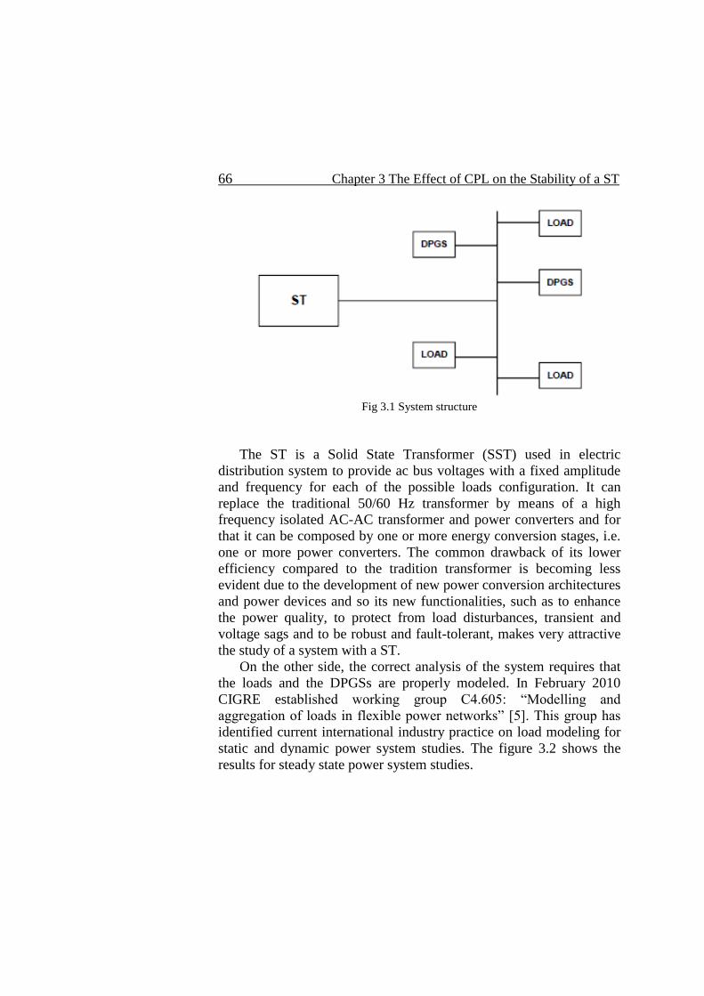
66 Chapter 3 The Effect of CPL on the Stability of a ST
Fig 3.1 System structure
The ST is a Solid State Transformer (SST) used in electric
distribution system to provide ac bus voltages with a fixed amplitude
and frequency for each of the possible loads configuration. It can
replace the traditional 50/60 Hz transformer by means of a high
frequency isolated AC-AC transformer and power converters and for
that it can be composed by one or more energy conversion stages, i.e.
one or more power converters. The common drawback of its lower
efficiency compared to the tradition transformer is becoming less
evident due to the development of new power conversion architectures
and power devices and so its new functionalities, such as to enhance
the power quality, to protect from load disturbances, transient and
voltage sags and to be robust and fault-tolerant, makes very attractive
the study of a system with a ST.
On the other side, the correct analysis of the system requires that
the loads and the DPGSs are properly modeled. In February 2010
CIGRE established working group C4.605: “Modelling and
aggregation of loads in flexible power networks” [5]. This group has
identified current international industry practice on load modeling for
static and dynamic power system studies. The figure 3.2 shows the
results for steady state power system studies.
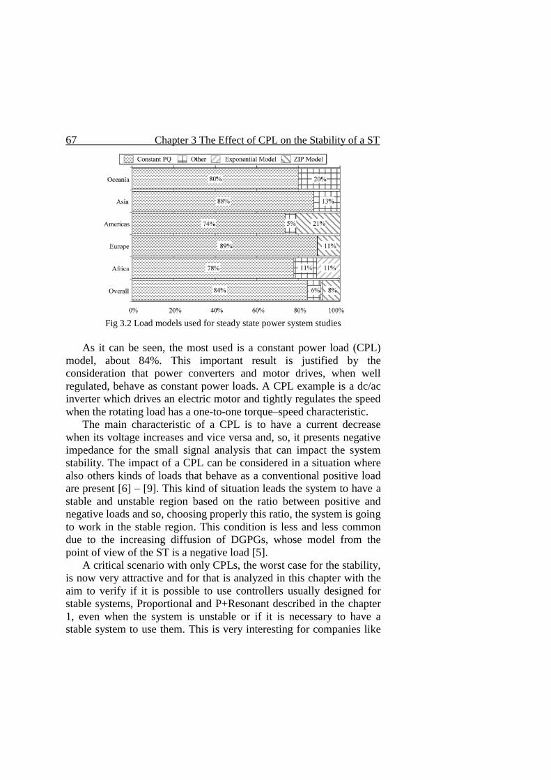
67 Chapter 3 The Effect of CPL on the Stability of a ST
Fig 3.2 Load models used for steady state power system studies
As it can be seen, the most used is a constant power load (CPL)
model, about 84%. This important result is justified by the
consideration that power converters and motor drives, when well
regulated, behave as constant power loads. A CPL example is a dc/ac
inverter which drives an electric motor and tightly regulates the speed
when the rotating load has a one-to-one torque–speed characteristic.
The main characteristic of a CPL is to have a current decrease
when its voltage increases and vice versa and, so, it presents negative
impedance for the small signal analysis that can impact the system
stability. The impact of a CPL can be considered in a situation where
also others kinds of loads that behave as a conventional positive load
are present [6] – [9]. This kind of situation leads the system to have a
stable and unstable region based on the ratio between positive and
negative loads and so, choosing properly this ratio, the system is going
to work in the stable region. This condition is less and less common
due to the increasing diffusion of DGPGs, whose model from the
point of view of the ST is a negative load [5].
A critical scenario with only CPLs, the worst case for the stability,
is now very attractive and for that is analyzed in this chapter with the
aim to verify if it is possible to use controllers usually designed for
stable systems, Proportional and P+Resonant described in the chapter
1, even when the system is unstable or if it is necessary to have a
stable system to use them. This is very interesting for companies like
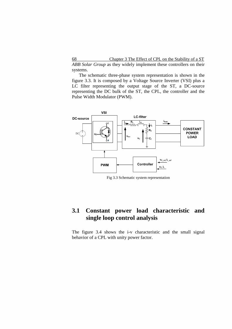
68 Chapter 3 The Effect of CPL on the Stability of a ST
ABB Solar Group as they widely implement these controllers on their
systems.
The schematic three-phase system representation is shown in the
figure 3.3. It is composed by a Voltage Source Inverter (VSI) plus a
LC filter representing the output stage of the ST, a DC-source
representing the DC bulk of the ST, the CPL, the controller and the
Pulse Width Modulator (PWM).
Fig 3.3 Schematic system representation
3.1 Constant power load characteristic and
single loop control analysis
The figure 3.4 shows the i-v characteristic and the small signal
behavior of a CPL with unity power factor.
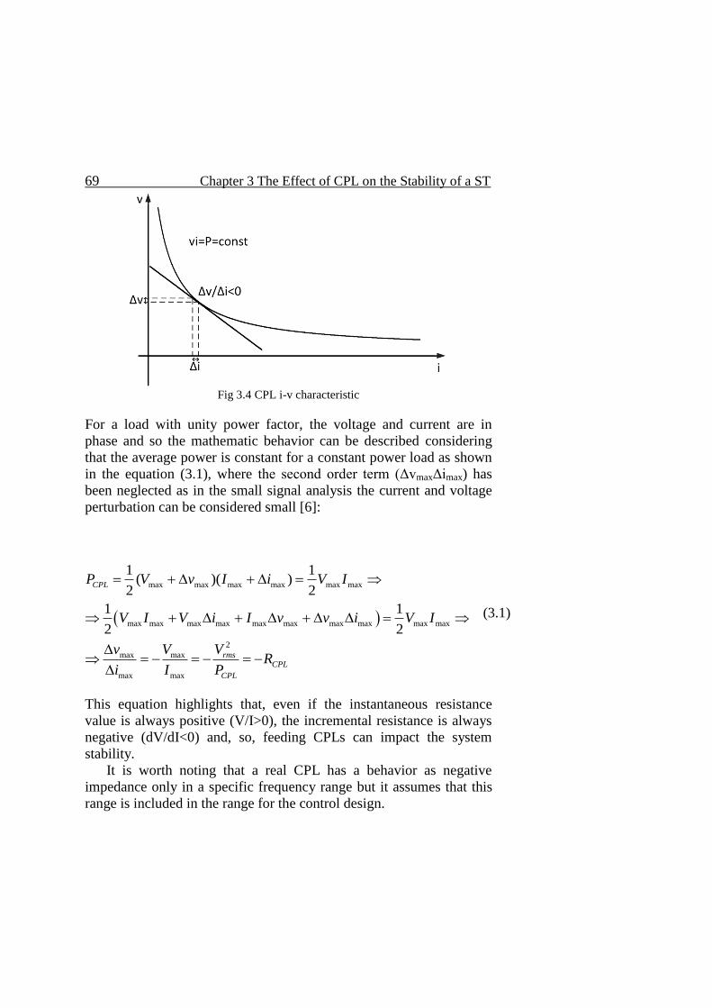
69 Chapter 3 The Effect of CPL on the Stability of a ST
Fig 3.4 CPL i-v characteristic
For a load with unity power factor, the voltage and current are in
phase and so the mathematic behavior can be described considering
that the average power is constant for a constant power load as shown
in the equation (3.1), where the second order term (ΔvmaxΔimax) has
been neglected as in the small signal analysis the current and voltage
perturbation can be considered small [6]:
max max max max max max
max max max max max max max max max max
2
max max
max max
1 1( )( )
2 2
1 1
2 2
CPL
rmsCPL
CPL
P V v I i V I
V I V i I v v i V I
v V VR
i I P
(3.1)
This equation highlights that, even if the instantaneous resistance
value is always positive (V/I>0), the incremental resistance is always
negative (dV/dI<0) and, so, feeding CPLs can impact the system
stability.
It is worth noting that a real CPL has a behavior as negative
impedance only in a specific frequency range but it assumes that this
range is included in the range for the control design.
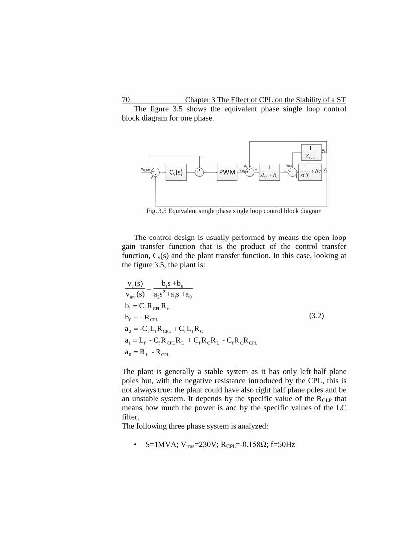
70 Chapter 3 The Effect of CPL on the Stability of a ST
The figure 3.5 shows the equivalent phase single loop control
block diagram for one phase.
Fig. 3.5 Equivalent single phase single loop control block diagram
The control design is usually performed by means the open loop
gain transfer function that is the product of the control transfer
function, Cv(s) and the plant transfer function. In this case, looking at
the figure 3.5, the plant is:
c 1 0
2
inv 2 1 0
1 f CPL c
0 CPL
2 f f CPL f f C
1 f f CPL L f C L f C CPL
0 L CPL
v (s) b s +b
v (s) a s +a s +a
b C R R
b - R
a -C L R C L R
a L - C R R + C R R - C R R
a R - R
(3.2)
The plant is generally a stable system as it has only left half plane
poles but, with the negative resistance introduced by the CPL, this is
not always true: the plant could have also right half plane poles and be
an unstable system. It depends by the specific value of the RCLP that
means how much the power is and by the specific values of the LC
filter.
The following three phase system is analyzed:
• S=1MVA; Vrms=230V; RCPL=-0.158Ω; f=50Hz
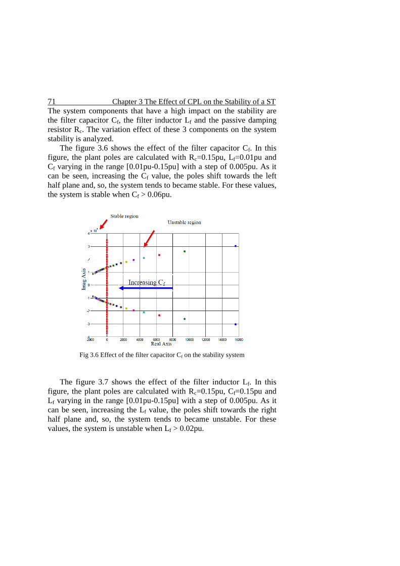
71 Chapter 3 The Effect of CPL on the Stability of a ST
The system components that have a high impact on the stability are
the filter capacitor Cf, the filter inductor Lf and the passive damping
resistor Rc. The variation effect of these 3 components on the system
stability is analyzed.
The figure 3.6 shows the effect of the filter capacitor Cf. In this
figure, the plant poles are calculated with Rc=0.15pu, Lf=0.01pu and
Cf varying in the range [0.01pu-0.15pu] with a step of 0.005pu. As it
can be seen, increasing the Cf value, the poles shift towards the left
half plane and, so, the system tends to became stable. For these values,
the system is stable when Cf > 0.06pu.
Fig 3.6 Effect of the filter capacitor Cf on the stability system
The figure 3.7 shows the effect of the filter inductor Lf. In this
figure, the plant poles are calculated with Rc=0.15pu, Cf=0.15pu and
Lf varying in the range [0.01pu-0.15pu] with a step of 0.005pu. As it
can be seen, increasing the Lf value, the poles shift towards the right
half plane and, so, the system tends to became unstable. For these
values, the system is unstable when Lf > 0.02pu.
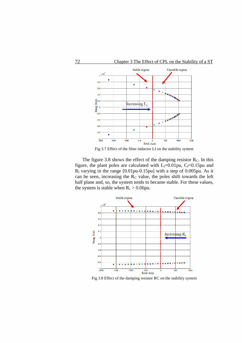
72 Chapter 3 The Effect of CPL on the Stability of a ST
Fig 3.7 Effect of the filter inductor Lf on the stability system
The figure 3.8 shows the effect of the damping resistor RC. In this
figure, the plant poles are calculated with Lf=0.01pu, Cf=0.15pu and
Rf varying in the range [0.01pu-0.15pu] with a step of 0.005pu. As it
can be seen, increasing the RC value, the poles shift towards the left
half plane and, so, the system tends to became stable. For these values,
the system is stable when Rc > 0.06pu.
Fig 3.8 Effect of the damping resistor RC on the stability system
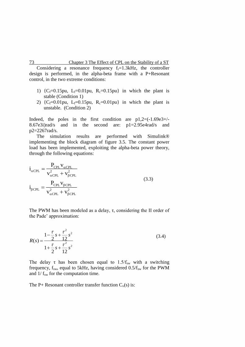
73 Chapter 3 The Effect of CPL on the Stability of a ST
Considering a resonance frequency fr=1.3kHz, the controller
design is performed, in the alpha-beta frame with a P+Resonant
control, in the two extreme conditions:
1) {Cf=0.15pu, Lf=0.01pu, Rc=0.15pu} in which the plant is
stable (Condition 1)
2) {Cf=0.01pu, Lf=0.15pu, Rc=0.01pu} in which the plant is
unstable. (Condition 2)
Indeed, the poles in the first condition are p1,2=(-1.69e3+/-
8.67e3i)rad/s and in the second are: p1=2.95e4rad/s and
p2=2267rad/s.
The simulation results are performed with Simulink®
implementing the block diagram of figure 3.5. The constant power
load has been implemented, exploiting the alpha-beta power theory,
through the following equations:
CPL CPLCPL 2 2
CPL CPL
CPL CPL
CPL 2 2
CPL CPL
P vi
v v
P vi
v v
(3.3)
The PWM has been modeled as a delay, τ, considering the II order of
the Pade’ approximation:
22
22
12 12( )
12 12
s sR s
s s
(3.4)
The delay τ has been chosen equal to 1.5/fsw with a switching
frequency, fsw, equal to 5kHz, having considered 0.5/fsw for the PWM
and 1/ fsw for the computation time.
The P+ Resonant controller transfer function Cv(s) is:
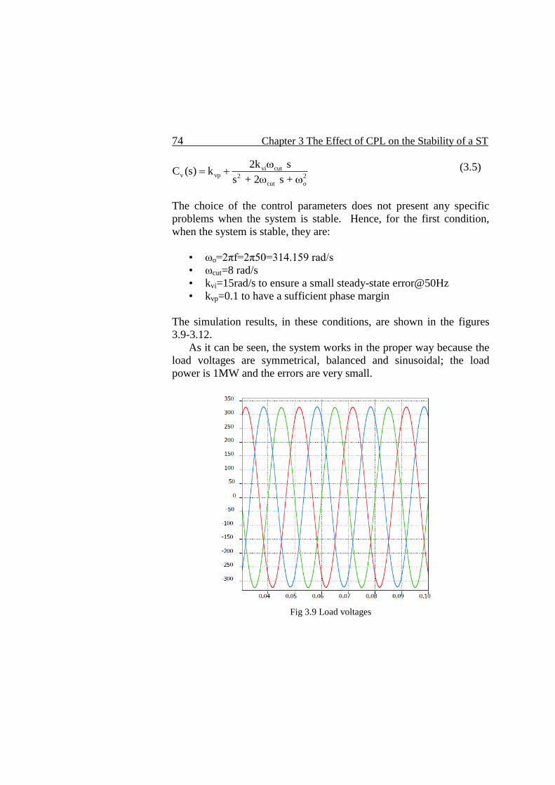
74 Chapter 3 The Effect of CPL on the Stability of a ST
vi cutv vp 2 2
cut o
2k sC (s) k
s + 2 s +
(3.5)
The choice of the control parameters does not present any specific
problems when the system is stable. Hence, for the first condition,
when the system is stable, they are:
• ωo=2πf=2π50=314.159 rad/s
• ωcut=8 rad/s
• kvi=15rad/s to ensure a small steady-state error@50Hz
• kvp=0.1 to have a sufficient phase margin
The simulation results, in these conditions, are shown in the figures
3.9-3.12.
As it can be seen, the system works in the proper way because the
load voltages are symmetrical, balanced and sinusoidal; the load
power is 1MW and the errors are very small.
Fig 3.9 Load voltages
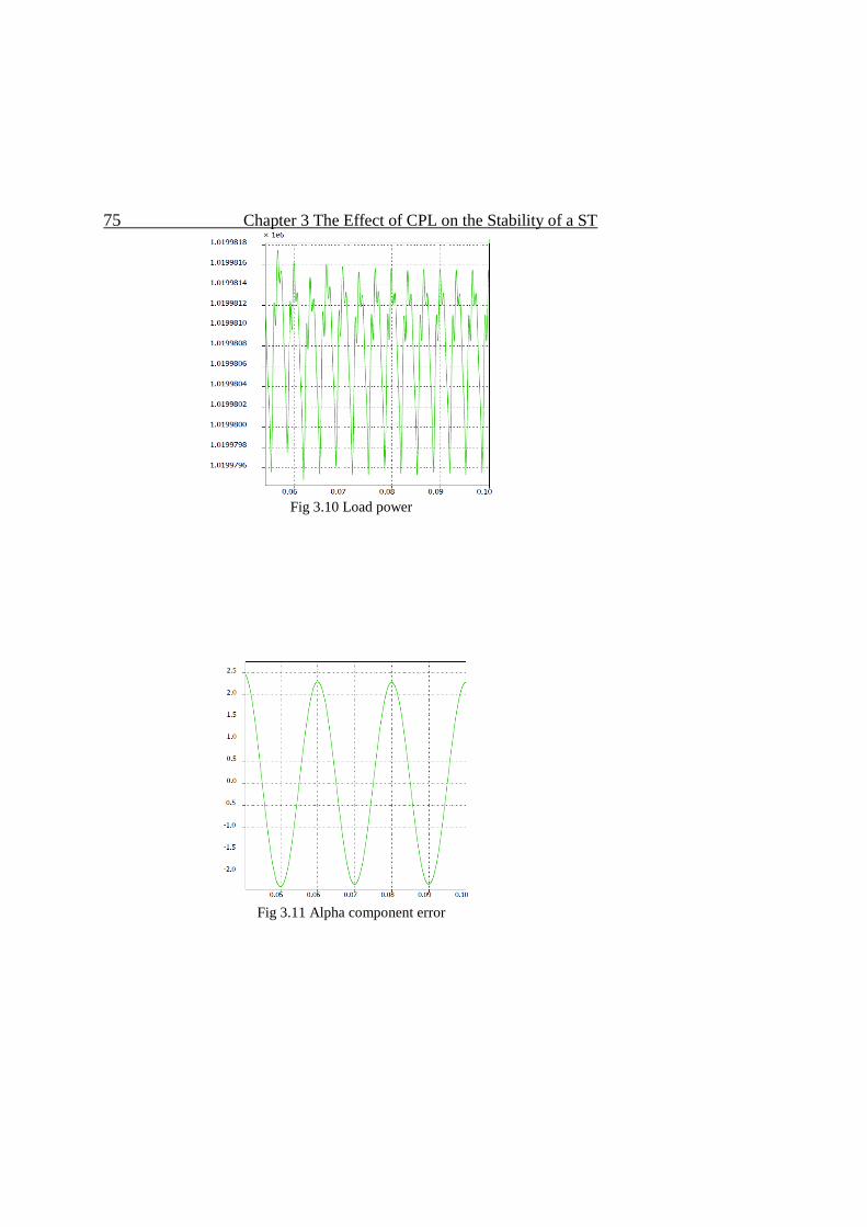
75 Chapter 3 The Effect of CPL on the Stability of a ST
Fig 3.10 Load power
Fig 3.11 Alpha component error
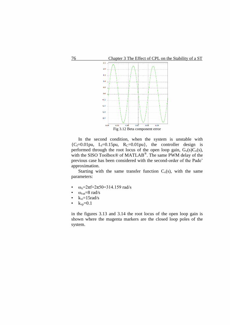
76 Chapter 3 The Effect of CPL on the Stability of a ST
Fig 3.12 Beta component error
In the second condition, when the system is unstable with
{Cf=0.01pu, Lf=0.15pu, RC=0.01pu}, the controller design is
performed through the root locus of the open loop gain, Gv(s)Cv(s),
with the SISO Toolbox® of MATLAB®. The same PWM delay of the
previous case has been considered with the second-order of the Pade’
approximation.
Starting with the same transfer function Cv(s), with the same
parameters:
• ωo=2πf=2π50=314.159 rad/s
• ωcut=8 rad/s
• kvi=15rad/s
• kvp=0.1
in the figures 3.13 and 3.14 the root locus of the open loop gain is
shown where the magenta markers are the closed loop poles of the
system.
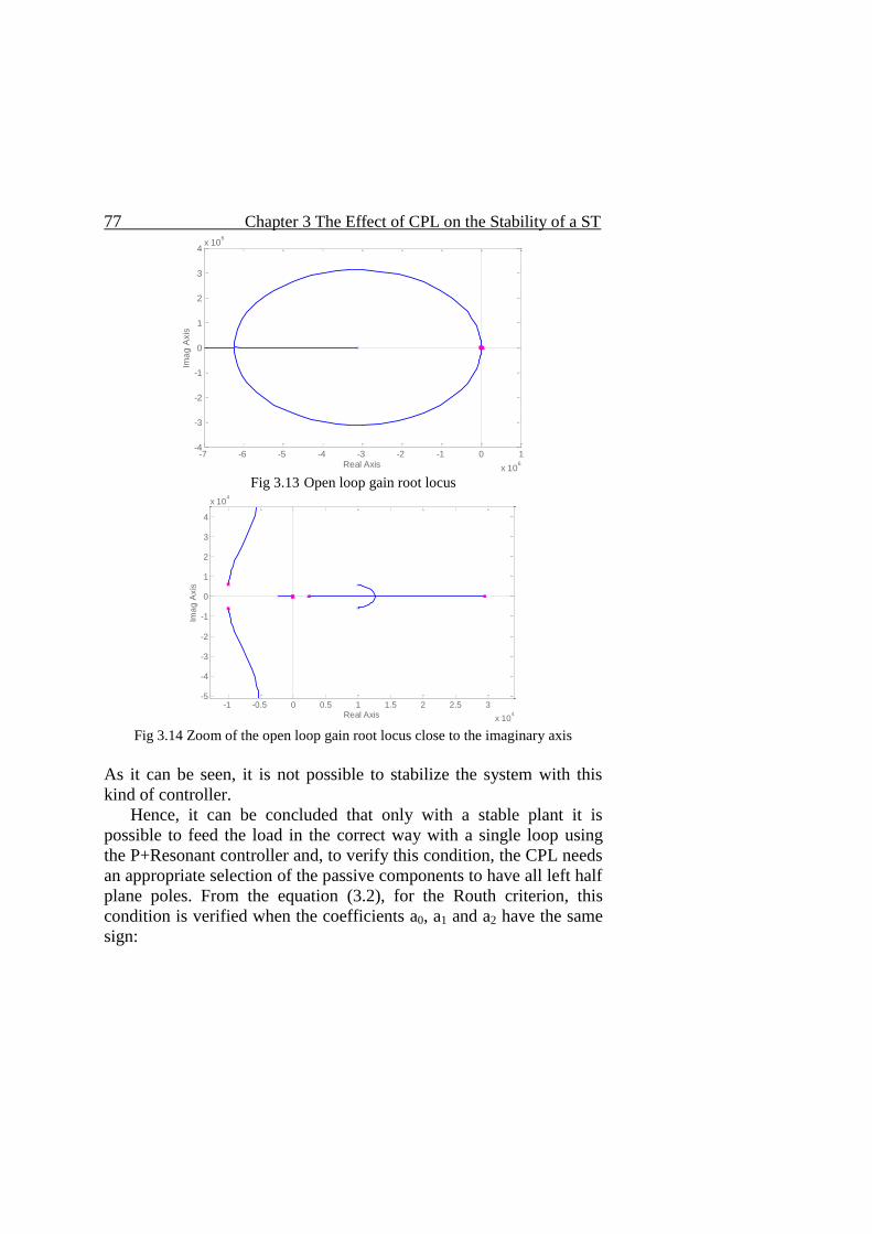
77 Chapter 3 The Effect of CPL on the Stability of a ST
-7 -6 -5 -4 -3 -2 -1 0 1
x 106
-4
-3
-2
-1
0
1
2
3
4x 10
6
Real Axis
Ima
g A
xis
Fig 3.13 Open loop gain root locus
Fig 3.14 Zoom of the open loop gain root locus close to the imaginary axis
As it can be seen, it is not possible to stabilize the system with this
kind of controller.
Hence, it can be concluded that only with a stable plant it is
possible to feed the load in the correct way with a single loop using
the P+Resonant controller and, to verify this condition, the CPL needs
an appropriate selection of the passive components to have all left half
plane poles. From the equation (3.2), for the Routh criterion, this
condition is verified when the coefficients a0, a1 and a2 have the same
sign:
-1 -0.5 0 0.5 1 1.5 2 2.5 3
x 104
-5
-4
-3
-2
-1
0
1
2
3
4
x 104
Real Axis
Ima
g A
xis
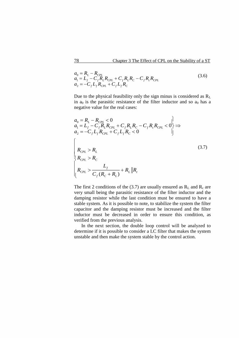
78 Chapter 3 The Effect of CPL on the Stability of a ST
0
1
2
L CPL
f f L CPL f L C f c CPL
f f CPL f f C
a R Ra L C R R C R R C R R
a C L R C L R
(3.6)
Due to the physical feasibility only the sign minus is considered as RL
in a0 is the parasitic resistance of the filter inductor and so a0 has a
negative value for the real cases:
0
1
2
00
0
( )
L CPL
f f L CPL f L C f c CPL
f f CPL f f C
CPL L
CPL C
f
CPL L c
f C L
a R Ra L C R R C R R C R R
a C L R C L R
R R
R R
LR R R
C R R
(3.7)
The first 2 conditions of the (3.7) are usually ensured as RL and Rc are
very small being the parasitic resistance of the filter inductor and the
damping resistor while the last condition must be ensured to have a
stable system. As it is possible to note, to stabilize the system the filter
capacitor and the damping resistor must be increased and the filter
inductor must be decreased in order to ensure this condition, as
verified from the previous analysis.
In the next section, the double loop control will be analyzed to
determine if it is possible to consider a LC filter that makes the system
unstable and then make the system stable by the control action.

79 Chapter 3 The Effect of CPL on the Stability of a ST
3.2 Double loop control analysis
The figure 3.15 shows the equivalent phase double loop control block
diagram.
Fig 3.15 Equivalent single phase double loop control block diagram
Considering the same system of the previous section:
• S=1MVA; Vrms=230V; RCPL=-0.158Ω; f=50Hz
under the abovementioned two conditions:
1) {Cf=0.15pu, Lf=0.01pu, RC=0.15pu} ( Condition 1)
2) {Cf=0.01pu, Lf=0.15pu, RC=0.01pu} ( Condition 2)
The controller design is performed with a Proportional Current
controller and a P+Resonant voltage controller looking at figure 3.15.
In this case, there is a plant for the inner current control loop and a
plant for the outer voltage control loop.
The plant for the inner current control loop is:

80 Chapter 3 The Effect of CPL on the Stability of a ST
1 0
2
2 1 0
1 f CPL f c
0
2 f f CPL f f C
1 f f L CPL f L C f C CPL
0 L CPL
s+ 1( )( )
( ) a s +a s + a
-C R + C R
1
-C L R +C L R
L - C R R C R R - C R R
R - R
Li
inv
b bi sG s
v s
b
b
a
a
a
(3.8)
The poles, of course, are the same of the single control loop while it is
present a right half plane zero z1=2475rad/s.
For this plant, with {Cf=0.15pu, Lf=0.01pu, RC=0.15pu}, the
proportional gain of the current controller has been selected in order to
have a more damped system for the outer loop [10], [11]:
I ipC (s) k 40 (3.9)
The plant for the outer voltage loop is:
i Iv c
i I
G (s)C (s)G (s) Z
1 G (s)C (s)
(3.10)
The poles are p1=-8.006e6rad/s and p2=2463rad/s.
The right half plane pole of the (3.10) cannot be eliminated with the
control action, changing the kip value, since it depends by the right
half plane zero in Gi(s) introduced by the constant power load.
The PWM has been modeled as a delay, τ=300μs, considering the
II order of the Pade’ approximation, as for the single loop analysis.
The P+Resonant voltage controller design is performed through
the root locus of the open loop gain, Gv(s)Cv(s), with the SISO
Toolbox® of MATLAB®. Starting with following parameters of
Cv(s):
• ωo=2πf=2π50=314.159rad/s
• ωcut=8 rad/s
• kvi=15 rad/s
• kvp=0.1
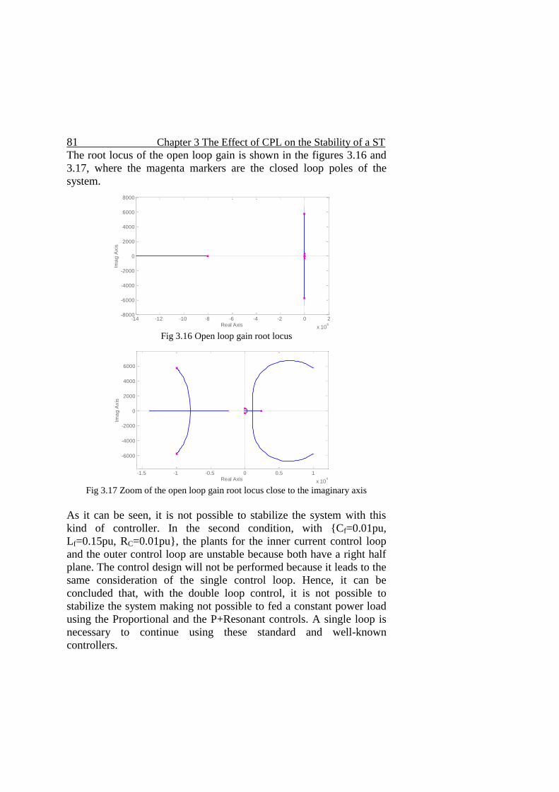
81 Chapter 3 The Effect of CPL on the Stability of a ST
The root locus of the open loop gain is shown in the figures 3.16 and
3.17, where the magenta markers are the closed loop poles of the
system.
-14 -12 -10 -8 -6 -4 -2 0 2
x 106
-8000
-6000
-4000
-2000
0
2000
4000
6000
8000
Real Axis
Ima
g A
xis
Fig 3.16 Open loop gain root locus
-1.5 -1 -0.5 0 0.5 1
x 104
-6000
-4000
-2000
0
2000
4000
6000
Real Axis
Ima
g A
xis
Fig 3.17 Zoom of the open loop gain root locus close to the imaginary axis
As it can be seen, it is not possible to stabilize the system with this
kind of controller. In the second condition, with {Cf=0.01pu,
Lf=0.15pu, RC=0.01pu}, the plants for the inner current control loop
and the outer control loop are unstable because both have a right half
plane. The control design will not be performed because it leads to the
same consideration of the single control loop. Hence, it can be
concluded that, with the double loop control, it is not possible to
stabilize the system making not possible to fed a constant power load
using the Proportional and the P+Resonant controls. A single loop is
necessary to continue using these standard and well-known
controllers.
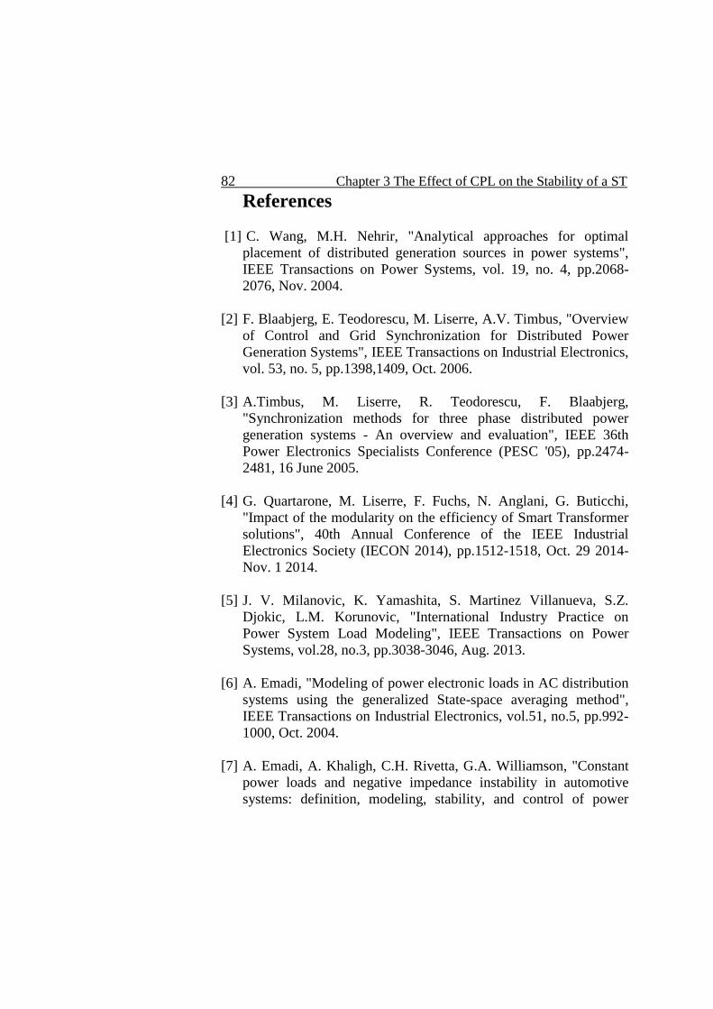
82 Chapter 3 The Effect of CPL on the Stability of a ST
References
[1] C. Wang, M.H. Nehrir, "Analytical approaches for optimal
placement of distributed generation sources in power systems",
IEEE Transactions on Power Systems, vol. 19, no. 4, pp.2068-
2076, Nov. 2004.
[2] F. Blaabjerg, E. Teodorescu, M. Liserre, A.V. Timbus, "Overview
of Control and Grid Synchronization for Distributed Power
Generation Systems", IEEE Transactions on Industrial Electronics,
vol. 53, no. 5, pp.1398,1409, Oct. 2006.
[3] A.Timbus, M. Liserre, R. Teodorescu, F. Blaabjerg,
"Synchronization methods for three phase distributed power
generation systems - An overview and evaluation", IEEE 36th
Power Electronics Specialists Conference (PESC '05), pp.2474-
2481, 16 June 2005.
[4] G. Quartarone, M. Liserre, F. Fuchs, N. Anglani, G. Buticchi,
"Impact of the modularity on the efficiency of Smart Transformer
solutions", 40th Annual Conference of the IEEE Industrial
Electronics Society (IECON 2014), pp.1512-1518, Oct. 29 2014-
Nov. 1 2014.
[5] J. V. Milanovic, K. Yamashita, S. Martinez Villanueva, S.Z.
Djokic, L.M. Korunovic, "International Industry Practice on
Power System Load Modeling", IEEE Transactions on Power
Systems, vol.28, no.3, pp.3038-3046, Aug. 2013.
[6] A. Emadi, "Modeling of power electronic loads in AC distribution
systems using the generalized State-space averaging method",
IEEE Transactions on Industrial Electronics, vol.51, no.5, pp.992-
1000, Oct. 2004.
[7] A. Emadi, A. Khaligh, C.H. Rivetta, G.A. Williamson, "Constant
power loads and negative impedance instability in automotive
systems: definition, modeling, stability, and control of power
83 Chapter 3 The Effect of CPL on the Stability of a ST
electronic converters and motor drives", IEEE Transactions on
Vehicular Technology, vol.55, no.4, pp.1112-1125, July 2006.
[8] D. P. Ariyasinghe, D.M. Vilathgamuwa, "Stability analysis of
microgrids with constant power loads", IEEE International
Conference on Sustainable Energy Technologies (ICSET 2008),
pp.279-284, 24-27 Nov. 2008.
[9] D. M. Vilathgamuwa, X.N. Zhang, S.D.G. Jayasinghe, B.S.
Bhangu, C.J. Gajanayake, King Jet Tseng, "Virtual resistance
based active damping solution for constant power instability in AC
microgrids," 37th Annual Conference on IEEE Industrial
Electronics Society (IECON 2011), pp.3646-3651, 7-10 Nov.
2011.
[10] Poh Chiang Loh, D.G. Holmes, "Analysis of multiloop control
strategies for LC/CL/LCL-filtered voltage-source and current-
source inverters," IEEE Transactions on Industry Applications,
vol.41, no.2, pp.644-654, March-April 2005.
[11] Yun Wei Li, "Control and Resonance Damping of Voltage-
Source and Current-Source Converters With LC Filters," IEEE
Transactions on Industrial Electronics, vol.56, no.5, pp.1511-1521,
May 2009.
Chapter 4
Minimum Computing MPPT
The wide interest for Maximum Power Point Tracking (MPPT)
control is justified by the attempt to maximize the energy harvested
from photovoltaic sources in all the operating conditions. Several
control techniques can be adopted [1]-[10], both analog and digital, to
achieve good MPPT efficiency. Digital techniques are best suited to
implement adaptive control. The runtime optimization of MPPT
digital control is in the focus of many studies, mostly regarding the
Perturb&Observe (P&O) technique described in the chapter 1. The
two parameters determining the MPPT efficiency and the tracking
speed P&O technique are the sampling period TMPPT and the duty-
cycle step perturbation magnitude D.
There are a lot of techniques to select these 2 parameters. For
example:
D is updated based on the sampled ratio I/D and TMPPT is
consequently set as smaller as D decreases [1].
A fuzzy technique is adopted to select D, considering both
the power and current variations P and I [2].
D is corrected based on P/V ratio [3].
D is set proportional to P [4], [5].
The previous techniques involve a continuous update of D which
can lead to temporary P&O swing around the MPP with oscillations
across more than 3 operating points. A simplified approach using two
D values, a big one to improve MPP tracking capabilities when sun
irradiance is rapidly varying, and a small one adopted for steady
operation can be adopted [6]. The use of two D values only does not
guarantee maximum energy harvesting in all operating conditions. In
[7] the duty perturbation ΔD is set as smaller as the panel voltage is
closer to the theoretical MPP. Such approach needs a preliminary
modeling of the PV source and cannot guarantee high MPPT
85 Chapter 4 Minimum Computing MPPT
efficiency. In [8] some adaptive MPPT methods are overviewed and a
technique is proposed wherein the convergence to optimum MPPT is
driven by an exponential adaptation law. In [9] the power variation ΔP
is used as error signal to correct the duty-cycle reference by means of
PI compensation. In [10] an FPGA controller is discussed wherein the
optimal sampling period TMPPT setup is achieve based on a system
response estimation done through FFT. The level of MPPT efficiency
achievable by the techniques mentioned above is conditioned by many
factors, such as the modeling assumptions, the duty-cycle and
sampling period correction law adopted and the computing
capabilities of the digital device adopted for the control
implementation. To this regard, all of them involve a variable amount
of computations, including the calculation of the ratios (e.g. I/D,
P/V) used as figure of merit, the subsequent calculations required
by the adaptation law and the additional calculations required by
specific estimation/decision algorithm used. As a consequence, many
methods and algorithms yield high MPPT efficiency at the price of
high computing effort, which is not compatible with low cost
requirements. This issue is stressed in applications where a single
digital device is wanted to perform multiple control functions, such as,
for example, the LED lighting systems fed by PV sources [11],
eventually including an energy storage device. In such situations,
different dc-dc converters are involved in the source-side regulation
and in the load-side regulation, and a single device must control the
MPPT converter, the dimmable LED converter and the bulk voltage to
manage the storage device status. More in general, achieving
maximum energy harvesting with minimum cost devices is a
fundamental renewable energy industry demand.
The method presented realizes the real time adaptation of a
photovoltaic P&O MPPT control with minimum computing effort to
maximize the PV energy harvesting against changes of sun irradiation,
the temperature and the characteristics of the PV source and by the
overall system the PV source is part of. It exploits the correlation
existing among the MPPT efficiency and the onset of a permanent 3
levels quantized oscillation around the MPP that is the steady-state
condition for the algorithm. Like in [12], the method detects this
steady-state condition and, based on that, changes the MPPT
parameters. A comparison between the proposed method and the one
86 Chapter 4 Minimum Computing MPPT
presented in [12] will be done through PSIM® simulations to set
exactly the same test conditions.
As a multi-function control application case study, a
TMS320F28035 Texas Instruments Piccolo™ Microcontroller (µc) is
used to implement the adaptive PV MPPT control algorithm, the LED
driver dimming control and the bulk voltage control of a 70W LED
lighting system prototype fed by a photovoltaic source with a
capacitor working as storage device. The choice of the F28035 µc is
carried out to use the same family, the TI C2000, that ABB Solar
Group implements on its converters but with a single-core system as
the goal of the proposed method is the minimum computing effort.
Hence the aim of this chapter is to determine an optimize MPPT
algorithm that can be implemented in the ABB Solar Group systems.
4.1 Light-to-Light system case study
The figure 4.1 shows the block diagram of the system under study. It
is composed by a PV panel, a LED array, a boost dc–dc converter for
the MPPT of the PV panel and a buck dc–dc converter for driving the
LEDs array.
Fig. 4.1 Light to Light System

87 Chapter 4 Minimum Computing MPPT
The global system control goal is to harvest the maximum PV
energy to feed a dimmable LEDs array. Energy storage and loads
dimming is an effective mean to implement intelligent energy
management solutions [11] when energy generated by renewable
sources is involved. In fact, photovoltaic inverters with storage and
load management capabilities are highly appealing today. To this
regard, the block diagram of the figure 4.1 can be considered as a
general system concept, as the LEDs array can be replaced by any
kind of dimmable load and the storage device can be a capacitor, a
super capacitor or a battery. The overall control algorithm modulates
the bulk voltage to balance the instant power between the PV source
and the LEDs array through the storage device charge and discharge,
while modulates the LEDs array dimming to balance the instant power
between the PV source and the storage device when its voltage or
current exceeds the allowed operating ranges. The LEDs array is
driven by a hysteretic controller ensuring constant current operation
and using an enable command to dimm the driver.
The P&O technique is still today the simplest and cheapest mean
to achieve photovoltaic MPPT. Indeed, the dramatic fall of
microcontrollers cost helps in implementing quite inexpensive MPPT
controllers. The energy harvesting effectiveness of P&O depends on
sampling period and step perturbation magnitude setup [13]. MPPT
high dynamic promptness is required to fastly track rapidly changing
irradiation conditions, while small oscillations around the MPP are
required in steady state conditions. These two conditions are
conflicting for MPPT setup, as energy harvesting is improved by large
magnitude step perturbations in the former and minimum step
perturbations in the latter. The adaptive methods for perturbative
MPPT controls try to achieve a tradeoff in the setup of the
perturbation magnitude by means of adaptation laws based on the
elaboration of sampled voltage, current, power and duty-cycle. The
effectiveness of such approaches is heavily conditioned by modeling
assumptions and by the type of adaptation law, mostly based on gain
and shift factors and algorithms whose optimal setup just lifts the
problem to a different layer. However, there is a universal property of
P&O technique allowing achieving easy optimal MPPT setup.
88 Chapter 4 Minimum Computing MPPT
4.2 Adaptive duty-cycle setup
The figure 4.2 shows the voltage, current and power of a PV panel
operating with a P&O MPPT controller based on Open-Loop (OL-
MPPT) cycle-by-cycle duty-cycle step perturbation D[k]. A correct
P&O MPPT steady-state operation involves a 3 points oscillation
across the MPP as shown in the figure 4.2 (a), (b) and (c).
(a)
(b)
89 Chapter 4 Minimum Computing MPPT
(c)
Fig. 4.2. Open-Loop P&O MPPT 3 points operation with TMPPT=10ms.
The smaller the duty-cycle step perturbation D, the higher the
energy harvested cycle-by-cycle in steady state [13]. In theory, the
best would be to drop D[k] magnitude at the minimum value allowed
by the microcontroller used to implement the MPPT control.
Regarding the sampling period TMPPT, we also get energy harvesting
benefits in reducing it [13] in dynamic irradiance conditions.
However, the sign of duty-cycle perturbation for k+1-th cycle,
sign(D[k+1]), is based on the sign of power variation, sign(P[k]), at
the end of the k-th cycle. The combined effect of irradiance variations,
voltage and current measurement errors, quantization, poorly damped
system transients, sampling period shortness and too small D[k+1]
can lead the operation of the P&O MPPT controller into a four, or
more, points oscillations around the MPP, as shown in the figure 4.3
(a), (b) and (c). In this case the system works in an unpredictable way,
not ensuring maximum energy harvesting.
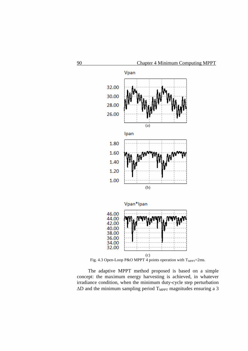
90 Chapter 4 Minimum Computing MPPT
(a)
(b)
(c)
Fig. 4.3 Open-Loop P&O MPPT 4 points operation with TMPPT=2ms.
The adaptive MPPT method proposed is based on a simple
concept: the maximum energy harvesting is achieved, in whatever
irradiance condition, when the minimum duty-cycle step perturbation
D and the minimum sampling period TMPPT magnitudes ensuring a 3
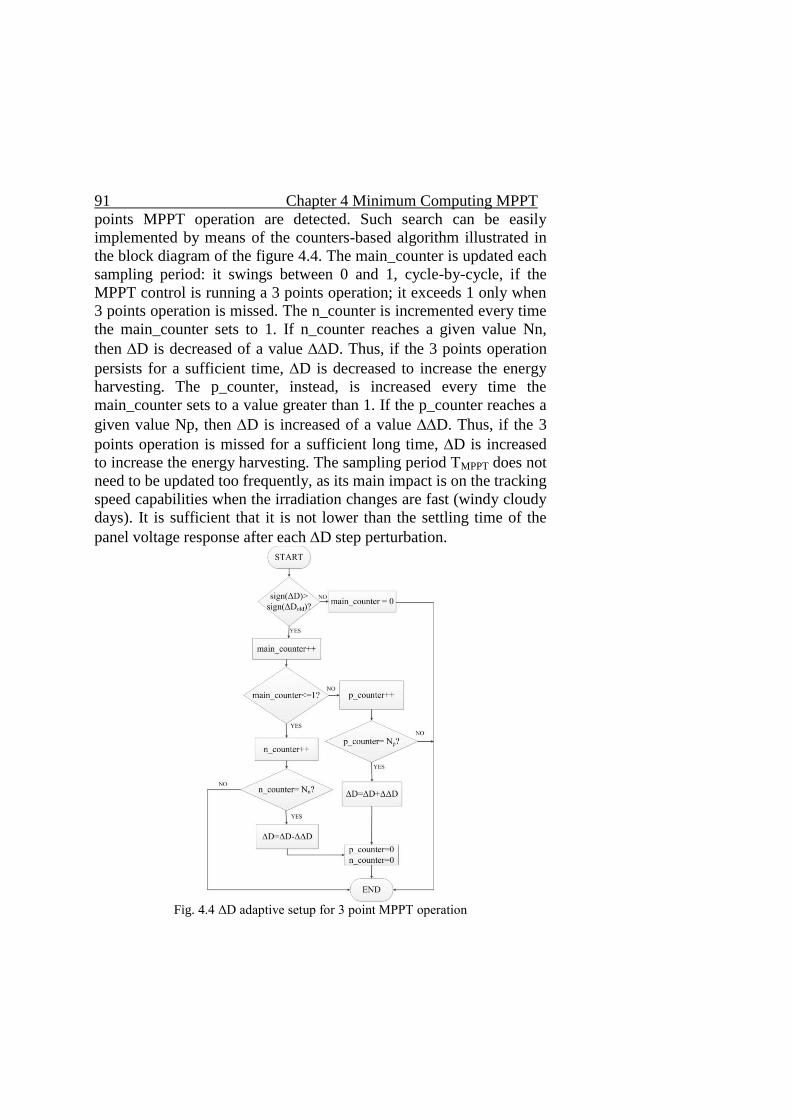
91 Chapter 4 Minimum Computing MPPT
points MPPT operation are detected. Such search can be easily
implemented by means of the counters-based algorithm illustrated in
the block diagram of the figure 4.4. The main_counter is updated each
sampling period: it swings between 0 and 1, cycle-by-cycle, if the
MPPT control is running a 3 points operation; it exceeds 1 only when
3 points operation is missed. The n_counter is incremented every time
the main_counter sets to 1. If n_counter reaches a given value Nn,
then D is decreased of a value D. Thus, if the 3 points operation
persists for a sufficient time, D is decreased to increase the energy
harvesting. The p_counter, instead, is increased every time the
main_counter sets to a value greater than 1. If the p_counter reaches a
given value Np, then D is increased of a value D. Thus, if the 3
points operation is missed for a sufficient long time, D is increased
to increase the energy harvesting. The sampling period TMPPT does not
need to be updated too frequently, as its main impact is on the tracking
speed capabilities when the irradiation changes are fast (windy cloudy
days). It is sufficient that it is not lower than the settling time of the
panel voltage response after each D step perturbation.
Fig. 4.4 ΔD adaptive setup for 3 point MPPT operation
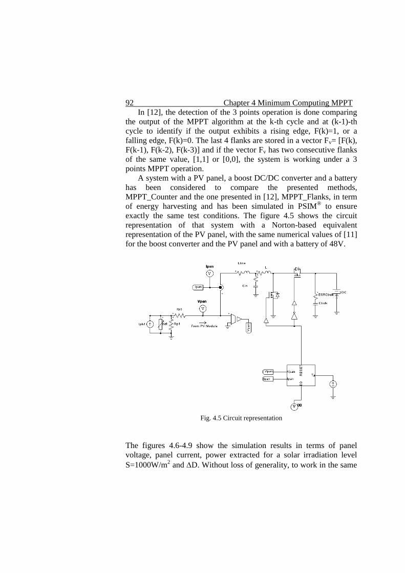
92 Chapter 4 Minimum Computing MPPT
In [12], the detection of the 3 points operation is done comparing
the output of the MPPT algorithm at the k-th cycle and at (k-1)-th
cycle to identify if the output exhibits a rising edge, F(k)=1, or a
falling edge, F(k)=0. The last 4 flanks are stored in a vector Fv= [F(k),
F(k-1), F(k-2), F(k-3)] and if the vector Fv has two consecutive flanks
of the same value, [1,1] or [0,0], the system is working under a 3
points MPPT operation.
A system with a PV panel, a boost DC/DC converter and a battery
has been considered to compare the presented methods,
MPPT_Counter and the one presented in [12], MPPT_Flanks, in term
of energy harvesting and has been simulated in PSIM®
to ensure
exactly the same test conditions. The figure 4.5 shows the circuit
representation of that system with a Norton-based equivalent
representation of the PV panel, with the same numerical values of [11]
for the boost converter and the PV panel and with a battery of 48V.
Fig. 4.5 Circuit representation
The figures 4.6-4.9 show the simulation results in terms of panel
voltage, panel current, power extracted for a solar irradiation level
S=1000W/m2 and D. Without loss of generality, to work in the same
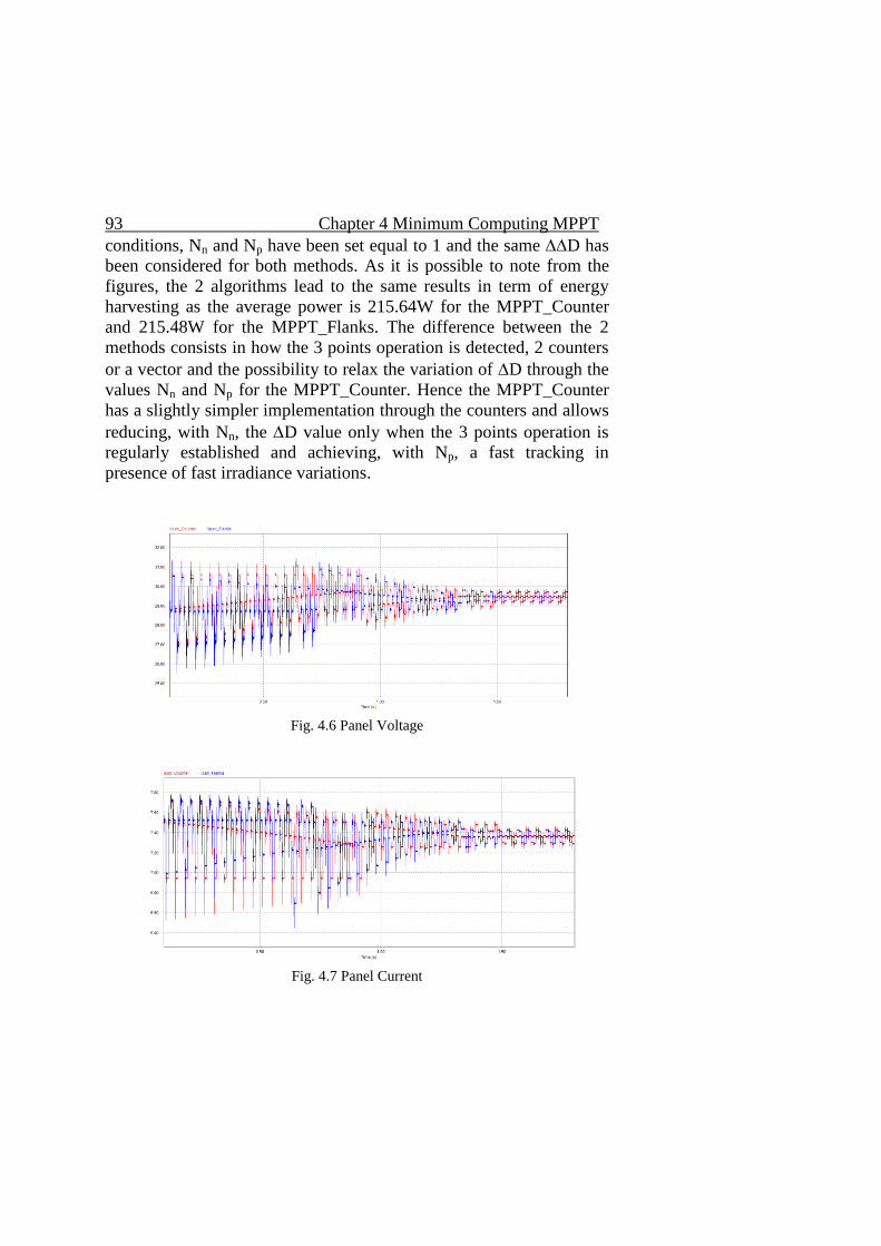
93 Chapter 4 Minimum Computing MPPT
conditions, Nn and Np have been set equal to 1 and the same D has
been considered for both methods. As it is possible to note from the
figures, the 2 algorithms lead to the same results in term of energy
harvesting as the average power is 215.64W for the MPPT_Counter
and 215.48W for the MPPT_Flanks. The difference between the 2
methods consists in how the 3 points operation is detected, 2 counters
or a vector and the possibility to relax the variation of D through the
values Nn and Np for the MPPT_Counter. Hence the MPPT_Counter
has a slightly simpler implementation through the counters and allows
reducing, with Nn, the D value only when the 3 points operation is
regularly established and achieving, with Np, a fast tracking in
presence of fast irradiance variations.
Fig. 4.6 Panel Voltage
Fig. 4.7 Panel Current
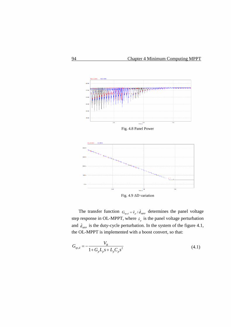
94 Chapter 4 Minimum Computing MPPT
Fig. 4.8 Panel Power
Fig. 4.9 ΔD variation
The transfer function ,
ˆˆ /vp d p MPPG v d determines the panel voltage
step response in OL-MPPT, where ˆpv is the panel voltage perturbation
and ˆMPPd is the duty-cycle perturbation. In the system of the figure 4.1,
the OL-MPPT is implemented with a boost convert, so that:
, 21
Bvp d
p p p p
VG
G L s L C s (4.1)
95 Chapter 4 Minimum Computing MPPT
where Lp is the inductance, Cp is the capacitance, Gp is the PV panel
conductance and VB is the dc bulk voltage. According to (4.1), the
panel voltage response to D step perturbation settles to its final value
with absolute error || within the time:
2ln(| /2)
p
P p
CT
G L (4.2)
The values of Lp and Cp are known from boost power stage design.
The value of Gp can be determined run-time from the samples of panel
voltage and current acquired for MPPT control.
4.3 LED Dimming-based Bulk Voltage
regulation
Thanks to low computing needs of adaptive MPPT described in
previous section, a single microcontroller can be used to implement
the other control functions needed by a system like the one shown in
the figure 4.1. As illustrated, the aim of that system is to ensure
maximum energy harvesting from the PV source and adequate power
balance among the PV source, the load and the storage device. This
multiple tasks can be implemented through an adequate dynamic
control of the bulk voltage vB. The design of compensation network
for Bulk Voltage Control (BVC) can be realized based on the dynamic
model of the system, treated in [11], where analog BVC was discussed
and experimented.
The control signal generated by the BVC loop modulates the
dimming duty-cycle Ddim of the LED driver, as shown in the figure
4.1. The dimming frequency fdim must be much smaller than the
switching frequency fLED, to avoid flickering of LEDs light. For the
case under study, it is fdim=3kHz and fLED=400kHz.
The uncompensated BVC loop gain of the system in the figure 4.1
is given by (4.3):
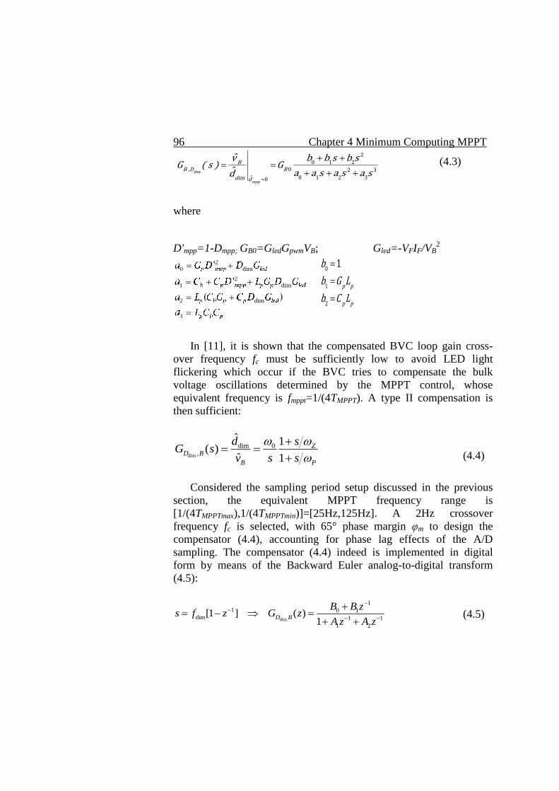
96 Chapter 4 Minimum Computing MPPT
dim
mpp
BB ,D B
ˆdim d
ˆ b b s b svG ( s ) G
ˆ a a s a s a sd
2
0 1 20 2 3
0 1 2 30
(4.3)
where
D'mpp=1-Dmpp; GB0=GledGpwmVB; Gled=-VFIF/VB2
2
0 dim
2
1 dim
2 dim
3
'
'
( )
p p
p p
b
b G L
b C L
0
1
2
1
In [11], it is shown that the compensated BVC loop gain cross-
over frequency fc must be sufficiently low to avoid LED light
flickering which occur if the BVC tries to compensate the bulk
voltage oscillations determined by the MPPT control, whose
equivalent frequency is fmppt=1/(4TMPPT). A type II compensation is
then sufficient:
dim
dim 0,
ˆ 1( )
ˆ 1
ZD B
B P
d sG s
v s s
(4.4)
Considered the sampling period setup discussed in the previous
section, the equivalent MPPT frequency range is
[1/(4TMPPTmax),1/(4TMPPTmin)]=[25Hz,125Hz]. A 2Hz crossover
frequency fc is selected, with 65° phase margin φm to design the
compensator (4.4), accounting for phase lag effects of the A/D
sampling. The compensator (4.4) indeed is implemented in digital
form by means of the Backward Euler analog-to-digital transform
(4.5):
dim,
11 0 1
dim 1 1
1 2
[1 ] ( )1
D B
B B zs f z G z
A z A z
(4.5)
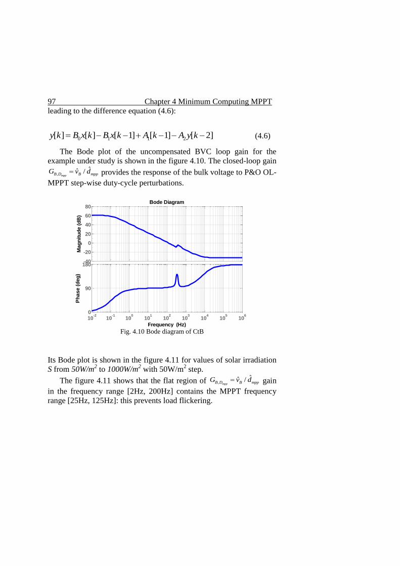
97 Chapter 4 Minimum Computing MPPT
leading to the difference equation (4.6):
0 1 1 2[ ] [ ] [ 1] [ 1] [ 2] y k B x k B x k A k A y k
(4.6)
The Bode plot of the uncompensated BVC loop gain for the
example under study is shown in the figure 4.10. The closed-loop gain
,ˆˆ /
mppB D B mppG v d provides the response of the bulk voltage to P&O OL-
MPPT step-wise duty-cycle perturbations.
-40
-20
0
20
40
60
80
Mag
nit
ud
e (
dB
)
10-2
10-1
100
101
102
103
104
105
106
0
90
180
Ph
ase (
deg
)
Bode Diagram
Frequency (Hz) Fig. 4.10 Bode diagram of CtB
Its Bode plot is shown in the figure 4.11 for values of solar irradiation
S from 50W/m2 to 1000W/m
2 with 50W/m
2 step.
The figure 4.11 shows that the flat region of ,ˆˆ /
mppB D B mppG v d gain
in the frequency range [2Hz, 200Hz] contains the MPPT frequency
range [25Hz, 125Hz]: this prevents load flickering.
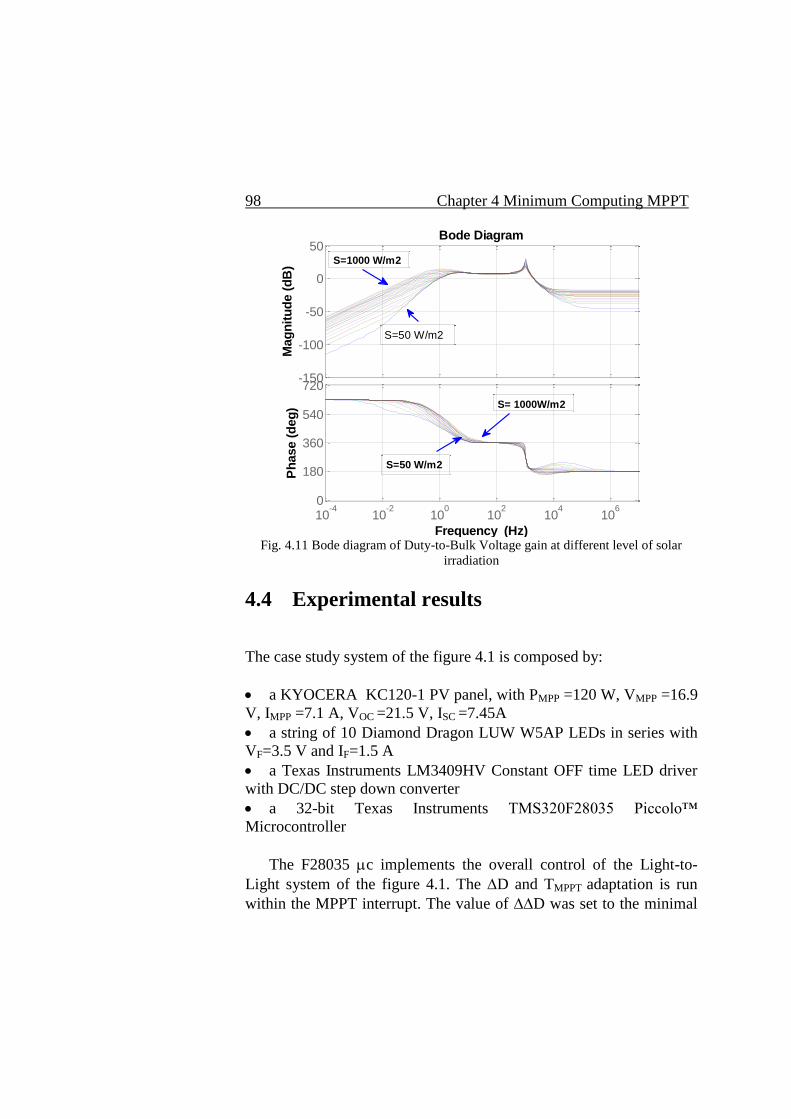
98 Chapter 4 Minimum Computing MPPT
-150
-100
-50
0
50
Mag
nit
ud
e (
dB
)
10-4
10-2
100
102
104
106
0
180
360
540
720
Ph
ase (
deg
)
Bode Diagram
Frequency (Hz)
S=1000 W/m2
S=50 W/m2
S=50 W/m2
S= 1000W/m2
Fig. 4.11 Bode diagram of Duty-to-Bulk Voltage gain at different level of solar
irradiation
4.4 Experimental results
The case study system of the figure 4.1 is composed by:
a KYOCERA KC120-1 PV panel, with PMPP =120 W, VMPP =16.9
V, IMPP =7.1 A, VOC =21.5 V, ISC =7.45A
a string of 10 Diamond Dragon LUW W5AP LEDs in series with
VF=3.5 V and IF=1.5 A
a Texas Instruments LM3409HV Constant OFF time LED driver
with DC/DC step down converter
a 32-bit Texas Instruments TMS320F28035 Piccolo™
Microcontroller
The F28035 c implements the overall control of the Light-to-
Light system of the figure 4.1. The D and TMPPT adaptation is run
within the MPPT interrupt. The value of D was set to the minimal
99 Chapter 4 Minimum Computing MPPT
possible value allowed by the F28035 c, which corresponds to a
signal tick:
60min 100 100 0.1%
60
CLK
PWM
f kHzD
f MHz (4.7)
The values of Nn and Np thresholds have been fixed at 120 and 5,
respectively. The high Nn value is justified by the need to reduce the
duty-cycle step magnitude D only when a 3 points operation is
regularly established. The small Np value is justified by the need to
achieve a fast tracking in presence of fast irradiance variations. D is
also subjected to an upper limit to avoid large oscillations around the
MPP. The sampling period TMPPT resolution is 0.1ms. Starting from
nominal TMPPT = 10ms, the F28035 c realizes a low frequency
periodic TMPPT adaptation, according to the differential PV instant
panel conductance Gp.
The figures 4.12 and 4.13 show the experimental measurements of
panel voltage, current and power, in low and high irradiance
conditions, without and with adapted D, for a fixed sampling period
value TMPPT. The power waveforms show lower magnitude
oscillations as a consequence of the D adaptation. The figures 4.14
and 4.15 show the effects of TMPPT adaptation. In this case, no
improvement is expected about the energy harvesting efficiency;
rather, it is evident that the next perturbation of OL-MPPT acts
suddenly after the panel voltage settles. The performances of the BVC
have been validated too.
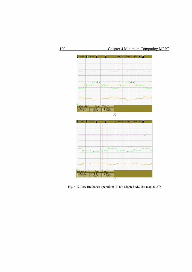
100 Chapter 4 Minimum Computing MPPT
(a)
(b)
Fig. 4.12 Low irradiance operation: (a) not adapted ΔD, (b) adapted ΔD
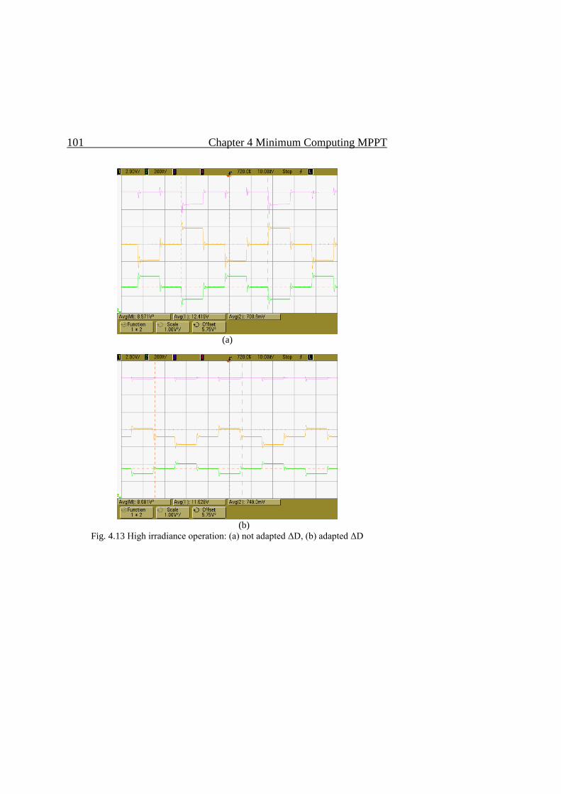
101 Chapter 4 Minimum Computing MPPT
(a)
(b)
Fig. 4.13 High irradiance operation: (a) not adapted ΔD, (b) adapted ΔD
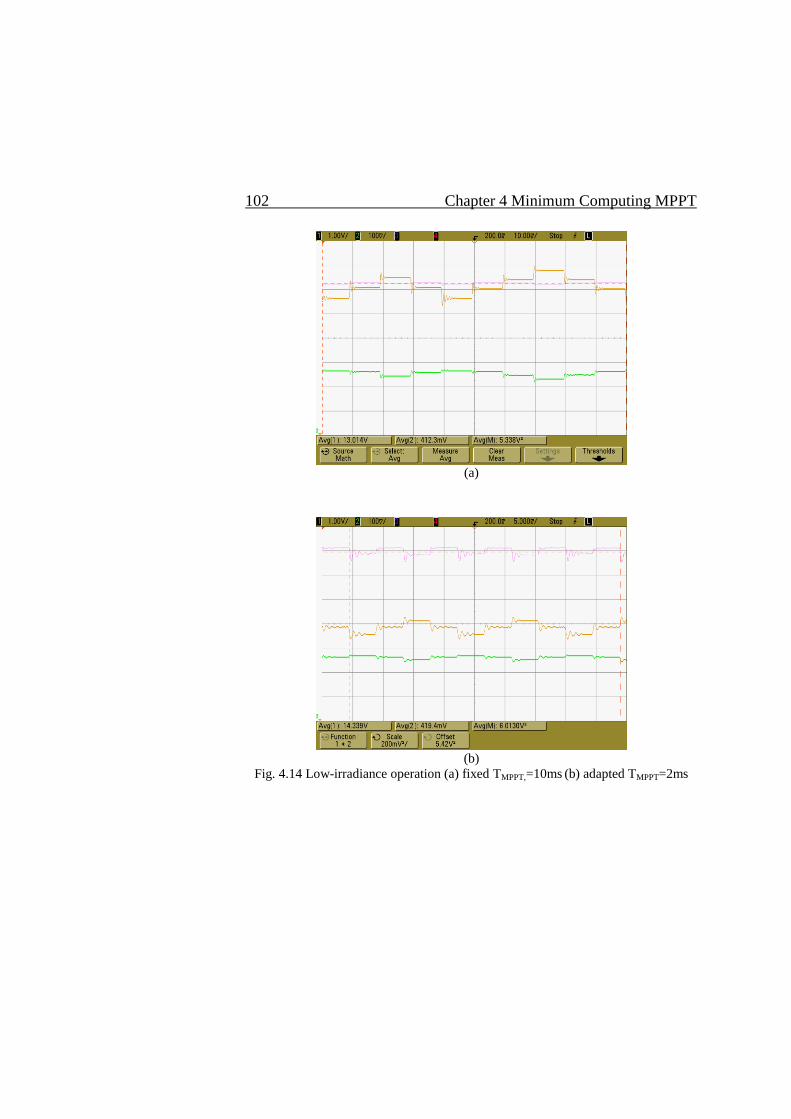
102 Chapter 4 Minimum Computing MPPT
(a)
(b)
Fig. 4.14 Low-irradiance operation (a) fixed TMPPT,=10ms (b) adapted TMPPT=2ms
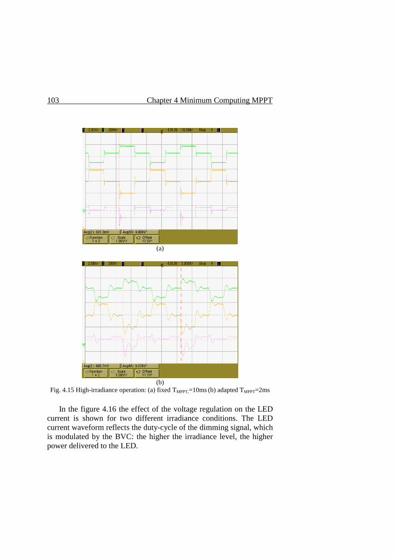
103 Chapter 4 Minimum Computing MPPT
(a)
(b)
Fig. 4.15 High-irradiance operation: (a) fixed TMPPT,=10ms (b) adapted TMPPT=2ms
In the figure 4.16 the effect of the voltage regulation on the LED
current is shown for two different irradiance conditions. The LED
current waveform reflects the duty-cycle of the dimming signal, which
is modulated by the BVC: the higher the irradiance level, the higher
power delivered to the LED.
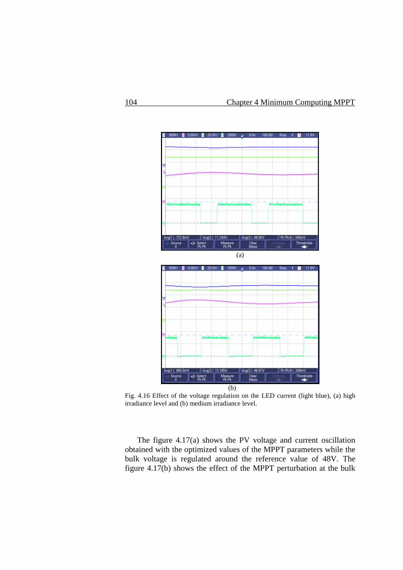
104 Chapter 4 Minimum Computing MPPT
(a)
(b)
Fig. 4.16 Effect of the voltage regulation on the LED current (light blue), (a) high
irradiance level and (b) medium irradiance level.
The figure 4.17(a) shows the PV voltage and current oscillation
obtained with the optimized values of the MPPT parameters while the
bulk voltage is regulated around the reference value of 48V. The
figure 4.17(b) shows the effect of the MPPT perturbation at the bulk

105 Chapter 4 Minimum Computing MPPT
voltage. As expected, the bulk capacitor absorbs the power fluctuation
coming from the PV side, the bulk voltage follows the MPPT
oscillations and the power delivered to the LED remains constant. An
important outcome of such operation mode is an improvement of the
P&O OL-MPPT energy harvesting capabilities. In fact, when the
output voltage of the dc-dc converter used to implement the MPPT is
tightly regulated, namely it is almost constant; each step-up D
perturbation involves a step-down variation on the panel voltage only,
and vice-versa. Instead, if the output voltage of the dc-dc converter is
allowed to swing, following the step-wise D perturbation, it happens
that each step-up D perturbation involves as a step-down variation
on the panel voltage as a step-up in the output converter voltage. In
this way, for whatever D magnitude, the oscillations on the panel
voltage will be reduced with respect to the case of tightly regulated
output voltage. The previous discussion highlights that, in case the
storage device is a battery, it has to be interfaced with the bulk by
means of a power converter allowing free swing of the bulk voltage at
the MPPT frequency, if true maximum PV energy harvesting is
desired. In other words, it is not the best for true maximum PV energy
harvesting operation if the output of the dc-dc converter implementing
the P&O OL-MPPT is terminated onto a device involving, or
requiring, a tightly regulated voltage.
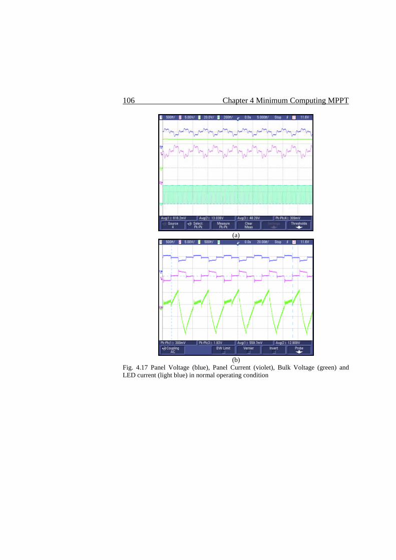
106 Chapter 4 Minimum Computing MPPT
(a)
(b)
Fig. 4.17 Panel Voltage (blue), Panel Current (violet), Bulk Voltage (green) and
LED current (light blue) in normal operating condition
107 Chapter 4 Minimum Computing MPPT
References
[1] Yuncong Jiang; Qahouq, J.A.A.; Haskew, T.A., "Adaptive Step
Size With Adaptive-Perturbation-Frequency Digital MPPT
Controller for a Single-Sensor Photovoltaic Solar System", IEEE
Transactions on Power Electronics, vol.28, no.7, pp.3195,3205,
July 2013.
[2] Mohd Zainuri, M.A.A.; Mohd Radzi, M.A.; Soh, A.C.; Rahim,
N.A., "Adaptive P&O-fuzzy control MPPT for PV boost dc-dc
converter", IEEE International Conference on Power and Energy
(PECon), pp.524,529, 2-5 Dec. 2012.
[3] Al-Diab, A.; Sourkounis, C., "Variable step size P&O MPPT
algorithm for PV systems", 12th International Conference on
Optimization of Electrical and Electronic Equipment (OPTIM),
pp.1097,1102, 20-22 May 2010.
[4] Khaehintung, N.; Wiangtong, T.; Sirisuk, P., "FPGA
Implementation of MPPT Using Variable Step-Size P&O
Algorithm for PV Applications", International Symposium on
Communications and Information Technologies (ISCIT '06),
pp.212,215, Oct. 18 2006-Sept. 20 2006.
[5] Weidong Xiao; Dunford, W.G., "A modified adaptive hill
climbing MPPT method for photovoltaic power systems", IEEE
35th Annual Power Electronics Specialists Conference (PESC
'04), pp.1957,1963 Vol.3, 20-25 June 2004.
[6] Chao Zhang; Dean Zhao; Jinjing Wang; Guichang Chen, "A
modified MPPT method with variable perturbation step for
photovoltaic system", IEEE 6th International Power Electronics
and Motion Control Conference (IPEMC '09), pp.2096,2099, 17-
20 May 2009.
[7] Piegari, L.; Rizzo, R., "Adaptive perturb and observe algorithm for
photovoltaic maximum power point tracking", Renewable Power
Generation (IET), vol.4, no.4, pp.317,328, July 2010.
108 Chapter 4 Minimum Computing MPPT
[8] Buyukdegirmenci, V.T.; Bazzi, A.M.; Krein, P.T., "A comparative
study of an exponential adaptive perturb and observe algorithm
and ripple correlation control for real-time optimization", IEEE
12th Workshop on Control and Modeling for Power Electronics
(COMPEL), pp.1,8, 28-30 June 2010.
[9] Abdelsalam, A.K.; Massoud, A.M.; Ahmed, S.; Enjeti, P., "High-
Performance Adaptive Perturb and Observe MPPT Technique for
Photovoltaic-Based Microgrids", IEEE Transactions on Power
Electronics, vol.26, no.4, pp.1010,1021, April 2011.
[10] P. Manganiello, M. Ricco, E. Monmasson, G. Petrone, G.
Spagnuolo, "On-line optimization of the P&O MPPT method by
means of the system identification," Industrial Electronics Society,
39th Annual Conference of the IEEE (IECON), pp.1786,1791, 10-
13 Nov. 2013.
[11] Femia, N.; Fortunato, M.; Vitelli, M., "Light-to-Light: PV-Fed
LED Lighting Systems", IEEE Transactions on Power Electronics,
vol.28, no.8, pp.4063,4073, Aug. 2013.
[12] Saavedra-Montes, A.J.; Ramos-Paja, C.A., Trejos-Grisales, L.A.
“Adaptive Maximum Power Point Tracking Algorithm for Multi-
Variable Applications in Photovoltaic Arrays”, Revista EIA,
10(20), pp. 209-222.
[13] N. Femia, G. Petrone, G. Spagnuolo, M. Vitelli, Power
Electronics and Control Techniques for Maximum Energy
Harvesting in Photovoltaic Systems, CRC press, 2012
.
Conclusions
The aim of this thesis has been to investigate control issues in
photovoltaic (PV) systems as the design of PV plants, in the present-
day evolving scenario, is not completely defined. As the development
of this work was born from cooperation between the Power
Electronics and Renewable Sources Laboratory of the University of
Salerno and the ABB Solar Group company (ex Power-One) of
Terranuova Bracciolini (AR), Italy, the starting points have been
highlighted from the industry but they have also a great impact on the
scientific and technologic fields with the final goal to increase the
performance of the PV systems at any level, system, grid and circuit.
At system level, an improved Dead-Beat (DB) control based on an
Observe&Perturb (O&P) algorithm has been developed with the aim
to have static and dynamic performance better than the widely used,
also by ABB Solar Group, Proportional Integral (PI) control. The O&P
idea is to perturb the system control laws of values ΔVd and ΔVq, at a
fixed time step Ta, to get zero average tracking errors keeping the fast
dynamic of the DB control. Bigger are the average errors and bigger
are the perturbations ΔVd and ΔVq. General guideline for the selection
of the parameters, Ta, ΔVd and ΔVq, have been provided making sure
that they do not affect the system stability. As case study, a Neutral
Point Clamped (NPC) inverter in the dq frame, based on the ABB
AURORA ULTRA inverter, has been considered. A comparison
between the PI, the DB, the Integral+DB (I+DB) and the O&P DB
controls has been done through simulations performed by a dedicated
C++ language tool. The simulation results, taking the inputs from a
real case of the Indian grid, highlighted that the O&P DB has the same
fast dynamic of the standard DB, faster than the PI and presents zero
average tracking errors while the PI has zero average tracking errors,
as expected, but slow dynamic. The DB and I+DB controls have
dynamic faster than the PI but no zero average tracking errors. Hence
the O&P DB control showed the best performance both static and
dynamic. In presence of model mismatch, the O&P DB control still
keeps zero average tracking errors but the dynamic start becoming
slower. However, as shown in the simulation results, this mismatch
has to be consistent, like no grid feedforward, to actually impact the

110 Conclusions
dynamic. Both O&P method and simulation tool are not only for NPC
inverters but they are very general being able to be applied to all the
converters. The O&P DB control has also been implemented on the
F28379D Texas Instruments Microcontroller (µc) to test the feasibility
of all its components, i.e. O&P algorithm, control and modulation on a
single embedded system and the results from the tool simulations and
the µc were the same making the O&P DB control suitable for digital
systems. This µc implementation has been performed at the Texas
Instruments of Freising, Germany.
At grid level, a critical scenario composed by a Smart Transformer
(ST), some loads and some Distributed Power Generating Systems
(DPGSs) directly connected to the low voltage side of the ST has been
investigated. The correct analysis of the system requires that the loads
and the DPGSs are properly modeled and the most used, for steady
state power system studies, is a constant power load (CPL) model as
power converters and motor drives, when well regulated, behave as
constant power loads. The main characteristic of a CPL is to present
negative impedance for the small signal analysis that can impact the
system stability. The worst case for the stability is when the load
presents only a CPL. Hence, a three-phase system with a Voltage
Source Inverter (VSI), a LC filter representing the output stage of the
ST, a DC-source representing the DC bulk of the ST, the CPL, the
controller and the Pulse Width Modulator (PWM) has been analyzed.
The aim has been to verify if it is possible to use controllers usually
designed for stable systems, Proportional and P+Resonant, even when
the system is unstable or if it is necessary to have a stable system to
use them. This is very interesting for companies like ABB Solar Group
as they widely implement these controllers on their systems. This
investigation put the basis for all the future works for DPGSs with
CPLs because it has been proved that it is not possible to use a double
loop control, as the closed-loop system is always unstable, and that the
system should be stable with the action of the LC filter, for a single
loop control, to use these controllers as it is not possible to stabilize
the system with them. The stability conditions have been provided and
they mainly depend by the ratio Lf/CfRc where Lf is the filter inductor,
Cf the filter capacitor and RC the damping resistor. This ratio should
be less than the equivalent CPL resistance to have a stable system.
The analysis of a system with a CPL has been developed also in
111 Conclusions
cooperation with the Chair of Power Electronics of the Albrechts-
Universität zu Kiel, Germany.
At circuit level, a method to determine the sampling period TMPPT
and the duty-cycle step perturbation magnitude ΔD has been presented
to optimize the existing methods to extract power from the PV source.
This method realizes the real time adaptation of a photovoltaic P&O
MPPT control with minimum computing effort to maximize the PV
energy harvesting against changes of sun irradiation, the temperature,
the characteristics of the PV source and by the overall system the PV
source is part of. It has been exploited the correlation existing among
the MPPT efficiency and the onset of a permanent 3 levels quantized
oscillation around the MPP. Such universal property of P&O MPPT
technique allows achieving optimum setup in microcontroller P&O
MPPT implementation just by means of two counters, thus avoiding
computations on measured quantities and the use of sophisticated
models and algorithms. A comparison between an existing adaptive
MPPT algorithm and the proposed one has highlighted that they have
the same results in term of energy harvesting but the proposed one
presents a slightly simpler implementation as the existing method uses
a vector while the proposed one only 2 counters with the possibility to
relax the ΔD adaptation through the 2 values Nn and Np. As a multi-
function control application case study, a F28035 Texas Instruments
Microcontroller (µc) has been used to implement the adaptive PV
MPPT control algorithm, the LED driver dimming control and the
bulk voltage control of a 70W LED lighting system prototype fed by a
photovoltaic source with a capacitor working as storage device. The
experimental results showed the good performance of the proposed
fully integrated control architecture, suitable for implementation with
low cost microcontrollers. The proposed method can be applied to all
the digital systems as it is not related to the specific implementation.

List of publications
[1] M. De Cristofaro, N. Femia, M. Migliaro, G. Petrone, “Minimum
Computing Adaptive MPPT Control”, International Symposium
on Industrial Electronics (ISIE 2014), Istanbul, Turkey June 2014.
[2] M. De Cristofaro, N. Femia, D. Toledo, W. Zamboni, “Residential
Applications of PV-Systems with Energy Storage2.” European
Power Conversion Intelligent Motion Conference (PCIM 2013)
Nuremberg, Germany, May 2013
[3] M. De Cristofaro, G. Di Capua, N. Femia, G. Petrone, G.
Spagnuolo, D. Toledo, “Model and Methods for Energy
Productivity Analysis of PV Systems”, International Conference
on Industrial Informatics (INDIN 2015), Cambridge, UK, July
2015
[4] G. Buticchi, G. De Carne, M. De Cristofaro, N. Femia, M. Liserre,
G. Petrone, “The Effect of a Constant Power Load on the Stability
of a Smart Transformer”, International Conference on Industrial
Informatics (INDIN 2015), Cambridge, UK, July 2015

Acknowledgements
Il mio dottorato di ricerca è stato un percorso molto lungo, pieno di
cambiamenti in corso d'opera ma proprio per questo mi ha permesso
di crescere sia dal punto di vista professionale che umano.
Tutto questo non sarebbe stato possibile senza l'aiuto e il supporto dei
miei tutor, i professori Nicola Femia e Giovanni Petrone. La loro
presenza costante è stata determinante per portare a compimento
questo percorso.
Grazie al Prof. Maurizio Longo, coordinatore del dottorato, che è stato
una guida in tutti questi anni ed è sempre stato disponibile a
sostenermi.
Grazie all'azienda ABB Solar Group (ex Power-One) di Terranuova
Bracciolini (AR) per aver finanziato il dottorato e aver fornito gli
input per lo studio e la ricerca effettuata.
Grazie al Prof. Marco Liserre dell'Università di Kiel per aver
supportato la mia ricerca durante i sei mesi trascorsi con lui in
Germania.
Grazie a Ulrike Behringer e Jan Pape, miei attuali manager alla Texas
Instruments, a Uwe Mielkau, il mio manager precendente, e a tutto il
mio team per avermi sostenuto ed aiutato negli ultimi due anni del mio
dottorato.
Infine, grazie a tutta la mia famiglia e ai miei amici che danno un
senso a tutto quello che faccio e a cui dedico questo lavoro.
A tutti voi, un grazie sincero ed appassionato.
Massimiliano.


![High Frequency Transformer Linked Converters For Photovoltaic Applications Q Li [Thesis]](https://img.pdfslide.us/doc/110x75/613c669ff237e1331c515435/high-frequency-transformer-linked-converters-for-photovoltaic-applications-q-li.jpg)