Embed Size (px)
Citation preview

Control Challenges for Low Power AC/DC Converters
Brian King and Rich Valley

5-2 Texas Instruments – 2014/15 Power Supply Design Seminar
Content Outline
1. The Low Power Flyback Converter • Characteristics • Key performance • Typical operating and control modes
2. PSR Regulation Methods • Constant Voltage (CV) – regulating VOUT
• Constant Current (CC) – regulating IOUT
3. Low Standby Power • Lowering consumption • Achieving low input power
4. Results and Comparison (10 W at 5 V) • DCM and variable frequency – primary side voltage and current control • DCM and fixed frequency – optical coupler feedback • DCM, variable frequency – optical coupler feedback, primary side current control
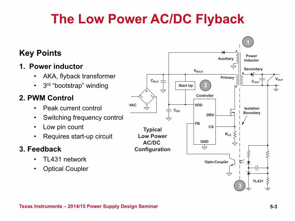
Typical
Low Power
AC/DC
Configuration
VAC
CBLK
VBULK
COUT
VOUT
CDD
RCS
Opto-Coupler
TL431
Isolation
Boundary
Start Up
Primary
AuxiliaryPower
Inductor
Secondary
Controller
GND
FB
DRV
VDD
CS
+
-
5-3 Texas Instruments – 2014/15 Power Supply Design Seminar
The Low Power AC/DC Flyback
Key Points 1. Power inductor
• AKA, flyback transformer • 3rd “bootstrap” winding
2. PWM Control • Peak current control • Switching frequency control • Low pin count • Requires start-up circuit
3. Feedback • TL431 network • Optical Coupler
1
2
3

Texas Instruments – 2014/15 Power Supply Design Seminar 5-4
The Low Power AC/DC Power Supplies
3-35 Watts, 3 V to 20 V • Universal input, 85-265 VRMS • AC/DC adapters and chargers • Set top boxes • E-meters • Auxiliary supplies – DTV, servers…
Key Parameters • Size and cost • Voltage and current control • Efficiency • Standby power
Ou
tpu
t V
olt
ag
e (
Vo
lts)
Load Current (Amps)
6
5
4
3
2
1
0
0.0 0.5 1.0 1.5 2.0 2.5
115 VAC/60 Hz 230 VAC/50 Hz
60%
65%
70%
75%
80%
85%
90%
0 10 20 30 40 50
Nameplate Power (NPP) - Watts
DOE Avg , July 2013
DOE LV Avg , July 2013
COC T2 Avg , Jan 2016
COC T2 LV Avg , Jan 2016
COC T2 10% NPP , Jan 2016
COC T2 LV 10% NPP , Jan 2016
5-5 Texas Instruments – 2014/15 Power Supply Design Seminar
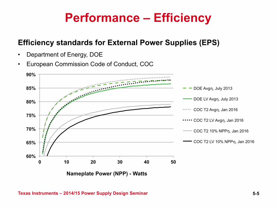
Performance – Efficiency
Efficiency standards for External Power Supplies (EPS) • Department of Energy, DOE • European Commission Code of Conduct, COC

5-6 Texas Instruments – 2014/15 Power Supply Design Seminar
Performance – Standby Power
Efficiency standards for External Power Supplies (EPS) • European Commission, Tier 2 – January 2016 75 mW • Department of Energy – July 2013 100 mW • 5 Star Charger 30 mW
• OEM specifications at 10 mW and asking for 5 mW

5-7 Texas Instruments – 2014/15 Power Supply Design Seminar
Discontinuous Current Mode (DCM)
• Single switch control • TON:
– Switch on-time – Energy taken from VIN and
stored in primary – Core is “magnetized”
• TDM: – Switch is off – Stored energy is fully
transferred to VOUT
– Core is “demagnetized” • TDIS:
– Discontinuous time – Currents are zero – TDIS = 0 à transition mode
++ VOUT
TSW = 1/fSW
TDM TDISTON
IPRI
IPRIIPRI(peak)
0
0
VIN
++ VOUTVIN
++ VOUT
ISEC
ISEC
VIN
Control
Primary Secondary
SW
SW
LP, NP NS
Basic Flyback Toplogy
Closed
Open
Energy Storage
Energy Transfer
NS
NP
NP
NS
NP
NS
VOUT + VDFWD
-VIN x
VIN +(VOUT + VDFWD) x
IPRI x
5-8 Texas Instruments – 2014/15 Power Supply Design Seminar
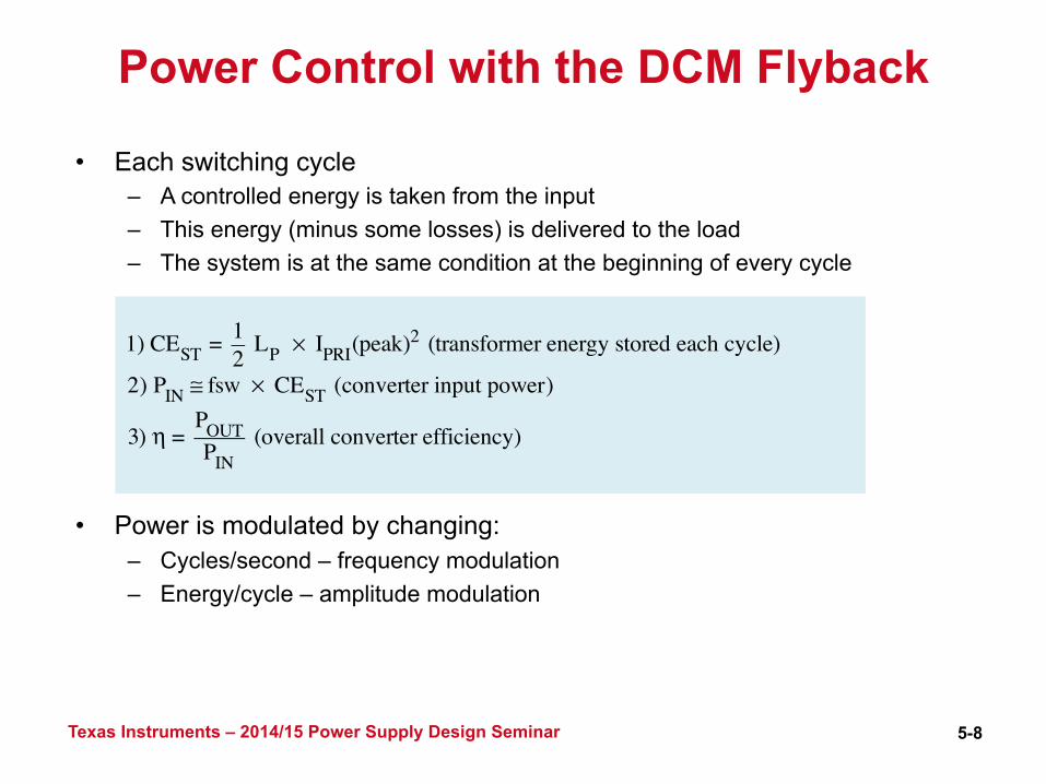
Power Control with the DCM Flyback
• Each switching cycle – A controlled energy is taken from the input – This energy (minus some losses) is delivered to the load – The system is at the same condition at the beginning of every cycle
• Power is modulated by changing: – Cycles/second – frequency modulation – Energy/cycle – amplitude modulation
1) CEST = 12 LP × IPRI(peak)2 (transformer energy stored each cycle)
2) PIN ≅ fsw × CEST (converter input power)
3) η = POUTPIN
(overall converter efficiency)

5-9 Texas Instruments – 2014/15 Power Supply Design Seminar
DCM or TM(Transition Mode) with Valley Switching
• Waiting for a zero crossing prevents continuous conduction mode (CCM)
• Switching on a valley reduces dissipation and EMI
• 1/fSW(limit) sets a minimum period
DCM-TM – Quasi-Resonant DCM – Valley Switching
TR
VBLK
Deep DCM
Drain Voltage
1/fSW(limit)

5-10 Texas Instruments – 2014/15 Power Supply Design Seminar
DCM, Fixed Frequency Control
• Frequency is constant
• Peak current is modulated
+ Controlled switching frequency - Lower efficiency - High stand-by power - Limited dynamic range
Control Law ProfileFixed Frequency
Current Mode Control
I PP
(Pea
k Pr
imar
yC
urre
nt)
I PP
– %
of M
axim
um
IPP (max)
IPP (min)
IPP
fSW (set)
f SW
f SW
– k
Hz
fSW and IPP ResponseFixed Frequency, 10 W at 5 V
DCM, LP = 750 µH
Control Voltage – VCL
Percent of Full Output Power
11010090807060504030
0% 20% 40% 60% 80% 100%
100%
80%
60%
40%
20%
0%
fSW (DCM) IPP (DCM)

5-11 Texas Instruments – 2014/15 Power Supply Design Seminar
DCM, Variable Frequency Control
• Peak current is modulated
• Frequency is modulated
• Approaches TM at low line full load
+ Smallest inductance
+ Good efficiency + Best current control
- Wide frequency range
Control Law ProfileDCM Mode
I PP
I PP
– %
of M
axim
um
IPP (max)
IPP (min)
IPP
fSW (limit)
fSW (max)
fSW (mid)
fSW (min)
f SW
(lim
it)f S
W –
kH
z
fSW and IPP Responsewith DCM Control
LP = 750 µH, 10 W at 5 V
Control Voltage – VCL
Percent of Full Output Power
100
80
60
40
20
00% 20% 40% 60% 80% 100%
100%
80%
60%
40%
20%
fSW IPP/IPP (max)

Control Law ProfileQR Mode
I PP
I PP
– %
of M
axim
um
IPP (max)
IPP (min)
IPP (mid)
IPP
fSW (limit)
fSW (max)
fSW (min)
f SW
(lim
it)
f SW
– k
Hz
fSW and IPP Responsewith TM/DCM Control
LP = 1.7 mH, 10 W at 5 V
Control Voltage – VCL
Burst
Percent of Full Output Power
140125
11958065503520
0% 20% 40% 60% 80% 100%
100%
80%
60%
40%
20%
fSW (110)IPP/IPP(max)(220)fSW (220)
IPP/IPP(max)(110)
5-12 Texas Instruments – 2014/15 Power Supply Design Seminar
TM/DCM, Variable Frequency Control
• Peak current is modulated
• Frequency is modulated
• Operates TM at full load
+ Better full load efficiency - Larger primary inductance - Wide frequency range - Reduced input voltage rejection
5-13 Texas Instruments – 2014/15 Power Supply Design Seminar
Primary Side Regulation (PSR)
Constant Voltage (CV) and Constant Current (CC) Methods

5-14 Texas Instruments – 2014/15 Power Supply Design Seminar
Primary Side Regulation (PSR)
• Controlling output voltage and current with no direct sensing
• Constant Voltage (CV) for IO = 0 A to IOCC
• Constant Current (CC) for VO = VOHU to VOCV
• The output hold up voltage, VOHU, depends on the primary controller supply dropout
VOCV
VOHU
Out
put V
olta
geOutput Current IOCC0

TL431
VAC VAC
COUT COUT VOUT
RCSRCS RF4
CC1
RF3RF2
RF1
VOUT NP
NA RS1
RS2
CB2CB1CB2CB1
CDDRS1
RS2
RF6
CDD
NS
AuxiliaryAuxiliary
Primary SecondaryPrimary Secondary
Controller
GND
VS DRV
VDD HV
CS
Controller
GND
VS DRV
VDD HV
CS
+
-+
-
5-15 Texas Instruments – 2014/15 Power Supply Design Seminar
PSR – Component Reduction
• Opto-coupler and TL431 circuits are eliminated • Less parts = lower cost, smaller supply, higher reliability • Less design, also less design flexibility
From This To This
COUT
RCS
VOUTNP NS
VBULK
RS1NA
TON
TON = the switch ON timeTDM = the transformer demagnetization timeTDIS = the discontinuous current time
TDM TDIS
Auxiliary
Primary Secondary
Controller
GND
VS DRV
VDD HV
CS
5
2
4
1
3
NA
NS
NA
NP
0 V
Auxiliary winding voltage
(VOUT + VD) x
– (VBLK ) x
5-16 Texas Instruments – 2014/15 Power Supply Design Seminar
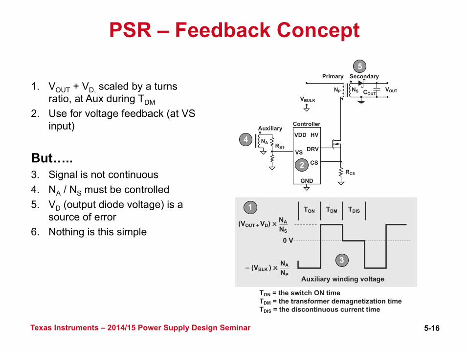
PSR – Feedback Concept
1. VOUT + VD, scaled by a turns ratio, at Aux during TDM
2. Use for voltage feedback (at VS input)
But….. 3. Signal is not continuous 4. NA / NS must be controlled 5. VD (output diode voltage) is a
source of error 6. Nothing is this simple

5-17 Texas Instruments – 2014/15 Power Supply Design Seminar
PSR – Feedback Concept
Auxiliary winding waveform: Leakage inductance
– Reset spike – Rings with CSWN
1. ESR –
2. CSWN rings with LP
Best regulation if sampled when ISEC goes to zero à “VS sample”
ISEC × RESR slope
COUT
RCS
CSWN
VOUTNP NSVBULK
RS1
RS2
NA
TON TDM TDIS
Auxiliary
Primary Secondary
Controller
GND
VS DRVSnubberClamp
EquivalentSeries Resistance
(ESR)LeakageInductance
VDD HV
CS
13
2
NA
NA
NS
NP
0 V
VS Sample
(VOUT + VD + ISECRESR) x
– (VBLK ) x Auxiliary winding voltage
5-18 Texas Instruments – 2014/15 Power Supply Design Seminar
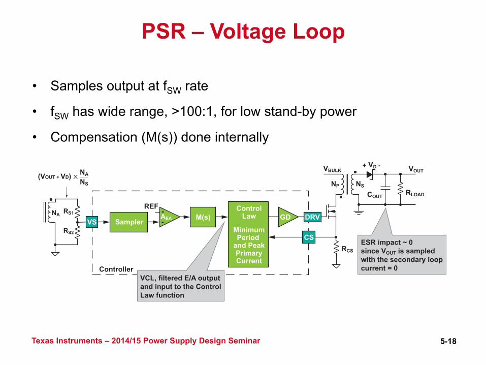
PSR – Voltage Loop
• Samples output at fSW rate
• fSW has wide range, >100:1, for low stand-by power
• Compensation (M(s)) done internally
+
+ -
ESR impact ~ 0
since VOUT is sampled
with the secondary loop
current = 0
VCL, filtered E/A output
and input to the Control
Law function
VOUT
COUT
VD
NP
VBULK
RCS
NS
RLOAD
-AEA
RS2
RS1NA
REF
Sampler
Controller
M(s)
(VOUT + VD) x NA
NS
Control
Law
Minimum
Period
and Peak
Primary
Current
GD
CS
DRVVS

5-19 Texas Instruments – 2014/15 Power Supply Design Seminar
PSR – Transient Response Problem
Poor Transient Response from Zero Load 1. Low switching
frequencies
2. Feedback is only available during a switching event
3. Poor transient performance, or a very large output capacitor
ΔVOUT =
IOUT(step)COUT × fSW(min)
As Bad as:
21
3¨VOUTVOUT
VAUX
IOUT(step)IOUT
fSW(min)
1

5-20 Texas Instruments – 2014/15 Power Supply Design Seminar
PSR Voltage Error Sources • Reference, Error Amplifier, Resistors
• Rectifier Diode Drop – Actually regulating VOUT + VD
– Diode-to-diode VD at a fixed low current is consistent for a given diode selection
– Diode temperature variation will impact VOUT if not compensated for
• Transformer – Reasonable manufacturing gives good turn control – Impact of leakage inductance is small
• Winding Voltage Sampling Errors (generally seen at light loads) – Auxiliary diode, snubber diode, snubber noise corrupting signal – Auxiliary to secondary cross-regulation at light loads – VS filtering
• Generally +/- 5% is readily achievable across line and load

5-21 Texas Instruments – 2014/15 Power Supply Design Seminar
Constant Current Control – Concept
1) IO = ISEC(Avg) =ISEC(peak)
2 ×
TDMTSW
2) ISEC(peak) = IPRI(peak) × NPNS
Therefore: 3) IO =IPRI(peak)
2 ×
NPNS
× TDMTSW
• Controlling the peak primary current and the demagnetization duty-cycle (TDM / TSW) will regulate the output current accurately
(~+/-5% achievable)
0
0
TON TDM
TSW
NS
NP
IPRI (peak)IPRI
ISEC
IPRI (peak) x

5-22 Texas Instruments – 2014/15 Power Supply Design Seminar
Standby Power (PSB)
Power consumed with zero external load, a very common state for power supplies

5-23 Texas Instruments – 2014/15 Power Supply Design Seminar
PSB = fSW(sb) × CEIN(min) + PSTRT + PLKG
Where:
fSW(sb)= converter switching frequency during stand-by
CEIN(min) = converter minimum input cycle energy
PSTRT =Start-up power
PLKG = Capacitor and junction leakage losses∑
PSB Components
• Generally fSW x CEIN dominates – Encompasses output preload and primary bias power
• PSTRT can be significant at low target PSB

VVDD
PWM Enable
VAC Applied
UVLO (on)
UVLO (off) Controller
Controller
Start-UpCurrent
HV
VDD
GND
VDD
GND
SupplyControl
PWMControl
SupplyControl
PWMControl
VAUX
VBLK
CDD
VAUX
VBLK
RSTR
CDD
NSVAUX level during TDM = (VO + VD) x NA
5-24 Texas Instruments – 2014/15 Power Supply Design Seminar
PSB – Start-Up
Active Start-Up: No PSB penalty
Resistive Start-Up:7-300 mW to PSB

5-25 Texas Instruments – 2014/15 Power Supply Design Seminar
PSB Control Law Must Haves
• Low input energy / cycle • Low switching frequency • Constant time / cycle
– Burst mode versus constant fSW(sb) – Same average cycles / second – worse transient response
Switching Cycle During Standby
Burst
Constant fSW
Same PSB but worsetransient response

5-26 Texas Instruments – 2014/15 Power Supply Design Seminar
PSB and CEIN(min)
• The minimum cycle energy is dependent on the AM range and fSW(max)
• The maximum AM range, KAM, will typically be limited to 3-5 • This expression does not take into account the impact of the
switch-node capacitance • ηT is an efficiency estimate ignoring capacitive and bias loss
CEIN
(min) =PO
(max)
ηT × fSW
(@P max)
1
KAM
⎛⎝⎜
⎞⎠⎟
2
where: KAM
=IPRI
(peak,@P max)
IPRI
(peak, min)

5-27 Texas Instruments – 2014/15 Power Supply Design Seminar
• Delta input cycle energy
• A portion of this is dissipated in the switch and tank,
• A portion goes into the transformer à output,
PSB – Switch Node Capacitance Impact
ΔCEIN(cap, total)=CSWN × VBLK2
ΔCEIN(cap, dissipated)= 12 × CSWN × VBLK
2 + VR2( )
ΔCEIN(cap, out)= 12 × CSWN × VBLK
2 – VR2( )
TR+
+
+
-
Drain
VoltageVR = (VO + VD) x
VBLK
VBULK
NP NS
VD
VO
CSWN
DRV
0 V
NP
NS

5-28 Texas Instruments – 2014/15 Power Supply Design Seminar
PSB – Switch Node Capacitance Impact
Example Power Supply Parameters PO (max) 10 W
fSW (max) 100 kHz
VBLK (max) 365 V
VR (nom) 80 V
KAM 4
CSWN 70 pF
ηT* 80%
For the example to the right ignoring the effect of CSWN:
* Efficiency estimate ignoring capacitive and bias loss
CEOUT(min) = ηT × CEIN(min) = 6.25 µJ
Total minimum energy w/ CSWN: Limits very light load efficiency and dictates a minimum load
CEIN(min) = 7.81 µJ
ΔCEIN(cap, total) = 9.33 µJ
ΔCEIN(cap, dissipated) = 4.89 µJ
ΔCEIN(cap, out) = 4.44 µJ
ΔCEOUT(cap, out) ≅ ηT × ΔCEIN(cap, out) = 3.55 µJ
CEIN(min, total) = 7.81 µJ + 9.33 µJ = 17.14 µJ
CEOUT(min, total) = 6.25 µJ + 3.55 µJ = 9.80 µJ
Incremental energy due to CSWN:

5-29 Texas Instruments – 2014/15 Power Supply Design Seminar
PSB – Minimum Load Requirements
• The converter has a minimum load it will deliver that is equal to:
• Bias power plus a preload will adjust fSW(sb) to approach fSW(min), or exceed for improved transient response
• If the preload is not adequate then regulation will be lost with VO rising
PO
(sb, total) > fSW
(min) × PO
(@P max)
fSW
(@P max)
1
KAM
⎛⎝⎜
⎞⎠⎟
2
+ ηT × C
SWN × (V
BLK2 – V
R)2
2
⎛
⎝⎜
⎞
⎠⎟

5-30 Texas Instruments – 2014/15 Power Supply Design Seminar
PSB – Versus Transient Response
PIN
(sb, total) > fSW
(sb) × P
O(max)
ηT
× fSW
(@Pmax)1
KAM
⎛
⎝⎜⎞
⎠⎟
2
+ CSWN
× 2 VACRMS2
⎛
⎝⎜⎜
⎞
⎠⎟⎟
PIN(sb) and fSW(sb) Versus VACPOUT(sb) and Transient Delta Versus fSW(sb)
25%
20%
15%
10%
5%
0%
50
40
30
20
10
0
22
20
18
16
14
2100
1900
1700
1500
13000 1000 2000 3000 4000 5000 85 135 185 235
VAC Input – VRMSFSW(sb) – Hz
F SW
(sb)
– H
z
¨9O
UT (
0.5
A, m
ax) –
%V O
UT
P IN(s
b) –
mW
P OU
T(sb
) – m
W
5 V, 10 W ExampleCOUT = 820 µFVAC =260
5 V, 10 W ExampleAdjusting POUT(sb) = 12 mWfSW(sb) > 1 kHz
¨9OUT (0.5 A, max)% POUT(sb, total) PIN(sb, total) fSW(sb)
For: VO < 10% fSW > 1200 Hz 12 mW POUT
CSWN Impact on fSW and PSB

5-31 Texas Instruments – 2014/15 Power Supply Design Seminar
Low Power Flyback Control Recap
• Discontinuous operation with variable frequency optimizes efficiency across load
• Primary side regulation can provide good V and I regulation but transient response can suffer
• Standby power benefits from: - Low switching frequencies - Low bias and start-up overhead - Low switch-node capacitance

5-32 Texas Instruments – 2014/15 Power Supply Design Seminar
Results and Comparison
How do different controllers affect the performance of a typical power supply?

5-33 Texas Instruments – 2014/15 Power Supply Design Seminar
AC/DC 5 V / 10 W Adaptor
General Specifications: • Universal AC input : 85 V to 265 V, 50/60 Hz • 5 V output; 2 A max output current Control Methodologies Evaluated: • DCM, fixed-frequency, control with opto feedback (DCM/FF/Opto) • DCM with valley switching and PSR (DCM/VS/PSR) • DCM with valley switching and opto feedback (DCM/VS/Opto) Controlled Parameters: • All designs operate at ~100 kHz at maximum load • Same transformer, FET, diode used on all designs

5-34 Texas Instruments – 2014/15 Power Supply Design Seminar
DCM/FF/Opto Example
1. Start-up resistors increase standby power 2. Large bias cap; factors include IDD, opto current, UVLO hysteresis 3. TL431 and opto-coupler for regulation
4. Faster loop response allows smaller output caps 5. Minimum on-time requires turn-on resistor at no load operation
T1435 µH13.5:1:3(Pri: Sec: Bias)
D4
SBR10U45SP5
C61 µF
C4220 µF
+ +1 µH
L2
C5220 µF
C71 µF
5 V Output at 2 A
R50
C10
2200 pF++
+
-
~ ~
+
L1
R61.00 k
R121.00 k
U2TL431AIDBZ
C130.022 µF
R9249
R101.00 k
U3
LTV-817S
VREF
VREF
C81 µF
C322 µF
R449.9
Q1AOD3N60
D5
BAS316
D290 V
D3
R349.9
R1150 k
R2150 k
C26.8 µF
C16.8 µF
100 µHD1
F1LINE
NTRL
85 to 265 VAC Input
C9
0.01 µF
C11100 pF
R75.23 k
R87.87 k
C141000 pF
U1FB
SS
RT1
RT2
REF
VDD
OUT
GND
1
2
5 3
4
UCC2809D-2 R100
100D100
BAS316
R111.00 k
R141.00 k
R101.5
49.9R3
13.5:1:3(Pri:Sec:Bias)
D3
90 VD2
435 µHT1
C6
6.8 µFC2
6.8 µFC1D1
F1
1 µF1 µFC7
820 µFC4
820 µFC5
2200pF
C10
L1
L2
100 µH
1 µH
LINE
NTRL
3.01 R18
Q1AOD3N60
1 µFC3
U1
0.91R10
1.78 k
R1131.6 kR16
133 kR15 49.9
R4D5
BAS316
100 kR17
D4
SBR10U45SP5
+ +
5 V Output at 2 A
++
+
-
~ ~
85 to 265 VAC Input1
25
3
4
VDD
VS
CBC
GND
HV
DRV
CS
UCC28710D
5-35 Texas Instruments – 2014/15 Power Supply Design Seminar
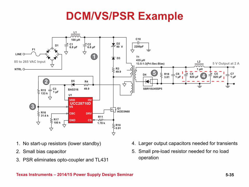
DCM/VS/PSR Example
1. No start-up resistors (lower standby) 2. Small bias capacitor
3. PSR eliminates opto-coupler and TL431
4. Larger output capacitors needed for transients 5. Small pre-load resistor needed for no load operation

T1435 µH13.5:1:3(Pri: Sec: Bias)
D4
SBR10U45SP5
C61 µF
C4220 µF
+ +1 µH
L2
C5220 µF
C71 µF
R50
C10
2200 pF++
+
-
~ ~
L1
R61.00 k
R121.00 k
U2TL431AIDBZ
C130.022 µF
R92.00 k
R102499R101
499
C1000.01 µF
U3
LTV-817S
VDD
VDD
Q1AOD3N60
U1
D290 V
D3
R349.9
C26.8 µF
C16.8 µF
100 µHD1
F1LINE
NTRL
R15133 k
R1710 k
R1630.1 k
C310 µF
U1
1
2
3
4
R111.78 k
R1430.1 k
R100.91
VDD
VS
FB
GND
HV
DRV
CS
UCC28740D
D5
BAS316
R449.9
R10310 k
5 V Output at 2 A85 to 265 VAC Input
5-36 Texas Instruments – 2014/15 Power Supply Design Seminar
DCM/VS/Opto Example
1. No start-up resistors (lower standby power) 2. Medium sized bias capacitor 3. TL431 and opto-coupler regulation
4. Faster loop response allows smaller output caps

5-37 Texas Instruments – 2014/15 Power Supply Design Seminar
Photographs
1. Start-up resistors
2. Bias capacitor
3. TL431 and opto-coupler
4. Bias capacitor
DCM/FF/Opto www.ti.com/tool/pmp9203
DCM/VS/PSR www.ti.com/tool/pmp9202
DCM/VS/Opto www.ti.com/tool/pmp9204

5-38 Texas Instruments – 2014/15 Power Supply Design Seminar
1.008
1.006
1.004
1.002
1.000
0.998
0.996
0.994
0.992
0.0 0.5 1.0 1.5 2.0 2.5
Load Currents (Amps)
Ou
tpu
t V
olt
ag
e (
No
rm
ali
ze
d)
DCM/FF/Opto DCM/VS/PSR DCM/VS/Opto
Load Regulation
• TL431 and opto-coupler provides excellent load regulation
• PSR uses cable-drop compensation - Compensates for resistive drops on the secondary side - Keeps load regulation within +/-1%

5-39 Texas Instruments – 2014/15 Power Supply Design Seminar
6
5
4
3
2
1
0
0.0 1.0 2.0 3.0 4.0 5.0 6.0 7.0
Load Currents (Amps)
Ou
tpu
t V
olt
ag
e (
Vo
lts
)
DCM/FF/Opto DCM/VS/PSR DCM/VS/Opto
Overload Protection
• Traditional fixed-frequency controller: - Frequency and peak current held constant - Currents during overload can become excessive
• DCM/VS controllers include current regulation feature
5-40 Texas Instruments – 2014/15 Power Supply Design Seminar
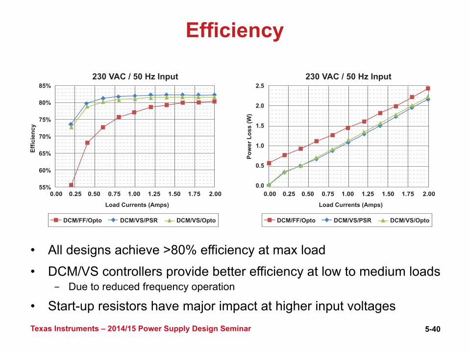
• All designs achieve >80% efficiency at max load • DCM/VS controllers provide better efficiency at low to medium loads
- Due to reduced frequency operation
• Start-up resistors have major impact at higher input voltages
Efficiency Ef
ficie
ncy
85%
80%
75%
70%
65%
60%
55%0.00 0.25 0.50 0.75 1.00 1.25 1.50 1.75 2.00
Load Currents (Amps)
DCM/FF/Opto DCM/VS/PSR DCM/VS/Opto
230 VAC / 50 Hz Input
0.00 0.25 0.50 0.75 1.00 1.25 1.50 1.75 2.00
Load Currents (Amps)
Pow
er L
oss
(W)
DCM/FF/Opto DCM/VS/PSR DCM/VS/Opto
230 VAC / 50 Hz Input2.5
2.0
1.5
1.0
0.5
0.0
5-41 Texas Instruments – 2014/15 Power Supply Design Seminar
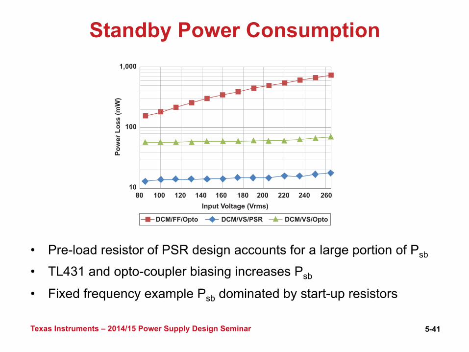
Standby Power Consumption
• Pre-load resistor of PSR design accounts for a large portion of Psb
• TL431 and opto-coupler biasing increases Psb
• Fixed frequency example Psb dominated by start-up resistors
1,000
100
10
80 100 120 140 160 180 200 220 240 260
Input Voltage (Vrms)
Po
we
r L
os
s (
mW
)
DCM/FF/Opto DCM/VS/PSR DCM/VS/Opto

5-42 Texas Instruments – 2014/15 Power Supply Design Seminar
Load Transient Response O
utp
ut
Vo
lta
ge
(A
C C
ou
ple
d,
Vo
lts
) 0.2
0.0
-0.2
-0.4
-0.6
-0.8
-1.0
-1.2
-1.0 0.0 1.0 2.0 3.0 4.0 5.0 6.0
Time (ms)
DCM/VS/PSR 0 A to 2 A DCM/VS/PSR 10 mA to 2 A DCM/FF/Opto
Ou
tpu
t V
olt
ag
e (
AC
Co
up
led
, V
olt
s) 0.2
0.0
-0.2
-0.4
-0.6
-0.8
-1.0
-1.2
-1.0 0.0 1.0 2.0 3.0 4.0 5.0 6.0
Time (ms)
• PSR response varies - Dependent on when in the switching cycle the transient hits - Starting at 0 A vs. a few mA makes a big difference
• TL431 and opto-coupler response is predictable - Dependent on output capacitance and bandwidth

5-43 Texas Instruments – 2014/15 Power Supply Design Seminar
• DCM/VS/PSR example design can be laid out to fit into a 1”x1” cube
• Two secondary transformer wires are the only electrical connection
between the two circuit boards (not possible with opto feedback)
• Small product size requires efficiency >80% to prevent thermal issues
• PMP8363 available on PowerLab: http://www.ti.com/tool/pmp8363
Small Form Factor Example

5-44 Texas Instruments – 2014/15 Power Supply Design Seminar
Comparison Summary
DCM/FF/Opto DCM/VS/PSR DCM/VS/Opto
Output Voltage Accuracy +/-2% +/-5% +/-2%
Load Regulation +/-0.1% +/-0.6% +/-0.1%
Max Load Eff. (115 VAC / 230 VAC) 82.0% / 80.4% 82.2% / 82.5% 81.3% / 81.7%
Standby Power (115 VAC / 230 VAC) 216 mW / 584 mW 14 mW / 16 mW 57 mW / 64 mW
Load Transients (0 A to 2 A) -200 mV -1100 mV -200 mV
Current Regulation Not Provided +/-5% +/-5%
# of Components 41 27 37
Relative Cost Low Lowest Low

IMPORTANT NOTICE
Texas Instruments Incorporated and its subsidiaries (TI) reserve the right to make corrections, enhancements, improvements and otherchanges to its semiconductor products and services per JESD46, latest issue, and to discontinue any product or service per JESD48, latestissue. Buyers should obtain the latest relevant information before placing orders and should verify that such information is current andcomplete. All semiconductor products (also referred to herein as “components”) are sold subject to TI’s terms and conditions of salesupplied at the time of order acknowledgment.TI warrants performance of its components to the specifications applicable at the time of sale, in accordance with the warranty in TI’s termsand conditions of sale of semiconductor products. Testing and other quality control techniques are used to the extent TI deems necessaryto support this warranty. Except where mandated by applicable law, testing of all parameters of each component is not necessarilyperformed.TI assumes no liability for applications assistance or the design of Buyers’ products. Buyers are responsible for their products andapplications using TI components. To minimize the risks associated with Buyers’ products and applications, Buyers should provideadequate design and operating safeguards.TI does not warrant or represent that any license, either express or implied, is granted under any patent right, copyright, mask work right, orother intellectual property right relating to any combination, machine, or process in which TI components or services are used. Informationpublished by TI regarding third-party products or services does not constitute a license to use such products or services or a warranty orendorsement thereof. Use of such information may require a license from a third party under the patents or other intellectual property of thethird party, or a license from TI under the patents or other intellectual property of TI.Reproduction of significant portions of TI information in TI data books or data sheets is permissible only if reproduction is without alterationand is accompanied by all associated warranties, conditions, limitations, and notices. TI is not responsible or liable for such altereddocumentation. Information of third parties may be subject to additional restrictions.Resale of TI components or services with statements different from or beyond the parameters stated by TI for that component or servicevoids all express and any implied warranties for the associated TI component or service and is an unfair and deceptive business practice.TI is not responsible or liable for any such statements.Buyer acknowledges and agrees that it is solely responsible for compliance with all legal, regulatory and safety-related requirementsconcerning its products, and any use of TI components in its applications, notwithstanding any applications-related information or supportthat may be provided by TI. Buyer represents and agrees that it has all the necessary expertise to create and implement safeguards whichanticipate dangerous consequences of failures, monitor failures and their consequences, lessen the likelihood of failures that might causeharm and take appropriate remedial actions. Buyer will fully indemnify TI and its representatives against any damages arising out of the useof any TI components in safety-critical applications.In some cases, TI components may be promoted specifically to facilitate safety-related applications. With such components, TI’s goal is tohelp enable customers to design and create their own end-product solutions that meet applicable functional safety standards andrequirements. Nonetheless, such components are subject to these terms.No TI components are authorized for use in FDA Class III (or similar life-critical medical equipment) unless authorized officers of the partieshave executed a special agreement specifically governing such use.Only those TI components which TI has specifically designated as military grade or “enhanced plastic” are designed and intended for use inmilitary/aerospace applications or environments. Buyer acknowledges and agrees that any military or aerospace use of TI componentswhich have not been so designated is solely at the Buyer's risk, and that Buyer is solely responsible for compliance with all legal andregulatory requirements in connection with such use.TI has specifically designated certain components as meeting ISO/TS16949 requirements, mainly for automotive use. In any case of use ofnon-designated products, TI will not be responsible for any failure to meet ISO/TS16949.
Products ApplicationsAudio www.ti.com/audio Automotive and Transportation www.ti.com/automotiveAmplifiers amplifier.ti.com Communications and Telecom www.ti.com/communicationsData Converters dataconverter.ti.com Computers and Peripherals www.ti.com/computersDLP® Products www.dlp.com Consumer Electronics www.ti.com/consumer-appsDSP dsp.ti.com Energy and Lighting www.ti.com/energyClocks and Timers www.ti.com/clocks Industrial www.ti.com/industrialInterface interface.ti.com Medical www.ti.com/medicalLogic logic.ti.com Security www.ti.com/securityPower Mgmt power.ti.com Space, Avionics and Defense www.ti.com/space-avionics-defenseMicrocontrollers microcontroller.ti.com Video and Imaging www.ti.com/videoRFID www.ti-rfid.comOMAP Applications Processors www.ti.com/omap TI E2E Community e2e.ti.comWireless Connectivity www.ti.com/wirelessconnectivity
Mailing Address: Texas Instruments, Post Office Box 655303, Dallas, Texas 75265Copyright © 2015, Texas Instruments Incorporated