Embed Size (px)
Citation preview

1. Introduction
1.1 Organization
1.1.1 Use of the Hyperscript
1.1.2 What it is All About
1.1.3 Relation to Other Courses
1.1.4 Books
1.1.2 Required Background Knowledge
1.1.3 Organization
1.2 Exercises and Seminar
1.2.1 General Topics
1.2.2 Rules for Seminar
1.3 Defects, Materials and Products
1.3.1 General Classification of Defects
1.3.2 Materials Properties and Defects
1.3.3 The larger View and Complications
Contents of Chapter 1
file:///L|/hyperscripts/def_en/kap_1/backbone/r1.html [02.10.2007 16:16:53]

Nobody is Perfect
1. Introduction
1.1 Organization
1.1.1 Use of the Hyperscript
There are a number of special modules that you should use for navigating through the Hyperscript:
Detailed table of contents of the main part (called "backbone")
Matrix of Modules; showing all modules in context. This is your most important "Metafile"!!!
Indexlist; with direct links to the words as they appear in the modules. All words contained in theindexlist are marked black and bold in the text.List of names; with direct links to the words as they appear in the modules. All names contained inthe name list are marked red and bold in the text.List of abbreviations; with direct links to the symbols and abbreviations as they appear in themodulesDictionary; giving the German translation of not-so-common English words; again with direct linksto the words as they appear in the modules. All words found in the dictionary are marked italic,black, and bold. The German translation appears directly on the page if you move the cursor on it
All lists are automatically generated, so errors will occur.
Note: Italics and red emphasizes something directly, without any cross reference to some list.
All numbers, chemical symbols etc. are written with bold character. There is no particular reasonfor this except that it looks better to me.Variables in formulas etc. are written in italics as it should be - except when it gets confusing. Is v av as in velocity in italics, or the greek ν? You get the point.
1.1.2 What it is All About
The lecture course "Defects in Crystals" attempts to teach all important structural aspects (as opposed toelectronic aspects) of defects in crystals. It covers all types of defects (from simple vacancies to phaseboundaries; including more complicated point defects, dislocations, stacking faults, grain boundaries),their role for properties of materials, and the analytical tools for detecting defects and measuring theirproperties
If you are not too sure about the role of defects in materials science, turn to the preface.
If you want to get an idea of what you should know and what will be offered, turn to chapter 2
A few more general remarks
The course is far to short to really cover the topic appropriately, but still overlaps somewhat withother courses. The reasons for this is that defects play a role almost everywhere in materials scienceso many courses make references to defects.
1.1.1 Introduction
file:///L|/hyperscripts/def_en/kap_1/backbone/r1_1_1.html (1 of 3) [02.10.2007 16:16:53]

The course has a special format for the exercise part similar to "Electronic Materials", but a bit lessformalized. Conventional exercises are partially abandoned in favor of "professional" presentationsincluding a paper to topics that are within the scope of the course, but will not be covered in regularclass. A list of topics is given in chapter 1.2.1
The intention with this particular format of exercises is:
Learn how to research an unfamiliar subject by yourself.
Learn how to work in a team.
Learn how to make a scientific presentation in a limited time (Some hints can be found in the link)
Learn how to write a coherent paper on a well defined subject.
Learn about a new (and hopefully exciting) topic concerning "defects".
Accordingly, the contents and the style of the presentation will also be discussed to some extent. Theemphasize, however, somewhat deviating from "Electronic Materials", is on content. For details use thelink.
1.1.3 Relation to Other Courses
The graduate course "Defects in Crystals" interacts with and draws on several other courses in thematerials science curriculum. A certain amount of overlap is unavoidable. Other courses of interest are
Introduction to Materials Science I + II ("MaWi I + II"; Prof. Föll)
Required for all "Dipl.-Ing." students; 3rd and 4th semester
Undergraduate course, where the essentials of crystals, defects in crystals, band structures,semiconductors, and properties of semiconductors up to semi-quantitave I-V-characteristics ofp-n-junctions are taught.For details of contents refer to the Hyperscripts (in german)MaWi IMaWi II
Physical Metallurgy I ("Metals I", Prof. Faupel)
Includes properties of dislocations and hardening mechanisms
Sensors I
Will, among other topics, treat point defects equilibria and reactions in the context of sensorapplications
Materials Analytics I + II ("Analytics I + II", Prof. Jäger)
Covers in detail some (but not all) of the experimental techniques, e.g. Electron Microscopy
Solid State Physics I + II ("Solid State I + II" Prof. Faupel)
Covers the essentials of solid state physics, but does not cover structural aspects of defects.
Semiconductors (Prof. Föll)
Covers "everything" about semiconductors except Si technology (but other uses of Si, somesemiconductor physics, and especially optoelectronics). Optpelectronics needs heterojunctions andheterojunctions are plagued by defects.
1.1.1 Introduction
file:///L|/hyperscripts/def_en/kap_1/backbone/r1_1_1.html (2 of 3) [02.10.2007 16:16:53]

1.1.4 Books
Consult the list of books
1.1.1 Introduction
file:///L|/hyperscripts/def_en/kap_1/backbone/r1_1_1.html (3 of 3) [02.10.2007 16:16:53]

1.1.2 Required Background Knowledge
Mathematics
Not much. Familiarity with with basic undergraduate math will suffice.
General Physics and Chemistry
Familiarity with thermodynamics (including statistical thermodynamics), basic solid state physics,and general chemistry is sufficient.
Materials Science
You should know about basic crystallography and thermodynamics. The idea is that you emergefrom this course really understanding structural aspects of defects in some detail. Since experienceteaches that abstract subjects are only understood after the second hearing, you should have heard alittle bit about point defects, dislocations, stacking faults, etc. before.
1.1.2 Required Background Knowledge
file:///L|/hyperscripts/def_en/kap_1/backbone/r1_1_2.html [02.10.2007 16:16:54]

1.1.3 Organization
Everything of interest can be found in the "Running Term" files
Index to running term
1.1.3 Organization
file:///L|/hyperscripts/def_en/kap_1/backbone/r1_1_3.html [02.10.2007 16:16:54]

1.2 Exercises and Seminar
1.2.1 General Topics
This module contains brief general information about exercises and the seminar.
Whatever is really happening in the running term, will be found in the links
Running Term●
Seminar topics●
As far as exercise classes take place, the questions will be either from the Hyperscript or will beconstructed along similar lines.As far as the seminar part is concerned: Which group will deal with which topic will be decided in thefirst week of the class.
You may choose your subject from the list of topics, or suggest a subject of your interest which isnot on the list.Presentation will be clustered at the second half of the term (or, if so demanded, in the semesterbreak); the beginning date depends on the number of participants
For most topics, you can sign out some materials to get you started; there is also always helpavailablefrom the teaching assistants.
1.2.1 Seminar and Exercises
file:///L|/hyperscripts/def_en/kap_1/backbone/r1_2_1.html [02.10.2007 16:16:54]

1.2.2 Rules for Seminar
General Rules
Teams:
Two (or, as an exception), three students form a team.
The team decides on the the detailed outline of the presentation, collects the material and writes thepaper.The delivery of the presentation can be done in any way that divides the time about equally betweenthe members of the team.Every team has an advisor who is always available (but do call ahead).
Selection of Topics and Schedules
The relevant list of topics available for the current term will be presented and discussed at the firstfew weeks of the lecture class.You may suggest your own topic.
Preparation of the Presentation
Starting material will be issued in the second week of the course, but it is the teams responsibility tofind the relevant literature.The teams should consult their advisor several weeks prior to the presentation and discuss theoutline and the contents of the presentation.
Presentation and Paper
Language
The presentation and the paper should be given in English language. Exceptions are possible upondemand; but vuegraphs must be in English without exception. Language and writing skills will notinfluence the grading.Papers must be handed in at the latest one day before the presentation in an electronic format(preferably html), and as a copy-ready paper. Very good papers written in HTML will be includedin the hyperscript.Copies for the other students will be made and issued by the lecture staff
Papers that are handed in at least one week before the presentation will be corrected with respect tolanguage (this might improve the copies you hand out!)
PresentationThe presentations must not exceed 45 min. (For exceptions, ask your advisor).
Presentations will be filmed if so desired (tell your advisor well ahead of time). The video is onlyavailable to the speakers.The presentation is followed by a discussion (10 - 15 min.) The discussion leader (usually theadvisor) may ask questions to the speaker and the audience.
1.2.2 Rules for Seminar
file:///L|/hyperscripts/def_en/kap_1/backbone/r1_2_2.html [02.10.2007 16:16:54]

1.3 Defects, Materials and Products
1.3.1 General Classification of Defects
Crystal lattice defects (defects in short) are usually classified according to their dimensions. Defects asdealt with in this course may then be classified as follows:0-dimensional defects
We have "point defects" (on occasion abbreviated PD), or, to use a better but unpopular name,"atomic size defects" .Most prominent are vacancies (V) and interstitials (i). If we mean self-interstitials (and youshould be careful with using the name interstitials indiscriminately), these two point defects (and ifyou like, small agglomerates of these defects) are the only possible intrinsic point defects inelement crystals.If we invoke extrinsic atoms, i.e. impurity atoms on lattice sites or interstitial sites, we have asecond class of point defects subdivided into interstitial or substitutional impurity atoms orextrinsic point defects. In slightly more complicated crystals we also may have mixed-up atoms (e.g. a Ga atom on an Assite in a GaAs crystal) or antisite defects
1-dimensional Defects
This includes all kinds of dislocations; for example:
Perfect dislocations, partial dislocations (always in connection with a stacking fault), dislocationloops, grain boundary and phase boundary dislocations, and evenDislocations in quasicrystals.
2-dimensional Defects
Here we have stacking faults (SF) and grain boundaries in crystals of one material or phase, and
Phase boundaries and a few special defects as e.g. boundaries between ordered domains.
3-dimensional Defects
This includes: Precipitates, usually involving impurity atoms.
Voids (little holes, i.e. agglomerates of vacancies in three-dimensional form) which may or may notbe filled with a gas, andSpecial defects, e.g. stacking fault tetrahedra and tight clusters of dislocations.
If you understand German, you will find an elementary introduction to all these topics in chapter 4 of the"Materialwissenschaft I" Hyperscript
1.3.1 General Classification of Defects
file:///L|/hyperscripts/def_en/kap_1/backbone/r1_3_1.html [02.10.2007 16:16:54]

1.3.2 Materials Properties and Defects
Material Properties and Defects
Defects determine many properties of materials (those properties that we call "structure sensitiveproperties"). Even properties like the specific resistance of semiconductors, conductance in ioniccrystals or diffusion properties in general which may appear as intrinsic properties of a material aredefect dominated - in case of doubt by the intrinsic defects. Few properties - e.g. the melting point or theelastic modulus - are not, or only weakly influenced by defects.To give some flavor of the impact of defects on properties, a few totally subjective, if not speculativepoints will follow:
Generally known are: Residual resistivity, conductivity in semiconductors, diffusion of impurityatoms, most mechanical properties around plastic deformation, optical and optoelectronicproperties, but we also have :Crystal growth, recrystallization, phase changes.
Corrosion - a particularly badly understood part of defect science.
Reliability of products, lifetimes of minority carriers in semiconductors, and lifetime of products(e.g. chips). Think of electromigration, cracks in steel, hydrogen embrittlement.Properties of quantum systems (superconductors, quantum Hall effect)
Evolution of life (defects in DNA "crystals")
A large part of the worlds technology depends on the manipulation of defects: All of the "metal bendingindustry"; including car manufacture, but also all of the semiconductor industry and many others.
Properties of Defects
Defects have many properties in themselves. We may ask for:
Structural properties: Where are the atoms relative to the perfect reference crystal?
Electronic properties: Where are the defect states in a band structure?
Chemical properties: What is the chemical potential of a defect? How does it participate inchemical reactions, e.g. in corrosion?Scattering properties: How does a defect interact with particles (phonons, photons of any energy,electrons, positrons, ...); what is the scattering cross section?Thermodynamic properties: The question for formation enthalpies and -entropies, interactionenergies, migration energies and entropies, ...
Despite intensive research, many questions are still open. There is a certain irony in the fact that pointdefects are least understood in the material where they matter most: In Silicon!
Goals of the course
This course emphasizes structural and thermodynamic properties. You should acquire:
A good understanding of defects and defect reactions.
A rough overview of important experimental tools.
Some appreciation of the elegance of mother nature to make much (you, crystals, and everythingelse) out of little (92 elements and a bunch of photons).
1.3.2 Materials Properties and Defects
file:///L|/hyperscripts/def_en/kap_1/backbone/r1_3_2.html [02.10.2007 16:16:54]

1.3.3 The larger View and Complications
Looking More Closely at Point Defects
This subchapter means to show that even the seemingly most simple defects - vacancies and interstitials- can get pretty complex in real crystals. This is already true for the most simple real crystal, the fcclattice with one atom as a base, and very true for fcc lattices with two identical atoms as a base, i.e. Si ordiamond. In really complicated crystals we have at least as many types of vacancies and interstitials asthere are different atoms - it's easy to lose perspective.
To give just two examples of real life with point defects: In the seventies and eighties a bitter warwas fought concerning the precise nature of the self-interstitial in elemental fcc crystals. The mainopponents where two large German research institutes - the dispute was never really settled.Since about 1975 we have a world-wide dispute still going on concerning the nature of the intrinsicpoint defects in Si (and pretty much all other important semiconductors). We learn from this thateven point defects are not easy to understand.
You may consider this sub-chapter as an overture to the point defect part of course: Some themestouched upon here will be be taken up in full splendor there. Now lets look at some phenomena relatedto point defectsWe start with a simple vacancy or interstitial in (fcc) crystals which exists in thermal equilibrium andask a few questions (which are mostly easily extended to other types of crystals):
The atomic structure
What is the atomic structure of point defects? This seems to be an easy question for vacancies - justremove an atom!
But how "big", how extended is the vacancy? After all, the neighboring atoms may be involved too.Nothing requires you to have only simple thoughts - lets think in a complicated way and make avacancy by removing 11 atoms and filling the void with 10 atoms - somehow. You have a vacancy.What is the structure now?How about interstitials? Lets not be unsophisticated either. Here we could fill our 11-atom-holewith 12 atoms. We now have some kind of "extended" interstitial? Does this happen? (Who knows,its possibly true in Si). How can we discriminate between "localized" and "extended" point defects?With interstitials you have several possibilities to put them in a lattice. You may choose thedumbbell configuration, i.e. you put two atoms in the space of one with some symmetry conserved,or you may put it in the octahedra or tetrahedra interstitial position. Perhaps surprisingly, there isstill one more possibility:The "crowdion", which is supposed to exist as a metastable form of interstitials at low temperaturesand which was the subject of the "war" mentioned above.Then we have the extended interstitial made following the general recipe given above, and whichis believed by some (including me) to exist at high temperatures in Si. Lets see what this looks like:
1.3.3 The larger View and Complications
file:///L|/hyperscripts/def_en/kap_1/backbone/r1_3_3.html (1 of 4) [02.10.2007 16:16:54]

Next, we may have to consider the charge state of the point defects (important in semiconductors andionic crystals).
Point defects in ionic crystals, in general, must be charged for reasons of charge neutrality. Youcannot, e.g. form Na-vacancies by removing Na+ ions without either giving the resulting vacancy apositive charge or depositing some positive charges somewhere else.In semiconductors the charge state is coupled to the energy levels introduced by a point defects, itsposition in the bandgap and the prevalent Fermi energy. If the Fermi energy changes, so does,perhaps, the charge state.
Now we might have a coupling between charge state and structure. And this may lead to an athermaldiffusion mechanisms; something really strange (after Bourgoin).
Just an arbitrary example to illustrate this: The neutral interstitial sits in the octahedra site, thepositively charged one in the tetrahedra site (see below). Whenever the charge states changes (e.g.because its energy level is close to the Fermi energy or because you irradiate the specimen withelectrons), it will jump to one of the nearest equivalent positions - in other word it diffusesindependently of the temperature.
These examples should convince you that even the most simplest of defects - point defects - are not sosimple after all. And, so far, we have (implicitly) only considered the simple case of thermalequilibrium! This leads us to the next paragraph:
But is there thermal equilibrium?
1.3.3 The larger View and Complications
file:///L|/hyperscripts/def_en/kap_1/backbone/r1_3_3.html (2 of 4) [02.10.2007 16:16:54]

The list above gives an idea what could happen. But what, actually, does happen in an ideal crystal inthermal equilibrium?
While we believe that for common fcc metal this question can be answered, it is still open for manyimportant materials, including Silicon. You may even ask: Is there thermal equilibrium at all?Consider: Right after a new portion of a growing crystal crystallized from the melt, theconcentration of point defects may have been controlled by the growth kinetics and not byequilibrium. If the system now tries to reach equilibrium, it needs sources and sinks for pointdefects to generate or dump what is required. Extremely perfect Si crystals, however, do not havethe common sources and sinks, i.e. dislocations and grain boundaries. So what happens? Not totallyclear yet. There are more open questions concerning Si; activate the link for a sample.
Well, while there may be some doubt as to the existence of thermal equilibrium now and then, there isno doubt that there are many occasions where we definitely do not have thermal equilibrium. What doesthat mean with respect to point defects?
Non-equilibrium
Global equilibrium, defined by the absolute minimum of the free enthalpy of the system is oftenunattainable; the second best solution, local equilibrium where some local minimum of the free enthalpymust suffice. You always get non-equilibrium, or just a local equilibrium, if, starting from someequilibrium, you change the temperature.
Reaching a new local equilibrium of any kind needs kinetic processes where point defects mustmove, are generated, or annihilated. A typical picture illustrating this shows a potential curve withvarious minima and maxima. A state caught in a local minima can only change to a better minimaby overcoming an energy barrier. If the temperature T does not supply sufficient thermal energykT, global equilibrium (the deepest minimum) will be reached slowly or - for all practical purposes- never.
.
One reaction helpful for reaching a minima in cases where both vacancies and interstitials exist innon-equilibrium concentrations (e.g. after lowering the temperature or during irradiationexperiments) could be the mutual annihilation of vacancies and interstitials by recombination. Thepotential barrier that must be overcome seems to be only the migration enthalpy (at least onespecies must be mobile so that the defects can meet).There might be unexpected new effects, however, with extended defects. If an localized interstitialmeets an extended vacancy, how is it supposed to recombine? There is no local empty space, just athinned out part of the lattice. Recombination is not easy then. The barrier to recombination,however, in a kinetic description, is now an entropy barrier and not the common energy barrier.
Things get really messy if the generation if point defects, too, is a non-equilibrium process - if youproduce them by crude force. There are many ways to do this:
1.3.3 The larger View and Complications
file:///L|/hyperscripts/def_en/kap_1/backbone/r1_3_3.html (3 of 4) [02.10.2007 16:16:54]

Crystal Growth As mentioned above, the incorporation of point defects in a growing interfacedoes not have to produce the equilibrium concentration of point defects. An "easy to read" paper tothis subject (in German) is available in the Link
Quenching, i.e. rapid cooling. The point defects become immobile very quickly - a lot of sinks areneeded if they are to disappear under these conditions - a rather unrealistic situation.Plastic deformation, especially by dislocation climb, is a non-equilibrium source (or sink) forpoint defects. It was (and to some extent still is) the main reason for the degradation of Laserdiodes.Irradiation with electrons (mainly for scientific reasons), ions (as in ion implantation; a keyprocess for microelectronics), neutrons (in any reactor, but also used for neutron transmutationdoping of Si), α-particles (in reactors, but also in satellites) produces copious quantities of pointdefects under "perfect" non-equilibrium conditions.Oxidation of Si injects Si interstitials into the crystal.
Nitridation of Si injects vacancies into the crystal.
Reactive Interfaces (as in the two examples above), quite generally, may inject point defects intothe participating crystals.Precipitation phenomena (always requiring a moving interface) thus may produce point defects asis indeed the case: (SiO2-precipitation generates, SiC-precipitation uses up Si-interstitials.
Diffusion of impurity atoms may produce or consume point defects beyond needing them asdiffusion vehicles.
And all of this may critically influence your product. The Si crystal growth industry, grossing some 8billion $ a year, continuously runs into severe problems caused by point defects that are not inequilibrium.
So-called swirl-defects, sub-distinguished into A-defects and B-defects caused quite someexcitement around 1980 and led the way to the acceptance of the existence of interstitials in Si.Presently, D-defects are the hot topics, and it is pretty safe to predict that we will hear of E-defectsyet.
Now, most of the examples of possible complications mentioned here are from pretty recent researchand will not be covered in detail in what follows.
And implicitely, we only discussed defects in monoatomic crystals - metals, simplesemiconductors. In more complicated crystals with two or more different atoms in the base, thingscan get really messy - look at chapters 2.4 to get an idea.
Anyway, you should have the feeling now that acquiring some knowledge about defects is notwasted time. Materials Scientists and Engineers will have to understand, use, and battle defects formany more years to come. Not only will they not go away - they are needed for many products andone of the major "buttons" to fiddle with when designing new materials
1.3.3 The larger View and Complications
file:///L|/hyperscripts/def_en/kap_1/backbone/r1_3_3.html (4 of 4) [02.10.2007 16:16:54]

2. Properties of Point Defects
2.1 Intrinsic Point Defects and Equilibrium
2.1.1 Simple Vacancies and Interstitials
2.1.2 Frenkel Defects
2.1.3 Schottky Defects
2.1.4 Mixed Point Defects
2.1.5 Essentials to Chapter 2.1: Point Defect Equilibrium
2.2 Extrinsic Point Defects and Point DefectAgglomerates
2.2.1 Impurity Atoms and Point Defects
2.2.2 Local and Global Equilibrium
2.2.3 Essentials to Chapter 2.2: Extrinsic Point Defects and Point DefectAgglomerates
2.3. Point Defects in Semiconductors like Silicon
2.3.1 General Remarks
2.4 Point Defects in Ionic Crystals
2.4.1 Motivation and Basics
2.4.2 Kröger-Vink Notation
2.4.3 Schottky Notation and Working with Notations
2.4.4 Systematics of Defect Reactions in Ionic Crystals and BrouwerDiagrams
Contents of Chapter 2
file:///L|/hyperscripts/def_en/kap_2/backbone/r2.html [02.10.2007 16:16:54]

2. Properties of Point Defects
2.1 Intrinsic Point Defects and Equilibrium
2.1.1 Simple Vacancies and Interstitials
Basic Equilibrium Considerations
We start with the most simple point defects imaginable and consider an uncharged vacancy in a simplecrystal with a base consisting of only one atomic species - that means mostly metals andsemiconductors.
Some call this kind of defect "Schottky Defect, although the original Schottky defects wereintroduced for ionic crystals containing at least two different atoms in the base.We call vacancies and their "opposites", the self-intersitals, intrinsic point defects for starters.Intrinsic simple means that these point defects can be generated in the ideal world of the idealcrystal. No external or extrinsic help or stuff is needed.
To form one vacancy at constant pressure (the usual situation), we have to add some free enthalpy GF tothe crystal, or, to use the name commonly employed by the chemical community, Gibbs energy.
GF, the free enthalpy of vacancy formation, is defined as
GF = HF – T · SF
The index F always means "formation"; HF thus is the formation enthalpy of one vacancy, SF theformation entropy of one vacancy, and T is always the absolute temperature.
The formation enthalpy HF in solids is practically indistinguishable from the formation energy EF(sometimes written UF) which has to be used if the volume and not the pressure is kept constant.
The formation entropy, which in elementary considerations of point defects usually is omitted, mustnot be confused with the entropy of mixing or configurational entropy; the entropy originating fromthe many possibilities of arranging many vacancies, but is a property of a single vacancy resultingfrom the disorder introduced into the crystal by changing the vibrational properties of theneighboring atoms (see ahead).
The next step consists of minimizing the free enthalpy G of the complete crystal with respect to thenumber nV of the vacancies, or the concentration cV = nV /N, if the number of vacancies is referred tothe number of atoms N comprising the crystal. We will drop the index "V" from now now on becausethis consideration is valid for all kinds of point defects, not just vacancies.
The number or concentration of vacancies in thermal equilibrium (which is not necessarilyidentical to chemical equilibrium!) then follows from finding the minimum of G with respect to n(or c), i.e.
∂G
∂n =
∂
∂n
G0 + G1 + G2 = 0
with G0 = Gibbs energy of the perfect crystal, G1 = Work (or energy) needed to generate nvacancies = n · GF, and G2 = – T · Sconf with Sconf = configurational entropy of n vacancies,or, to use another expression for the same quantity, the entropy of mixing n vacancies.
We note that the partial derivative of G with respect to n, which should be written as [∂G/∂n]everything
else = const. is, by definition, the chemical potential µ of the defects under consideration. This willbecome important if we consider chemical equilibrium of defects in, e.g., ionic crystals.
2.1.1 Simple Vacancies and Interstitials
file:///L|/hyperscripts/def_en/kap_2/backbone/r2_1_1.html (1 of 10) [02.10.2007 16:16:55]

The partial derivatives are easily done, we obtain
∂G0
∂n = 0
∂G1
∂n = GF
which finally leads to
∂G
∂n = GF – T ·
∂Sconf
∂n
= 0
= chemical potential in equilibrium
We now need to calculate the configurational entropy Sconf by using Boltzmann's famous formula
S = kB · ln P
With kB = k = Boltzmanns constant and P = number of different configurations (= microstates) for the samemacrostate.The exact meaning of P is sometimes a bit confusing; activate the link to see why.
A macrostate for our case is any possible combination of the number n of vacancies and the number N of atomsof the crystal. We obtain P(n) thus by looking at the number of possibilities to arrange n vacancies on N sites.
This is a standard situation in combinatorics; the number we need is given by the binomial coefficient; wehave
P =
Nn
=
N!
(N – n)! · n!
If you have problems with that, look at exercise 2.1-1 below.
The calculation of ∂S/∂n now is straight forward in principle, but analytically only possible with twoapproximations:
1. Mathematical Approximation: Use the Stirling formula in its simplest version for the factorials, i.e.
2.1.1 Simple Vacancies and Interstitials
file:///L|/hyperscripts/def_en/kap_2/backbone/r2_1_1.html (2 of 10) [02.10.2007 16:16:55]

ln x! ≈ x · ln x
2. Physical Approximation: There are always far fewer vacancies than atoms; this means
N – n ≈ N
As a first result we obtain "approximately"
T · ∂S
∂n ≈ kT · ln
N
n
If you have any doubts about this point, you should do the following exercise.
Exercise 2.1-1
Derive the Formula for cV
With n/N = cV = concentration of vacancies as defined before, we obtain the familiar formula
cV = exp –
GF
kT
or, using GF = HF – T SF
cV = expSF
k · exp –
HF
kT
For self-interstitials, exactly the same formula applies if we take the formation energy to be now theformation energy of a self-interstitial.It goes without saying (I hope) that the way you look at equations like this is via an Arrhenius plot. Inthe link you can play with that and refresh your memory
Instead of plotting cV(T) vs. T directly as in the left part of the illustration below, you plot thelogarithm lg[cV(T)] vs. 1/T as shown on the right.
2.1.1 Simple Vacancies and Interstitials
file:///L|/hyperscripts/def_en/kap_2/backbone/r2_1_1.html (3 of 10) [02.10.2007 16:16:55]

In the resulting "Arrhenius plot" or "Arrhenius diagram" you will get a straight line. The (negative)slope of this straight line is then "activation" energy of the process you are looking at (in our casethe formation energy of the vacancy), the y-axis intercept gives directly the pre-exponential factor.
Compared to simple formulas in elementary courses, the factor exp(SF/k) might be new. It will bejustified below.Obtaining this formula by shuffling all the factorials and so on is is not quite as easy as it looks - lets doa little fun exercise
Exercise 2.1-2
Find the mistake!
Like always, one can second-guess the assumptions and approximations: Are they really justified? When do theybreak down?
The reference enthalpy G0 of the perfect crystal may not be constant, but dependent on the chemicalenvironment of the crystal since it is in fact a sum over chemical potentials including all constituents thatmay undergo reactions (including defects) of the system under consideration. The concentration of oxygenvacancies in oxide crystals may, e.g., depend on the partial pressure of O2 in the atmosphere the crystalexperiences. This is one of the working principles of Ionics as used for sensors. Chapter 2.4 has more to sayto that.The simple equilibrium consideration does not concern itself with the kinetics of the generation andannihilation of vacancies and thus makes no statement about the time required to reach equilibrium. We alsomust keep in mind that the addition of the surplus atoms to external or internal surfaces, dislocations, orother defects while generating vacancies, may introduce additional energy terms.There may be more than one possibility for a vacancy to occupy a lattice site (for interstitials this is moreobvious). This can be seen as a degeneracy of the energy state, or as additional degrees of freedom for thecombinatorics needed to calculate the entropy. In general, an additional entropy term has to be introduced.Most generally we obtain
c = Zd
Z0 · exp –
GF
kT
with Zd or Z0 = partition functions of the system with and without defects, respectively. The link (inGerman) gets you to a short review of statistical thermodynamics including the partition function.
Lets look at two examples where this may be important:
The energy state of a vacancy might be "degenerate", because it is charged and has trapped an electron thathas a spin which could be either up or down - we have two, energetically identical "versions" of the vacancyand Zd/Z0 = 2 in this case.
A double vacancy in a bcc crystals has more than one way of sitting at one lattice position. There is apreferred orientation along <111>, and Zd/Z0 = 4 in this case.
2.1.1 Simple Vacancies and Interstitials
file:///L|/hyperscripts/def_en/kap_2/backbone/r2_1_1.html (4 of 10) [02.10.2007 16:16:55]

Calculation and Physical Meaning of the Formation Entropy
The formation entropy is associated with a single defect, it must not be mixed up with the entropy of mixingresulting from many defects.
It can be seen as the additional entropy or disorder added to the crystal with every additional vacancy. Thereis disorder associated with every single vacancy because the vibration modes of the atoms are disturbed bydefects.Atoms with a vacancy as a neighbour tend to vibrate with lower frequencies because some bonds, acting as"springs", are missing. These atoms are therefore less well localized than the others and thus more"unorderly" than regular atoms.
Entropy residing in lattice vibrations is nothing new, but quite important outside of defect considerations, too:
Several bcc element crystals are stable only because of the entropy inherent in their lattice vibrations. The –TS term in the free enthalpy then tends to overcompensate the higher enthalpy associated with nonclose-packed lattice structures. At high temperatures we therefore find a tendency for a phase changeconverting fcc lattices to bcc lattices which have "softer springs", lower vibration frequencies and higherentropies. For details compare Chapter 6 of Haasens book.
The calculation of the formation entropy, however, is a bit complicated. But the result of this calculation is quitesimple. Here we give only the essential steps and approximations.
First we describe the crystal as a sum of harmonic oscillators - i.e. we use the well-known harmonicapproximation. From quantum mechanics we know the energy E of an harmonic oscillator; for an oscillatornumber i and the necessary quantum number n we have
Ei,n = h ωi
2π · (n + 1/2)
We are going to derive the entropy from the all-encompassing partition function of the system and thus have tofind the correct expression.
The partition function Zi of one harmonic oscillator as defined in statistical mechanics is given by
Z i = ∑
n exp –
h ωi · (n + ½)
2π · kT
The partition function of the crystal then is given by the product of all individual partition function of the p =3N oscillators forming a crystal with N atoms, each of which has three degrees of freedom for oscillations.We have
Z =p∏
i = 1Z
i
From statistical thermodynamics we know that the free energy F (or, for solids, in a very good approximationalso the free enthalpy G) of our oscillator ensemble which we take for the crystal is given by
2.1.1 Simple Vacancies and Interstitials
file:///L|/hyperscripts/def_en/kap_2/backbone/r2_1_1.html (5 of 10) [02.10.2007 16:16:55]

F = – kT · ln Z = kT · ∑i
hωi
4πkT + ln
1 – exp –hωi
2πkT
Likewise, the entropy of the ensemble (for const. volume) is
S = – ∂F
∂T
Differentiating with respect to T yields for the entropy of our - so far - ideal crystal without defects:
S = k · ∑i
– ln 1 – exp
hωi
2π · kT
+
hωi
2π · kT
exp
hωi
2π · kT – 1
Now we consider a crystal with just one vacancy. All eigenfrequencies of all oscillators change from ωi to a newas yet undefined value ω'i. The entropy of vibration now is S'.
The formation entropy SF of our single vacancy now can be defined, it is
SF = S' – S
i.e. the difference in entropy between the perfect crystal and a crystal with one vacancy.
It is now time to get more precise about the ωi, the frequencies of vibrations. Fortunately, we know some goodapproximaitons:
At temperatures higher then the Debye temperature, which is the interesting temperature region if onewants to consider vacancies in reasonable concentrations, we have
hωi
2π << kT
hω'i
2π << kT
which means that we can expand hωi/2π into a series of which we (as usual) consider only the first term.
2.1.1 Simple Vacancies and Interstitials
file:///L|/hyperscripts/def_en/kap_2/backbone/r2_1_1.html (6 of 10) [02.10.2007 16:16:55]

Running through the arithmetic, we obtain as final result, summing over all eigenfrequencies of the crystal
SF = k · ∑i
ln ωi
ω'i
This now calls for a little exercise:
Exercise 2.1-3
Do the Math for the formula for the formation entropy
For analytical calculations we only consider next neighbors of a vacancy as contributors to the sum; i.e. weassume ω = ω´ everywhere else. In a linear approximation, we consider bonds as linear springs; missing bondschange the frequency in an easily calculated way. As a result we obtain (for all cases where our approximationsare sound):
SF (single vacancy) ≈ 0.5 k (Cu) to 1.3 k (Au).
SF (double vacancy) ≈ 1.8 k (Cu) to 2.2 k (Au).
These values, obtained by assuming that only nearest neighbors of a vacancy contribute to the formation entropy,are quite close to the measured ones. (How formation entropies are measured, will be covered in chapter 4).Reversing the argumentation, we come to a major conclusion:The formation entropy measures the spatial extension of a vacancy, or, more generally, of a zero-dimensionaldefect. The larger SF, the more extended the defect will be because than more atoms must have changed theirvibrations frequencies.
As a rule of thumb (that we justify with a little exercise below) we have:
SF ≈ 1k corresponds to a truly atomic defect, SF ≈ 10k correponds to extended defects disturbing a volumeof about 5 - 10 atoms.This is more easily visualized for interstitials than for vacancies. An "atomic" interstitials can be"constructed" by taking out one atom and filling in two atoms without changing all the other atomsappreciably. An interstitial extended over the volume of e.g. 10 atoms is formed by taking out 10 atoms andfilling in 11 atoms without giving preference in any way to one of the 11 atoms - you cannot identify a givenatom with the interstitial.
Vacancies or interstitials in elemental crystal mostly have formation entropies around 1k, i.e. they are "pointlike". There is a big exception, however: Si does not fit this picture.
While the precise values of formation enthalpies and entropies of vacancies and interstitials in Si are still notknown with any precision, the formation entropies are definitely large and probably temperature dependent;values around 6k - 15k at high temperatures are considered. Historically, this led Seeger and Chik in 1968to propose that in Si the self-interstitial is the dominating point defect and not the vacancy as in all other(known) elemental crystals. This proposal kicked of a major scientific storm; the dust has not yet settled.
Exercise 2.1-4
Calculate formation entropies
Multi Vacancies (and Multi - Interstitials by Analogy)
2.1.1 Simple Vacancies and Interstitials
file:///L|/hyperscripts/def_en/kap_2/backbone/r2_1_1.html (7 of 10) [02.10.2007 16:16:55]

So far, we assumed that there is no interaction between point defects, or that their density is so low that they"never" meet. But interactions are the rule, for vacancies they are usually attractive. This is relatively easy to seefrom basic considerations.Let's first look at metals:
A vacancy introduces a disturbance in the otherwise perfectly periodic potential which will be screened bythe free electrons, i.e. by a rearrangement of the electron density around a vacancy. The formation enthalpyof a vacancy is mostly the energy needed for this rearrangement; the elastic energy contained in thesomewhat changed atom positions is comparatively small.If you now introduce a second vacancy next to to the first one, part of the screening is already in place; thefree enthalpy needed to remove the second atom is smaller.In other word: There is a certain binding enthalpy (but from now on we will call it energy, like everybodyelse) between vacancies in metals (order of magnitude: (0,1 - 0,2) eV).
Covalently bonded crystals
The formation energy of a vacancy is mostly determined by the energy needed to "break" the bonds. Takingaway a second atom means that fewer bonds need to be broken - again there is a positive binding energy.
Ionic crystals
Vacancies are charged, this leads to Coulomb attraction between vacancies in the cation or anion sublattice,resp., and to repulsion between vacancies of the same nature. We may have positive and negative bindingenergies, and in contrast to the other cases the interaction can be long-range.
The decisive new parameter is the binding energy E2V between two vacancies. It can be defined as above, butwe also can write down a kind of "chemical" reaction equation involving the binding energy E2V (the sign ispositive for attraction):
1V + 1V ⇔ V2 + E2V
V in this case is more than an abbreviation, it is the "chemical symbol" for a vacancy.
If you have some doubts about writing down chemical reaction equation for "things" that are not atoms, youare quite right - this needs some special considerations. But rest assured, the above equation is correct, andyou can work with it exactly as with any reaction equation, i.e. apply reaction kinetics, the mass action law,etc.
Now we can do a calculation of the equilibrium concentration of Divacancies. We will do this in two ways.
First Approach: Minimize the total free enthalpy (as before):
First we define a few convenient quantities
GF(2V) = HF(2V) – TSF(2V)
HF(2V) = 2HF(1V) – E2V
SF(2V) = 2SF(1V) + ∆ S2V
With ∆ S2V = entropy of association; it is in the order of 1k - 2k in metals. We obtain in complete analogyto single vacancies
2.1.1 Simple Vacancies and Interstitials
file:///L|/hyperscripts/def_en/kap_2/backbone/r2_1_1.html (8 of 10) [02.10.2007 16:16:55]

c2V = z
2 · exp
S2V
k · exp –
HF(2V)
kT
c2V = c1V2 ·
z
2 · exp
∆S2V
k · exp
E2V
kT
The factor z/2 (z = coordination number = number of (symmetrically identical) next neighbors) takes intoaccount the different ways of aligning a divacancy on one point in the lattice as already noticed above. Wehave z = 12 for fcc, 8 for bcc and 4 for diamond lattices.
The formula tells us that the concentration of divacancies in thermal equilibrium is always much smaller than theconcentration of single vacancies since cV << 1. "Thermal equilibrium" has been emphasized, because innon-equilibrium things are totally different!
Some typical values for metals close to their melting point are
c1V = 10–4 - 10–3
c2V = 10–6 - 10–5
In the second approach, we use the mass action law.
With the reversible reaction 1V + 1V ⇔ V2V + E2V and by using the mass action law we obtain
(c1V)2
c2V
= K(T) = const · exp –∆E
kT
With ∆E = energy of the forward reaction (you have to be extremely careful with sign conventionswhenever invoking mass action laws!). This leads to
c2V = (c1V)2 · const–1 · exp
∆E
kT
In other words: Besides the "const.–1" we get the same result, but in an "easier" way.
The only (small) problem is: You have to know something additional for the determination of reactionconstants if you just use the mass action law. And that it is not necessarily easy - it involves the concept ofthe chemical potential and does not easily account for factors coming from additional freedoms oforientation. e.g. the factor z/2 in the equation above.
The important point in this context is that the reaction equation formalism also holds for non-equilibrium, e.g.during the cooling of a crystal when there are too many vacancies compared to equilibrium conditions. In thiscase we must consider local instead of global equilibrium, see chapter 2.2.3.
2.1.1 Simple Vacancies and Interstitials
file:///L|/hyperscripts/def_en/kap_2/backbone/r2_1_1.html (9 of 10) [02.10.2007 16:16:55]

There would be much more to discuss for single vacancies in simple mono-atomic crystals, e.g. how one couldcalulate the formation enthalpy, but we will now progress to the more complicated case of point defects incrystals with two different kinds of atoms in the base.
That is not only in keeping with the historical context (where this case came first), but will provide muchfood for thought.
Questionaire
Multiple Choice questions to 2.1.1
2.1.1 Simple Vacancies and Interstitials
file:///L|/hyperscripts/def_en/kap_2/backbone/r2_1_1.html (10 of 10) [02.10.2007 16:16:55]

2.1.2 Frenkel Defects
Frenkel defects are, like Schottky defects, a speciality of ionic crystals. Consult this illustration modul for pictures and more details.
In fact, the discussion of this defect in AgCl in 1926 by Frenkel more or less introduced the concepts of point defects in crystals to science.
In ionic crystals, charge neutrality requires (as we will see) that defects come in pairs with opposite charge, or at least the sum over the net charge ofall charged point defects must be zero.
"Designer defects" (defects carrying name tags) are special cases of the general point defect situation in non-elemental crystals. Since any ioniccrystal consists of at least two different kinds of atoms, at least two kinds of vacancies and interstitials are possible in principle.Thermodynamic equilibrium always allows all possible kinds of point defects simultaneously (including charged defects) with arbitraryconcentrations, but always requiring a minimal free enthalpy including the electrostatic energy components in this case.However, if there is a charge inbalance, electrostatic energy will quickly override everything else, as we will see. As a consequence we needcharge neutrality in total and in any small volume element of the crystal - we have a kind of independent boundary condition for equilibrium.Charge neutrality calls for at least two kinds of differently charged point defects. We could have more than just two kinds, of course, but again aswe will see, in real crystals usually two kinds will suffice.
One of two simple ways of maintaining charge neutrality with two different point defects is to always have a vacancy - interstitial pair, a combinationwe will call a Frenkel pair.
The generation of a Frenkel defect is easy to visualize: A lattice ion moves to an interstitial site, leaving a vacancy behind. The ion will always bethe positively charged one, i.e. a cation interstitial, because it is pretty much always smaller than the negatively charged one and thus fits betterinto the interstitial sites. In other words; its formation enthalpy will be smaller than that of a negatively charged interstitial ion. Look at thepictures to see this very clearly.
It may appear that electrostatic forces keep the interstitial and the vacancy in close proximity. While there is an attractive interaction, and closeFrenkel pairs do exist (in analogy to excitons, i.e. close electron-hole pairs in semiconductors), they will not be stable at high temperatures. If thedefects can diffuse, the interstitial and the vacancy of a Frenkel pair will go on independent random walks and thus can be anywhere, they do nothave to be close to each other after their generation.
Having vacancies and interstitials is called Frenkel disorder, it consists of Frenkel pairs or the Frenkel defects.
Frenkel disorder is an extreme case of general disorder; it is prevalent in e.g. Ag - halogen crystals like AgCl. We thus have
ni = nv = nFP
This implies, of course, that vacancies carry a charge; and that is a bit of a conceptual problems. For ions as interstitials, however, their charge isobvious. How can we understand a charge "nothing"?
Well, vacancies can be seen as charge carriers in analogy to holes in semiconductors. There a missing electron - a hole - is carrying the oppositecharge of the electron.
For a vacancy, the same reasoning applies. If a Na+ lattice ion is missing, a positive charge is missing in the volume element that contains thecorresponding vacancy. Since "missing" charges are non-entities, we have to assign a negative charge to the vacancy in the volume element to getthe charge balance right.Of course, any monoatomic crystal could (and will) have arbitrary numbers of vacancies and interstitials at the same time as intrinsic pointdefects; but only if charge consideration are important ni = nv holds exactly; otherwise the two concentrations are uncorrelated and simply givenby the formula for the equilibrium concentrations.Indeed, since the equilibrium concentrations are never exactly zero, all crystals will have vacancies and interstitials present at the same time, butsince the formation energy of interstitials is usually much larger than that of vacancies, they may be safely neglected for most considerations(with the big exception of Silicon!).
Of course, in biatomic ionic crystals, there could (and will) be two kinds of Frenkel defects: cation vacancy and cation interstitial; anion vacancy andanion interstitial; but in any given crystal one kind will always be prevalent.
We will take up all these finer points in modules to come, but now let's just look at the simple limiting case of pure Frenkel disorder.
Calculation of the Equilibrium Concentration of Frenkel Defects
Lets consider a simple ionic crystal, e.g. AgCl (being the paradigmatic crystal for Frenkel defects). With N = number of positive ions in the lattice andN' = number of interstitial sites, we obtain
N' = 2N for interstitials in the tetrahedral positionN' = 6N for the dumbbell configurationN' = .... etc.The change of the free enthalpy upon forming nFP Frenkel pairs is
∆G = nFP · HFP – nFP · TSFP – kT ·
lnN!
(N – nV)! · nV! + ln
N'!
(N' – ni)! · ni!
With HFP and SFP being the formation energy and entropy, resp., of a Frenkel pair. The configuration entropy is simply the sum of the entropyfor the vacancy and the interstitial; we wrote nV and ni to make that clear (even so we already know that nV = ni = nFP).
With the equilibrium condition ∂G/∂n = 0 we obtain for the concentration cFP of Frenkel pairs
2.1.2 Frenkel Defects
file:///L|/hyperscripts/def_en/kap_2/backbone/r2_1_2.html (1 of 2) [02.10.2007 16:16:55]

cFP = nFP
N =
N'
N
1/2 · exp
SFP
2k · exp –
HFP
2kT
The factor 1/2 in the exponent comes from equating the formation energy HFP or entropy, resp., with a pair of point defects and not with anindividual defect.
What is the reality, i.e. what kind of formation enthalpies are encountered? Surprisingly, it is not particularly easy to find measured values; the link,however, will give some numbers.That was rather straight forward, and we will not discuss Frenkel defects much more at this point. We will, however, show in the next subchapter fromfirst principles that, indeed, charge neutrality has to be maintained.
Questionaire
Multiple Choice questions to 2.1.2
2.1.2 Frenkel Defects
file:///L|/hyperscripts/def_en/kap_2/backbone/r2_1_2.html (2 of 2) [02.10.2007 16:16:55]

2.1.3 Schottky Defects
Schottky- defects use the second simple possibility to maintain charge equilibrium in ionic crystals with two atoms in the base; they consist of thetwo possible types of vacancies which automatically carry opposite charge.
Look at the illustrations in the link for visualizations of Schottky defects as a well as other defects in ionic crystals.
You may call the single vacancy in metals a Schottky defect, if you like (some do), but that somehow misses the point.
As pointed out in the context of Frenkel defects, the vacancy in ionic crystal carries a net charge the same way a hole - a missing electron -carries a charge.
We have postulated, that charge neutrality must be maintained, but we have not proved it. Moreover, even for equal numbers of oppositely chargedvacancies (or Frenkel defects for that matter), charge neutrality can only be maintained on average; on a scale comparable to the average distancebetween the point defects, we must have electrical fields which only (on average) cancel each other for larger volumes.
The total formation energy therefore must contain some electrostatic energy part because we do have electrical fields around single point defects.The same is true for the interstitials in Frenkel defects or in the general case of mixed defects, and the consideration we are going to make forvacancies applies in an analogous way to interstitials, too.Moreover, the electrical field of one vacancy will be felt by other charged point defects, which means that there is also some electrostaticinteraction between vacancies, or vacancies and other charged point defects. This interaction is stronger and has a much larger range than theelastic interactions caused by the lattice deformation around a defect.
Let's look at a relatively simple example. Here we are only going through the physical argumentation, the details of the calculations are contained inthe link.
Calling the formation energy of the anion vacancy (= missing anion = positively charged vacancy) H +, the formation energy of the cation vacancyH –, and the binding energy between close pairs H B, we obtain for ∆G, the change in free enthalpy, upon introducing n+, n–, and nB anion vacancies,cation vacancies, and vacancy pairs, resp., is
∆G = ⌠⌡
⌠⌡V
⌠⌡
H + · n+(r) + H – · n–(r) + [H+ + H – – HB] · nB (r) + 1/2 ρ (r) V (r) – T Sn dx dy dz
With ρ(r) = local charge concentration, V(r) = electrical potential, Sn = entropy of mixing; r is the space vector. The usual sum is replaced by anintegral because the electrical potential is a smooth function and not strongly localized.
The number of point defects is now dependent on r. The (non-compensated) electrical charge stems from the charged vacancies, the net electricalcharge density at any point r is thus given by
ρ (r) = e ·
n+ (r ) – n– (r)
With e being the elementary charge.
The electrostatic potential follows from the charge density via the Poisson equation, we have
∆V (r) = – 1
εε0 · ρ (r)
With ε = dielectric constant of the material and ε0 = vacuum constant
For equilibrium condition, ∆G must be minimal, i.e. we have to solve the variation problem
∆G = 0
for variations of the n's. Using the conventional approximations one obtains solutions being rather obvious on hindsight:
2.1.3 Schottky-Defects
file:///L|/hyperscripts/def_en/kap_2/backbone/r2_1_3.html (1 of 3) [02.10.2007 16:16:55]

n+(r) = N · expH + – e · V (r)
kT
n–(r) = N · exp –H – + e · V (r)
kT
nB = N · z · expH + + H – – HB
kT
For uncharged vacancies (where the – eV term would not apply), this is the old result, except that now the divacancy is included.
We still must find the electrostatic potential as a function of space. It may be obtained by expressing the charge density now with the formulas for thecharged vacancy densities given above, and then solving Poissons equation. We obtain
∆V( r ) = – e · N
εε0 ·
exp – H – + e · V (r)
k T – exp –
H + – e · V (r)
k T
This is a differential equation for the electrostatic potential; the problem now is a purely mathematical one: Solving a tricky differential equation.
It is now useful to introduce a "normalized" potential v by shifting the zero point in a convenient manner, and by utilizing a useful abbreviation.We define
v := e · V(r) – 0,5(H + + H –)
kT
χ–2 := 2 · N · e2
εε0 · kT · exp –
H + + H –
kT
This gives us a simple looking differential equation for our new quantities
∆v (r) = χ 2 · sinh {v (r)}
χ–1 has the dimension of a length, it is nothing (as it will turn out) but the (hopefully) well known Debye length for our case.
The "simple" differential equation obtained above, however, still cannot be solved easily. We must resort to the usual approximations and linearize,i.e. use the approximate relation sinh v ≈ v for small v´s.
We also need some boundary conditions as always woth differential equations. They must come from the physics of the problem.
The first guess is always to assume an infinite crystal with v = 0 for x = ± ∞. The solutions for an infinite crystal are trivial, however, wetherefore assume a crystal infinite in y- and z-direction, but with a surface in x-direction at x = 0; from there the crystal extends to infinity.Now we have a one-dimensional problem with r = x. One general solution is (please appreciate that I didn't state "obvious solution")
v(x) =
v02 –
v0'
χ
2 +
v0+ v0'
χ
2· exp [2χ · (x – x0)]
v0 + v0'
χ
· exp [χ · (x – x0)]
with v0 = v(x = 0) and v0' = integration constant which needs to be determined.
Cool, but we can do better yet:
If we do not want infinities, the divergent term exp [2χ(x – x0)] must disappear for x approaching infinity, this means
2.1.3 Schottky-Defects
file:///L|/hyperscripts/def_en/kap_2/backbone/r2_1_3.html (2 of 3) [02.10.2007 16:16:55]

limx→∞
v(x) = 0 ⇒ v0 = – v0'
χ
⇒ v(x) = 2v0 · exp – χ · x
χ–1 obviously determines at which distance from a charged surface, or more generally, from any charge, the (normalized) potential (and therefore alsothe real potential) decreases to 1/e - this is akin to the definition of the Debye length.
For a charged surface and x >> χ (i.e. the bulk of the crystal) we obtain v(x >> χ) = 0, and therefore
V(r >> χ) = H + + H –
2e
If we substitute V(r) into the equations for the equilibrium concentrations above, we obtain the final equations for the vacany concentrations in thecase of Schottky defects
n+ = n– = N · exp –H+ + H –
2kT
i.e. both concentrations are identical, and charge neutrality is maintained!
The energy costs of not doing it would be very large! That is exactly what we expected all along, except that now we proved it.
More important,however, we now can calculate what happens if there are electrical fields that do not have their origin in the vacancies themselves,but may originate from fixed charges on e.g. surfaces and interfaces (including grain boundaries or precipitates), or from the outside world.
In this case the concentrations of the defects may be quite different from the quilibrium concentrations in a neighbourhood "Debye Lenght" (= χ)from the fixed charges.We also see that we have (average) electrical neutrality in the bulk and a statistical distribution of vacancies there, but this is not necessarily truein regions within one Debye length χ next to an external or internal surface.
Charged surfaces thus may change point defect concentrations within about one Debye length. And charged point defects, if they are mobile, maycarry an electrical current or redistribute (and then changing potentials), if surface or interface charges change.This is the basic principle of using ionic conductors (and, to some extent, semiconductors) for sensor applications!
The interaction between point defects, the electrical potential and the Debye length may be demonstrated nicely by plotting the relevant curves fordifferent sets of parameters; this can be done with the following JAVA module.
We see that the Debye length as expressed in the formulas is strongly dependent on temperature. Only for high temperatures do we have enoughcharged vacancies so that their redistribution can screen a external potential on short distances. For NaCl we have, as an example, the followingvalues
T [K] χ –1 [cm]
1100 1.45 · 10 –7
900 4.55 · 10 –7
700 2.83 · 10 –6
500 8.21 · 10 –5
300 2.20 · 10 –1
The large values, however, are unrealistic in real crystals, because grain boundaries, other charged defects, and especially impurities must also beconsidered in this region; they will always decrease the Debye length.
Questionaire
Multiple Choice questions to 2.1.3
2.1.3 Schottky-Defects
file:///L|/hyperscripts/def_en/kap_2/backbone/r2_1_3.html (3 of 3) [02.10.2007 16:16:55]

2.2 Extrinsic Point Defects and Point DefectAgglomerates
2.2.1 Impurity Atoms and Point Defects
Consider a real crystal - take even a hyperpure single crystalline Si crystal if you like. It's not perfect! Itjust is not. It will always contain some impurities. If the impurity concentration is below the ppm level,then you will have ppb, or ppt or ppqt (figure that out!), or... - it's just never going to be zero.
The highest vacancy concentration your are going to have in simple metals close to the meltingpoint is around 10–4 = 100 ppm; in Si it will be far lower. On the other hand, even in the best Siyou will have some ppm of Oi (oxygen interstitials) and Ci(Carbon substitutionals).
In other words - it is quite likely that besides your intrinsic equilibrium point defects (usuallyvacancies) squirming around in equilibrium concentration, you also have comparableconcentrations of various extrinsic non-equilibrium point defects. So the question obviously is:what is going to happen between the vacancies and the "dirt"? How do intrinsic and extrinsic pointdefects interact?
Let's look at the impurities first. Essentially, we are talking phase diagrams here. If you know the phasediagram, you know what happens if you put increasing amounts of an impurity atom in your crystal.Turned around: If you know what your impurity "does", you actually can construct a phase diagram.
However, using the word "impurity" instead of "alloy" implies that we are talking about smallamounts of B in crystal A.
The decisive parameter is the solubility of the impurity atom as a function of temperature.
In a first approximation, the equilibrium concentration of impurity atoms is given by the usualArrhenius representation, akin to the case of vacancies or self-interstitials. This is often only agood approximation below the eutectic temperature (if there is one). Instead of the formationenergies and entropies, you resort to solubility energies and entropies.There is a big difference with intrinsic point defects, however. The concentration of impurity atomsin a given crystal is pretty much constant and not a quantity that can find its equilibrium value.After all, you can neither easily form nor destroy impurity atoms contained in a crystal.That means that thermal equilibrium is only obtained at one specific temperature, if at all. For allother temperatures, impurity atoms are either undersaturated or oversaturated.
Now the obvious: Vacancies, divacancies, interstitials etc. may interact with impurity atoms to formcomplexes - provided that there is some attractive interaction. Interactions may be elastic (e.g. the latticedeformation of a big impurity interstitial will attract vacancies) or electrostatic if the point defects arecharged. Schematically it may look like this:
2.2.1 Extrinsic Point Defects and Agglomerates
file:///L|/hyperscripts/def_en/kap_2/backbone/r2_2_1.html (1 of 3) [02.10.2007 16:16:55]

A impurity - vacancy complex (also known as Johnson complex) is similar to a divacancy, just oneof the partners is now an impurity atom. The calculation of the equilibrium concentration ofimpurity - vacancy complexes thus proceeds in analogy to the calculations for double vacancies, butit is somewhat more involved. We obtain (for details use the link).
cC = z · cF · cV(T)
1 – z · cF · exp
∆SC
k · exp
HC
kT
With cC = concentration of vacancy-impurity atom complexes, cF = concentration of impurityatoms, cV = equilibrium concentration of (single) vacancies, and ∆SC or HC = binding entropy orenthalpy, resp., of the pair. z, again, is the coordination number.
That the coordination number z appears in the equation above is not surprising - after all there arealways z possibilities to form one complex. Note that the term 1 – z · cF must be some correctionfactor, obviously accounting for the possible case of rather large impurity concentrations cF. Why?- Well, for small cF, this term is just about 1!
Note also that as far as equilibrium goes, we have a kind of mixed case here. The impurity atomshave some concentration cF that is not an equilibrium concentration. But if we redefine equilibriumas the state of crystal plus impurities (essentially we simply change the G0 = Gibbs energy of the"perfect" crystal in one of our first equations), than the concentration concentration cC ofvacancy-impurity atom complexes is an equilibrium concentration.
The equation above for cC is quite similar to what we had for the divacancy concentration.
If you forget the "correction factor" for a moment, we have identical exponential terms describingthe binding enthalpy, and pre-exponential factors of z · cV · cF for divacancies and z · cV · cV for thevacancy - impurity complexes.In both cases the concentrations decreases exponentially with temperature. However, assumingidentical binding enthalpies for the sake of the argument, in an Arrhenius plot the slope fordivacancies would be twice that of vacancy-impurity complexes - I sincerely hope that you can seewhy!
2.2.1 Extrinsic Point Defects and Agglomerates
file:///L|/hyperscripts/def_en/kap_2/backbone/r2_2_1.html (2 of 3) [02.10.2007 16:16:55]

The total vacancy concentration c1V(total) (= concentration of isolated vacancies + concentration ofvacancies in the complexes) as opposed to the equilibrium concentration without impurities c1V(eq) isgiven by
cV(total) = cV(eq) + cC
That's what equilbrium means! If impurity atoms snatch away some vacancies that the crystal"made" in order to be in equilibrium, it just will make some more until equilibrium is restored.cC thus can be seen as a correction term to the case of the perfect (impurity free) crystal whichdescribes the perturbation by impurities. This implies that cV >> cC under normal circumstances.
We will find out if this is true and more about vacancy - impurity complexes in an exercise.
You don't have to do it all yourself; but at least look at it - it's worth it.
Exercise 2.2-1
Properties of Johnson complexes
Questionaire
Multiple Choice questions to 2.2.1
2.2.1 Extrinsic Point Defects and Agglomerates
file:///L|/hyperscripts/def_en/kap_2/backbone/r2_2_1.html (3 of 3) [02.10.2007 16:16:55]

2.2.2 Local and Global Equilibrium
Global thermal equilibrium at arbitrary temperatures, i.e. the absolute minimum of the free enthalpy,can only be achieved if there are mechanisms for the generation and annihilation of point defects.
There must be sources and sinks for vacancies and (intrinsic) interstitials that operate with smallactivation energies - otherwise it will take a long time before global equilibrium will be achieved.
At this point it is essential to appreciate that an ideal perfect (= infinitely large) crystal has no sourcesand sinks - it can never be in thermal equilibrium. An atom, for example, cannot simply disappearleaving a vacancy behind and then miraculously appear at the surface, as we assumed in equilibriumthermodynamics, where it does not matter how a state is reached.
On the other hand, infinitely large perfect crystals do not exist - but semiconductor-gradedislocation-free single Si crystals with diameters of 300 mm and beyond, and lengths of up to 1 mare coming reasonably close. They form a special case as far as point defects are concerned.Otherwise we need other defects - grain boundaries, dislocations, precipitates and so on as sourcesand sinks for point defects. And that is what we almost always have in regular metals or ceramics.
How a grain boundary can act as source or sink for vacancies is schematically shown in the picturesbelow.
It is clear form these drawings that the activation energy (which is not the formation energy of avacancy!!) needed to emit (not to form from scratch!) a vacancy from a grain boundary is small.
Grain boundary absorbs 1 vacancy, i.e. actsas sink for one more jump of the proper
atom.
Grain boundary emits 3 vacancies, i.e. actsas source for one more jump of the 3
proper atoms.
The red arrows indicate the jumps of individual atoms. The flux of the vacancies is alwaysopposite to the flux of diffusing atoms.
We thus may expect that at sufficiently high temperatures (meaning temperatures large enough to allowdiffusion), we will be able to establish global point defect equilibrium in a real (= non-ideal) crystal, butnot really global crystal equilibrium, because a crystal with dislocations and grain boundaries is never atequilibrium.Sources and sinks are a thus a necessary, but not a sufficient ingredient for point defect equilibrium. Wealso must require that the point defects are able to move, there must be some diffusion - or you mustresign yourself to waiting for a long time.
2.2.2 Local and Global Equilibrium
file:///L|/hyperscripts/def_en/kap_2/backbone/r2_2_2.html (1 of 3) [02.10.2007 16:16:55]

At low temperatures, when all diffusion effectively stops, nothing goes anymore. Equilibrium isunreachable. For many practical cases however, this is of no consequence. At temperatures wherediffusion gets sluggish, the equilibrium concentration ceq is so low, that you cannot measure it. Forall practical purposes it surely doesn't matter if you really achieve, for example, ceq = 10–14, or ifyou have non-equilibrium with the actual concentration c a thousand times larger than ceq (i.e. c =10–11). For all practical purposes we have simply c = 0.At high temperatures, when diffusion is fast, point defect equilibrium will be established veryquickly in all real crystals with enough sources and sinks.
The intermediate temperatures thus are of interest. The mobility is not high enough to allow many pointdefects to reach convenient sinks, but not yet too small to find other point defects.
In other words, the average diffusion length or mean distance covered by a randomly diffusingpoint defect in the time interval considered, is smaller than the average distance between sinks, butlarger than the average distance between point defects.
Global point defect equilibrium as the best solution is thus unattainable at medium temperatures, butlocal equilibrium is now the second best choice and far preferable to a huge supersaturation of singlepoint defects slowly moving through the crystal in search of sinks.
Local equilibrium then simply refers to the state with the smallest free enthalpy taking into accountthe restraints of the system. The most simple restraint is that the total number of vacancies invacancy clusters of all sizes (from single vacancy to large "voids") is constant. This acknowledgesthat vacancies cannot be annihilated at sinks under these conditions, but still are able to cluster.
Let us illustrate this with a relevant example. Consider vacancies in a metal crystal that is cooled downafter it has been formed by casting.
As the temperature decreases, global equilibrium demands that the vacancy concentration decreasesexponentially. As long as the vacancies are very mobile, this is possible by annihilation at internalsinks.However, at somewhat lower temperatures, the vacancies are less mobile and have not enough timeto reach sinks like grain boundaries, but can still cover distances much larger than their averageseparation. This means that divacancies, trivacancies and so on can still form - up to large clustersof vacancies, either in the shape of a small hole or void, or, in a two-dimensional form, as smalldislocation loops. Until they become completely immobile, the vacancies will be able to cover adistance given by the diffusion length L (which depends, of course, on how quickly we cool down).In other words, at intermediate temperatures small vacancy clusters or agglomerates can be formed.Their maximum size is given by the number of vacancies within a volume that is more or less givenby L3 - more vacancies are simply not available for any one cluster.Obviously, what we will get depends very much on the cooling rate and the mobility or diffusivityof the vacancies. We will encounter that again; here is a link looking a bit ahead to the situationwhere we cool down as fast as we can.
It remains to find out which mix of single vacancies and vacancy clusters will have the smallest freeenthalpy, assuming that the total number of vacancies - either single or in clusters - stays constant. Thisminimum enthalpy for the specific restraint (number of vacancies = const.) and a given temperature thenwould be the local equilibrium configuration of the system.How do we calculate this? The simplest answer, once more, comes from using the the mass-action law.We already used it for deriving the equilibrium concentration of the divacancies. And we did not assumethat the vacancy concentration was in global thermal equilibrium! The mass action law is valid for anystarting concentrations of the ingredients - it simply describes the equilibrium concentrations for the setof reacting particles present. This corresponds to what we called local equilibrium here.
The reaction equation from sub-chapter 2.2.1 was 1V + 1V ⇔ V2 and in this case this is a validequation for using the mass action law. The result obtained for the concentration of divacancieswith the single vacancy concentration in global thermal equilibrium was
2.2.2 Local and Global Equilibrium
file:///L|/hyperscripts/def_en/kap_2/backbone/r2_2_2.html (2 of 3) [02.10.2007 16:16:55]

c2V = (c1V)2 · z
2 · exp
∆S2V
k · exp
B2V
kT
Don't forget that concentrations here are defined as n/N, i.e. in relative units (e.g. c = 3,5 · 10–5)and not in absolute units, e.g. c = 3,5 · 1015 cm–3.
For arbitrary clusters with n vacancies (1V + 1 V + ... + 1V ⇔ Vn) we obtain in an analogous wayfor the concentration cnV of clusters with n vacancies
cnV = (c1V)n · z
2 · exp
∆SnV
k · exp
BnV
kT
with BnV = average binding energy between vacancies in an n-cluster, and c1V = const.concentration of the vacancies (and no longer the thermal equilibrium concentration !).
The essential point now is to realize that these equations still work for local equilibrium! They nowdescribe the local equilibrium of vacancy clusters if a fixed concentration of vacancies is given. Thesituation now is totally different from global equilibrium. If we consider divacancies for example, wehave:Global equilibrium:
c2V(eq) << c1V(eq) ; and c2V(eq) rapidly decreases with decreasing temperatures since c1V(eq)decreases.
Local equilibrium:
c2V is increasing with decreasing T since c1V stays about constant, but we still have theexp+BnV/ kT term that increases with T
Whereas the concentration of clusters may still be small, they now contain most of the vacancies.
Generally speaking, it is always energetically favorable, to put the surplus vacancies in clustersinstead of keeping them in solid solution if there is no possibility to annihilate them completely. Itthus comes as no surprise that in rapidly cooled down crystals with not to many defects that can actas sinks, we will find some vacancy clusters at room temperature
It also should come as no surprise that the same is true for impurity atoms - vacancy clusters. Theequations governing this kind of point defect agglomeration are, after all, quite similar to the equationsdiscussed here.
If you now take the extreme case of a rather perfect Si single crystal (no sinks for point defects),where we do not just have vacancies at thermal equilibrium, but also some relevant concentration ofinterstitials, interstitial oxygen and substitutional carbon, you might well wonder what one will findat room temperature.Well - don't wonder! Get to work! It is not all that clear. And even if that puzzle has been solvedbefore you reach productive scientisthood, there is always GaAs, or InP, or SiC, or - well, you willfind something left to do, don't worry.
Questionaire
Multiple Choice questions to 2.1.1
2.2.2 Local and Global Equilibrium
file:///L|/hyperscripts/def_en/kap_2/backbone/r2_2_2.html (3 of 3) [02.10.2007 16:16:55]

2.3. Point Defects in Semiconductors like Silicon
2.3.1 General Remarks
In all semiconductors, lattice defects change the electronic properties of the material locally, and thismay result in electronic energy states in the band gap of the semiconductor and this is true for all kindsof lattice defects
Semiconductor technology actually depends completely on this fact. Doping a semiconductor, afterall, mostly means the incorporation of (usually) substitutional extrinsic point defects in definedconcentrations in defined regions of the crystal - we have B, As and P for Si.Our extrinsic point defects now exist in two states: we have some concentration [P]0 of e.g. aneutral donor like P and some concentration [P]+ of ionized donors; and [P]0 + [P]+ = [P0], thetotal concentration of P holds at all conditions.
The concentration [P]+ is simply given by the the total concentration times the probability that theelectronic state associated with the P impurity atom is not occupied by an electron.If this electrons state is at an energy ED in the band gap, basic semiconductor physics tells us thatfor a given EF and temperature T the concentration of ionized impurity atoms is given by
[P](+ ) = [P0] · {1 – f(ED, EF; T)}
≈ [P0] · expEF – ED
kT
There is no reason whatsoever that a vacancy (or any other point defect you care to come up with)should not have a energy level (or even more than one) in the band gap of its host semiconductor. Thislevel then will be occupied or not occupied by electrons exactly like the extrinsic point defect.
If the vacancy is mobile at the temperature considered, it will diffuse around - exactly like anextrinsic mobile defect.If the temperature changes, the intrinsic point defects concentration changes to the extent that it canestablish equilibrium - in pronounced contrast to the extrinsic point defects.
It should be clear form this, that intrinsic point defects in semiconductors are not all that simple. Chargestates must be considered that depend on primary doping with extrinsic point defects and temperature. Ifthings get really messy, the intrinsic point defects change the actual doping and their mobility (ordiffusion coefficient) depends on their charge state.Looking at jus at few topics in the case of Si, we obtain a bunch of complex relations, which shall onlybe touched upon:
Once again, the equilibrium concentration of charged point defects depends on the Fermi energyEF (which is the chemical potential of the electrons). As an example, for a negatively chargedvacancy we obtain
c(V – ) = c(V) · expEF – EA
kT
With EF = Fermi energy, and EA = acceptor level of the vacancy in the band gap.
2.3.1 Point Defects in Semiconductors like Silicon
file:///L|/hyperscripts/def_en/kap_2/backbone/r2_3_1.html (1 of 2) [02.10.2007 16:16:55]

This tells us that besides the formation energies and entropies, we now also must know the energylevels of the defects in the band gap!The dependence of the concentration of arbitrarily charged point defects on the carrierconcentration (i.e. on doping) is given by
cVx(n)
cVx(ni) =
n
ni
–x
With ni, n = (intrinsic) carrier density, x = charge state of point defect.
As a Si special, we also must consider self-interstitials (which, if you remember, we always can safelyneglect for just about any other elemental crystal)
Local equilibrium between vacancies and interstitials follows this relation:
cV(loc) · ci(loc) ≈ cV(equ) · ci(equ)
Considering that carrier densities and the Fermi energy depend on the temperature, too, things obviouslyget complicated!It thus should not be a big surprise that the scientific community still has not come up with reliable, orleast undisputed numbers for the basic properties of intrinsic point defects in Si, not to mention the morecomplicated semiconductors.
But do not let yourself be deceived by this: While you might have problems coming up withnumbers for e.g. the vacancy concentration in Si at some temperature and so on, the Si crystal hasno problems whatsoever to "produce" the concentration that is just right for this condition.
Here is a relevant article that can be read as a pdf file:
The Engineering of Intrinsic Point Defects in Silicon Wafers and CrystalsR. Falster and V.V. Voronkov
2.3.1 Point Defects in Semiconductors like Silicon
file:///L|/hyperscripts/def_en/kap_2/backbone/r2_3_1.html (2 of 2) [02.10.2007 16:16:55]
2.4 Point Defects in Ionic Crystals
2.4.1 Motivation and Basics
Point defects in ionic crystals (e.g. NaCl or AgCl2) and oxides (e.g. SnO2 or ZrO2) are quite importantand put to technical uses.
Unfortunately (from the metal oriented persons point of view) the scientific community workingwith those materials has its own way for dealing with point defects, which differs in some respectsfrom the viewpoint of the metal and semiconductor community.There are historical and "cultural" reasons for this, but there are also good reasons. Essentially, indealing with more complicated crystals - and ionic materials or oxides are always more complicatedthan metals or simple semiconductors - a more chemical point of view is traditional and useful. Letus look at some important points that have to be considered in this context.
First, we look at the stoichiometry of these crystals.
Ionic crystals must consist of at least two different kinds of ions. They may then contain pointdefects in concentrations far above thermal equilibrium (as defined relative to a perfect crystal), ifthe real material is non-stoichiometric. If you imagine a single crystal of, lets say, NaCl with thecomposition Na1 - δCl and δ << 1, i.e close to, but not exactly at stoichiometry (which is what youalways would expect in reality), your only way of forming a crystal seems to be to use some pointdefects as integral part of the crystal.
You might consider, e.g., to introduce a concentration of δ vacancies on the Na lattice sites, or toput a concentration of δ Cl– ions in interstitial positions, or to mix both defect types in a ratio wherethe sum of the concentrations somehow equals δ.But now lets think again. If you consider a crystal of Na1 - δCl, you are really talking about acrystal with N atoms of negatively charged Cl–- ions and N · (1 – δ) positively charged Na+ ions,which means that the crystal would carry a net negative charge of e · δ · N and thus a dramaticallyhigh energy. No such crystal can exist - there must always be equal numbers of Na+ and Cl– ions -as long as there are no impurity atoms.
This leads us to the second point, the necessity for charge equilibrium or "zero net charge condition"considered before.
If we stay with the above example of NaCl, we are forced to conclude that a NaCl crystal would benecessarily perfectly stoichiometric - it cannot grow in any other way. However, no crystal existswithout some impurities. If, for example, some Ca atoms are to be included into an otherwiseperfectly stoichiometric NaCl crystal, they will always be doubly charged Ca++ ions, and we nowmust remove twice the number of Na+ ions to preserve charge neutrality (or introduce twice thenumber of additional Cl- ions). Obviously we now must introduce a Na vacancy for every Ca++ ionincluded in the crystal (or Cl- interstitials and so on).The concentration of vacancies now could be much higher than the thermal equilibriumconcentration. But we still may have equilibrium; namely chemical equilibrium, or, if the defectsare charged, electrochemical equilibrium!
We see with this simple example, that there is a linkage between stoichiometry, charge neutrality,impurities and defects, with the added complication that it is not necessarily clear which kinds of pointdefects must be present in what concentration.
We also see that point defects in concentrations that have nothing to do with the thermalequilibrium concentration in perfect crystals may be an integral part of a real ionic crystal.
The simple example, however, makes also clear that stoichiometry, impurity, and charge neutralityconsiderations still do not tell us exactly what kinds of point defects are needed in which concentration,but at best will give some integral numbers.Let us look at a third point. It concerns the surface and its interaction with the surroundings - this iswhere many applications come in.
2.4.1 Point Defects in Ionic Crystals
file:///L|/hyperscripts/def_en/kap_2/backbone/r2_4_1.html (1 of 2) [02.10.2007 16:16:56]

Consider a ZrO2 crystal in thermal equilibrium with a gas containing a certain O2 concentration, ata temperature where the oxygen in the crystal is mobile to some extent (maybe because there areO-vacancies?). We must expect some "chemical" reaction to take place. Some additional oxygenmay be incorporated into the crystal, or some oxygen may diffuse out of the crystal into the gas.The tendency of whatever is going to happen in this case will be determined by the conditions forchemical equilibrium, or, in other word, by the chemical potentials of the participating species.
But we must expect that point defects are involved in whatever happens across the interface. For theparticular example given (which happens to describe the principle of an oxygen sensor) we mustexpect that some electrical effects take place as well because introducing excess oxygen (alwaysnegatively charged) into the crystal or taking some out, will influence the charge distributions andthus electrical potentials in the crystal.Some electrochemical equilibrium will be reached that contains electrical potential differences - avoltage develops across the interface.
The common denominator in all considerations made so far was: We always had some kind of linkagebetween "chemistry" as expressed in reactions between atoms or in stoichiometric considerations, and(usually charged) point defects..We now get the idea of what needs to be done for a general treatment of point defects and ionic crystals:
We want to define point defects in a waywhere they can be included
into the familiar concept of chemical reaction equationsWe then treat them the same way we treat chemical reactions
In other words, we want to write equations analogous to
n · A + m · B ⇔ AnBm
[A]n · [B]n
[AnBm] = const.
With the option that "A" and "B" may refer not only to atoms, but also to point defects.
We want to do this in a way where we can use the full box of tools developed for chemical reactions,e.g. the mass action law (shown above), chemical potentials and activities instead of concentrations,the concept of kinetics, of chemical equilibrium, etc.As is turns out, this is possible, but it is not obvious how to do this right. There are several approachesand compromises to achieve the best description. We will look at this in the next subchapter.
2.4.1 Point Defects in Ionic Crystals
file:///L|/hyperscripts/def_en/kap_2/backbone/r2_4_1.html (2 of 2) [02.10.2007 16:16:56]

2.4.2 Kröger-Vink Notation
How do we treat point defects in perfect analogy to atoms and molecules in chemical reaction equations? A very clear waywas suggested by Kröger and Vink, it is therefore called "Kröger-Vink notation" or notation by "structure elements" -we already had a glimpse of this.
We define vacancies and interstitials as particles which occupy a defined site in a crystal and which may have a charge.
Sites in a crystal are the points where the atoms, the interstitials, or the vacancies can be. For a crystal composed of twokinds of atoms we have, e.g., the "A-sites" and the "B-sites". An A-atom on an A-site we denote by AA, a vacancy on aB-site is a VB
This leaves the interstitials out of the picture. We therefore simply name all possible interstitials sites with their ownplace symbol and write Ai or Bi for an A-atom or a B-atom, resp., on its appropriate interstitial site.
An interstitial site not occupied by an interstitial atom then, by definition, is occupied by a vacancy and symbolized byVi. A perfect crystal in the Kröger-Vink notation thus is full of vacancies on interstitial sites!
In order to facilitate book keeping with respect to the electrical charge, we only note the excess charge relative to the
neutral lattice. Positive excess charge is marked by a point (e.g. A·), negative charge by a hyphen or dash or whatever you
like to call it (e.g. A/) to distinguish this relative charge from the absolute charge. If we consider a positively charged Na+
ion in the NaCl lattice, we write NaNa as long as it is sitting on its regular lattice position, i.e. without a charge symbol. If wenow consider a vacancy on the Na-site, the Na-ion as interstitial, or a Ca++ ion on the Na-site, we write
V /Na, Na·
i, and Ca·Na because this defines the charge relative to the neutral lattice.
Running through all the possible combinations for our NaCl crystal with some Ca, we obtain the matrix
A atom (Na+) B atom (Cl–) Vacancy C atom (Ca++)
A-site NaNa Cl / /Na V /Na Ca ·Na
B-site Na ··ClClCl V · Cl Ca ···Cl
i-site Na ·i Cl /i Vi Ca ··i
This calls for a little exercise
Exercise 2.4.1
Describing structure elements
What have we gained by this? We now can describe all kinds of structure elements - atoms, molecules and defects - and theirreactions in a clear and unambiguous way relative to the empty space. Lets look at some examples
Formation of Frenkel defects in, e.g., AgCl:
AgAg + Vi = V /Ag + Ag ·i
We see why we need the slightly strange construction of a vacancy on an interstitial site.
Formation of Schottky defects for an AB crystal
2.4.2 Kröger-Vink Notation
file:///L|/hyperscripts/def_en/kap_2/backbone/r2_4_2.html (1 of 3) [02.10.2007 16:16:56]

AA + BB = V /A + V ·B + AA + BB
AA + BB = V /A + VB · + AB
The second equation simply considers the two dislodged atoms as a molecule that must be put somewhere.
This looks good. The question is, if we now can use the mass action law to determine equilibrium concentrations. If theFrenkel defect example could be seen as analogous to the chemical reaction A + B = AB, we could write a mass action lawas follows:
[AgAg] · [Vi]
[V /Ag] · [Agi ·]
= const
with [A] meaning "concentration of A". The reaction constant is a more or less involved function of pressure p andtemperature T, and especially the chemical potentials of the particles involved.
Unfortunately, this is wrong!
Why? Well, the notion of chemical equilibrium and thus the mass action law, at the normal conditions of constanttemperature T and pressure p, stems from finding the minimum of the free enthalpy G (also called Gibbs energy) which inour case implies the equality of all chemical potentials. You may want to read up a bit on the concept of chemical potentials,this can be done in the link.
In other words, we are searching for the equilibrium concentration of the particles ni involved in the reaction, which, ata given temperature and pressure, lead to dG = 0.The equation dG = 0 can always be written as a total differential with respect to the variables dni:
dG = ∂G
∂n1
· dn1 + ∂G
∂n2
· dn2 + ...
The partial derivatives are defined as the chemical potentials of the particles in question and we always have to keep inmind that the long version of the above equation has a subscript at every partial derivative, which we, like many others,conveniently "forgot". If written correctly the partial derivative for the particle ni reads (in HTML somewhatawkwardly),
∂G
∂ni
p, T, nj ≠ i = const
Meaning that T, p, and all other particle concentrations must be kept constant.
Only if that condition is fulfilled, a mass action equation can be formulated that involves all particles present in the reactionequation! And fulfilling the condition means that you can - at least in principle - change the concentration of any kind ofparticle (e.g. the vacancy concentration) without changing the concentration of all the other particles.
This "independence condition" is automatically not fulfilled if we have additional constraints which link some of ourparticles. And such constraints we do have in the Kröger-Vink notation, as alluded to before!
2.4.2 Kröger-Vink Notation
file:///L|/hyperscripts/def_en/kap_2/backbone/r2_4_2.html (2 of 3) [02.10.2007 16:16:56]

There is no way within the system to produce a vacancy, e.g. VA without removing an A-particle, e.g. generating an Aior adding another B-particle, BB.
S... ! We now have a very useful way of describing chemical reactions, including all kinds of charged defects, but we cannotuse simple thermodynamics! That is the point where other notations come in.You now may ask: Why not introduce a notation that has it all and be done with it?
The answer is: It could be done, but only by losing simplicity in describing reactions. And simplicity is what you needin real (research) life, when, in sharp contrast to text books, you do not know what is going on, and you try to get ananswer by mulling over various possibility in your mind, or on a sheet of paper.
So "defects-in-ceramics" people live with several kinds of notation, all having pro and cons, and, after finding a goodformulation in one notation, translate it to some other notation to get the answers required. We will provide a glimpse of thisin the next subchapter.
2.4.2 Kröger-Vink Notation
file:///L|/hyperscripts/def_en/kap_2/backbone/r2_4_2.html (3 of 3) [02.10.2007 16:16:56]

2.4.3 Schottky Notation and Working with Notations
Schottky Notation
The Kröger-Vink notation defined structure elements - atoms, molecules, point defects and even electrons and holes relative to empty space. Despitethe problem with the inapplicability of the mass action law, this notation is in use throughout the scientific community dealing with point defects.The other important notation - the "Schottky notation" or "building element notation" is defined as follows:
Defects are defined relative to the perfect crystal.
Charges are notated as in the Kröger-Vink way, i.e. relative to the perfect crystal. We again use the "·" for positive (relative) charge and the "/"for (relative) negative charge.
To make things a bit more complicated, there are two ways of writing the required symbols, the "old" and the "new" Schottky notation.
The "old" Schottky notation used special graphical symbols, like black circles or squares which are not available in HTML anyway.
So we only give the new Schottky notation in direct comparison with the Kröger-Vink notation, again for the example NaCl with Ca impurities,i.e.A = Na+, B = Cl–, C = Ca++.
A on B site A-vacancy A-interstitial
Schottky(new) Na|Cl| ·· |Na|/ Na ·
Kröger-Vink NaCl ·· VNa/ Nai ·
So far, the difference between the Schottky notation and the Kröger-Vink notation seems superficial. The important difference, however, becomesclear upon writing down defect reactions. Lets look at the formation of Frenkel and Schottky defects in the two notations.
Frenkel defects Schottky defects
Schottky(new) |Ag|/ + Ag · = 0 |Ag|/ + |Cl|· + AB = 0
Kröger-Vink AgAg + Vi = V/Ag + Ag ·i AgAg + ClCl = V/
Ag + V ·Cl + AB
In words, the Schottky notation says:
For Frenkel defects: A negatively charged Ag vacancy plus a positively charged Ag interstitial gives zero.
For Schottky defects: A neatively charged Ag vacancy plus a positively charged Cl vacancy plus a AgCl "lattice molecule" gives zero.
This is clear enough for these simple cases, but not as clear and easy as the Kröger-Vink notation.
But, and that is the big advantage, we can apply the mass action law directly to the reactions in the Schottky notation.
This is not directly obvious. After all, Frenkel defects, e.g., do not only appear to be linked (where there is an interstitial, there is also a vacancy),but actually are linked if the defects are charged (otherwise there would be neither net charge in the crystal, or we would have to invoke electronsor holes to compensate the ionic charge - but then we would have to include those into the reaction equation).Theoretically, however, you can introduce one more vacancy or one more interstitial into a crystal with a given concentration of each and look atthe change of the free enthalpy, i.e. the chemical potential of the species under consideration. The independence condition does not require that itis easy to change individual concentrations, only that it is possible!If you do neglect the energy associated with charge (i.e. you look at the chemical and not the electrochemical potential), the answers you get willnot contain the coupling between the defects and you have to consider that separately. We will see how this works later.
Now, why don't we use just the Schottky notation and forget about Kröger-Vink? We asked that question before; the answer hasn't changed: If welook at more complicated reactions, e.g. between point defects in an ionic crystal, a gas on its outside, and with electrons and holes for compensatingcharges, it is much easier to formulate possible reaction in the Kröger-Vink notation. The trick now is, to convert your reaction equations from theKröger-Vink structure elements to the Schottky building elements. There is a simple recipe for doing this.
Converting Kröger-Vink to Schottky
All we have to do, is to combine the two structure elements of Kröger-Vink that refer to the same place in the lattice and view the combination as abuilding element.Lets first look at an example and then generalize. Consider the Frenkel disorder in AgCl. Using structure elements, we write
2.4.3 Schottky Notation and Working with Notations
file:///L|/hyperscripts/def_en/kap_2/backbone/r2_4_3.html (1 of 6) [02.10.2007 16:16:56]

AgAg + Vi = V/Ag + Ag ·i
Combining the terms referring to the same place in the lattice (with the actual defects always as the first term in the combination) yields
(V/Ag – AgAg) + (Ag i – Vi) = 0
Now all we have to do is to write down the corresponding Schottky notation and identify the terms in brackets with the Schottky structureelements. We see that
(V/Ag – AgAg) = |Ag|/
(Ag ·i – Vi) = Ag ·
We can generalize this into a "translation table":
A onB site A-vacancy A-interstitial AB
moleculeC onB site
Freeelectron hole
All defects neutral Always charged
Schottky(new)
Buildingelements
A|B| |A| A AB C|B| e/ h ·
Kröger-VinkStructureelements
AB VA Ai AB CB e/ h ·
Combinedstructure
elements =Buildingelements
AB -BB
VA - AA Ai - Vi ABCB -BB
e/ h ·
The General Recipe for Point Defect Reactions and First Example
If you now stick to the full formalism, what you do is:
1. Write down the possible reaction with structure elements (= Kröger-Vink notation).
2. Translate that to building elements (= Schottky notation).
3. Consider charges and check for electroneutrality. If the sum of all charges is not zero, search for mistakes and if there are none, throw in holesor electrons, as your system provides.4. Use the mass action law with the final (building element) equation (including holes or electrons).
First Example: Schottky Defects
We take the Schottky defect as a fitting elementary example and go through the movements:
1. Kröger-Vink structure element equation
AgAg + ClCl = V/Ag + V ·Cl + AB
2.4.3 Schottky Notation and Working with Notations
file:///L|/hyperscripts/def_en/kap_2/backbone/r2_4_3.html (2 of 6) [02.10.2007 16:16:56]

After rearranging (remember, the defect comes first!) so we can use the translation table, we have
(V/Ag – AgAg) + (V · Cl – ClCl) + AB = 0
2. Switch to building elements using the the expressions in brackets; we have
|Ag|/ + |Cl| · + AB = 0
3. Charge neutrality demands
Σ(pos. charge) = Σ(neg. charge)
[|Ag|/] = [|Cl| ·]
4. The mass action law now gives
[|Ag|/] · [|Cl| ·]
[AB] = exp –
Σν i µ i0
kT€
And this leads to
[|Ag|/] = [|Cl| ·] = [AB] · exp –Σ ν i µ i
0
kT
With µ i = standard chemical potentials of the two vacancies and a lattice molecule, resp., and ν i = stoichiometric coefficients of the reaction(1,1, and – 1 in our case).
This sure looks strange compared to the formula derived in the "physical" way. But it is the same. Lets see why.
First, the activity (or concentration) of the lattice molecule AB is simply [AB] = 1 since it is nothing but the number of mols of AgCl moleculesin one mol of AgCl; i.e. it is = 1. This gives us
[|Ag|/] · [|Cl| ·] = exp –Σ ν iµ i
0
kT
Now lets look at the energies in the exponent. As always, the energy scale is relative. From whatever zero point you measure your energy tomake an Ag vacancy or a Cl vacancy, you must subtract the energy of the AB molecule as measured in that system. If you take it to be zero -which then defines the energy origin of your standard system - the standard chemical potentials of the two vacancies are just the usual formationenergies.
Note that as in treatment given before, the mass action law alone does not specify the vacancy concentration, only their product.
Only invoking the electroneutrality condition, which demands [|Ag|/] = [|Cl| ·], allows to compute the individual concentrations. Writing H+ andH– for the formation enthalpies of the positively or negatively charged vacancy, resp., we obtain the familiar result
[|Ag|/] = [|Cl| ·] = exp –H+ + H–
2kT
Second Example: Frenkel Defects
First we write down the reaction with structure elements (= Kröger-Vink notation).
2.4.3 Schottky Notation and Working with Notations
file:///L|/hyperscripts/def_en/kap_2/backbone/r2_4_3.html (3 of 6) [02.10.2007 16:16:56]

AA + Vi = Ai· + VA
/
After rearranging (remember, the defect comes first!) so we can use the translation table, we have
(Ai· – Vi) + (VA
/ – AA) = 0
2. The expressions in brackets are the building elements, we have
|A|· + |A|/ = 0
3. Charge neutrality demands
|A|· = |A|/
4. The mass action law now gives
A problem? What are we going to do with the "0"? Well, there really is no problem with the zero - just take the mass action law as it is
Π(ai)νi = exp –G0
kT = K = Reaction
Constant
Nowhere was it required that in the product there must be terms with negative stoichiometry coefficients νi. This gives us
[A·] · [|A|/] = exp –GF
kT
And we identify G0 with the formation energy GF of a Frenkel pair as before.
Together with the charge neutrality condition we have
[A·] = [|A|/] = exp –GF
2kT
almost the familiar result - except that we do not have the factor (N/N')1/2.
OK - we do have a problem, but not with the zero. Where did we lose the factor (N/N')1/2 ?
Lets look at equilibrium another way. We do not involve the mass action law but go one step back to the equilibrium condition for the chemicalpotentials: µA· = µ|A|/ . We write the chemical potentials in the standard form and obtain
µA· = µ0A· + kT · ln
nA·
N'
µ|A|/ = µ0|A|/ + kT · ln
n|A|/
N
2.4.3 Schottky Notation and Working with Notations
file:///L|/hyperscripts/def_en/kap_2/backbone/r2_4_3.html (4 of 6) [02.10.2007 16:16:56]

For equilibrium we now obtain (if you wonder at the n/N and n/N', consult the link)
nA· · n|A|/ = N · N' · exp –µ0
A· + µ0|A|/
kT
Charge neutrality tells us that
nA· = n|A|/ = nFP
For the concentration of Frenkel pairs cFP = nFP/N we now obtain the correct old formula
cFP =
N
N'
1/2 · exp –
µ0A· + µ0
2kT
=
N
N'
1/2 · exp –
GFP
2kT
Aha! Applying the mass action law uncritically causes a problem: The standard chemical potentials of vacancies and interstitials were for differentstandard conditions:
In one case (the vacancies) the standard condition was for adding N vacancies to the system, in the other case (the interstitials) it was for addingN' = N · l interstitials (and l being some factor taking into account that there are more positions for interstitials than for vacancies in a crystal).
If that appears to be incredibly complicated and prone to errors - that's because it is! But take comfort: You get used to it, and working with it isnot all that difficult after overcoming an intial "energy barrier".
Some Remarks to Practical Work
Many books and other texts to not dwell extensively on the fine differences between notations, problems with the standard condition in the chemicalpotentials, meaning of reaction equations and so on - they write down a reaction equation, in the worst case a mix of Kröger-Vink and Schottkynotations, throw in electrons or holes right away to achieve charge neutrality, and write down the mass action law in the form
Πi
(ai)νi = exp –G
kT = K(T) = const · exp –
G
kT
And not much attention is given to the constant K(T) in front of the exponential.
Even though it's faulty thermodynamics, let's see what happens if we do that for Frenkel defects in the Kröger-Vink notation:
The reaction equation was
AgAg + Vi = V/Ag + Ag ·i
AgAg + Vi – V/Ag – Ag · = 0
The mass action law uncritically applied gives
[AgAg] · [Vi]
[V/] · [Ag ·] = const · exp –
G'
kT
As long as the defect concentration is small compared to the concentrations of atoms and lattice sites, we may simply equate
2.4.3 Schottky Notation and Working with Notations
file:///L|/hyperscripts/def_en/kap_2/backbone/r2_4_3.html (5 of 6) [02.10.2007 16:16:56]

[AgAg] = 1
[Vi] = 1
Which leaves us with
[V/] · [Ag ·] = const · exp –G
kT
With G = – G', but that is irrelevant - we simply know that the exponential always has a minus sign for the reactions we are interested in and thatG must be the formation enthalpy of a Frenkel pair.
That is the correct result, expressed in Kröger-Vink terms. What that means is that you don't have to worry all that much about the finer details aslong as you are not terribly interested in the exact value of the constant in front of the exponential - you will mostly get your reaction equation right!
Luckily, there are only a few fundamental reaction equations involving point defects - everything else can be expressed as linear combinations ofthe fundamental reactions (like Frenkel and Schottky defect equilibrium) - after some initiation, you will feel quite comfortable with defectreactions.
As shown above for Frenkel defects, it is often advisable not to use the mass action law directly, but to go one step back and use the equilibriumcondition for the chemical potentials. This gives not only a clearer view of what constitutes the standard conditions, but also circumvents a number ofother problems associated with the law of mass action (if you really want to know, consult the advanced module accessible by the link).
2.4.3 Schottky Notation and Working with Notations
file:///L|/hyperscripts/def_en/kap_2/backbone/r2_4_3.html (6 of 6) [02.10.2007 16:16:56]

2.4.4 Systematics of Defect Reactions in Ionic Crystals and Brouwer Diagrams
There are essentially three fundamental situations for defects in ionic crystals.
Intrinsic defects; i.e. the defects present in the bulk of a crystal in thermodynamic equilibrium. This includesthe Frenkel and Schottky defects considered before, but also some other kinds not yet discussed.Defect Doping; i.e. the intentional manipulation of defect types and concentrations by the incorporation ofspecific impurities into the (bulk of the) crystal.Defect reactions at interfaces, e.g. the incorporation of atoms or molecules from the "outside" into thecrystal via defects - or the opposite, the loss of crystal atoms to the outside world generating defects in thecrystal.
There are not always clear distinctions, but lets look at these three cases separately for a start.
Intrinsic Defects in Ionic Crystals
This case includes all defect situations that one could find in a perfect ionic crystal. Besides Schottky and Frenkeldisorder or any mixture of the two, we could have many more defects - any combination of interstitials andvacancies for any kind of atom in the crystal is admissible.
One example: In an AB crystal, instead if two oppositely charged vacancies (the Schottky defects), we couldalso have two interstitials of the two kinds of atoms carrying different charge.This kind of defect is called an "Anti Schottky defect", it would be formed according to the (Kröger-Vink)reaction
AB + 2Vi = Ai· + Bi
/
Following our recipe, we obtain after rearranging and "translating" to Schottky notation:
(Ai· – Vi) + (Bi
/ – Vi) = AB
A· + B/ = AB
This is essentially the same result as for the regular Schottky defects. However, in using the mass action law, wewould have to use the formation energies for interstitials (and take care of the additional degrees of freedom forarranging interstitials as in the case of Frenkel defects).
In reality, the formation energies of interstitials are mostly larger than those for vacancies; this is certainlytrue for the "big" negatively charged anion interstitial.Anti Schottky defects therefore have not been observed as the dominating defect type so far. But they are notonly perfectly feasible, but also always present - only their concentration is so small that it can not bemeasured; consequently they do not play a role in anything interesting connected with defects.
We could also conceive of "anti site defects", i.e. A-atoms on B-places and vice versa; AB and BA, ofcombinations like a VA and AB, and of plenty more intrinsic defects for more complicated crystals, e.g. forYBa2Cu3O7 (the famous first high temperature superconductor with a critical temperature larger than the boilingpoint of liquid N2).
We could, moreover, include isoelectronic impurity atoms into the list; e.g. K instead of Na; Ba instead ofCa, or F instead of Cl, which could be incorporated into a crystal without the need to change anything else.A little dirt, after all, is always "intrinsic", too.And all the reactions that are conceivable will occur. The only difference is that some might be frequent andsome might be rare - and it is often sufficient to only consider the dominating reaction.
This teaches us a major lesson, especially with respect to the upcoming paragraphs
2.4.4 Defect Reactions in Ionic Crystals
file:///L|/hyperscripts/def_en/kap_2/backbone/r2_4_4.html (1 of 10) [02.10.2007 16:16:56]

There are far too many defect types and reactions principally possible in simple (ionic) crystals (not tomention complicated ones) for a priori treatments of all possible effects. We must invoke some additionalinformation (such as anion interstitials being unlikely) to simplify the situation to a level where it can behandled.For the intrinsic defects mentioned so far, this was easy and has been done all along. It will become animportant guiding principle for the other two cases, however.
But we are not yet done with intrinsic defects: If we look at semiconducting ionic or compound crystals, we mayhave to include electrons and holes in our defect systematization. Let's look at this, first assuming that electronsand holes are the only defects.
Implying a band structure and always using the Boltzmann approximation for the tail of the proper Fermidistribution, we might denote the generation of an electron in the conduction band in complete analogy to theKröger-Vink system.by
eV/ + h·
C = e/C + h·
V
Rearranging gives
(eC/ – h·
C) + (h·V – e/
V) = 0
The obvious translation to Schottky notation yields
e/ + h· = 0
Adding electroneutrality, i.e. e/ = h·, makes the analogy to Frenkel defects complete, and we obtain
e/ = h· = c · exp –E
kT
There is a big difference, however. We know that the constant c in front of the exponential is the effective densityof states Neff (or more precisely [NC
eff · NVeff]½) and the formation energy is given by E = Eg/2, with Eg = band
gap.This is knowledge that comes from quantum theory and there is simply no way to deduce this from classicalthermodynamics.
However, the mass action law is based on considering the minimum of the free enthalpy - a principle that isalways valid. It is only the chemical potential of electrons and holes that cannot be directly expressed in thestandard form. Mass action, however, remains valid.
Defects and Doping
Lets now consider some typical doping reactions. Most common and important is the doping of semiconductorswith substitutional impurities, i.e. P, As, or B in Si.
If we call the substitutional dopant atoms D (for Donor) or A (for Acceptor), we may express the dopingreaction, i.e. the exchange of electrons or holes with the bands, as follows
2.4.4 Defect Reactions in Ionic Crystals
file:///L|/hyperscripts/def_en/kap_2/backbone/r2_4_4.html (2 of 10) [02.10.2007 16:16:56]

D = D· + e/
A = A/ + h·
Kröger-Vink and Schottky notation are identical in this case (figure it out!), and we have the mass action law
[D]
([D·] · [e/]) = kD
[e/] = [D]
[D·] · kD
–1
Lets consider a simple situation with just one type of doping, say donors, with a concentration [D], giving us
[e/] = kD–1[D]/[D·] as stated above. But we have no holes so far. We need some other reaction to produce
holes, what comes to mind is
h· + D = D·
⇒ h· · [D]
[D·] = kA
Can we get the "universal" mass action law for semiconductors, as we know it from semiconductor physics fromthis, i.e.
[e/] · [h·] = ni2
If we form the product with the equation from above we obtain
[h·] · [e/] = kD–1 · kA
We have the mass action law as we know it with, however, unspecified constant. In order to obtain theabsolute concentrations, we need one more equation, which, in the absence of other charged defects, issupplied by the electroneutrality condition
[h·] + [D·] = [e/]
2.4.4 Defect Reactions in Ionic Crystals
file:///L|/hyperscripts/def_en/kap_2/backbone/r2_4_4.html (3 of 10) [02.10.2007 16:16:56]
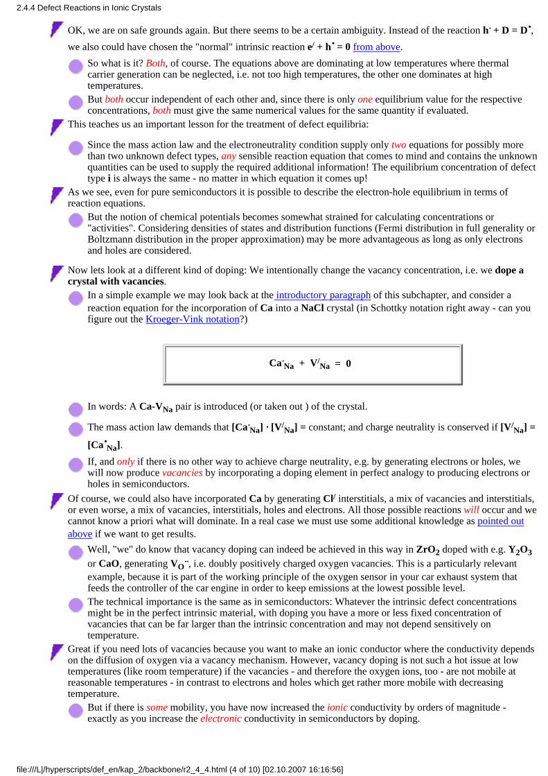
OK, we are on safe grounds again. But there seems to be a certain ambiguity. Instead of the reaction h· + D = D·,we also could have chosen the "normal" intrinsic reaction e/ + h· = 0 from above.
So what is it? Both, of course. The equations above are dominating at low temperatures where thermalcarrier generation can be neglected, i.e. not too high temperatures, the other one dominates at hightemperatures.But both occur independent of each other and, since there is only one equilibrium value for the respectiveconcentrations, both must give the same numerical values for the same quantity if evaluated.
This teaches us an important lesson for the treatment of defect equilibria:
Since the mass action law and the electroneutrality condition supply only two equations for possibly morethan two unknown defect types, any sensible reaction equation that comes to mind and contains the unknownquantities can be used to supply the required additional information! The equilibrium concentration of defecttype i is always the same - no matter in which equation it comes up!
As we see, even for pure semiconductors it is possible to describe the electron-hole equilibrium in terms ofreaction equations.
But the notion of chemical potentials becomes somewhat strained for calculating concentrations or"activities". Considering densities of states and distribution functions (Fermi distribution in full generality orBoltzmann distribution in the proper approximation) may be more advantageous as long as only electronsand holes are considered.
Now lets look at a different kind of doping: We intentionally change the vacancy concentration, i.e. we dope acrystal with vacancies.
In a simple example we may look back at the introductory paragraph of this subchapter, and consider areaction equation for the incorporation of Ca into a NaCl crystal (in Schottky notation right away - can youfigure out the Kroeger-Vink notation?)
Ca·Na + V/
Na = 0
In words: A Ca-VNa pair is introduced (or taken out ) of the crystal.
The mass action law demands that [Ca·Na] · [V/
Na] = constant; and charge neutrality is conserved if [V/Na] =
[Ca·Na].
If, and only if there is no other way to achieve charge neutrality, e.g. by generating electrons or holes, wewill now produce vacancies by incorporating a doping element in perfect analogy to producing electrons orholes in semiconductors.
Of course, we could also have incorporated Ca by generating Cl/ interstitials, a mix of vacancies and interstitials,or even worse, a mix of vacancies, interstitials, holes and electrons. All those possible reactions will occur and wecannot know a priori what will dominate. In a real case we must use some additional knowledge as pointed outabove if we want to get results.
Well, "we" do know that vacancy doping can indeed be achieved in this way in ZrO2 doped with e.g. Y2O3or CaO, generating VO
··, i.e. doubly positively charged oxygen vacancies. This is a particularly relevantexample, because it is part of the working principle of the oxygen sensor in your car exhaust system thatfeeds the controller of the car engine in order to keep emissions at the lowest possible level.The technical importance is the same as in semiconductors: Whatever the intrinsic defect concentrationsmight be in the perfect intrinsic material, with doping you have a more or less fixed concentration ofvacancies that can be far larger than the intrinsic concentration and may not depend sensitively ontemperature.
Great if you need lots of vacancies because you want to make an ionic conductor where the conductivity dependson the diffusion of oxygen via a vacancy mechanism. However, vacancy doping is not such a hot issue at lowtemperatures (like room temperature) if the vacancies - and therefore the oxygen ions, too - are not mobile atreasonable temperatures - in contrast to electrons and holes which get rather more mobile with decreasingtemperature.
But if there is some mobility, you have now increased the ionic conductivity by orders of magnitude -exactly as you increase the electronic conductivity in semiconductors by doping.
2.4.4 Defect Reactions in Ionic Crystals
file:///L|/hyperscripts/def_en/kap_2/backbone/r2_4_4.html (4 of 10) [02.10.2007 16:16:56]

Moreover, you know the concentration of the vacancies, and within some parameter range, you can treat it asconstant which means you can remove [V] from the business end of the mass action law and multiply it intothe general reaction constant. Life is easier.
There are more examples for technical uses of doping, but we will now consider the third basic reactions, thedefect reactions at interfaces.
Defect Reactions at Interfaces
Considering that all chemical reactions between a solid and anything else occur at the surface of the solid, i.e. atthe solid-gas, solid-liquid, or solid- solid interface, this headline covers a good part of general chemistry.
Indeed, it has become clear in recent years that reactive solid-solid interfaces generate or consume pointdefects. However, here we will only look at reactions between a gas and a (simple) ionic crystal as they areused in sensor technology. In other words, we consider the possible reactions between a MeX crystal and aX2(g) gas in a first simplified treatment. We do not consider charges for the time being, to keep thingssimple.The crystal may then incorporate X2(g) (or emit it) via several reactions which we can easily formulate withthe the Kröger-Vink notation:
1. ½X2(g) + Vx = Xx
i.e. an atom of the gas occupies a fitting empty place (= vacancy) of the crystal.
2. ½X2(g) + Vi = Xi
i.e. an atom of the gas occupies a fitting empty place (= vacancy) in the interstitial lattice and is now aninterstitial.
3. ½X2(g) + VM = XM
i.e. an atom of the gas occupies a (probably not well fitting) empty place (= vacancy) in the metal ion latticeand is now an anti-site defect.
And there will be even more possibilities as is shown below.
The thing to note once more is: If these reactions can occur, they will occur - independently of each other. Onlytheir probabilities (or reaction rates) are (wildly) different, and we are well off if we know (or can make aneducated guess) at the dominating reaction. And the equilibrium concentrations [Di] of some defect type Di, nomatter in which equation it appears, are always identical in equilibrium.
In other words, we should know
What kind of defect situation dominates in our MeX crystal (Frenkel- or Schottky defects etc.); i.e.which reaction constant is smallest?
1.
How can charge neutrality be achieved (only with ions and defects; only with electrons and holes, orin a mixture)? In other words are we dealing with an ionic conductor, a semiconductor, or a mixedcase? Of course, the answer to this question may well depend on the temperature.
2.
Is there intentional (or unintentional) ionic or electronic doping that imposes specific conditions onthe defect situation?
3.
This only looks hopeless, but rejoice, it is not - albeit for a sad reason: After all, we are not so much interested indefects per se, but in their uses. Typically, we want to do something "electrical" - make a better battery, a fuelcell, a sensor giving of a voltage or a current in response to the stuff to be sensed - and this demands that we useonly ionic crystals that are ionic conductors of some sort.
2.4.4 Defect Reactions in Ionic Crystals
file:///L|/hyperscripts/def_en/kap_2/backbone/r2_4_4.html (5 of 10) [02.10.2007 16:16:56]

Unfortunately, not too many ionic crystal are useful ionic conductors; it's just a handful of crystal families.And only those families we have to know. The search for a real good (and affordable) ionic conductor atroom temperature is still on - if you find it, you may not make the Nobel prize, but certainly a great deal ofmoney.So all it takes is to study some 4 or 5 typical cases which contain practically everything encountered in ionicdefect engineering.
The paradigmatic case is an undoped crystal with Frenkel defects and some semiconducting properties. We startassuming that the electron/hole concentration is far smaller than the Frenkel defect concentration.
Thermal equilibrium of the MeX crystal by itself thus means that we have
[M·i] = [V/
M]
[e'] = [h·] << [VM]
Now we establish equilibrium with the gas X2(g). It could be H2, O2, Cl2, F2, whatever.
How are X atoms to be incorporated? Surprisingly, perhaps, none of the three possibilities given above is thepreferred reaction. We do not have X- vacancies (Vx) available in our case, and we are not going to generatevery unlikely X interstitials (Xi') or anti site defects. We want to incorporate X on a regular lattice site.
Now you see why the Kröger-Vink notation is useful. Playing around a bit with what you have (and puttingin charge neutrality right away), gives
½ X2(g) + MM = MX + V/M + h·
In words: An X-atom takes out a M atom from its position on the crystal surface, forming a MX moleculethat is added to the crystal somewhere, leaving back a vacancy on a M-site and a hole.This is not so easily expressible in Schottky notation (try it), but leads easily to the mass action law noticingthat [MM] = [MX] = const = 1 and thus not needed in the "business end" of the mass action law.
We could come up with other reaction equations achieving the same result; but the one we have is goodenough for the time being.
We thus obtain two "master" equations for this case, one from mass action and one from charge neutrality exactlyalong the lines discussed before.
Mass action law
[X2(g)]1/2
[V/M] · [h·]
= const.
Charge neutrality
[V/M] + [e/] = [Mi
·] + [h·]
2.4.4 Defect Reactions in Ionic Crystals
file:///L|/hyperscripts/def_en/kap_2/backbone/r2_4_4.html (6 of 10) [02.10.2007 16:16:56]

We have two equations for the four unknowns V/, e/, Mi·, and h· which determine the electrical conductivity
σ as a function of the concentration (or partial pressure) of the gas [X2(g)] via
σ([X2(g)]) = Σi (qi · ci · µi)
With q = charge carried by the defect i, ci = concentration and µi = mobility of defect i, resp.
Again, we need to have additional information about our system if we want quantitative relations between ameasurable parameter like the defect-dependent conductivity.
Doping, as described above, could be helpful. It would provide a more or less constant value for e.g. thevacancy or electron concentration and thus remove one (or two) unknowns.Without that, however, we have to resort to case studies making reasonable assumptions and considering theimportant quantities for the task at hand. As an example, if we want to measure the [X2(g)] concentration,we are not so much interested in the absolute value of σ, but in its change with the gas concentration,dσ/d[X2(g)].
That implies that we are mainly interested in those defects which react sensitively to concentration changesof [X2(g)].
For our example we postulated the two conditions
[M·i] = [V/
M]
[e/] = [h·] << [VM/]
This is valid as long as we are considering stoichiometric MX which is neither losing nor adding X. In otherwords, the crystal is kept at the stoichiometric point - at a certain partial pressure of X2.
It is now important to notice that the reaction with the outside gas at partial pressures different from thatbelonging to the stoichiometric point changes the stoichiometry - no matter how you look at it. For ambient(or standard) pressure, there is no reaction and the stoichiometry is perfect - we are at the stoichiometricpoint. For large partial pressures of X2, we will produce MX1 +δ, , for low pressures MX1 – δ, .
Now lets see what happens if we work around the stoichiometric point. The absolute concentration of thevacancies and interstitials may change a little, and this means that the electron and hole concentration has tochange exactly the same amount in order to maintain charge neutrality.
However, since we assumed that the absolute concentration of the electrons and holes at the stoichiometricpoint is much smaller than that of the vacancies and interstitials, the relative change of [e/] and [h·] is muchlarger than that of [Mi
·] and [V/M].
Accordingly, we may assume that [Mi·] and [V/
M] ≈ constant around the stoichiometric point, i.e. within acertain range of partial pressures of X2 below and above the standards pressures which simplifies therelevant equations to
[X2(g)]1/2
[h·] = const.
With a different value of the constant, however.
2.4.4 Defect Reactions in Ionic Crystals
file:///L|/hyperscripts/def_en/kap_2/backbone/r2_4_4.html (7 of 10) [02.10.2007 16:16:56]

The concentration of holes and electrons, on the other hand, changes markedly, but their absoluteconcentrations are still much smaller than that of vacancies and interstitials.
This leads us to an extremely important generalization:
As far as the mass action law is concerned, only variable concentrations, i.e. concentrations that are not(approximately) constant, count. The absolute concentration is of no special importance - it becomes part ofthe reaction constant.As far as charge neutrality is concerned, only absolute concentrations count. Minority carriers can simply beneglected in a first approximation.
This give a first direct result: We can write dow the following simplified mass action law and electroneutralitycondition:
Massaction [h·] = const · [X2(g)]1/2
Electro-neutrality
[V/M] = [Mi
·]
How about the electron concentration? Since our approximations imply that there is no interaction between the
point defects and the electrons and holes, we must have [h·] · [e'] = const. and thus
[e/] = const · [X2(g)]–1/2
But we will derive that result now by using different reaction equation just to show that in equilibrium youalways must obtain the same results.
Lets consider the reaction
½ X2(g) + M·i + e/ = MX + Vi
In words: A positively charged metal interstitial plus an electron and a gas atom form a crystal molecule anda vacancy on the interstitial lattice.
Neglecting M·i, MX, and Vi with the same arguments as before, we have, as we know that it must be
[e/] = const · [X2(g)]–1/2
In a log [i] - log [X2(g)] plot we have straight lines with a slope of 1/2 for holes, – 1/2 for electrons and 0 for theinterstitials and vacancies, respectively. This looks like this:
2.4.4 Defect Reactions in Ionic Crystals
file:///L|/hyperscripts/def_en/kap_2/backbone/r2_4_4.html (8 of 10) [02.10.2007 16:16:56]

Without looking at the reaction constants, we know that the cross over of the e/ and h· concentration linesmust be at the stoichiometric point.It is clear that for large deviations from the stoichiometric point the approximations used are no longer valid.For very small or very large partial pressures of X2, we now may consider the other two possible extremesby simply extrapolating the lines in the illustration:
1. For very large partial pressures of X2 the e/ concentration becomes negligible while the hole concentrationbecomes comparable to the point defect concentration. Charge neutrality can only be maintained bydecreasing the positively charged metal interstitials and increasing the negatively charged vacancies. In theextreme, we may only consider [V/
M] = [h·] for charge neutrality. Inserting that in the reaction equation fromabove, we have .
½ X2(g) + MM = MX + 2h·
which gives the mass action equation
[X]1/2
[h·]2 = const
[h·] = const. · [X]1/4
For very low partial pressures we obtain exactly along the same line of arguments [e/] = const. · [X]–1/4.
With these relations, we may also calculate the concentrations of the minority point defects by simply insertingthe above equations in the appropriate reaction equation and applying mass action which yields
High pressureside
[Mi·] = const · [X]–1/4
Low pressure
side[V/
M] = const · [X]1/4
Putting everything together in on single graph, we obtain a schematic Kröger-Vink or Brouwer diagram:
2.4.4 Defect Reactions in Ionic Crystals
file:///L|/hyperscripts/def_en/kap_2/backbone/r2_4_4.html (9 of 10) [02.10.2007 16:16:56]

Of course, the change-over would be smooth in reality; and we cannot tell easily where it will occur. It isalso obvious that there are no discontinuities of the concentration curves, which tells us something about the"const." in the mass action equation.In the consideration above we did not assign values to the "const." and carry it through. That might be ainteresting exercise one of those days.
In any case, we now have seen how Kröger-Vink reaction equations, mass action, charge neutrality and someadditional knowledge or educated guesses allow to come up with a pretty good idea of what will happen in areaction involving point defects.
The possibilities of electronic and ionic doping together with the temperature dependence of point defectequilibria now give us a powerful tool for designing materials for specific applications."Ionics", in research and application, is slowly coming into its own. Together with the good old "electronics"it may well open up new fields for materials scientists.
2.4.4 Defect Reactions in Ionic Crystals
file:///L|/hyperscripts/def_en/kap_2/backbone/r2_4_4.html (10 of 10) [02.10.2007 16:16:56]

3. Point Defects and Diffusion
3.1 General Remarks
3.1.1 Diffusion and Point Defects
3.1.2 Recapitulation of Ficks Laws
3.1.3 Coupling Phenomenological Laws to Single Atomic Jumps
3.2 Diffusion Mechanism
3.2.1 Atomic Mechanisms
3.2.2 Self-Diffusion
3.2.3 Diffusion of Impurity Atoms
3.3 Experimental Approaches to DiffusionPhenomena
3.3.1 Determination of Diffusion Profiles
Contents of Chapter 3
file:///L|/hyperscripts/def_en/kap_3/backbone/r3.html [02.10.2007 16:16:57]
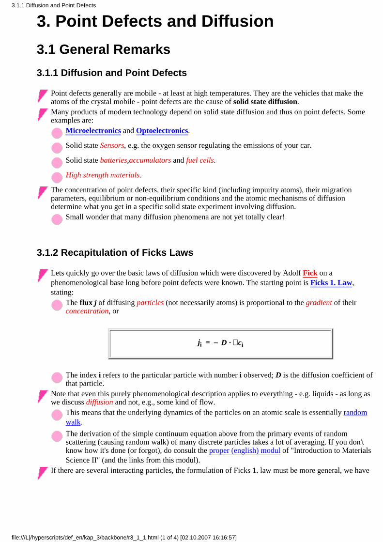
3. Point Defects and Diffusion
3.1 General Remarks
3.1.1 Diffusion and Point Defects
Point defects generally are mobile - at least at high temperatures. They are the vehicles that make theatoms of the crystal mobile - point defects are the cause of solid state diffusion.Many products of modern technology depend on solid state diffusion and thus on point defects. Someexamples are:
Microelectronics and Optoelectronics.
Solid state Sensors, e.g. the oxygen sensor regulating the emissions of your car.
Solid state batteries,accumulators and fuel cells.
High strength materials.
The concentration of point defects, their specific kind (including impurity atoms), their migrationparameters, equilibrium or non-equilibrium conditions and the atomic mechanisms of diffusiondetermine what you get in a specific solid state experiment involving diffusion.
Small wonder that many diffusion phenomena are not yet totally clear!
3.1.2 Recapitulation of Ficks Laws
Lets quickly go over the basic laws of diffusion which were discovered by Adolf Fick on aphenomenological base long before point defects were known. The starting point is Ficks 1. Law,stating:
The flux j of diffusing particles (not necessarily atoms) is proportional to the gradient of theirconcentration, or
ji = – D · ∇ci
The index i refers to the particular particle with number i observed; D is the diffusion coefficient ofthat particle.
Note that even this purely phenomenological description applies to everything - e.g. liquids - as long aswe discuss diffusion and not, e.g., some kind of flow.
This means that the underlying dynamics of the particles on an atomic scale is essentially randomwalk.
The derivation of the simple continuum equation above from the primary events of randomscattering (causing random walk) of many discrete particles takes a lot of averaging. If you don'tknow how it's done (or forgot), do consult the proper (english) modul of "Introduction to MaterialsScience II" (and the links from this modul).
If there are several interacting particles, the formulation of Ficks 1. law must be more general, we have
3.1.1 Diffusion and Point Defects
file:///L|/hyperscripts/def_en/kap_3/backbone/r3_1_1.html (1 of 4) [02.10.2007 16:16:57]

ji = – M · ∇µi
With µ = chem. potential; M = mechanical mobility.
Since the gradient of the chemical potential may be different from zero even for constantconcentrations, special effects as, e.g., uphill diffusion are contained within this formulation.
The next basic equation is the continuity equation. It states:
Changes of the particle concentration within a volume element must express the difference of whatgoes in to what goes out - we have conservation of the particle number here. In mathematical termsthis means
∂c
∂t = – div j
This is if course only true as long as no particles are generated or annihilated (as, e.g., in the case ofelectrons or holes in an illuminated semiconductor).
Combining the two equations from above we obtain Ficks 2. law:
The temporal change in concentration at a given point is proportional to the 2nd derivative of theconcentration, or
∂c
∂t = div (D · ∇c) = D · ∆c
With the final equation being valid only for D = const.
Ficks equations look innocent enough, but solutions of the rather simple differential equations formingFicks laws are, in general not all that simple! They do follow some general rules, however:
They involve almost always statistical functions, as well they should, considering that diffusion is atotally statistical process at the atomic level.The solutions to heat conducting problems are quite similar, as well they should, because theconduction of heat can be treated as a diffusion phenomena. (it actually is a diffusion phenomena).This link gives some more information about Fick's laws and standard solutions.
Many diffusion phenomena can be dealt with on the phenomenological base of Ficks laws. All that isrequired, is to know the diffusion coefficient and its dependence on temperature and possibly othervariables - you do not have to know anything about the atomic mechanisms involving point defects tosolve diffusion problems.
It turns out, however, that complex diffusion problems - e.g. the simultaneous diffusion of B and Pin Si can not be modeled adequately without knowing the atomic mechanisms and their interaction.This explains the impetus behind major efforts to unravel the precise mechanisms of diffusion in Siand other semiconductors.
3.1.1 Diffusion and Point Defects
file:///L|/hyperscripts/def_en/kap_3/backbone/r3_1_1.html (2 of 4) [02.10.2007 16:16:57]

3.1.3 Coupling Phenomenological Laws to Single Atomic Jumps
We now must link the phenomenological description of diffusion (that only works on averages and thusonly if many particles are considered) with the basic diffusion event, the single jump of a single atom ordefect.We describe the net flux of particles as the difference in the number of particle jumps to the left and tothe right. With the jump frequency ν we obtain Ficks 1. law with an expression for the diffusioncoefficient (for cubic crystals), a detailed derivation is given in the link.
D = g · a2 · ν
With a = lattice constant, ν = jump frequency, i.e. the number of jumps from one position to aneighboring one per sec.g is the geometry factor of the lattice type considered. It takes into account that considering alljumps that are possible in the given lattice, only some have a component in the x-direction. Itsdefinition is
g = ½ · Σi ∆xi
a
g is always about 1 as you will find out doing the exercise, so we will not consider it any more.
The jump frequency ν is given by
ν = ν0 · exp –Gm
kT
with Gm = free enthalpy for the jump or for the migration of the atom or defect.
This gives us the second important parameter set describing a property of a point defect, namely itsmigration energy and entropy
All we have to do is to express Gm = HM – TSM, with HM = migration enthalpy (or -energy), andSM = migration entropy.
The magnitude of the migration entropy will be comparable to the formation entropy because it hasthe same roots. It is thus around 1 k for "normal" crystals.
Combining everything, we obtain an expression for the diffusion coefficient D in terms of the migrationenergy:
D = D0 · exp –HM
kT
3.1.1 Diffusion and Point Defects
file:///L|/hyperscripts/def_en/kap_3/backbone/r3_1_1.html (3 of 4) [02.10.2007 16:16:57]

Where all constant (or nearly constant) factors have been included in D0. Some numerical valuesare given in the link.
These formulas relate the atomic properties of defects to the diffusion coefficient from Ficks laws.
There is one more expression of prime importance when it comes to diffusion. It brings togetherstatistical considerations from looking at random walk (which is what a vacancy does). It is, of course,the famous Einstein - Smoluchowski relation (for 3-dimensional diffusion).
D = L2
6τ
With L = mean square displacement or diffusion length, τ = time since start of the diffusion (or, ifthe particle "dies", e.g. by recombination in the case of minority carriers in semiconductors, itslifetime).
Einstein derived this in 1905 in a slightly more general form:
D = <r 2>
g* · τ
With r = vector between "start" and "stop" of the diffusing particle for the time τ; <r2> is thus theaverage of the square of the mean displacement (this is something different from the square of theaverage!), and g* is some factor "in the order of 1", i.e. 2, or 6, depending if the diffusion is 1 -, 2 -or 3 -dimensional and what kind of symmetry (cubic, etc.) is involved.
Now let's do an exercise:
Exercise 3.1-1
Calculate geometry factors
3.1.1 Diffusion and Point Defects
file:///L|/hyperscripts/def_en/kap_3/backbone/r3_1_1.html (4 of 4) [02.10.2007 16:16:57]

3.2 Diffusion Mechanism
3.2.1 Atomic Mechanisms
There are several atomic mechanisms that lead to the movement of atoms. By far the most prominent are the vacancymechanism and the direct interstitial mechanism. How they work can be seen in the animations:
Simulation of the vacancy mechanism Simulation of the directinterstitial mechanism
Note a fundamental difference! If you consider the diffusion of a particular atom (any blue one of your choicefor the vacancy mechanism, any one of the red ones for the interstitial mechanism), your selected atom alwaysmoved a bit in the second case, but may not have done anything in the first case. The diffusion of a particularlattice atom by a vacancy mechanism, while inextricably linked to the movements of vacancies, is not the sameas vacancy diffusion, but something different!In other words: if a vacancy has made N jumps by moving around in the lattice, N atoms will also have made ajump. However, not necessarily N different atoms, because some individual atoms may have made more than 1jump. If we look at any particular atom, there is no way of telling if ti has made a jump or not. At best we cangive some probability.This leads to a major conclusion: While the diffusion of a particular lattice atom by a vacancy mechanism isinextricably linked to the movements of many vacancies, its specific movement is principally different from themovement of a single vacancy.
Other mechanisms which are quite rare but nonetheless potentially important in semiconductors are:
Indirect interstitial mechanismfor self-interstitials
The simulation shows theelementary step: Aself-interstitial (shown inlight blue for easieridentification) pushes a latticeatom into the interstitiallattice. The net effect is themigration of anself-interstitial from oneinterstitial site to an differentone.
3.2.1 Atomic Mechanisms
file:///L|/hyperscripts/def_en/kap_3/backbone/r3_2_1.html (1 of 3) [02.10.2007 16:16:57]

The mechanism is totallydifferent from the regularinterstitial mechanism. If in athought experiment you marka specific self-interstitial atom(paint it red), it will move alot with the direct interstitialmechanism, but hardly at allwith the indirect one.
The "kick-out" mechanismfor impurity atoms
Interstitial impurity atomsmove rather fast by a directinterstitial mechanism, untilthey eventually displace alattice atom. This is shown inthe simulation. We now havea self-interstitial (that may ormay not be very mobile) anda rather immobilesubstitutional impurity atom,which may now diffuse withone of the other (slow)mechanisms.The total effect of thediffusion now is caused bythe superpositon of two(usually very different)mechanisms. Au in Si, andpossibly some otherimpurities, diffuse in thisfashion.
The Frank-Turnbull mechanisms(or dissociative mechanism).
This is the pendant to thekick-out mechanism. Here thediffusing impurity atom doesnot dislodge a lattice atom,but gets trapped in a vacancy,whereupon it is almostimmobile. The total effectmay be quite similar to thekick-out mechanism.Which mechanism -Frank-Turnbull or kick-out -is operative, is difficult tofind out. We must expect thatin materials containingpredominantly vacancies, theFrank-Turnbull mechanismwill occur for someimpurities, while the kick-outmechanism may be operativein materials with sizeableconcentrations of interstitials.
3.2.1 Atomic Mechanisms
file:///L|/hyperscripts/def_en/kap_3/backbone/r3_2_1.html (2 of 3) [02.10.2007 16:16:57]

Various direct diffusion mechanismsShown is one variant, a directexchange of places betweentwo atoms. Other variants areexchanges involving morethat 2 atoms (a whole "ring"that "rotates").Direct mechanisms are everynow and then suggested in theliterature to account for somenew diffusion phenomena,but so far do not seem tooccur in crystals.They may, however, play arole (in analogous form)when considering diffusion inamorphous materials.
Then we could have:
The "Extended interstitial" mechanismThis is a possibility not yet discussed or observed. It is mentioned just to show that there might be more atomicmechanisms than have been discovered so far. Imagine an extended interstitial moving through a crystal. The 10or so atoms "inside" the extended interstitial move around a bit while the interstitial passes through and may endup on lattice places different from the ones where they were - they have moved! It is totally unknown if thiseffect plays a role in Si, but it well might occur at high temperatures.And, maybe, there could be more?
Again, it is important to keep in mind that you must clearly keep apart the movement of the "vehicle" - the vacancy,interstitial, etc. - and the movement of the atom(s) whose diffusion is of interest to you!
3.2.1 Atomic Mechanisms
file:///L|/hyperscripts/def_en/kap_3/backbone/r3_2_1.html (3 of 3) [02.10.2007 16:16:57]

3.2.2 Self-Diffusion
We ask ourselves how the regular atoms of a crystal diffuse. In the case of crystals with two or more differentatoms, we have to answer this question for each kind of atom separately. The answer is easiest for a simple (mono)vacancy mechanism in simple elemental cubic crystals. Theself-diffusion coefficient is given by g · a2 times the number of jumps per sec that the diffusing particles make.
Since only lattice atoms that have a vacancy as a neighbor can jump, or, in other words, the number of latticeatoms jumping per sec is identical to the number of vacancies jumping per sec, we obtain for the diffusioncoefficient of self-diffusion by a simple vacancy mechanism the following equations:
DSD = cV · Dv
DSD = g · a2 · n 0 · exp –Gm
kT · exp –
GF
kT
DSD = g · a2 · ν 0 · exp SM
k · exp –
Hm
kT · exp
SF
k · exp –
HF
kT
DSD := D* · exp – Hm + HF
kT
Gm is the free enthalpy for a jump, i.e. the free enthalpy barrier that must be overcome between two identicalpositions in the lattice.In words: All the material dependent constants (including the migration and formation entropy) have beenlumped together in D*; and the exponential now contains the sum of the migration and formation energy of avacancy.
Lets discuss this equation a bit:
As mentioned before, we need an entropy of migration as a parameter of a point defect. In summary we needfour parameters correlated with an intrinsic point defect to describe its diffusion behavior (if we discount thevibration frequency).But only two parameters, the formation energy and the migration energy are of overwhelming importance.
Everything else may be summarized in a (more or less) constant pre-exponential factor D* which containsthe entropies. Since the entropies may be temperature dependent (for Si this is probably the case), you mustlook at bit closer at your calculations if you are interested in precise diffusion data.An Arrhenius-representation (lg D vs. 1/T) will give a straight line, the slope is given by HM + HF. Thepre-exponential factor determines the intersection with the axis and is thus measurable.Since it is much easier to measure diffusion coefficients compared to point defect densities, the sum HM +HF for point defects is mostly much better known than the individual energies. Some values are given in thelink.Self-diffusion vial self-interstitials follows essentially the same laws.
For self-diffusion in Si, we find the following (rather small) values : DSD = (10–21 — 10–16) m2/s in the relevanttemperature regime. Detailed data in an Arrhenius plot for for self-diffusion in Si can be found in the link; somenumbers for Si self-diffusion as well as the migration parameters of vacancies and interstitials and a few elementsare also illustrated.
Now for an exercise. Self-diffusion means that the atoms in a crystal change their position. After some time allatoms will have changed their positions at least once.
3.2.2 Self-Diffusion
file:///L|/hyperscripts/def_en/kap_3/backbone/r3_2_2.html (1 of 2) [02.10.2007 16:16:57]

Our crystal just lying there, somehow changes identity. What does it mean? How long does it take? Do theexercise 3.2-1!
Exercise 3.2-1
Crystal Identity
3.2.2 Self-Diffusion
file:///L|/hyperscripts/def_en/kap_3/backbone/r3_2_2.html (2 of 2) [02.10.2007 16:16:57]

—
3.2.3 Diffusion of Impurity Atoms
Diffusion of Impurity Atoms via Vacancies or Self-Interstitials
In this case it is especially important not to confuse the vehicle (a point defect except in the case of the directinterstitial diffusion) with the diffusing impurity atom.
What we want to have are the diffusion data for the impurity atom, not for the vehicle! We will not go intodetails at this point, but it will come up later again.
Direct diffusion
This is the simplest mechanism, it does not need point defects. It only works for interstitial impurity atoms. Thediffusion coefficient Ddir is simply given by
Ddir = g · a2 · ν 0 · exp S
k · exp –
Hm
kT
With Hm, Sm being the enthalpy and entropy of the jumping impurity atom.
This is in most cases a sufficiently good approximation. The host lattice only enters in the form of the latticefactor g (and to some extent in the migration entropy), but plays no other role. This is of course a source ofpossible aberrations, because the ideal lattice implied in this case does normally not exist. Good examples fordirectly diffusing impurities are O in Si, but there are many other elements.
The following table (taken from K. Graff, Metal Impurities in Si-Device Fabrication; Springer Series inMat. Science 24) gives a few more examples.
Interstitial Impurity Atom Diffusion in Si
Metal HSol [eV] SSol [k] Hm [eV] D*[m2/s] T-regime [0C]
Ti 3,05 4,22 1,79 1,45x10⁻² 950 - 1200
Cr 2,79 4,7 0,99 1,0x10⁻² 900 - 1250
Mn 2,80 7,11 0,6 5,7x10⁻⁴ 900 - 1200
Fe 2,94 8,2 0,68 1,3x10⁻³ 30 - 1200
Co 2,83 7,6 0,53 4,2x10⁻³ 900 - 1100
Ni 1,68 3,2 0,47 2,0x10⁻³ 800 - 1300
Cu 1,49 2,4 0,43 4,7x10⁻³ 400 - 900
HSol and SSol denote the solubility enthalpies and -entropies. This is the extrinsic point defect quivalent ofthe formation enthalpy and entropy of intrinsic point defects.
3.2.3 Diffusion of Impurity Atoms
file:///L|/hyperscripts/def_en/kap_3/backbone/r3_2_3.html (1 of 2) [02.10.2007 16:16:57]

Here are some links illustrating impurity diffusion:
From a review of U. Gösele, we take the Arrhenius plot for many impurity atoms in Si.
In this link we have a somewhat unusual way of showing impurity diffusion in Si.
Here some specialities: Frank-Turnbull and Kick-out Mechanism in Si
U. Gösele essentially "invented" the kick-out mechanism around 1985 and demonstrated that it not onlyprovided an alternative to the already known Frank-Turnbull Mechanism, but does most likely control thediffusion of Au, Pt, and possibly Zn in Si.The two mechanisms, although similar in many ways, lead under certain circumstances to very differentdiffusion profiles, as shown in the graph below taken from a review article (Fast Diffusion inSemiconductors) accessible through the link.
Often it is quite difficult to decide from the data what kind of mechanism is operative. During the last fewyears, some research groups studying diffusion in GaAs came to the conclusion that the diffusionmechanisms in GaAs might be very different from what was accepted before (invoking, e.g., a kick-outmechanism).There is no evidence so far that impurity diffusion in crystals of any kind of crystal involves a directmechanism. Direct mechanisms, however, are periodically suggested in the literature and should not beruled out per se.
So, what is the Message of this sub-chapter?
Many diffusion phenomena, especially in semiconductors or more complicated crystals, are still not verywell understood. Precise modeling of diffusion, however, depends sooner or later on using the correctmechanisms.Data from diffusion measurements are always (sometimes "encrypted") data on point defects.
3.2.3 Diffusion of Impurity Atoms
file:///L|/hyperscripts/def_en/kap_3/backbone/r3_2_3.html (2 of 2) [02.10.2007 16:16:57]

3.3 Experimental Approaches to Diffusion Phenomena
3.3.1 Determination of Diffusion Profiles
General Remarks
In a typical diffusion experiment, some impurity atoms are introduced into a host by first putting them (ideally) with δ -distribution at the surface.
After annealing for a specified time at a specified temperatures, some diffusion of the impurity atoms will have produced adiffusion profile, i.e. a smooth curve of the concentration c vs. depth x in the sample (usually plotted as lg(c) - x curve).Some experimental care is necessary. Simply depositing the impurity atoms on the surface of the host crystal may not leadto any results, because e.g. an impenetrable oxide layer may prevent any diffusion of the impurity atoms into the crystal."Shooting" the impurity atoms into a surface-near area via ion implantation will overcome that problem, but may create itsown problems by generating point defects which change the regular diffusion behavior.There are some well established standard methods for measuring the diffusion profiles after a successful diffusionexperiment (see below). Fitting the profile to the applicable solution of Ficks law will provide two results:
The numerical value of the diffusion coefficient D for the set of parameters considered.1.
The validity of Ficks law for this case as evidenced by the quality of the fit.2. Of course, any "macroscopic" method for measuring profiles relies on having a profile on a, lets say, 10 µm scale in thefirst place, i.e. each impurity atom must have made many individual jumps.This will in most cases only happen at sufficiently high temperatures. Waiting a long time is not very effective; this isimmediately clear if looking at diffusion phenomena in a slightly different way.
How then do we get experimental data at small concentrations or small numbers of jumps? The answer is: use radioactive traceratoms as the diffusing atoms, that can be found and identified in extreme small concentrations!
Tracer Techniques
Radioactive tracer atoms can be easily detected whenever they decay, emitting some high energy radiation.
If the half-life time of the tracer used is relatively small (but still large enough to allow an experiment before the tracer hasvanished), a large percentage of the tracer atoms can be detected by their decay products - typically α, β, or γ-rays. We thusmay have an extremely high detection efficiency, many orders of magnitude below the detection limits of standard methods.
Lets consider the general way a tracer experiment is done:
Deposit a thin layer of the atoms that are to diffuse on the (very clean) host crystal. Some of those atoms should be a suitableradioactive isotope of the species investigated. Use any deposition technique that works for you (evaporation, sputteringtechniques, sol-gel techniques ("painting it on")...), but make sure that the deposition technique does not alter your substrate(sputtering, e.g., may produce point defects) and that you have no "barrier layer" between the substrate and the thin layer.Anneal for a suitable time at a specific temperature.
Remove thin layers from the surface (ideally one atomic layer after the other) by, e.g. sputtering techniques, anodic oxidationand chemical stripping, ultramicrotomes, chemical dissolution, ...).Measure the radioactivity of each layer.
With the known half-life of the tracer and the time since the deposition of the layer, calculate how many tracer atoms are inyour layer. From the measurement of many layers a concentration profile of the tracer atoms results.
The rest is conventional: Fit the profile against a standard solution of Ficks law or against your own solution and extract thediffusion coefficient for the one temperature used. This gives one data point. And then:
Repeat the experiment for several other temperatures, collecting data points for different temperatures.
From an Arrhenius representation of the measured diffusion coefficients you obtain D0 and an activation energy for the tracerdiffusion if your data are on a (halfway) straight line.
If this sounds tedious, it's because it is! You appreciate why students doing a master or PhD thesis are so essential to research.Still, nothing beats tracer experiments when it comes to sensitivity and accuracy.
There is, however, a basic problem that we have to discuss if you want to extract information about the vehicle of the tracerdiffusion, i.e. about the vacancies or, in some cases, interstitials from a tracer experiment. This is always the case whendealing with self-diffusion.The diffusion coefficient of the tracer atom is not necessarily identical with the diffusion coefficient for self-diffusion asdefined for the vehicles - usually vacancies.
The reason for this is that the tracer is a specific atom, while we look at many vacancies that help it along - and we must notconfuse the vehicle wih the diffusing impurity (or tracer) atom, as noted before. In particular, the jumps of the tracer atom may becorrelated with the jumps of the individual vacancy coming by.
In other words, whereas a particular vacancy may (and usually does) jump around in a perfect random walk pattern (i.e. eachjump contributes to the mean square displacement of the vacancy), the tracer atom may not move randomly!Lets look at a simple example for a two-dimensional vacancy diffusion mechanism.
3.3.1 Determination of Diffusion Profiles
file:///L|/hyperscripts/def_en/kap_3/backbone/r3_3_1.html (1 of 4) [02.10.2007 16:16:58]

The tracer atom is marked in light blue, it has a vacancy asa neighbor, a jump is possible.
Vacancy and tracer atom have exchanged their positions.
Next, the vacancy will jump again - with equal probability on one of the 6 surrounding atom sites - so it is truly doing arandom walk. And one of those jumps goes back to position 7, with exactly the same probability as to the other availablesites.The "viewpoint" of the tracer atom, however, is different. It will jump back to site 6 with a higher probability than to the sites1 - 5 because a vacancy is available on 6, whereas for the other sites the passing of some other vacancy must be awaited.There is a correlation between jump 1 and jump 2 - there is no random walk. The jumps back will lead to wrong values of themean square displacement, because this combination does not add anything and occurs more frequently as it would for a trulyrandom walk.
The correlation effects between individual jumps of the tracer atom and the random jumps of vacancies can be calculated by arigid theory of diffusion by individual jumps - an outline is given in the advanced section.
As a result, these correlation effects (in all dimensions and for all lattice types) can be dealt with by defining a correlationfactor f that must be introduced into the equations coupling the tracer diffusion to the vacancy diffusion.
We define a correlation coefficient f1V that allows to correlate the diffusion coefficient for the (vacancy driven) self-diffusion,DSD(T), as measured by a tracer experiment, to the diffusion coefficient for self-diffusion, DSd as given by theory via the equation
DSD(T) = f1V · DSd
As an example for a real correlation factor we look at f1V(cub), the correlation factor for self-diffusion mediated by singlevacancies in a cubic lattice. It is given in a good approximation by
f1V(cub) ≈ 1 – 2
z =
5/6 fcc
3/4 bcc
With z = number of nearest neighbors.
To illustrate the correlation phenomena, suppose that f = 0. In this case, even for wildly moving vacancies (DSD >> 0), the traceratoms would not move - we would not observe any diffusion.
This case is fully realized for one-dimensional diffusion, where it is also easy to see what happens - just consider a chain ofatoms with one vacancy:
The vacancy may move back and forth the chain like crazy - the tracer atom (light blue) at most moves between two position,because on the average there will be just as many vacancies coming from the right (tracer jumps to the left) than from the left(tracer jumps to the right).
Correlation coefficients can be calculated - as long as the diffusion mechanism and the lattice structure are known. They are,however, very difficult to measure which is unfortunate, because they contain rather direct information about the mechanism ofthe diffusion. The calculations, however, are not necessarily easy.
3.3.1 Determination of Diffusion Profiles
file:///L|/hyperscripts/def_en/kap_3/backbone/r3_3_1.html (2 of 4) [02.10.2007 16:16:58]

Impurity atoms, which may have some interaction with a vacancy, may show complicated correlation effects because in thiscase the vacancy, too, does no longer diffuse totally randomly, but shows some correlation to whatever the impurity atomdoes.If a kick-out mechanism is active, the tracer atom might quickly be found immobile on a lattice site, whereas another atom -which however will not be detected because it is not radioactive - now diffuses through the lattice. The correlation factor isvery small.
Some examples for correlation coefficients are given in the table for a simple vacancy mechanism (after Seeger). The correctvalue from extended calculations is contrasted to the value from the simple formula given above.
Lattice type coordinationnumber z
f1V ≈ 1 – 2/z f1V (correct)
One dim. lattice
Chain 2 0 0
Two dim. lattices
hex. close packed 6 0.6666 0,56006
square 4 0,5 0,46694
Three dim. lattice
cub. primitive 6 0,6666 0,65311
Diamond 4 0,5 0,5
bcc 8 0,75 0,72722
fcc 12 0,83 0,78146
Other Methods for Measuring Diffusion Coefficients
There is a plethora of methods, some are treated in other lecture courses. In what follows a few important methods are justmentioned.Concentration Profile Measurements
Secondary Ion Mass Spectrometry (SIMS) for direct measurements of atom concentrations. This is the most importantmethod for measuring diffusion profiles of dopants in Si (and other semiconductors).Rutherford Backscattering (RBS) for direct measurements of atom concentrations.
Various methods for measuring the conductivity as a function of depth for semiconductors which corresponds more or lessdirectly to the concentration of doping atoms. In particular:
Capacity as a function of the applied voltage ("C(U)") for MOS and junction structures)●
Spreading resistance measurements●
Microwave absorption.●
Local growth kinetics of defects, e.g. the precipitation of an impurity, contain information about the diffusion, e.g.
Growth of oxidation induced stacking faults in Si●
Impurity -"free" regions around grain boundaries (because the impurities diffused into the grain boundary where theyare trapped).
●
An example for a "diffusion denuded" zone along grain boundaries can be seen in the illustration
Annealing experiments
3.3.1 Determination of Diffusion Profiles
file:///L|/hyperscripts/def_en/kap_3/backbone/r3_3_1.html (3 of 4) [02.10.2007 16:16:58]

These experiments are in a class of their own. In this case point defects which have been rendered immobile in a largesupersaturation, e.g. by rapid cooling from high temperatures, are made mobile again by controlled annealing at specifiedtemperatures. Since they tend to disappear - by precipitation or outdiffusion - measuring a parameter that is sensitive to pointdefects - e.g. the residual resistivity - will give kinetic data.A classical experiment produces supersaturated point defects by irradiation at low temperatures with high-energy electrons (afew MeV). The energy of the electrons must be large enough to displace single atoms - Frenkel pairs may be formed - but notlarge enough to produce extended damage "cascades".Annealing for a defined time at a specified temperature will remove some point defects which is monitored by measuring theresidual resistivity - always at the same very low temperature (usually 4K). Repeating the sequence many times at increasingtemperatures gives an annealing curve. A typical annealing curve may look like this:
What "impurities" means in this context is left open. They may form small complexes, interact with nearby vacancies orinterstitials, or whatever.The interpretation of the steps in the annealing curves as shown above is not uncontested. The "Stuttgart school" around A.Seeger has a completely different interpretation, invoking the "crowdion", than the (more or less) rest of the world.
Methods measuring single atomic jumps
This ultimate tool can be used if the point defects have rather low symmetry. The best example is the dumbbell configurationof the interstitial or interstitial carbon in FeIn the classical experiment the crystal is uniaxially deformed at not too low temperatures. The dumbbells will, given enoughtime, orient themselves in the direction of tensile deformation (there is more space available, so the energy is lower) and thuscarry some of the strain. We have more dumbbells in one of the three possible orientations than in the two other ones (seebelow)
The tensile stress is now suddenly relieved. Besides the purely and instantaneous elastic relaxation, we will now see a slowand temperature dependent additional relaxation because the dumbbells will randomize again. The time constant of thisprocess directly contains the jump frequency for dumbbells. This effect, which exists in many variants, is called "Snoekeffect".
If you do not use a static stress, but a periodic variation with a certain frequency ω, you have a whole new world ofexperimental techniques!
Last, there are methods which monitor the destruction (or generation) of some internal order in the material. The prime techniqueis Nuclear Magnetic Resonance (NMR), which monitors the decay of nuclear magnetic moments which were first oriented in amagnetic field and then disordered by atomic jumps, i.e. diffusion. The Mößbauer effect may be used in this connection, too.
3.3.1 Determination of Diffusion Profiles
file:///L|/hyperscripts/def_en/kap_3/backbone/r3_3_1.html (4 of 4) [02.10.2007 16:16:58]

4. Experimental Techniques for StudyingPoint Defects
4.1 Point Defects in Equilibrium
4.2 Point Defects in Non-Equilibrium
4.3. Specialities
Contents of Chapter 4
file:///L|/hyperscripts/def_en/kap_4/backbone/r4.html [02.10.2007 16:16:58]

4. Experimental Techniques for StudyingPoint Defects
4.1 Point Defects in Equilibrium
Differential Thermal Expansion Method
How can we measure directly the type and concentration of point defects and, if we do it as function oftemperature, extract the formation energies and formation entropies?
Simple question - but there is essentially only one direct method: Measure the change of the lattice constanta, i.e. ∆a, and the change in the specimen dimension, ∆l, (one dimension is sufficient) simultaneously as afunction of temperature.
What you have then is the differential thermal expansion method also called the ∆l/l – ∆a/a method.
This method was invented by Simmons and Balluffi around 1960.
The basic idea is that ∆l/l – ∆a/a (with l = length of the specimen = l(T, defects)) contains the regular thermalexpansion and the dimensional change from point defects, especially vacancies.
This is so because for every vacancy in the crystal an atom must be added at the surface; the total volume ofthe vacancies must be compensated by an approximately equal additional volume and therefore an additional∆l.If we subtract the regular thermal expansion, which is simply given by the change in lattice parameter,whatever is left can only be caused by point defects. The difference then gives directly the vacancyconcentration.For a cubic crystal with negligible relaxation of the atoms into the vacancy (so the total volume of thevacancy provides added volume of the crystal), we have
3
∆l
l –
∆a
a
= cV – ci
With cV = vacancy concentration, ci = interstitial concentration.
We have to take the difference of the concentration because interstitial atoms (coming from a vacancy) donot add volume.
This is quite ingenious and straightforward, but not so easy to measure in practice.
The measurements of both parameters have to be very precise (in the 10– 5 range); you also may have toconsider the double vacancies.But successful measurements have been made for most simple crystals including all important metals, and itis this method that supplied the formation energies and entropies for most important materials.
The link shows a successful measurement of ∆l/l – ∆a/a for Ag + 4% Sb.
Some values mostly obtained with that method are shown in the following table (after Seeger):
4.1.1 Experimental Techniques for Studying Point Defects
file:///L|/hyperscripts/def_en/kap_4/backbone/r4_1_1.html (1 of 4) [02.10.2007 16:16:58]

Element cV at Tm HF [eV] SF [k]
Cu 2 x 10⁻⁴ 1,04 0,3
Ag 1,7 x 10⁻⁴ 0,99 0,5
Au 7,2 x 10⁻⁴ 0,92 0,9
Al 9 x 10⁻⁴ 0,65 0,8
Pb 1,7 x 10⁻⁴ 0,5 0,7
Na 7 x 10⁻⁴
Li 4 x 10⁻⁴
Cd 6,2 x 10⁻⁴
Kr 3 x 10⁻³
Si no values, ∆l/l – ∆a/a = 0 even at ultra-high precision
Positron Annihilation
A somewhat exotic, but still rather direct method is measuring the time constant for positron annihilation as afunction of temperature to obtain information about vacancies in thermal equilibrium.
What you do is to shoot positrons into your sample and measure how long it takes for them to disappear byannihilation with an electron in a burst of γ - rays. The time from entering the sample to the end of thepositron is its (mean) life time τ.
It is rather short (about 10–10 seconds), but long enough to be measured, and it varies with the concentrationof vacancies in the sample. Since electrons are needed for annihilation and a certain overlap of the wavefunctions has to occur, the life time τ is directly related to the average electron concentration available forannihilation.A nice feature of these technique is that the positron is usually generated by some radioactive decay event,and then announces its birth by some specific radiation emitted simultaneously. Its death is also marked byspecific γ rays, so all you have to do is to measure the time between two special bursts of radiation.
Vacancies are areas with low electron densities. Moreover, they are kind of attractive to a positron because theyform a potential well for a positron - once it falls in there, it will be trapped for some time.
Since an average life time of 10–10 s is large enough for the positron, even after it has been thermalized, tocover rather large distances on an atomic scale, some positrons will be trapped inside vacancies and theirpercentage will depend on the vacancy concentration.Inside a vacancy the electron density is smaller than in the lattice, the trapped positrons will enjoy asomewhat longer life span. The average life time of all positrons will thus go up with an increasing numberof vacancies, i.e. with increasing temperature.
This can be easily quantified in a good approximation as follows.
4.1.1 Experimental Techniques for Studying Point Defects
file:///L|/hyperscripts/def_en/kap_4/backbone/r4_1_1.html (2 of 4) [02.10.2007 16:16:58]

Lets assume that on the average we have n0 (thermalized) positrons in the lattice, split into n1 "free"positrons, and n2 positrons trapped in vacancies; i.e.
n0 = n1 + n2
The free positrons will either decay with a fixed rate λ given by λ1 = 1/τ1, (with τ1 = (average) lifetime), orare trapped with a probability ν by vacancies being present in a concentration cV.
The trapped positrons then decays with a rate λ2 which will be somewhat smaller then λ1 because it lives alittle longer; its average lifetime is now τ2.
The change in the partial concentration then becomes
dn1
dt = – (λ1 + ν · cV) · n1
dn2
dt = – λ2 · n2 + ν · cV · n1
This system of coupled differential equation is easily solved (we will do that as an exercise), the startingconditions are
n1(t = 0) = n0
n2(t = 0) = 0
The average lifetime τ, which is the weighted average of the decay paths and what the experiment provides,will be
τ = τ1 ·
1 + τ2 · ν · cV
1 + τ1 · ν · cV
The probability ν for a positron to get trapped by a vacancy can be estimated with relative ease, the followingprincipal "S" - curve is expected. By now, it comes as no surprise that no effect was found for Si.
4.1.1 Experimental Techniques for Studying Point Defects
file:///L|/hyperscripts/def_en/kap_4/backbone/r4_1_1.html (3 of 4) [02.10.2007 16:16:58]

The advantage of positron annihilation experiments is its relatively high sensitivity for low vacancyconcentrations (10–6 - 10–7 is a good value), the obvious disadvantage that a quantitative evaluation of the dataneeds the trapping probability, or cross section for positron capture. Some examples of real measurements and further information are given in the links:Life time of positrons in AgLife time of positrons in Si and Ge.Paper (in German): Untersuchung von Kristalldefekten mit Hilfe der Positronenannihilation
A large table containing values for HF as determined by positron annihilition (and compared to values
obtained otherwise) can be found in the link
Exercise 4.1-1
Derive the Formula for τ
More Direct Methods for Measuring Point Defect Properties
There isn't much. Some occasionally used methods are
Measurements of the resistivity. Very suitable to ionic crystals if the mechanism of conduction is ionictransport via point defects. But you never know for sure if you are measuring intrinsic equilibrium because"doping" by impurities may have occurred.
Specific heat as a function of T. While there should be some dependence on the concentration of pointdefects, it is experimentally very difficult to handle with the required accuracy.Measuring electronic noise. This is a relatively new method which relies on very sophisticated noisemeasurements. It is more suited for measuring diffusion properties, but might be used for equilibriumconditions, too. The illustration in the link shows a noise measurement obtained upon annealing frozen-inpoint defects.
However, the view presented above (and in the chapters before) is not totally unchallenged. There are seriousscientists out there who claim that things are quite different, especially with respect to equilibrium concentrationsof vacancies in refractory metals, because the formation entropy is much higher than assumed.
The method of choice to look at this is calorimetry at high temperature, i.e. the measurement of the specificheat. A champion of this viewpoint is Y. Kraftmakher, who just published a book to this point.
4.1.1 Experimental Techniques for Studying Point Defects
file:///L|/hyperscripts/def_en/kap_4/backbone/r4_1_1.html (4 of 4) [02.10.2007 16:16:58]

4.2 Point Defects in Non-Equilibrium
Quenching Experiments
The basic idea behind these techniques is simple: if you have more point defects than what you wouldhave in thermal equilibrium, it should be easier to detect them. There are several methods, the mostimportant one being quenching from high temperatures. Lets look at this technique in its extreme form:
A wire of the material to be investigated is heated in liquid and superfluid He II (i.e. a liquid with a"∞" large heat conduction) to the desired temperature (by passing current through it).Astonishingly, this is easily possible because the He-vapor produced acts as a very efficient thermalshield and keeps the liquid He from exploding because too much heat is transferred.
After turning off the heating current, the specimen will cool extremely fast to He II temperature (≈1K). There is not much time for the point defects being present at the high temperature in thermalequilibrium to disappear via diffusion; they are to a large percentage "frozen-in". The frozen-inconcentration can now be determined by e.g. measuring the residual resistivity ρres of the wire.
The residual resistivity is simply the resistivity found around 0 K. It is essentially dominated bydefects because scattering of electrons at phonons is negligible.
There are, however, many problems with the quenching technique.
The quenching speed ( ≈ 104 oC/s with the He II technique) may still be too small to definitely ruleout agglomeration off point defects (look at exercise 4.2-1). The cure for this problem is to repeatthe experiments at different quenching speeds and to extrapolate to infinite quenching speed. Whatyou will see may look like the schematic representation below.
Recorded is the residual resistivities after a quenched sample was annealed for some specified timeat the temperature T. This can bedone in-situ; after the anneal the specimen is cooled down againand ρres is measured
Plastic deformation is the next big problem.
The unavoidable large temperature gradients introduced by quenching produce large mechanicalstress which may cause severe plastic deformation or even fracture of the specimen. Plasticdeformation, in turn, may severley distort the concentrations of point defects and fracture of asample simply terminates an experiment.
Finally, impurities, always there, may influence the results.
Since impurities may drastically influence the residual resistance, measurements with "dirty"specimens are always open to doubt. In addition, it is not generally easy to avoid in-diffusion ofimpurity atoms at the high temperatures needed for the experiment.Quenching experiments with Si, for example, did not so far give useful data. If any "good" curveswere obtained, it was invariably shown (later) that the results were due to impurity in-diffusion(usually Fe).
4.2.1 Point Defects in Non-Equilibrium
file:///L|/hyperscripts/def_en/kap_4/backbone/r4_2_1.html (1 of 2) [02.10.2007 16:16:58]

The illustration in the link gives an example for the processes occurring during quenching for Auobtained by calculations and demonstrates the difficulties in extracting data from raw measurements.
Exercise 4.2-1
Diffusion during cooling
Other Methods
If all else fails: try to find agglomerates of point defects looking at your specimen with the transmissionelectron microscope (TEM), with X-ray methods or with any other method that is applicable.
Accept local equilibrium: Don't cool too fast, allow time for agglomerates to form. Conclude fromthe type of agglomerate, from their density and size, and whatever additional information you cangather, what kind of point defect with what concentration was prevalent.This is rather indirect and qualitative, but:
It gives plenty of information. There are many examples where TEM contributed vital information topoint defect research. Especially, it was TEM that gave the first clear indication that self-interstitialsplay a role in thermal equilibrium in Si and some rough numbers for formation energies and migrationenergies (Föll and Kolbesen 1978).
In the link an example of the agglomerates of self-interstitials as detected by TEM is given. The majorexperimental problem in this case was to find the agglomerates. Their density is very low and at therequired magnification huge areas had to be searched.
A very new way of looking at point defects is to use the scanning tunneling microscope (STM) and tolook at the atoms on the surface of the sample. This idea is not new; before the advent of the STM fieldion microscopy was used with the same intention, but experiments were (and are) very difficult to doand severely limited.
One idea is to investigate the surface after fracturing the quenched sample in-situ under ultra-highvacuum (UHV) conditions. This would give the density of vacancies on the fracture plane fromwhich the bulk value could be deduced.An interesting set of STM images of point defects in GaAs from recent research is given in thelink.Vacancies can be seen, but there are many problems: The image changes with time - the density ofpoint defects goes up! Why - who knows?The interpretation of what you see is also difficult. In the example, several kinds of contrastsresulting from vacancies can be seen, probably because they are differently charged or at differentdepth in the sample (STM also "sees" defects one or two layers below the top layer). It needsdetailed work to interprete the images as shown in the link.More recent pictures show the surface of Si or Pt, including point defects, in astonishing clarity.But we still will have to wait a few more years to see what contributions STM will be able to maketowards the understanding of point defects.
4.2.1 Point Defects in Non-Equilibrium
file:///L|/hyperscripts/def_en/kap_4/backbone/r4_2_1.html (2 of 2) [02.10.2007 16:16:58]

4.3. Specialities
Special Methods for Ionic Crystals
In ionic crystals, experimental investigations must follow different routes.
The ∆l/l - ∆a/a method will not work by definition for Frenkel defects, where the concentrations ofvacancies and interstitials are identical and the volume change zero.It might work for Schottky defects and mixed defects. In the latter case, however, it will not bepossible to obtain information for the individual point defect types involved because themeasurement only gives integral numbers.Quenching is difficult if not impossible, because ionic crystals are usually bad heat conductors; thiswill limit the quenching speed to useless values. In addition, ionic crystals tend to be brittle andthey usually fracture upon quenching.Positrons will also be trapped by the negatively charged ions, the technique is not applicable.
And last but not least: it is quite unlikely that what you find are equilibrium numbers anyway,because point defects in ionic crystals are so sensitive to deviations from stochiometry and so on.
Fortunately, there are methods specific for ionic and oxide crystals; most prominent is the measurementof the ionic conductivity which is often mediated by point defects and therefore can be used to gatherinformation about point defects.
Spectroscopic methods (ionic crystal are often transparent) may be applied, too.
Other Methods
Since most properties of crystals are structure sensitive, many more methods exist that give someinformation about point defects. In what follows we give a list of some tools (which might be elaboratedupon in due time):
Deep level transient spectroscopy (DLTS). This is a standard method for the investigation ofimpurity atoms in semiconductors.Electron spin resonance (ESR)
Infra red spectroscopy (IR spectroscopy); especially in the form of Fourier-transformIR-spectroscopy (FTIR). The method of choice to investigate O and C in Si.
4.3.1 Specialities
file:///L|/hyperscripts/def_en/kap_4/backbone/r4_3_1.html [02.10.2007 16:16:58]

5. Dislocations
5.1 Basics
5.1.1 Burgers and Line Vector
5.1.2 Volterra Construction and Consequences
5.2 Elasticity Theory, Energy , and Forces
5.2.1 General Remarks and Basics of Elasticity Theory
5.2.2 Stress Field of a Straight Dislocation
5.2.3 Energy of a Dislocation
5.2.4 Forces on Dislocations
5.2.5 Interactions Between Dislocations
5.3 Movement and Generation of Dislocations
5.3.1 Kinks and Jogs
5.3.2 Generation of Dislocations
5.3.3 Climb of Dislocations
5.4 Partial Dislocations and Stacking Faults
5.4.1 Stacking Faults and Close Packed Lattices
5.4.2 Dislocation Reactions Involving Partial Dislocations
5.4.3 Some Dislocation Details for Specific Lattices
Dislocations and Plastic Deformation
5.5.1 General Remarks
Contents of Chapter 5
file:///L|/hyperscripts/def_en/kap_5/backbone/r5.html [02.10.2007 16:16:58]

5. Dislocations
5.1 Basics
5.1.1 Burgers and Line Vector
The smelting and forging of metals marks the beginning of civilization - the art of working metals was forthousands of years the major "high tech" industry of our ancestors.
Trial and error over this period of time lead to an astonishing degree of perfection, as can be seen allaround us and in many museums. In the state museum of Schleswig-Holstein in Schleswig, you mayadmire the damascene blades of our Viking ancestors.
Two kinds of iron or steel were welded together and forged into a sword in an extremely complicatedway; the process took several weeks of an expert smith's time. All this toil was necessary if you wanteda sword with better properties than those of the ingredients. The damascene technology, shrouded inmystery, was needed because the vikings didn't know a thing about defects in crystals - exactly like theRomans, Greek, Japanese (india) Indians, and everbody else in those times.You might enjoy finding and browsing through several modules to this topic which are provided "on theside" in this Hyperscript.
Exactly why metals could be plastically deformed, and why the plastic deformation properties could bechanged to a very large degree by forging (and magic?) without changing the chemical composition, was amystery for thousands of years.
No explanation was offered before 1934, when Taylor, Orowan and Polyani discovered (or invented?)independently the dislocation.A few years before (1929), U. Dehlinger (who, around 1969 tried to teach me basic mechanics) almostgot there, he postulated so-called "Verhakungen" as lattice defects which were supposed to mediateplastic deformation - and they were almost, but not quite, the real thing.
It is a shame up to the present day that the discovery of the basic scientific principles governing metallurgy,still the most important technology of mankind, did not merit a Nobel prize - but after the war everything thathappened in science before or during the war was eclipsed by the atomic bomb and the euphoria of a radiantlybeautiful nuclear future. The link pays tribute to some of the men who were instrumental in solving one of theoldest scientific puzzles of mankind.Dislocations can be perceived easily in some (mostly two-dimensional) structural pictures on an atomic scale.They are usually introduced and thought of as extra lattice planes inserted in the crystal that do not extendthrough all of the crystal, but end in the dislocation line.
This is shown in the schematic three-dimensional view of an edge dislocations in a cubic primitivelattice. This beautiful picture (from Read?) shows the inserted half-plane very clearly; it serves as thequintessential illustration of what an edge dislocation looks like.
Look at the picture and try to grasp the concept. But don't forget
1. There is no such crystal in nature: All real lattices are more complicated - either not cubic primitive orwith more than one atom in the base.2. The exact structure of the dislocation will be more complicated. Edge dislocations are just an extremeform of the possible dislocation structures, and in most real crystals would be split into "partial"dislocations and look much more complicated.
We therefore must introduce a more general and necessarily more abstract definition of what constitutes adislocation. Before we do that, however, we will continue to look at some properties of (edge) dislocations inthe simplified atomistic view, so we can appreciate some elementary properties.
First, we look at a simplified but principally correct rendering of the connection between dislocationmovement and plastic deformation - the elementary process of metal working which contains all theingredients for a complete solution of all the riddles and magic of the smith´s art.
5.1.1 Dislocations
file:///L|/hyperscripts/def_en/kap_5/backbone/r5_1_1.html (1 of 4) [02.10.2007 16:16:59]

Generation of an edgedislocation
by a shear stress
Movement of thedislocation
through the crystal
Shift of the upper halfof the crystal
after the dislocationemerged
This sequence can be seen animated in the link
This calls for a little exercise
Exercise 5.1-1
Find the mistakes
What the picture illustrates is a simple, but far-reaching truth:
Plastic deformation proceeds - atomic step byatomic step - by the
generation and movement of dislocations
The whole art of forging consists simply of manipulating the density of dislocations, and, moreimportant, their ability of moving through the lattice.After a dislocation has passed through a crystal and left it, the lattice is complely restored, and no tracesof the dislocation is left in the lattice. Parts of the crystal are now shifted in the plane of the movement ofthe dislocation (left picture). This has an interesting consquence: Without dislocations, there can be noelastic stresses whatsoever in a single crystal! (discarding the small and very localized stress fieldsaround point defects).
We already know enough by now, to deduce some elementary properties of dislocations which must begenerally valid.
1. A dislocation is one-dimensional defect because the lattice is only disturbed along the dislocationline (apart from small elastic deformations which we do not count as defects farther away from the core).The dislocation line thus can be described at any point by a line vector t(x,y,z).2. In the dislocation core the bonds between atoms are not in an equilibrium configuration, i.e. at theirminimum enthalpy value; they are heavily distorted. The dislocation thus must possess energy (per unitof length) and entropy.
5.1.1 Dislocations
file:///L|/hyperscripts/def_en/kap_5/backbone/r5_1_1.html (2 of 4) [02.10.2007 16:16:59]

3. Dislocations move under the influence of external forces which cause internal stress in a crystal. Thearea swept by the movement defines a plane, the glide plane, which always (by definition) contains thedislocation line vector.4. The movement of a dislocation moves the whole crystal on one side of the glide plane relative to theother side.5. (Edge) dislocations could (in principle) be generated by the agglomeration of point defects:self-interstitial on the extra half-plane, or vacancies on the missing half-plane.
Now we add a new property. The fundamental quantity defining an arbitrary dislocation is its Burgers vectorb. Its atomistic definition follows from a Burgers circuit around the dislocation in the real crystal, which isillustrated below
Left picture: Make a closed circuit that encloses the dislocation from lattice point to lattice point (laterfrom atom to atom). You obtain a closed chain of the base vectors which define the lattice.Right picture: Make exactly the same chain of base vectors in a perfect reference lattice. It will not close.
The special vector needed for closing the circuit in the reference crystal is by definition the Burgersvector b.
It follows that the Burgers vector of a (perfect) dislocation is of necessity a lattice vector. (We will see laterthat there are exceptions, hence the qualifier "perfect").But beware! As always with conventions, you may pick the sign of the Burgers vector at will.
In the version given here (which is the usual definition), the closed circuit is around the dislocation, theBurgers vector then appears in the reference crystal.You could, of course, use a closed circuit in the reference crystal and define the Burgers vector aroundthe dislocation. You also have to define if you go clock-wise or counter clock-wise around your circle.You will always get the same vector, but the sign will be different! And the sign is very important forcalculations! So whatever you do, stay consistent!. In the picture above we went clock-wise in bothcases.
Now we go on and learn a new thing: There is a second basic type of dislocation, called screw dislocation.Its atomistic representation is somewhat more difficult to draw - but a Burgers circuit is still possible:
5.1.1 Dislocations
file:///L|/hyperscripts/def_en/kap_5/backbone/r5_1_1.html (3 of 4) [02.10.2007 16:16:59]

You notice that here we chose to go clock-wise - for no particularly good reason
If you imagine a walk along the non-closed Burges circuit, which you keep continuing round and round, itbecomes obvious how a screw dislocation got its name.
It also should be clear by now how Burgers circuits are done.
But now we will turn to a more formal description of dislocations that will include all possible cases,not just the extreme cases of pure edge or screw dislocations.
5.1.1 Dislocations
file:///L|/hyperscripts/def_en/kap_5/backbone/r5_1_1.html (4 of 4) [02.10.2007 16:16:59]

5.1.2 Volterra Construction and Consequences
We now generalize the present view of dislocations as follows:
1. Dislocation lines may be arbitrarily curved - never mind that we cannot, at the present, easily imagine theatomic picture to that.2. All lattice vectors can be Burgers vectors, and as we will see later, even vectors that are not lattice vectorsare possible. A general definition that encloses all cases is needed.
As ever so often, the basic ingredients needed for "making" dislocations existed before dislocations in crystals wereconceived. Volterra, coming from the mechanics of the continuum (even crystals haven't been discovered yet), haddefined all possible basic deformation cases of a continuum (including crystals) and in those elementarydeformation cases the basic definition for dislocations was already contained!
The link shows Volterra' basic deformation modes - three can be seen to produce edge dislocations in crystals,one generates a screw dislocation.Three more cases produce defects called "disclinations". While of theoretical interest, disclinations do notreally occur in "normal" crystals, but in more unusual circumstances (e.g. in the two-dimensional lattice of fluxlines in superconductors) and we will not treat them here.
Volterra's insight gives us the tool to define dislocations in a very general way. For this we invent a littlecontraption that helps to imagine things: the "Volterra knife", which has the property that you can make anyconceivable cut into a crystal with ease (in your mind). So lets produce dislocations with the Volterra knife:1. Make a cut, any cut, into the crystal using the Volterra knife.
The cut is always defined by some plane inside the crystal (here the plane indicated by he red lines).
The cut does not have to be on a flat plane, but we also do not gain much by making it "warped". The pictureshows a flat cut, mainly just because it is easier to draw.The cut is by necessity completely contained within a closed line, the red cut line (most of it on the outside ofthe crystal).That part of the cut line that is inside the crystal will define the line vector t of the dislocation to be formed.
2. Move the two parts of the crystal separated by the cut relative to each other by a translation vector of the lattice;allowing elastic deformation of the lattice in the region around the dislocation line.
The translation vector chosen will be the Burgers vector b of the dislocation to be formed. The sign willdepend on the convention used. Shown are movements leading to an edge dislocations (left) and a screwdislocation (right).
3. Fill in material or take some out, if necessary.
5.1.2 Volterra Construction and Consequences
file:///L|/hyperscripts/def_en/kap_5/backbone/r5_1_2.html (1 of 6) [02.10.2007 16:16:59]

This will always be necessary for obvious reasons whenever your chosen translation vector has a componentperpendicular to the plane of the cut.Shown is the case where you have to fill in material - always preserving the structure of the crystal that wascut, of course.Left: After cut and movement. Right: After filling up the gap with crystal material.
4. Restore the crystal by "welding" together the surfaces of the cut.
Since the displacement vector was a translation vector of the lattice, the surfaces will fit together perfectlyeverywhere - except in the region around the dislocation line defined as by the cut line.
A one-dimensional defect was produced, defined by the cut line (= line vector t of the dislocation) and thedisplacement vector which we call Burgers vector b.
It is rather obvious (but not yet proven) that the Burgers vector defined in this way is identical to the onedefined before. This will become totally clear in the following paragraphs.
From the Volterra construction of a dislocation, we can not only obtain the simple edge and screw dislocation thatwe already know, but any dislocation. Moreover, from the Volterra construction we can immediately deduce a newlist with more properties of dislocations:
1. The Burgers vector for a given dislocation is always the same, i.e. it does not change with coordinates,because there is only one displacement for every cut. On the other hand, the line vector may be different atevery point because we can make the cut as complicated as we like.2. Edge- and screw dislocations (with an angle of 90° or 0°, resp., between the Burgers- and the line vector) arejust special cases of the general case of a mixed dislocation, which has an arbitrary angle between b and t thatmay even change along the dislocation line. The illustration shows the case of a curved dislocation thatchanges from a pure edge dislcation to a pure screw dislocation.
We are looking at the plane of the cut (sort of a semicircle centeredin the lower left corner). Blue circles denote atoms just below,
red circles atoms just above the cut. Up on the right the dislocation isa pure edge dislocation, on the lower left it is pure screw. In between
it is mixed. In the link this dislocation is shown moving in ananimated illustration.
5.1.2 Volterra Construction and Consequences
file:///L|/hyperscripts/def_en/kap_5/backbone/r5_1_2.html (2 of 6) [02.10.2007 16:16:59]

3. The Burgers vector must be independent from the precise way the Burgers circuit is done since the Volterraconstruction does not contain any specific rules for a circuit. This is easy to see, of course:
Old circuitTwo arbitrary alternative Burgers circuits.
The colors serve to make it easierto keep track of the steps.
4. A dislocation cannot end in the interior of an otherwise perfect crystal (try to make a cut that ends internallywith your Volterra knife), but only at
a crystal surface●
an internal surface or interface (e.g. a grain boundary)●
a dislocation knot●
on itself - forming a dislocation loop.●
5. If you do not have to add matter or to take matter away (i.e. involve interstitials or vacancies), the Burgersvector b must be in the plane of the cut which has two consequences:
The cut plane must be planar; it is defined by the line vector and the Burgers vector.●
The cut plane is the glide plane of the dislocation; only in this plane can it move without the help ofinterstitials or vacancies.
●
.The glide plane is thus the plane spread out by the Burgers vector b and the line vector t.
6. Plastic deformation is promoted by the movement of dislocations in glide planes. This is easy to see:Extending your cut produces more deformation and this is identical to moving the dislocation!7. The magnitude of b (= b) is a measure for the "strength" of the dislocation, or the amount of elasticdeformation in the core of the dislocation.
A not so obvious, but very important consequence of the Voltaterra definition is
8. At a dislocation knot the sum of all Burgers vectors is zero, Σb = 0, provided all line vectors point into theknot or out of it. A dislocation knot is simply a point where three or more dislocations meet. A knot can beconstructed with the Volterra knife as shown below.
Statement 8. can be proved in two ways: Doing Burgers circuits or using the Voltaterra construction twice. At thesame time we prove the equivalence of obtaining b from a Burgers circuit or from a Voltaterra construction.
Lets look at a dislocation knot formed by three arbitrary dislocations and do the Burgers circuit - always takingthe direction of the Burgers circuit from a "right hand" rule
5.1.2 Volterra Construction and Consequences
file:///L|/hyperscripts/def_en/kap_5/backbone/r5_1_2.html (3 of 6) [02.10.2007 16:16:59]

Since the sum of the two individual circuits must give the same result as the single "big" circuit, it follows:
b1 = b2 + b3
Or, more generally, after reorienting all t -vectors so that they point into the knot:
Σi bi = 0
Now lets look at the same situation in the Voltaterra construction:
We make a first cut with a Burgers vector b1 (the green one in the illustration below).
Now we make a second cut in the same plane that extends partially beyond the first one with Burgers vector b2(the red line). We have three different kinds of boundary lines: red and green where the cut lines aredistinguishable, and black where they are on top of each other. And we have also produced a dislocation knot!
Obviously the displacement vector for the black line, which is the Burgers vector of that dislocation, must bethe sum of the two Burgers vectors defined by the two cuts: b = b1 + b2. So we get the same result, because ourline vectors all had the same "flow" direction (which, in this case, is actually tied to which part of the crystalwe move and which one we keep "at rest").
If we produce a dislocation knot by two cuts that are not coplanar but keep the Burgers vector on the cut plane, weproduce a knot between dislocations that do not have the same glide plane. As an immediate consequence werealize that this knot might be immobile - it cannot move.
A simple example is shown below (consider that the Burgers vector of the red dislocation may have a glideplane different from the two cut planes because it is given by the (vector) sum of the two original Burgersvectors!).
5.1.2 Volterra Construction and Consequences
file:///L|/hyperscripts/def_en/kap_5/backbone/r5_1_2.html (4 of 6) [02.10.2007 16:16:59]

We can now draw some conclusion about how dislocations must behave in circumstances not so easy to seedirectly:
Lets look at the glide plane of a dislocation loop. We can easily produce a loop with the Volterra knife bykeeping the cut totally inside the crystal (with a real knife that could not be done). In the example thedislocation is an edge dislocation.The glide plane, always defined by Burgers and line vector, becomes a glide cylinder! The dislocation loopcan move up or down on it, but no lateral movement is possible.
What would the glide plane of a screw dislocation loop look like? Well there is no such thing as a screwdislocation loop - you figure that one out for yourself!A pure (straight) screw dislocation has no particular glide plane since b and t are parallel and thus do notdefine a plane. A screw dislocation could therefore (in principle) move on any plane. We will see later whythere are still some restrictions.
This leaves the touchy issue of the sign convention for the line vector t. This is important! The sign of the linevector determines the sign of the Burgers vector, and the Burgers vector, including sign, is what you will use formany calculations. This is so because for a Burgers circuit you must define if you go clockwise orcounter-clockwise around the line vector, using the right-hand convention. We will go clockwise!
The easiest way of dealing with this is to remember that the sum of the Burgers vectors must be zero if all linevectors either point into the knot or away from it.As long as only three dislocations meet at one point, there is no big problem in being consistent in the choiceof line vector and Burgers vectors, once you started assigning signs for the line vectors, you can throw in theBurgers vector. There is however no principal restriction to only three dislocations meeting at one point; in thiscase the situation is not always unambiguous; we will deal with that later. This is not as easy as it seems. Wewill do a little exercise for that.Last we define: The circuit is to close around the dislocation; the circuit in the reference crystal then definesthe Burgers vector.
Exercise 5.1-2
Sign of Burgers- and Line Vectors
We see that one can get pretty far with the purely geometric consideration of dislocations following a Voltaterrakind of construction. But some questions with respect to properties allowed by the Volterra construction remainopen if we pose them for real crystals :
Are there real knots where 4, 5, 6, or even more dislocations meet? We sure can produce them with the knife.
5.1.2 Volterra Construction and Consequences
file:///L|/hyperscripts/def_en/kap_5/backbone/r5_1_2.html (5 of 6) [02.10.2007 16:16:59]

Are there really dislocations with all kinds of translation vectors, e.g. b = a<100> or b = a<123>? They are allallowed.Is the geometry of a network arbitrary, i.e. are the angles between dislocations in a knot arbitrary?
Are real dislocations really arbitrarily curved?
Then there are questions to which the Volterra construction has nothing to say in the first place:
What determines dislocation reactions, e.g. the formation of a new dislocation? A very simple reactions takesplace, for example, whenever a knot moves as shown in the illustration below.
Do dislocations repel or attract each other? Or, more generally: How do they interact with other defectsincluding point defects, other dislocations, grain boundaries, precipitates and so on?
To be able to answer these questions, we have to consider the elastic energy of a dislocation; we will do this in thenext chapter.
5.1.2 Volterra Construction and Consequences
file:///L|/hyperscripts/def_en/kap_5/backbone/r5_1_2.html (6 of 6) [02.10.2007 16:16:59]

5.2 Elasticity Theory, Energy , and Forces
5.2.1 General Remarks and Basics of Elasticity Theory
General Remarks
The theory of elasticity is quite difficult just for simple homogeneous media (no crystal), and even more difficult forcrystals with dislocations - because the dislocation core cannot be treated with the linear approximations always usedwhen the math gets tough.
Moreover, relatively simple analytical solutions for e.g. the elastic energy stored in the displacement field of adislocation, are only obtained for an infinite crystal, but then often lead to infinities.As an example, the energy of one dislocation in an otherwise perfect infinite crystal comes out to be infinite!
This looks not very promising. However, for practical purposes, very simple relations can be obtained in goodapproximations.
This is especially true for the energy per unit length, the line energy of a dislocation, and for the forces betweendislocations, or between dislocations and other defects.
A very good introduction into the elasticity theory as applied to dislocation is given in the text book Introduction toDislocations of D. Hull and D. J. Bacon. We will essentially follow the presentation in this book.
The atoms in a crystal containing a dislocation are displaced from their perfect lattice sites, and the resultingdistortion produces a displacement field in the crystal around the dislocation.
If there is a displacement field, we automatically have a stress field and a strain field, too. Try not to mix updisplacement, stress and strain!
If we look at the picture of the edge dislocation, we see that the region above the inserted half-plane is incompression - the distance between the atoms is smaller then in equilibrium; the region below the half-plane is intension.
The dislocation is therefore a source of internal stress in the crystal. In all regions of the crystal except right atthe dislocation core, the stress is small enough to be treated by conventional linear elasticity theory. Moreover,it is generally sufficient to use isotropic theory, simplifying things even more.If we know what is called the elastic field, i.e. the relative displacement of all atoms, we can calculate the forcethat a dislocation exerts on other dislocations, or, more generally, any interaction with elastic fields from otherdefects or from external forces. We also can then calculate the energy contained in the elastic field produced bya dislocation.
Basics of Elasticity Theory
The first element of elasticity theory is to define the displacement field u(x,y,z), where u is a vector that defines thedisplacement of atoms or, since we essentially consider a continuum, the displacement of any point P in a strainedbody from its original (unstrained) position to the position P' in the strained state.
Displacement of P to P'by displacement vector u
The displacement vector u(x, y, z) is then given by
u(x, y, z) = ux(x, y, z)uy(x, y, z)uz(x, y, z)]
The components ux , uy , uz represent projections of u on the x, y, z axes, as shown above.
The vector field u, however, contains not only uninteresting rigid body translations, but at some point (x,y,z) all thesummed up displacements from the other parts of the body.
If, for example, a long rod is just elongated along the x-axis, the resulting u field, if we neglect the contraction,would be
5.2.1 Elasticity Theory, Energy and Forces
file:///L|/hyperscripts/def_en/kap_5/backbone/r5_2_1.html (1 of 6) [02.10.2007 16:17:00]

ux = const · x uy = 0 uz = 0
But we are only interested in the local deformation, i.e. the deformation that acts on a volume element dV after ithas been displaced some amount defined by the environment. In other words, we only are interested in thechanges of the shape of a volume element that was a perfect cube in the undisplaced state. In the example above,all volume element cubes would deform into a rectangular block.
We thus resort to the local strain ε, defined by the nine components of the strain tensor acting on an elementary cube.That this is true for small strains you can prove for yourself in the next exercise.
Applied to our case, the nine components of the strain tensor are directly given in terms of the first derivatives ofthe displacement components. If you are not sure about this, activate the link.
We obtain the normal strain as the diagonal elements of the strain tensor.
εxx = dux
dx εyy =
duy
dy εzz =
duz
dz
The shear strains are contained in the rest of the tensor:
εyz = εzy = ½ ·
duy
dz +
duz
dy
εzx = εxz = ½ ·
duz
dx +
dux
dz
εxy = εyx = ½ ·
dux
dy +
duy
dx
Within our basic assumption of linear theory, the magnitude of these components is << 1. The normal strains simplyrepresent the fractional change in length of elements parallel to the x, y, and z axes respectively. The physical meaningof the shear strains is shown in the following illustration
A small area element ABCD in the xy plane has been strained to the shape A B' C' D' without change of area. Theangle between the sides AB and AD, initially parallel to x and y, respectively, has decreased by 2εxy. By rotating,but not deforming, the element as shown on the right-hand side, it is seen that the element has undergone a simpleshear. The simple shear strain often used in engineering practice is 2εxy, as indicated.
The volume V of a small volume element is changed by strain to
5.2.1 Elasticity Theory, Energy and Forces
file:///L|/hyperscripts/def_en/kap_5/backbone/r5_2_1.html (2 of 6) [02.10.2007 16:17:00]

V + ∆V = V · (1 + εxx ) · (1 + εyy) · (1 + εzz)
The fractional change in volume ∆, known as the dilatation, is therefore
∆ = ∆V
V = εxx + εyy + εzz
Note that ∆ is independent of the orientation of the axes x, y, z
Exercise 5.2-1
Displacement field and strain
Simple elasticity theory links the strain experienced in a volume element to the forces acting on this element. (Difficultelasticity theory links the strain experienced in any volume element to the forces acting on the macroscopic body!).The forces act on the surface of the element and are expressed as stress, i.e. as force per area. Stress is propagated in asolid because each volume element acts on its neighbors.
A complete description of the stresses acting therefore requires not only specification of the magnitude anddirection of the force but also of the orientation of the surface, for as the orientation changes so, in general, doesthe force.Consequently, nine components must be defined to specify the state of stress. This is shown in the illustrationbelow.
We have a volume element, here a little cube, with thecomponents of the stress shown as vectors
Since on any surface an arbitrary force vector can be applied,we decompose it into 3 vectors at right angles to each other.Since we want to keep the volume element at rest (notranslation and no rotation), the sum of all forces and momentsmust be zero, which leaves us with 6 independent components.
The stress vectors on the other 3 sides are exactly the oppositesof the vectors shown
A picture of the components of the strain tensor would lookexactly like this, too, of course.
The component σij, where i and j can be x, y, or z, is defined as the force per unit area exerted in the + i directionon a face with outward normal in the + j direction by the material outside upon the material inside. For a face withoutward normal in the – j direction, i.e. the bottom and back faces in the figure above, σij is the force per unit areaexerted in the – i direction. For example, σyz acts in the positive y direction on the top face and the negative ydirection on the bottom face.
The six components with i unequal to j are the shear stresses. It is customary to abbreviate shear stresses with τ.In dislocation studies τ without an index then often represents the shear stress acting on the slip plane in the slipdirection of a crystal.As mentioned above, by considering moments of forces taken about x, y, and z axes placed through the centre ofthe cube, it can be shown that rotational equilibrium of the element, i.e. net momentum = 0, requires
τzy = τzy τzx = τxz τxy = τyx
5.2.1 Elasticity Theory, Energy and Forces
file:///L|/hyperscripts/def_en/kap_5/backbone/r5_2_1.html (3 of 6) [02.10.2007 16:17:00]

It therefore does not matter in which order the subscripts are written.
The three remaining components σxx, σyy, σzz are the normal components of the stress. From the definition givenabove, a positive normal stress results in tension, and a negative one in compression. We can define an effectivepressure acting on a volume element by
p = – σxx + σyy + σzz
3
For some problems, it is more convenient to use cylindrical polar coordinates (r, θ, z).
This is shown below; the proper volume element of cylindrical polar coordinates, is essentially a "piece of cake".
Is it a piece of cake indeed? Well - no!
The picture above is straight form the really good book of Introduction to Dislocations of D. Hull and D. J.Bacon, but it is a little bit wrong. But since it was only used a basic illustration, it did not produce faulty reasoningor equations.The picture below shows it right - think about it a bit yourself. (Hint: Imagine a situation, where you apply anuniaxial stress and try to keep your volume element in place)
The stresses are defined as shown above; the stress σz, θ, e.g., is the stress in z-direction on the θ plane. Thesecond subscript j thus denotes the plane or face of the "slice of cake" volume element that is perpendicular to theaxis denote by the sunscript - as in the cartesian coordinate system above. The yellow plane or face thus is the θplane, green corresponds to the r plane and pink denotes the z plane
5.2.1 Elasticity Theory, Energy and Forces
file:///L|/hyperscripts/def_en/kap_5/backbone/r5_2_1.html (4 of 6) [02.10.2007 16:17:00]

Material Laws Relating Stress and Strain
In the simplest approximation (which is almost always good enough) the relation between stress and strain is taken tobe linear, as in most "material laws" (take, e.g. "Ohm's law", or the relation between electrical field and polarizationexpressed by the dielectric constant); it is called "Hooke's law".
Each strain component is linearly proportional to each stress component; in full generality for anisotropic mediawe have, e.g.
ε11 = a11σ11 + a22σ22 + a33σ33 + a12σ12 + a13σ13 + a23σ23
For symmetry reasons, not all aij are independent; but even in the worst case (i.e. triclinic lattice) only 21independent components remain.For isotropic solids, however, only two independent aij remain and Hooke's law can be written as
σxx = 2G · εxx + λ · (εxx + εyy + εzz)
σyy = 2G · εyy + λ · (εxx + εyy + εzz)
σzz = 2G · εzz + λ · (εxx + εyy + εzz)
σxy = 2G · εxy
σyz = 2G · εxy
σzx = 2G · εzx
The two remaining material parameters λ and G are known as Lamé constants, but G is more commonly knownas the shear modulus.
It is customary to use different elastic moduli, too. But for isotropic cubic crystals there are always only twoindependent constants; if you have more, some may expressed by the other ones.
Most frequently used, and most useful are Young's modulus, Y , Poisson's ratio, ν, and the bulk modulus, K.These moduli refer to simple deformation experiments:Under uniaxial, normal loading in the longitudinal direction, Young´s modulus Y equals the ratio of longitudinalstress to longitudinal strain, and Poisson's ratio ν equals the negative ratio of lateral strain to longitudinal strain.The bulk modulus K is defined to be – p/∆V (p = pressure, ∆V = volume change). Since only two materialparameters are required in Hooke's law, these constants are interrelated by the following equations
5.2.1 Elasticity Theory, Energy and Forces
file:///L|/hyperscripts/def_en/kap_5/backbone/r5_2_1.html (5 of 6) [02.10.2007 16:17:00]
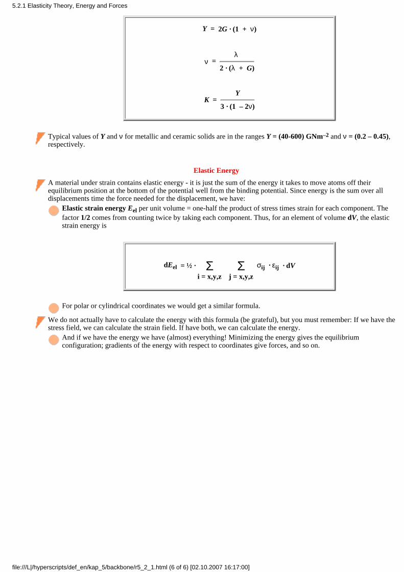
Y = 2G · (1 + ν)
ν = λ
2 · (λ + G)
K = Y
3 · (1 – 2ν)
Typical values of Y and ν for metallic and ceramic solids are in the ranges Y = (40-600) GNm–2 and ν = (0.2 – 0.45),respectively.
Elastic Energy
A material under strain contains elastic energy - it is just the sum of the energy it takes to move atoms off theirequilibrium position at the bottom of the potential well from the binding potential. Since energy is the sum over alldisplacements time the force needed for the displacement, we have:
Elastic strain energy Eel per unit volume = one-half the product of stress times strain for each component. Thefactor 1/2 comes from counting twice by taking each component. Thus, for an element of volume dV, the elasticstrain energy is
dEel = ½ · Σi = x,y,z
Σj = x,y,z
σij · εij · dV
For polar or cylindrical coordinates we would get a similar formula.
We do not actually have to calculate the energy with this formula (be grateful), but you must remember: If we have thestress field, we can calculate the strain field. If have both, we can calculate the energy.
And if we have the energy we have (almost) everything! Minimizing the energy gives the equilibriumconfiguration; gradients of the energy with respect to coordinates give forces, and so on.
5.2.1 Elasticity Theory, Energy and Forces
file:///L|/hyperscripts/def_en/kap_5/backbone/r5_2_1.html (6 of 6) [02.10.2007 16:17:00]

5.2.2 Stress Field of a Straight Dislocation
Screw Dislocation
The elastic distortion around a straight screw dislocation of infinite length can be represented in terms of a cylinderof elastic material deformed as defined by Volterra. The following illustration shows the basic geometry.
A screw dislocation produces the deformation shown in the left hand picture. This can be modeled by theVolterra deformation mode as shown in the right hand picture - except for the core region of the dislocation, thedeformation is the same. A radial slit was cut in the cylinder parallel to the z-axis, and the free surfacesdisplaced rigidly with respect to each other by the distance b, the magnitude of the Burgers vector of the screwdislocation, in the z-direction.In the core region the strain is very large - atoms are displaced by about a lattice constant. Linear elasticitytheory thus is not a valid approximation there, and we must exclude the core region. We then have no problemin using the Volterra approach; we just have to consider the core region separately and add it to the solutionsfrom linear elasticity theory.
The elastic field in the dislocated cylinder can be found by direct inspection. First, it is noted that there are nodisplacements in the x and y directions, i.e. ux = uy = 0 .
In the z-direction, the displacement varies smoothly from 0 to b as the angle θ goes from 0 to 2π. This can beexpressed as
uz = b · θ
2π =
b
2π· tan–1(y/x) =
b
2π · arctan (y/x)
Using the equations for the strain we obtain the strain field of a screw dislocation:
εxx = yy = εzz = εxy = εyx = 0
εxz = εzx = – b
4π ·
y
x2 + y2 = –
b
4π ·
sin θ
r
εyz = εzy = b
4π ·
x
x2 + y2 =
b
4π ·
cos θ
r
The corresponding stress field is also easily obtained from the relevant equations:
5.2.2 Stress Field of a Straight Dislocation
file:///L|/hyperscripts/def_en/kap_5/backbone/r5_2_2.html (1 of 4) [02.10.2007 16:17:00]

σxx = σyy = σzz = σxy = σyx = 0
σxz = σzx = – G · b
2π ·
y
x2 + y2 = –
G · b
2π ·
sin θ
r
σyz = σzy = G · b
2π ·
x
x2 + y2 =
G · b
2π ·
cos θ
r
In cylindrical coordinates, which are clearly better matched to the situation, the stress can be expressed via thefollowing relations:
σrz = σxy cosθ + σyz sinθ
σθ z = – σxz sinθ + σyz cosθ
Similar relations hold for the strain. We obtain the simple equations:
εθ z = εzθ = b
4πr
σθ z = σzθ = G · b
2πr
The elastic distortion contains no tensile or compressive components and consists of pure shear. σzθ acts parallel tothe z axis in radial planes of constant θ and σθz acts in the fashion of a torque on planes normal to the axis. The fieldexhibits complete radial symmetry and the cut thus can be made on any radial plane θ = constant. For a dislocationof opposite sign, i.e. a left-handed screw, the signs of all the field components are reversed.There is, however, a serious problem with these equations:
The stresses and strains are proportional to 1/r andtherefore diverge to infinity as r → 0 as shown in theschematic picture on the left.This makes no sense and therefore the cylinder used for thecalculations must be hollow to avoid r - values that are toosmall, i.e. smaller than the core radius r0.
Real crystals, of course, do (usually) not contain hollowdislocation cores. If we want to include the dislocationcore, we must do this with a more advanced theory ofdeformation, which means a non-linear atomistic theory.There are, however, ways to avoid this, provided one iswilling to accept a bit of empirical science.The picture simply illustrates that strain and stress are, ofcourse, smooth functions of r. The fact that linear elasticitytheory can not cope with the core, does not mean that thereis a real problem.
5.2.2 Stress Field of a Straight Dislocation
file:///L|/hyperscripts/def_en/kap_5/backbone/r5_2_2.html (2 of 4) [02.10.2007 16:17:00]

How large is radius r0 or the extension of the dislocation core? Since the theory used is only valid for small strains,we may equate the core region with the region were the strain is larger than, say, 10%. From the equations above itis seen that the strain exceeds about 0,1 or 10% whenever r ≈ b. A reasonable value for the dislocation core radiusr0 therefore lies in the range b to 4b, i.e. r0 ≥ 1 nm in most cases.
Edge Dislocation
The stress field of an edge dislocation is somewhat more complex than that of a screw dislocation, but can also berepresented in an isotropic cylinder by the Volterra construction.
Using the same methodology as in the case of a screw dislocation, we replace the edge dislocation by theappropriate cut in a cylinder. The displacement and strains in the z-direction are zero and the deformation isbasically a "plane strain".It is not as easy as in the case of the screw dislocation to write down the strain field, but the reasoning followsthe same line of arguments. We simply look at the results:
σxx = – D · y 3x2 + y2
(x2 + y2)2
σyy = D · y x2 – y2
(x2 + y2)2
σxy = σyx = D · xx2 – y2
(x2 + y2)2
σzz = ν · (σxx + σyy)
σzz = σzx = σyz = σzy = 0
We used the abbreviation D = Gb /2π (1 – ν) .
The stress field has, therefore, both dilational and shear components. The largest normal stress is σxx which actsparallel to the Burgers vector. Since the slip plane can be defined as y = 0, the maximum compressive stress (σxx isnegative) acts immediately above the slip plane and the maximum tensile stress (σxx is positive) acts immediatelybelow the slip plane.
The effective pressure (given by the sum over the normal components of the stress) is
p = 2 · (1 + ν) · D
3 ·
y
x2 + y2
We thus have compressive stress above the slip plane and tensile stresses below - just as deduced from thequalitative picture of an edge dislocation; graphical representation of the stress field of an edge dislocation isshown in the link.
For edge dislocations (and screw dislocations too), the sign of the stress- and strain components reverses if the sign ofthe Burgers vector is reversed.
Again, we have to leave out the dislocation core; the core radius again can be taken to be about 1b - 4b
5.2.2 Stress Field of a Straight Dislocation
file:///L|/hyperscripts/def_en/kap_5/backbone/r5_2_2.html (3 of 4) [02.10.2007 16:17:00]

We are left with the case of a mixed dislocation. This is not a problem anymore. Since we have a linear isotropictheory, we can just take the solutions for the edge- and screw component of the mixed dislocation and superimpose,i.e. add them.
As far as "simple" elasticity theory goes, we now have everything we can obtain. If better descriptions are needed,the matter becomes extremely complicated! But thankfully, this simple description is sufficient for mostapplications.
5.2.2 Stress Field of a Straight Dislocation
file:///L|/hyperscripts/def_en/kap_5/backbone/r5_2_2.html (4 of 4) [02.10.2007 16:17:00]

5.2.3 Energy of a Dislocation
With the results of the elasticity theory we can get approximate formulas for the line energy of a dislocation and the elastic interaction with otherdefects, i.e. the forces acting on dislocations.
The energy of a dislocation comes from the elastic part that is contained in the elastically strained bonds outside the radius r0 and from theenergy stored in the core, which is of course energy sitting in the distorted bonds, too, but is not amenable to elasticity theory.The total energy per unit length Eul is the sum of the energy contained in the elastic field, Eel, and the energy in the core, Ecore.
Eul = Eel + Ecore
Do not confuse energies E with Youngs modulus Y which is often (possibly here) written as E, too! From the context it is always clear what ismeant.Using the formula for the strain energy for a volume element given before, integration over the total volume will give the total elastic energy Eelof the dislocation. The integration is easily done for the screw dislocation; in what follows the equations are always normalized to a unit oflength.
dEel(screw) = π · r · dr · (σΘ z · εΘ z + σzΘ · εzΘ ) = 4π · r · dr · G · (εΘ z)2
Eel(screw) = G · b2
4π ·
R⌠⌡ro
dr
r =
G · b2
4π · ln
R
ro
The integration runs from r0, the core radius of the dislocation to R, which is some as yet undetermined external radius of the elastic cylindercontaining the dislocation. In principle, R should go to infinity, but this is not sensible as we are going to see.
The integration for the edge dislocation is much more difficult to do, but the result is rather simple, too:
Eel(edge) = G · b2
4π(1 – ν) · ln
R
ro
So, apart from the factor (1 – ν), this is the same result as for the screw dislocation.
Let us examine these equations. There are a number of interesting properties; moreover, we will see that there are very simple approximations to begained:1. The total energy U of a dislocation is proportional to its length L.
U = Eul · L = L · (Eel + Ecore)
Since we always have the principle of minimal energy (entropy does not play a role in this case), we can draw a important conclusion:
A dislocation tends to be straight between its two "end points" (usually dislocation knots). That is a first rule about the direction a dislocationlikes to assume.
2. The line energy of an edge dislocation is always larger than that of a screw dislocation since (1 – ν) < 1. With ν ≈ 1/3, we have Escrew ≈ 0,66·Eedge.
This means that a dislocation tends to have as large a screw component as possible. This is a second rule about the direction a dislocation likes toassume which may be in contradiction to the first one. It is quite possible that a dislocations needs to zig-zag to have as much screw character asgeometrially allowed - it then cannot be straight at the same time.
3. The elastic part of the energy depends (logarithmically) on the crystal size (expressed in R), for an infinite crystal it is infinite (∞)! Does this makeany sense?
Of course this doesn't make sense. Infinite crystals, however, do not make sense either. And in finite crystals, even in big finite crystals, theenergy is finite!Moreover, in most real crystals it is not the outer dimension that counts, but the size of the grains which are usually quite small. In addition, ifthere are many dislocations with different signs of the Burgers vector, their strain fields will (on average) tend to cancel each other. So forpractical cases we have a finite energy.
4. The elastic part of the energy also depends (logarithmically) on the core radius r0.
5. The energy is a weak function of the crystal (or grain size) R.
Taking an extremely small value for r0, e.g. 0,1 nm, we obtain for ln (R/r0) an extreme range of 20,7 - 2,3 if we pick extreme values for R of 100mm or 1 nm, respectively. A more realistic range for R would be 100 µm - 10 nm, giving ln (R/r0) = 13,8 - 4,6. Grain size variations, withinreasonable limits, thus only provide a factor of 2 - 3 for energy variations.
5.2.3 Energy of a Dislocation
file:///L|/hyperscripts/def_en/kap_5/backbone/r5_2_3.html (1 of 3) [02.10.2007 16:17:00]

We will now deduce an approximation for the line energy that is sufficiently good for most purposes.
We equate r0 with the magnitude of the Burgers vector, |b|. This makes sense because the Burgers vector is a direct measure of the "strength" of adislocation, i.e. the strength of the displacement in the core region.We need a value for the energy in the core of the dislocations, which so far we have not dealt with. Since there is no easy way of calculating thatenergy, we could equate it in a first approximation with the energy of melting. That would make sense because the dislocation core is comparablein its degree of distortion to the liquid state. More sophisticated approaches end up with the best simple value:
Ecore = G · b2
2π
There are, however, other approaches, too.
The total energy for r0 = b then becomes
Etot = G · b2
4π ·
lnR
b + 2
More generally, the following formula is often used
Etot = G · b2
4π(1 – ν) ·
lnR
b + B
with B = pure number best approximating the core energy of the particular case. Often B = 1 is chosen, leading to
Etot = G · b2
4π(1 – ν) ·
lnR
b + 1
= G · b2
4π(1 –ν ) ·
lne ·R
b
For the last equation bear in mind that ln(e) = 1.
The ln term is not very important. To give an example; it is exactly 4π for e · R = 3,88 x 10⁴ |b|, i.e. for R ≈ 5 µm; the total energy in this case wouldbe Etot = 2G · b2.
In a very general way we can write
Etot = α · G · b2
And α (from measurements) is found to be α ≈ 1,5 ....0,5. If we do not care for factors in the order of unity, we get the final very simple formulafor the line energy of a dislocation
Etotal ≈ G · b2
With this expression for the line energy of a dislocation, we can deduce more properties of dislocations.
6. Dislocations always tend to have the smallest possible Burgers vector.
Since for Burgers vectors bi larger than the smallest translation vector of the lattice and thus expressible by bi = b1 + b2 ; b1,2 = some shortervectors of the lattice, we always have
5.2.3 Energy of a Dislocation
file:///L|/hyperscripts/def_en/kap_5/backbone/r5_2_3.html (2 of 3) [02.10.2007 16:17:00]

(b1)2 + (b2)2 < b2
A splitting into smaller Burgers vectors is therefore always energetically favorable.
There are therefore no dislocations with large Burgers vectors!
If a dislocation would have a large Burgers vector, it would immediately split into two (or more) dislocations with smaller Burgers vectors.
This is always possible, because in the Volterra construction you can always replace one cut with the translation vector b by two cuts with b1 andb2 so that b = b1 + b2.
7. The line energy is in the order of 5 eV per Burgers vector..
This makes dislocations automatically non-equilibrium defects. They will not come into being out of nothing like point defects for free enthalpyreasons.
8. The line energy ( = energy per length) has the same dimension as a a force, it expresses a line tension, i.e. a force in the direction of the line vectorwhich tries to shorten the dislocation.
It actually is a force, as we can see from the definition of such a line tension F:
F = – dU
dL
We thus may imagine a dislocation as a stretched rubber band, which tries to be as short as possible. But one should be careful not to overreachthis analogy. Ask yourself: What keeps dislocations loops stable?
5.2.3 Energy of a Dislocation
file:///L|/hyperscripts/def_en/kap_5/backbone/r5_2_3.html (3 of 3) [02.10.2007 16:17:00]

5.2.4 Forces on Dislocations
Again, detailed calculations are complicated and must be done numerically in most cases. For practicalusage, however, we will find simple approximations by using the energy formula already derived; thiswill be good enough for most cases.
First, we have to see that for the movement of a dislocation on its glide plane, we only need toconsider the shear stress on this plane. This is so, because only force components lying in the glideplane of the dislocation can have any effect on dislocation motion in the glide plan. The normalcomponents of the the stress in the glide plane system act perpendicular to the glide plane and thuswill not contribute to the dislocation movement.Both shear stress components in the glide plane act on the dislocation. Important, however, is onlytheir combined effect in the direction of the Burgers vector, which is called the resolved shearstress τres.
However, while the resolved shear stress points into the direction of the Burgers vector, thedirection of the force component acting on, i.e. moving the dislocation, is always perpendicular tothe line direction! This is so because the force component in the line direction does not do anything- a dislocation cannot move in its own direction. or, if you like that better: If it would - nothinghappens! The whole situation is outlined below
Under the influence of the force F acting on the dislocation and which we want to calculate, thedislocation moves and work W is done given by W = Force · distance. Lets look at the ultimate workthat can be done by moving one dislocation.
If the dislocation moves in total through the crystal on a glide plane with the area A, the upper halfof the crystal moves by b relative to the lower half which is the distance on which work has beendone.This only happens if a shear force acts on the crystal, and this force obviously does some work W.This work is done bit by bit by moving the dislocation through the crystal, so we must identify theforce that does work with the force F acting on the dislocation.
The acting shear stress in this case is then τ = Force F/area A. and force F is that component of theexternal force that is contained or "resolved" in the glide plane of the dislocation as discussedabove.
For the total work W done by moving half of the crystal a distance equal to the Burgers vector b weobtain
W = A · τ · b
With A · τ = Force; b = Burgesvector = distance.
5.2.4 Forces on Dislocations
file:///L|/hyperscripts/def_en/kap_5/backbone/r5_2_4.html (1 of 5) [02.10.2007 16:17:01]

We just as well can divide W into incremental steps dW, the incremental work done on an incrementalarea that consists of an incremental piece dl of the dislocation moving an incremental distance ds, asshown below
The relation between the incremental work dW to the total work W then is just the ratio between theincremental area to the total area; we have
dW
W =
ds · dl
A
Putting everything together, we obtain
dW = A · τ · b ·dl · ds
A= τ · b · dl · ds
An incremental piece of work dW can always be expressed as a force times an incremental distanceds; i.e. dW = F · ds. The force F acting on the incremental length dl of dislocation then obviouslyis F = τ · b · dl.If we now redefine the force on a dislocation slightly and refer it to the (incremental) unit length dl,i.e. we take F* = F/dl, we obtain a very simple formula for the magnitude of the force (it is not avector!) acting on a unit length of a dislocation:
F* = τ · b
This is easy - but beware of the sign of the force! You must get all the signs right (Burgers vector, linevector, τ) to get the correct sign of the force! We also will drop the "*" in what follows, because as withall other properties of dislocations, it is automatically per unit length if not otherwise specified.
5.2.4 Forces on Dislocations
file:///L|/hyperscripts/def_en/kap_5/backbone/r5_2_4.html (2 of 5) [02.10.2007 16:17:01]

The important part is τ. It is the component of the shear strain in the glide plane in the direction ofb. This is normally not a known quantity but must be calculated, e.g. by a coordinate transformationof a given external stress tensor to a coordinate system that contains the glide plane as one of itscoordinate planes.
Again, we must realize that the Force F as defined above is always perpendicular to the dislocation line;even if τ = constant everywhere on the glide plane.
This is somewhat counterintuitive, but always imagine the limiting case of a pure edge and screwdislocation: The same external τ must exert a force on a screw dislocation that is perpendicular tothe force on an edge dislocation to achieve the same deformation (think about that; looking at thepictures helps!)
This calls for a little exercise
Exercise 5.2-2
Forces on a dislocation
In reality, dislocations can rarely move in total because they are usually firmly anchored somewhere.For a straight edge dislocation anchored at two points (e.g. at immobile dislocation knots) responding toa constant τ, we have the following situation.
The forces resulting from the resolved shear stress (red arrows) will "draw out" the dislocation intoa strongly curved dislocation (on the right). A mechanical equilibrium will be established as soon asthe force pulling back the dislocation (its own line tension) exactly cancels the external force.The middle picture shows an intermediate stage where the dislocation is still moving.
It is possible to write down the force on a dislocation as a tensor equation which automatically takes careof the components - but this gets complicated:
First we need to express the force as a vector with components in the glide plane and perpendicularto it. We define F = Force on a dislocation = (FN, FG)
With FG = component in the glide plane, FN = component vertical to the glide plane. Only FG is ofinterest, it is given by
5.2.4 Forces on Dislocations
file:///L|/hyperscripts/def_en/kap_5/backbone/r5_2_4.html (3 of 5) [02.10.2007 16:17:01]
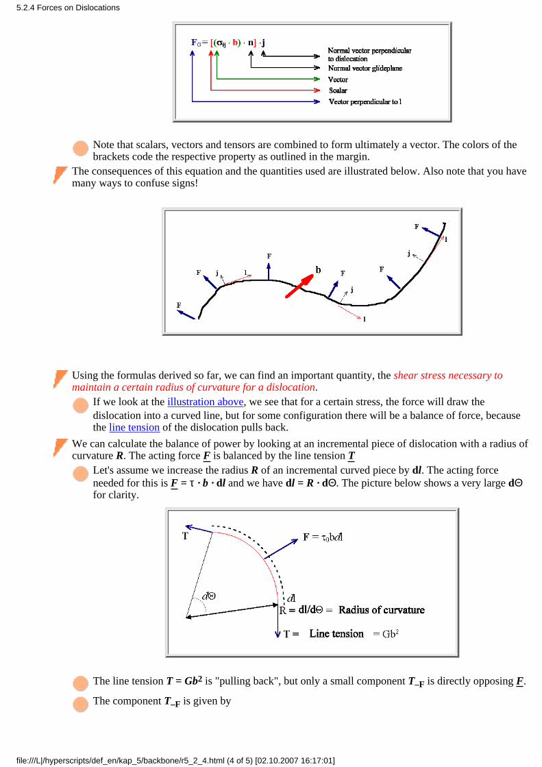
Note that scalars, vectors and tensors are combined to form ultimately a vector. The colors of thebrackets code the respective property as outlined in the margin.
The consequences of this equation and the quantities used are illustrated below. Also note that you havemany ways to confuse signs!
Using the formulas derived so far, we can find an important quantity, the shear stress necessary tomaintain a certain radius of curvature for a dislocation.
If we look at the illustration above, we see that for a certain stress, the force will draw thedislocation into a curved line, but for some configuration there will be a balance of force, becausethe line tension of the dislocation pulls back.
We can calculate the balance of power by looking at an incremental piece of dislocation with a radius ofcurvature R. The acting force F is balanced by the line tension T
Let's assume we increase the radius R of an incremental curved piece by dl. The acting forceneeded for this is F = τ · b · dl and we have dl = R · dΘ. The picture below shows a very large dΘfor clarity.
The line tension T = Gb2 is "pulling back", but only a small component T–F is directly opposing F.
The component T–F is given by
5.2.4 Forces on Dislocations
file:///L|/hyperscripts/def_en/kap_5/backbone/r5_2_4.html (4 of 5) [02.10.2007 16:17:01]

T = T · sin(dΘ/2) ≈ dΘ/2 for small dΘ
Since there are two components we have the balance of power
T · dΘ = Gb2· dΘ = τ · b · dl = τ · b ·R · dΘ
The equilibrium radius R0 obtained for a shear stress τ0 is thus
R0 = Gb
τ0
This will have important consequences becuase the equation states that a dislocation will move"forever" if τ > Gb/Rmin with Rmin denoting some minimal radius of curvature that cannot bedecreased anymore.
From looking at force balance, we now can answer the questions posed before for a dislocation network:
The sum of the line tensions at a knot must be zero, too (or at least very small), otherwise the knotand the dislocations with it will move. We thus expect that 3-knots will always show angles of(approximately) 120o.
Knots with more than three dislocations will, as a rule, split into 3-knots, since otherwise there canbe no easy balance of line tensions. In real cases, however, you must also consider the geometry ofthe anchor points (are they fixed, can they move?), the change of line energy with the character ofthe dislocation and the new total length of the dislocations.
5.2.4 Forces on Dislocations
file:///L|/hyperscripts/def_en/kap_5/backbone/r5_2_4.html (5 of 5) [02.10.2007 16:17:01]

5.2.5 Interactions Between Dislocations
We will first investigate the interaction between two straight and parallel dislocations of the same kind.
If we start with screw dislocations, we have to distinguish the following cases:
In analogy, we next must consider the interaction of edge dislocations, of edge and screw dislocationsand finally of mixed dislocations.
The case of mixed dislocations - the general case - will again be obtained by considering theinteraction of the screw- and edge parts separately and then adding the results.
With the formulas for the stress and strain fields of edge and screw dislocations one can calculate theresolved shear stress caused by one dislocation on the glide plane of the other one and get everythingfrom there.But for just obtaining some basic rules, we can do better than that. We can classify some basic caseswithout calculating anything by just exploiting one obvious rule:
The superposition of the stress (or strain) fields of two dislocations that are moved toward eachother can result in two basic cases:1. The combined stress field is now larger than those of a single dislocation. The energy of theconfiguration than increases and the dislocations will repulse each other. That will happen ifregions of compressive (or tensile) stress from one dislocation overlaps with regions of compressive(or tensile) stress from the other dislocation.2. If the combined stress field is lower than that of the single dislocation, they will attract eachother. That will happen if regions of compressive stress from one dislocation overlaps with regionsof tensile stress from the other dislocation
This leads to some simple cases (look at the stress / strain pictures if you don't see it directly)
1. Arbitrarily curved dislocations with identical b on the same glide plane will always repel eachother.
5.2.5 Interactions Between Dislocations
file:///L|/hyperscripts/def_en/kap_5/backbone/r5_2_5.html (1 of 3) [02.10.2007 16:17:01]

2. Arbitrary dislocations with opposite b vectors on the same glide plane will attract and annihilateeach other
Edge dislocations with identical or opposite Burgers vector b on neighboring glide planes mayattract or repulse each other, depending on the precise geometry. The blue double arrows in thepicture below thus may signify repulsion or attraction.
The general formula for the forces between edge dislocations in the geometry shown above is
Fx = Gb2
2π(1 –ν) ·
x · (x2 – y2)
(x2 + y2)2
Fy = Gb2
2π(1 –ν) ·
y · (3x2 + y2)
(x2 + y2)2
For y = 0, i.e. the same glide plane, we have a 1/x or, more generally a 1/r dependence of the forceon the distance r between the dislocations.For y < 0 or y > 0 we find zones of repulsion and attraction. At some specific positions the force iszero - this would be the equilibrium configurations; it is shown below.The formula for Fy is just given for the sake of completeness. Since the dislocations can not movein y-direction, it is of little relevance so far.
5.2.5 Interactions Between Dislocations
file:///L|/hyperscripts/def_en/kap_5/backbone/r5_2_5.html (2 of 3) [02.10.2007 16:17:01]

The illustration in the link gives a quantitative picture of the forces acting on one dislocation on its glideplane as a function of the distance to another dislocation.
5.2.5 Interactions Between Dislocations
file:///L|/hyperscripts/def_en/kap_5/backbone/r5_2_5.html (3 of 3) [02.10.2007 16:17:01]

5.3 Movement and Generation of Dislocations
5.3.1 Kinks and Jogs
Kinks in Dislocations
In most crystals and under most circumstances there is no such thing as a straight dislocation. Realdislocations contain kinks and jogs - sudden deviations from a straight line on atomic dimensions.These defects within a defect may strongly influence the mobility of dislocations and are thus ofimportance.
They owe their existence first of all to the fact that dislocations always "live" in a crystals - in aperiodic arrangement of atoms. We have not used that fact so far, except in a rather abstract way forthe very definition of dislocations with the Volterra cut. Now it is time to appreciate the effects ofthe crystal on the fine structure of dislocatons.Kinks (and jogs) may be produced by several mechanisms, in particular they may be formed by themovement of the dislocation.
First, let's look at kinks. For that we first have to consider the concept of the Peierls potential of adislocation.
Consider the movement of an edge dislocation as shown below. The green circles symbolize thelast atom on the inserted half- plane of an edge dislocation. In local equilibrium its distance to theatoms to the left or right will be same for basic reasons of symmetry, cf. the perspective drawing ofan edge dislocation.
If the dislocation is to move, the last atom (and the ones above to some extent) has to press againstthe neighboring atom on one side and move away from the atom on the other side. That is clearly asituation with a higher energy which can be cast into a potential energy curve as shown in theillustration. At some point when both lattice plans are most affected, there is a maximum and a newminimum as soon as the dislocation has moved by one Burgers vector. The minima and maxima ofthis Peierls potential are along directions of high symmetry.To overcome the maximum of the Peierls potential, the stress has to be larger than some intrinsiccritical shear stress τcrit.
The Peierls potential defines special low-energy directions in which the dislocation prefers to lie. This isthe third rule for directions that dislocations like to assume! (Try to remember the first and second rule,or use the links).
In other words, the inserted half-plane for the easy-to-imagine case of an edge dislocation should beclearly defined and should be in a symmetric position between its neighbour planes - exactly as wealways have drawn it.A dislocation that is almost, but not quite an edge dislocation, thus would prefer to be a pure edgedislocation over long distances and concentrate the "non-edginess" in small parts of its length asshown below. The same is true for screw dislocations, even so it is not quite as easy to contemplate.
5.3.1 Movement of Dislocations
file:///L|/hyperscripts/def_en/kap_5/backbone/r5_3_1.html (1 of 5) [02.10.2007 16:17:01]

The dislocation runs in the minima of the Peierls potential as long as possible and then crosses overbriskly when it has to be. The transition from one Peierls minimum to the next one is called a kinkas shown in the picture above.
The kinks that come into existence in this way are called geometric kinks. But there is also a secondkind, the thermal equilibrium (double)-kink, i.e. a crossing over to a neighboring Peierls valleyfollowed by a "jump" back.
A kink, or better a double-kink, is simply a defect in an otherwise straight dislocation line, addingsome energy and entropy. Since the formation energy of a double kink is not too large, they willbe present in thermal equilibrium with concentrations following a standard Boltzmanndistribution.To make that perfectly clear: While a dislocation by itself is never in thermal equilibrium, i.e. willnever form spontaneously by thermal activation, this is not true for the defects it may contain.Double-kinks, seen as defects in a dislocation line, form and disappear spontaneously, if sufficientthermal energy is available; their number or density thus will follow a Boltzmann distribution.Once a thermal double-kink has been formed, the two single kinks may move apart; if the process isrepeated, we have a new mode of dislocation movement for an otherwise perhaps immobiledislocation. This is shown below.
Kinks then are steps of atomic dimension in the dislocation line that are fully contained in the glideplane of the dislocation
With this general definition, we can consider kinks in all dislocations, not just edge dislocations.
Screw dislocations have a Peierls potential, too, and thus they may contain kinks. The kink, perdefinition, is then a very short a piece of dislocation with edge character.
This has far reaching consequences: A screw dislocation with a kink now either has a specific glideplane - the glide plane of the kink - or the kink is an anchor point for the screw dislocation.Kinks can do more: As indicated above, at not too low temperatures when the generation of thermaldouble kinks becomes possible, the applied stress may be below the critical shear stress needed tomove the dislocation in toto (i.e. move it across the Peierls potential), but might be large enough toseparate double kinks and thus promote dislocation movement and plastic deformation. We haveone of several effects here that make crystals "softer" at high temperatures.
5.3.1 Movement of Dislocations
file:///L|/hyperscripts/def_en/kap_5/backbone/r5_3_1.html (2 of 5) [02.10.2007 16:17:01]

The best way to investigate kinks are internal friction experiments.
An oscillating deformation is chosen, e.g. by vibrating a thin specimen driven by anelectromagnetic field. The amplitude and thus the internal stress and strain are easily measured. Aslong as the stress is not too large, deformation proceeds by the generation and the movement ofkinks. This is a fully reversible process and the response to an external stress thus is purely elasticeven though a dislocation moved!However, in contrast to elasticity just coming from stretching the bonds between the atoms, thegeneration and movement of double kinks takes time and is strongly temperature dependent.Specific time constants are involved and a peculiar frequency dependence of the elastic responsewill be observed which contains information about the kinks. More about internal friction in thelink.
Jogs in Dislocations
The term "Jogs" is sometimes considered to be the term for all "breaks" or steps in a dislocation linewith atomic dimensions. Kinks then would be a subclass of jogs with the speciality of being in the glideplane.
However, it is customary to use the term "jogs" for all steps that are not contained in the glideplane. Looking just at the inserted half-plane of an edge dislocation, jogs and kinks would look likethis:
But remember: Jogs and kinks can occur in any dislocation, not just edge dislocations - they are justnot as easily drawn!
Jogs in edge dislocations are obviously prime places for the emission or absorption of point defects as isshown in the next illustration which looks at the inserted half-plane of an edge dislocation.
5.3.1 Movement of Dislocations
file:///L|/hyperscripts/def_en/kap_5/backbone/r5_3_1.html (3 of 5) [02.10.2007 16:17:01]

The movement of jogs by emission or absorption of point defects means that the dislocation moves.This particular process of dislocation movement is called climb of dislocations. It is a movementthat does not take place in the glide plane of the dislocation.
Generally speaking, we define:
Conservative movement of dislocations = movement in the glide plane = glide (for short) =movement without assistance of point defects. Non conservative movement of dislocations = movement not in the glide plane = climb (forshort) = movement needing the assistance of point defects.
Generation of Kinks and Jogs
How do kinks and jogs come into existence? Three mechanisms can be identified.
Thermally activated generation of double kinks as discussed above.
Thermally induced generation of jogs by absorption or emission of point defects. This mechanismis thermally induced (and not "activated") because it responds to a super- or undersaturation ofpoint defects. At large under- or supersaturations, the process becomes more likely. Here we haveone of the source/sink processes needed for point defect equilibrium.
Intersection of dislocations
The last process is new and needs some explanation. Lets look at the movement of an edge dislocationin the following geometry:
The intersection of the edge dislocation with the screw dislocation produces one jog each perdislocation. (Consider the cut-and-move procedure and you will see why). It is clear that the samething happens for the intersection of arbitrary mixed dislocations - a jog characterized by theBurgers vector of the dislocation that moved across will be generated.
This gives us a general relation and explains to some extent why plastic deformation is an extremely nonlinear process:
Movement of dislocations generates jogs.
Jogs influence severely the movement of dislocations - so there is some feedback in the process ofplastic deformation, and feedback of any kind is the hallmark of non-linear processes.
Considering jogs and kinks (together with knots), we start to consider real dislocations - and its gettingcomplicated.
And don't forget: All those great electron microscope pictures showing all kinds of dislocations,never show the jogs and kinks! They are simply too small. So even dislocation that look like perfectstraight lines in a TEM picture, may be full of jogs and kinks.
There is one last property induced by these defects in a defect:
5.3.1 Movement of Dislocations
file:///L|/hyperscripts/def_en/kap_5/backbone/r5_3_1.html (4 of 5) [02.10.2007 16:17:01]

Jogs, kinks and their combinations may produce "debris" left behind by a moving dislocation,because it is often "better" for dislocations to tear away from immobile parts like jogs, leavingbehind a trail of point defects which in turn may agglomerate.If the jog is large extending over several lattice planes, a whole trail of small dislocation loops mayform. The formation of a trail of vacancies in the wake of a jogged moving screw dislocation isillustrated in the link
Some more text to come - but try the exercise anyway!
Exercise 5.3-1
Forces on a dislocation
5.3.1 Movement of Dislocations
file:///L|/hyperscripts/def_en/kap_5/backbone/r5_3_1.html (5 of 5) [02.10.2007 16:17:01]

5.3.2 Generation of Dislocations
Whereas we now learned a little bit about the complications that may occur when dislocations move, wefirst must have some dislocations before plastic deformation can happen. In other words: We needmechanisms that generate dislocations in the first place!
Of course, dislocations can just be generated at the surface of the crystal; the simple picturesshowing plastic deformation by an (edge) dislocation mechanism give an idea how this mayhappen. But more important are mechanisms that generate dislocations in the bulk of a crystal. Themost important mechanism is the Frank-Read mechanism shown below.
We have asegment ofdislocationfirmlyanchored attwo points(red circles).The force F =b · τres isshown by asequence ofarrowsThedislocationsegmentresponds tothe force bybowing out. Ifthe force islarge enough,the criticalconfigurationof a semicirclemay bereached. Thisrequires amaximumshear stress ofτmax = Gb/R
If the shearstress is higherthan Gb/R, theradius ofcurvature istoo small tostop furtherbowing out.Thedislocation isunstable andthe followingprocess nowproceedsautomaticallyand quickly.
5.3.2 Generation of dislocations
file:///L|/hyperscripts/def_en/kap_5/backbone/r5_3_2.html (1 of 4) [02.10.2007 16:17:02]

The twosegmentsshortly beforethey touch.Since the twoline vectors atthe point ofcontact haveopposite signs(or, if youonly look atthe two partsalmosttouching: theBurgersvectors havedifferent signsfor the sameline vectors),the segmentsin contact willannihilateeach other.Theconfigurationshown is whatyou haveimmediatelyafter contact;it is totallyunstable (thinkof the rubberband model!).It willimmediatelyform a straightsegment and a"nice"dislocationloop whichwill expandunder theinfluence ofthe resolvedshear stress.
5.3.2 Generation of dislocations
file:///L|/hyperscripts/def_en/kap_5/backbone/r5_3_2.html (2 of 4) [02.10.2007 16:17:02]

The regainedold segmentwillimmediatelystart to gothrough thewhole processagain, andagain, andagain, ... - aslong as theforce exists. Awholesequence ofnesteddislocationloops will beproduced.Stableconfigurationafter theprocess. Theloop is free tomove, i.e.grow muchlarger underthe appliedstress. It willencounterotherdislocations,form knotsand becomepart of anetwork. Thenext loop willfollow and soon - as long asthere isenough shearstress.
The Frank-Read process, although looking a bit odd, will occur many times under sufficient load. It canproduce any density of dislocations in short times, because the newly formed dislocations will move,become anchored at some points, and start to generate Frank-Read loops, too.
Of course, Frank-Read dislocation sources can also be stopped - e.g. by cutting through thegenerating dislocation by another dislocation. We thus will have a certain finite dislocation densityunder certain external conditions. It may, however, depend on many parameters, including thehistory of the material.Some kind of Frank-Read mechanism may also operate from irregularities on the surface (externalor internal), an example of such a source is shown in the X-ray topography below.
5.3.2 Generation of dislocations
file:///L|/hyperscripts/def_en/kap_5/backbone/r5_3_2.html (3 of 4) [02.10.2007 16:17:02]

This picture comes from the work of K.B. Kostin (a former student in Kiel) together with manyothers in St. Petersburg. It is a result of investigations into "wafer bonding", where to Si wafers areplaced on top of each other and "bonded", so that a single piece of Si results - with a grain boundaryin between. The mottled area in the upper left hand corner shows such a bonded structure, whereasthe dark area containing the dislocations as white lines, remained unbonded.Dislocations were introduced into one of the wafers and one point on the edge of the bonded areaacted as a Frank-Read source. The nested series of dislocation loops is splendidly visible. There arealso lots of straight dislocations which have moved considerable distances from their point oforigin.
How else can we make dislocations? Suffice it to mention that there are variants of the basic Frank-Readmechanism, too and some more exotic mechanisms. We will not go into details; the important part isthat it is generally an easy process to generate many dislocations provided you already have a few tostart with.
Last but not least: "Frank" is not the first name of Mr. Read - as ever so often, two independentpersons figured out this mechanism at practically the same time (in 1950) - look up the link fordetails.
5.3.2 Generation of dislocations
file:///L|/hyperscripts/def_en/kap_5/backbone/r5_3_2.html (4 of 4) [02.10.2007 16:17:02]
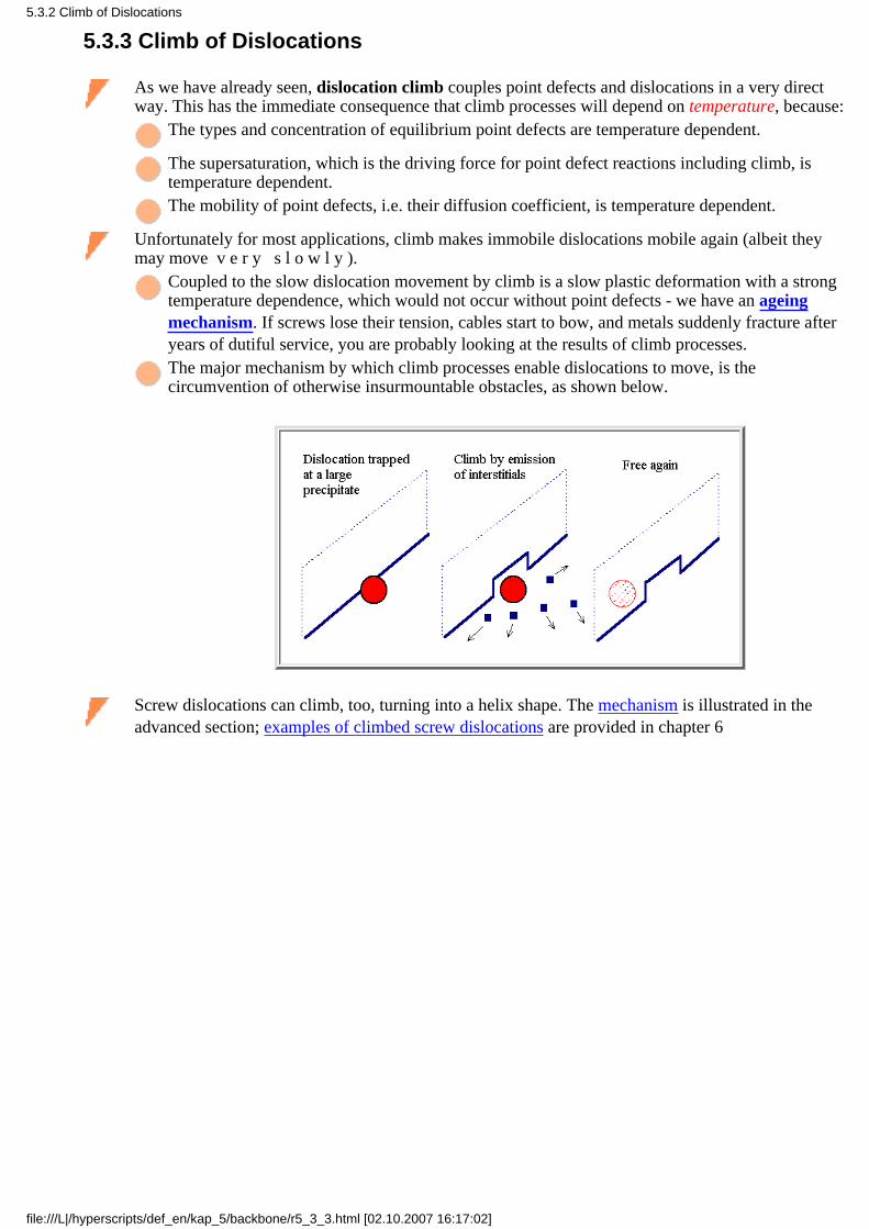
5.3.3 Climb of Dislocations
As we have already seen, dislocation climb couples point defects and dislocations in a very directway. This has the immediate consequence that climb processes will depend on temperature, because:
The types and concentration of equilibrium point defects are temperature dependent.
The supersaturation, which is the driving force for point defect reactions including climb, istemperature dependent.The mobility of point defects, i.e. their diffusion coefficient, is temperature dependent.
Unfortunately for most applications, climb makes immobile dislocations mobile again (albeit theymay move v e r y s l o w l y ).
Coupled to the slow dislocation movement by climb is a slow plastic deformation with a strongtemperature dependence, which would not occur without point defects - we have an ageingmechanism. If screws lose their tension, cables start to bow, and metals suddenly fracture afteryears of dutiful service, you are probably looking at the results of climb processes.The major mechanism by which climb processes enable dislocations to move, is thecircumvention of otherwise insurmountable obstacles, as shown below.
Screw dislocations can climb, too, turning into a helix shape. The mechanism is illustrated in theadvanced section; examples of climbed screw dislocations are provided in chapter 6
5.3.2 Climb of Dislocations
file:///L|/hyperscripts/def_en/kap_5/backbone/r5_3_3.html [02.10.2007 16:17:02]

5.4 Partial Dislocations and Stacking Faults
5.4.1 Stacking Faults and Close Packed Lattices
Stacking Faults and Frank Dislocations
Let's consider a close packed lattice, and look at the close packed planes.
In a simple model using perfect spheres we have the following situation:
We take the blue atoms as the base plane for what we are going to built on it, wewill call it the "A - plane".
The next layer will have the center of the atoms right over the depressions of the A -plane; it could be either the B - or C - configuration.
Here the pink layer is in the "B" position
If you pick the B - configuration (and whatever you pick at this stage, we can alwayscall it the B - configuration), the third layer can either be directly over the A - planeand then is also an A - plane (shown for one atom), or in the C - configuration.
If you chose "A"; you obtain the hexagonal close packed lattice (hcp), if you chose"C", you get the face centered cubic lattice (fcc)
You can't have it both ways. If you start in the C position somewhere (in the picturethe green atoms) and on the A position somewhere else (light blue), you will get aproblem as soon as the two layers meet.
For varieties sake, and to be able to distinguish the layers better, the bottom A layerhere is in dark blue.
The stacking sequences of the two close-packed lattices therefore are
fcc: ABCABCABCA...
hcp: ABABABA...
Looking at this sequences in cross-section is a bit more involved; it is best done in a <110> projection of the fcc lattice
Planes with the same letter areon lines perpendicular to the{111} planes, as indicated bythin black lines.
5.4.1 Partial Dislocations and Stacking Faults
file:///L|/hyperscripts/def_en/kap_5/backbone/r5_4_1.html (1 of 4) [02.10.2007 16:17:02]

The projection of the elementarycell is shown with red lines.We now remove parts of ahorizontal {111} plane - e.g. byagglomeration of vacancies onthat plane - it shall be a C-planehere.
Now A and C- planes becomeneighbors and relax into theconfiguration shown.We produced a stacking faultbecause the stacking sequenceABCABCA..has been changed to the faulty
sequence ABCABABCA...The stacking fault is between thelarge letters.Stacking faults by themselvesare simple two-dimensionaldefects. They carry a certainstacking fault energy γ; veryroughly around a few 100mJ/m2.The disc of vacancies obviouslyis bordered by an edgedislocation. What is the Burgersvector of this dislocation? Weshall see farther down.
If we do not condense vacancies on a plane, but fill in a disc of agglomerated interstitials, we obtain the following structure
The stacking sequenceABCABCA... again is faulty; it
is now ABCABACABCA....The stacking fault is between thelarge letters.This is a different kind ofstacking fault than the one fromabove.For historical reasons, we callthe stacking fault produced byvacancy agglomeration"intrinsic stacking fault" andthe stacking fault produced byinterstitial agglomeration"extrinsic stacking fault".The extrinsic stacking fault alsoseems to be bordered by an edgedislocation. Again, what is theBurgers vector?
In order to determine the Burgers vector of the apparent dislocations bordering the stacking faults, we must do a Burgers circuit or use the Volterradefinition. For this we must first be clear about the directions in the chosen projection. This is shown below.
5.4.1 Partial Dislocations and Stacking Faults
file:///L|/hyperscripts/def_en/kap_5/backbone/r5_4_1.html (2 of 4) [02.10.2007 16:17:02]

Directions in the <110> projectionshown for the elementary cell traced out on the right or above
Traces of the (color-coded) planes (right angle to direction)in the <110> projection and the elementary cell.
From a Burgers circuit or from a Voltaterra cut, we obtain the same result (Try it! It is easier in this case to hop from atom to atom (instead from latticepoint to lattice point); start at the stacking fault).
The Burgers vector of these dislocations is b = ± a/3 <111> - and this is not a translation vector of the fcc - lattice! Do not, at this point, forget thedistinction between lattice and crystal!
Dislocations with Burgers vectors of this type are called partial dislocations, or more correctly, Frank partial dislocations, or simply Frankdislocations.
This brings us to a general definition: Dislocations with Burgers vector that are not translation vectors of the lattice are called partial dislocations. Theymust by necessity border a two-dimensional defect, usually a stacking fault.
This can be verified with the Volterra construction if we add one element: Make a cut in a {111} plane and shift by a/3<111> perpendicular tothe plane. The element added is that we now include shift vectors that are not translation vectors of the lattice, but vectors between equivalentpositions of the atoms.Partial Burgers vectors and stacking faults thus may exist if the packing of atoms defining the crystal has additional symmetries not found in thelattice. Check this advanced module for an elaboration.
As stated in the definition of the Volterra cut-shift-weld procedure, you now must add or remove material. The total effect is the creation of aFrank partial along the cut line and, by necessity, a stacking fault on the cut part of the {111} plane.
We also see now that the primary defects which are generated by the agglomeration of intrinsic point defects in fcc lattices are small "stacking faultloops".
Shockley Dislocations
Now we may ask a question: Can we produce stacking faults without the participation of point defects? Indeed, we may - use the Volterra definition tosee how:
Make a cut on a {111} plane, e.g. between the A- and B-plane.
Move the B-plane so it is now in a C-position. No material must be removed or added.
Weld together: You now have the stacking sequence ABCACABCA... instead of ABCABCA.., i.e. you produced the stacking sequence of anintrinsic stacking fault.
The vector of the shift must be the Burgers vector of the partial dislocation resulting from this operation as the boundary of the intrinsic stacking fault.This shift vector can be seen by projecting the elementary cell on the close packed {111} plane where we did the cut.
The displacement vectorsfor producing stacking faults
with the Volterra construction.We have all vectors pointing
from one "dent" to a neighboring one.
The directions in the {111} plane.If you superimpose the two red circles,
you have the projection shown on the left.
Each one of the red vectors wouldmove a {111} plane from
an A-position to a B position(marked by a green dot).
The relevant displacement vectors are of the type b = a/6<112>. (Check it! It's good exercise for getting used to lattice projections). Dislocationswith this kind of Burgers vector are called Shockley partial dislocations, Shockley dislocations, or simply Shockley partials.In our <110> projection, Shockley and Frank partials look like this (after a picture from "Hull and Bacon"). The pictures are drawn in a slightlydifferent style, to make things a bit more complicated (get used to it!)
5.4.1 Partial Dislocations and Stacking Faults
file:///L|/hyperscripts/def_en/kap_5/backbone/r5_4_1.html (3 of 4) [02.10.2007 16:17:02]

You can't quite see the Shockley dislocation? Well, neither can I. But it is time to get used to the fact that not all dislocations are edge dislocation,clearly visible in schematic drawings. We will encounter dislocations that are far weirder and almost impossible to "see" in a drawing, or hard todraw at all. But nevertheless they exist, possess a stress- and strain field described by the formulas from before, and are just the real world insidecrystals.
By now you are wondering if these partial dislocations are an invention of bored professors? Well, they are not! They are more or less the only kind ofdislocations that really exist in fcc crystals (and some others)!
The reason for this is that perfects dislocations (with a Burgers vector of the type a/2<110>, i.e. a lattice translation vector) will dissociate to formpartial dislocations. This is one kind of a possible reaction involving partial dislocations, which we are going to study in the next subchapter.
5.4.1 Partial Dislocations and Stacking Faults
file:///L|/hyperscripts/def_en/kap_5/backbone/r5_4_1.html (4 of 4) [02.10.2007 16:17:02]

5.4.2 Dislocation Reactions Involving Partial Dislocations
Splitting of Perfect Dislocations into Partial Dislocations
A perfect dislocation may dissociate into two partial dislocations because this lowers the total energy.
The Burgers vector b = a/2[110] may, e.g., decompose into the two Shockley partials a/6[121] and a/6[2,1,–1] as shown below.
Of necessity, a stacking fault between the two partial dislocations must also be generated.
You can think of this as doing two Volterra cuts in the same plane, each on with the Burgers vector of one of the Shockley partials, but keepingthe cut line apart by the distance d. Each cut by itself makes a stacking fault, but the superposition of both creates a perfect lattice.
Lets balance the energy of this reaction:
Energy of theperfect dislocation = G · b2 = G · (a/2<110>)2 =
G · a2
2
Energy of thetwo partial dislocations = 2G · (a/6<112>)2 = 2G · a2/36 · (12 + 12 + 22) =
G · a2
3
We thus have a clear energy gain –Esplit = G · a2 by having smaller Burgers vectors. This energy gain does not depend on the distance d betweenthe dislocations.
But we are not done yet; we have two more energy terms to consider:
1. The energy of interaction +Einter; it will be large at short distances. The dislocations repulse each other and the energy going with thisinteraction is proportional to 1/d. Based on this alone, the partial dislocations thus would tend to maximize d.2. The energy of the stacking fault +ESF stretched out by necessity between the two partial dislocations. This stacking fault energy is alwaysESF = γ · area, or, taken per per unit of length as for the dislocations, E'SF =γ · d. Based on this alone, the partial dislocations thus would tend tominimize d.
In total we have some energy gain by just forming partial dislocations in the first place, but energy losses if we keep them too close together, or if wemove them too far apart.We thus must expect that there is an equilibrium distance deq which gives a minimum energy for the total defect which consists of a splitdislocation and a stacking fault. This equilibrium distance deq will depend mostly on the stacking fault energy γ; for small γ's we expect a largerdistance between the partials.
In principle, we can calculate deq by writing down the total energy, i.e. the sum of the energy gain by forming partial dislocations plus the energyof the interaction plus the stacking fault energy, then find the minimum with respect to d by differentiation. This is a basic execise, what you willget is deq ∝ γ–½
Instead of a a pure one-dimensional defect - our perfect dislocation - we have now something complicated, some kind of ribbon stretching through thecrystal. Moreover, this stacking fault ribbon may be constricted at some knots or jogs, and may look like this:
How would this look in cross-section? We take a picture after "Hull and Bacon"
5.4.2 Dislocation Reactions Involving Partial Dislocations
file:///L|/hyperscripts/def_en/kap_5/backbone/r5_4_2.html (1 of 3) [02.10.2007 16:17:03]

It is clear that a dislocation split into Shockley partials is still able to glide on the same glide plane as the perfect dislocation; the stacking faultjust moves along. It can also change its length without any problems.For Frank type partials this is not true. The loop it usually bounds could only move on its glide cylinder. Changing the length would involve theabsorption or emission of point defects.
Reactions between dislocation now tend to become messy. You must consider the reaction between the partials and taking into account the stackingfault. However, processes now become possible that could not have occurred before. Lets look at some examples.
A small dislocation loop formed by the agglomeration of vacancies, that in its pure form cannot add much to plastic deformation, maytransmutate into a dislocation loop bounded by a perfect Burgers vector (which in turn may split into Shockley partials) - it is now glissile andcan increase its length ad libitum. How does that happen?As shown below, the Frank partial bounding the vacancy disc defining the stacking fault has a Burgers vector of the type b = a/3<111>. It thenmay split into a perfect dislocation with b = a/2<110> and a Shockley partial with b = a/6<112> (which must lie in the loop plane). TheShockley partial moves across the loop, removing the stacking fault - we have an "unfaulting" process. A loop bounded by a perfect dislocation,free to move, is left. The glide plane of the perfect dislocation is not the plane of the loop; the Burgers vector of the perfect dislocation, after all,must have a sizeable component perpendicular to the loop plane in order for the sum of the Burgers vectors to be zero.
The Shockley dislocation, once formed, will move quickly over the loop - pulled by the stacking fault like by a tense rubber sheet. The drivingforce for the reaction is the stacking fault energy: As the loop increases in size because more and more vacancies are added and the radius rgrows, the energy of the loop increases with r2 due to the stacking fault. However, the line energy of the dislocation only increases with r nomatter what kind of dislocation is bounding the loop.There is therefore always a critical radius rcrit where a perfect loop becomes energetically favorable.
The perfect loop now feels the Peierls potential, it may try to align the dislocation into the <110> directions, always favorable in fcc lattices the loopthen assumes a hexagonal shape.
Now all segments are able to glide. If the resolved shear stress for some segments is large enough, they are going to move, pulling out longdislocation dipoles in the direction of the movement. The beginning of this process may look look this:
What we have, in summary, is one of the problems of Si materials technology:
5.4.2 Dislocation Reactions Involving Partial Dislocations
file:///L|/hyperscripts/def_en/kap_5/backbone/r5_4_2.html (2 of 3) [02.10.2007 16:17:03]

We have an efficient source for dislocation generation by vacancy (or, in Si, interstitial) agglomeration in formerly dislocation free crystals! Andthis is not a theoretical possibility, but reality if you are not very careful in growing your crystals. Many examples are shown in the link.
The Thompson Tetrahedron
As we have seen, there are now many possible dislocation reactions. In writing down reaction equations, you must use the specific Burgers vector(e.g. a/6[1, -2, 1]) and not the general type (a/6<112> for the example). This can be cumbersome and is prone to produce errors.
Fortunately there is a extremely useful tool for fcc lattices to keep the vectors in line: The Thompson tetrahedron.
The Thompson tetrahedron is simply the tetrahedron formed by the {111} planes with consistently indexed planes and edges.
If we look at the {111}-planes tetrahedron, we see the following connections
The edges are <110> directions, they may be used to represent the Burgers vectors of theperfect dislocations and the preferred direction for the line vectors because of the Peierlspotential (red lines).
●
The faces are {111} planes, they show the positions of potential stacking faults.●
The Burgers vector of the Shockley partials that may bound a stacking fault of the given{111} plane are the vectors running from the center of the triangular faces to the corners(blue lines)
●
The Frank dislocations that also can bound a stacking fault, run from the center of thetriangular faces to the center of the tetrahedron (not shown).
●
For a "short-hand" description, it is conventional, to enumerate the edges by A,B,C,D and the centers of their triangles by α, β, γ and δ. Therelevant vectors than become, e.g., AB or Aγ.It is a good idea (really!) to really build a Thompson tetrahedron - maybe from some stiff cardboard; the link gives the detailed net.
5.4.2 Dislocation Reactions Involving Partial Dislocations
file:///L|/hyperscripts/def_en/kap_5/backbone/r5_4_2.html (3 of 3) [02.10.2007 16:17:03]

5.4.3 Some Dislocation Details for Specific Lattices
Some Specialities in fcc Lattices
Lomer–Cotrell and stair-rod dislocations
Lets look at the reaction between two perfect dislocations on different glide planes which are splitinto Shockley partials, e.g. with the (perfect) Burgers vectorsb1 = a/2[–1,1,0] on the (111) planeb2 = a/2[101] on the (–1,1,1) plane
If you have not yet produced your personal Thompson tetrahedra - now is the time you need it!
The two Shockley partials meeting first will always react to form a dislocation with the Burgersvector (
bLC = a
6[011]
uUe your Thompson tetrahedron to verify this!
This is a new type of Burgers vector. A dislocation with this Burges vector is called a Lomer-Cotrelldislocation.
A Lomer-Cotrell dislocation now borders two stacking faults on two different {111} planes, it isutterly immobile.The total structure resulting from the reaction - a Lomer-Cotrell dislocation at the tip of twostacking fault ribbons bordered on the other side by Shockley partials - is called a stair-roddislocation because it is reminiscent of the "stair-rod" that keeps the carpet ribbons in place that arecoming down a stair. What it looks like is shown in the link.
It is clear that this is a reaction that must and will occur during plastic deformation. Since it makesdislocations completely immobile, it acts as a hardening mechanism; it makes plastic deformationmore difficult.Another speciality in fcc-crystals, which would never occur to you by hard thinking alone, are stackingfault tetrahedra.
Stacking fault tetrahedra are special forms of point defect agglomerates. Lets see what the are andhow they form by again looking at low energy configurations:
Frank partials bonding a vacancy disc have a rather high energy (b = a/3 [111], b2 = a2/3) compared to aShockley partial (b2 = a2/6) or Lomer-Cotrell dislocation (b2 = a2/18), which also can bound stackingfaults. Is there a possibility to change the dislocation type?
There is! Imagine the primary stacking fault to be triangular. Let the Frank partial dissociate into aLomer-Cotrell dislocation and a Shockley partial which can move on one of the other {111}-planesintersecting the edge of the triangular primary stacking faults. (If you do not have a Thompsontetrahedra by now, it serves you right!) Let the Shockley partials move; wherever they meet they form another Lomer-Cotrell dislocation.If you keep them on other triangular areas, they will finally meet at one point - you have atetrahedron formed by stacking faults and bound by Lomer-Cotrell dislocations; the whole processis shown in the link.If this seems somewhat outlandish, look at the electron microscopy pictures in the link!
Next, lets look at slightly more complicated fcc-crystals: the diamond structure typical not only fordiamond, but especially for Si, Ge, GaAs, GaP, InP, ... Now we have two atoms in the base of thecrystal, which makes things a bit more complicated.
5.4.3 Some Details for Specific Lattices
file:///L|/hyperscripts/def_en/kap_5/backbone/r5_4_3.html (1 of 3) [02.10.2007 16:17:03]

First of all, the extra lattice plane defining an edge dislocation may now come in two modificationscalled "glide"- and "shuffle" set, because the inserted half-plane may end in two distinct atomicpositions as shown below. The properties of dislocations in semiconductors - not only their mobilitybut especially their possible states in the bandgap - must depend on the configuration chosen.
Which configuration is the one chosen by the crystal? It is still not really clear and a matter ofcurrent research.
Some Specialities in bcc Lattices
The basic geometry in bcc lattices is more complicated, because it is not a close-packed lattice.
The smallest possible perfect Burgers vector is
bbcc = a
2<111>
Glide planes are usually the most densely packed planes, but in contrast to the fcc lattice, where the{111} planes are by far most densely packed, we have several planes with very similar packingdensity in bcc crystals, namely {111}, {112} and {123}.
This offers many possibilities for glide systems, i.e. the combinations of possible Burgers vectorsand glide planes. Segments of dislocations, if trapped on one plane may simply change the plane(after re-aligning the line vector in the planes).Stacking faults (and split dislocations) are not observed because the stacking fault energies are toolarge.
5.4.3 Some Details for Specific Lattices
file:///L|/hyperscripts/def_en/kap_5/backbone/r5_4_3.html (2 of 3) [02.10.2007 16:17:03]

But the core of the dislocations, especially for screw dislocations, can now be extended and rathercomplicated. Screw dislocations in <111> directions, e.g., have a core with a threefold symmetry.This leads to a basic asymmetry between the forward and backward movement of a dislocation:
Imagine an oscillating force acting on a bcc metal- Fe for that matter. The screw dislocation willfollow the stress and oscillate between two bowedout positions. As long as the maximum stressesare small compared to the critical stress needed toinduce large scale movement, the process shouldbe completely reversible.However, due to the asymmetry between forwardsand backwards movement, there is a certainprobability that once in a while the screwdislocation switches glide planes. It then maymove for a large distance, inducing somedeformation, In due time, things changeirreversibly leading to a sudden failure called"fatigue".This is only one mechanism for fatigue and onlyserves to demonstrate the basic concept oflong-time changes in materials under load due todetails in the dislocation structure of materials.
More about dislocations in bcc lattices in the link
Other Lattices
Some specialities about other lattices can be found (in due time) in the links
Dislocations in hcp lattices
Dislocations in unusual lattices
5.4.3 Some Details for Specific Lattices
file:///L|/hyperscripts/def_en/kap_5/backbone/r5_4_3.html (3 of 3) [02.10.2007 16:17:03]

Dislocations and Plastic Deformation
5.5.1 General Remarks
.
5.5.1 Dislocations and Plastic Deformation
file:///L|/hyperscripts/def_en/kap_5/backbone/r5_5_1.html [02.10.2007 16:17:03]
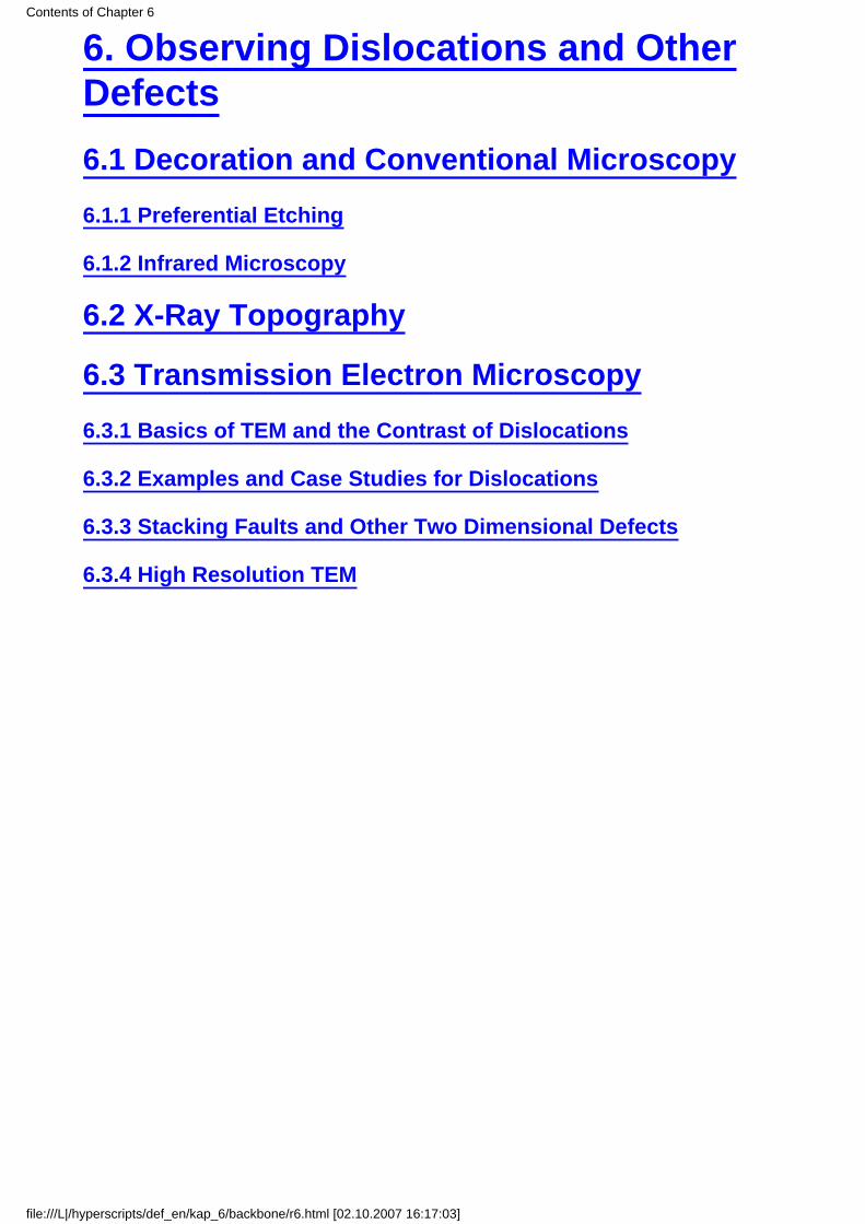
6. Observing Dislocations and OtherDefects
6.1 Decoration and Conventional Microscopy
6.1.1 Preferential Etching
6.1.2 Infrared Microscopy
6.2 X-Ray Topography
6.3 Transmission Electron Microscopy
6.3.1 Basics of TEM and the Contrast of Dislocations
6.3.2 Examples and Case Studies for Dislocations
6.3.3 Stacking Faults and Other Two Dimensional Defects
6.3.4 High Resolution TEM
Contents of Chapter 6
file:///L|/hyperscripts/def_en/kap_6/backbone/r6.html [02.10.2007 16:17:03]

6. Observing Dislocations and Other Defects
6.1 Decoration and Conventional Microscopy
6.1.1 Preferential Etching
Basics of Preferential Etching
The basic idea behind preferential etching is to mark defects intersecting the surface by a small pit or groove, so they become visible in amicroscope.
Start with a well polished surface that does not show any structures in a light microscope (including high magnifications and sensitive modes,e.g. phase or interference contrast
Find an etching solution that dissolves your material much more quickly around defects than in perfect regions (that is the tricky part).
Expose (= etch) your sample in this solution for an appropriate amount of time. What happens will be something like this:
Model crystal with several kinds of defects intersecting the (polished) surface on top,and surface structure after preferential etching of defects.
After preferential etching you obtain well developed etch pits (actually something looking more like pointed etch cones) at the intersection points ofdislocations (including partial dislocations) and the surface and etch grooves at the intersection line of grain boundaries and stacking faults with thesurface. Precipitates will be shown as shallow pits with varying size, depending on the size of the precipitate and its location in the removed surfacelayer. Areas with high densities of very small precipitates may just appear rough. Two-dimensional defects as grain boundaries and stacking faultsmay be delineated as grooves.
There is a certain problem with grain boundaries, however: They may also be delineated, i.e. rendered visible, with chemicals that do notpreferentially etch defects, but simply dissolve the material with a dissolution velocity that depends on the grain orientation (this is the rule andnot the exception for most chemicals).In this case grain boundaries show up as steps and not as grooves. Small steps and grooves, however, look very similar in a light microscope andmay easily be mixed up.
You may think: So what! - in any case I see the grain boundary. Well, almost right, but not quite - there are problems:
Grain boundaries separating two grains with similar orientation with respect to the surface would not be revealed.
The delineation of grain boundaries obtained under uncertain etching conditions suggests that you delineated all defects - but in fact you did not.Delineation of grain boundaries thus must not be taken as an indication that the etching procedure works and there are no defects, because youdon't see any!
Before we look at examples and case studies, two important points must be made:
1. Defect etching for many scientists is a paradigm for "black art" in science. There are good reasons for this view:
Nobody knows how to mix a preferential etching solution for some material from theoretical concepts. Of course you must look for chemicals ormixtures of chemicals that react with your material, but not too strongly. But after this bit of scientific advice you are on your own in trying tofind a suitable preferential etch for your material.Well-established preferential etching solutions usually have unknown and poorly understood properties. They sometimes work only on specificcrystallographic orientations; their detection limits for small precipitates are usually unknown; they may also depend on other parameters like thedoping level in semiconductors; and so on.
2. Defect etching in practice is more art then science.
Beginners, even under close supervision by a master of the art, will invariably produce etched samples with rich structures that have nothing to dowith defects - they produced so-called etch artifacts. It takes some practice to produce reliable results.But: Defect etching still is by far the most important and often most sensitive technique for observing and detecting defects!
There are many routine procedures for delineating the defects structure of metals by etching. Here we will focus on defects etching in Silicon; which isstill the major technique for defect investigations in Si technology. Some details and peculiarities of defect etching in Si can be found in the link. Inwhat follows we look at the power and possible mechanisms of preferential etching in the context of examples from recent research.
6.1.1 Observation of Dislocations and Other Defects
file:///L|/hyperscripts/def_en/kap_6/backbone/r6_1_1.html (1 of 4) [02.10.2007 16:17:04]

Defect Etching Applied to Swirl Defects in Silicon:
The name "Swirl defects" was used for grown-in defects in large Si crystals obtained by the float-zone technique in the seventies.
Swirl defects are a subspecies of what now is known as "bulk micro defects" (BMD); they are nothing but agglomerates of the point defectspresent in thermal equilibrium near the melting point with possible influences of supersaturated impurities still present in ultra clean Si (onlyoxygen and on occasion carbon).Whereas the relatively large swirl defects are no longer present in state-of-the-art Si crystals, point defect agglomerates and oxygen precipitatesstill are - there is no way to eliminate the equilibrium defects! BMDs are a major concern in the Si industry because they cause malfunctions ofintegrated circuits. The link leads to some recent papers on point defects and BMDs in Si crystals.
Most of the examples relating to Si are taken from the work of B.O. Kolbesen (formerly at Siemens; now(2001) at the University of Frankfurt).
The name "swirl" comes from the spiral "swirl-like" pattern observed in many cases by preferentialetching as shown on the right.
Close inspection revealed two types of etch features which must have been caused by different kindsof defects. Lacking any information about the precise nature of the defects (which etching can notgive), they were termed "A-" and "B-swirl defects". More pictures and information in the link
Understanding the precise nature of swirl defects was deemed to be very important for developing crystal growth techniques that could avoid thesedetrimental defects.
But etching alone can not give structural data, and other techniques as, e.g., transmission electron microscopy, could not be applied directlybecause the densities of swirl defects was too small (the likelihood of having a defect in a typical TEM sample was practically zero). Acombination of a special etching technique and TEM, however, could give the desired results.The power and the "black art" component of defect etching is nicely demonstrated by the following development: A "special etch" which wassimply the old solution, but cooled to about freezing temperatures, did not produce etch pits (and thus remove the defect) for A-swirls, buthillocks (still containing the defect).
The hillocks identified the precise location of the A-swirl defect. A special preparation technique rendered the areas containing hillocks transparent forTEM investigations, and the structure of A-swirls defects could be identified. They consisted of dislocation loop arrangements that were generated bythe agglomeration of interstitials. This gave the first direct evidence that self-interstitials are important in Si.
B-swirl defects could not be identified with this technique - their nature is still not clear.
More about swirl defects and the application of preferential etching can be found in an original paper (in German) in the link.
Process Control by Etching Defects during the Manufacture of Integrated Circuits
The manufacture of integrated circuits (IC) involves many processes prone to introduce defects in the more or less perfect starting crystal.
All high temperature processes induce temperature gradients which lead to stress and thus to a driving force for plastic deformation. Since thestarting material is dislocation free, the decisive process is the generation of the first dislocations which is much easier if small precipitates ordislocation lops are already present.Thermal oxidation introduces Si interstitials with a strong tendency to agglomerate into stacking fault loops, so-called oxidation inducedstacking faults (OSF).
All processes tend to induce trace amount of metals which will diffuse into the Si and eventually precipitate.
Ion implantation destroys the lattice to a large degree up to complete amorphization. Even upon careful annealing some defects may be left over.
As a general rule, all defects in the electronically active part of an IC (roughly the the first 5 µm - 10 µm of the wafer) are deadly for the device. Theyhave to be avoided and that means that they have to be monitored first. The method of choice is preferential etching.Lets look at an example
The pictures show a Si wafer with several defect types introduced during very early stages of processing. Details are provided in the link.
6.1.1 Observation of Dislocations and Other Defects
file:///L|/hyperscripts/def_en/kap_6/backbone/r6_1_1.html (2 of 4) [02.10.2007 16:17:04]
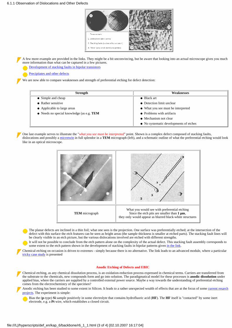
A few more example are provided in the links. They might be a bit unconvincing, but be aware that looking into an actual microscope gives you muchmore information than what can be captured in a few pictures.
Development of stacking faults in bipolar transistors
Precipitates and other defects
We are now able to compare weaknesses and strength of preferential etching for defect detection:
Strength Weaknesses
Simple and cheap●
Rather sensitive●
Applicable to large areas●
Needs no special knowledge (as e.g. TEM●
Black art●
Detection limit unclear●
What you see must be interpreted●
Problems with artifacts●
Mechanism not clear●
No systematic developments of etches●
One last example serves to illustrate the "what you see must be interpreted" point. Shown is a complex defect composed of stacking faults,dislocations and possibly a microtwin in full splendor in a TEM micrograph (left), and a schematic outline of what the preferential etching would looklike in an optical microscope.
TEM micrographWhat you would see with preferential etching
Since the etch pits are smaller than 1 µm,they only would appear as blurred black-white structures
The planar defects are inclined in a thin foil; what one sees is the projection. One surface was preferentially etched; at the intersection of thedefect with this surface the etch features can be seen as bright areas (the sample thickness is smaller at etched parts). The stacking fault lines willbe clearly visible in an etch picture, but the various dislocations involved are etched with different strengths.It will not be possible to conclude from the etch pattern alone on the complexity of the actual defect. This stacking fault assembly corresponds tosome extent to the etch pattern shown in the development of stacking faults in bipolar patterns given in the link.
Chemical etching on occasion is driven to extremes - simply because there is no alternative. The link leads to an advanced module, where a particulartricky case study is presented
Anodic Etching of Defects and EBIC
Chemical etching, as any chemical dissolution process, is an oxidation-reduction process expressed in chemical terms. Carriers are transferred fromthe substrate to the chemicals, new compounds form and go into solution. The paradigmatical model for these processes is anodic dissolution underapplied bias, where the carriers are supplied by a controlled external power source. Maybe a way towards the understanding of preferential etchingcomes from the electrochemistry of the specimen?Anodic etching has been studied to some extent in Silicon. It leads to a rather unexpected wealth of effects that are at the focus of some current resarchprojects. The experiment is simple:
Bias the (p-type) Si sample positively in some electrolyte that contains hydrofluoric acid (HF). The HF itself is "contacted" by some inertelectrode, e.g. a Pt wire, which establishes a closed circuit.
6.1.1 Observation of Dislocations and Other Defects
file:///L|/hyperscripts/def_en/kap_6/backbone/r6_1_1.html (3 of 4) [02.10.2007 16:17:04]

The Si-HF- junction behaves to some extent like a Schottky junction; current flow, however, is always accompanied by a chemical reaction. Thecurrent density first increases steeply with the applied bias, then reaches a maximum (called jPSL; PSL stands for "porous Si layer") and decreasesagain (that is when the analogy with a Schottky junction fails), goes through a second maximum (called jox) and finally starts to oscillate .
In the "forward" regime of the junction, the reaction is the dissolution of Si (in reverse condition it is H2 evolution).
If a polished specimen that was subjected to a current density considerably smaller than the first peak value is inspected after some etching time, itsdefect will be revealed in a way reminiscent of purely chemical etching. This can be understood (in parts) by considering current flow in terms ofdiffusion current and generation currents as introduced in basic pn- (or Schottky)-junction theory. The major ingredients for anodic etching are shownbelow.
Basic experimental set-up, current flowand chemical reaction
Measured I-V-characteristic and theoretical plot of ln I vs.V with diffusionand generation currents. Around a defect the generation current is larger than in perfectSi.
Preferential defect etching thus can be understood in terms of current flow: At small current densities the generation currents are larger than thediffusion current, the area around electronically active defects (i.e. defects that generate carriers) should be etched more deeply and etch pits shouldappear. At larger current densities the differential etch rate should disappear. The experiments support this view to some extent; the link contains someresults
General results of anodic etching
The consideration of the influence of defects on a Schottky junction suggests a different approach to the detection of electronically active defects:Measure the local leakage current or radiation induced current of a junction. This can be done by injecting current locally by an electron beam througha thin Schottky barrier while measuring the induced current. Electronically active defects will recombine more carriers than the defect-free regions, thecurrent will be locally reduced.
This method exists and is called "electron beam induced current" technique (EBIC) if a scanning electron microscope is used as the basicinstrument. If a scanned light beam is used, we have the "light beam induced current" technique or LBIC; the mainstay of solar celldevelopment with poly crystalline Si.The principle of EBIC is shown in the link.
If one compares anodic etching, chemical etching and EBIC, much can be learned about defects and the detection methods, but many questionsremain open. Some examples are given in the link
Anodic etching is still a virulent research issue within the context of the general electrochemistry of semiconductors.
6.1.1 Observation of Dislocations and Other Defects
file:///L|/hyperscripts/def_en/kap_6/backbone/r6_1_1.html (4 of 4) [02.10.2007 16:17:04]

6.1.2 Infrared Microscopy
Materials that are transparent to visible or - more important - infra red light (IR) may be investigated intransmission. This usually requires that the sample is optically polished on both sides. Especiallysemiconductors are transparent in IR light and IR microscopy is often used to investigate defects;particularly in III-V compounds. Defects may be rendered visible by:
Polarization microscopy. Elastic strain fields may rotate the polarization angle of polarized lightto some (small) degree. The strain fields around defects can thus be made visible; an example isshown in the link.Absorption contrast. Precipitates, for example, consist of some other material with differentoptical properties - it may not be transparent to IR light. In this case they would be directly visibleas dark spots.
If the primary defects are not precipitates but e.g. small dislocation loops resulting from vacancyagglomeration, they may be turned into a precipitate by a technique called defect decoration. This isusually done as follows:
Diffuse a fast moving element into the sample (e.g. Li or Cu for Si) at relatively high temperatures(however, without changing the primary defect configuration).Cool down sufficiently fast to nucleate the precipitation of the decorating element only at defects,but not so fast that not enough diffusion jumps are possible and you do not get any precipitation. Ifyou cool too slowly, homogeneous nucleation may produce precipitates everywhere and thetechnique is useless.The primary defects are now heavily decorated with impurity precipitates and visible in IRmicroscopy (or other techniques). However, the dimensions have been enlarged, the primary defectstructure may have changed, and you must keep in mind that you are now looking at a differentdefect from what you wanted to study in the first place!
Nevertheless, IR-microscopy with or without decoration, has made important contributions to the studyof defects in crystals. Its weaknesses and strengths can be summarized as follows.
Strength Weaknesses
Relatively cheap●
Partiallyquantitative(strain fields)
●
Large and smallareas can beinvestigated atmediumresolution (ca. 1µm).
●
Well polishedsurfaces on bothsides required
●
Involvedspecimenpreparation ifdecoration isused
●
Often not veryspecific as to thenature of defects
●
Only applicableto "medium"defect densities
●
Not overlysensitive
●
Interpretationuncertain ifdecorationtechniques areused.
●
© H. Föll
6.1.2 Infrared Microscopy
file:///L|/hyperscripts/def_en/kap_6/backbone/r6_1_2.html [02.10.2007 16:17:04]

6.2 X-Ray Topography
There are no efficient lenses for X-rays and therefore no X-ray microscopes. Still, there are ways toimage defects with X-rays.
The essential part for imaging defects in crystals is the diffraction of the X-rays in the crystallattice. This is in contrast to the conventional X-ray imaging technique in medical applications werethe differential absorption of X-rays in differently dense tissue is used.
The basic principle (which is also valid for imaging with electron beams in the transmission electronmicroscope) is shown below:
The specimen is oriented with respect to the incoming wave in such a way that theBragg-condition for diffraction is only met (or nearly met) for just one set of lattice planes.All defects with strain fields will locally deform the lattice and thus change the Bragg conditionlocally. The intensity of the diffracted beam will react to this and vary around defects. This isschematically shown below
In the example, the specimen is oriented in such a way thatthe Bragg condition in the perfect part of the crystal isalmost, but not quite met. There will be no diffraction or,more quantitatively speaking, a rather low intensity of thediffracted beam. The primary beam thus is transmittedalmost without any losses.
To the left-hand side of the edge dislocation, the strainfield bends the lattice plane locally into the Bragg position.In this area the primary beam is strongly diffracted andloses intensity.
The intensity of the diffracted beam is mirror symmetric tothe primary beam.
For the imaging of defects (typically in Si-wafers, with or without processing) the following basic set-upis used.
An X-ray source with a thin "one-dimensional" beam cross-section illuminates a line of the wafer. Onlythe primary beam (or, for dark-field imaging, the diffracted beam) is admitted through an aperture on thefilm. Wafer, aperture, and film are scanned through the beam.Some examples of X-ray topography are given in the following links; another one we have alreadyencountered before.
Total view and resolution limit
Case study in bipolar technique
6.2.1 X-Ray Topography
file:///L|/hyperscripts/def_en/kap_6/backbone/r6_2_1.html (1 of 2) [02.10.2007 16:17:04]

The strengths and weaknesses of X-ray topography are quite apparent:
Strength Weaknesses
Imaging oflarge waferswith goodresolution(ca. 5 µm)possible
●
Detailedanalysis(e.g.Burgersvectors)possiblewithinlimits
●
Nospecimenpreparationnecessary
●
Very expensive●
rather long exposuretimes even withpowerful (typically50 kW) X-ray tubes
●
Resolution/sensitivitynot good enough forsingle/small defects
●
6.2.1 X-Ray Topography
file:///L|/hyperscripts/def_en/kap_6/backbone/r6_2_1.html (2 of 2) [02.10.2007 16:17:04]

6.3 Transmission Electron Microscopy
6.3.1 Basics of TEM and the Contrast of Dislocations
Transmission electron microscopy (TEM) is by far the most important technique for studying defectsin great detail. Much of what was stated before about defects would be speculative theory, or wouldnever have been conceived without TEM.Using TEM, we look through a piece of material with electron "waves," usually at high magnification.
In contrast to X-ray imaging, lenses for electron beams exist: Magnetic fields (and, in principle,electric fields, too) can be made with gradients that act as convex lenses for the electron waves. Forvery general reasons it is not possible to construct electromagnetic concave lenses and that meansthat imaging systems are not very good because lens aberrations cannot be corrected as inconventional optics.Still, the intensity distribution of the electron waves leaving the specimen can be magnified by anelectron optical system and resolutions of ≈ 0,1 nm are attainable.The electrons interact with the material in two ways: inelastic and elastic scattering. Inelasticscattering (leading eventually to absorption) must be avoided since it contains no local information.The electron beam then will be only elastically scattered, i.e. diffracted; the lattice and the defectspresent modulate amplitude and phase of the primary beam and the diffracted beams locally.The energy of the monochromatic electron beam is somewhere between (100 - 400) keV, specialinstruments go up to 1,5 MeV (at a price of ca. 8 M€). Keeping inelastic scattering of the electronssmall has supremacy, this demands specimen thicknesses between 10 nm to ca. 1 µm. Theresolution depends on the thickness; high-resolution TEM (HRTEM) demands specimensthicknesses in the nm region.
This has a major consequence: The total volume of the material investigated by TEM since it started inthe fifties, is less than 1 cm3!
Taking and interpreting TEM images is a high art; it takes several years of practice. The major partof any TEM investigation is the specimen preparation. Obtaining specimens thin enough andcontaining the defects to be investigated in the right geometry (e.g. in cross-section) is a science initself.Still, practically all detailed information about extended defects comes from TEM investigationswhich do not only show the defects but, using proper theory, provide quantitative information aboute.g. strain fields.
The key is the electron-optical system. It not only serves to magnify the intensity (and, in HRTEM, thephase) distribution of the electron waves of the electron waves leaving the specimen, but, at the throw ofa switch, provides electron diffraction patterns. The picture shows the basic electron-optical design of aTEM
At least four (usually five) imaginglenses are needed in addition to twocondenser lenses (not shown). For mostimaging modes an aperture right afterthe objective lens must be provided.
The beam paths for the diffraction modeand the imaging mode are shown on theleft.
The most important lens is the objectivelens. Its resolution limit defines theresolution of the whole microscope.
6.3.1 Basics of TEM and the Contrast of Dislocations
file:///L|/hyperscripts/def_en/kap_6/backbone/r6_3_1.html (1 of 3) [02.10.2007 16:17:05]

The aperture after the objective lens isessential for the conventional imagingmodes. It is usually set to only admit theprimary beam, or one of the diffractedbeams into the optical system.
The image, or better, the contrast of a dislocation depends on several parameters. Most important are:
The diffraction conditions. Is the Bragg condition fulfilled for many reciprocal lattice vectors g,for none, or just for two? All cases are easily adjusted by tilting the specimen relative to theelectron beam while watching the diffraction pattern. The preferred condition for regular imaging isthe "two-beam" case with only one "reflex" excited; i.e. the Bragg condition is only met for onepoint in the reciprocal lattice or one diffraction vector g (usually with small Miller indices, e.g.{111} or {220}.The excitation error: Is the Bragg condition met exactly (excitation error = 0; dynamical case) oronly approximately (excitation error < 0 or > 0; kinematical case).The magnitude of the scalar product between the reciprocal lattice vector g and the Burgers vectorb, g · b. If it is zero or very small, the contrast is weak, i.e. the dislocation is invisible.The imaging mode. Is the primary beam admitted through the aperture and used for imaging(bright field condition), or a diffracted beam (dark field condition)? In other word, is it theintensity distribution of the primary beam or of a diffracted beam that constitutes the image? Or areseveral beams used whose interference produces a high-resolution image?
How is the proper diffraction condition selected experimentally? Fortunately, a little bit of inelasticscattering produces so-called Kikuchi lines which provide a precise and easily interpretable guide to theexact diffraction condition obtained by tilting the specimen. The link shows examples.
The following picture illustrates some imaging conditions for dislocations with maximum andminimum gb product.
We may draw the following conclusions; they are justified by the full theory of TEM contrast.
Dislocations are invisible or exhibit only weak contrast if g · b = 0. This can be used for a Burgersvector analysis by imaging the same dislocation with different diffraction vectors and observingthe contrast.Under kinematic bright field conditions (Bragg condition met almost, but not quite), the dislocationis imaged as a dark line on a bright background. The width of the line corresponds to the width ofthe region next to one side of the dislocation where the Bragg condition is now met; which isusually several nm.Under dark field conditions the dislocation appears bright on a dark background.
6.3.1 Basics of TEM and the Contrast of Dislocations
file:///L|/hyperscripts/def_en/kap_6/backbone/r6_3_1.html (2 of 3) [02.10.2007 16:17:05]
Under dark field conditions with large excitation errors the Bragg condition is only met in a smallregion close to the core of the dislocation. The image consists of a thin white line on a pitch blackbackground. This is the so-called "weak-beam" condition; it has the highest resolution ofconventional imaging modes. It is hard to use, however, because almost nothing is seen on thescreen (making adjustments difficult) and long exposure times are needed which are only practicalwith a very stable instrument.
6.3.1 Basics of TEM and the Contrast of Dislocations
file:///L|/hyperscripts/def_en/kap_6/backbone/r6_3_1.html (3 of 3) [02.10.2007 16:17:05]

6.3.2 Examples and Case Studies for Dislocations
In what follows a few examples for imaging dislocations with TEM are shown. Where possible,examples have been selected that have been used before (e.g. in the context of dislocation loopformations) or will be used later (e.g. in the context of defects in boundaries).The first example demonstrates the contrast of dislocations as a function of the excitation error
The specimen was bent a little; so the excitation error changes from left to right. On the left handside, the excitation error is relatively large; on the right hand side it is small. The contrast on the leftis weak, but the resolution is good; on the right hand side the dislocation appears a as strong, butblurred black line.
The second example demonstrates the contrast disappearance for g · b = 0.
Shown is a network of pure screw dislocations in Si which we will encounter again in the context ofgrain boundaries.
Only one set of dislocations shows up in the dark field conditions employed for the g = {220} typeof diffraction vector which is parallel to one Burgers vector and perpendicular to the other one.With a g = {400} diffraction vector both sets of dislocation are imaged, but there is a loss of clarity.
Next we will see how a dislocation loop can be analyzed.
Shown are dislocation loops of the "A-swirl defects" imaged with two different diffraction vectors(drawn in as arrows) and a +g/–g pair. In the first image, the contrast of the lower dislocation loophas disappeared (the fuzzy line is due to the precipitates along the dislocation line). The twopictures on the right show the lower loop, the image is wide or narrow, depending on the sign of thediffraction vector g.
6.3.2 Examples and Case Studies for Dislocations
file:///L|/hyperscripts/def_en/kap_6/backbone/r6_3_2.html (1 of 4) [02.10.2007 16:17:06]

This is an important effect because it allows to analyze the nature of a dislocation loop asschematically illustrated below. The image of the loop lies inside or outside the geometricprojection; upon reversing the sign of g or b (and this means switching from vacancy to interstitialtype), the image switches between the two extremes.
For a given geometry it is possible to predict if the contrast is "inside" or "outside"; the nature of aloop may thus be determined. But beware! There are many possibilities of committing a sign error!Printing the negative with emulsion side up or down, e.g., will exchange the signs and turn avacancy loop into an interstitial loop or vice versa.
The next example compares regular dark field and weak-beam conditions. The object is a very densedislocation network with a complicated structure which we will encounter again in the context of grainboundaries.
6.3.2 Examples and Case Studies for Dislocations
file:///L|/hyperscripts/def_en/kap_6/backbone/r6_3_2.html (2 of 4) [02.10.2007 16:17:06]

The weak-beam image on the left shows a lot more detail, but the signal to noise ratio is rather bad.This is about the limit of the resolution obtainable under weak beam conditions.In the link, a comparison between weak-beam conditions and bright field can be found.
The last picture shows conventional bright field imaging.
The tip of a probe produced some mechanical damage in the emitter area of a transistor in anintegrated circuit (the bright square area in the center of the tangle). A microcrack was generated(the elongated black shape); upon heating in the next processing cycle the dislocation tangle wasformed to relieve the stress.
6.3.2 Examples and Case Studies for Dislocations
file:///L|/hyperscripts/def_en/kap_6/backbone/r6_3_2.html (3 of 4) [02.10.2007 16:17:06]

By tilting the specimen while keeping the imaging conditions constant (this involves a rotationaround the diffraction vector), a second picture can be obtained under a somewhat different imagingdirection. The two pictures can be viewed in a stereo viewer and will produce the fullthree-dimensional glory of the structure.
More examples can be found in the links
Weak-beam image of a dislocation network involving partial dislocations under different diffractionconditionsUnknown ribbon defect in Si, showing difficulties in interpretationRadiation damage in Co showing possibilities of interpretationFeSi precipitates in SiPrismatic punching of dislocation loops from precipitatesHelix dislocations produced by climb of screw dislocationsDislocations in TiAl being pinned by debrisPtSi on Si showing the power of diffractions patterns (for another example use the link)Comparison weak beam - bright field
© H. Föll
6.3.2 Examples and Case Studies for Dislocations
file:///L|/hyperscripts/def_en/kap_6/backbone/r6_3_2.html (4 of 4) [02.10.2007 16:17:06]

6.3.3 Stacking Faults and Other Two Dimensional Defects
Stacking faults
Two-dimensional defects like stacking faults, but, to some extent also grain- and phase boundaries, giverise to some special contrast features.
Stacking faults are best seen and identified under dynamical two-beam condition; i.e. the Braggcondition is exactly met for one point in the reciprocal lattice.This automatically implies that the diffracted beam, if seen as the primary beam, also meets theBragg condition; it is diffracted back into the primary beam wave field.This leads to an oscillation of the intensity between the primary and the diffracted beam as afunction of depth in the sample; the "wave length" of this periodic intensity variations is called theextinction length ξ.
For a wedge-shaped specimen, the intensity of the primary or diffracted wave thus changes with thelocal thickness; it goes through maxima and minima.
The illustration shows the resulting image: a system of black and white fringes, called thicknessfringes or thickness contours is seen on the screen.On top a schematicdrawing, on the bottom thereal thing. In this case it is an etch pit in a Ge sample which is the usual inverted pyramid with{111} planes.
A stacking fault can be seen as the boundary between two wedge shaped crystals which are in directcontact, but with a displacement R along the wedge.
As a result, the two fringe systems resulting from the two wedges do not fit together anymore. Anew fringe system develops delineating the stacking fault; we see the typical stacking fault fringes
6.3.3 Stacking Faults and Other Defects
file:///L|/hyperscripts/def_en/kap_6/backbone/r6_3_3.html (1 of 3) [02.10.2007 16:17:07]

Again, getting all the signs right, the nature of the stacking fault can be determined. If intrinsicstacking faults under some imaging conditions would start with a white fringe, extrinsic stackingfaults would start with a black one. Reversing the sign of the diffraction vector g or thedisplacement vector R changes white to black and vice versa.
If more kinematical conditions are chosen, the amplitude of the intensity oscillation decreases; thestacking fault contrast assumes an average intensity that is usually different from the normal backgroundintensity - stacking faults appear in grey.
A few examples: The picture below shows three defects that behave as predicted and could be stackingfaults. Indeed, the small defect in the top half and the very large defect are stacking faults. The smallerdefect in the bottom part, however is a micro twin. This is not evident from one picture, but can beconcluded from contrast analysis.
The next picture shows a complicated arrangement of several stacking faults:
6.3.3 Stacking Faults and Other Defects
file:///L|/hyperscripts/def_en/kap_6/backbone/r6_3_3.html (2 of 3) [02.10.2007 16:17:07]

A whole system of overlapping oxidationinduced stacking faults in Si. Thebiggest loop was truncated by thespecimen preparation; the fringe systemwhere the stacking fault intersects withone surface is clearly visible.
The other surface was preferentiallyetched; the etch pits down the (Frank)dislocation lines are clearly visible.
The overlap of several stacking faultsleads to changing background contrasts -from black to no contrast (whenevermultiples of three stacking faults overlap)to almost white.
Similar if less complicated contrast effects were already encountered in illustrations given before inthe context of point defect agglomeration.More examples of a typical oxidation induced stacking faults in Si (OSF) are given in the link
But there are limits to TEM analysis: Sometimes defects are observed which resist analysis. Oneexample is shown in the link; another one we will encounter in the next subchapter.
Other Defects
The strain-induced contrast of dislocations due to local intensity variations in the primary and diffractedbeams and the fringe contrast of stacking faults due to local phase shifts of the electron waves, if takentogether, are sufficient to explain (quantitatively) the contrast of any defect.
It may get involved, and not everything seen in TEM micrographs will be easily explained, but ingeneral, contrast analysis is possible and the detailed structure of the defect seen can be revealedwithin the limits of the resolution (you cannot, e.g., find a kink in a dislocation (size ca. 0,3 nm)with a typical kinematical bright field resolution of 5 nm).
In the links a gallery of micrographs is provided with a wide spectrum of defects. Bear in mind that mostexamples are from single crystalline and relatively defect free Silicon. The images of regularpoly-crystalline materials would be totally dominated by their grain boundaries (see the examples at theend of the list).
Small dislocation loops in Cobalt produced by ion-implantation.
Precipitates in Silicon with dislocation structures.
Needle shaped FeSi2 precipitates in Si; the bane of early IC technology.
Helical dislocations resulting from the climb of screw dislocations.
Bowed-out dislocations in a TiAl alloy; kept in place by point defects and small precipitates.
A thin film of PtSi on Si as an example of the "real" world of fine-grained materials.
Overview of TiAl as an example of a specimen with a high defect density.
6.3.3 Stacking Faults and Other Defects
file:///L|/hyperscripts/def_en/kap_6/backbone/r6_3_3.html (3 of 3) [02.10.2007 16:17:07]

6.3.4 High Resolution TEM
High-Resolution TEM (HRTEM) is the ultimate tool in imaging defects. In favorable cases it showsdirectly a two-dimensional projection of the crystal with defects and all.
Of course, this only makes sense if the two-dimensional projection is down some low-indexdirection, so atoms are exactly on top of each other.
The basic principle of HRTEM is easy to grasp:
Consider a very thin slice of crystal that has been tilted so that a low-index direction is exactlyperpendicular to the electron beam. All lattice planes about parallel to the electron beam will beclose enough to the Bragg position and will diffract the primary beam.The diffraction pattern is the Fourier transform of the periodic potential for the electrons in twodimensions. In the objective lens all diffracted beams and the primary beam are brought togetheragain; their interference provides a back-transformation and leads to an enlarged picture of theperiodic potential.This picture is magnified by the following electron-optical system and finally seen on the screen atmagnifications of typically 106.
The practice of HRTEM, however, is more difficult them the simple theory. A first illustration serves tomake a few points:
The image shows one of the first HRTEM images taken around 1979; it is the <110> projection ofthe Si-lattice; a schematic drawing is provided for comparison. It also contains a few special grainboundaries, called twin boundaries.
We notice a few obvious features:
Instead of two atoms we only see a dark "blob."
Or does the dark blob signal the open channels in the lattice projection? There is actually no way oftelling from just one picture.The twin boundaries look fine in comparison to the drawing at a first glance. Looking more closely,one realizes that there are a few unclear points: The yellow arrow points to "fuzzy" lattice planes tothe right (or left) of the boundary. Following a fringe across the boundary seems to result in anoffset - what does it mean? But what should we expect defects (in this case the twin boundaries) tolook like? After all, they destroy the periodicity of the lattice and it is not obvious what Fouriertransforms of defects will produce in general cases.
The last point is easy to solve: Just do a simulation of a defect (i.e. calculate the image for an assumedslice of a crystal with all atoms at the proper positions), but mind the points mentioned below! These arethe limitations to HRTEM stemming from the non-ideality of the instrument and the specimen:
The specimen is not arbitrarily thin! If the thickness is in the order of the extinction length, somereflexes may have very small intensities because they were diffracted back into the primary beam.The objective lens then will not be able to reconstruct the spatial frequencies contained in thesereflections; the image looks like a different lattice.
6.3.4 High Resolution TEM
file:///L|/hyperscripts/def_en/kap_6/backbone/r6_3_4.html (1 of 4) [02.10.2007 16:17:09]
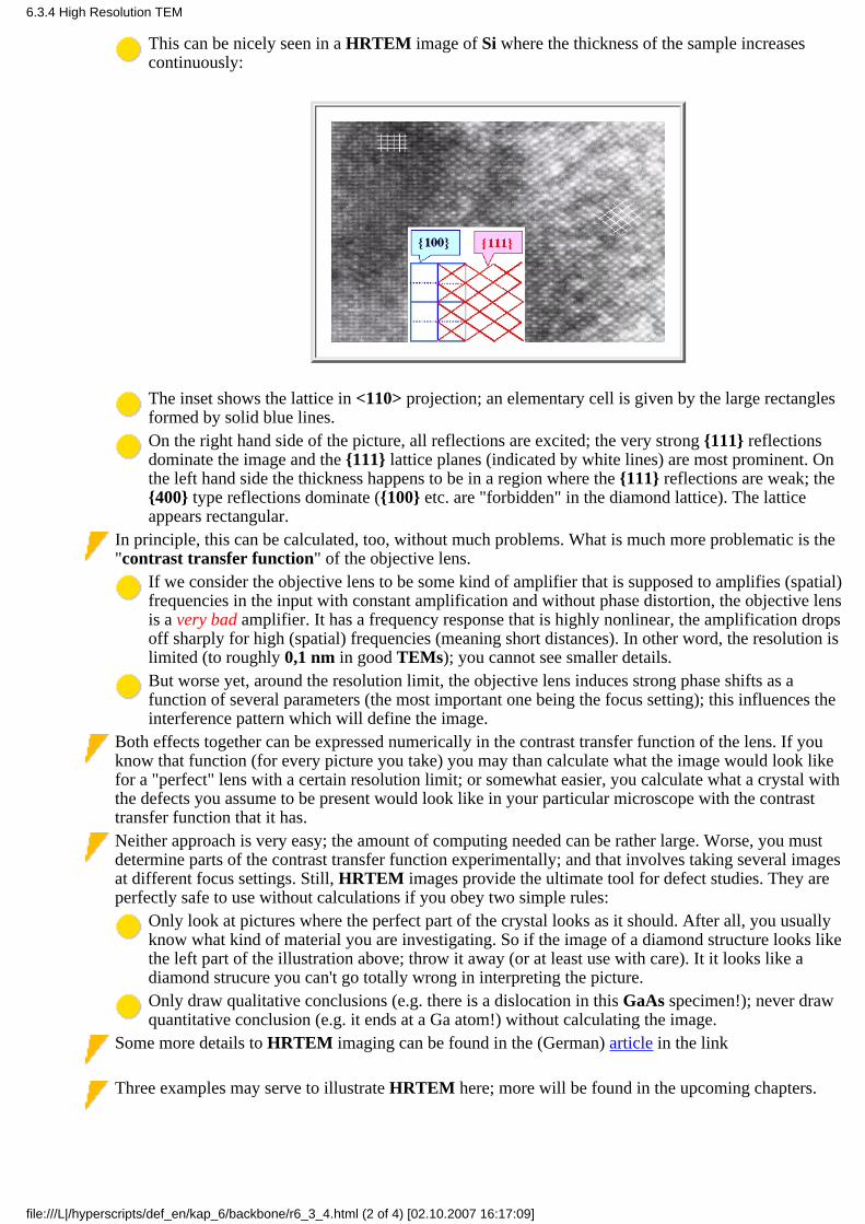
This can be nicely seen in a HRTEM image of Si where the thickness of the sample increasescontinuously:
The inset shows the lattice in <110> projection; an elementary cell is given by the large rectanglesformed by solid blue lines.On the right hand side of the picture, all reflections are excited; the very strong {111} reflectionsdominate the image and the {111} lattice planes (indicated by white lines) are most prominent. Onthe left hand side the thickness happens to be in a region where the {111} reflections are weak; the{400} type reflections dominate ({100} etc. are "forbidden" in the diamond lattice). The latticeappears rectangular.
In principle, this can be calculated, too, without much problems. What is much more problematic is the"contrast transfer function" of the objective lens.
If we consider the objective lens to be some kind of amplifier that is supposed to amplifies (spatial)frequencies in the input with constant amplification and without phase distortion, the objective lensis a very bad amplifier. It has a frequency response that is highly nonlinear, the amplification dropsoff sharply for high (spatial) frequencies (meaning short distances). In other word, the resolution islimited (to roughly 0,1 nm in good TEMs); you cannot see smaller details.But worse yet, around the resolution limit, the objective lens induces strong phase shifts as afunction of several parameters (the most important one being the focus setting); this influences theinterference pattern which will define the image.
Both effects together can be expressed numerically in the contrast transfer function of the lens. If youknow that function (for every picture you take) you may than calculate what the image would look likefor a "perfect" lens with a certain resolution limit; or somewhat easier, you calculate what a crystal withthe defects you assume to be present would look like in your particular microscope with the contrasttransfer function that it has.Neither approach is very easy; the amount of computing needed can be rather large. Worse, you mustdetermine parts of the contrast transfer function experimentally; and that involves taking several imagesat different focus settings. Still, HRTEM images provide the ultimate tool for defect studies. They areperfectly safe to use without calculations if you obey two simple rules:
Only look at pictures where the perfect part of the crystal looks as it should. After all, you usuallyknow what kind of material you are investigating. So if the image of a diamond structure looks likethe left part of the illustration above; throw it away (or at least use with care). It it looks like adiamond strucure you can't go totally wrong in interpreting the picture.Only draw qualitative conclusions (e.g. there is a dislocation in this GaAs specimen!); never drawquantitative conclusion (e.g. it ends at a Ga atom!) without calculating the image.
Some more details to HRTEM imaging can be found in the (German) article in the link
Three examples may serve to illustrate HRTEM here; more will be found in the upcoming chapters.
6.3.4 High Resolution TEM
file:///L|/hyperscripts/def_en/kap_6/backbone/r6_3_4.html (2 of 4) [02.10.2007 16:17:09]

The first picture shows a small angle grain boundary in Si. This was the first picture of this kind; itonly can be interpreted qualitatively; the contrast transfer function was not known. What we seebeyond doubt are several lined-up dislocations which constitute a boundary - the top half of thelattice is tilted with respect to the bottom half.
The next picture (from W. Bergholz) shows an SiO2 precipitate in Si. Again, a qualitativeinterpretation is neither possible nor necessary. It is clear that the precipitate, albeit very small, isnot spherical
Courtesy of W. Bergholz
The last example shows quantitative HRTEM (from W. Jäger) Careful imaging under variousconditions, extraction of the contrast transfer function and prodigious computing allowed not onlyto image a sequence of Si - Ge multilayers produced by molecular beam epitaxy (MBE), but toidentify the positions of the Si and Ge atoms. The first picture shows an overview. The brighterregions indicate the Ge layers, but it is not clear exactly how the lattice changes from Si to Ge.
6.3.4 High Resolution TEM
file:///L|/hyperscripts/def_en/kap_6/backbone/r6_3_4.html (3 of 4) [02.10.2007 16:17:09]

Courtesy of W. Jäger
This image also demonstrates the progress made in building electron microscopes. The "old"pictures shown above were taken with a the best general-purpose TEM available around 1980(Siemens Elmiskop 102). The last pictures were taken with a TEM optimized for high resolutionaround 1995.
Next a comparison between an enlarged part of the Ge/Si stack is shown together with a quantitativeevaluation of this and other pictures obtained at different focus settings from W. Jaeger and his group.The color codes defined Ge concentrations and a very clear representation of the multilayer sequence isobtained.
Courtesy of W. Jäger
6.3.4 High Resolution TEM
file:///L|/hyperscripts/def_en/kap_6/backbone/r6_3_4.html (4 of 4) [02.10.2007 16:17:09]

7. Grain Boundaries
7.1 Coincidence Lattices
7.1.1 Twin Boundaries
7.1.2 The Coincidence Site Lattice
7.1.3 The DSC Lattice and Defects in Grain Boundaries:
7.2 Grain Boundary Dislocations
7.2.1 Small Angle Grain Boundaries and Beyond
7.2.2 Case Studies: Small Angle Grain Boundaries in Silicon I
7.2.3 Case Studies: Small Angle Grain Boundaries in Silicon II
7.2.4 Generalization
7.3 O-Lattice Theory
7.3.1 The Basic Concept
7.3.2 Working with the O-Lattice
7.3.3 The Significance of the O-Lattice
7.3.4 Periodic O-Lattices and Pattern Elements
7.3.5 Pattern Shift and DSC Lattice
7.3.6 Large Angle Grain Boundaries and Final Points
Contents of Chapter 7
file:///L|/hyperscripts/def_en/kap_7/backbone/r7.html [02.10.2007 16:17:09]

7. Grain Boundaries
7.1 Coincidence Lattices
7.1.1 Twin Boundaries
General Remarks
So-called "twin boundaries" are the most frequently encountered grain boundaries in Silicon, but alsoin many other fcc crystals. This must be correlated to an especially low value of the interface energy orgrain boundary energy always associated with a grain boundary. This becomes immediatelyunderstandable if we construct a (coherent) twin boundary. The qualifier "coherent" is needed at thispoint, we will learn about its meaning below.
Lets look at the familiar <110> projection of the diamond lattice:
Now we introduce a stacking fault, e.g. by adding the next layer in mirror-symmetry (structuralchemists would call this a "cis" instead of a "trans" relation):
If we were to continue in the old stacking sequence, we would have produced a stacking fault.However, if we continue with mirror-symmetric layers, we obtain the following structure withoutchanging any bond lengths or bond angles:
7.1.1 Grain Boundaries
file:///L|/hyperscripts/def_en/kap_7/backbone/r7_1_1.html (1 of 6) [02.10.2007 16:17:09]

We generated a (coherent) twin boundary! This is obviously a special grain boundary with a highdegree of symmetry.
Now let's try to describe what we did in general geometric terms. To describe the twin boundary fromabove or just any boundary geometrically, we look at the general case illustrated below:
We have two arbitrarily oriented grains joinedtogether at the boundary plane. We thus need todefine the "arbitrary" orientation and separatelythe boundary plane.
Choosing grain I as reference, we now can always"produce" a arbitrary orientation of the second grainby "cutting" a part of grain I off - along theboundary plane - and then rotating it by arbitraryangles α, β and γ around the x-, y- and z- axis(always defined in the reference crystal, here grainI).
Of course, the grain II thus produced would notfit together anymore with grain I. So we simplyremove or add grain II material, until a fit isproduced.Alternatively, we could simply rotate thesecond crystal around one angle α if we pick asuitable polar vector for that.
Specifying this polar (unit) vector will need twonumbers or its direction - e.g. two anglesrelative to the boundary plane or any otherreference plane, and one number for its lengthspecifying the angle of rotation.In either way: three numbers then for theorientation part.
The boundary then is defined by 5 parameters: The three rotation angles needed to "produce" grain II,and two parameters to define the boundary plane by its Miller indices {hkl} in the coordinate system ofthe reference grain I.
Why do we need only two parameters to define the boundary plane? After all, we usually needthree Miller indices {hkl} to indicate a plane in a crystal?
7.1.1 Grain Boundaries
file:///L|/hyperscripts/def_en/kap_7/backbone/r7_1_1.html (2 of 6) [02.10.2007 16:17:09]

Good question! We need only two numbers in this case because here a unit vector with the rightorientation given by {hkl} is sufficient - the length, likewise encoded in {hkl}, does not matter.Since you need only two angles between a unit vector and the coordinate axis' to describe itunambiguously, two numbers are enough, even so they cannot be given straightforward in {hkl}terms.The third angle is then always given by the Euler relation
sin2α + sin2β + sin2γ = 1
Again, Miller indices do not only give the direction of a vector perpendicular to a crystallographicplane, but also a specified length which contains the distance between the indexed crystallographicplanes - and that's why they need three numbers in contrast to a unit vector.
Thus, constructing a simple (coherent) twin boundary, looking at it and generalizing somewhat, welearned a simple truth:
A (simple) grain boundary needs (at least)5 parameters
for its geometric description
That was some basic geometry for a simple grain boundary! For real grain boundaries we must add thecomplications that may prevail, e.g.:
The grain boundary is not flat (not on one plane), but arbitrarily bent.
The grain boundary contains (atomic) steps and other local "grain boundary defects".
The grain boundary contains foreign atoms or even precipitates.
The grain boundary is not crystalline but consists of a thin amorphous layer between the grains.
Since all those (and more) complications are actually observed, we must (albeit reluctantly) conclude:
Grain boundaries are rather complicated defects!
Detailed Consideration of the Coherent Twin Boundary
We can learn more about grain boundaries by analyzing our (coherent) twin somewhat more. While wegenerated this defect by adding {111} layers in a mirror-symmetric way, there are other ways of doing it,too:We first consider the twin boundary as a pure twist boundary. The recipe for creating a twist boundaryfollowing the general recipe from above is as follows:
Cut the crystal along a {111} plane (using Volterras knife, of course).
Rotate the upper part by 180° or 60° around an axis perpendicular to the cut plane (= "twist")
Weld the two crystals together. There will be no problem, everything fits and all bonds findpartners.
7.1.1 Grain Boundaries
file:///L|/hyperscripts/def_en/kap_7/backbone/r7_1_1.html (3 of 6) [02.10.2007 16:17:09]

This procedure is shown below. We are forced to conclude that we obtain exactly the same twinboundary that we produced above!
Now lets look at the other extreme: We construct our twin boundary as a pure tilt boundary. The recipefor creating a tilt boundary following the general recipe from above is as follows:
Cut the crystal along a {111} plane (using Volterras knife, of course)
Rotate the upper part by 70.53° around an axis perpendicular to the drawing plane (= "tilt" thegrain); i.e. use a <110> direction for rotating.Now, however, we must fill in or remove material as necessary.
Weld together.
This procedure is shown above; again we obtain exactly the same twin boundary we had before!
This is not overly surprising, after all the symmetries of the crystal should be found in theconstruction of grain boundaries, too. Well this is conceptually easy to grasp, it generates a major problem in the mathematical analysis ofthe grain boundary structure. What you want to do then is to generate a grain boundary by somecoordinate transformation of one grain, and than analyze its properties with respect to the necessarytransformation matrix. If there are several (usually infinitely many) possible matrices, all producingthe same final result, you have a problem in picking the "right" one. We will run into that problemin chapter 7.3.
Grain Boundary Orientation and Energy
Now lets look at the energy of the twin boundary and see if we can generalize the findings. We areinterested in answering the following questions:
Is the grain boundary energy (= the energy needed to generate 1 cm2 of grain boundary) a functionof the 5 parameters needed to describe the boundary? The answer, of course, will be yes, so now weask:
7.1.1 Grain Boundaries
file:///L|/hyperscripts/def_en/kap_7/backbone/r7_1_1.html (4 of 6) [02.10.2007 16:17:09]

For a given orientation, could a small change in the three angles describing that orientation inducelarge changes in the energy? Asking a bit more pointedly: Are there orientations leading toboundaries with especially small or large energies? Are there favorable and unfavorableorientations?For a given orientation, are there possibilities to minimize the energy, e.g. by changing theboundary plane? Are there favorable and unfavorable planes?
We will be able to answer these question to some extent by using our twin boundary. First lets look atthe energy of the (coherent) twin boundary as shown above.
We would expect a rather small energy per unit area, because we did not have to change bondlengths or angles. We should expect that the energy of a (coherent) twin boundary should becomparable to that of a stacking fault.
It is hard to imagine a boundary with lower energy and this explains why one always finds a lot oftwin boundaries in cubic (and hexagonally) close-packed crystals
Now lets generate a twin boundary with the "twist" or "tilt" recipe, but with twist or tilt angles slightlyoff the proper values. Lets assume a twist angle of e.g. 58° instead of 60°. We then make a boundarywith a similar, but distinctly different orientation.
Try it! Can't be done. Nothing will fit any more; a lot of bonds must be stretched or shortened andbent to make them fit. No doubt, the energy will increase dramatically. In other words:
The energy of a grain boundary may dependent very much on the precise orientation relationship
Next lets imagine the generation of a twin boundary where the twist or tilt angle is exactly right, butwhere the cut-plane is slightly off {111}. The result looks like the schematic drawing below:
Again, we have a hard time with the welding procedure. Some atoms will find partners with a slightadjustment of bonds, but other are in awkward positions, e.g. the atoms colored blue in the aboveillustration. The energy will be much higher than for a {111} plane - for sure. In other words:
The energy of a grain boundary may dependent very much on the Miller Indices of its plane
We now can understand the meaning of the qualifier "coherent" in connection with a twinboundary: Only twin boundaries on {111} planes are simple boundaries; they are called coherent todistinguish them from the many possible incoherent twin boundaries with planes other than {111}.
Optimization of Grain Boundary Energies
From the last observation we can easily deduce a first recipe for optimizing, i.e. lowering, the energy ofa given grain boundary:
Decompose the grain boundary plane into planes with low energies. If that cannot be done, form atleast large areas on low-energy planes and small areas of connecting high-energy planes. In otherwords, approximate the plane by a zig-zag configuration of planes.This process is called facet forming or facetting, the boundary plane forms facets. This isillustrated below.
7.1.1 Grain Boundaries
file:///L|/hyperscripts/def_en/kap_7/backbone/r7_1_1.html (5 of 6) [02.10.2007 16:17:09]

Grain boundary on low-energy plane (i.e. a{111} plane for a twin boundary). The {111}planes are indicated by the dashed lines
Grain boundary on high -energy plane
Energy optimization by facetting on {111}.The total area increases somewhat, but theenergy decreases.
This is an important insight with far-reaching consequences: We need no longer worry very much aboutthe grain boundary plane! It is always possible to optimize the energy by facetting.
Facetting involves, of course, the movement of atoms. However, only small movements ormovements over small distances are needed, so facetting is not too difficult if the temperatures arenot too low. So the crystal has an option - it can change the boundary plane by moving a few atomsaround.Experience, too, seem to show that boundary planes are not very important: Grain boundaries, asrevealed by etching or other methods, are usually rather curved and do not seem to "favor"particular planes - with the exception of coherent twins. This, however, is simply an illusionbecause the facetting takes place on such a small scale that it is not visible at optical resolution.
We now must deal with the relation between the relative orientation and the grain boundary energy.Two questions come to mind:
Are there any other low-energy orientations besides the rotations around <111> or <110> thatproduces the low-energy twin boundary?Is there a way to minimize the energy of a grain boundary that is close to, but not exactly in a lowenergy orientation (some analogon to the facetting of the planes)?This is not an easy question, because the crystal does not have an option of changing theorientation relationsship. In principle it would be possible, but it would imply moving a lot ofatoms - all the atoms inside a grain - and that is rather unlikely to occur.
Answering these questions will lead us to an important theory for the structure of grain boundaries (andphase boundaries) which will be the subject of the next sub-chapter.
7.1.1 Grain Boundaries
file:///L|/hyperscripts/def_en/kap_7/backbone/r7_1_1.html (6 of 6) [02.10.2007 16:17:09]

7.1.2 The Coincidence Site Lattice
If we look at the infinity of possible orientations of two grains relative to each other, we will find somespecial orientations. In two dimensions this is easy to see if we rotate two lattices on top of each other.
You can watch what will happen for a hexagonal lattice lattice by activating the link.
A so-called Moirée pattern develops, and for certain angles some lattice points of lattice 1 coincideexactly with some lattice points of lattice 2. A kind of superstructure, a coincidence site lattice (CSL),develops. A question comes to mind: Do these special coincidence orientations and the related CSLhave any significance for grain boundaries?Lets look at our paragon of grain boundaries, the twin boundary:
Shown are the two grains of the preceding twinboundary, but superimposed. Coinciding atoms(in the projection) are marked red. However, thismight be coincidental (excuse the pun), becausethe atoms in this drawing are not all in thedrawing plane. Note that it is not relevant if theboundary itself is coherent or not - only theorientation of the grains counts.And once more, note that the lattice is not thecrystal! We are looking for coinciding latticepoints - not for coinciding atom positions (butthis may be almost the same thing with simplecrystals). So in this picture the same situation is shown forthe fcc lattice belonging to the grain boundary.Again, coinciding lattice points are marked redand a (two-dimensional) elementary cell of theCSL is also shown in red. The two(three-dimensional) elementary cells of the fcclattices are also indicated.It is definite from this picture that the the twinboundary belongs to the class of boundaries witha coincidence relation between the two latticesinvolved.
From the animation in the link above it was clear that many coincidence relations exist for two identicaltwo-dimensional lattices. In order to be able to extend the CSL consideration to three dimensions and togeneralize it, we have to classify the various possibilities. We do that by the following definition:
Definition:The relation between the number of lattice points in the unit cell of
a CSL and the number of lattice points in a unit cell of thegenerating lattice is called Σ (Sigma); it is the unit cell volume ofthe CSL in units of the unit cell volume of the elementary cells of
the crystals.
A given Σ specifies the relation between the two grains unambiguously - although this is not easy tosee for, let's say, two orthorhombic or even triclinic lattices.
7.1.2 The Coincidence Site Lattice
file:///L|/hyperscripts/def_en/kap_7/backbone/r7_1_2.html (1 of 4) [02.10.2007 16:17:10]

If we look at the twin boundary situation above, we see that Σtwin = 3 (you must relate thetwo-dimensional lattices her; one is pointed above out in black!). For the three-dimensional case we stillobtain Σ = 3 for the twin boundary, so we will call twin boundaries from now on: Σ3 boundaries.
A Σ1 boundary thus would denote a perfect (or nearly perfect) crystal; i.e. no boundary at all.However. boundaries relatively close to the Σ1 orientation are all boundaries with only smallmisorientations called "small-angle grain boundaries" - and they will be subsumed under the termΣ1 boundaries for reason explained shortly.
Since the numerical value of Σ is always odd, the twin boundary is the grain boundary with themost special coincidence orientation there is, i.e. with the largest number of coinciding latticepoints.
Next in line would be the Σ5 relation defining the Σ5 boundary. It is (for the two-dimensional case) mosteasily seen by rotating two square lattices on top of each other.
This also looks like a pretty "fitting" kind of boundary, i.e. a low energy configuration.
A suspicion arises: Could it be that grain boundaries between grains in a CSL orientation, especially ifthe Σ values are low, have particularly small grain boundary energies?The answer is: Yes, but... . And the "but" includes several problems:
Most important: How do we get an answer? Calculating grain boundary energies is still very hard todo from first principles (Remember, that we can't calculate melting points either, even though its allin the bonds). First principles means that you get the exact positions of the atoms (i.e. the atomicstructure of the boundary and the energy). Even if you guess at the positions (which looks prettyeasy for a coherent twin boundary, but your guess would still be wrong in many cases because ofso-called "rigid body translations"), it is hard to calculate reliable energies.
So we are left with experiments. This involves other problems:
How do you measure grain boundary energies?
How do you get the orientation relationship?
How do you account for the part of the energy that comes from the habit plane of the boundary -after all, a coherent twin (habit plane = {111}) has a much smaller energy than an incoherent one?
Getting experimental results appears to be rather difficult or at least rather time consuming - and so it is!
Nevertheless, results have been obtained and, yes, low Σ boundaries tend to have lower energiesthan average.
However, the energy does not correlate in an easy way with Σ; it does not e.g. increasemonotonously with increasing Σ. There might be some Σ values with especially low energy values,whereas others are not very special if compared to a random orientation.
The result of (simple) calculations for special cubic geometries are shown in the picture:
7.1.2 The Coincidence Site Lattice
file:///L|/hyperscripts/def_en/kap_7/backbone/r7_1_2.html (2 of 4) [02.10.2007 16:17:10]

Shown is the calculated (0oK) energy for symmetric tilt boundaries in Al produced by rotatingaround a <100> axis (left) or a <110> axis (right). We see that the energies are lower, indeed, inlow Σ orientations, but that it is hard to assign precise numbers or trends. Identical Σ values withdifferent energies correspond to identical grain orientation relationships, but different habit planesof the grain boundary.
The next figure shows grain boundary energies for twist boundaries in Cu that were actually measuredby Miura et al. in 1990 (with an elegant and ingenious, but still quite tedious method).
Clearly, some Σ boundaries have low energies, but not necessarily all.
Nevertheless, in practice, you tend to find low Σ boundaries, because (probably) all low energy grainboundaries are boundaries with a defined Σ value. And these boundaries may have special properties indifferent contexts, too.
The link shows the critical current density (at which the superconducting state will be destroyed) inthe high-temperature superconductor YBa2Cu3O7 with intentionally introduced grain boundaries ofvarious orientations and HRTEM image of one (facetted) boundary. It is clearly seen that thecritical current density has a pronounced maxima which corresponds to a low Σ orientation in this(Perovskite type) lattice.
However, despite this or other direct evidence for the special role of low Σ boundaries, the most clearindication that low Σ boundaries are preferred comes from innumerable observations of a differentnature altogether - the observation that grain boundaries very often contain secondary defects with aspecific role: They correct for small deviations from a special low Σ orientation.
In other words: Low Σ orientations must be preferred, because otherwise the crystal would not"spend" some energy to create defects to compensate for deviations.
7.1.2 The Coincidence Site Lattice
file:///L|/hyperscripts/def_en/kap_7/backbone/r7_1_2.html (3 of 4) [02.10.2007 16:17:10]

If we accept that rule, we also have an immediate rule for preferred habit planes of the boundary:
Obviously, the best match can be made if as many CSL points as possible are contained in theplane of the boundary. This simply means:Preferred grain boundary planes are the closest packed planes of the corresponding CSL lattice.
We will look at those grain boundary defects in the next sub-chapter.
7.1.2 The Coincidence Site Lattice
file:///L|/hyperscripts/def_en/kap_7/backbone/r7_1_2.html (4 of 4) [02.10.2007 16:17:10]

7.1.3 The DSC Lattice and Defects in Grain Boundaries:
Grain boundaries may contain special defects that only exist in grain boundaries; the most prominentones are grain boundary dislocations. Grain boundary dislocations are linear defects with all thecharacteristics of lattice dislocations, but with very specific Burgers vectors that can only occur in grainboundaries.
To construct grain boundary dislocations, we can use the universal Volterra definition.We start witha "low Σ" boundary and make a cut in the habit plane of the boundary. The cut line, as before, willdefine the dislocation line vector l which by definition will be contained in the boundary.Now we displace one grain with respect to the other grain by the Burgers vector b so as to preservethe structure of the boundary everywhere except around the dislocation line. In other words: thestructure of the boundary after the shift looks exactly as before the shift.
What does that mean? What is the "structure of the boundary" and how do we preserve it?
Well, we have a CSL on both sides of the boundary. We certainly will preserve the structure of theboundary if we shift by a translation vector of the CSL, i.e. by a rather large Burgers vector. Wethan would preserve the coincidence site lattice - which is fine, but far too limited. We alreadypreserve the structure of the boundary if we simply preserve the coincidence!It is best to illustrate what this means with a simple animation: Two superimposed lattices form aCSL marked in blue. The red lattice moves to the left, and at first there are no more coincidences oflattice points - the CSL has disappeared and we have a different structure. However, after a shortdistance of shifting - far smaller than a lattice vector of the CSL, coincidence points appears and wehave a CSL again - but with the coincidence points now in different positions.
We found a displacement vector that preserved the structure of the boundary - sort ofexperimentally. There are others, too, and the possible displacements vectors that conserve the CSLobviously are not limited to vectors of the crystal lattice; they can be much smaller. This we cangeneralize:
The set of all possible displacement vectors which preserve the CSL defines a new kind of lattice, theso-called DSC-lattice. The abbreviation "DSC" stands for "Displacement Shift Complete", not the bestof possible names, but time-honored by now.
A better way of thinking about it would be to interprete the abbreviation as "Displacements whichare Symmetry Conserving". Displacing one grain of a grain boundary with a CSL by a vector of thecorresponding DSC lattice thus preserves the structure of the boundary because it preserves thesymmetries of the CSL. We now conclude:Translation vectors of the DSC lattice are possible Burgers vectors bGB for grain boundarydislocations. As for lattice dislocations, only the smallest possible values will be encountered forenergetic reasons.Grain boundary dislocations constructed in this way by (Volterra) definition, have most of theproperties of real dislocations - just with the added restriction that they are confined to theboundary. Strain- and stress field, line energy, interactions, forming of networks - everythingfollows the same equations and rules that we found for lattice dislocations.
7.1.3 The DSC Lattice and Defects in Grain Boundaries:
file:///L|/hyperscripts/def_en/kap_7/backbone/r7_1_3.html (1 of 3) [02.10.2007 16:17:10]

It remains to be seen how the DSC-lattice can be constructed. From the illustration it is clear thatevery vector that moves a lattice site of grain 1 to a lattice site of grain 2 is a DSC-lattice vector.This leads to a simple "working" definition:
The DSC-lattice is the coarsest sub-lattice of the CSL that has all atoms of both lattices on its latticepoints. Most lattice points of the DSC-lattice, however, will be empty
This is the DSC-lattice for the animation above. Itseasy enough to obtain, but:
A formal and general definition of the DSC lattice(including near CSL orientations) is one of the mostdifficult undertakings in grain boundary theory. Ifyou love tough nuts, turn to chapter 7.3 and proceed.
Any translation of one of the two crystals along a vector of the orange DSC-lattice will keep theCSL, but will generally shift its origin. Only if a DSC vector is chosen that is also a vector of theCSL, will the origin of the CSL remain in place.
Looking back at the Σ5 boundary from before, we now can enact the cut and the displacementprocedure and generate a picture of the dislocations that must result. The result contains a littlesurprise and is shown in cross-section below:
The cut was made from the right. The top crystal (red lattice points) was shifted by a unit vector ofthe DSC lattice, which is a 1/5<210> vector in both crystal lattices in this case. The second crystal(green lattice points) was left completely unchanged. The coincidence points are blue. We observetwo somewhat surprising effects:The boundary plane (as indicate by the pink line) after the shift is not identical with the plane of thecut
7.1.3 The DSC Lattice and Defects in Grain Boundaries:
file:///L|/hyperscripts/def_en/kap_7/backbone/r7_1_3.html (2 of 3) [02.10.2007 16:17:10]

The CSL has an interruption in both grains - it doesn't fit anymore. Disturbing - but totallyunimportant. The CSL, after all, is totally meaningless for real crystals - the (mathematical)coincidence points in the grains have no significance for the grains. The only significance of acoincidence orientation is that it provides an especially good fit of the two grains at a boundary, i.e.it allows for a particularly favorable boundary structure. And the structure of the grain boundary isunchanged by the introduction of the grain boundary dislocation, except around its core region.This is indicated by the characteristic diamond shapes (yellow) in the picture above that can betaken as the hallmark of this Σ5 structure.Think about it! Finding the yellow diamonds is the practical way of finding the position of theboundary. However you define the position - you will find the preserved structure as expressed inthe yellow diamonds here.Introducing the grain boundary dislocation thus had the unexpected additional effect of introducinga step in the grain boundary. Some atoms had to be changed from green to red to obtain thestructure, but that again is an artifact of the representation. Real atoms are all the same; they do notcome in green and red and do not care to which crystal they belong.
We see that the recipe works: Dislocations in the DSC lattice preserve the structure of the boundary;they leave the coincidence relation unchanged. However, they also may introduce steps in the plane ofthe boundary -we cannot yet be sure that this always the case.
Note that is not directly obvious how the step relates to the dislocation, i.e. how the vectordescribing the step can be deduced from the DSC lattice vector used as Burgers vector. (If you seean obvious relationship - please tell me. I'm not aware of a simple formula applicable in all cases).Note also: While many (if not all) grain boundary dislocations are linked with a step, the reverse isnot true: There are many possible steps in a boundary that do not have any dislocation character.More to that in chapter 8.3
The extension to three dimensions is obvious, but also a bit mind-boggling. Still, some general rules canbe given
The larger the elementary cell of the CSL, the smaller the elementary cell of the DSC-lattice!
If you suspected it by now: The DSC lattice indeed can be seen as the reciprocal lattice (in space)of the CSL.
The volumes of CSL, crystal lattice and DSC lattice relate as Σ : 1 : Σ –1 for cubic crystals.
What are all these lattices good for? The main import is:
A grain boundary between two grains that is close to, but not exactly at a low-energy (= low Σ)orientation may decrease its energy if grain boundary dislocations with a Burgers vector of the DSClattice belonging to the low-Σ orientation are introduced so that the dislocation free parts are now inthe precise CSL orientation and all the misalignment is taken up by the grain boundarydislocations. We will see how this works in the next sub-chapter.
7.1.3 The DSC Lattice and Defects in Grain Boundaries:
file:///L|/hyperscripts/def_en/kap_7/backbone/r7_1_3.html (3 of 3) [02.10.2007 16:17:10]

7.2 Grain Boundary Dislocations
7.2.1 Small Angle Grain Boundaries and Beyond
The determination of the precise dislocation structure needed to transform a near-coincidence boundaryinto a true coincidence boundary with some superimposed grain boundary dislocation network can beexceedingly difficult (to you, not to the crystal), especially when the steps possibly associated with thegrain boundary dislocations must be accounted for, too.
Nevertheless, the structure thus obtained is what you will see in a TEM picture - the crystal has noproblem whatsoever to "solve" this problem!
In order to get familiar with the concept, it is easiest, to consider the environment of the Σ= 1 grainboundary, i.e. the boundary between two crystals with almost identical orientation.
This kind of boundary is known as "small-angle grain boundary" (SAGB) , or, as already usedabove as "Σ1 boundary".We can easily imagine the two extreme cases: A pure tilt and a pure twist boundary; they are shownbelow.
Obviously, we are somewhat off the Σ1 position. Introducing grain boundary dislocations now willestablish the exact Σ1 relation between the dislocations (and something heavily disturbed at thedislocation cores). The DSC-lattice as well the CSL are identical with the crystal lattice in thiscase, so the grain-boundary dislocations are simple lattice dislocations.Introducing a sequence of edge dislocations in the tilt case and a network (not necessarily square)of screw dislocations in the twist case will do the necessary transformation; this is schematicallyshown below
7.2.1 Small Angle Grain Boundaries and Beyond
file:///L|/hyperscripts/def_en/kap_7/backbone/r7_2_1.html (1 of 5) [02.10.2007 16:17:11]

This may not be directly obvious, but we will be looking at those structures in great detail in the nextparagraph. Here we note the important points again:
Between the dislocation lines we now have a perfect Σ1 relation (apart from some elastic bending).
All of the misfit relative to a perfect Σ orientation is concentrated in the grain boundarydislocations.We thus lowered the grain boundary energy in the area between the dislocations and raised it alongthe dislocations - there is the possibility of optimizing the grain boundary energy. The outcomequite generally is:
Grain boundaries containing grain boundary dislocations which account for small misfits relative to apreferred (low) Σ orientation, are in general preferable to dislocation-free boundaries.
The Burgers vectors of the grain boundary dislocations could be translation vectors of one of thecrystals, but that is energetically not favorable because the Burgers vectors are large and the energyof a dislocation scales with Gb2 and there is a much better alternative:
The dislocations accounting for small deviations from a low Σ orientation are dislocations in theDSC lattice belonging to the CSL lattice that the grain boundary Σ endeavors to assume. Whyshould that be so? There are several reasons:
Dislocations in the DSC lattice belong to both crystals since the DSC lattice is defined inboth crystals.
1.
Burgers vectors of the DSC lattice are smaller than Burgers vectors of the crystal lattice, theenergy of several DSC lattice dislocations with a Burgers vector sum equal to that of acrystal lattice dislocations thus is always much smaller. WithΣibi(DSC) = b(Lattice), we always haveΣibi
2(DSC) << b2(Lattice).This is exactly the same consideration as in the case of lattice dislocations split into partialdislocations.
2.
A dislocation arrangement with the same "Burgers vector count" along some arbitraryvector r produces exactly the same displacement (remember the basic Volterra definitionand the double cut procedure).
3.
In other words: We can always imagine a low angle boundary of crystal lattice dislocations thatproduces exactly the small misorientation needed to turn an arbitrary boundary to the nearest low Σposition and superimpose it on this boundary.
Next, we decompose the crystal lattice dislocations into dislocations of the DSC lattice belongingto the low Σ orientation.This will be the dislocation network that we are going to find in the real boundary!
Lets illustrate this. First we construct another kind of DSC lattice dislocation, very similar, but differentto the one we had before. The coincidence points are marked in blue, atoms of the two crystal lattices ingreen and red.
7.2.1 Small Angle Grain Boundaries and Beyond
file:///L|/hyperscripts/def_en/kap_7/backbone/r7_2_1.html (2 of 5) [02.10.2007 16:17:11]

The plane of the cut now is perpendicular to the boundary and extends, by necessity, all the way tothe boundary. We produced a DSC edge dislocation with a Burgers vector perpendicular to theboundary plane (and a step of the boundary plane).
If we were to repeat this procedure at regular intervals along the boundary, we obtain the structureschematically outlined below.
In essence, we superimposed a tilt component with a tilt angle α that for small angles is given by isgiven by
α = d
b
with d = spacing of the DSC lattice dislocations and b = Burgers vector of the DSC latticedislocations.
In short, we can do everything with DSC lattice dislocations in a grain boundary that we can do withcrystal lattice dislocations. This leads to the crucial question alluded to before:
How do we calculate the DSC-lattice? As an example for the most general case of grain boundariesin triclinic lattices? Or even worse: For phase boundaries between two different lattices (withdifferent lattice constants)?
The answer is: Use the "Bollmann theory or "O-lattice theory" - it covers (almost) everything.
7.2.1 Small Angle Grain Boundaries and Beyond
file:///L|/hyperscripts/def_en/kap_7/backbone/r7_2_1.html (3 of 5) [02.10.2007 16:17:11]

However, unless you are willing to devote a few months of your time in learning the concept andthe math of the O-lattice theory, you will encounter problems - it is not an easy concept to grasp.We will deal with the O-lattice theory in a backbone II section, here we note that the mostimportant cases have been tabulated. Some solutions for fcc crystals are given in the table:
Σ Generation b from DSC-lattice
1 "Small-angle GB" a/2 <110>, possibly split into partials
3 Twin a/6 <112>, a/3 <111>
5 37° around <100> a/10 <130>
9 39,9° around <110> 1/18<114>, 1/9<122>, 1/18<127>,
19 26,5° around <110> a/38 <116>, a/19<133>, a/19 <10,9,3>
41 12,7° around <100> a/82<41,5,4>, a/82<910>, ...
Interestingly (and very satisfyingly), the DSC lattice vectors belonging to the Σ = 3 boundary areour old acquaintances, the partial Burgers vectors associated with stacking faults in the crystallattice.
This is but natural - a Σ = 3 twin boundary is after all a very close relative to stacking faults.
Now a question might come up: Σ = 41 is not exactly a "low Σ" value; and Burgers vectors ofa/82<41,5,4> appear to be a bit odd, too. So does this still make sense? Are boundaries close to a Σ41orientation still special and bound to have grain boundary dislocations?
Only the experiment can tell. The following TEM picture shows a Σ41 grain boundary (fromDingley and Pond, Acta Met. 27, 667, 1979)
A network of grain boundary dislocations withBurgers vectors b = a/82 <41,5,4> and anaverage distance of 20 nm is visible. The twosets of dislocations run parallel to the linesindicated by H and J.
Sorry, but it is there, even at Σ = 41. Why - wedo not really know, although Bollmann theorydoes provide an answer on occasion.
Obviously, if you want to understand the structure of grain boundaries, you must accept the concept ofgrain boundary dislocations even at rather large values of Σ and correspondingly low values of theBurgers vectors.
7.2.1 Small Angle Grain Boundaries and Beyond
file:///L|/hyperscripts/def_en/kap_7/backbone/r7_2_1.html (4 of 5) [02.10.2007 16:17:11]

In the next paragraph we will study some cases in more detail.
7.2.1 Small Angle Grain Boundaries and Beyond
file:///L|/hyperscripts/def_en/kap_7/backbone/r7_2_1.html (5 of 5) [02.10.2007 16:17:11]

7.2.2 Case Studies: Small Angle Grain Boundaries in Silicon I
First we will take a close look at some small angle grain boundaries in Silicon. Whereas they are the most simpleboundaries imaginable, they are still complex enough to merit some attention. They are also suitable to demonstrate a fewmore essential properties of grain boundary dislocations.
Lets first look at a pure tilt boundary as outlined in the preceding paragraph. Below is shown how edge dislocationscan accommodate the misfit relative to the Σ = 1 orientation (for a boundary plane that contains the dislocationslines).
The distance d between the dislocations is for small tilt angles α asbefore given by
α = d
b
This is a simple version of a general relation betwen Burgers vectors andmisorientation in small angle grain boundaries called Franks formula(more correctly Frank-Bilby formula).
In real life it looks slightly more complicated - but not much:
This is an early HRTEM of a small angle tilt boundary in Si. The redlines mark the edge dislocations, the blue lines indicate the tilt angle.
This picture nicely illustrates that we have indeed a Σ1 relationship inthe area between the dislocations, i.e. a perfect crystal. The dislocationsare not all in a row, but that does not really matter.
Next, we look at twist boundaries.
These and some of the other boundaries were artificially produced to study the structure. Two specimens of Si with adesired orientation relationship were placed on top of each other and "sintered" or "welded" together at hightemperatures. This process, first called "sintering" is now known as "waferbonding" and used for technicalapplications.The result for a slight twist between {100} planes is shown in the next picture:
7.2.2 Case Studies: Small Angle Grain Boundaries in Silicon I
file:///L|/hyperscripts/def_en/kap_7/backbone/r7_2_2.html (1 of 4) [02.10.2007 16:17:11]
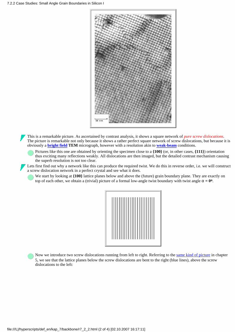
This is a remarkable picture. As ascertained by contrast analysis, it shows a square network of pure screw dislocations.The picture is remarkable not only because it shows a rather perfect square network of screw dislocations, but because it isobviously a bright field TEM micrograph, however with a resolution akin to weak-beam conditions.
Pictures like this one are obtained by orienting the specimen close to a {100} (or, in other cases, {111}) orientationthus exciting many reflections weakly. All dislocations are then imaged, but the detailed contrast mechanism causingthe superb resolution is not too clear.
Lets first find out why a network like this can produce the required twist. We do this in reverse order, i.e. we will constructa screw dislocation network in a perfect crystal and see what it does.
We start by looking at {100} lattice planes below and above the (future) grain boundary plane. They are exactly ontop of each other, we obtain a (trivial) picture of a formal low-angle twist boundary with twist angle α = 0o.
Now we introduce two screw dislocations running from left to right. Referring to the same kind of picture in chapter5, we see that the lattice planes below the screw dislocations are bent to the right (blue lines), above the screwdislocations to the left:
7.2.2 Case Studies: Small Angle Grain Boundaries in Silicon I
file:///L|/hyperscripts/def_en/kap_7/backbone/r7_2_2.html (2 of 4) [02.10.2007 16:17:11]

With many dislocations, the average orientation of the lattice planes below the small angle grain boundary will rotateto the right, above to the left. The combined effect is shown below.
If we want to rotate not just one set of lattice planes, but all of the top part of the crystal, we need at least a second set ofscrew dislocations. This produces a screw dislocation network of the kind shown in the TEM micrograph above.
The relation between the twist angle α and the dislocation spacing d is again a simple version of the general casegiven in Franks formula:
α = b
d
A detailed drawing of this dislocation network structure can be viewed in the link.
With luck, it is possible to image the lattice plane in a HRTEM micrograph. The link shows examples - the onlyHRTEM image of screw dislocations obtained so far.
The exact geometry of the network for the same twist angle α in an arbitrary twist boundary depends on many factors:
The twist angle α which determines the spacing between the dislocations. For Σ = 1 boundaries it simply the twistangle itself, for arbitrary boundaries it is the twist angle needed to bring the boundary to the closest low Σ orientationThe Burgers vectors of the dislocations. Even in small-angle grain boundaries they could be perfect, or split intopartials. In arbitrary boundaries they must be grain boundary dislocations with a Burgers vector of the proper DSClattice. Note that a network of grain boundary screw dislocations simply superimposes some twist to whateverorientation the boundary has without those dislocations.The type of the dislocations. For an arbitrary twist plane, the Burgers vectors of the possible dislocations are notnecessarily contained in the grain boundary plane; the required pure screw dislocations do not exist. In this casemixed dislocations must be used with a component of the Burgers vector in the grain boundary plane.The symmetries of the two crystal planes in contact at the grain boundary - even low-angle twist boundaries with atwist around the <100> axis can be joined on planes other than {100}.The complications that may arise because the (perfect) dislocations split into partials. Obviously, that has nothappened in the case shown above. The reason most likely is that the splitting would have to be on two different{111} planes inclined to the boundary plane (look at your Thompson tetrahedron!) which leads to very unfavorableknot configurations. Since the distance between dislocations is of the same order of magnitude as the typical distancebetween partials, we do not observe splitting into partials or dissociation of the knots.
7.2.2 Case Studies: Small Angle Grain Boundaries in Silicon I
file:///L|/hyperscripts/def_en/kap_7/backbone/r7_2_2.html (3 of 4) [02.10.2007 16:17:11]

We now can understand the very regular square network shown in the picture above - it is really about the most simplestructure imaginable.
But we still need to explain the interruptions in the network; the lines along which the net is shifted. In fact, to see avery regular network like this you must be pretty lucky; more often than not often (artificially) made twist grainboundaries look like this:
Both pictures show the result of the attempt to make a pure twist boundary. Whereas the left one still looks like thepicture above - just with more interruption of the network - the right one does not convey the impression of a squarenetwork at all.The answer is that these grain boundaries must accommodate more that just a pure twist: There is also a tiltcomponent and the plane of the grain boundary is not exactly {100}. We will pick up this subject again in the nextparagraph; more information about the right-hand side picture can be found in the link.
7.2.2 Case Studies: Small Angle Grain Boundaries in Silicon I
file:///L|/hyperscripts/def_en/kap_7/backbone/r7_2_2.html (4 of 4) [02.10.2007 16:17:11]

7.2.3 Case Studies: Small Angle Grain Boundaries in Silicon II
The recipe for "making" small angle grain boundaries in Silicon given in the preceding paragraph can beused for twist boundaries on any plane, besides the {100} plane the {111} planes are particularinteresting.
The structure will be much more complicated and serves to illustrate the importance of the grainboundary plane for given orientations. The picture below is a bright-field TEM micrograph(obtained under the specific bright-field conditions that rival weak-beam resolution mentionedbefore) and shows all dislocations present.
This is also an example of what mayhappen to you when you sit down at anelectron microscope with your specimenand start to look at it.
You know what to expect (a small angletwist grain boundary) in general, but nowyou see fascinating things - can youunderstand what you see?
And, in extrapolation, can you understandwhat you see if you do not knowbeforehand what to expect?
Well, we can understand most of the structure seen above. Lets construct it step by step
There must be a network of screwdislocations with b = a/2<110>. Sincethree Burgers vectors of this kind arecontained in a given {111} plane, weexpect a hexagonal network as shownon the left.
The knots where six dislocations meetcan not be expected to be stable; wewould expect a splitting leading to thehoneycomb pattern illustrated on theleft (with a changed scale for clarity).
7.2.3 Case Studies: Small Angle Grain Boundaries in Silicon II
file:///L|/hyperscripts/def_en/kap_7/backbone/r7_2_3.html (1 of 3) [02.10.2007 16:17:12]

In contrast to the {100} twistboundary, the dislocations now cansplit into partial dislocations in theplane of the boundary, we expect thatthe dislocations are split in this case.Working through the geometry we seethat everything fits at one knot, it caneasily be extended in the way shown.This optimizes the energy gain bylarge separations between the partialswhile at the same time keeping thestacking fault area small.The "constricted" knots now look"funny" - again 6 dislocations meet atone point. Can we split the knot tosomething more favorable?
Indeed, we can, as shown on the left.However, we only can do this byintroducing more Shockleydislocations and extrinsic stackingfaults
Putting everything together we obtaina network of Shockley dislocationsthat corresponds exactly to what wesee in the regular parts of themicrograph above. The exactgeometry, of course, depends mainlyon the stacking fault energies - herewe may find differences if we wouldlook at similar grain boundaries inother fcc materials.
It remains to explain the various non-regularities of the picture.
Most conspicuous are the large "blobs" with just a trace of some hexagonal structure. They aresimply SiO2 precipitates left over from the welding process; the hexagonal structures are Moiréepatterns that always appear whenever two regular structures are put on top of each other.
The other irregularities are formed by a superposition of:
A few edge dislocations to accommodate some tilt component.
Dislocations that moved from somewhere in the crystal into the grain boundary where they werecaught and incorporated into the network. These dislocations are called extraneous or extrinsicgrain boundary dislocations because they are not an integral part of the grain boundary structure.Dislocations needed to accommodate steps, i.e. changes of the grain boundary plane measuring afew atomic distances.
7.2.3 Case Studies: Small Angle Grain Boundaries in Silicon II
file:///L|/hyperscripts/def_en/kap_7/backbone/r7_2_3.html (2 of 3) [02.10.2007 16:17:12]

It is not always clear or easily analyzed exactly what it is that you see. Especially the connectionbetween steps and intrinsic or extrinsic dislocation is, in general, quite complicated, because on the oneside most, but not all grain boundary dislocations automatically introduce steps, while on the other sidemost, but not all steps introduce dislocations. We will deal with that matter in more detail when dealingwith phase boundaries.
But we are not yet done with the low-angle twist boundary on {111}. The micrograph above shows onlypart of the structure. The micrograph below shows more:
The lower inset shows a magnified viewof the network from the lower half ofthe boundary; the upper inset from theupper half. (Click on the picture for anenlargement and more information),
Whereas the lower part shows thenetwork discussed above, the upper partshows something new: A rather simplenetwork with reduced spacing. Detailedanalysis reveals that the dislocations inthe upper part have Burgers vectors b =a/6<112>, but they are not properShockley partials, because there are nostacking faults between the dislocations.
They are rather dislocations in the DSClattice of a Σ = 3 boundary - in otherwords, the low angle twist boundary hassplit into two twin boundaries with asuperimposed dislocation network inone of the twin boundaries.
We may ask: Why? And in which twinboundary are the dislocations? Why arethey not in the perfect lattice betweenthe boundaries?
It seems to ever end. But in order not to have too much detail in the main backbone part, thesecomplications will be discussed in an advanced section.
7.2.3 Case Studies: Small Angle Grain Boundaries in Silicon II
file:///L|/hyperscripts/def_en/kap_7/backbone/r7_2_3.html (3 of 3) [02.10.2007 16:17:12]

7.2.4 Generalization
The relation between the spacing of the dislocations and the tilt- or twist angle in the special cases givenwas simple enough - but what about arbitrary small angle grain boundaries with twist and tiltcomponents? What kind of dislocation structure and what geometry should be expected?
As we have seen, the detailed structure of the network can be quite complicated and depends onmaterials parameters like stacking fault energies. We can not expect to have a simple formulagiving us the answers.The relation giving the distance between dislocations in a boundary and the orientation relationshipfor arbitrary low-angle orientations (meaning that the two rotation angles needed for a generaldescription are both small, lets say ≤ 10o - 15o) was first given by Frank. It is Franks formulareferred to before.
Franks formula is derived in the advanced section, here we only give the result. The low-angle grainboundary shall be described by:
Its dislocation network consisting of dislocations with Burgers vectors b.
An arbitrary vector r contained in the plane of the boundary.
A (small) angle α around an arbitrary axis described by the (unit) vector l (then one angle isenough) that describes the orientation relationship between the grains. We may then represent therotation by a polar vector R = α · l
Franks formula then is:
B = ( r × l ) · 2sinα
2
with B = sum of all the specific Burgers vectors bi cut by r ; i.e. B = Σi bi.
Since the formula is formally applicable to any boundary, but does not make much sense for largeangles α (can you see why?) we only consider low-angle boundaries. Then we can replace sin α/2approximately by α/2 and obtain the simplified version
B = ( r × l ) · α
Let's illustrate this:
7.2.4 Generalization
file:///L|/hyperscripts/def_en/kap_7/backbone/r7_2_4.html (1 of 2) [02.10.2007 16:17:12]

Shown are two vectors r1 and r2 contained in a boundary plane with an arbitrarily chosendislocation network consisting of two types of dislocations having Burgers vectors b1 and b2.
Franks formula ascertains that (r × l) · α equals the sum of the Burgers vectors encountered by r,i.e. B = 2b2 + 3b1 for r1, and B = 3b1 for r1 in the picture above.
This is a major achievement, but not overly helpful when you try to find out the geometry of thenetwork for some arbitrary boundary, because their is no simple and unique way of decomposing asum of Burgers vectors into its individual parts.
This "simple" formula, however, contains the special cases that we have considered before, and leavesenough room for complications. It does not, however, say anything about preferred planes or networkgeometries. For this one needs the full power of Bollmanns O-lattice theory.
Franks formula is not applicable to large angle grain boundaries because the distance between thedislocations would become so small as to be meaningless.
In this case the grain boundary may be viewed as the (dislocation free) "low Σ" boundary closest tothe actual orientation with a superimposed low-angle grain boundary formed by dislocations in thecorresponding DSC lattice.Franks formula then can be used for the low angle part and will give the correct over-all Burgersvector count.
The precise geometry of the network, however, can become hopelessly complicated because all theadditional features, e.g. extrinsic dislocations and steps, are not only still present but become morecomplicated, too.
In addition, some special perversions may evolve, e.g. the splitting of DSC lattice dislocations intopartial dislocations in the DSC lattice, producing stacking faults in the DSC lattice!And we are implicitly talking grain boundaries between cubic crystals! In less symmetric crystalseverything is even more complicated - it is time then to study O-lattice theory!
One last feature should be mentioned that now can be understood: The reactions of lattice dislocationsthat move into grain boundaries. So far, a grain boundary was just seen as an internal surface on which adislocation can somehow end.
Now we know better: It simply decomposes into the intrinsic (DSC-lattice) grain boundarydislocations present. This is quite satisfying because the logical problems encountered whenthinking more in more detail about how a dislocation "just ends" on a grain boundary. It is alsowhat one sees if looking closely, an example is shown in the illustration.
7.2.4 Generalization
file:///L|/hyperscripts/def_en/kap_7/backbone/r7_2_4.html (2 of 2) [02.10.2007 16:17:12]

7.3 O-Lattice Theory
7.3.1 The Basic Concept
Formulas here have plenty of indices, underlining etc. - and we will now give up the cursive font normally usedfor variables because it gets too cumbersome.
Basic Idea The Coincidence Site lattice (CSL) provided a relatively easy way to grasp the concept of special orientationsbetween grains that give cause for special grain boundaries. With the extension to grain boundary dislocations inthe DSC lattice, the CSL concept became in principle applicable to all grain boundaries, because any arbitraryorientation is "near" a CSL orientation. But yet, the CSL concept is not powerful enough to allow the deductionof grain boundary structures in all possible cases. The reasons for this are physical, practical and mathematical:
The CSL by itself is meaningless; meaningful is the special grain boundary structure that is possible if thereis a coincidence orientation. The grain boundary structure is special, because it is periodic (with theperiodicity of the CSL) and contains coincidence points (cf. the picture).
But we have no guarantee that periodic grain boundary structures may not exist in cases where no CSLexists; i.e. by only looking at CSL orientation, we may miss other special orientations. That will be certainlytrue whenever we consider boundaries between different lattices - be it that lattice constants of the samematerials changed ever so slightly because one grain has a somewhat different impurity concentration, orthat we look at phase boundaries between different crystals. If the lattice constants are incommensurable,there will be no CSL at all.
As we have seen, even a CSL with Σ = 41 is significant, even so it is virtually unrecognizable as anythingspecial in a drawing. This is an expression of the mathematical condition, that you either have perfectcoincidence or none. If two points coincide almost, but not quite, no recognizable CSL will be seen. If twolattice points coincide except for, lets say, 0,01 nm, we certainly would say we have a physical coincidence,but mathematically we have none.The same is true if we rotate a lattice away from a coincidence position by arbitrarily small angles.Mathematically, the coincidence is totally destroyed and the situation has completely changed, whereasphysically an arbitrarily small change of the orientation would be expected to cause only small changes inproperties.Only a very small fraction of grain orientations have a CSL. The "trick" we used to transform anyorientation into a coincidence orientation by introducing grain boundary dislocations in the DSC lattice issomewhat questionable: the effect (= CSL) comes before the cause (= dislocations in the DSC lattice),because at the orientation that we want to change no CSL and therefore no DSC lattice exists.
It becomes clear that the main problem lies in the discreteness of the CSL. Any useful theory for special grainboundary (and phase boundary) structures must be a continuum theory, i.e. give results for continuous variationsof the crystal orientation (and lattice type).
This theory exists, it is the so-called "O-lattice theory" of W. Bollmann; comprehensively published in hisopus magnus "Crystal Defects and Crystalline Interfaces" in 1970.
The O-lattice theory is not particularly easy to grasp. (Sorry, but it took me many hours, too). It is wellbeyond the scope of this hyperscript to go into details. What will be given is the basic concept, the big ideas;together with some formulas and a few examples. You should first read just over it, trying to get the basicideas, than study it point by point. If you don't get it the first time - don't despair, you are in good if notexcellent company!
There are two basic ideas behind the O-lattice theory:
1. Take a crystal lattice I and transform it in any way you like. That means you can not only rotate it into anarbitrary orientation relative to crystal I, but also deform it by stretching, squeezing and shearing it. Thecrystal lattice II generated in this way from a simple cubic lattice I thus could even be an arbitrarily orientedtriclinic lattice.2. Now look for coincidence points between lattice I and lattice II. But do not restrict the search forcoinciding lattice points, but expand the concept of coincidence to all "equivalence points" within twooverlapping unit cells. What equivalence points are becomes clear in the illustration.
7.3.1 The Basic Concept
file:///L|/hyperscripts/def_en/kap_7/backbone/r7_3_1.html (1 of 7) [02.10.2007 16:17:13]

Points in lattice I and lattice II are called equivalent, if their space vectors are identical (always in theirrespective lattice coordinate system).
The Basic Formula
Let's look at the example illustrated above. Lattice I is deformed by first rotating it and then stretching the axisx1; this produces lattice II
An arbitrary point within the elementary cell of lattice I is described by a vector r(I)
r(I) transforms into a vector r(II) by the transformation applied. The point reached within the unit cell oflattice II by r(II) is then an equivalence point to the one in crystal I.
Of course there is more than one equivalence point; there is always an infinite set defined by one point plus allpoints reachable by a lattice translation vector T from this particular point.
Any point r'(II) in lattice II belonging to the set as defined above can be described in the coordinate systemof lattice II (defined by the units vectors x1(II) and x2(II)) by
r'(II) = r(II) + T(II)
With T(II) = any translation vector of lattice II, or
T(II) = n · x1(II) + m · x2(II)
And n, m = 0, ± 1, ± 2, ...
All these points are by definition equivalence points to the corresponding set of points in lattice I given by
r'(I) = r(I) + T(I)
Let us designate the set of all equivalence points defined above in lattice I by C1 and the corresponding set inlattice II by C2 and, for the sake of clarity, all vectors pointing to equivalence points of the respective sets byr(C1) and r(C2).
If we now look at a certain equivalence point in lattice II, it always originated from lattice I by the generaltransformation as shown in the picture below
7.3.1 The Basic Concept
file:///L|/hyperscripts/def_en/kap_7/backbone/r7_3_1.html (2 of 7) [02.10.2007 16:17:13]

The blue lattice was obtained from the pink one by some transformation; in this case by a simple rotation.
The dark point with the red vector pointing to it is an arbitrary point in lattice I (for the sake of easyrecognition about in the center of a lattice I cell).After the transformation, it is now the red point at the apex of the blue and pink arrows in lattice II. It is stillabout in the center of a cell in lattice II, but for the particular transformation shown, it is now also about inthe center of a lattice I cell - there is (about) a coincidence of equivalence points.Let's assume perfect coincidence, then the red point denotes coinciding equivalence points, i.e. equivalencepoints that are "on top of each other".
We need a precise mathematical formulation that gives us the conditions under which coincidence of equivalencepoints occcurs.
This is easy, we just have to consider that for coinciding equivalence points the blue vector in lattice II canbe obtained in two ways:
By the transformation equation from the corresponding red vector of lattice I (valid for allequivalence points) or, since the coincidence point belongs to both lattices at once, by
1.
adding some translation vector of lattice I to the red vector. This is symbolically shown in the picture.2. In formulas we can write for any vector in lattice II pointing to some equivalent point of the set C2:
r(C2) = A {r(C1)}
r(C1) = A–1 {r(C2)}
With A = transformation matrix (we will encounter examples for A later; see also the basic module formatrix calculus) since this simply describes how lattice II originates from lattice I. This was the first waymentioned above.On the other hand, we can obtain new equivalence points in lattice I, i.e. other elements of the set C1designated by e(C1) quite generally by the equation
e(C1) = r(C1) + T(I)
We will now use these relations for coinciding equivalence points:
We are looking for coincidences of any one member of the set r(C1) with any one member of the set r(C2); anycoincidence point thus obtained will be named r0. Since this point, describable in lattice II by r(C2) must bereachable in lattice I by first going down r(C1) and then adding a translation vector of lattice I, we obtain
r(C2) = r(C1) + T(I) = r0
7.3.1 The Basic Concept
file:///L|/hyperscripts/def_en/kap_7/backbone/r7_3_1.html (3 of 7) [02.10.2007 16:17:13]

Using the transformation equation for lattice I from above and substituting it into the above equation yields
r0 = A–1 {r0} + T(I)
We wrote r0 instead of r(C2) because we do not need the distinction between the sets C1 and C2 any morebecause r0 belongs to both sets.
Rearranging the terms following matrix calculus by using the identity or unit transformation matrix I, weobtain the fundamental equation of O-lattice theory:
( I – A–1 ) r0 = T(I)
What does that equation mean?
For a given transformation, i.e. for given orientation relationship between two grains, its solution for r0defines all the coincidence points or O-points of the lattices. The coincidence of lattice points is a subset ofthe general solution for the coincidence of equivalence points.The question comes up if there are any solution of this equation. Algebra tells us that this requires that thedeterminant of the matrix, |I – A–1|, must be ≠ 0. This will be generally true (but not always), so generallywe must expect that solutions exist, i.e. that a CSL (= O-lattice) for some equivalence points (= O-points)exists - for any possible combination of lattice I and lattice II.
How do we solve the O-lattice equation, i.e. obtain the set of O-points for a given lattice and transformation?Simply by inverting the matrix we obtain:
r0 = ( I – A–1 )–1 · T(I)
That is all there is to do; it looks easy. If we have a given transformation matrix A, the equation above gives usthe set of vectors defining the equivalent points, or as we are going to call them, the O-points of the two lattices.
However, the diffusion equations look easy, too, but are not easy to solve. Also, we do not yet know whatthe solution, the O-lattice, really means with respect to grain- or phase-boundaries.
We will look at this more closely in the next paragraph; but first we will discuss a simple example.
Example for Caculating the O-Lattice
To keep the matter simple, we look at a two-dimensional situation where a square lattice rotates on top of anotherone. This will include our former example of the Σ = 5 CSL case. (A word of warning: In Bollmanns book areoccasional mistakes when it comes to the Σ5 orientation (which is frequently used for illustrations)).
The transformation matrix is a pure rotation matrix, for the rotation angle α it writes
7.3.1 The Basic Concept
file:///L|/hyperscripts/def_en/kap_7/backbone/r7_3_1.html (4 of 7) [02.10.2007 16:17:13]

A =
cos α – sin αsin α cos α
From this we get
A–1 =
cos α sin α– sin α cos α
1 – A–1 =
1 – cos α – sin αsin α 1 – cos α
(1 – A–1 )–1 =
½ – ½ cotan α/2 ½ cotan α/2 ½
Now let's do an example. The base vectors of the square lattice I are x1(I) = (1, 0), x2(I) = (0, 1).
If we use them as the smallest possible translation vector T(I) of lattice I, we obtain by multiplication withthe last matrix the smallest vectors of the O-lattice which then must be the unit vectors of the O-lattice, u1and u2:
u1 =
½
½ · cotan (α/2)
u2 =
– ½ · cotan (α/2)
½
This is easily graphically represented, but the pictures get to be a bit complicated:
7.3.1 The Basic Concept
file:///L|/hyperscripts/def_en/kap_7/backbone/r7_3_1.html (5 of 7) [02.10.2007 16:17:13]

Lattice I is the blue lattice, lattice II the red one; it has been rotated by the angle α.
The unit vectors of the O-lattice can be determined by the intersection of the light- and dark-green lines(remember the definition of tan and cotan!); they are depicted in black.The O-lattice then can be constructed, its lattice points are shown as orange blobs.
Note that a three dimensional expansion would not produce much that is new. On any plane above or below thedrawing plane, the situation is exactly what we have drawn. This has one interesting consequence, however:
In three dimension, we have no longer O-points, but O-lines in this case.
The O-lattice in this case thus is not a point lattice, but a lattice of lines perpendicular to the plane ofrotation. This will come up naturally later, but it is good to keep it in mind for what follows. However, sincethis is not the most general case, we will keep talking of O-points.
The picture neatly helps to overcome a possible misunderstanding: For any O-point, a vector from the origin ofeither crystal to the O-point (our vectors r(I) and r(II)) point to a coinciding equivalence point or O-point, butdifferent points of the O-lattice may be different equivalence points. In the example we have O-points that arealmost at the center of both unit cells, or almost at a lattice point of both unit cells - the O-lattice seems to beconstructed of two kinds of coinciding equivalence points; but:
If we would include more cells of the O-lattice, we would see that equivalence points shift slightly for theexample given. A few O-lattice cells away, they would be more off-center or more distant to a lattice pointthan close to the origin of the O-lattice.Just how many equivalence points of the set of equivalence points (which has an infinite number ofmembers) are needed for an O-lattice is an important (nontrivial) question which we will take up later again.
We can rephrase this important question:
Is the pattern of equivalence points periodic (= finite number of equivalence point) or non-periodic (infinitenumber)? In other words: If any one point of the O-lattice defines a specific equivalence point in the crystallattices, does this specific point appear again at some other point in the O-lattice (apart from the trivialsymmetries of the O-lattice)?We will come back to this question later; it is the decisive feature of the O-lattice for defining theDSC-lattice.
How do we get the CSL from the O-lattice? That is easy: It must be that particular subset of all possibleO-lattices where all O-points are also lattice points in both lattices.
Looking at the unit vectors of the O-lattice, however, there is no way of expressing them in integer values ofthe base vectors of lattice I, because one component is always 1/2. How about that?
This is not a real problem, best illustrated with an example: If we chose α = 36o52,2', we have
7.3.1 The Basic Concept
file:///L|/hyperscripts/def_en/kap_7/backbone/r7_3_1.html (6 of 7) [02.10.2007 16:17:13]

u1 =
½
½ · cotan (α/2)
=
1/2
3/2
u1 =
– ½ · cotan (α/2)
½
=
– 3/2
1/2
Thus every second point of the O-lattice is a lattice point in both lattices (depicting O- points of theequivalence class [0,0]), these points thus define the Σ = 5 CSL. The other O-points are of the equivalenceclass [1/2,1/2]. CSL lattices (two-dimensional case) thus correspond to specific O-lattices, but with latticeconstant possibly larger by some integer value. This is quite important so we will illustrate this in a specialmodule.
Note, too, that in this case the pattern of equivalence point is obviously periodic, so we have a first specificanswer to the question asked above.
Before we delve deeper into the intricacies of O-lattice theory, we shall first discuss some of its generalimplications in the next paragraphs.
7.3.1 The Basic Concept
file:///L|/hyperscripts/def_en/kap_7/backbone/r7_3_1.html (7 of 7) [02.10.2007 16:17:13]

7.3.2 Working with the O-Lattice
The math and physics of the O-lattice is not particularly easy because there are some tricky details tokeep in mind. In this paragraph some of the problems, tricks and helpful definitions are just summarized;in due time they may be specified in more details.
It is useful in many cases to decompose the transformation matrix A into matrices that describe thevolume deformation (elongating or shortening only the axes of the crystal), the shear deformation (onlychanging the angles between the axes), and the rotation of the coordinate system of crystal I separately.
This may allow a better grasp of the real situation and helps, if necessary, to use approximationsonly for suitable parts of the system.The main reason, however, lies in the fact that the pure rotation is not unambiguously defined.Depending on the basic symmetries of the system, the same final state of orientation can beobtained by many different rotations - but only one (or one set) may make sense physically. Thisleads to the next point:
The choice between various possible transformations A. There are many possible ambiguities, not onlywith respect to the rotation part, but also, e.g., in the relations between pure shear and pure rotation; anexample is shown below.
Starting from a given lattice I, identical lattices II can be produced either by pure shear or by purerotation:
Mathematically, there is no difference, but physically the two transformations are not the same becausethe atoms involved have to move in quite different ways. Which one is the physically sound one? As itturns out, the criterion is to preserve nearest neighbor relationships.
Mathematically, this means that from all possible transformation matrices T, the particular one that
has to be chosen is the one with the smallest numerical value of its determinant |T|.This ensures that the unit cell of the O-lattice generated will have the largest possible value (it isdirectly given by 1/|T|), which will give the smallest possible dislocation content. This requires, of
course, that you know all the possibilities for A in the first place - not a satisfying condition for amathematician.It may be noted in passing, that this ambiguity limits the usefulness of the O-lattice theory. Thereare cases, where the choice of the transformation matrix following the rules of O-lattice theory,does not lead to the "correct" solution as ascertained by looking at what the crystal does (by TEM).
Another generalization comes from looking at the essentials of solutions to matrix equations. Considerthe solutions of the basic equation
(I - A–1) r0 = T
7.3.2 Working with the O-Lattice
file:///L|/hyperscripts/def_en/kap_7/backbone/r7_3_2.html (1 of 2) [02.10.2007 16:17:13]

From basic matrix algebra we know that the type of solution depends on the rank of the matrix A.
We have the following cases:
Rank (A) = 3The solutions define points in O-space, i.e. an O-lattice.
●
Rank (A) = 2the solutions are O-lines.
●
Rank (A) = 1The solutions are O-planes.
●
Rank (A) = 0,we have the trivial case of identity 1.
●
This is an issue of prime importance!.
Since we can produce all grain boundaries (but not all phase boundaries) by just rotating crystal IIaround one properly chosen axis, the rank of the transformation matrix does not have to be largerthan 2.What does this mean? Well - for grain boundaries, there is no such thing as a O-point lattice - it israther a lattice of lines. We have essentially a two-dimensional problem.Nevertheless, for the sake of generality, we will continue to discuss the "O-point lattice", knowingthat it often is just a line lattice.
Solving the basic equation produces the O-lattice and therefore also the unit cell of the O-lattice.However, the "natural" unit cell obtained by simply connecting O-lattice points in some "obvious"manner may not be the physically most sensible one!
As taught in basic crystallography, there are many ways of defining unit cells - we have anotherambiguity!We will tend to take the Wigner-Seitz cell. Why? Who knows at this point - just go along. Whatthis means is illustrated below:
Again, the right choice must come from the physical meaning of the O-lattice. This we will discussin the next paragraph. Here we note that O-lattice defined in this way resembles nothing so much asa honeycomb - just remember again, that the O-points are lines. An illustration that comes fairlyclose in a slightly different context ("Bollmanns view of Franks formula") can be accessed via thelink.
7.3.2 Working with the O-Lattice
file:///L|/hyperscripts/def_en/kap_7/backbone/r7_3_2.html (2 of 2) [02.10.2007 16:17:13]

7.3.3 The Significance of the O-Lattice
Lets pretend we are considering an actual grain boundary. We have found a suitable transformationmatrix that produces crystal II out of crystal I with the right orientation, we have solved the basicequation, and we have constructed a suitable O-lattice. What does that give us?We now must address the essential question: What is the significance of the O-lattice for grain- andphase boundaries? What is the physical meaning? There is an easy answer and a difficultimplementation:
First of all, the O-lattice in itself has no physical meaning whatsoever - in this it is exactly like theCSL.
However, since it always exists (unlike the CSL) and is defined in both crystals, if you were todesign a boundary between two crystals of given orientation (and thus with one well-definedO-lattice) that intersects as many O-lattice points as possible, you will obtain the best physical fitalong the boundary, i.e. probably the lowest grain boundary energies."Best physical fit" is not a very quantitative way of putting it. It means that the atoms to the left andright of the boundary will not have to be moved very much to the positions they will eventuallyoccupy in the real boundary. This also can be expressed as "minimal strain" situation; theexpression Bollmann uses.If atoms happen to sit on an O-lattice point, they do not have to move at all because then thenoccupy equivalent positions in both crystals; if they are close to an O-lattice point, they only movevery little, because at the O-points the fit is perfect.The misfit increases moving away from an O-lattice point and reaches a maximum betweenO-lattice points.
The crystals then can be expected to increase the area of best fit between O-lattice points and toconcentrate the misfit in the regions between O-lattice points - this will be a dislocation with Burgersvector = lattice vector. We cannot, at this stage produce grain boundary dislocations, i.e. we are stilllimited to small angle grain boundaries.
There is a direct important consequence from this for the basic equation: We can replace T(I) byb(I), the set of possible Burgers vectors because they are always translation vectors of the latticeand obtain
(I - A–1) r0 = b(I)
Remember that all translations vectors of the lattice are possible Burgers vectors; this came straightfrom the Volterra definition of dislocations. The fact that observed Burgers vectors are always thesmallest possible translation vectors does not interfere with this statement - all it means is that a"Bollmann" dislocation with a large Burgers vector would immediately decompose into severaldislocations with smaller vectors.
Our basic equation yields the base vectors of the O-lattice if we feed it with the base vectors, i.e. thesmallest possible translation vectors, of the crystal lattice. Since the Burgers vectors in a given lattice arepretty much the smallest possible translation vectors, too, we may see the O-lattice as some kind oftransformation of the b-lattice, the lattice defined by taking the permissible Burgers vectors of a crystalas the base vectors of a lattice.
The crucial point now is to realize that the lines of intersection of the the actual plane of theboundary with the cell walls of the O-lattice (which, remember, looks like a honeycomb)), are thedislocations in the grain boundary. Whenever we cross over from one cell in the honeycombstructure to the next, we moved one Burgers vector apart in the real lattices. It is helpful at thispoint, to study the case of a small angle grain boundary treated in the advanced section under "Bollmanns view of Franks formula"; the essential picture is reproduced below.
7.3.3 The Significance of the O-Lattice
file:///L|/hyperscripts/def_en/kap_7/backbone/r7_3_3.html (1 of 3) [02.10.2007 16:17:13]

The magenta lines are the O-lattice lines; the honeycomb structure is shown in blue, and the intersectionwith an arbitrary boundary plane produces the red dislocation network.
This is why it becomes important what kind of unit cell we pick for the O-lattice as mentionedbefore. As always, there are many possible choices.
Bollmann gives precise directions for the choice of the "right" unit cell of the O-lattice - simplytake the largest one possible (producing as few dislocations as possible). We will not reproduce themathematical arguments; here we just note that it is possible to define an optimal O-lattice.
We now have a big difference in the mental construction of a grain boundary between the O-latticetheory and the CSL theory. From the former we now have a rule for finding the optimal plane of a grainboundary for any given orientation - whereas the CSL model provides this information only for CSLorientations.
This rule will prove to be very general: We will be able to carry it over to the case of large anglegrain boundaries (remember, that all complications notwithstanding, we implicitly deal only withsmall angle grain boundaries so far).We also can obtain quantitative information about the dislocation structure in the chosen plane aslong as we we restrict ourselves to small angle grain boundaries.In this case the O-lattice theory is just a generalization of Franks formula - all you have to do is toreplace "sinα" in the transformation matrix by "α" (and use the corresponding linearizations of allother trigonometrical functions for small angles) - Franks formula will result.
In other words, as long as the spacing of the O-lattice is large compared to the crystal lattices, all of thismakes sense, and this condition is always met for small deformations, i.e. for small angle boundaries.
For O-lattices with lattice constants in the same order of magnitude as the crystals, however, thespacing between the dislocation would be too small as to be physically meaningful - exactly asbefore. So what is new?
Well, the O-lattice theory as a generalized version of Franks formula, is not just applicable to smallangle grain boundaries, but to "small deformation" boundaries of any kind, including phaseboundaries. This is already a remarkable achievement.But, as we will see, the complete O-lattice theory also incorporates arbitrary ("large angle")boundaries of all types, too.
In order to progress, we now must ask the question: Are there any "special" O-lattices, or, in otherwords, special orientations the crystals would prefer?
We already know parts of the answer: Yes, there are preferred orientations for grain boundaries; theCSL orientations, which, after all, must also be expressible in the O-lattice concept.
7.3.3 The Significance of the O-Lattice
file:///L|/hyperscripts/def_en/kap_7/backbone/r7_3_3.html (2 of 3) [02.10.2007 16:17:13]

From this we can go on and this will be dealt with in the next chapter.
7.3.3 The Significance of the O-Lattice
file:///L|/hyperscripts/def_en/kap_7/backbone/r7_3_3.html (3 of 3) [02.10.2007 16:17:13]

7.3.4 Periodic O-Lattices and Pattern Elements
A CSL lattice by definition has coincidence points in both lattices; the CSL points thus are alwaysO-lattice points, too. The converse is not necessarily true (as we already have seen in the example):
The O-lattice of two crystals in a CSL orientation thus must include the CSL lattice points asO-lattice points. This O-lattice, however, may also have additional O-lattice points - all we candeduce at this point is that the CSL lattice points must be a subset of the O-lattice points whichbelong to the O-lattice that includes the specific CSL orientation.We know that the CSL points are O-points which are always of the same equivalence type - theyare lattice points, to be precise. In other words, the O-lattice belonging to a certain CSL lattice, ifdrawn into the coordinate system of one of the crystals is periodic in this reference system.This is not a general property of an O-lattice - in general, every equivalence point defined by anO-point could be different from all the others and there would be no periodicity.
This is best visualized by drawing all equivalence points encountered for a given O-lattice (which, ofcourse, always has infinitely many points) into the unit cell of one of the crystals - we obtain theso-called reduced O-lattice.
For a periodic reduced O-lattice, there would be a finite number of equivalence points; anon-periodic lattice would lead to an infinite number of equivalence points in the reduced O-lattice.Lets look at some examples:
Shown are elementary cells of one lattice(blue) with the equivalence points occurring inthe O-lattice drawn in. In three cases theO-lattice would be periodic; in the case in theupper right, it would be non-periodic
Periodic O-lattices are clearly special; and it is self-evident that every CSL orientation must correspondto a periodic O-lattice. But there is more.
At any O-lattice point in a periodic O-lattice, we have a certain arrangement of the crystal atomsaround that point, a specific pattern. Since in a periodic O-lattice there are only a finite number ofdifferent equivalence points, there is only a finite number of distinct patterns, too.An individual pattern is called a pattern element. There are as many pattern elements as there areequivalent points in the reduced O-lattice.This is a crucial concept in O-lattice theory, unfortunately it is not explained very well inBollmanns book. Let's see what is meant by pattern:
7.3.4 Periodic O-Lattices and Pattern Elements
file:///L|/hyperscripts/def_en/kap_7/backbone/r7_3_4.html (1 of 5) [02.10.2007 16:17:13]

Shown are two lattices (blue and magenta which are superimposed) and one O-point (red). Arepresentation of the geometry of the atoms that you may put into the lattices is given by the yellowtriangles. They are simply constructed by connecting the lattice points of the two lattices "around"the O-point with the O-point.The picture also demonstrates (but does not prove) an universal theorem: Any O-point can bechosen as the origin for the transformation that produces lattice 2 from lattice 1 (here it is a simplerotation).
In a non-periodic O-lattice, the representation of patterns in the way shown is different at any O-point -this is also rather difficult to draw.
This is where O-lattice theory gets hard to illustrate. Nobody surpasses Bollmann who providescomplicated drawings of patterns (done by hand!) in his book, one example is shown in the link.
The question now is: Which orientations provide periodic O-lattices? It appears that there is no simpleformula coming up with transformation matrices or angles for rotations that produce periodic O-lattices.We have to go the other way and ask two questions for any possible orientation:
Is the corresponding O-lattice periodic?
If yes, how many pattern elements (= N) are contained in the reduced O-lattice?
What we want is N as a function of some misorientation angle for some simple geometries. This needssome numerical calculations; lets look at the results for rotations on the {110} planes of cubic crystals
The following picture shows N as a function of the misorientation angle:
7.3.4 Periodic O-Lattices and Pattern Elements
file:///L|/hyperscripts/def_en/kap_7/backbone/r7_3_4.html (2 of 5) [02.10.2007 16:17:13]

This again is one of Bollmanns trickier pictures (with some color added), because it is onlyunderstandable if you read and understood much of what has been said before in his book (it isneither explained what the difference is between the two curves - they have after all an identicalcoordinate system, nor what the bold lines (here dark blue) implicate).Well, the N-values are given for two independent kinds of transformations which both include thesame rotation Τ (upper and lower curve), but one inlcudes a so-called "unimodular transformation"in addition. The one with the smallest determinant which, as we have seen, is the one you shoulduse, changes from the upper curve to the lower curve at Τ = 30o and this explains the bold (or darkblue) lines. Since the two curves are different, you now see that it matters, indeed, whichtransformation matrix you pick.Don't worry; it is not necessary to understand that in detail. Just acknowledge, that N can becomputed and that unambiguities with respect to different transformation matrices can be dealt withsomehow.
Also note that the "real" curve would be a fractal with N = ∞ for most values; it is smoothed hereby only counting the equivalence points in 100 "pixels" of the O-lattice (so N ≥ 100 applies) andstopping the numerical procedure after some time if it does not turn periodic anyway.
It is clear that there are several "special" orientations for this geometry with small values of N. Thislooks good, however, we are not yet done. We are really looking for O-lattices that are periodic on ashort scale, i.e. the patterns should repeat after a short distance. This requires three ingredients:
Periodicity as a starter, i.e. N is finite (or in reality e.g. N < 100 for numerical calculation).
Small values of N, because the pattern repeats after N steps - the larger N, the longer it takes for arepetition. To give an example: For N = 10 you have to go out 10 lattice constants of the O-latticebefore the same pattern is encountered again.This immediately calls for small lattice constants of the O-lattice, too. Or, to be more general, forsmall volumes VO of the O-lattice cells.
The real measure for the periodicity of the O-lattice patterns is therefore not N, but the density N' ofperiodic equivalence points given by
N' = N
VO =
N
|T|
With |T| meaning the determinant of the transformation matrix, since VO = 1/ |T| follows frombasic matrix algebra together with the definition of the O-lattice.
Now comes a major point: N' is nothing but the number of crystal units (volume of unit cells or latticeconstants) per period of the pattern because the unit of the O-lattice is always (for periodic O-lattices) aninteger number of the crystal units!
In other words: N' corresponds directly to the measure of coincidence in the CSL model, thenumber Σ! In fact, the numerical values are identical in most (but not all) cases: N' = Σ.The O-lattice theory, however, is not only much more general, but gives the recipes for calculatingN' (or Σ). Try, for example, to find the CSL lattices for orientations between, say a cubic and amonoclinic lattice: All you need are the deformation matrices; the rest can be done for all possiblecases by a computer program.
Just one case in point: What happens for perfectly well defined transformation matrices T, but with
|T| = 0? N' in this case will be ∞.
Lets look at an example: Rotation of cubic lattices by an angle around a <110> direction:
7.3.4 Periodic O-Lattices and Pattern Elements
file:///L|/hyperscripts/def_en/kap_7/backbone/r7_3_4.html (3 of 5) [02.10.2007 16:17:13]
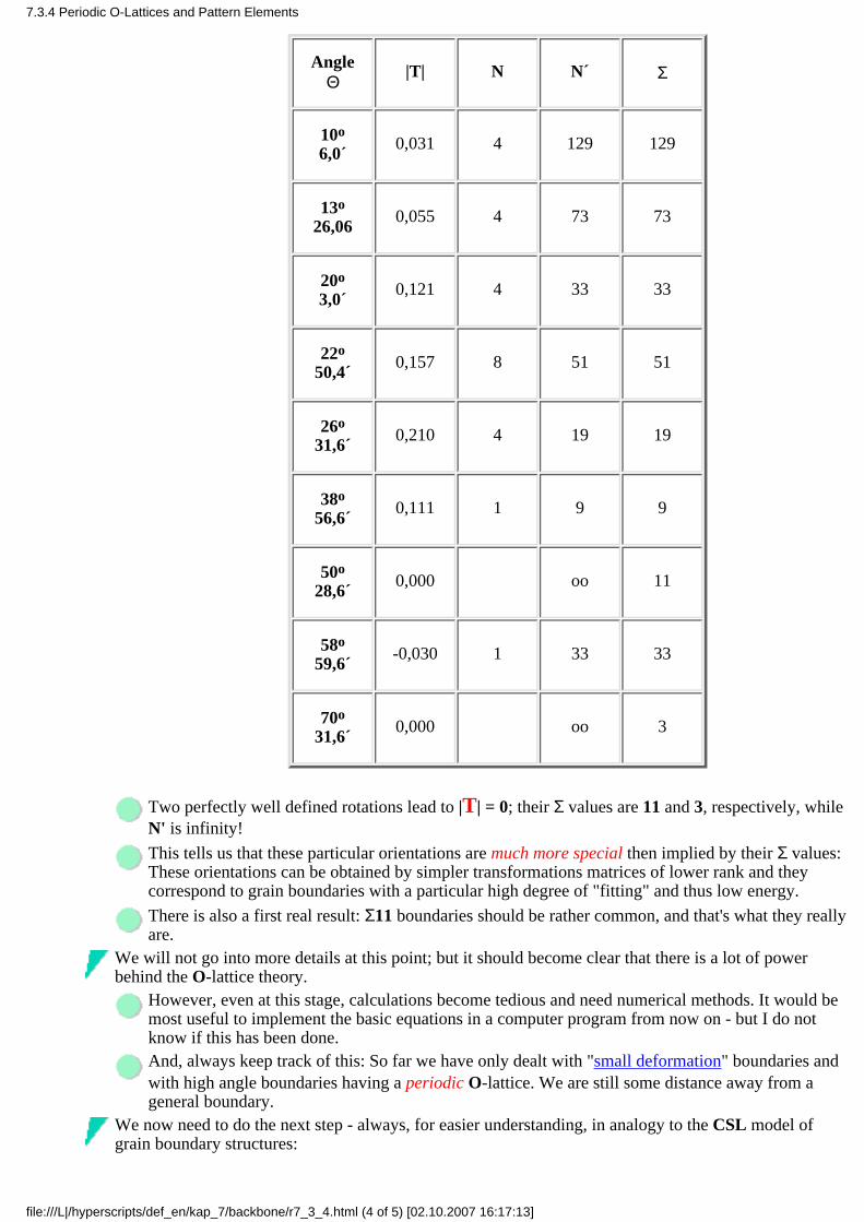
AngleΘ |T| N N´ Σ
10o
6,0´0,031 4 129 129
13o
26,060,055 4 73 73
20o
3,0´0,121 4 33 33
22o
50,4´0,157 8 51 51
26o
31,6´0,210 4 19 19
38o
56,6´0,111 1 9 9
50o
28,6´0,000 oo 11
58o
59,6´-0,030 1 33 33
70o
31,6´0,000 oo 3
Two perfectly well defined rotations lead to |T| = 0; their Σ values are 11 and 3, respectively, whileN' is infinity!
This tells us that these particular orientations are much more special then implied by their Σ values:These orientations can be obtained by simpler transformations matrices of lower rank and theycorrespond to grain boundaries with a particular high degree of "fitting" and thus low energy.
There is also a first real result: Σ11 boundaries should be rather common, and that's what they reallyare.
We will not go into more details at this point; but it should become clear that there is a lot of powerbehind the O-lattice theory.
However, even at this stage, calculations become tedious and need numerical methods. It would bemost useful to implement the basic equations in a computer program from now on - but I do notknow if this has been done.And, always keep track of this: So far we have only dealt with "small deformation" boundaries andwith high angle boundaries having a periodic O-lattice. We are still some distance away from ageneral boundary.
We now need to do the next step - always, for easier understanding, in analogy to the CSL model ofgrain boundary structures:
7.3.4 Periodic O-Lattices and Pattern Elements
file:///L|/hyperscripts/def_en/kap_7/backbone/r7_3_4.html (4 of 5) [02.10.2007 16:17:13]

What happens if the orientation of the two crystals (including arbitrary lattices and thus phaseboundaries, too) is close to, but not exactly at a "special" O-lattice orientation? "Special" meaning aperiodic O-lattice.In other words, we are asking for possible structural defects which can be superimposed and willchange the (generally non-periodic) O-lattice of an arbitrary boundary (which is always defined)just the right amount to generate a periodic O-lattice with a supposedly low energy?
This is the essentially the same question we asked for crystals close to, but not exactly at a " low Σ"orientation - but on a much higher level of abstraction and with the possibility to deal with itquantitatively.
7.3.4 Periodic O-Lattices and Pattern Elements
file:///L|/hyperscripts/def_en/kap_7/backbone/r7_3_4.html (5 of 5) [02.10.2007 16:17:13]
7.3.5 Pattern Shift and DSC Lattice
The General Idea of Pattern Element Conservation
In the CSL model of grain boundaries the DSC lattice was introduced to account for small deviationsfrom a perfect lattice coincidence orientation. It was the lattice of all translations of one of the crystalsthat conserved the given CSL. Translations other then those of the DSC lattice would destroy thecoincidence of lattice points.
The lattice vectors of the DSC lattice therefore could also be interpreted as the set of possibleBurgers vectors for dislocations allowed in a grain boundary without destroying the coincidence.While the simple recipe for constructing the DSC lattice in the simple cases usually shown(two-dimensional, cubic lattices) is rather straight forward, it was neither mathematically justified,nor is it immediately clear how it should be constructed in complicated cases.The DSC lattice, in fact, comes from the O-lattice theory and was simply adopted to the "easy"CSL model.
Obviously we now must ask ourselves: What happens to an O-lattice, particularly a periodic one, if wetranslate one of the crystals?
This is actually one of the more complicated questions to ask, especially for the rank of thetransformation matrix A < 3 (as we expect for grain boundaries).
We will not go into details here because in this rendering of O-lattice theory we omitted some moremathematical points considering what happens to the O-lattice in a given situation if you shift (=translate) crystal I or crystal II. Or, in a reversed situation, how you must shift crystal I or II if youtranslate the given O-lattice.
The first answer to the question above is:
In general (i.e. rank A = 3), the O-lattice is preserved, but shifted by some amount that depends onthe (arbitrary) magnitude of the translation of the crystal chosen.This is in contrast to the CSL,where arbitrary shifts not contained in the DSC lattice will completely destroy the CSL.This does not help, we obviously must find a more specific criterion than just conservation of theO-lattice in general in order to find specific translations that correspond to Burgers vectors of grainboundary dislocations. We therefore ask more specifically:
What happens to the pattern elements associated with every equivalence point in a reduced periodicO-lattice upon shifting one of the crystals?
Since we have seen (without proving it) that any O-point can be taken as the origin for the rotationtransforming crystal I into crystal II; we should be able to shift lattice I by any vector pointing to anequivalence point in the reduced O-lattice without changing pattern elements. In other words wesimply change the origin of the rotation (we only look at rotations in this examples).The O-lattice then will also be shifted by some other vector which can be calculated by employingour basic equation
(I – A–1) ri0 = T(I)
The ri are the base vectors of the O-lattice if we take Ti to be the set of base vectors of the crystal Ilattice.
Now shift the crystal I lattice by some vector e connecting equivalence points, replace ri by ri = r0i +
∆ri, with ∆ri = shift of the O-lattice for a shift e of the crystal lattice, and solve the equation for the ∆ri.
Well, lets not do it, but accept that there is a shift that can be calculated.
On second thoughts, this must also be true for lattice II. We thus may also employ vectors thattranslate lattice II by one of the vectors pointing to equivalence points in the reduced O-lattice.
7.3.5 Pattern Shift and DSC Lattice
file:///L|/hyperscripts/def_en/kap_7/backbone/r7_3_5.html (1 of 3) [02.10.2007 16:17:14]

And on third thoughts (not entirely obvious), we also must be able to translate the O-lattice itself byany vector that connects equivalence points. This requires that the O-lattice shifts by some vector -it is the reverse problem from the one outlined above.
The trick is that all those shifts may be different, and while they all produce the same general O-lattice,there might be different pattern elements. But - there is a finite number of pattern elements and a finitenumber of possible shifts.
Obviously, the set of all different configurations (distinguished by pattern elements) obtainabledefines the complete geometry of the particular boundary with the periodic O-lattice consideredbecause no configuration is special.The set of all possible displacement vectors can be expressed as the translation vectors in a newkind of lattice, the "Complete Pattern Shift Lattice", abbreviated by Bollmann as " DSC lattice",that we encountered earlier (in a much simpler form).
Unfortunately, it is not immediately obvious how to calculate the DSC lattice from O-lattice theory. Infact, the respective chapter in Bollmanns book is particularly hermetic or obtuse.
Somewhat later (1979), Bollmann together with Pond gave the old abbreviation a new meaning:"DSC" now stands for "Displacements which are Symmetry Conserving". But few people knowwhat exactly DSC stands for - the main thing is to understand the significance of the DSC lattice.
Some Illustrations
Lets see what the various displacements discussed above really produce if applied to a simple situation.We take the (redrawn) example from Bollmanns book.
First, lets construct the possible set of pattern conserving translations by putting several reducedO-lattice cells together (for the case of rotation around <100> of 39o 52,2´, corresponding to the Σ= 5 CSL).
The left part shows the rotation, yielding the O-lattice. Coinciding lattice points that are alsoO-points are shown in green, the other O-points in red. On the right-hand side the repeated reducedO-lattice is shown in the blue crystal.
Now lets displace the brown lattice by a vector pointing form the green to the red equivalence point inthe above picture. Here is what you get.
7.3.5 Pattern Shift and DSC Lattice
file:///L|/hyperscripts/def_en/kap_7/backbone/r7_3_5.html (2 of 3) [02.10.2007 16:17:14]

The O-lattice shifted down, and some newkinds of pattern elements appear. Thereare no more or less special than the onesin the picture above; both belong to thecomplete structure of the boundaryillustrated.
Note that we also obtain new equivalencepoints for the boundary (in the middle ofthe lines defining the square lattices).
Now we shift the brown lattice by one of the vectors pointing to the new equivalence point. Weobtain yet another pattern element.
But that's it. The pattern elements shownhere are all there are (Try to prove thatyourself if you don't believe it).
We could now start to produce the DSClattice, but this will just give the samekind of lattice we had in the simple CSLcase.
Instead we only note that there is a sufficiently clear procedure of how to create a DSC lattice for agiven periodic O-lattice, that is always applicable - even to phase boundaries (in principle; of courseonly in principle).
In the next (and last) chapter, we will show how O-lattice theory now can be applied to large anglegrain boundaries and discuss briefly its merits and limits.
7.3.5 Pattern Shift and DSC Lattice
file:///L|/hyperscripts/def_en/kap_7/backbone/r7_3_5.html (3 of 3) [02.10.2007 16:17:14]

7.3.6 Large Angle Grain Boundaries and Final Points
Application of O-Lattice Theory to Large Angle Grain Boundaries
The basic assumption is that an arbitrary grain boundary would prefer to be in a orientationcorresponding to a periodic O-lattice with a high density of equivalence points. This is a fancy (i.e. moregeneral) way for saying that boundaries prefer to be in a low Σ orientation as we did in the simple CSLmodel.
Such a particular orientation can be achieved at the expense of generating some grain boundarydislocations.For a small angle grain boundary we have seen that a cut of the boundary plane through theO-lattice gives directly the geometry of the dislocation network (give or take some adjustments toaccount for the particular dislocation properties).The O-lattice was obtained (by calculations) relative to the two real crystals. Looking back, whatwe did was to use one of the crystals as a reference for the preferred state, the other one thendescribed the deviation of the boundary from the preferred state.
For large angle grain boundaries we now do exactly the same thing - except that the reference state isnow the periodic O-lattice that the boundary aspires to obtain.
The deviation of the boundary from this preferred state is then described by the O-lattice that comeswith the orientation that describes the actual boundary .
The logical consequence then is that the geometry of the dislocation network necessary to obtain thepreferred state is the O-lattice of the two O-lattices described above - a so-called O2-lattice or secondorder O-lattice.
That may sound a bit heavy, but it is really straight forward if you think about it.
It is also clear - in principle - how we would calculate the O2-lattice, but we are not going to look atthis.
If we now imagine a boundary plane cutting through our O2-lattice as before, we now must ask howlarge the translation will be that the O-lattice "crystals" experience when a O2-lattice wall is crossed.This translation will be the Burgers vector of the second-order dislocation forming the grain boundarydislocation network.
Well, as you would have guessed, it must be a translation that conserves the underlying pattern ofthe O-lattices, so the translation vector (= Burgers vector) is a vector from the DSC-lattice of one ofthe primary O-lattices.While our periodic reference O-lattice has a defined DSC lattice, the other one may (and in fullgenerality probably will) have a non-periodic O-lattice and thus does not have a DSC lattice. Thislooks like a problem.However, since O-lattices are continuous (and smooth) functions of the misorientation angle (whichthe CSL is not), we know that the two O-lattices are rather similar, and we always can take theDSC lattice of the periodic O-lattice in a good approximation. So there is no real problem.
OK. We are done. That's (almost) all there is to it.
The general recipe for constructing a grain boundary with a secondary is network is "clear". It goesexactly along the lines we derived for small angle grain boundaires - only we work in "second orderO-lattice theory".The reverse is also possible: We have a general recipe for analyzing the structure found in a realboundary.It will just take a few months of studying the intricacies of the underlying math and some gettingused to the more trickier thoughts, and you can construct and analyze all kinds of boundaries onyour own.
But most likely, you won't. This is due to some (sad) facts of life that will be the last thing to discuss inthis context.
Merits and Limitations of O-Lattice Theory
7.3.6 Large Angle Grain Boundaries and Final Points
file:///L|/hyperscripts/def_en/kap_7/backbone/r7_3_6.html (1 of 2) [02.10.2007 16:17:14]

The merits of Bollmanns theory are clear:
It nucleated a lot of work on grain boundary structures and introduced the crucial concept of theDSC lattice and its dislocations.It was (and is) the mathematical frame work for tackling the kind of higher-level geometry that iscontained in interfaces between crystals. (It will be interesting to see if someone sometime tacklesthe grain boundary structure between single quasi-crystals, which could be done by extendingO-lattice theory into a 6-dimensional space and then project the results back into three dimensionalspace).It allows to conceive and analyze more complex problems, where a CSL model is not sufficient.
However, there are serious problems and limitations, too.
The recipe for the proper choice of the one transformation matrix you should use out of manypossible ones is not always correct. It generally fails for (some) small angle tilt boundaries, wherethe O-lattice theory would predict a twin-like structure with no dislocations - contrary to theobservations. It also fails for some other boundaries, casting some lingering doubt on the wholething.It is still too simple to account for real boundary structures even if the limitation referred to abovedoes not apply. Two examples might be mentioned.1. The rigid body translations observed in many (twin-like) boundaries, especially in bcc lattices.
2. Tremendously complicated structures observed in crystal with more than one atom in the base ofthe crystal - e.g. in Si. What happens (and was first observed and then analyzed by Bollmann) isthat dislocations in the DSC lattice may split into partial dislocations bounding a stacking fault inthe DSC lattice. While this effect may be incorporated into the O-lattice theory, it does not make iteasier.
Still, whereas newer theories concerned with the structures of grain boundaries do exist, none is quite ascomplete and mathematical as the O-lattice theory. A "final" theory has not yet been proposedWhat remains for practical work is
The DSC lattice. This is certainly the most important outgrowth of the O-lattice theory. Grainboundaries simply cannot be discussed without reference to the DSC lattice. For practicalimportance it has all but eclipsed the O-lattice. As we have seen, it is (mostly) easily constructedwithout going into heavy matrix algebra.The systematic approach, always good for looking deeper into less clear situations.
The good feeling, that something can be done about taking a deep look into grain boundarystructures from a theoretical point of view, even if there are some limitations and unclear points.
7.3.6 Large Angle Grain Boundaries and Final Points
file:///L|/hyperscripts/def_en/kap_7/backbone/r7_3_6.html (2 of 2) [02.10.2007 16:17:14]

8. Phase Boundaries
8.1 Misfit Dislocations
8.1.1 Modifications of the CSL Concept and Misfit Dislocations
8.1.2 Energy of Misfit Dislocations and Critical Thickness
8.1.3 Other Defects in Phase Boundaries
8.2 Case Studies
8.2.1 Ni Silicides
8.2.2 Case Study for Pd Silicides
8.3 Steps in Interfaces
8.3.1 The Relation Between Steps and Dislocations in Σ = 3 Boundaries
8.3.2 Open Questions
Contents of Chapter 8
file:///L|/hyperscripts/def_en/kap_8/backbone/r8.html [02.10.2007 16:17:14]

8. Phase Boundaries
8.1 Misfit Dislocations
8.1.1 Modifications of the CSL Concept and Misfit Dislocations
The O-lattice theory fully accounts for the structure of phase boundaries, too - as long as we look at twocrystalline phases, of course. It is, however still not easy to use (it is waiting for someone to turn it into auser-friendly piece of software), and it can not answer a few specific question about the development ofthe structure whenever a phase boundary is formed.So for phase boundaries, too, it is often more easy to think in terms of the simpler coincidence lattice -but with a grain of salt. A few special points are:
In general, there will be no suitable coincidence lattice at all, because the lattices are different andtheir lattice constants are incommensurable (their quotient is an irrational number). In practice,however, we do not know the lattice constants to an arbitrary degree of precision, and you willalways find some fitting relation.Even if there is a CSL, it is not necessarily the proper reference lattice. This can be seen from asimple example: Two cubic crystals with lattice constants a1 = 1 and a2 = 1,05 (i.e. a misfit of 5%)from a phase boundary:
We have a perfect two-dimensional CSL structure (Σ2d = 20 would hold for 2 dimensions),
Note that we can have situations (like even Σ numbers) which are simply not possible for grainboundaries, where the lattice constants are the same by definition.
It is much more sensible to describe this phase boundary as a Σ = 1 boundary with superimposed phaseboundary dislocations (which we practically always will call misfit dislocations) as shown below,because this is usually an energetically better situation than a Σ2d = 20 (or whatever) boundary with nodislocations.
The misfit dislocations in this case are more or less lattice dislocations of the crystals - but that doesnot mean that DSC lattice dislocations never occur in phase boundaries!
8.1.1 Phase Boundaries
file:///L|/hyperscripts/def_en/kap_8/backbone/r8_1_1.html (1 of 5) [02.10.2007 16:17:14]

Misfit dislocations compensate for differences in the lattice constants by concentrating the misfit inone-dimensional regions - the dislocation lines.
Between the dislocation lines the interface is coherent; a phase boundary with misfit dislocations iscalled semi-coherent.Misfit dislocations - in contrast to general grain boundary dislocations - must have an edgecomponent that accounts for the lattice constant mismatch
Whereas the O-lattice theory as applied to phase boundaries allows phase boundary dislocations ingeneral (of which misfit dislocations are only a subset), "simple" misfit dislocations are the dominantdefects in technologically important man-made phase boundaries.
Misfit dislocations are not restricted to boundaries between two chemically different types ofmaterials. Silicon heavily doped with, e.g., Boron, has a slightly changed lattice constant and thusformally can be sen as a different phase. The rather ill defined interface between a heavily dopedregion and an undoped region thus may and does have misfit dislocations, an example is given inthe illustration.The mere existence of misfit dislocations coupled with their usually detrimental influence onelectronic properties is the reason why many "obvious" devices do not exist at all (e.g.optoelectronic GaAs structures integrated on a Si chip), and others have problems. The aging ofLaser diodes, e.g., may be coupled to the behavior of misfit dislocations in the many phaseboundaries of the device.Optoelectronics in general practically always involves having phase boundaries, e.g. devices likeLasers, LEDs, as well as all multi quantum well structures. A very careful consideration of misfitand misfit dislocations is always needed and some special process steps are often necessary to avoidthese defects.
However, not every (Σ = 1) phase boundary with some misfit between the partners contains misfitdislocations - provided one of the phases consists of a thin layer on top of the other phase. Only if thethickness of the thin-layer phase exceeds a critical value, misfit dislocations will be observed. It is easyto understand why this is so:
For thin layers, it may be energetically more favorable to deform the layer elastically, so that aperfect match to the substrate layer is achieved. The total elastic energy contained in the "strainedlayer" scales with the thickness of the layer and the expenditure in elastic energy below a criticalthickness for an epitaxial layer may be smaller than the energy needed to introduce misfitdislocations.
This is a situation not dealt with in the O-lattice theory or its simple CSL version. A new theory isneeded.
8.1.2 Energy of Misfit Dislocations and Critical Thickness
The critical thickness for the introduction of misfit dislocations can be obtained by equating the energycontained in a misfit dislocation network with the elastic energy contained in a strained layer ofthickness h.
Since the elastic energy increases directly with h, whereas the energy contained in the dislocationnetwork increases only very weakly with h, the thickness for which both energies are equal is thecritical thickness hc. Thicker layers are energetically better off with a dislocation network, thinnerlayers prefer elastic distortion.This computation was first done by Frank and van der Merve in 1963; the resulting Frank andvan der Merve formula became quite famous.
Somewhat later in 1974 Matthews and Blakeslee reconsidered the situation and looked at the forcesneeded to move a few pre-existing dislocations into the interface in order to form the misfit dislocationnetwork. They obtain the same formula for the critical thickness as van der Merve (i.e. the equilibriumsituation), but their treatment also allows to consider the kinetics of the process to some extent (i.e. howthe network is formed) and is therefore widely used.
8.1.1 Phase Boundaries
file:///L|/hyperscripts/def_en/kap_8/backbone/r8_1_1.html (2 of 5) [02.10.2007 16:17:14]

We are looking at the situation retrospectively by studying an article of the possibly most famousTEM and defect expert, Peter Hirsch from Oxford University, or, to be precise, Sir Peter as hemust be called after his nobilitation by Elizabeth I, Queen of England.This is to show that - honorwise - a defect expert can go just as far as a rock star (several of whichhave been knighted by the queen - most famous the Beatles). Moneywise, however, it is acompletely different matter.We use parts of his article printed in the Proceedings of the 2nd International Conference onPolycrystalline Semiconductors (Schwäbisch Hall, Germany, 1990, p. 470). Do look it up - it is partof the lecture!
As you saw, great minds sometimes make great steps and are not immune to small errors! If you didn'tsee that, consider:
How exactly do you get eq. 1?
Why is the strain for minimum energy calculated in eq. 3 equal to the unrelaxed elastic strain at thepoint of the introduction of dislocations?What is h, the thickness of the layer, doing in an equation for the critical thickness hc (eq. 5)? Afterall, the critical thickness can not possibly depend on the thickness itself.
Well, if you want to know, turn to the annotated version of Sir Peters paper.
Still, Sir Peter got it right in principle, and his derivation of the critical thickness is short and mostelegant. The final formula for the critical thickness hc is
hc = b
8π · f · (1 + ν) · ln
e · hc
r0
With b = Burgers vector of the misfit dislocations (actually only their edge component in the planeof the interface), f = misfit parameter, i.e ∆a/a, e = e = 2,7183... = base of natural logarithms, andr0 = core radius of the dislocations.
This transcendental equation may be roughly approximated by
hc ≈ b
9.9 · f
Lets see what the calculations tell us for real phase boundaries (for a b value of 0.376 nm (which appliesto Si)). We note that misfit dislocations are only to be expected if the layer thickness h exceeds thecritical value hc.
8.1.1 Phase Boundaries
file:///L|/hyperscripts/def_en/kap_8/backbone/r8_1_1.html (3 of 5) [02.10.2007 16:17:14]

For a misfit of 1% the critical thickness is about 4 nm - not much at all!
This situation provides for many technological problems, especially in semiconductor technology. Itimposes severe limits on "heterojunctions", i.e. electronic junctions between two materials because amisfit dislocation network will invariably "kill" your device - if not immediately, somewhat later (whichis often worse!).
Looking at common technical semiconductors, we realize that we have major problems in makingheterojunctions:
Misfits between two materials tends to be large (not even considering Si with a lattice constant of a= 0,532 nm), and dislocation free interfaces do not come easy, if at all.A large group of researchers has been (and still is) looking for ways to beat the critical thicknesslimitations. There are many tricks (the link contains a few), but hard work is needed just as much assome luck and good ideas. A particularly clever recent idea known under the heading of"compliant substrates" is described in an advanced module.
Experiments confirm the theory. Very thin epitaxial layers of a second phase do not show dislocations inthe interface, but with increasing thickness misfit dislocations will appear.
Considering that misfit dislocations are usually unwanted but that they must appear with increasinglayer thickness - however not out of thin air - we ask an important question:
8.1.1 Phase Boundaries
file:///L|/hyperscripts/def_en/kap_8/backbone/r8_1_1.html (4 of 5) [02.10.2007 16:17:14]

Exactly how are misfit dislocations produced and incorporated into the interface if the critical thicknessis reached. More to the point: How can I prevent this nucleation and migration process?
Suffice it to say that while this question has not been fully answered, there are many ways andtricks to keep misfit dislocations from appearing at the earliest possible moment.The issue is sufficiently important in optoelectronics to merit more discussion. More information tothis point can be found in various modules of the Hyperscript "Semiconductors".
8.1.3 Other Defects in Phase Boundaries
Even coherent phase boundaries can still contain other defects besides misfit dislocations (not tomention incoherent phase boundaries). In particular, we must expect:
Dislocation networks besides the misfit dislocations that compensate for small tilt and twistcomponents in analogy to the small angle grain boundaries.Steps associated with dislocations (so-called incoherent steps) in analogy to the steps encounteredin grain boundaries.
Coherent steps (without any dislocation character) as something new.
After all, the surface of a substrate on which we deposit a layer of a second phase will, in general, not beatomically flat. Steps thus must be expected to be an integral part of the phase boundary. We willexamine some examples for this in the next subchapter.
Next, it is important to realize that semicoherent phase boundaries can have other CSL relation besidesΣ = 1, in particular Σ = 3, but other values, too.
As the most important example, consider a hexagonal lattice matched to the {111} plane of a fcclattice. It is found to be in a Σ = 3 relationship, easily seen if you compare the stacking sequences inthe picture below:
The ACACACA... stacking sequence of the hexagonal lattice fits right on the ABCABCA..stacking sequence of the fcc lattice on a {111} plane. The Σ = 3 relationship is clearly visible; it isindicated by red dots and lines.There are of course more complex geometries - if the CSL concept is not applicable; the O-latticeconcepts has to be used.
Sorting out the various types of possible defects is no longer an easy task. The interpretation of TEMmicrographs may become quite involved.
Some examples will be discussed in the case studies in the next subchapter.
8.1.1 Phase Boundaries
file:///L|/hyperscripts/def_en/kap_8/backbone/r8_1_1.html (5 of 5) [02.10.2007 16:17:14]

8.2 Case Studies
8.2.1 Ni Silicides
We will look in some detail on the system Si - silicide - metal, where many phase boundaries can beobserved. The basic experiment consists of depositing a metal (here Ni) on Si (either in a {100} or {111}orientation), and induce some reaction by heating.
Three different Ni-silicides will form consecutively:
Altogether five different phase boundaries may be encountered, some of which are shown in the pictureabove:
Si - Ni,Si - Ni2Si and Ni2Si - Ni,Si - NiSi and NiSi - Ni2Si,Si - NiSi2, and NiSi2 - NiSi.
Major findings are:
The interface between Si and Ni does not really exist because immediately after the (roomtemperature) evaporation, a thin Ni2Si-silicide layer forms between the Si and the Ni.
The Ni2Si layer is polycrystalline; the interface between Si and Ni2Si seems to be incoherent - i.e. ifthere is any structure it is not observed with "normal" TEM.
The interface between {111} Si and NiSi is epitaxial, however, and thus semicoherent against allexpectations:
NiSi is reported to crystallize in an orthorhombic lattice; on {111} Si substrates, however, ahexagonal lattice is observed (which can be cobtained from an orthorhombic lattice by slightadjustments of the lattice parameters).The misfit is extremely large (ca. 15%) and would require a distance of 0,6 nm for b = a/2<110>misfit dislocations. Such a small spacing is usually considered to be too small to be meaningful -epitaxial relationships thus should not exist. The diffraction pattern, however, indicates a clearepitaxial relationship (with a bit of polycrystallinity as indicated by the rings):
8.2.1 Case Studies
file:///L|/hyperscripts/def_en/kap_8/backbone/r8_2_1.html (1 of 4) [02.10.2007 16:17:15]

While no structure can be seen in conventional TEM, high-resolution TEM shows pronouncedmisfit dislocations relieving some of the stress at a spacing of about 1,6 nm. This is one of thedensest misfit dislocation networks ever observed. The ending lattice planes are indicated by theedge dislocation symbol somewhat above the actual interface plane.
The most interesting phase is NiSi2; it is the final product after sufficient annealing at 800 °C.
NiSi2 crystallizes in the cubic CaF2 - structure with a lattice constant that is only 0,3% smaller than
that of Si.We thus can expect an epitaxial relationship with a misfit dislocation network at a spacing
p = b ·b
(ae – am)/am =
b
0,003
With aSi = 0,54 nm and b = a/2<110> = 0,382 nm we would expect a network with a spacing ofabout 130 nm.What we see for an interface on a {111} plane looks like this:
8.2.1 Case Studies
file:///L|/hyperscripts/def_en/kap_8/backbone/r8_2_1.html (2 of 4) [02.10.2007 16:17:15]

This looks rather interesting. We seem to have a simple hexagonal network of dislocations, but wesee some additional features: "Blackish" areas and an island with rather coarser structuresembedded in a sea of something with a possible hexagonal symmetry.
The reasons for these complications are two peculiarities of this interface, which can also be found insimilar systems; in particular in the Si - CoSi2 interface.
First, it "likes" to be on {111}-planes. This leads to heavy facetting if the Ni layer is deposited on aSi {100} plane, but also to some facetting on {111}. This can be seen best in cross-section; anexample is given in the illustration. We must expect that the accommodation of steps will introduceirregularities into the network.
Second, the interface is mostly not in a Σ = 1 relation, i.e. with a direct continuation of the lattices,but in a Σ = 3 relation. This means that the NiSi2 is twinned with respect to the substrate. Anoverview picture is shown in the link. This somewhat surprising result can be obtained from acareful contrast analysis of the network with micrographs taken at higher magnifications. Thenetwork then looks like this:
8.2.1 Case Studies
file:///L|/hyperscripts/def_en/kap_8/backbone/r8_2_1.html (3 of 4) [02.10.2007 16:17:15]

Shown is one of the "islands" in a sea of regular hexagonal dislocations. Its structure lookssomewhat familiar: The arrows point to extended stacking fault knots as in the case of the smallangle twist grain boundary on {111} in Si.But in contrast to the network in the small angle twist boundary, all dislocations now are edgedislocations; as expected for misfit dislocations. The distance is also what would be expected for aalmost fully relaxed layer of NiSi2.
The question is, of course, why this mix of Σ = 1 and Σ = 3 relations? As in the case of the low angletwist boundary encountered before, nobody knows for sure. Obviously, the energy balance is rathersimilar for the two cases.
Very similar interfaces have been observed in the case of Si - CoSi2 interfaces, which, except for aslightly larger misfit, have essentially the same geometry.
Despite the structural similarity to the small angle grain boundaries, the phase boundaries add newfeatures and open questions. To get more insights, we will now discuss the case of the interface between(cubic) Si and (hex.) Pd2Si.
8.2.1 Case Studies
file:///L|/hyperscripts/def_en/kap_8/backbone/r8_2_1.html (4 of 4) [02.10.2007 16:17:15]

8.2.2 Case Study for Pd Silicides
If Pd instead of Ni is evaporated on a clean Si surface, hexagonal Pd2Si (a = 0,653 nm, c = 0,344 nm)develops around 200°C - 300°C. Increasing the annealing temperatures produces no new phases.
The misfit of the hexagonal {001} plane to a Si {111} plane is 1,8%; we can expect an epitaxialrelationship with a misfit dislocation network at a spacing of about 10 nm. This is around theresolution limit of TEM in a regular contrast mode, so we have to resort to HRTEM andcross-sectional specimen.A HRTEM image of the interface is shown below (This picture from 1980 is of historical interest,too: It was, to the best of my knowledge, the first HRTEM picture ever obtained from a phaseboundary).
We clearly have an epitaxial layer of Pd2Si. No ending lattice fringes denoting misfit dislocations areunambigously visible. Therefore a Burgers circuit has been drawn, somewhat analogous to theprocedure used to obtain Franks formula. It goes up in the Pd2Si, then to the left crossing 90 latticefringes, back to the boundary, 90 fringes to the right and up to the boundary again. It does not close,although it is clear that it would have closed on a perfectly flat and misfit-dislocation free interface.
Does this mean that the phase boundary contains misfit dislocations?
This is not clear. We may have dislocations in the interface, but we certainly have steps as can beseen directly. We now have to pay some attention to the relationship of dislocations and steps, theirimages in a HRTEM picture, and their consequences for a Burgers circuit.
This will lead us into new and quite complicated territory. We will consider the relationship betweensteps and dislocations only for the example of hexagonal lattices on cubic lattices, or, more generally,for Σ = 3 relations. This will be sufficient to gain an idea of the added complexity.
8.2.2 Pd Silicides
file:///L|/hyperscripts/def_en/kap_8/backbone/r8_2_2.html [02.10.2007 16:17:16]

8.3 Steps in Interfaces
8.3.1 The Relation Between Steps and Dislocations in Σ = 3 Boundaries
Playing with models of a perfectly fitting phase boundary between a hexagonal and a cubic lattice, onerealizes quickly that steps can be incorporated without problems and without dislocations as long as thestep height comes in multiples of 3 (in units of the translation vectors of the CSL). This, together withsome other cases, is shown below:
The left two pictures show pure steps (or coherent steps). For ease of interpretation, some latticeplanes of the DSC lattice are shown in blue; ending lattice planes of the DSC lattice are red. Endinglattice fringes, as seen on a HRTEM micrograph, are indicated in light blue - note that they are notthe same thing as lattice planes. The phase boundary itself is shown in light green.Included in the drawing are also two pure DSC lattice dislocations (middle pictures). They are truedislocations because they can be constructed with the Volterra method as demonstrated before, andthey have the 1/r stress field that is a hallmark of dislocations. Sometimes they are calledcoherency dislocations.Finally, a mix of pure dislocations and pure steps is shown on the right. It is evident that steps goingjust one plane up or down must be a mix of pure steps and pure dislocations. The same is true forsteps going 4 planes up or down and so on. These dislocations are sometimes calledanti-coherency dislocations.Note that there is no way of having a combination of pure steps and dislocations with step heightzero.
An unexpected property emerges: Pure steps (sometimes also called coherent ledges) show endinglattice fringes in a HRTEM micrograph, whereas true dislocations in this case are not associated withending lattice fringes.
Where does that leave us? Is Franks formula, which after all counted Burger vectors in a circuit notunlike the one shown before, not applicable to non-planar boundaries? Why can we see endinglattice fringes in a TEM picture and there is no dislocation?Well, ending lattice fringes (again note we call it lattice fringe on purpose) are not lattice planes,and at a grain- or phase boundary all lattice planes of one kind end and some of a new kind start.The fact that some visible fringes appear to be continuous in a "fuzzy" projection of the lattices, hasno particular meaning in itself. Of course, one lattice plane ending in one crystal may give rise to alattice fringe ending on a micrograph, too, and thus signify an edge dislocation, but this must not begeneralized.
We may, however, make an important generalization of a different kind: A semi-coherent phase or grainboundary, in general, needs at least two qualitatively different kinds of defects in its interface:
Pure DSC-lattice dislocations (generally associated with an intrinsic step), and
8.3.1 Steps in Interfaces
file:///L|/hyperscripts/def_en/kap_8/backbone/r8_3_1.html (1 of 4) [02.10.2007 16:17:16]

Pure steps (without dislocation character, i.e. without a long range stress field).
In general both defects are required as we will see if we now compose a (hexagonal) dislocation networkin a Σ = 3 boundary.
Whereas the dislocation network has a perfect threefold rotational symmetry, the boundary is lesssymmetric. This can be seen when we consider the steps introduced by the dislocations (use thepicture above), too:
As soon as we defined the line- and Burgers vectors, we realize that the steps associated with puredislocation are always the same: Looking in the line direction, crossing a pure dislocation wouldalways lead two steps down in this example. If we start a closed circuit at the hexagon labelled"(level) 1" and go across the green dislocation, we end up two atomic planes down on level 3. Thesame happens if we now cross the blue dislocation; we are down to level 5.However, in closing the circuit, we must necessarily come up to level 1 again, This is only possibleif the dark red dislocations break the symmetry and contain two steps (–2 + 6 = 4). Thus we go twolevels down and 6 levels up, which is just right.
This feature, which is clearly a general feature of all boundaries, opens up a whole new can of worms.
There is more than one way to combine pure steps and pure dislocations to create a network thatsatisfies the requirements for accommodating misfit (this needs the dislocations) and to compensatefor the steps introduced by the dislocations (this needs pure steps).The image of a given boundary in cross-sectional HRTEM can look very different, depending onwhat kind of possible configuration is cut which way. Lattice fringes may end in several differentways. The closing failure of a Burgers circuit that counts lattice fringes around a large part of an interfacethus cannot be considered as a net count of dislocation Burgers vectors. Combined with a net countof the steps in the interface, however, it may be useful.The following graphic illustrates these points
8.3.1 Steps in Interfaces
file:///L|/hyperscripts/def_en/kap_8/backbone/r8_3_1.html (2 of 4) [02.10.2007 16:17:16]

Shown are two possible combinations of dislocations and steps in Σ = 3 boundaries (of any kind).Dislocations in combination with a coherent step are indicated in bold lines; the numbers in thehexagons indicate the level of the boundary
Two possible geometries are shown in the upper left-hand corner and the lower right-hand corner
Four cross-section through the dislocation/step network are drawn in together with their schematicimage in HRTEM. Ending lattice fringes are indicated in light blue (assuming without justificationthat the image of dislocation/step combinations that are inclined with respect to the electron beamadd no further complications).
It becomes clear that the interpretation of an HRTEM image can be a demanding task which will notnecessarily give an unambiguous answer. You may try your skills at the picture in the illustration.
But we are still not done with the discussion of the intrinsic geometry of a simple Σ = 3 boundary. Evenif we assume that we have a dislocation/step network of a defined kind (e.g. the one from the upperleft-hand corner of the above drawing) and that the boundary is flat apart from the ups and downs of thedislocations, we must expect an added complication:
Since the dislocations/step network most likely formed in small patches and then spreads out,individual patches may be out of "synch", i.e. whenever they meet they will not fit together. This isillustrated below
8.3.1 Steps in Interfaces
file:///L|/hyperscripts/def_en/kap_8/backbone/r8_3_1.html (3 of 4) [02.10.2007 16:17:16]

Dislocations in combination with a coherent step are shown in bold; the color now denotes if thestep goes up or down as seen from the inside of the hexagons completely enclosed by "bold"dislocations. The dislocations/step network on the left and right side are identical, but displacedrelative to each other by one hexagon.Along the white line, they obviously don't match. We would need dislocations with a step height ofzero, which as we have seen before, do not exist in this geometry.
The only way out is to postulate a new kind of defect, some kind of stacking fault in the dislocation/steplattice. To the best of my knowledge, such a defect has not yet be named or discussed in detail -although it is clearly a necessary feature of general phase- or grain-boundaries.
This serves to illustrate that the last word about structural aspects of defects in crystal has not yetcome in. One may ask, of course, if esoterica like the dislocation/step network considerations are ofany importance. The answer is: Who knows?Considering however, that many materials (including natural minerals) are full of phase and grainboundaries, that many properties of theses boundaries are directly linked to their structure and thatnot much is known about the atomic structure of non-trivial boundaries, it is not totally unrealisticto expect that research will go on.
In the next (and last) subchapter we will briefly look at some more questions in relation to phaseboundaries.
8.3.1 Steps in Interfaces
file:///L|/hyperscripts/def_en/kap_8/backbone/r8_3_1.html (4 of 4) [02.10.2007 16:17:16]

8.3.2 Open Questions
The final conclusion in the phase boundary chapter is simple: There is still much to do! Some openquestions will just be mentioned:
If the phase boundary moves into the interior of some material in a reactive process like silicideformation, the phase boundary dislocations must climb. How do they do this?Supposedly, the climb of phase boundary dislocations needs a specified current of point defects(whatever is needed to accommodate the climb rate given by the speed of the advancing interface).Will the point defects assisting climb affect the kinetics of the phase boundary movement? How?
Does the hexagonal dislocation network have a preferred direction. How can this be proven?
What kind of defect forms the boundary between different network domains?
Many more questions can be formulated to understand just the structural properties of interfaces ingeneral. But here I stop. I have done my share of the work. Now it is up to you.
8.3.2 Open Questions
file:///L|/hyperscripts/def_en/kap_8/backbone/r8_3_2.html [02.10.2007 16:17:16]