Embed Size (px)
Citation preview
Kai Nordlund, Department of Physics, University of Helsinki
Nano-2
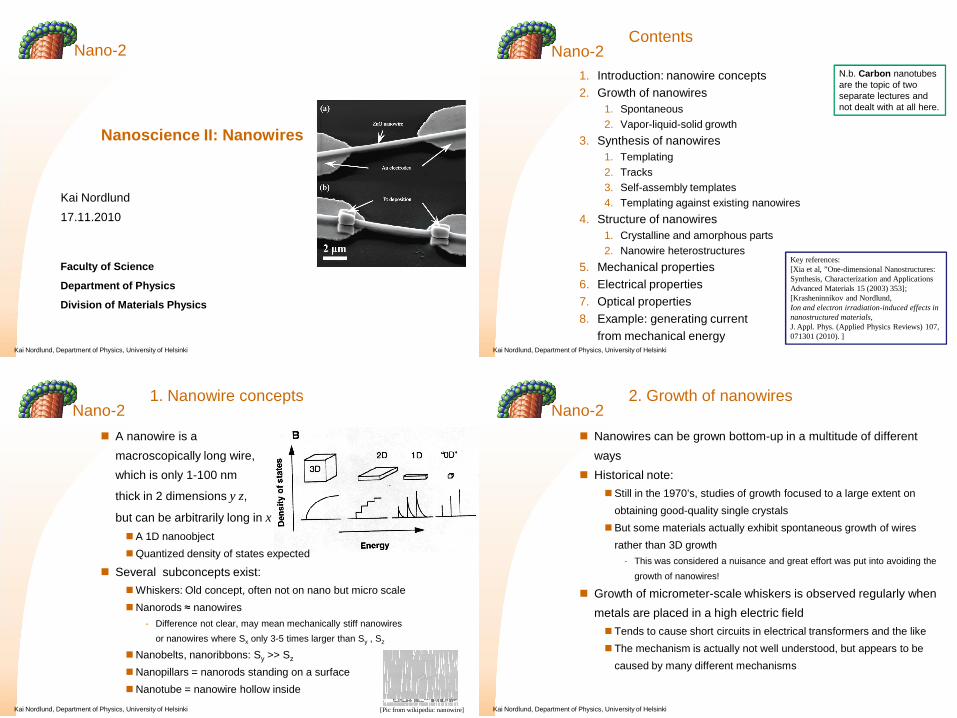
Nanoscience II: Nanowires
Kai Nordlund17.11.2010
Faculty of Science
Department of Physics
Division of Materials Physics
Nano-2
Kai Nordlund, Department of Physics, University of Helsinki
Contents
1. Introduction: nanowire concepts2. Growth of nanowires
1. Spontaneous2. Vapor-liquid-solid growth
3. Synthesis of nanowires1. Templating2. Tracks3. Self-assembly templates4. Templating against existing nanowires
4. Structure of nanowires1. Crystalline and amorphous parts2. Nanowire heterostructures
5. Mechanical properties6. Electrical properties7. Optical properties8. Example: generating current
from mechanical energy
N.b. Carbon nanotubesare the topic of two separate lectures and not dealt with at all here.
Key references:[Xia et al, ”One-dimensional Nanostructures:Synthesis, Characterization and ApplicationsAdvanced Materials 15 (2003) 353];[Krasheninnikov and Nordlund, Ion and electron irradiation-induced effects in nanostructured materials, J. Appl. Phys. (Applied Physics Reviews) 107, 071301 (2010). ]
Nano-2
Kai Nordlund, Department of Physics, University of Helsinki
1. Nanowire concepts
A nanowire is a macroscopically long wire,which is only 1-100 nm
thick in 2 dimensions y z,
but can be arbitrarily long in xA 1D nanoobjectQuantized density of states expected
Several subconcepts exist:Whiskers: Old concept, often not on nano but micro scaleNanorods nanowires
- Difference not clear, may mean mechanically stiff nanowiresor nanowires where Sx only 3-5 times larger than Sy , Sz
Nanobelts, nanoribbons: Sy >> Sz
Nanopillars = nanorods standing on a surfaceNanotube = nanowire hollow inside
[Pic from wikipedia: nanowire]
Nano-2
Kai Nordlund, Department of Physics, University of Helsinki
2. Growth of nanowires
Nanowires can be grown bottom-up in a multitude of different waysHistorical note:
Still in the 1970’s, studies of growth focused to a large extent on obtaining good-quality single crystalsBut some materials actually exhibit spontaneous growth of wires rather than 3D growth
- This was considered a nuisance and great effort was put into avoiding the growth of nanowires!
Growth of micrometer-scale whiskers is observed regularly when metals are placed in a high electric field
Tends to cause short circuits in electrical transformers and the likeThe mechanism is actually not well understood, but appears to be caused by many different mechanisms
Nano-2
Kai Nordlund, Department of Physics, University of Helsinki
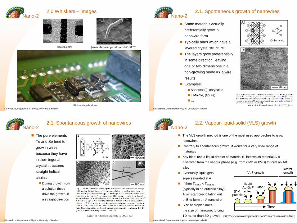
2.0 Whiskers – images
[www.efsot-europe.info/servlet/is/837/]
[Pic from wikipedia: whisker]
[reason.com]
Nano-2
Kai Nordlund, Department of Physics, University of Helsinki
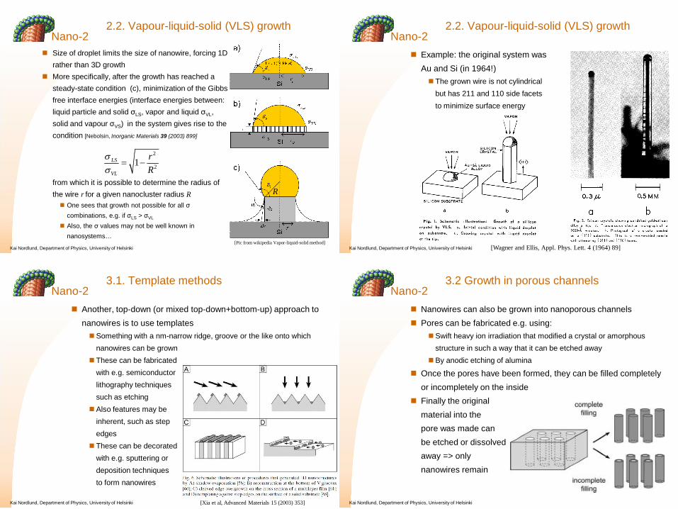
2.1. Spontaneous growth of nanowires
Some materials actually preferentially grow in nanowire formTypically ones which have a layered crystal structureThe layers grow preferentially in some direction, leaving one or two dimensions in a non-growing mode => a wire resultsExamples:
Asbestos(!), chrysoliteLiMo6Se6 (figure)…
[Xia et al, Advanced Materials 15 (2003) 353]
Nano-2
Kai Nordlund, Department of Physics, University of Helsinki
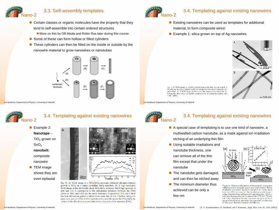
2.1. Spontaneous growth of nanowires
The pure elements Te and Se tend to grow in wires because they have in their trigonal crystal structures straight helical chains
During growth from a solution these drive the growth in a straight direction
[Xia et al, Advanced Materials 15 (2003) 353]
Nano-2
Kai Nordlund, Department of Physics, University of Helsinki
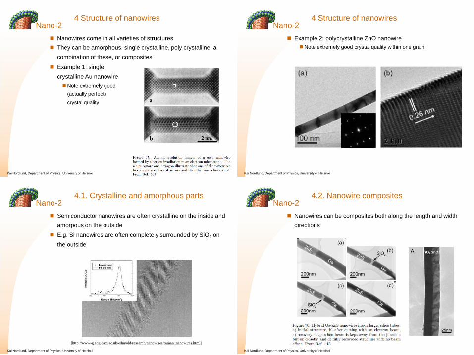
2.2. Vapour-liquid-solid (VLS) growth
The VLS growth method is one of the most used approaches to grow nanowiresContrary to spontaneous growth, it works for a very wide range of materialsKey idea: use a liquid droplet of material B, into which material A is dissolved from the vapour phase (e.g. from CVD or PVD) to form an AB alloyEventually liquid gets supersaturated in AIf then Tmelt,A < Tmelt,AB
(typically in an eutectic alloy),A will start precipitating outof B to form an A nanowireSize of droplet limitsthe size of nanowire, forcing1D rather than 3D growth [http://www.nanowirephotonics.com/research-nanowires.html]
Nano-2
Kai Nordlund, Department of Physics, University of Helsinki
2.2. Vapour-liquid-solid (VLS) growth
Size of droplet limits the size of nanowire, forcing 1D rather than 3D growthMore specifically, after the growth has reached a steady-state condition (c), minimization of the Gibbs free interface energies (interface energies between: liquid particle and solid LS, vapor and liquid VL, solid and vapour VS) in the system gives rise to the condition [Nebolsin, Inorganic Materials 39 (2003) 899]
from which it is possible to determine the radius of the wire r for a given nanocluster radius R
One sees that growth not possible for all combinations, e.g. if LS > VL
Also, the values may not be well known in nanosystems…
2
21LS
VL
rR
[Pic from wikipedia Vapor-liquid-solid method]
R
Nano-2
Kai Nordlund, Department of Physics, University of Helsinki
2.2. Vapour-liquid-solid (VLS) growth
Example: the original system was Au and Si (in 1964!)
The grown wire is not cylindricalbut has 211 and 110 side facetsto minimize surface energy
[Wagner and Ellis, Appl. Phys. Lett. 4 (1964) 89]
Nano-2
Kai Nordlund, Department of Physics, University of Helsinki
3.1. Template methods
Another, top-down (or mixed top-down+bottom-up) approach to nanowires is to use templates
Something with a nm-narrow ridge, groove or the like onto which nanowires can be grownThese can be fabricated with e.g. semiconductor lithography techniques such as etching Also features may be inherent, such as step edgesThese can be decoratedwith e.g. sputtering ordeposition techniquesto form nanowires
[Xia et al, Advanced Materials 15 (2003) 353]
Nano-2
Kai Nordlund, Department of Physics, University of Helsinki
3.2 Growth in porous channels
Nanowires can also be grown into nanoporous channelsPores can be fabricated e.g. using:
Swift heavy ion irradiation that modified a crystal or amorphous structure in such a way that it can be etched awayBy anodic etching of alumina
Once the pores have been formed, they can be filled completely or incompletely on the insideFinally the originalmaterial into thepore was made canbe etched or dissolvedaway => onlynanowires remain
Nano-2
Kai Nordlund, Department of Physics, University of Helsinki
3.3. Self-assembly templates
Certain classes or organic molecules have the property that they tend to self-assemble into certain ordered structures
More on this by Olli Ikkala and Robin Ras later during this course
Some of these can form hollow or filled cylindersThese cylinders can then be filled on the inside or outside by the nanowire material to grow nanowires or nanotubes
Nano-2
Kai Nordlund, Department of Physics, University of Helsinki
3.4. Templating against existing nanowires
Existing nanowires can be used as templates for additional material, to form composite wires!Example 1: silica grown on top of Ag nanowires
Nano-2
Kai Nordlund, Department of Physics, University of Helsinki
3.4. Templating against existing nanowires
Example 2:Nanotape –TiO2 grown on SnO2
nanobelt: composite nanowireTEM image shows they are even epitaxial
Nano-2
Kai Nordlund, Department of Physics, University of Helsinki
3.4. Templating against existing nanowires
A special case of templating is to use one kind of nanowire, a multiwalled carbon nanotube, as a mask against ion irradiation etching of an underlying thin filmUsing suitable irradiations andnanotube thickness, onecan remove all of the thinfilm except that under thenanotubeThe nanotube gets damaged,and can then be etched awayThe minimum diameter thusachieved can be only afew nm
[A. V. Krasheninnikov, K. Nordlund, and J. Keinonen,, Appl. Phys. Lett. 81, 1101 (2002)]
Nano-2
Kai Nordlund, Department of Physics, University of Helsinki
4 Structure of nanowires
Nanowires come in all varieties of structuresThey can be amorphous, single crystalline, poly crystalline, a combination of these, or compositesExample 1: single crystalline Au nanowire
Note extremely good (actually perfect)crystal quality
Nano-2
Kai Nordlund, Department of Physics, University of Helsinki
4 Structure of nanowires
Example 2: polycrystalline ZnO nanowireNote extremely good crystal quality within one grain
Nano-2
Kai Nordlund, Department of Physics, University of Helsinki
4.1. Crystalline and amorphous parts
Semiconductor nanowires are often crystalline on the inside and amorpous on the outsideE.g. Si nanowires are often completely surrounded by SiO2 on the outside
[http://www-g.eng.cam.ac.uk/edm/old/research/nanowires/raman_nanowires.html]
Nano-2
Kai Nordlund, Department of Physics, University of Helsinki
4.2. Nanowire composites
Nanowires can be composites both along the length and width directions
TiO2 SnO2
Nano-2
Kai Nordlund, Department of Physics, University of Helsinki
5. Mechanical properties
Single-crystalline whiskers and nanowires can be atomically perfect
Bulk counterparts always contain some concentration of defects
Hence they can be mechanically stronger than the corresponding bulk material
“Chain is as strong as its weakest point” –but now there are no weak points…
Whiskers have hence for a long time been used as reinforcements of composites
Standard example: SiC whisker reinforced carbon fiber composites
[http://www.tms.org/pubs/journals/JOM/0903/gianola-0903.html]
Cu whiskers
Nano-2
Kai Nordlund, Department of Physics, University of Helsinki
5. Mechanical properties
Since whiskers/nanowires form atomically perfect single crystals, they are also of basic mechanical science interest as a prototype material to observe crystallographic slip
[http://www.tms.org/pubs/journals/JOM/0903/gianola-0903.html]
Nano-2
Kai Nordlund, Department of Physics, University of Helsinki
6. Electrical properties
Transistors with single nanowiresas the current-carrying element have been fabricated Example: InP nanowireswith clear transistor-like characteristics
Nano-2
Kai Nordlund, Department of Physics, University of Helsinki
6. Electrical properties
Even more advanced circuitry consisting of several nanowires have been made
Nano-2
Kai Nordlund, Department of Physics, University of Helsinki
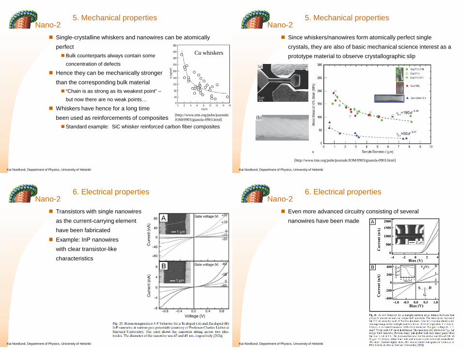
7. Optical properties
As in quantum dots, quantum confinement makes the optical properties of nanowires interestingOn the other hand, if the nanowires are free-standing, a suitable combination of the refractive indices of the nanowire and surrounding material (e.g. air) can make them act as waveguides for lightFinally, in some cases of even more suitable combinations of the refractive indices, the ends of the nanowire can act as mirrorsThus a single nanowire may act as a lasing elementThis has been demonstrated for ZnO nanowires on sapphire surrounded by air
Nano-2
Kai Nordlund, Department of Physics, University of Helsinki
7. Optical properties
Example
Nano-2
Kai Nordlund, Department of Physics, University of Helsinki
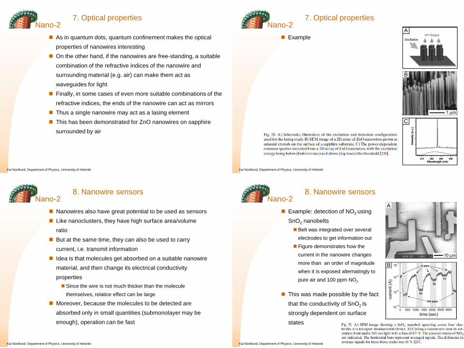
8. Nanowire sensors
Nanowires also have great potential to be used as sensorsLike nanoclusters, they have high surface area/volume ratioBut at the same time, they can also be used to carry current, i.e. transmit informationIdea is that molecules get absorbed on a suitable nanowire material, and then change its electrical conductivity properties
Since the wire is not much thicker than the molecule themselves, relatice effect can be large
Moreover, because the molecules to be detected are absorbed only in small quantities (submonolayer may be enough), operation can be fast
Nano-2
Kai Nordlund, Department of Physics, University of Helsinki
8. Nanowire sensors
Example: detection of NO2 using SnO2 nanobelts
Belt was integrated over several electrodes to get information outFigure demonstrates how the current in the nanowire changes more than an order of magnitude when it is exposed alternatingly to pure air and 100 ppm NO2
This was made possible by the fact that the conductivity of SnO2 is strongly dependent on surface states

Nano-2
Kai Nordlund, Department of Physics, University of Helsinki
9. Example: generating electricity from ZnO
A really exciting possible application stems from the observation that ZnO nanowires are piezoelectric, i.e. a mechanical strain can generate electricity in themThis effect was shown [Wang et al, Science 312(2006) 242] to enable electricity generation directly from mechanical force with efficiencies of 17 – 30%
Nano-2
Kai Nordlund, Department of Physics, University of Helsinki
9. Example: generating electricity from ZnO
The reason this is exciting is that such nanowires could be inserted into really small devices, such as portable electronics, implantable medical devices or even the heels of a shoe to generate electrical power for other nano- and microscale devices
No external power source needed?