Embed Size (px)
Citation preview
Conquering SMT Stencil Printing Challenges with Today’s Miniature Components
Is Electroform Technology the Right Solution?
By Robert F. Dervaes, V.P. Technology and Engineering, Fine Line Stencil, Inc., Jeff Poulos,
V.P. of Manufacturing and Sales, Alternative Solutions, Inc., and Scott Williams,
Product/Account Manager, Ed Fagan, Inc.
The technological advancement of component and PCB technology from through-hole to surface
mount (SMT) is a major factor in the miniaturization of today’s electronics. Smaller and smaller
component sizes and more densely packed PCBs lead to more powerful designs in much smaller
product packages. With advancement, however, comes a new set of challenges in building these
smaller, more complex assemblies. This is the challenge original equipment manufacturers
(OEM) and contract manufacturers (CM) face today.
One of the challenges facing OEMs and CMs in building assemblies with miniature components
is the stencil printing process. Many of today’s designs incorporate a mix of miniature and much
larger components. Manufacturing engineers are faced with the dilemma of choosing a thinner
stencil foil to ensure solder paste release for the miniature components or a thicker foil to ensure
sufficient solder volume for the larger components. With a standard laser-cut stencil using 300
series stainless steel, one would have to make that difficult choice. An electroformed stencil
gives more options in balancing release for miniature components and volume for larger ones
due to its ability to successfully print smaller components without reducing the foil thickness.
However, many have difficulty justifying the 3X-4X cost increase and added schedule delay for
an electroformed stencil, especially with more and more companies moving to a low-volume,
high-mix array of jobs. Faced with these two options, is electroformed technology the right
solution or have technological advancements allowed new developments in stencil technology?
This article discusses new developments in stencil laser and material technology and shows how
these advancements, when combined, provide comparable and cost-effective alternatives to
traditional electroformed stencils. The results are improved yields, cycle time reductions, and
significant cost savings.
Brief History of Stencil Technologies
Before stencil lasers were developed, the only manufacturing methods for producing solder paste
stencils were silk screening and chemical etching. The etching process was time consuming and
hazardous due to the powerful chemicals used to etch the metal. There also were limitations as to
how small a stencil aperture could be effectively produced during the etching process.
Chemically etched stencils typically were limited to component pitches no smaller than 0.025"
and registration of the stencil apertures to the SMT pads was not precise enough as component
sizes decreased. These limitations would not allow chemical etching to keep pace with the rapid
advancements in component and PCB design.
In the early 1990s, lasers started being used to produce solder paste stencils. This new
technology was a major improvement over traditional silk screen and chemical etching in
producing stencils quicker, cheaper, and with much smaller aperture sizes. The motion systems
on the laser systems also provided a much higher positional accuracy for the stencil apertures,
leading to much better alignment between the stencil and PCB. With these significant
improvements, component pitches down to 0.016" could easily be cut.
While these laser systems are capable of producing high-quality solder paste stencils for the
majority of assemblies, advancements in component and PCB design continued. With the
introduction of components like “micro BGA (µBGA),” “quad flat no-lead (QFN),” and 0201s,
laser-cut stencils struggled to produce acceptable solder paste release for these very small
apertures without a reduction in the thickness of the stencil foil. This was not always an
acceptable solution as the larger components would have insufficient solder volume. Enter
electroformed technology. Electroformed stencils are produced by electroplating Nickel on top
of a Stainless Steel substrate under various specialized and challenging conditions. The plated
Nickel film is later removed from the Stainless Steel substrate resulting in the Nickel foil that is
the electroformed stencil. This manufacturing process produces an exceptionally smooth stencil
aperture wall compared to chemically etched and traditional laser-cut stencils. The smoothness
of the aperture wall is a vital component of a high performance stencil allowing printing of
smaller apertures without reducing the foil thickness.
For many years, electroformed stencils have been the premier solution for these new, challenging
assemblies. However, the assembly industry as a whole is being driven to turn product faster and
cheaper. Electroformed stencil prices typically are 3X-4X higher than traditional laser-cut
stencils and it takes longer to produce an electroformed stencil. In most cases, the turn time is 3
to 4 days and this technology is limited to only a few shops that have the knowledge and
expertise in plating very thin Nickel foils. Many OEMs and CMs need stencils produced and
shipped the day the order is placed in order to meet their schedule. The higher cost and longer
lead-time of electroformed stencils make it more difficult to meet the schedule and cost demands
of today’s assemblies. How does one determine if a traditional laser-cut or electroformed stencil
is required?
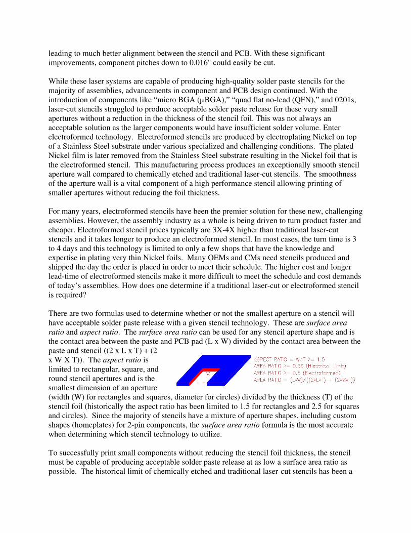
There are two formulas used to determine whether or not the smallest aperture on a stencil will
have acceptable solder paste release with a given stencil technology. These are surface area
ratio and aspect ratio. The surface area ratio can be used for any stencil aperture shape and is
the contact area between the paste and PCB pad (L x W) divided by the contact area between the
paste and stencil ((2 x L x T) + (2
x W X T)). The aspect ratio is
limited to rectangular, square, and
round stencil apertures and is the
smallest dimension of an aperture
(width (W) for rectangles and squares, diameter for circles) divided by the thickness (T) of the
stencil foil (historically the aspect ratio has been limited to 1.5 for rectangles and 2.5 for squares
and circles). Since the majority of stencils have a mixture of aperture shapes, including custom
shapes (homeplates) for 2-pin components, the surface area ratio formula is the most accurate
when determining which stencil technology to utilize.
To successfully print small components without reducing the stencil foil thickness, the stencil
must be capable of producing acceptable solder paste release at as low a surface area ratio as
possible. The historical limit of chemically etched and traditional laser-cut stencils has been a
surface area ratio of 0.66. In the case of electroformed stencils, the limit has been improved to
0.5. The lower surface area ratio limit of electroformed stencils is the reason for selecting this
technology when facing challenging assemblies.
With all of the advancements in component and PCB design, has advancement in the stencil
industry remained stagnant or has technological improvement benefited this industry as well? Is
the stencil industry now in a better position to provide solutions for printing miniature
components while meeting customers’ tighter delivery and cost requirements?
New Developments in Stencil Laser Technology
Stencil laser technology has seen continuous advancement over the past 10 years. The majority
of advancement has been in linear motor technology, leading to improvements in the cutting
speed of stencil lasers. Until recently, the source of the laser beam has remained the same with
reliance on lamp pumped technology. The lamp pumped technology is comprised of flash lamps,
YAG rods, mirrors, and focal lenses. With this technology, the smallest diameter laser beam
possible was approximately 40 µm. While this diameter beam is fine for the majority of stencil
designs, the energy density with a 40 µm beam diameter is not high enough to produce the
smoothest aperture walls when cutting stencil apertures for miniature components.
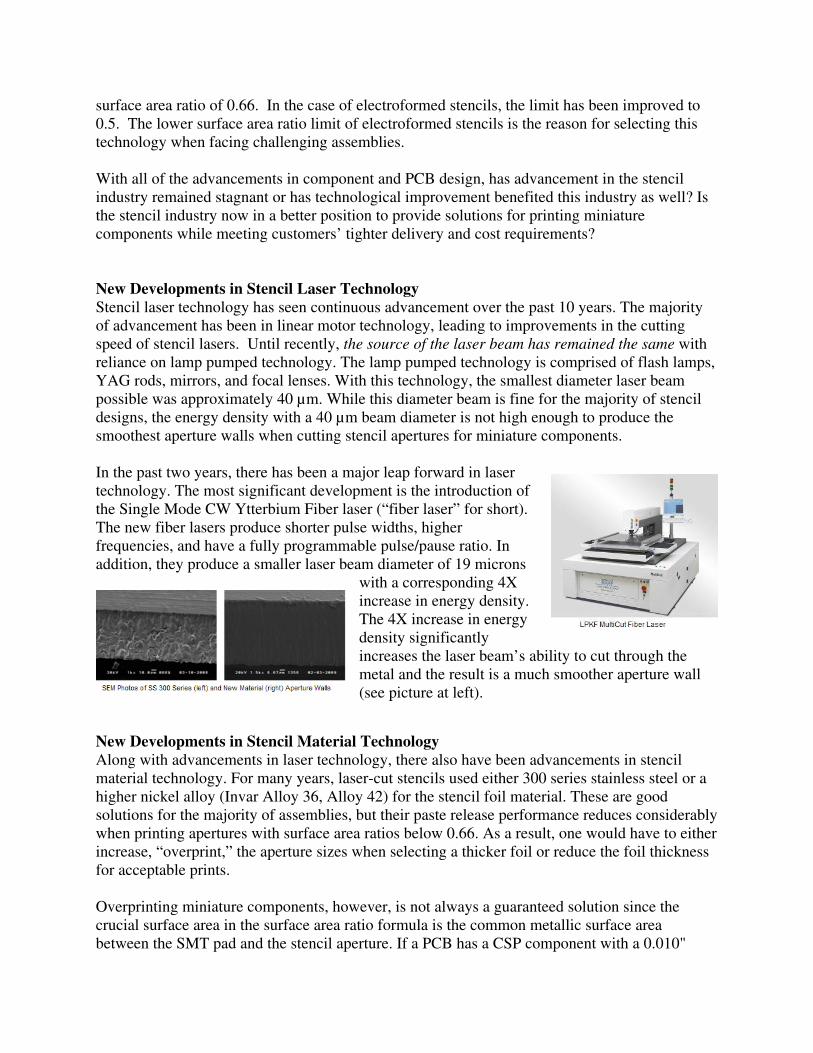
In the past two years, there has been a major leap forward in laser
technology. The most significant development is the introduction of
the Single Mode CW Ytterbium Fiber laser (“fiber laser” for short).
The new fiber lasers produce shorter pulse widths, higher
frequencies, and have a fully programmable pulse/pause ratio. In
addition, they produce a smaller laser beam diameter of 19 microns
with a corresponding 4X
increase in energy density.
The 4X increase in energy
density significantly
increases the laser beam’s ability to cut through the
metal and the result is a much smoother aperture wall
(see picture at left).
New Developments in Stencil Material Technology
Along with advancements in laser technology, there also have been advancements in stencil
material technology. For many years, laser-cut stencils used either 300 series stainless steel or a
higher nickel alloy (Invar Alloy 36, Alloy 42) for the stencil foil material. These are good
solutions for the majority of assemblies, but their paste release performance reduces considerably
when printing apertures with surface area ratios below 0.66. As a result, one would have to either
increase, “overprint,” the aperture sizes when selecting a thicker foil or reduce the foil thickness
for acceptable prints.
Overprinting miniature components, however, is not always a guaranteed solution since the
crucial surface area in the surface area ratio formula is the common metallic surface area
between the SMT pad and the stencil aperture. If a PCB has a CSP component with a 0.010"
diameter pad and the stencil overprints with a 0.012" diameter aperture, the common metallic
surface is still limited to the 0.010" diameter of the SMT pad. The additional paste beyond the
0.010" limit of the SMT pad is not in contact with the metallic surface and, therefore, does not
contribute to pulling the paste from the stencil.
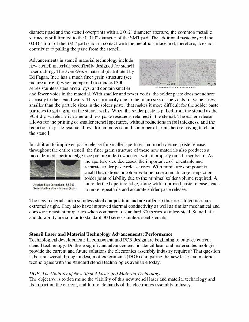
Advancements in stencil material technology include
new stencil materials specifically designed for stencil
laser-cutting. The Fine Grain material (distributed by
Ed Fagan, Inc.) has a much finer grain structure (see
picture at right) when compared to standard 300
series stainless steel and alloys, and contain smaller
and fewer voids in the material. With smaller and fewer voids, the solder paste does not adhere
as easily to the stencil walls. This is primarily due to the micro size of the voids (in some cases
smaller than the particle sizes in the solder paste) that makes it more difficult for the solder paste
particles to get a grip on the stencil walls. When the solder paste is pulled from the stencil as the
PCB drops, release is easier and less paste residue is retained in the stencil. The easier release
allows for the printing of smaller stencil apertures, without reductions in foil thickness, and the
reduction in paste residue allows for an increase in the number of prints before having to clean
the stencil.
In addition to improved paste release for smaller apertures and much cleaner paste release
throughout the entire stencil, the finer grain structure of these new materials also produces a
more defined aperture edge (see picture at left) when cut with a properly tuned laser beam. As
the aperture size decreases, the importance of repeatable and
accurate solder paste release rises. With miniature components,
small fluctuations in solder volume have a much larger impact on
solder joint reliability due to the minimal solder volume required. A
more defined aperture edge, along with improved paste release, leads
to more repeatable and accurate solder paste release.
The new materials are a stainless steel composition and are rolled so thickness tolerances are
extremely tight. They also have improved thermal conductivity as well as similar mechanical and
corrosion resistant properties when compared to standard 300 series stainless steel. Stencil life
and durability are similar to standard 300 series stainless steel stencils.
Stencil Laser and Material Technology Advancements: Performance
Technological developments in component and PCB design are beginning to outpace current
stencil technology. Do these significant advancements in stencil laser and material technologies
provide the current and future solutions the electronics assembly industry requires? That question
is best answered through a design of experiments (DOE) comparing the new laser and material
technologies with the standard stencil technologies available today.
DOE: The Viability of New Stencil Laser and Material Technology
The objective is to determine the viability of this new stencil laser and material technology and
its impact on the current, and future, demands of the electronics assembly industry.
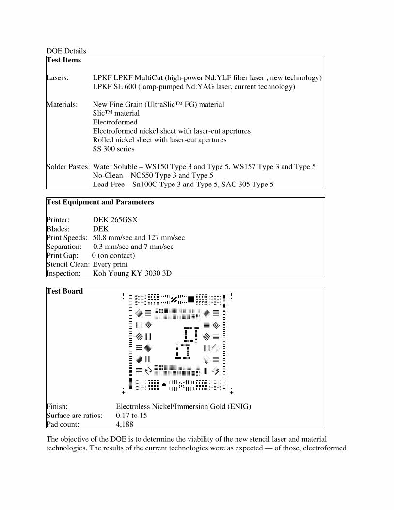
DOE Details
Test Items
Lasers: LPKF LPKF MultiCut (high-power Nd:YLF fiber laser , new technology)
LPKF SL 600 (lamp-pumped Nd:YAG laser, current technology)
Materials: New Fine Grain (UltraSlic™ FG) material
Slic™ material
Electroformed
Electroformed nickel sheet with laser-cut apertures
Rolled nickel sheet with laser-cut apertures
SS 300 series
Solder Pastes: Water Soluble – WS150 Type 3 and Type 5, WS157 Type 3 and Type 5
No-Clean – NC650 Type 3 and Type 5
Lead-Free – Sn100C Type 3 and Type 5, SAC 305 Type 5
Test Equipment and Parameters
Printer: DEK 265GSX
Blades: DEK
Print Speeds: 50.8 mm/sec and 127 mm/sec
Separation: 0.3 mm/sec and 7 mm/sec
Print Gap: 0 (on contact)
Stencil Clean: Every print
Inspection: Koh Young KY-3030 3D
Test Board
Finish: Electroless Nickel/Immersion Gold (ENIG)
Surface are ratios: 0.17 to 15
Pad count: 4,188
The objective of the DOE is to determine the viability of the new stencil laser and material
technologies. The results of the current technologies were as expected — of those, electroformed
had the best solder paste release. How did the new stencil laser and material technology compare
to current stencil technologies?
New Fine Grain Performance
The surface area ratio limit for electroformed technology is 0.5. While a significant improvement
over standard laser-cut stencils, materials that offer improved performance at area ratios of 0.5,
and below are going to be a requirement as component and PCB technology continues to
advance.
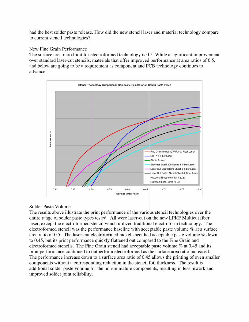
Stencil Technology Comparison: Composite Results for all Solder Paste Types
0.40 0.45 0.50 0.55 0.60 0.65 0.70 0.75 0.80
Surface Area Ratio
Paste
Vo
lum
e %
Fine Grain (UltraSlic™ FG) & Fiber Laser
Slic™ & Fiber Laser
Electroformed
Stainless Steel 300 Series & Fiber Laser
Laser-Cut Electroform Sheet & Fiber Laser
Laser-Cut Rolled Nickel Sheet & Fiber Laser
Historical Electroform Limit (0.5)
Historical Laser Limit (0.66)
Solder Paste Volume
The results above illustrate the print performance of the various stencil technologies over the
entire range of solder paste types tested. All were laser-cut on the new LPKF Multicut fiber
laser, except the electroformed stencil which utilized traditional electroform technology. The
electroformed stencil was the performance baseline with acceptable paste volume % at a surface
area ratio of 0.5. The laser-cut electroformed nickel sheet had acceptable paste volume % down
to 0.45, but its print performance quickly flattened out compared to the Fine Grain and
electroformed stencils. The Fine Grain stencil had acceptable paste volume % at 0.45 and its
print performance continued to outperform electroformed as the surface area ratio increased.
The performance increase down to a surface area ratio of 0.45 allows the printing of even smaller
components without a corresponding reduction in the stencil foil thickness. The result is
additional solder paste volume for the non-miniature components, resulting in less rework and
improved solder joint reliability.
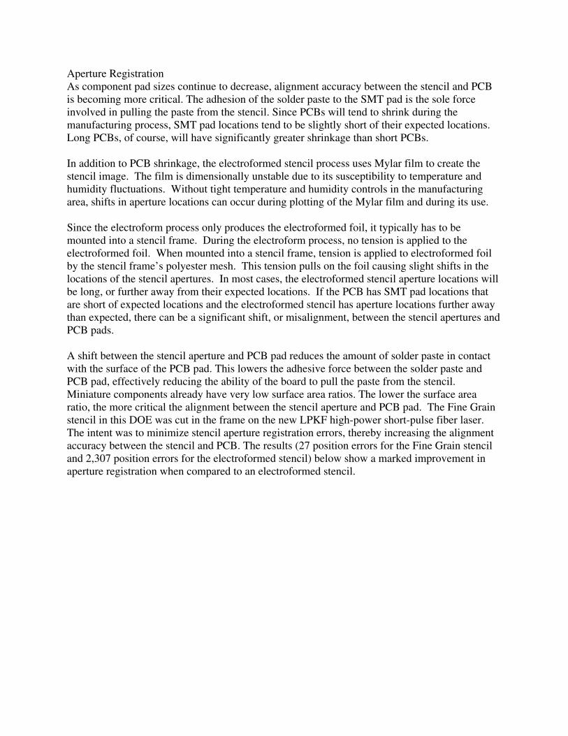
Aperture Registration
As component pad sizes continue to decrease, alignment accuracy between the stencil and PCB
is becoming more critical. The adhesion of the solder paste to the SMT pad is the sole force
involved in pulling the paste from the stencil. Since PCBs will tend to shrink during the
manufacturing process, SMT pad locations tend to be slightly short of their expected locations.
Long PCBs, of course, will have significantly greater shrinkage than short PCBs.
In addition to PCB shrinkage, the electroformed stencil process uses Mylar film to create the
stencil image. The film is dimensionally unstable due to its susceptibility to temperature and
humidity fluctuations. Without tight temperature and humidity controls in the manufacturing
area, shifts in aperture locations can occur during plotting of the Mylar film and during its use.
Since the electroform process only produces the electroformed foil, it typically has to be
mounted into a stencil frame. During the electroform process, no tension is applied to the
electroformed foil. When mounted into a stencil frame, tension is applied to electroformed foil
by the stencil frame’s polyester mesh. This tension pulls on the foil causing slight shifts in the
locations of the stencil apertures. In most cases, the electroformed stencil aperture locations will
be long, or further away from their expected locations. If the PCB has SMT pad locations that
are short of expected locations and the electroformed stencil has aperture locations further away
than expected, there can be a significant shift, or misalignment, between the stencil apertures and
PCB pads.
A shift between the stencil aperture and PCB pad reduces the amount of solder paste in contact
with the surface of the PCB pad. This lowers the adhesive force between the solder paste and
PCB pad, effectively reducing the ability of the board to pull the paste from the stencil.
Miniature components already have very low surface area ratios. The lower the surface area
ratio, the more critical the alignment between the stencil aperture and PCB pad. The Fine Grain
stencil in this DOE was cut in the frame on the new LPKF high-power short-pulse fiber laser.
The intent was to minimize stencil aperture registration errors, thereby increasing the alignment
accuracy between the stencil and PCB. The results (27 position errors for the Fine Grain stencil
and 2,307 position errors for the electroformed stencil) below show a marked improvement in
aperture registration when compared to an electroformed stencil.
Electroformed (left) and Fine Grain (right) Stencil Aperture Registration Accuracy
2,307 position errors with the electroformed stencil and 27 with the Fine Grain stencil
Conclusion
As advancements continue in component and PCB technologies, will the stencil technology of
today provide current and future solutions to the challenging assembly issues faced by OEMs
and CMs? Is electroformed technology the right solution or have new developments in stencil
laser and material technologies caught up with and surpassed the electroformed technology of
today?
The answer to these important questions is in our view an unequivocal “yes.” Stencil laser and
material technologies have advanced to the point where laser-cut stencil performance is beyond
that of current electroformed technology. Using the new LPKF high-power short-pulse fiber
laser technology and the new Fine Grain material, stencil performance is significantly improved
over electroformed, especially when printing miniature components. Improvements in stencil
laser and material technologies have lead to significant improvements in solder paste release
down to a surface area ratio of 0.45 as well as improved aperture registration accuracy. These
improvements are critical to meeting future requirements when printing miniature components
like 01005s. The technology summary is as follows:
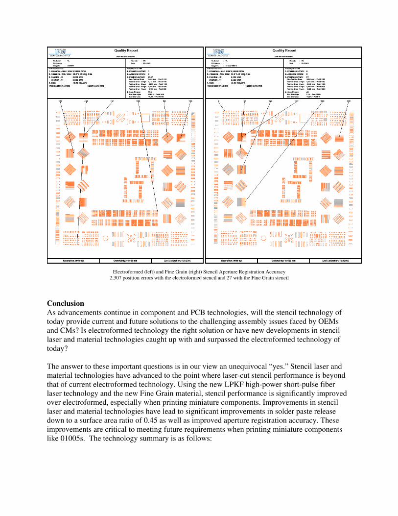
Stencil Technology Summary
Technology Minimum
Surface Area
Ratio
Cost Material Aperture
Registration
Accuracy
Chemical Etch 0.66 Low SS, Alloy Moderate
Traditional
Laser-Cut
0.66 Low SS, Alloy Very High
Traditional
Laser-Cut
0.55 Low Slic™ Very High
Electroformed 0.5 High Electroformed
Nickel
High
Advanced Laser-
Cut
0.45 Medium Fine Grain Very High
At a cost savings of 30-50 percent compared to electroformed, the ability to produce multi-
thickness (step) stencils, and the option of same day turn times, Fine Grain stencils, cut with the
new fiber lasers, are a marked improvement compared to the high-performance stencil solutions
available today. OEMs and CMs can get the performance they need while reducing costs and
meeting critical delivery schedules. The new stencil laser and material technologies available
today give stencil manufacturers the tools and materials needed to supply an ever-changing
industry for many years to come.
ACKNOWLEDGEMENT
The authors would like to thank Stephan Schmidt and Sebastian Gerberding of LPKF Laser
Electronics (www.lpkfusa.com) for their contribution to this article.