Embed Size (px)
Citation preview
Quarter 3 • 2012 12555 SW Leveton Drive • Tualatin Oregon 97062 • USA • www.lpkfusa.com
4 Quarter 3 • 2012
GENERAL INQUIRIES
Phone numbers:1-800-345-LPKF1-503-454-4200Fax: 1-503-682-7151
Mailing address:LPKF Laser & ElectronicsNorth America12555 SW Leveton Dr.Tualatin, OR 97062United States
SUPPORT
Technical SupportPlotter [email protected]
Technical SupportLaser [email protected]
SALES
System [email protected]
Materials & Tools [email protected]
www.lpkfusa.com
Ashley OakesASHLEY OAKES — Marketing Coordinator
Dear valued customer,As summer makes its final encore, we take a look back at all the exciting things that have happened at
LPKF. With a little something for everyone, Quarter three’s newsletter introduces the new MicroLine 6000 P,
LPKF’s Laser Plastic Welding group on LinkedIn, and an interview with Senior Sales Associate Rory Grondin
discussing the differences between a milling machine and a laser etching system. The newsletter also
includes a link to LPKF’s recent SMT Stencil webinar and white paper as well as a new recurring
column that examines a different ProtoMat feature each issue. I sincerely hope that there is something
of interest to each reader and as always, I welcome any questions and/or feedback.
S-Series Spotlight:The FiducialRecognition Camera
It is estimated that 60-75% of all boardassembly problems stem from solder pasteprinting. Therefore it is important for thosein the SMT industry to understand howmanufacturing methods can affect solderpaste application during the printing process.
The white paper “Solder Paste Depositsand the Precision of Aperture Sizes” byAhne Oosterhof, Eastwood Consulting, andStephan Schmidt, LPKF Laser & ElectronicsNorth America, explores the solder pastedispensing process and how different manufacturing methods affect aperture sizes.Originally presented at IPC APEX Expo 2012, the white paper can be accessed at:http://www.lpkfusa.com/SMTStencil/whitepapers/index.html.
In addition to the white paper, LPKF recently hosted the webinar “How StencilManufacturing Methods Impact Precision and Accuracy.” This webinar examinesstencil positional accuracy as a function of the manufacturing process and discussesparameters that affect the accuracy and location of solder paste dispensing. Todownload a recorded version of the webinar, visit:http://www.lpkfusa.com/SMTStencil/webinars/How-Stencil-Manufacturing-Methods-Impact-Precision-and-Accuracy.html.
Between both the paper and webinar, there is an opportunity to understand dimensionalaccuracy across the full stencil as well as the accuracy of individual apertures, andhow both of these factors contribute to quality and yield.
Fall/Winter 2012 Trade Show Schedule
Show
PCB West
SMTA International
EPTECH Ottawa
MILCOM
BIOMEDevice
Location
Santa Clara, CA
Orlando, FL
Ottawa, Canada
Orlando, FL
San Jose, CA
Dates
Sept. 26
Oct. 16-17
Oct. 25
Oct. 30-Nov. 1
Dec. 4-5
Booth
319
417
TBD
130
940
LPKF Announces New SMT StencilWhite Paper & Webinar
Considerably improving the process ofin-house PCB prototyping, the fiducialrecognition camera automatically locatesand registers fiducial markers for boardalignment. It also eliminates the needfor set pins for front to back alignmentand aids multilayer applications,ensuring each layer is precisely alignedwhile adjusting for any stretch duringthe heated lamination process.
As an added feature, the fiducial camerameasures the cut widths of V-shapedtools to verify that depth settings arecorrect and design specifications aremet, improving the automatic toolchange process. Originally introducedwith the ProtoMat H100 in 2003, thecamera is now standard on the ProtoMatS63 and S103, and is an optionalfeature on the entry-level ProtoMat S43.To learn more about the fiducialrecognition camera and its capabilities,check out the LPKF YouTube video:http://www.youtube.com/watch?v=-tVZ-sdxG2o
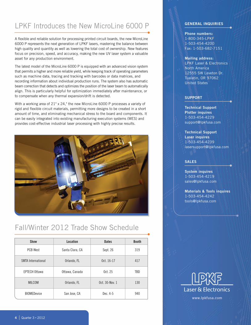
A flexible and reliable solution for processing printed circuit boards, the new MicroLine6000 P represents the next generation of LPKF lasers, mastering the balance betweenhigh quality and quantity as well as lowering the total cost of ownership. New featuresfocus on precision, speed, and accuracy, making the new UV laser system a valuableasset for any production environment.
The latest model of the MicroLine 6000 P is equipped with an advanced vision systemthat permits a higher and more reliable yield, while keeping track of operating parameterssuch as machine data, tracing and tracking with barcodes or data matrices, andrecording information about individual production runs. The system also has automaticbeam correction that detects and optimizes the position of the laser beam to automaticallyalign. This is particularly helpful for optimization immediately after maintenance, orto compensate when any thermal expansion/drift is detected.
With a working area of 21" x 24," the new MicroLine 6000 P processes a variety ofrigid and flexible circuit materials, permitting more designs to be created in a shortamount of time, and eliminating mechanical stress to the board and components. Itcan be easily integrated into existing manufacturing execution systems (MES) andprovides cost-effective industrial laser processing with highly precise results.
LPKF Introduces the New MicroLine 6000 P
Dispensing solder pastewith the ProtoPlace S
Helpful hints to keep your machineoperational and protect your asset.
MaintenanceCORNER
PCB prototyping is a universal step in the electrical engineering process, and LPKFhas several in-house prototyping options including mechanical milling and laser etchingof PCBs. But how does a company decide which system is the best fit? Dependingon project requirements, there are several factors to take into consideration such asspeed, accuracy, and material. What follows is an interview with Rory Grondin, SeniorSales Associate, LPKF Laser & Electronics North America, discussing the differencesbetween the LPKF ProtoMat milling machines and the ProtoLaser laser etching systems.
Q: What key factors help customers decide whether a milling machine or laser systemis the best fit?
R: The desired application will decide which system is best for a company. Thisincludes design requirements, material, and the volume of prototypes or small batchproduction boards needed.
Q: What are the main differences between a laser system and a milling machine?
R: Speed, materials and space/trace capabilities. The laser processing speeds aremuch faster than mechanical milling and can process a wider range of materialincluding alumina and fired ceramics. The laser systems also allows traces as smallas 50µm and spacing as small as 25µm while the milling machine permits 4 mil(100µm) traces and 4 mil spacing.
Q: For customers who own a milling machine, when should they consider bringinga laser system in-house?
R: The ProtoLaser Systems can be an invaluable tool when the quantity of prototypeboards needed is more than can be completed on the PCB milling system in a desiredtime frame. The ProtoLaser S or U3 laser etching capabilities can dramatically speedup this process and is approximately seven times faster than traditional surfacemechanical milling.
Also, if RF/microwave designs are the main focus; the ProtoLaser S or U3 laseretching improves edge quality and essentially eliminates any effect on the substratesurface. Completed boards match the simulation software almost perfectly and smallbatch production can be completed on the same machine.
If fired ceramics/alumina processing is needed, laser etching would be the bestalternative to chemical etching. The ProtoLaser has proven more consistent on avariety of materials and allows for smaller traces and spacing.
Q: When should a company consider owning a milling machine and a laser system?
R: The most advanced research and development labs include both an LPKFmechanical PCB milling system and a ProtoLaser model. Various capabilities areoffered with each system and one solution may be faster than the other.
For example, drilling through-holes in FR4 substrate can be performed with a lasersystem but is completed much faster on the mechanical milling system on thickermaterials. The LPKF ProtoMat S63 and S103 systems also allow for depth millingusing a stepper motor control z-drive; pockets can be created in aluminum, brass,copper and even plastics to a set depth. The laser systems surpasses PCB milling withsurface metallization removal both in precision and time required; the laser systemsalso permits smaller drill holes depending on the material thickness and type.
Q: Is the price of a laser system justifiable?
R: The initial investment of the ProtoLaser models can be easily justified if theoutsourcing costs are high, which is common with alumina and PTFE based/highfrequency substrate materials. The laser systems also save money by eliminatingtooling requirements, reducing time to market, and permitting a wider range ofapplications for R&D to be completed.
Mechanical Milling or Laser Etching:Which is the Right Choice?
How to Plate Through-holeswith LPKF Equipment
2 Quarter 3 • 2012
Did you know ?
Link:
http://www.lpkfusa.com/store/
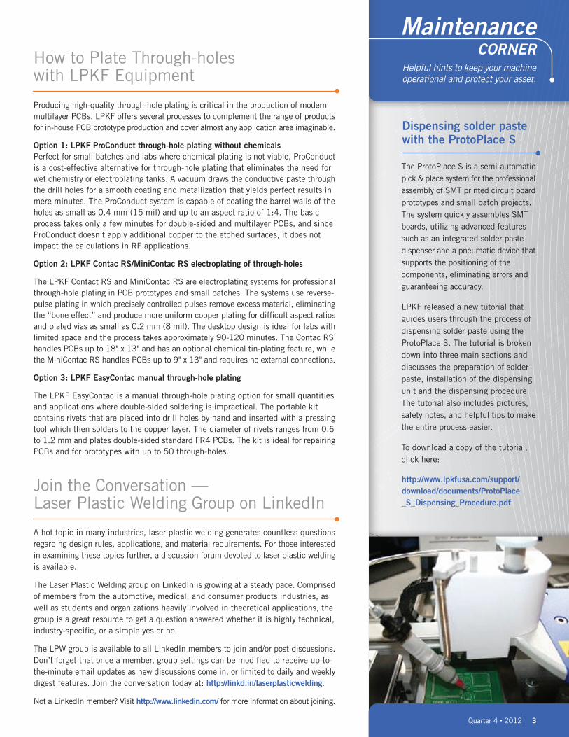
The ProtoPlace S is a semi-automaticpick & place system for the professionalassembly of SMT printed circuit boardprototypes and small batch projects.The system quickly assembles SMTboards, utilizing advanced featuressuch as an integrated solder pastedispenser and a pneumatic device thatsupports the positioning of thecomponents, eliminating errors andguaranteeing accuracy.
LPKF released a new tutorial thatguides users through the process ofdispensing solder paste using theProtoPlace S. The tutorial is brokendown into three main sections anddiscusses the preparation of solderpaste, installation of the dispensingunit and the dispensing procedure.The tutorial also includes pictures,safety notes, and helpful tips to makethe entire process easier.
To download a copy of the tutorial,click here:
3Quarter 4 • 2012
Producing high-quality through-hole plating is critical in the production of modernmultilayer PCBs. LPKF offers several processes to complement the range of productsfor in-house PCB prototype production and cover almost any application area imaginable.
Option 1: LPKF ProConduct through-hole plating without chemicalsPerfect for small batches and labs where chemical plating is not viable, ProConductis a cost-effective alternative for through-hole plating that eliminates the need forwet chemistry or electroplating tanks. A vacuum draws the conductive paste throughthe drill holes for a smooth coating and metallization that yields perfect results inmere minutes. The ProConduct system is capable of coating the barrel walls of theholes as small as 0.4 mm (15 mil) and up to an aspect ratio of 1:4. The basicprocess takes only a few minutes for double-sided and multilayer PCBs, and sinceProConduct doesn’t apply additional copper to the etched surfaces, it does notimpact the calculations in RF applications.
Option 2: LPKF Contac RS/MiniContac RS electroplating of through-holes
The LPKF Contact RS and MiniContac RS are electroplating systems for professionalthrough-hole plating in PCB prototypes and small batches. The systems use reverse-pulse plating in which precisely controlled pulses remove excess material, eliminatingthe “bone effect” and produce more uniform copper plating for difficult aspect ratiosand plated vias as small as 0.2 mm (8 mil). The desktop design is ideal for labs withlimited space and the process takes approximately 90-120 minutes. The Contac RShandles PCBs up to 18" x 13" and has an optional chemical tin-plating feature, whilethe MiniContac RS handles PCBs up to 9" x 13" and requires no external connections.
Option 3: LPKF EasyContac manual through-hole plating
The LPKF EasyContac is a manual through-hole plating option for small quantitiesand applications where double-sided soldering is impractical. The portable kitcontains rivets that are placed into drill holes by hand and inserted with a pressingtool which then solders to the copper layer. The diameter of rivets ranges from 0.6to 1.2 mm and plates double-sided standard FR4 PCBs. The kit is ideal for repairingPCBs and for prototypes with up to 50 through-holes.
Join the Conversation —Laser Plastic Welding Group on LinkedIn
A hot topic in many industries, laser plastic welding generates countless questionsregarding design rules, applications, and material requirements. For those interestedin examining these topics further, a discussion forum devoted to laser plastic weldingis available.
The Laser Plastic Welding group on LinkedIn is growing at a steady pace. Comprisedof members from the automotive, medical, and consumer products industries, aswell as students and organizations heavily involved in theoretical applications, thegroup is a great resource to get a question answered whether it is highly technical,industry-specific, or a simple yes or no.
The LPW group is available to all LinkedIn members to join and/or post discussions.Don’t forget that once a member, group settings can be modified to receive up-to-the-minute email updates as new discussions come in, or limited to daily and weeklydigest features. Join the conversation today at: http://linkd.in/laserplasticwelding.
Not a LinkedIn member? Visit http://www.linkedin.com/ for more information about joining.
http://www.lpkfusa.com/support/download/documents/ProtoPlace_S_Dispensing_Procedure.pdf
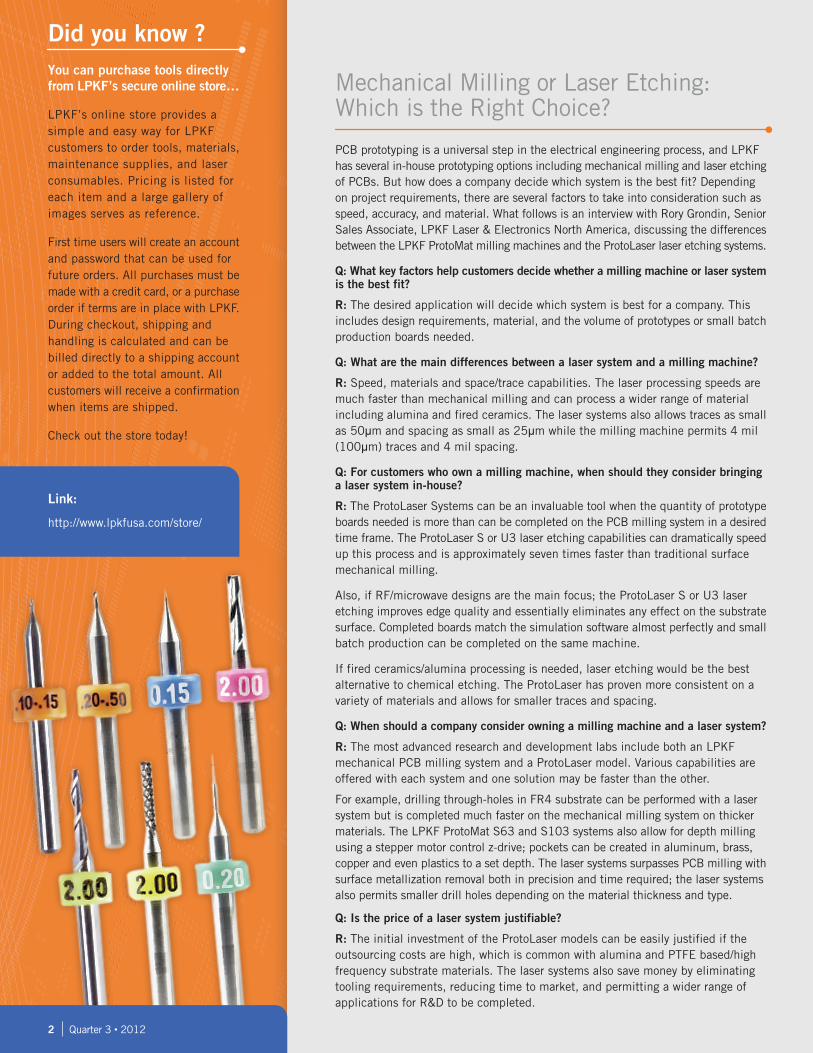
LPKF’s online store provides asimple and easy way for LPKFcustomers to order tools, materials,maintenance supplies, and laserconsumables. Pricing is listed foreach item and a large gallery ofimages serves as reference.
First time users will create an accountand password that can be used forfuture orders. All purchases must bemade with a credit card, or a purchaseorder if terms are in place with LPKF.During checkout, shipping andhandling is calculated and can bebilled directly to a shipping accountor added to the total amount. Allcustomers will receive a confirmationwhen items are shipped.
Check out the store today!
Dispensing solder pastewith the ProtoPlace S
Helpful hints to keep your machineoperational and protect your asset.
MaintenanceCORNER
PCB prototyping is a universal step in the electrical engineering process, and LPKFhas several in-house prototyping options including mechanical milling and laser etchingof PCBs. But how does a company decide which system is the best fit? Dependingon project requirements, there are several factors to take into consideration such asspeed, accuracy, and material. What follows is an interview with Rory Grondin, SeniorSales Associate, LPKF Laser & Electronics North America, discussing the differencesbetween the LPKF ProtoMat milling machines and the ProtoLaser laser etching systems.
Q: What key factors help customers decide whether a milling machine or laser systemis the best fit?
R: The desired application will decide which system is best for a company. Thisincludes design requirements, material, and the volume of prototypes or small batchproduction boards needed.
Q: What are the main differences between a laser system and a milling machine?
R: Speed, materials and space/trace capabilities. The laser processing speeds aremuch faster than mechanical milling and can process a wider range of materialincluding alumina and fired ceramics. The laser systems also allows traces as smallas 50µm and spacing as small as 25µm while the milling machine permits 4 mil(100µm) traces and 4 mil spacing.
Q: For customers who own a milling machine, when should they consider bringinga laser system in-house?
R: The ProtoLaser Systems can be an invaluable tool when the quantity of prototypeboards needed is more than can be completed on the PCB milling system in a desiredtime frame. The ProtoLaser S or U3 laser etching capabilities can dramatically speedup this process and is approximately seven times faster than traditional surfacemechanical milling.
Also, if RF/microwave designs are the main focus; the ProtoLaser S or U3 laseretching improves edge quality and essentially eliminates any effect on the substratesurface. Completed boards match the simulation software almost perfectly and smallbatch production can be completed on the same machine.
If fired ceramics/alumina processing is needed, laser etching would be the bestalternative to chemical etching. The ProtoLaser has proven more consistent on avariety of materials and allows for smaller traces and spacing.
Q: When should a company consider owning a milling machine and a laser system?
R: The most advanced research and development labs include both an LPKFmechanical PCB milling system and a ProtoLaser model. Various capabilities areoffered with each system and one solution may be faster than the other.
For example, drilling through-holes in FR4 substrate can be performed with a lasersystem but is completed much faster on the mechanical milling system on thickermaterials. The LPKF ProtoMat S63 and S103 systems also allow for depth millingusing a stepper motor control z-drive; pockets can be created in aluminum, brass,copper and even plastics to a set depth. The laser systems surpasses PCB milling withsurface metallization removal both in precision and time required; the laser systemsalso permits smaller drill holes depending on the material thickness and type.
Q: Is the price of a laser system justifiable?
R: The initial investment of the ProtoLaser models can be easily justified if theoutsourcing costs are high, which is common with alumina and PTFE based/highfrequency substrate materials. The laser systems also save money by eliminatingtooling requirements, reducing time to market, and permitting a wider range ofapplications for R&D to be completed.
Mechanical Milling or Laser Etching:Which is the Right Choice?
How to Plate Through-holeswith LPKF Equipment
2 Quarter 3 • 2012
You can purchase tools directlyfrom LPKF s secure online store
LPKF’s online store provides asimple and easy way for LPKFcustomers to order tools, materials,maintenance supplies, and laserconsumables. Pricing is listed foreach item and a large gallery ofimages serves as reference.
First time users will create an accountand password that can be used forfuture orders. All purchases must bemade with a credit card, or a purchaseorder if terms are in place with LPKF.During checkout, shipping andhandling is calculated and can bebilled directly to a shipping accountor added to the total amount. Allcustomers will receive a confirmationwhen items are shipped.
Check out the store today!
Did you know ?
Link:
http://www.lpkfusa.com/store/
The ProtoPlace S is a semi-automaticpick & place system for the professionalassembly of SMT printed circuit boardprototypes and small batch projects.The system quickly assembles SMTboards, utilizing advanced featuressuch as an integrated solder pastedispenser and a pneumatic device thatsupports the positioning of thecomponents, eliminating errors andguaranteeing accuracy.
LPKF released a new tutorial thatguides users through the process ofdispensing solder paste using theProtoPlace S. The tutorial is brokendown into three main sections anddiscusses the preparation of solderpaste, installation of the dispensingunit and the dispensing procedure.The tutorial also includes pictures,safety notes, and helpful tips to makethe entire process easier.
To download a copy of the tutorial,click here:
3Quarter 4 • 2012
Producing high-quality through-hole plating is critical in the production of modernmultilayer PCBs. LPKF offers several processes to complement the range of productsfor in-house PCB prototype production and cover almost any application area imaginable.
Option 1: LPKF ProConduct through-hole plating without chemicalsPerfect for small batches and labs where chemical plating is not viable, ProConductis a cost-effective alternative for through-hole plating that eliminates the need forwet chemistry or electroplating tanks. A vacuum draws the conductive paste throughthe drill holes for a smooth coating and metallization that yields perfect results inmere minutes. The ProConduct system is capable of coating the barrel walls of theholes as small as 0.4 mm (15 mil) and up to an aspect ratio of 1:4. The basicprocess takes only a few minutes for double-sided and multilayer PCBs, and sinceProConduct doesn’t apply additional copper to the etched surfaces, it does notimpact the calculations in RF applications.
Option 2: LPKF Contac RS/MiniContac RS electroplating of through-holes
The LPKF Contact RS and MiniContac RS are electroplating systems for professionalthrough-hole plating in PCB prototypes and small batches. The systems use reverse-pulse plating in which precisely controlled pulses remove excess material, eliminatingthe “bone effect” and produce more uniform copper plating for difficult aspect ratiosand plated vias as small as 0.2 mm (8 mil). The desktop design is ideal for labs withlimited space and the process takes approximately 90-120 minutes. The Contac RShandles PCBs up to 18" x 13" and has an optional chemical tin-plating feature, whilethe MiniContac RS handles PCBs up to 9" x 13" and requires no external connections.
Option 3: LPKF EasyContac manual through-hole plating
The LPKF EasyContac is a manual through-hole plating option for small quantitiesand applications where double-sided soldering is impractical. The portable kitcontains rivets that are placed into drill holes by hand and inserted with a pressingtool which then solders to the copper layer. The diameter of rivets ranges from 0.6to 1.2 mm and plates double-sided standard FR4 PCBs. The kit is ideal for repairingPCBs and for prototypes with up to 50 through-holes.
Join the Conversation —Laser Plastic Welding Group on LinkedIn
A hot topic in many industries, laser plastic welding generates countless questionsregarding design rules, applications, and material requirements. For those interestedin examining these topics further, a discussion forum devoted to laser plastic weldingis available.
The Laser Plastic Welding group on LinkedIn is growing at a steady pace. Comprisedof members from the automotive, medical, and consumer products industries, aswell as students and organizations heavily involved in theoretical applications, thegroup is a great resource to get a question answered whether it is highly technical,industry-specific, or a simple yes or no.
The LPW group is available to all LinkedIn members to join and/or post discussions.Don’t forget that once a member, group settings can be modified to receive up-to-the-minute email updates as new discussions come in, or limited to daily and weeklydigest features. Join the conversation today at: http://linkd.in/laserplasticwelding.
Not a LinkedIn member? Visit http://www.linkedin.com/ for more information about joining.
http://www.lpkfusa.com/support/download/documents/ProtoPlace_S_Dispensing_Procedure.pdf
Quarter 3 • 2012 12555 SW Leveton Drive • Tualatin Oregon 97062 • USA • www.lpkfusa.com
4 Quarter 3 • 2012
GENERAL INQUIRIES
Phone numbers:1-800-345-LPKF1-503-454-4200Fax: 1-503-682-7151
Mailing address:LPKF Laser & ElectronicsNorth America12555 SW Leveton Dr.Tualatin, OR 97062United States
SUPPORT
Technical SupportPlotter [email protected]
Technical SupportLaser [email protected]
SALES
System [email protected]
Materials & Tools [email protected]
www.lpkfusa.com
Ashley OakesASHLEY OAKES — Marketing Coordinator
Dear valued customer,As summer makes its final encore, we take a look back at all the exciting things that have happened at
LPKF. With a little something for everyone, Quarter three’s newsletter introduces the new MicroLine 6000 P,
LPKF’s Laser Plastic Welding group on LinkedIn, and an interview with Senior Sales Associate Rory Grondin
discussing the differences between a milling machine and a laser etching system. The newsletter also
includes a link to LPKF’s recent SMT Stencil webinar and white paper as well as a new recurring
column that examines a different ProtoMat feature each issue. I sincerely hope that there is something
of interest to each reader and as always, I welcome any questions and/or feedback.
S-Series Spotlight:The FiducialRecognition Camera
It is estimated that 60-75% of all boardassembly problems stem from solder pasteprinting. Therefore it is important for thosein the SMT industry to understand howmanufacturing methods can affect solderpaste application during the printing process.
The white paper “Solder Paste Depositsand the Precision of Aperture Sizes” byAhne Oosterhof, Eastwood Consulting, andStephan Schmidt, LPKF Laser & ElectronicsNorth America, explores the solder pastedispensing process and how different manufacturing methods affect aperture sizes.Originally presented at IPC APEX Expo 2012, the white paper can be accessed at:http://www.lpkfusa.com/SMTStencil/whitepapers/index.html.
In addition to the white paper, LPKF recently hosted the webinar “How StencilManufacturing Methods Impact Precision and Accuracy.” This webinar examinesstencil positional accuracy as a function of the manufacturing process and discussesparameters that affect the accuracy and location of solder paste dispensing. Todownload a recorded version of the webinar, visit:http://www.lpkfusa.com/SMTStencil/webinars/How-Stencil-Manufacturing-Methods-Impact-Precision-and-Accuracy.html.
Between both the paper and webinar, there is an opportunity to understand dimensionalaccuracy across the full stencil as well as the accuracy of individual apertures, andhow both of these factors contribute to quality and yield.
Fall/Winter 2012 Trade Show Schedule
Show
PCB West
SMTA International
EPTECH Ottawa
MILCOM
BIOMEDevice
Location
Santa Clara, CA
Orlando, FL
Ottawa, Canada
Orlando, FL
San Jose, CA
Dates
Sept. 26
Oct. 16-17
Oct. 25
Oct. 30-Nov. 1
Dec. 4-5
Booth
319
417
TBD
130
940
LPKF Announces New SMT StencilWhite Paper & Webinar
Considerably improving the process ofin-house PCB prototyping, the fiducialrecognition camera automatically locatesand registers fiducial markers for boardalignment. It also eliminates the needfor set pins for front to back alignmentand aids multilayer applications,ensuring each layer is precisely alignedwhile adjusting for any stretch duringthe heated lamination process.
As an added feature, the fiducial camerameasures the cut widths of V-shapedtools to verify that depth settings arecorrect and design specifications aremet, improving the automatic toolchange process. Originally introducedwith the ProtoMat H100 in 2003, thecamera is now standard on the ProtoMatS63 and S103, and is an optionalfeature on the entry-level ProtoMat S43.To learn more about the fiducialrecognition camera and its capabilities,check out the LPKF YouTube video:http://www.youtube.com/watch?v=-tVZ-sdxG2o
A flexible and reliable solution for processing printed circuit boards, the new MicroLine6000 P represents the next generation of LPKF lasers, mastering the balance betweenhigh quality and quantity as well as lowering the total cost of ownership. New featuresfocus on precision, speed, and accuracy, making the new UV laser system a valuableasset for any production environment.
The latest model of the MicroLine 6000 P is equipped with an advanced vision systemthat permits a higher and more reliable yield, while keeping track of operating parameterssuch as machine data, tracing and tracking with barcodes or data matrices, andrecording information about individual production runs. The system also has automaticbeam correction that detects and optimizes the position of the laser beam to automaticallyalign. This is particularly helpful for optimization immediately after maintenance, orto compensate when any thermal expansion/drift is detected.
With a working area of 21" x 24," the new MicroLine 6000 P processes a variety ofrigid and flexible circuit materials, permitting more designs to be created in a shortamount of time, and eliminating mechanical stress to the board and components. Itcan be easily integrated into existing manufacturing execution systems (MES) andprovides cost-effective industrial laser processing with highly precise results.
LPKF Introduces the New MicroLine 6000 P