Embed Size (px)
Citation preview

Comprehensive report on achievements of the JST Project
- Materials and Processes for Next-Generation Innovative Devices-
Katsuaki Sato Research Supervisor, PRESTO Project Japan Science Technology Agency
Professor Emeritus, Tokyo University of Agriculture and Technology
Japan Science and Technology Agency
ICTMC18 Salzburg, Keynote Talk, KN-03 Date: Aug. 29, 2012, 9:00 ~ 10:00
Contents 1. Introduction: How the Project was designed and organized? 2. Scientific and technical achievements
1. Spintronics 2. Semiconductor technologies beyond Si-CMOS 3. Nanocarbons and molecular electronics 4. Molecular and organic materials for flexible electronics 5. Thermoelectronics
3. How has been the project managed? 4. Summary Japan Science and Technology Agency 2
HOW THE PROJECT WAS DESIGNED AND ORGANIZED?
Introduction
Japan Science and Technology Agency

Background of the Project • Silicon crystals used for semiconductor integrated circuits
represented by CMOS are regarded as the most basic material supporting today’s living.
• Semiconductor manufacturing technologies are indivisibly related to nanotechnology, since they become more and more sophisticated as exemplified by the fact that the manufacturing accuracy of the CMOS micro-processing plunges into the nanometer range.
• Consequently the limit of 22 nm half pitch is approaching, which in turn requires device development based on new concepts and/or new principles beyond conventional silicon CMOS technologies.
Japan Science and Technology Agency 4

Three ways to overcome the limit
• ITRS (International Technology Roadmap for Semiconductors) published a roadmap to overcome the limit (2005) – More Moore: extension of the limit by invention
of novel technologies – More than Moore: addition of higher
functionalities by integration of different technologies
– Beyond CMOS: development of devices based on new concept
Japan Science and Technology Agency 5

6
ITRS International Technology Roadmap for Semiconductors 2005
ITRS roadmap 2005
Analog/RF Passives HV Power Sensors Actuators Biochips
22nm
32nm
45nm
65nm
90nm
130nm
Scalin
g
More
Moore
:
More than Moore: Diversification
・・
Interacting with people and environment(SiP)
SiP: System in Package
SoC: System on Chip Information Processing (SoC)
Desi
gn R
ule
Japan Science and Technology Agency
7
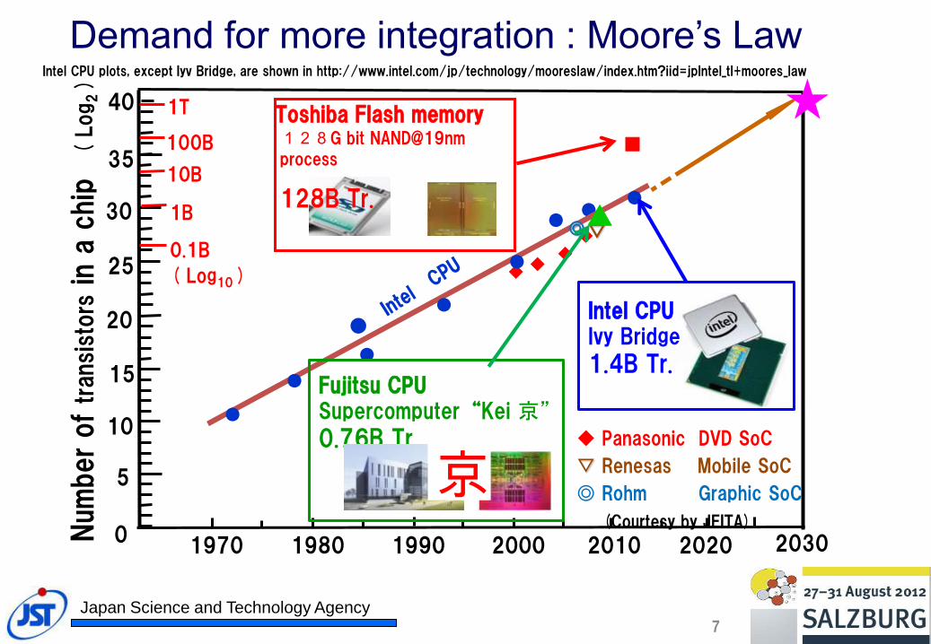
Demand for more integration : Moore’s Law
7
Intel CPU plots, except Iyv Bridge, are shown in http://www.intel.com/jp/technology/mooreslaw/index.htm?iid=jpIntel_tl+moores_law
1970 1980 1990 2000 2010 2020 0
5
15
10
20
25
30
35
( L
og
2 )
◆
◆ Panasonic DVD SoC
▽ Renesas Mobile SoC
◎ Rohm Graphic SoC
(Courtesy by JEITA)
▽ ◆
◆ ◆
● ●
●
●
●
●
●
▲ ◎
40
2030
■
Num
ber
of
transi
stors
in a
chip
1B
0.1B
10B
100B
1T
●
Intel CPU Ivy Bridge
1.4B Tr. Fujitsu CPU Supercomputer“Kei 京”
0.76B Tr.
Toshiba Flash memory ★
( Log10 )
128G bit NAND@19nm
process
128B Tr.
京
Japan Science and Technology Agency

Japan Science and Technology Agency 8
Demand for more miniaturization Gate
length
(nm
)
1
101
★
★
★
▲ ▲
▲
▲ ▲
★ ★
▲ ▲ ▲
★
★ ★ ★ ★ ★
▲
▲
1970 1980 1990 2000 2010 2020 0.1
Lg=6nm @2020
World-smallest MOS Lg=5nm
★
▲
Quantum -scaling
Nanowire Nanopillar Nanosheet
Dennard -scaling
Booster -scaling
Lg
SiON-base High-k Low-k Metal G Strain
Fin SOI
Planar Si-channel CMOS
3D -scaling
▲
放熱経路放熱経路
シングルピラー マルチピラー
2030
Lg=1nm @2030
▲
104
103
102
Lg=1nm ⇒ Four Si-atom length
High-μ -scaling
Ge III-V
?

ERM (Emerging research materials)
• ITRS assigned the following materials as ERM. • Low Dimensional Materials(Nano-mechanical memory, Nanotube,
Nanowire, Graphene・・・)
• Macromolecules(Molecular memory, Molecular devices, Resists, Imprint
polymers・・・)
• Self-Assembled Materials(Sub-lithographic patterns, selective etch・・・)
• Spin Materials (MRAM by spin injection, Semiconductor spin transport, FM
semiconductors・・) (Spin-injection MRAM is already out of ERM in 2012)
• Multiferroics (Complex Metal Oxides)
• Interfaces and Heterointerfaces (Electrical and spin contacts)
Japan Science and Technology Agency 9

How the Project was designed
• According to the ITRS roadmap Japanese government determined Nanoelectronics Projects
• METI / NEDO MIRAI Ⅲ project (from 2006 FY)
• METI Nanoelectronics project Non-Si channel, Nanowire, XMOS (from 2007FY)
• MEXTStrategic Sectors for beyond CMOS (2007FY)
– JST Sato-PRESTO project
– JST Watanabe-CREST project
• Cabinet selected 30 Researchers for Cutting Edge Research Support Program(FIRST)(Yokoyama, Ohno, Arakawa, Esashi, Kawai, ・・・)(2009FY)
• Tsukuba Innovation Arena (TIA)[Japanese version of IMEC](METI, MEXT, AIST, NIMS, Tsukuba Univ.)
•
Japan Science and Technology Agency 10

Strategic Sector (Target of Research) from MEXT for Next-Generation Devices
• “Research and development of materials and nano-processes to realize devices with novel concept, novel functionality and novel structure”
• It lists following fields as important targets 1. Development of non silicon materials for beyond-CMOS
2. Pioneering materials for novel concept-devices by using combined functionalities of photon, electron and spin
3. Development of novel devices based on nano-scale fabrication
4. Development of thin flexible resilient materials
Japan Science and Technology Agency

Japan Science and Technology Agency
METI Nanoelectronics project (Non-Si channel, Nanowire, XMOS)
12
Japan’s National Projects for Next
Generation Nanoelectronics Devices 2006 2007 2008 2009 2010 2011 2012 2013 2014 2015
METI / NEDO MIRAI Ⅲproject
Cabinet’s Cutting Edge Research Support Program (FIRST) 30 Researchers
(Yokoyama, Ohno, Arakawa, Esashi, Kawai, ・・・)
METI, MEXT, AIST, NIMS, Tsukuba Univ.
Tsukuba Innovation Arena (TIA)
FY
JST Watanabe-CREST project (2007start)
JST Watanabe-CREST project (2008start)
JST Watanabe-CREST project (2009start)
JST
CREST
JST
PRESTO
JST Sato-PRESTO project
JST Sato-PRESTO project
JST Sato-PRESTO project
Personal Type
Team Type
METI
MEXT/JST

Sato-PRESTO Project
• The PRESTO* project “Materials and Processes for Next Generation Innovative Devices” started in 2007 FY
• The scope of this project involves • Spintronics devices and materials
• Semiconductor nano-electronics
• Wide-gap semiconductors
• Molecular and organic electronics
* Precursory Research for Embryonic Science and Technology (Sakigake)
13
Japan Science and Technology Agency 13

Organization
Suprevisor
Advisors
33 Researchers
stage (1): 11, stage (2): 10, stage (3): 12
JST Staffs
Office
Research Manager
Administrative Manager
14

Duration and Budgets
• Duration: 3.5 years
• Budget: 40MYen (~400KEuros) per person
• Members: 33 (Total 1.4BYen~14MEuro)
• Average age at adoption: 34.5 years old
• Affiliation: Universities: 25, Government Agencies: 8
For Comparison: Case of Watanabe-CREST Duration Max 5.5 years Budget 150-500 M Yen (1.5-5 M Euro) per team Teams: 18
Japan Science and Technology Agency 15

Research Themes
(1st stage) 11 themes
Researchers Research Themes
S. Kasai Research on stochastic resonance nanodevices and their integration for novel noise-robust information processing systems
E. Saitoh Spintronics based on spin currents and spin-photon coupling in dielectrics
S. Shiraishi Spin current control in molecules
Y. Takahashi Development of half-metal at RT for spintronics devices
T. Taniyama Control of spin polarization and its application to tunable spin sources
A. Tsukamoto Ultrafast manipulation and measurement of spin dynamics by femtosecond laser pulse
N. Fukata Development of semiconductor nanowires for the realization of vertical three-dimensional semiconductor devices
S. Murakami Unified theory of spin and heat currents and its applications
T. Yasuda High-performance organic field-effect transistors using intrachain carrier transport along uniaxially aligned p-conjugated polymers
A. Yamaguchi Study in novel electromagnetic properties of modulated and/or periodic magnetic strucure composed of nanoscale magnets
K. Wakabayashi Design and physical properties forecast of nano-carbon electronic devices based on computational methods
spintronics wide-gap semiconductor molecules/organics others

Research Themes
(2nd stage) 10 themes
Researchers Research Themes
R. Katayama Novel optical function using photonic nano-structure of polar wide-gap semiconductors
I. Kawayama Creation of an optically-generated-flux-quantum nano-device with superconducting
nanobridges
Y. Kangawa Fabrication of III-nitride substrate for optoelectronic integrated circuit and control of its heat transfer
W. Kobayashi Development of materials for thermoelectronics
T. Susaki New functionalities at the interfaces of wide-gap oxides
M. Takenaka Ge Nano Electro-Optic LSI for intrachip optical interconnects
T. Nakaoka Charge/spin/photon hybrid single-electron device based on quantum dot
K. Hamaya Development of single-electron spin transistors with silicon-based nanostructures
T. Fukumura Wide-gap ferromagnetic semiconductor devices
N. Mizuochi Quantum information devices by single paramagnetic color center in wide-bandgap semiconductor
spintronics wide-gap semiconductor molecules/organics others

Research Themes
(3rd stage) 12 themes
Researchers Research Themes
H. Kaiju Creation of novel high-performance non-volatile memory using spin quantum cross devices
H. Kumigashira Development of memory with low environmental stress using nano-capasitor structure
Y. Takahashi Silicon Raman laser using photonic crystal nanocavity
K. Tomioka Control of Si/III-V super-heterointerface and development of nanowire-based tunneling FETs
K. Nakano Development of high-performance organic field-effect transistors through the control of molecular arrangement
H. Nakano Spin manipulation in dielectric-channel transistors J. Nishinaga New devices using fullerene / III-V compound semiconductor heterostructures
H. Noguchi Development of organic single-electron transistors controlled by photo-induced gate signal
S. Noda Facile implementation of nanocarbons with selectable higher-order structures
M. Higashiwaki Interface control and device application of III-oxide/nitride semiconductor composite structures
T. Machida Physics and application of quantum dot devices based on graphene
H. Yamamoto Development of novel organic devices based on electronic correlation
spintronics wide-gap semiconductor molecules/organics others

Fields
Charge
Heat
Spin
Light
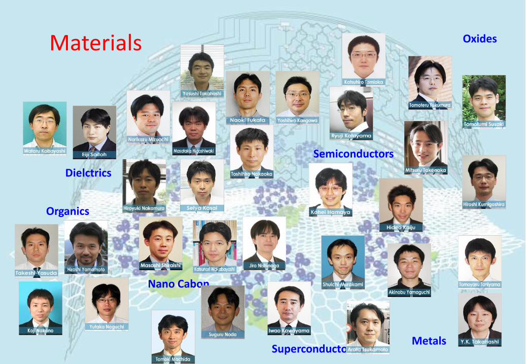
Materials
Semiconductors
Metals
Organics
Dielctrics
Superconductor
Oxides
Nano Cabon
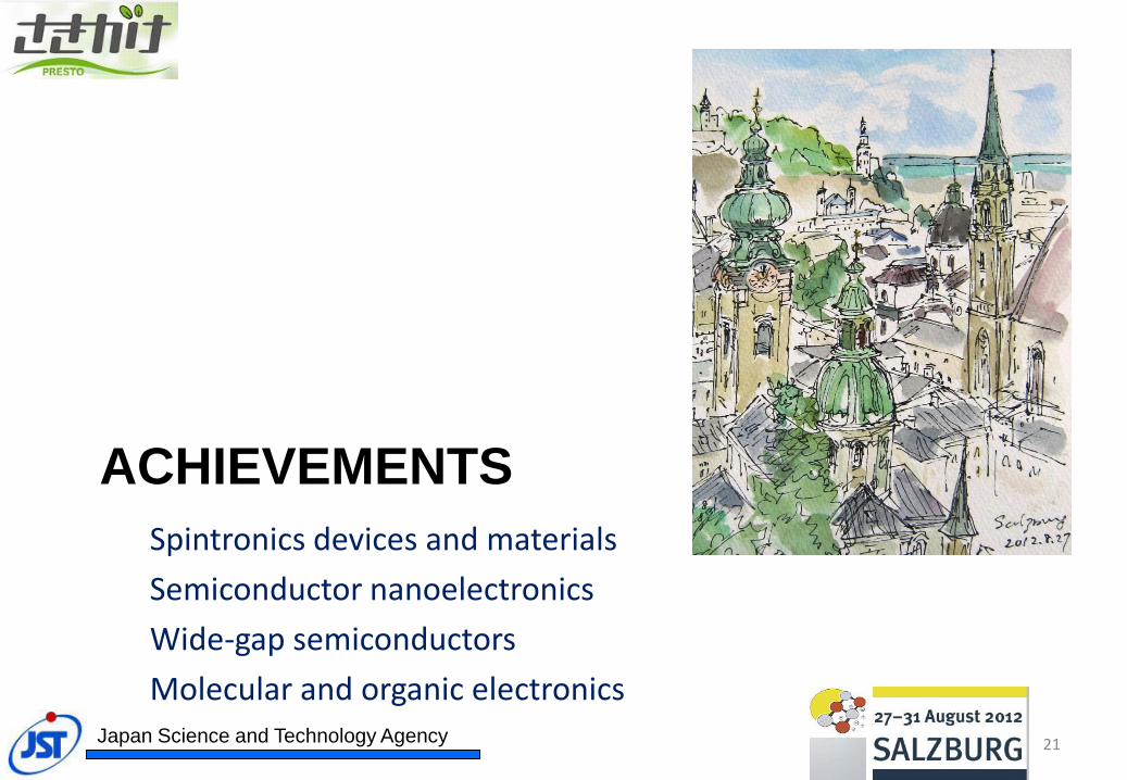
ACHIEVEMENTS
Spintronics devices and materials
Semiconductor nanoelectronics
Wide-gap semiconductors
Molecular and organic electronics
21 Japan Science and Technology Agency

Spintronics devices and materials
1. Y. Takahashi developed Heusler alloy Co2Mn(Ga,Ge) with the highest degree of spin polarization
2. E. Saitoh succeeded in transfering DC signal through insulator by using spin current. He discovered Spin Seebeck effect by using thermal spin current
3. S. Murakami proposed unified theory of spin and heat and predicted high thermoelectric performance in topological insulators
4. S. Shiraishi succeeded in spin injection to single sheet of graphene 5. T. Fukumura succeeded in controlling magnetic properties by gate-
voltage in room temperature ferromagnetic semiconductor TiO2:Co
Japan Science and Technology Agency

HIGH SPIN POLARIZATION SPIN SOURCE
Spintronics devices and materials
23 Japan Science and Technology Agency

Half metal electrodes for MTJ
EF
http://www.riken.go.jp/lab-www/nanomag/research/heusler_e.html
• Half metal is a magnetic material in which electronic state for spin is metallic while that for spin is semiconducting.
• Therefore the electronic state at the Fermi level is fully spin-polarized in half metals.
• Heusler compounds, LSMO (La1-
xSrxMnO3), magnetite (Fe3O4), chromium oxide (CrO2) are candidates of half metals.
LSMO Half Heusler
Full Heusler Magnetite
CrO2
CrAs
24

Heusler Alloys
• The Heusler alloys are classified into two groups by their crystal structures; – Half Heusler alloys with XYZ-
type in the C1b structure (a) – Full Heusler alloys with X2YZ-
type in the L21 structure (b) where X and Y atoms are transition metals, while Z is either a semiconductor or a non-magnetic metal.
Half Heusler alloy
XYZ type C1b str.
Full Heusler alloy
X2YZ with L21 str.
Disordered derivatives
B2-structure with
Y-Z disorder
A2-structure with
X-Y and X-Z disorder
http://www.riken.go.jp/lab-www/nanomag/research/heusler_e.html 25

TMR with full Heusler X2YZ alloys
26

Control of Ef
P=0.5
P=0.75
Control of DOS(Ef)
L21 X2YZ B2 X(Y or Z) A2 X or Y or Z High Tc Theoretical P=1
However, Experimental P is low
Co based Heusler alloy、X2YZ
Alloy search for RT half-metal
Full order
Disorder
27

Search of high spin-polarization half metals using PCARS
• Aiming at high performance GMR devices Takahashi has investigated as many as 32 full Heusler alloys and found 74% sipn polarization in CoMnGeGa alloy.
Ternary
alloys
P Ref
.
Co2MnSi 56
Co2MnGe 58
Co2MnSn 60
Co2MnAl 60
Co2MnGa 60
Co2CrAl 62
Co2FeAl 59
Co2FeSi 60
Co2FeGa 58
Co2CrGa 61
Co2TiSn 57
Co2VAl 48
Fe2VAl 56
Quaternary alloys P Ref.
Co2Mn(Ge0.75Ga0.25) 74
Co2Mn(Ga0.5Sn0.5) 72
Co2Fe(Si0.75Ge0.25) 70
Co2FeGa0.5Ge0.5 68
Co2(Cr0.02Fe0.98)Ga 67
Co2MnGeSn 67
Co2(Mn0.95Fe0.05)Sn 65
(CoFe)2MnGe 65
Co2(Mn0.5Fe0.5)Ga 65
Co2(Cr0.02Fe0.98)Si 65
Co2MnTiSn 64
Co2MnAl0.5Sn0.5 63
Co2MnGaxSi1-x 63
Co2FeAlGa 63
Co2MnSiGe 63
Co2(Mn0.5Fe0.5)Si 61
Co2Mn(Al0.5Si0.5) 60
Co2FeGa0.5Si0.5 60
Co2Fe(Al0.5Si0.5) 60
Metals and
binary P Ref.
Fe 46
Co 45
FeCo 50
Co75Fe25 58
B2-FeCo 60
[Co/Pd]n 60
Japan Science and Technology Agency 28

Search of Heusler alloys following band calculation
Co2MnGa1-xSnx 29

Point contact Andreev reflection (PCAR)
V
Lock-in Amp.
Digital
MultimeterPoint-contact
Potentiometer
(1-100)
1
30
AC modulation 2kHzinternal oscillator
DC biasFunction synthesizer
GND
V
Lock-in Amp.
Digital
MultimeterPoint-contact
Potentiometer
(1-100)
1
30
AC modulation 2kHzinternal oscillator
DC biasFunction synthesizer
GND
-6 -4 -2 0 2 4 6
0.0
0.2
0.4
0.6
0.8
1.0
1.2
1.4
1.6
1.8
2.0
2.2
P = 1.0
P = 0.35
P = 0.0
Z = 0.0
= 1.5meV
V(mVolt)
G(V
)/G
n
Nb
Sample
Co2MnGe0.75Ga0.25 shows highest P
Japan Science and Technology Agency 30

SPIN CURRENT
Spintronics devices and materials
31

A magnetic insulator transmits electrical signals via spin waves
• Saito succeeded in transmitting electric signals through YIG using spin waves (pure spin current) in the insulator.
• The spin Hall effect, which converts the charge current to a spin current, and its inverse forms the basis for a proof of principle. (cited in Physic Today)
Y. Kajiwara, K. Harii, S.
Takahashi, J. Ohe, K. Uchida,
M. Mizuguchi, H. Umezawa, H.
Kawai, K. Ando, K. Takanashi,
S. Maekawa & E. Saitoh,
Nature 464 262 (2010)
32

Spin relaxation
Spin wave spin current
Excitation
・local FMR
・electrical excitation
(oscillating current+ME)
Detection
・spin torque meter
・Faraday effect
・electrical detection(ISHE)
Excitation, modulation and detection of spin wave spin current
Dielectrics
・application of electric field
・strong interaction with photon
Modulation
・electric field+SO
Japan Science and Technology Agency 33

Spin current and heat flow
• Saito et al. observed the spin voltage generated from a temperature gradient in a metallic magnet and name the phenomenon as spin-Seebek effect using a recently developed spin-detection technique that involves the SHE.
– K. Uchida, S. Takahashi, K. Harii, J. Ieda, W. Koshibae, K. Ando, S. Maekawa and E. Saitoh: Nature 455 (2008) 778.
34

35
35
Seebeck and “spin-Seebeck” effects
Spin
voltage
Two spin channels (up / down)
with different Seebeck coefficients
Two conductors with different Seebeck coefficients
depending on the density of electrons
Electric
voltage
+ spin currents
spin voltage
voltage
35

Observation of spin-Seebeck effect
ISHE voltage induced by
the spin-Seebeck effect
Magnetic field dependence of V Spin voltage
electromotive force of opposite signs
Spin voltage of opposite sign
using the inverse spin-Hall effect (ISHE)
K. Uchida, E. Saitoh et al. Nature (2008).
NiFe
Pt
36

Spin Seebeck insulator
• Saito succeeded in observing spin Seebeck effect in insulating LaY2Fe5O12
K. Uchida, E. Saitoh et al.: Nature Mat. (online Sept 27, 2010)
Japan Science and Technology Agency 37

Graphene Spintronics
Graphene
1. Generation of a
pure spin current
2. Injection of spins in
graphene
at ROOM
TEMPERATURE
Gate-induced Modulation of Spin Signals
in single-layer graphene
Pure Spin Current !!
Japan Science and Technology Agency M. Shiraishi, "Graphene Spintronics", "Graphene : The New Frontier" (World Scientific Press, 2010/6/22).
Single-layer graphene
38

Graphene Spintronics
,)][sinh()()1(
2 1
22
2
inject
sf
F
N
Flocalnon I
LR
R
R
P
PV
M. Ohishi, M.Shiraishi et al., JJAP 46, L605 (2007).
M. Shiraishi et al., Adv. Func. Mat.,19, 3711 (2009) .
M. Shiraishi et al., Appl. Phys. Express 2, 123004 (2009).
Spin polarization is CONSTANT.
Better
robustness
than that in
MgO-TMR
Japan Science and Technology Agency 39

Silicon Spintronics
• For application of spintronics, combination with Si technology is very important.
• Previous studies of Si spintronics used only highly doped metallic Si, which is not suited for gate-control devices.
• Hamaya successfuly utilized low-doped Si for spintronics application.
M. Ishikawa, H. Sugiyama, T. Inokuchi, K. Hamaya, Y. Saito, "Effect of the interface resistance of CoFe/MgO contacts on spin accumulation in silicon", Appl. Phys. Lett. 100, 252404 (2012).
40

TOPOLOGICAL INSULATOR
Spintronics devices and materials

3) Quantum spin Hall systems as candidates for efficient thermoelectrics
Theory of spin current and heat current
* suppress phonon conduction, keeping electron conduction * Low-dimensional states (edge states, surface states) * Similar materials involved (Bi1-xSbx, Bi2Se3 etc.)
2D Spin current
Quantum spin Hall systems can be good thermoelectrics at low temp.
1) Bismuth ultrathin films as quantum spin Hall phases 2) Universal Phase Diagrams for 2D and 3D quantum spin Hall phases
Low T High T
TSZT
2
r=“ bulk/edge ” g=“ phonon/bulk ”
• Lower temp. longer inelastic scattering length for edge states edge states become dominant bulk-to-edge crossover of thermoelectric transport • Ultrathin & narrow ribbon (of QSH system) crossover occurs at around 10K
Result
Expectation : QSH systems can be good thermoelectric.
Japan Science and Technology Agency R. Takahashi, S. Murakami: Phys. Rev. B, 81, 161302 (2010)

Quantum spin Hall state
Odd number of Kramers pairs of edge states
bulk
bulk
bulk
bulk
Zigzag edge
Armchair edge
スピンはほぼ薄膜面に垂直 (// z) 10%-20% 程度傾いている
x
y
スピン: xz 面内
x
y
bulk
(a) (111) 1-bilayer: spin polarization on edges
スピン: xz 面内

{012} 2-monolayer= insulating phase (111) 1-bilayer = quantum spin Hall phase
• Thermoelectric figure of merit
• In the quantum spin Hall phase, figure of merit ZT of thermoelectric conversion is determined by the balance between the edge and the bulk. • ZT is large if the chemical potential is close to the band edge. • ZT is large if the length of system is long. edge states dominantly determine ZT. • ZT increases with temperature. Higher energy carriers contribute to ZT.
Idealized model (perfect conductor on the edge)
Theoretical Approach Quantum Spin Hall Effect in Bismuth
– Bulk Bi show no gap, while edge is gapless. – Bi ultra thin film (topological insulator)
TSZT
2
Japan Science and Technology Agency
Wada, Murakami: "Well-localized edge states in two-dimensional topological insulator: bismuth film", APS March Meeting 2010(2010), Oregon, USA (2010/3/15).

MAGNETIC SEMICONDUCTOR
Spintronics devices and materials
45

High TC FM semiconductor:
cobalt-doped TiO2
Science (2001)
Extraordinary high TC
TiO2:Co Room temperature FM
semiconder
Giant MO effect at RT
T. Fukumura, Jpn. J. Appl. Phys. (2003)
H. Toyosaki, Appl. Phys. Lett. (2005)
Anomalous Hall effect at RT
H. Toyosaki, Nature Mater. (2004)
T. Fukumura, Jpn. J. Appl. Phys. (2007)
Tunneling Magnetoresistance
H. Toyosaki, Jpn. J. Appl. Phys. (2005)
CdGeP2:Mn ZnO:Co GaN:Gd,,,
Zn1-xTMxO combinatorial library G.A. Medvedkin, T. Ishibashi, T. Nishi, K. Hayata, Y. Hasegawa and K. Sato: Jpn. J. Appl. Phys. 39 Part 2 [10A] (2000) L949-L951
Japan Science and Technology Agency 46

Carrier control of magnetism in TiO2:Co
by gate voltage
Japan Science and Technology Agency 47
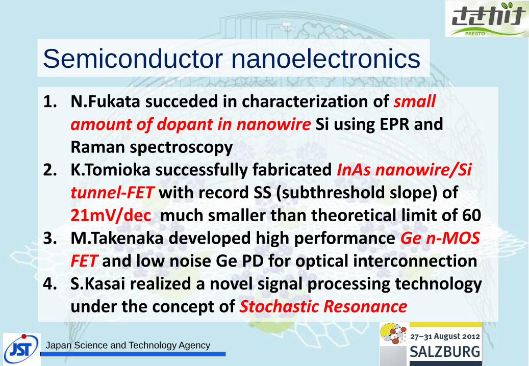
Semiconductor nanoelectronics
1. N.Fukata succeded in characterization of small amount of dopant in nanowire Si using EPR and Raman spectroscopy
2. K.Tomioka successfully fabricated InAs nanowire/Si tunnel-FET with record SS (subthreshold slope) of 21mV/dec much smaller than theoretical limit of 60
3. M.Takenaka developed high performance Ge n-MOS FET and low noise Ge PD for optical interconnection
4. S.Kasai realized a novel signal processing technology under the concept of Stochastic Resonance
Japan Science and Technology Agency

NANO-WIRE TRANSISTORS
Semiconductor Nanoelectronics
49 Japan Science and Technology Agency
Drain
Source
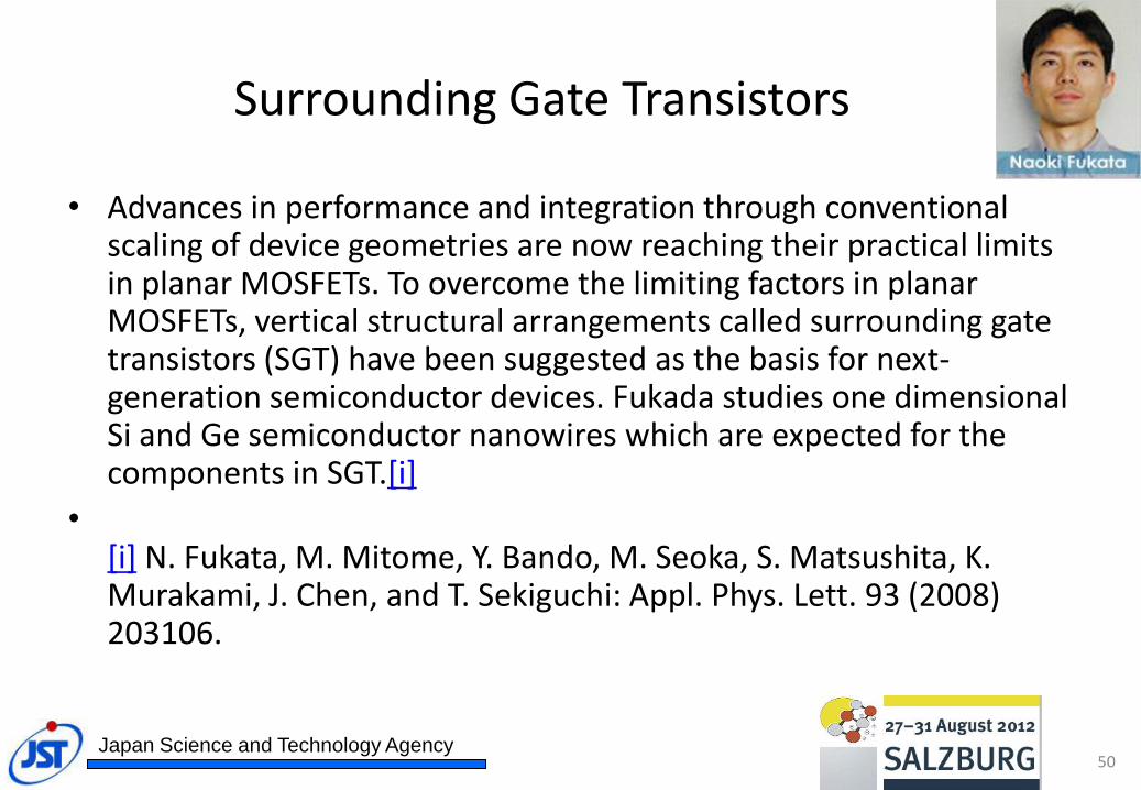
Surrounding Gate Transistors
• Advances in performance and integration through conventional scaling of device geometries are now reaching their practical limits in planar MOSFETs. To overcome the limiting factors in planar MOSFETs, vertical structural arrangements called surrounding gate transistors (SGT) have been suggested as the basis for next-generation semiconductor devices. Fukada studies one dimensional Si and Ge semiconductor nanowires which are expected for the components in SGT.[i]
• [i] N. Fukata, M. Mitome, Y. Bando, M. Seoka, S. Matsushita, K. Murakami, J. Chen, and T. Sekiguchi: Appl. Phys. Lett. 93 (2008) 203106.
50 Japan Science and Technology Agency
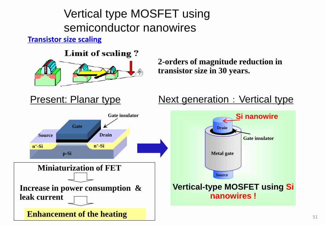
Vertical type MOSFET using
semiconductor nanowires
Metal gate
Gate insulator
Drain
Source
Si nanowire
p-Si
n+-Si n+-Si
Gate
Gate insulator
Source Drain
Present: Planar type Next generation:Vertical type
Vertical-type MOSFET using Si nanowires !
2-orders of magnitude reduction in transistor size in 30 years.
Transistor size scaling
Enhancement of the heating
Miniaturization of FET
Increase in power consumption & leak current
51

Synthesis & Impurity doping in Si nanowires
First observation of B local vibrational peak
and Fano effect in B-doped SiNWs
SiOx
Si
SiOx B doping
First observation of conduction electron
signals in P-doped SiNWs
g=1.998:
Conduction electrons
g=2.005:
Interfacial defects
Inte
nsity
(arb
. un
its)
324 322 320 318
Magnetic field (mT)
P-doped SiNWs
Undoped SiNWs
40nm
Inte
nsity
(arb
. uni
ts)
650600550500
Raman shift (cm-1
)
Bulk Si
B-doped SiNWs
undoped SiNWs Fano effect
P doping
Formation of p-type SiNWs Formation of n-type SiNWs
EPR
Raman
52

InAs nanowire Tunnel FET
• Tomioka succeeded in fabricating a Tunnel MET using InAs nanowire on Si substrate by MOVPE through holes fabricated on SiO2 insulator by electron beam lithography.
53 Japan Science and Technology Agency

How the InAs nanowire TFET works
• Figure illustrates TFET using III-V NWs/Si heterojunctions. Each TFETs are composed of a combination of III-Vs and Si in order to utilize Zener tunnel mechanism working at a band discontinuities across the III-V and Si junctions.
54 Japan Science and Technology Agency
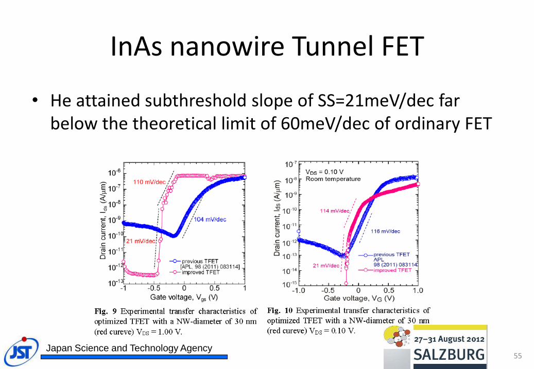
InAs nanowire Tunnel FET
• He attained subthreshold slope of SS=21meV/dec far below the theoretical limit of 60meV/dec of ordinary FET
55 Japan Science and Technology Agency

Nanowire FET with core-shell HEMT structure
• Tomioka fabricated high performance FET using InAs nanowire with core-shell HEMT structure.
56 Japan Science and Technology Agency

For optical interconnects
• Transmission delay of wiring in a chip is a serious problem limiting the performance of the LSI. Intrachip optical interconnects will make it possible to enhance the performance of LSIs even in the post-scaling era. Takenaka is aiming at establishing fundamental technologies for one-chip super computers and photonic router chips using monolithic integration of Ge MOSFETs and Ge photodetectors on a Si substrate.[i]
• [i] M. Takenaka, S. Tanabe, S. Dissanayake, S. Sugahara, S. Takagi: 21st Annual Meeting of the IEEE Laser & Electro-Optics Society, Newport Beach, US (2008) Paper MN2.
57 Japan Science and Technology Agency

Ge-based LSI with on-chip optical interconnects
GOI MOSFET +
Monolithic integration:
MSM Ge PD
Si sub.
SiO2
Ge Ge
Ge based LSI with on-chip
optical interconnects
0.1
1
10
100
1000
0 0.2 0.4 0.6 0.8 1
De
tecto
r cu
rre
nt
[nA
]
Voltage [V]
Ge detector
10m
NiGe NiGe
Ge PD GOI MOSFET
0
1x10⁻⁴
2x10⁻⁴
3x10⁻⁴
4x10⁻⁴
5x10⁻⁴
6x10⁻⁴
7x10⁻⁴
8x10⁻⁴
-7 -6 -5 -4 -3 -2 -1 0
Dra
in c
urr
en
t [A
]
Drain voltage [V]
L = 10 m
W = 30 m
58 Japan Science and Technology Agency

STOCHASTIC RESONANCE
Semiconductor Nanoelectronics
59 Japan Science and Technology Agency
Stochastic Resonance
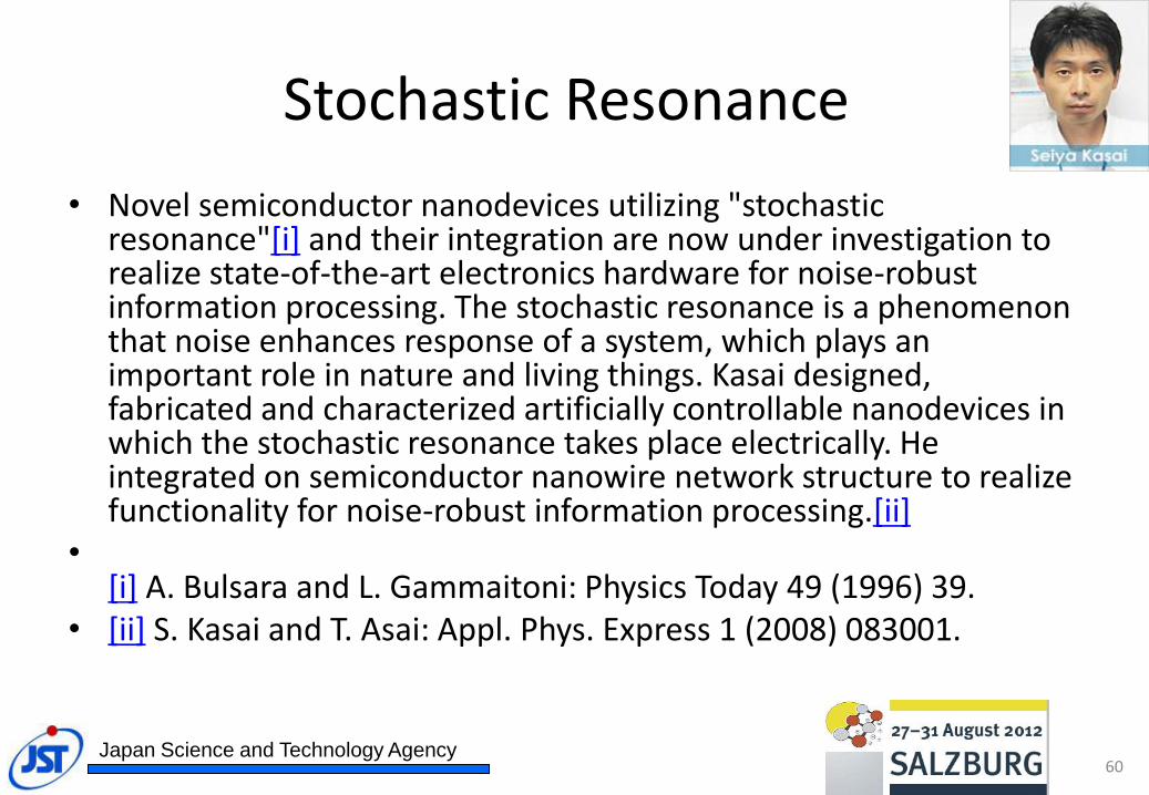
• Novel semiconductor nanodevices utilizing "stochastic resonance"[i] and their integration are now under investigation to realize state-of-the-art electronics hardware for noise-robust information processing. The stochastic resonance is a phenomenon that noise enhances response of a system, which plays an important role in nature and living things. Kasai designed, fabricated and characterized artificially controllable nanodevices in which the stochastic resonance takes place electrically. He integrated on semiconductor nanowire network structure to realize functionality for noise-robust information processing.[ii]
• [i] A. Bulsara and L. Gammaitoni: Physics Today 49 (1996) 39.
• [ii] S. Kasai and T. Asai: Appl. Phys. Express 1 (2008) 083001.
60 Japan Science and Technology Agency

Japan Science and Technology Agency
Improvement of SNR by using noise
• Stochastic resonance improve grey scale reproduction
High contrast but lose grey scale
recover grey scale by addition of noise
61

Stochastic Resonance in Nanowire FET Network
GaAs etched
nanowire
Output
Input
VDD
Wrap gate
Noise
Stochastic resonance (SR) is a phenomenon that many bio-systems
use to enhance their response in noisy environment.
The SR was realized in GaAs nanowire FET networks and enhanced
weak-signal detection was successfully demonstrated.
S.Kasai et al., Appl. Phys. Express 1, 083001 (2008)
62
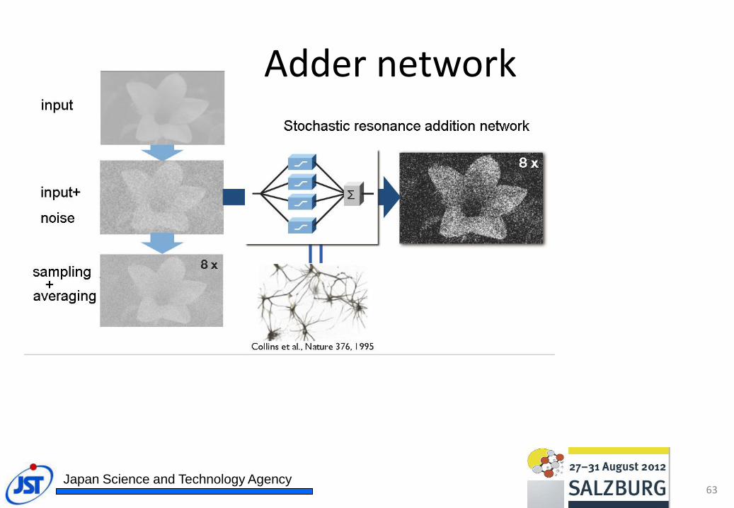
Adder network
63 Japan Science and Technology Agency

Scatter of threshold
Uniform Threshold With scatter of threshold 64
Japan Science and Technology Agency

Wide-gap semiconductors
1. N.Mizuochi succeeded in room temperature operation of quantum information processing solid state device and current-induced single photon source by using NV center in diamond p-i-n junction
2. Y.Kangawa succeeded in LPE growth of AlN single crystal for III-N substrate using solid state nitrogen source (LiN)
3. R. Katayama fabricated GaN thin film with periodic modulation of polarity for nonlinear optics
4. M.Higashiwaki succeeded in fabricating Ga2O3 –based device for power electronics
Japan Science and Technology Agency

QUNTUM INFORMATION PROCESSING USING DIAMOND NV CENTER
Wide Gap Semiconductors
66 Japan Science and Technology Agency

Single NV center in diamond
NV center: (NV-, 6 electrons, C3v)
・Ground state: spin triplet(electron spin S=1)
・Long coherence length.
・Observation of single NV center and single spin manipulation is possible
・Initialization of electron spin states by light irradiation is possible
Quantum information processing solid state device for
room temperature operation (Quantum register, Quantum repeater, single photon emitter …)
67 Japan Science and Technology Agency

Measurement Instruments for
single NV center
Fluorescent image of single NV center by confocal laser microscope
Anti-bunching measurement using Hanbury-Brown Twiss interferometer
AO modulator Monochromator CCD detector
Objective
lens
sample
Piezo- electric stage
Magnet
Power source
68 Japan Science and Technology Agency

Multiple quantum bit Quantum resister: multiple q-bits of single NV-center
13C-doped system
Experimental and simulated ODMR spectra of nearest neighbor carbon atoms assigned as consisting of (a)0, (b)1, (c)2, (d)3 13C-center(s)
N:nitrogen.V: Vacancy (V). Carbon atoms labeled at 1-3 are called as nearest-neighbor carbon atom from vacancy.
Jiang et al., PRA 76, 062323 (2007)
G. Balasubramanian, P. Neumann, D. Twitchen, M. Markham, R. Kolesov, N. Mizuochi, J. Isoya, J. Achard, J. Beck, J. Tissler, V. Jacques, F. Jelezko, J. Wrachtrup, "Ultralong spin coherence time in isotopically engineered diamond", Nature materials, v. 8, p. 383-387 (2009) 69

Room temperature single photon emission from NV0 center in diamond LED • Mizuochi succeeded in
observing single photon emission from p-i-n light emitting diode of diamond.
EL image of single NV center N. Mizuochi, T. Makino, H. Kato, D. Takeuchi, M. Ogura, H. Okushi, M. Nothaft, P. Neumann, A. Gali, F. Jelezko, J. Wrachtrup, S. Yamasaki, "Electrically driven single photon source at room temperature in diamond", Nature Photonics, 6, 299-303 (2012). 70

1. K. Wakabayashi theoretically predicted edge state spins in nano structured graphene
2. H. Yamamoto fabricated organic FET with high field effect mobility using voltage controlled Mott-transition. He also succeeded in electrical control of superconductivity in organic material
3. S. Noda succeeded in growing single graphene sheet on insulating substrate by metal-free process
4. J. Nishinaga succeeded in delta-doping of C60 in GaAs thin film during MBE growth
Molecules and Organics
Japan Science and Technology Agency

GRAPHENE ELECTRONICS
Molecules and Organics
72 Japan Science and Technology Agency

New class of quantum wires
Graphene nanoribbons and
strong nanoscale effect
Armchair ribbons
Zigzag ribbons
M. Fujita, K. Wakabayashi, K. Nakada, K. Kusakabe, J. Phys. Soc.
Jpn. (1996).
K. Nakada, M. Fujita, et. al. Phys. Rev. B (1996).
K. Wakabayashi, M. Fujita, et. al., Phys. Rev. B (1999).
t=2.7eV
ferrimagnetic spin
correlation Crossover from dia- to
para magnetism
73

Perfectly Conducting Channel
dimensionless conductance:
ensemble average for various impurity
configuration
#of samples > 10000
Averaged conductance <g> converges to 1.
Perfectly Conducting Channel
K. Wakabayashi et. al., PRL(2007), Carbon(2009),
PRB(2009)
Absence of Anderson localization
74

(1) Multiple zero conductance dips appear
in ZZZ junction, which serve as the charge current
switching.
(2) Visible condition at T=300K : W< 12.5nm
NL=20, NR=14 ZAZ ZZZ
Electronic transport through
graphene junction
App. Phys. Lett. (2009) Internal circular current is induced at the energy
in the vicinity of zero conductance dips.
A: armchair
Z: zigzag
Lead Junction Position of anti-resonance
A A
Z
Z A
just before 2ch. is opened
in wider ribbon.
Z
75

Graphene Quantum Dot
Ultra high sensitivity THz detector
Room temperature SET
Q-dot spin valve
- Parallel double q-dot - Single electron transistor+quantum Hall effect
- Local anode oxidation using AFM
- FM electrode+Graphene Q-dot
76

Ultra high sensitivity THz detector
Q-Hall effect+Single electron tunneling +Cyclotron resonance
h
77

Landau quantization:Dirac Fermion v.s. electron
-200
-100
0
100
200
Ene
rgy
(meV
)
1086420
B (T)
Dirac Fermion
60
50
40
30
20
10
0
Ene
rgy
(meV
)
1086420
B (T)
Electron
eBncEn 2~ Bm
enEn *2
1
nh
exy
22
2
14 2
nh
exy
Linear Nonlinear
78
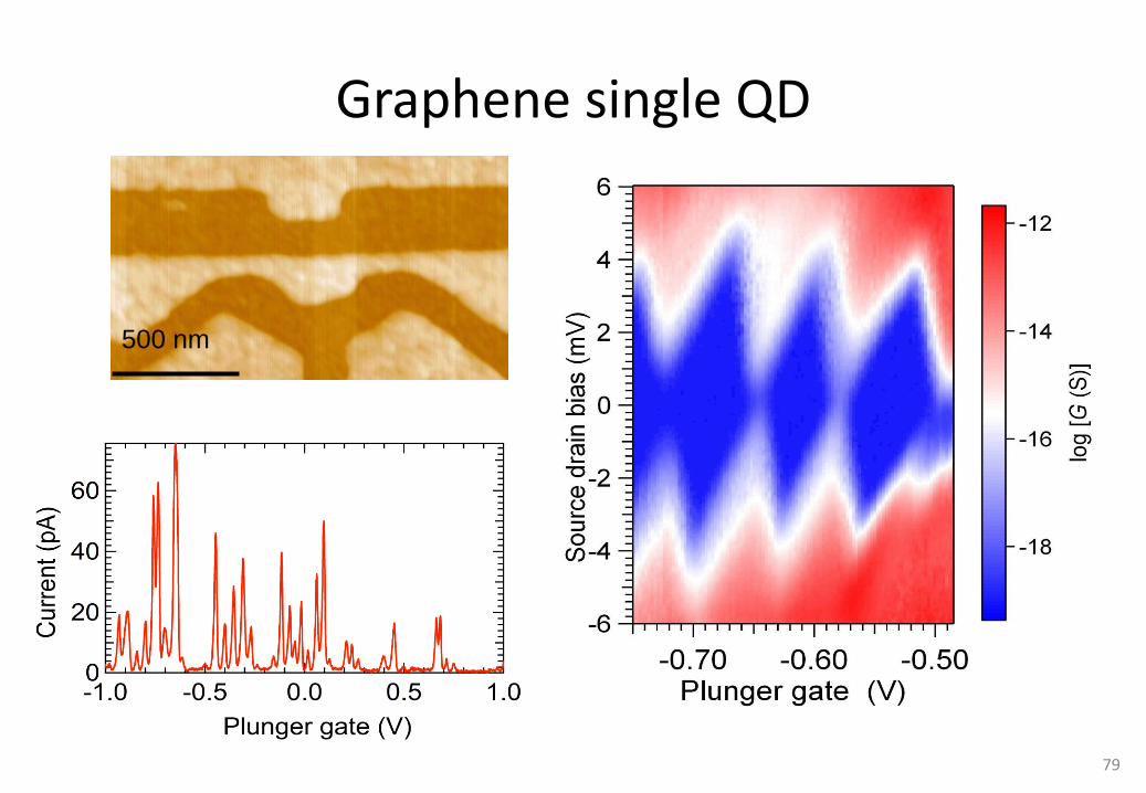
79
Graphene single QD
79
500 nm
79

Nonlocal Magnetoresistance
B 5m
NM
F NM
F
VBG = 30 V, T = 2 K
4
2
0
-2
-4
RN
L (
)
-200 0 200
B(mT)
Graphene
F F
FM/Graphene/FM
Spin valve Without barrier
80

Graphene spin valve with tunnel barrier
-98
-96
-94
-92
-90
RN
L (
)-100 0 100
B(mT)
T = 5 K, VBG = -30V
FM/Al2O3/graphene/ Al2O3/FM
Spin valve
d = 10 ML
Al2O3 barrier by ALD
81

ORGANIC FET USING ELECTRONIC CORRELATION
Molecules and Organics
82 Japan Science and Technology Agency

-Br (Cu[N(CN)2]Br-1) crystal structure
Organic FET structure
83

Temperature dependence of carrier mobility
gdV
d
C
1
84

Gate-voltage dependence of carrier concentration
計算より求めた
-Br のフェルミ面 90% of 1st BZ carriers appear by application of gate
voltage of 40V assuming 1monolayer active layer
T = 20 K
85

Other achievements
1. H. Kumigashira succeeded in 2D-confineiment of strongly-correlated electrons
2. W. Kobayashi developed thermal diode with the record rectification ratio
3. A. Tsukamoto succeeded in ultra-high speed magneto-optical recording by using circularly polarized pulse-laser of sub-pico second width
Japan Science and Technology Agency

Light-Induced ultrafast magnetization reversal
• The response time of magnetization reversal is usually limited by the spin dynamics which follow Landau-Lifshitz-Gilbert equation.
• By a collaboration of Nihon Univ. group and Radbout Univ. group, ultrafast magnetization switching (less than ps) was accomplished in the vicinity of the compensation point of MO-recording media.
Japan Science and Technology Agency

Demonstration of direct magneto-optcal recording by circular polarization modulation
Equivalent magnetic field produced by photon
LCP
RCP
Laser motion
Complete magnetization by 40 fs irradiation of CP. Reversal without ext. field
Up spin, Down spin
Japan Science and Technology Agency
Light-induced ultrafast magnetic recording
thermal
nonthermal

Analysis of light-induced ultrafast magnetization reversal
Tsukamoto (Nihon U.) Japan Science and Technology Agency
RCP
LCP
Magnetization direction Light-induced ultrafast magnetic recording
SUMMARY
Japan Science and Technology Agency

Japan Science and Technology Agency
Outputs
• Presentations: about 1400 (289 international journals, 279 international conference of which 144 invited)
• Patent applications: 40
• Awards: 45
• Press release: 10
• Promotion: professor , associate, assistant: 0,11,22 11,14,8

Outcomes
• Scientific
– New Paradigm of spintronics opened up Spin wave spin current in insulator Low power circuit Spin Seebeck effect Energy Harvesting
• Technical
– Diamond NV center Safety information processing and communication
– Nanowire transistors Higher integration and low power
Japan Science and Technology Agency

Are our achievements in accordance with the Strategic Sector (initial target) provided by MEXT?
(1)Development of non silicon materials for beyond-CMOS→
Yes:Vertical T-FET using InAs nanowire (Tomioka), Ge-n MOSFET and PD(Takenaka), C60
doped GaAs thin film(Nishinaga), polarity-control of GaN (Katayama)…
(2) Pioneering materials for novel concept-devices by using combined functionalities of photon, electron and spin→
Yes:Spin current devices (Saitoh), Quantum information devices using diamond NV-center
(Mizuochi), TiO2-based room temperature ferromagnetic semiconductors (Fukumura), Heusler alloys with highest spin polarization (Y.Takahashi), Femtsecond magneto-optical recording (Tsukamoto)
(3) Development of novel devices based on nano-scale fabrication→
Yes: Graphene Q-dot (Machida), Nanogap single electron device (Noguchi)…
(4) Development of thin flexible resilient materials→
Yes:Graphene growth on sapphire (Noda), Graphene spintronics (Shiraishi) , Heteroacene-
based organic semiconductor (Nakano) , Electron correlation driven organic FET (Yamamoto)

HOW THE PROJECT MANAGED?
JST SATO-PRESTO PROJECT
Materials and Processes for Next-Generation Innovative Devices
Japan Science and Technology Agency

PRESTO Project targeting at
Next Generation Devices
• The PRESTO* project “Materials and Processes for Next Generation Innovative Devices” started in 2007 FY
• The scope of this project involves – spintronics materials – wide-gap materials – Semiconductor nanoelectronics – molecules and organics.
* Precursory Research for Embryonic Science and Technology (Sakigake)
95
Japan Science and Technology Agency 95

Duration and Budgets
• Duration: 3.5 years
• Budget: 40MYen (~400KEuros) per person
• Members: 33 (Total 1.4BYen~14MEuro)
• Average age at adoption: 34.5 years old
• Affiliation: Universities: 25, Government Agencies: 8
For Comparison: Case of Watanabe-CREST Duration Max 5.5 years Budget 150-500 M Yen (1.5-5 M Euro) per team Teams: 18
Japan Science and Technology Agency 96
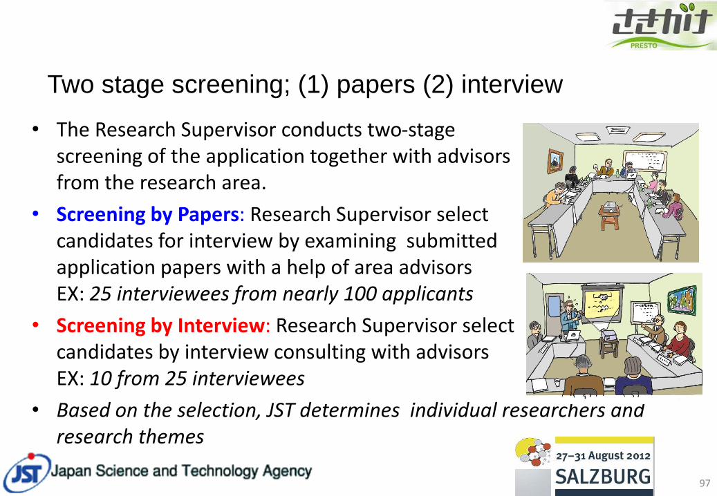
Two stage screening; (1) papers (2) interview
• The Research Supervisor conducts two-stage screening of the application together with advisors from the research area.
• Screening by Papers: Research Supervisor select candidates for interview by examining submitted application papers with a help of area advisors EX: 25 interviewees from nearly 100 applicants
• Screening by Interview: Research Supervisor select candidates by interview consulting with advisors EX: 10 from 25 interviewees
• Based on the selection, JST determines individual researchers and research themes
97

Organization
Suprevisor
Advisors
33 Researchers
stage (1): 11, stage (2): 10, stage (3): 12
JST Staffs
Office
Research Manager
Administrative Manager
98

99
“Site-Visit” to individual researcher’s labs
• The Research Supervisor visits the laboratories of individual researcher’s affiliation and grasp research environment and explain to his or her boss about the mission of the Program and ask to allow to conduct an independent research. – This process has an indispensable importance for researcher to
conduct researches on a theme independent from the affiliation.
– Supervisor can conduct careful management in accordance with the situation of the researcher.

Research Area Meetings
• JST holds Research Meetings sponsored by the Supervisor twice a year to discuss the research plan, to report the progress or to promote communication among researches in the research area.
• Researchers are very much activated by joining the Meeting through severe discussion with Supervisor, Advisors and other researchers.
• These research meetings help researchers to build wide personal networks across the organization and position.
Active discussion among researchers
Discussion continues to late at night
Hot discussion among researchers, advisors and supervisor
100

101
Publicity of Achievements by JST staffs
• Dept. of Public Relations & Science Portal help Press Release – Press releases and press lecture of research achievements are conducted by
JST specialist of publicity.
– JST News, a monthly magazine, introduce the research outcomes
• Science Communication Center send introduction video to Web – Science News, a JST Web Animation Site dispatches the contents of
researches
Press Release
Web News

Project Flow • The phase I group: October 2007March 2011
• The phase II group: October 2008March 2012
• The phase III group: October 2009March 2013
Japan Science and Technology Agency
2008FY 2009FY 2010FY
2009FY 2010FY 2011FY
2010FY 2011FY 2012FY
2007FY
2008FY
2009FY
Phase 1
Phase 2
Phase 3
1st Mtg
2008.1
Hayama
2nd Mtg
2008.6
Awaji il.
2008.1 2009.1 2010.1 2011.1 2012.1 2013.1
3rd Mtg
2008.11
Tokyo
4th Mtg
2009.4
Sendai
Report Mtg (1) as JSAP Symposium
Mini
WS1
Total Evaluation
Evaluation(1)
Evaluation(2)
Final
Symposium
Mini
WS2
5th Mtg
2009.11
Tsukub
a
Mini
WS3
Mini
WS4
6th Mtg
2010.4
Fukuoka
7th Mtg
2011.1
Osaka
Mini
WS5
Report Mtg (2) as JSAP Symposium
Mini
WS6
Mini
WS7
Mini
WS8
10th Mtg
2012.5
Nagoya
9th Mtg
2011.10
Nara
8th Mtg
2011.5
Sapporo 11th Mtg
2013.1
Awaji ild
102
Now we are in the final stage!

103
PRESTO is a unique virtual laboratory to promote young researchers
• Individual Research Themes independent from affiliation
• Reasonable amount of budget
• Flexible managements of research fund
• Acceleration of research by leadership of Supervisor
• Management such as Research Meetings, Site-Visits as Virtual Institute
• Support by Research Office:Research Administrators
• Recommendation to Awards
• Confidence and Aggressive Minds by stimulation by Colleagues
• Interdisciplinary relationship to build wide personal networks across the organization and position.

THANK YOU FOR YOUR ATTENTION

APPENDIX

106
Cabinet Office
Promotion System of S &T Policy in Japan
Prime Minister
Council for Science & Technology Policy(CSTP)
Consultation Response Opinion
Relevant Ministries and Agencies
Opinion
Member: - Prime Minister (Chair) - 6 Ministers - 8 Executive members - Academia: 6 - Industry: 2
Consultation Response
・Internal Affairs and Communications (IAC) ・ Education, Culture, Sports, S&T (MEXT) ・Health, Labor and Welfare (MOH) ・ Agriculture, Forestry and Fisheries (MAFF) ・Economy, Trade and Industry (METI) ・Land, Infrastructure and Transport (MLIT) ・Environment (MOE)
Mission: 1) Investigations and deliberations on basic
policies of S&T 2) Investigations and deliberations on the
resource allocation in S&T policy 3) Evaluations of nationally important R&D

107
Total S&T budget Total S&T Budget
1,000
0
4,000 4,584.1 4,358.1
4,049.0 4,084.1 4,040.4 4,140.1
3,511.3 3,468.5 3,544.4 3,597.4 3,608.4 3,577.9 3,574.3
(1,112.4) (1,183.2) (1,229.8) (1,284.1) (1,317.0) (1,331.2) (1,347.7)
3,570.8
4,044.7
(1,362.8)
4,240.5
(1,377.7)
3,563.9
429.7
240.0
5,046.3
1,097.0
(1,333.4)
3,589.0
385.3
4,189.6
402.8
3,665.2
(1,335.2)
197.8
3,669.5
(1,294.3) (1,359.0)
519.7
450.5
4,635.4
2nd Basic Plan 3rd Basic Plan 4th Basic Plan
(Billion yen)
FY2001
Japanese Government S&T Budget
Initial budget S&T promotion expenditures
(as part of initial budgets) Supplementary budget
Spending of local
public entities
2002 2003 2004 2005 2006 2008 2007 2009 2010 2011 2012
S&T promotion budget

108
Strategic Sector (Target of Research)
• Center of R&D Strategy (CRDS), a think-tank of JST, works out proposals through survey S&T fields, by drawing "bird's-eye view maps", and by listing up important R&D subjects →MEXT designates Strategic Sectors using the proposals as well as those from other government sections including those of CSTP
文科省 CRDS
CSTP
Strategic Sectors Bird’s eye Workshop
CSTP: counsel of Science and
Technology Planning Government Sections
The intelligent
MEXT

109
Research Areas
based on the Strategic Sector
• Based on strategic sectors, JST establishes research areas.
My case: Strategic Sector is “R & D for beyond-CMOS Devices” Designated Project Name is “Materials and Processes for Next-Generation Innovative Devices”
MEXT
Strategic Sectors
JST Office of Basic Research
PD Meeting

Research Office
• Research offices are established for each research area and take daily care of researches under the guidance of Supervisors.
• Research managers (who coordinate the research, determine research progress and give support for presentations), administrative managers (who purchase equipment and materials and deal with procedures for business trips) and office staffs are stationed in all research offices.
110


![Jst Bst: [Portfolio]](https://img.pdfslide.us/doc/110x75/55a446251a28abf32b8b46f8/jst-bst-portfolio-55a5186eb3369.jpg)
![Jst bst [portfolio]](https://img.pdfslide.us/doc/110x75/547b8193b4af9fda158b4ed4/jst-bst-portfolio.jpg)