Embed Size (px)
Citation preview
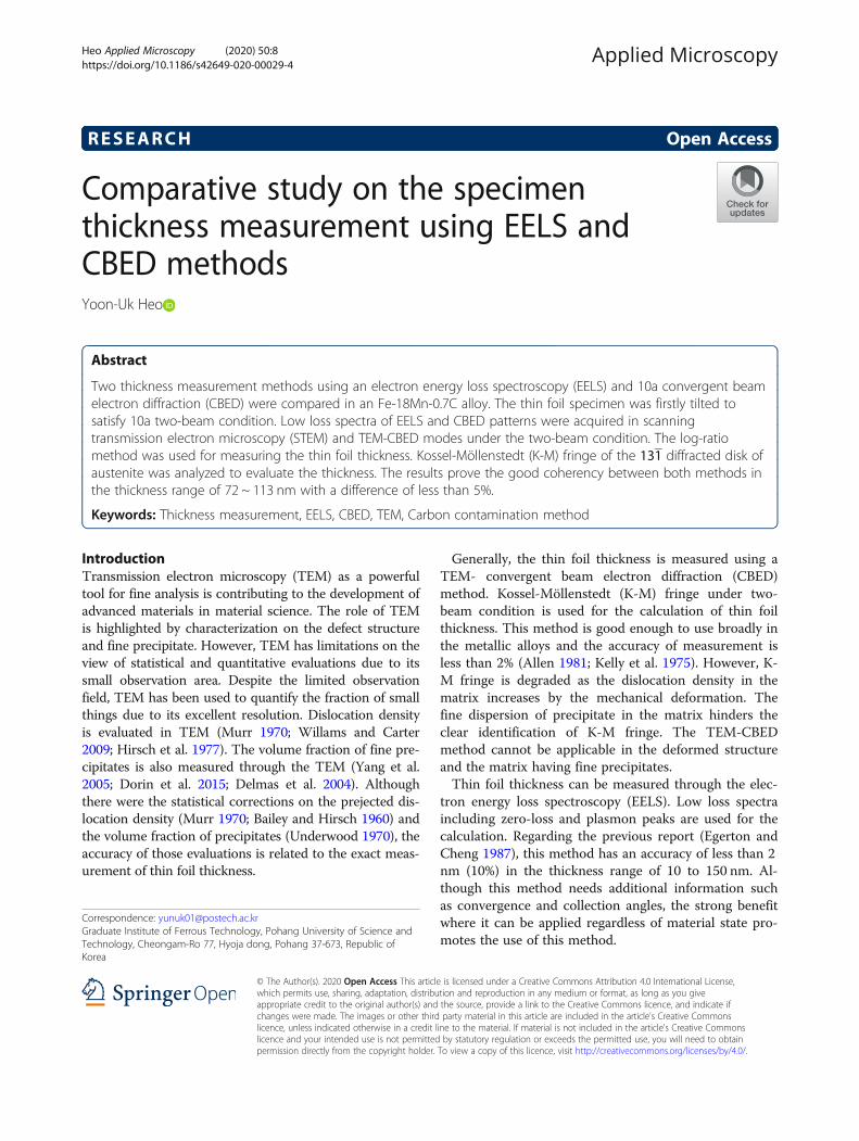
RESEARCH Open Access
Comparative study on the specimenthickness measurement using EELS andCBED methodsYoon-Uk Heo
Abstract
Two thickness measurement methods using an electron energy loss spectroscopy (EELS) and 10a convergent beamelectron diffraction (CBED) were compared in an Fe-18Mn-0.7C alloy. The thin foil specimen was firstly tilted tosatisfy 10a two-beam condition. Low loss spectra of EELS and CBED patterns were acquired in scanningtransmission electron microscopy (STEM) and TEM-CBED modes under the two-beam condition. The log-ratiomethod was used for measuring the thin foil thickness. Kossel-Möllenstedt (K-M) fringe of the 131 diffracted disk ofaustenite was analyzed to evaluate the thickness. The results prove the good coherency between both methods inthe thickness range of 72 ~ 113 nm with a difference of less than 5%.
Keywords: Thickness measurement, EELS, CBED, TEM, Carbon contamination method
IntroductionTransmission electron microscopy (TEM) as a powerfultool for fine analysis is contributing to the development ofadvanced materials in material science. The role of TEMis highlighted by characterization on the defect structureand fine precipitate. However, TEM has limitations on theview of statistical and quantitative evaluations due to itssmall observation area. Despite the limited observationfield, TEM has been used to quantify the fraction of smallthings due to its excellent resolution. Dislocation densityis evaluated in TEM (Murr 1970; Willams and Carter2009; Hirsch et al. 1977). The volume fraction of fine pre-cipitates is also measured through the TEM (Yang et al.2005; Dorin et al. 2015; Delmas et al. 2004). Althoughthere were the statistical corrections on the prejected dis-location density (Murr 1970; Bailey and Hirsch 1960) andthe volume fraction of precipitates (Underwood 1970), theaccuracy of those evaluations is related to the exact meas-urement of thin foil thickness.
Generally, the thin foil thickness is measured using aTEM- convergent beam electron diffraction (CBED)method. Kossel-Möllenstedt (K-M) fringe under two-beam condition is used for the calculation of thin foilthickness. This method is good enough to use broadly inthe metallic alloys and the accuracy of measurement isless than 2% (Allen 1981; Kelly et al. 1975). However, K-M fringe is degraded as the dislocation density in thematrix increases by the mechanical deformation. Thefine dispersion of precipitate in the matrix hinders theclear identification of K-M fringe. The TEM-CBEDmethod cannot be applicable in the deformed structureand the matrix having fine precipitates.Thin foil thickness can be measured through the elec-
tron energy loss spectroscopy (EELS). Low loss spectraincluding zero-loss and plasmon peaks are used for thecalculation. Regarding the previous report (Egerton andCheng 1987), this method has an accuracy of less than 2nm (10%) in the thickness range of 10 to 150 nm. Al-though this method needs additional information suchas convergence and collection angles, the strong benefitwhere it can be applied regardless of material state pro-motes the use of this method.
© The Author(s). 2020 Open Access This article is licensed under a Creative Commons Attribution 4.0 International License,which permits use, sharing, adaptation, distribution and reproduction in any medium or format, as long as you giveappropriate credit to the original author(s) and the source, provide a link to the Creative Commons licence, and indicate ifchanges were made. The images or other third party material in this article are included in the article's Creative Commonslicence, unless indicated otherwise in a credit line to the material. If material is not included in the article's Creative Commonslicence and your intended use is not permitted by statutory regulation or exceeds the permitted use, you will need to obtainpermission directly from the copyright holder. To view a copy of this licence, visit http://creativecommons.org/licenses/by/4.0/.
Correspondence: [email protected] Institute of Ferrous Technology, Pohang University of Science andTechnology, Cheongam-Ro 77, Hyoja dong, Pohang 37-673, Republic ofKorea
Applied MicroscopyHeo Applied Microscopy (2020) 50:8 https://doi.org/10.1186/s42649-020-00029-4

In this study, we aim the reassessment of the relative ac-curacy of the EELS thickness measurement method for fu-ture applications in the deformed metallic materials orfine precipitate-bearing materials. The observed results ofEELS and CBED at the coincident positions in an Fe-18Mn-0.7C alloy are compared and further discussed.
Material and methodsSpecimen preparation and characterizationThe ingot of an Fe-18Mn-0.7C alloy was prepared byvacuum induction melting and subsequently hot-rolledto 4 mm thickness. Annealing treatment was performedat 850 °C for 10 min after cold-rolling of 50%. TEM spe-cimen was prepared by electrochemical polishing in asolution of 12 pct perchloric acid + 90 pct acetic acid atroom temperature after mechanical thinning to 100 μmthickness. Final Ar+ ion milling was conducted to re-move the etching effect formed at the electrochemicalpolishing using a precision ion-polishing system (PIPS,GATAN 691, New York, USA) with the acceleratingvoltage of 1.0 keV for 20 min. The specimen was ob-served in a JEOL 200 kV field-emission transmissionelectron microscope (JEM-2100F) equipped with a Gatan776 EELS spectrometer (Enfina 1000) under the acceler-ating voltage of 200 keV.
Results and discussionThickness measurement using TEM-CBED methodFollowing the dynamical theory of diffraction contrast,the amplitude of the diffracted wave (ϕg) and the speci-men thickness (t) have the following relationship (Will-ams and Carter 2009; Hirsch et al. 1977);
ϕ2g ¼
πξg
� �2 sin2πtseffπtseff
ð1Þ
where ξg is the extinction distance of material and theeffective deviation vector seff has the relation of seff
¼ffiffiffiffiffiffiffiffiffiffiffiffiffiffiffiffiffiffiffis2 þ 1=ξ2g
q. Equation (1) shows also the relation be-
tween a deviation vector and a contrast of the image atthe constant thickness. A representative case of that isthe contrast modulation in a CBED disk. Figure 1(a) is atypical K-M fringe under the two-beam condition. Theintensity minima in the K-M fringe of the diffracted hklCBED disk can be obtained when ϕg = 0. On the otherhand, a deviation vector si for ith fringe in a diffracteddisk has following relationship (Willams and Carter2009; Hirsch et al. 1977);
si ¼ λ
d2hkl
!Δθi2θB
� �ð2Þ
where λ is a wavelength of the electron, dhkl is an inter-planar distance of hkl plane, and θB is the Bragg anglefor hkl plane. Combining equation (1) and (2) and apply-ing ϕg = 0 condition (t × seff = ni, ni is an integer), we canobtain the following equation;
s2in2i
¼ −1
ξ2g∙1n2i
þ 1t2: ð3Þ
Referring equation (3), we can obtain the specimen
thickness using the intercept value in a s2in2i
vs. 1n2i
plot
(Fig. 1(b)).
Fig. 1 a A typical K-M fringe under the two-beam condition and b a plot which shows a linear relationship between (si/ni)2 and 1/ni
2
Heo Applied Microscopy (2020) 50:8 Page 2 of 7

To obtain the K-M fringe, the specimen tilted to the[013] on-axis condition. Bright field (BF) – TEM imageand corresponding electron diffraction pattern areshown in Figs. 2(a) and (b). The specimen was tiltedfrom the on-axis condition to obtain a two-beam condi-tion. 000 and 131 spots show a strong intensity in theobtained two-beam condition (Fig. 2(c)). K-M fringeswere obtained at the positions 1 to 5 in Fig. 2(a) asshown in Figs. 3(a) to (e). The specimen thicknesseswere calculated by equation (3). Specimen thicknessesshow maximum at the position 4 and minimum at pos-ition 1 in the range of 72 ~ 113 nm.
Thickness measurement using EELS spectraThree different methods (log-ratio method, Bethe sumrule, and Kramers-Kronig sum rule) for the measure-ment of thickness using an EELS spectrum were intro-duced in the previous reports (Egerton and Cheng 1987;Egerton 1996). Among them, the current study used thelog-ratio method.Figure 4(a) shows a representative low-loss EELS
spectrum. The low-loss spectrum includes zero loss (I0)and plasmon loss (Ip) peaks. Specimen thickness is obtainedby the following formula (Egerton and Cheng 1987);
t ¼ ΛlnItI0
ð4Þ
where Λ is the average mean free path for inelastic scat-tering of electron and It is the total integration of EELSspectra. Λ can be obtained from the following relations;
Λ nmð Þ ¼106F
E0
Em
� �
ln2E0βEm
� � ; F ¼ 1þ E0=1022
1þ E0511
� �2 ;Em ¼ 7:6Z0:36
ð5Þwhere F is a relativistic factor, β is the collection semi-
angle in mrad, and E0 is the incident energy in keV. F, β,and E0 in the current experimental condition are 0.618,1.3 mrad, and 200 keV, respectively. In the alloy system,atomic number is replaced to the effective atomic number(Zeff) which can be obtained by the following formula;
Zeff ¼P
i f iZ1:3iP
i f iZ0:3i
ð6Þ
where fi is the atomic fraction of each element whichhas atomic number Zi. Zeff
is calculated to 25.4 in the Fe-18Mn-0.7C alloy. Thethickness of the specimen calculated from low-loss EELspectra after removing plural scattering (Fig. 4(b)) byFourier-log deconvolution (Egerton 1996).Figure 5(a) and (b) are BF- and high angle annular
dark field (HAADF)- scanning TEM (STEM) images inthe same area where thicknesses were measured by theTEM-CBED method. The observation is performedunder the coincident condition without any tilting of thespecimen. Therefore, the measured thickness from theEEL spectrum can be directly compared. The positions(1 ~ 5) in Fig. 5(a) and (b) correspond to the same posi-tions in Fig. 2(a). The obtained low-loss spectra in posi-tions 1 to 5 are displayed in Fig. 5(c) to (g). Applying theexperimental parameters which are explained above, wecalculate specimen thicknesses at each position using asoftware (Digital Micrograph 1.8, Gatan Inc., New York,USA). The calculated thicknesses show a similar ten-dency with those in the CBED method (Fig. 3(a) to (e));maximum thickness is 111.8 nm in position 4 and mini-mum thickness is 72.2 nm in position 1.
Comparison of TEM-CBED and EELS methodsThe obtained thicknesses using TEM-CBED and EELSmethods are shown together in Fig. 6(a). Bothmethods reflect well the local thickness variation suchas a gradual increase from position 1 to position 4
Fig. 2 a BF-TEM image and b corresponding electron diffraction pattern, and c the obtained two-beam spot
Heo Applied Microscopy (2020) 50:8 Page 3 of 7
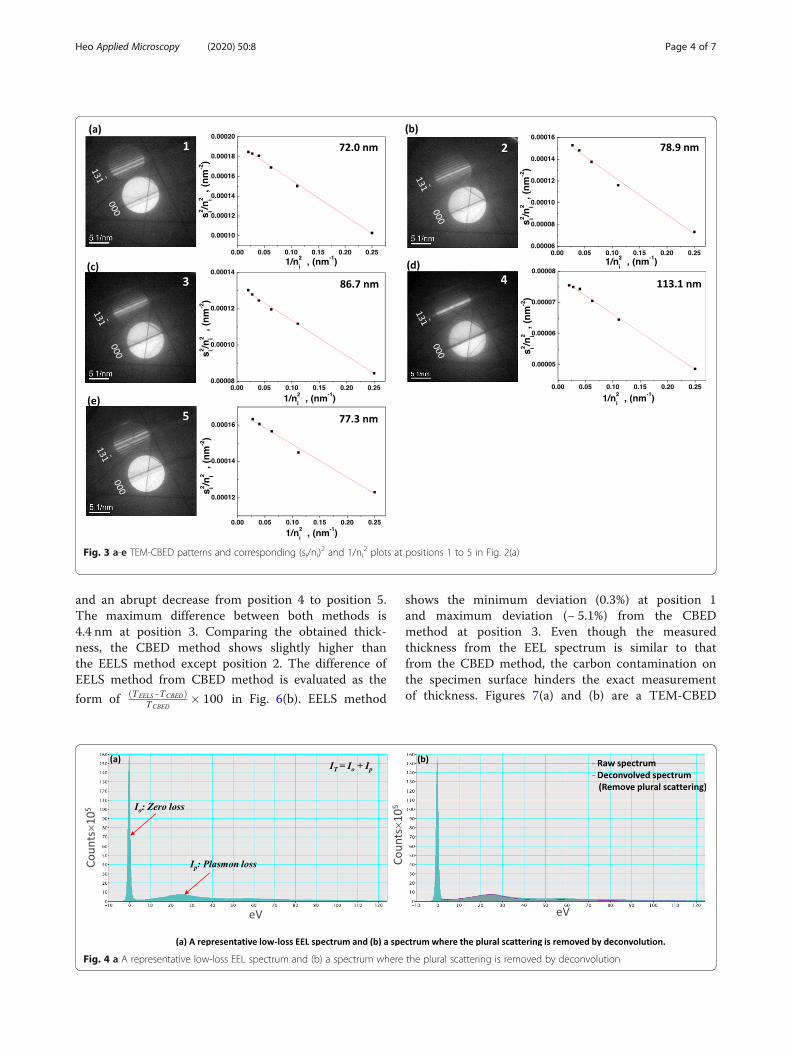
and an abrupt decrease from position 4 to position 5.The maximum difference between both methods is4.4 nm at position 3. Comparing the obtained thick-ness, the CBED method shows slightly higher thanthe EELS method except position 2. The difference ofEELS method from CBED method is evaluated as the
form of ðTEELS−TCBEDÞTCBED
� 100 in Fig. 6(b). EELS method
shows the minimum deviation (0.3%) at position 1and maximum deviation (− 5.1%) from the CBEDmethod at position 3. Even though the measuredthickness from the EEL spectrum is similar to thatfrom the CBED method, the carbon contamination onthe specimen surface hinders the exact measurementof thickness. Figures 7(a) and (b) are a TEM-CBED
Fig. 3 a-e TEM-CBED patterns and corresponding (si/ni)2 and 1/ni
2 plots at positions 1 to 5 in Fig. 2(a)
Fig. 4 a A representative low-loss EEL spectrum and (b) a spectrum where the plural scattering is removed by deconvolution
Heo Applied Microscopy (2020) 50:8 Page 4 of 7

pattern and a corresponding s2in2i
vs. 1n2i
plot. The mea-
sured thickness is 103.4 nm. EEL spectra were ob-tained after long exposure to make carboncontamination in the same position. The calculatedthicknesses increase from 139.8 to 154.1 nm as theacquisition time of EEL spectra is retarded (Fig. 7(d)
and (e)). These values are far from the CBED result.Caution on the carbon contamination is needed toprevent wrong evaluation when the EELS method is ap-plied for the specimen thickness measurement. To see thecarbon contamination, the specimen is tilted to 22.8°. Asshown in Fig. 7(c), the carbon contaminations on the topand bottom surfaces of the specimen are resolved by two
Fig. 5 (a) BF- and (b)ADF-STEM images at the same position in Fig. 2(a), and (b) to (g) low-loss EEL spectra at positions 1 ~ 5
Fig. 6 Comparison of the measured thickness; (a) thicknesses obtained from CBED and EELS, and (b) the difference of the EELS method from theCBED method
Heo Applied Microscopy (2020) 50:8 Page 5 of 7
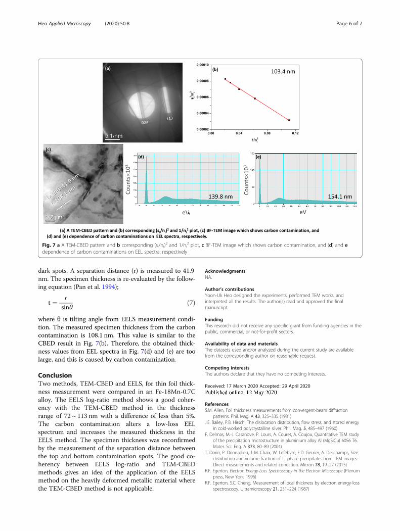
dark spots. A separation distance (r) is measured to 41.9nm. The specimen thickness is re-evaluated by the follow-ing equation (Pan et al. 1994);
t ¼ rsinθ
ð7Þ
where θ is tilting angle from EELS measurement condi-tion. The measured specimen thickness from the carboncontamination is 108.1 nm. This value is similar to theCBED result in Fig. 7(b). Therefore, the obtained thick-ness values from EEL spectra in Fig. 7(d) and (e) are toolarge, and this is caused by carbon contamination.
ConclusionTwo methods, TEM-CBED and EELS, for thin foil thick-ness measurement were compared in an Fe-18Mn-0.7Calloy. The EELS log-ratio method shows a good coher-ency with the TEM-CBED method in the thicknessrange of 72 ~ 113 nm with a difference of less than 5%.The carbon contamination alters a low-loss EELspectrum and increases the measured thickness in theEELS method. The specimen thickness was reconfirmedby the measurement of the separation distance betweenthe top and bottom contamination spots. The good co-herency between EELS log-ratio and TEM-CBEDmethods gives an idea of the application of the EELSmethod on the heavily deformed metallic material wherethe TEM-CBED method is not applicable.
AcknowledgmentsNA.
Author’s contributionsYoon-Uk Heo designed the experiments, performed TEM works, andinterpreted all the results. The author(s) read and approved the finalmanuscript.
FundingThis research did not receive any specific grant from funding agencies in thepublic, commercial, or not-for-profit sectors.
Availability of data and materialsThe datasets used and/or analyzed during the current study are availablefrom the corresponding author on reasonable request.
Competing interestsThe authors declare that they have no competing interests.
Received: 17 March 2020 Accepted: 29 April 2020
ReferencesS.M. Allen, Foil thickness measurements from convergent-beam diffraction
patterns. Phil. Mag. A 43, 325–335 (1981)J.E. Bailey, P.B. Hirsch, The dislocation distribution, flow stress, and stored energy
in cold-worked polycrystalline silver. Phil. Mag. 5, 485–497 (1960)F. Delmas, M.-J. Casanove, P. Lours, A. Couret, A. Coujou, Quantitative TEM study
of the precipitation microstructure in aluminium alloy Al (MgSiCu) 6056 T6.Mater. Sci. Eng. A 373, 80–89 (2004)
T. Dorin, P. Donnadieu, J.-M. Chaix, W. Lefebvre, F.D. Geuser, A. Deschamps, Sizedistribution and volume fraction of T1 phase precipitates from TEM images:Direct measurements and related correction. Micron 78, 19–27 (2015)
R.F. Egerton, Electron Energy-Loss Spectroscopy in the Electron Microscope (Plenumpress, New York, 1996)
R.F. Egerton, S.C. Cheng, Measurement of local thickness by electron energy-lossspectroscopy. Ultramicroscopy 21, 231–224 (1987)
Fig. 7 a A TEM-CBED pattern and b corresponding (si/ni)2 and 1/ni
2 plot, c BF-TEM image which shows carbon contamination, and (d) and edependence of carbon contaminations on EEL spectra, respectively
Heo Applied Microscopy (2020) 50:8 Page 6 of 7
P. Hirsch, A. Howie, R.B. Nicholson, D.W. Pashley, M.J. Whelan, Electron Microscopyof Thin Crystals (Robert E. Krieger Pub. Comp, Huntington, 1977)
P.M. Kelly, A. Jostsons, R.G. Blake, J.G. Napier, The determination of foil thicknessby scanning transmission electron microscopy. Phys. Status Solidi 31, 771–780 (1975)
L.E. Murr, Electron Optical Applications in Materials Science (McGraw-Hill BookComp, New York, 1970)
Z. Pan, C.K.L. Davies, R.N. Stevens, Measurement of foil thickness in transmissionelectron microscopy. J. Mater. Sci. 29, 1920–1924 (1994)
E.E. Underwood, Quantitative stereology (Addison-Wesley Publishing Comp,Massachusetts, 1970)
D.B. Willams, C.B. Carter, Transmission Electron Microscopy, 2nd edn. (Springer,New York, 2009)
Z. Yang, W. Tirry, D. Schryvers, Analytical TEM investigations on concentrationgradients surrounding Ni4Ti3 precipitates in Ni-Ti shape memory material.Scripta Mater. 52, 1129–1134 (2005)
Publisher’s NoteSpringer Nature remains neutral with regard to jurisdictional claims inpublished maps and institutional affiliations.
Heo Applied Microscopy (2020) 50:8 Page 7 of 7