Embed Size (px)
Citation preview
Comparative Analysis of Practical ThresholdVoltage Extraction Techniques for CMOSand LDMOS Devices in 180 nm Technology
Yu-Hsing Cheng
ON Semiconductor
October 15, 2018
2
Outline
Overview and Background
MOSFET Device Id-Vg Characteristics and Threshold Voltage
Threshold Voltage Extraction Techniques
Comparison of Threshold Voltage Extraction Results
Summary and Conclusion

Overview and Background
4
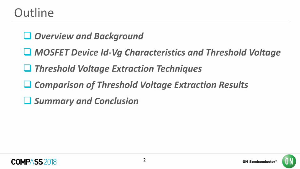
Technology Trends : Moore’s Law and More
Sample title (First Level)
Sample Description Text (second Level)
• Sample Bullet (third level)
– Sample Bullet 2 (fourth level)
o Sample Bullet 3 (fifth level)
Guo Qi Zhang, Alfred Roosmalen, “The Changing Landscape of Micro/Nanoelectronics”, in More than Moore: Creating High Value Micro/Nanoelectronics, Springer, 2009.
• The first transistor was invented in 1947 (announced in 1948).
• The first IC was constructed in 1958.
• Gordon Moore first published his observation and prediction in 1965.
• It has become a self-fulfilling prophecy and a yardstick for technology progress.
• More-than-Moore refers to non-digital functionalities not scaling at the rate of Moore’s Law.
• Trending: Smart manufacturing, virtual metrology, heterogeneous integration…
5
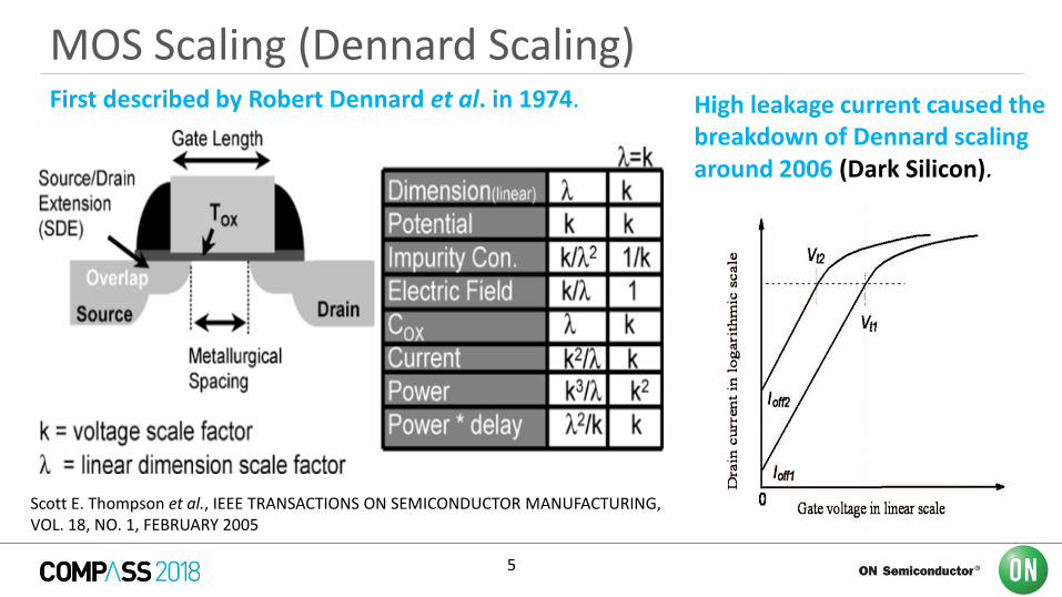
MOS Scaling (Dennard Scaling)
Scott E. Thompson et al., IEEE TRANSACTIONS ON SEMICONDUCTOR MANUFACTURING, VOL. 18, NO. 1, FEBRUARY 2005
First described by Robert Dennard et al. in 1974. High leakage current caused the breakdown of Dennard scaling around 2006 (Dark Silicon).
6
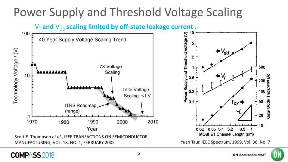
Power Supply and Threshold Voltage Scaling
Scott E. Thompson et al., IEEE TRANSACTIONS ON SEMICONDUCTOR MANUFACTURING, VOL. 18, NO. 1, FEBRUARY 2005 Yuan Taur, IEEE Spectrum, 1999, Vol. 36, No. 7
VT and VDD scaling limited by off-state leakage current .
7
Driving Energy Efficient Innovations
Analog Solutions Group Power Solutions Group Intelligent Sensing Group
MOSFET Device Id-Vg Characteristics and VT
9
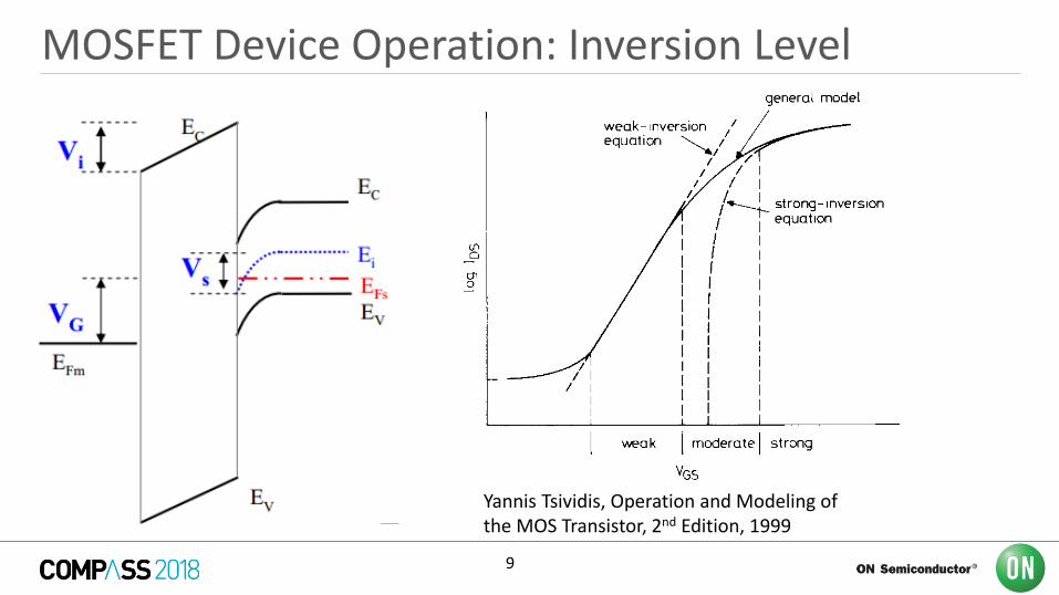
MOSFET Device Operation: Inversion Level
Yannis Tsividis, Operation and Modeling of the MOS Transistor, 2nd Edition, 1999
10
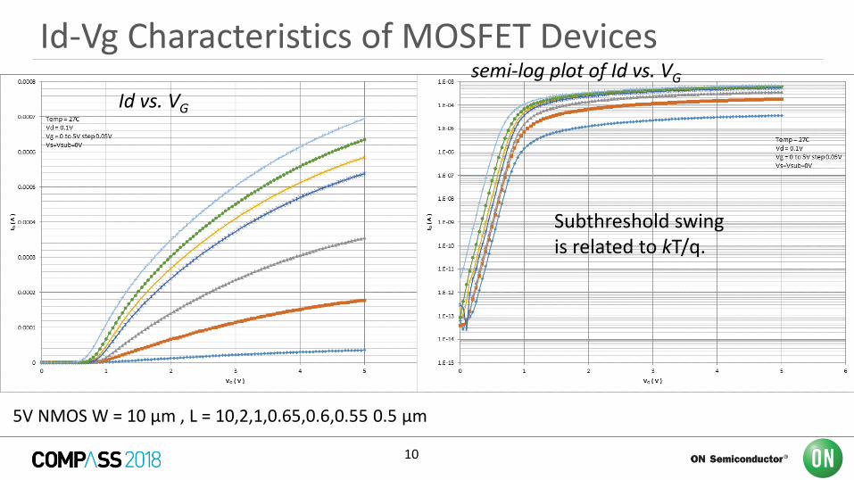
Id-Vg Characteristics of MOSFET Devices
Sample title (First Level)
Sample Description Text (second Level)
• Sample Bullet (third level)
– Sample Bullet 2 (fourth level)
o Sample Bullet 3 (fifth level) Subthreshold swing is related to kT/q.
5V NMOS W = 10 µm , L = 10,2,1,0.65,0.6,0.55 0.5 µm
Id vs. VG
semi-log plot of Id vs. VG
11
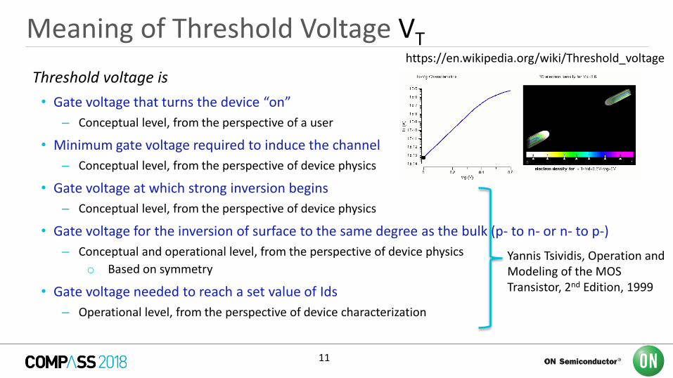
Meaning of Threshold Voltage VT
Threshold voltage is
• Gate voltage that turns the device “on”
– Conceptual level, from the perspective of a user
• Minimum gate voltage required to induce the channel
– Conceptual level, from the perspective of device physics
• Gate voltage at which strong inversion begins
– Conceptual level, from the perspective of device physics
• Gate voltage for the inversion of surface to the same degree as the bulk (p- to n- or n- to p-)
– Conceptual and operational level, from the perspective of device physics
o Based on symmetry
• Gate voltage needed to reach a set value of Ids
– Operational level, from the perspective of device characterization
Yannis Tsividis, Operation and Modeling of the MOS Transistor, 2nd Edition, 1999
https://en.wikipedia.org/wiki/Threshold_voltage
12
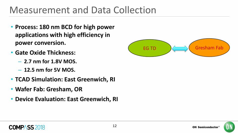
Measurement and Data Collection
• Process: 180 nm BCD for high power applications with high efficiency in power conversion.
• Gate Oxide Thickness:
– 2.7 nm for 1.8V MOS.
– 12.5 nm for 5V MOS.
• TCAD Simulation: East Greenwich, RI
• Wafer Fab: Gresham, OR
• Device Evaluation: East Greenwich, RI
EG TD Gresham Fab
13
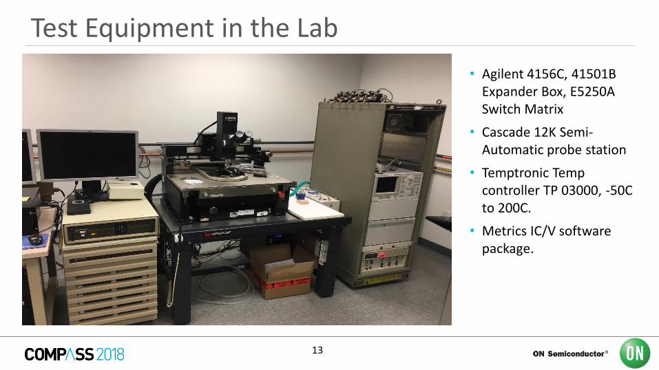
Test Equipment in the Lab
• Agilent 4156C, 41501B Expander Box, E5250A Switch Matrix
• Cascade 12K Semi-Automatic probe station
• Temptronic Temp controller TP 03000, -50C to 200C.
• Metrics IC/V software package.
14
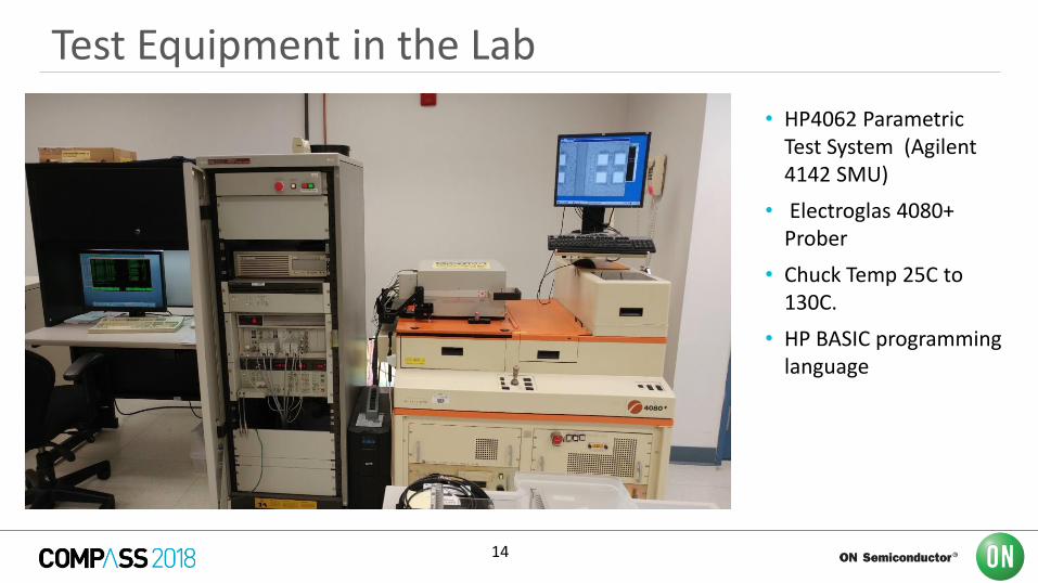
Test Equipment in the Lab
• HP4062 Parametric Test System (Agilent 4142 SMU)
• Electroglas 4080+ Prober
• Chuck Temp 25C to 130C.
• HP BASIC programming language
Threshold Voltage Extraction Techniques
16
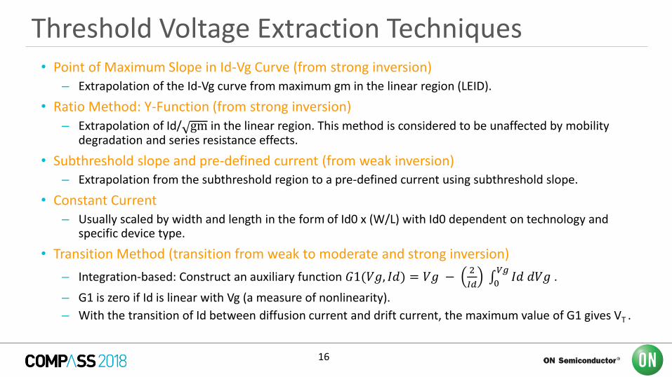
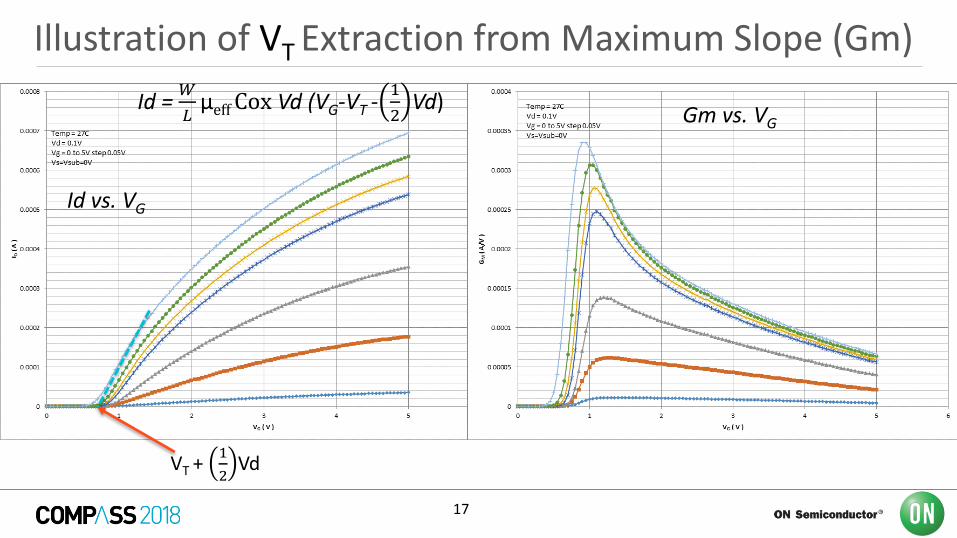
Threshold Voltage Extraction Techniques• Point of Maximum Slope in Id-Vg Curve (from strong inversion)
– Extrapolation of the Id-Vg curve from maximum gm in the linear region (LEID).
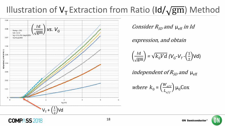
• Ratio Method: Y-Function (from strong inversion)– Extrapolation of Id/ gm in the linear region. This method is considered to be unaffected by mobility
degradation and series resistance effects.
• Subthreshold slope and pre-defined current (from weak inversion)– Extrapolation from the subthreshold region to a pre-defined current using subthreshold slope.
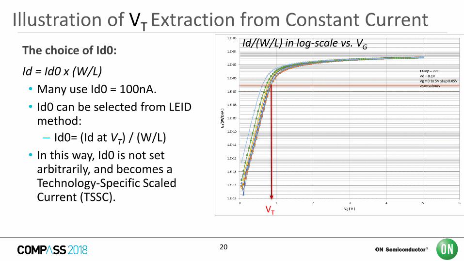
• Constant Current– Usually scaled by width and length in the form of Id0 x (W/L) with Id0 dependent on technology and
specific device type.
• Transition Method (transition from weak to moderate and strong inversion)
– Integration-based: Construct an auxiliary function 𝐺1(𝑉𝑔, 𝐼𝑑) = 𝑉𝑔 −2
𝐼𝑑 0𝑉𝑔𝐼𝑑 𝑑𝑉𝑔 .
– G1 is zero if Id is linear with Vg (a measure of nonlinearity).
– With the transition of Id between diffusion current and drift current, the maximum value of G1 gives VT .
17
Illustration of VT Extraction from Maximum Slope (Gm)
Sample title (First Level)
Sample Description Text (second Level)
• Sample Bullet (third level)
– Sample Bullet 2 (fourth level)
o Sample Bullet 3 (fifth level)
VT + 1
2Vd
Gm vs. VG
Id vs. VG
Id = 𝑊
𝐿µeffCox Vd (VG-VT -
1
2Vd)
18
Illustration of VT Extraction from Ratio (Id/ gm) Method
Sample title (First Level)
Sample Description Text (second Level)
• Sample Bullet (third level)
– Sample Bullet 2 (fourth level)
o Sample Bullet 3 (fifth level)
𝐼𝑑
gmvs. VG
VT + 1
2Vd
Consider RSD and µeff in Id
expression, and obtain
𝐼𝑑
gm= 𝑘0𝑉𝑑 (VG-VT -
1
2Vd)
independent of RSD and µeff
where 𝑘0 =𝑊
𝑒𝑓𝑓
𝐿𝑒𝑓𝑓
µ0Cox
19
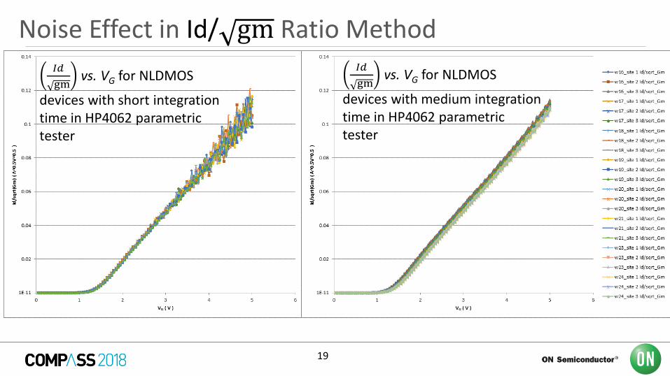
Noise Effect in Id/ gm Ratio Method
Sample title (First Level)
Sample Description Text (second Level)
• Sample Bullet (third level)
– Sample Bullet 2 (fourth level)
o Sample Bullet 3 (fifth level)
𝐼𝑑
gmvs. VG for NLDMOS
devices with medium integration time in HP4062 parametric tester
𝐼𝑑
gmvs. VG for NLDMOS
devices with short integration time in HP4062 parametric tester
20
Illustration of VT Extraction from Constant Current
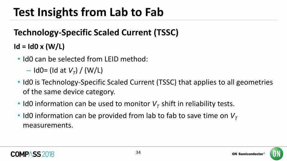
The choice of Id0:
Id = Id0 x (W/L)
• Many use Id0 = 100nA.
• Id0 can be selected from LEID method:
– Id0= (Id at VT) / (W/L)
• In this way, Id0 is not set arbitrarily, and becomes a Technology-Specific Scaled Current (TSSC).
Id/(W/L) in log-scale vs. VG
VT
21
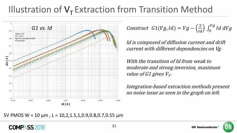
Illustration of VT Extraction from Transition Method
Sample title (First Level)
Sample Description Text (second Level)
• Sample Bullet (third level)
– Sample Bullet 2 (fourth level)
o Sample Bullet 3 (fifth level)
Construct 𝐺1(𝑉𝑔, 𝐼𝑑) = 𝑉𝑔 −2
𝐼𝑑 0𝑉𝑔𝐼𝑑 𝑑𝑉𝑔
Id is composed of diffusion current and drift current with different dependencies on Vg.
With the transition of Id from weak to moderate and strong inversion, maximum value of G1 gives VT .
Integration-based extraction methods present no noise issue as seen in the graph on left.
5V PMOS W = 10 µm , L = 10,2,1.5,1,0.9,0.8,0.7,0.55 µm
G1 vs. Id
22
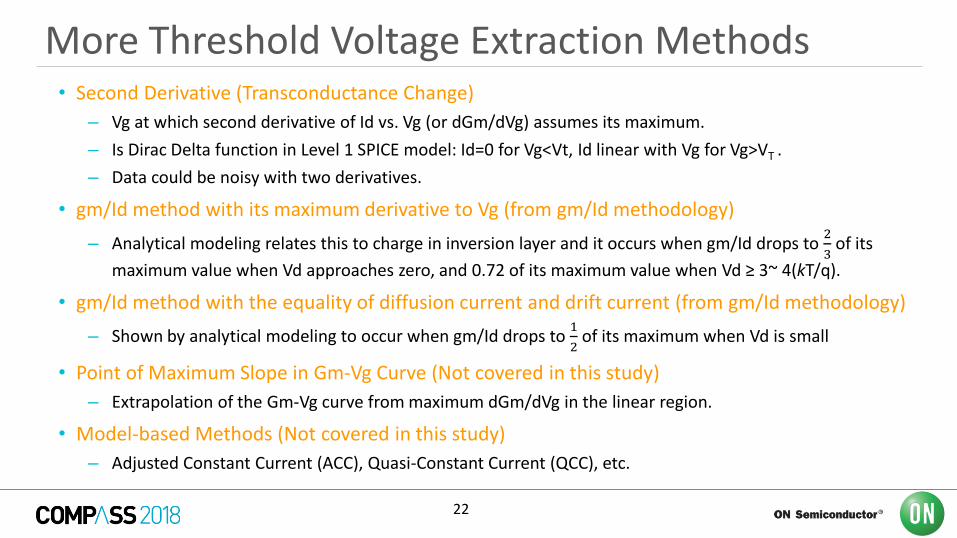
More Threshold Voltage Extraction Methods• Second Derivative (Transconductance Change)
– Vg at which second derivative of Id vs. Vg (or dGm/dVg) assumes its maximum.
– Is Dirac Delta function in Level 1 SPICE model: Id=0 for Vg<Vt, Id linear with Vg for Vg>VT .
– Data could be noisy with two derivatives.
• gm/Id method with its maximum derivative to Vg (from gm/Id methodology)
– Analytical modeling relates this to charge in inversion layer and it occurs when gm/Id drops to 2
3of its
maximum value when Vd approaches zero, and 0.72 of its maximum value when Vd ≥ 3~ 4(kT/q).
• gm/Id method with the equality of diffusion current and drift current (from gm/Id methodology)
– Shown by analytical modeling to occur when gm/Id drops to 1
2of its maximum when Vd is small
• Point of Maximum Slope in Gm-Vg Curve (Not covered in this study)
– Extrapolation of the Gm-Vg curve from maximum dGm/dVg in the linear region.
• Model-based Methods (Not covered in this study)
– Adjusted Constant Current (ACC), Quasi-Constant Current (QCC), etc.
23
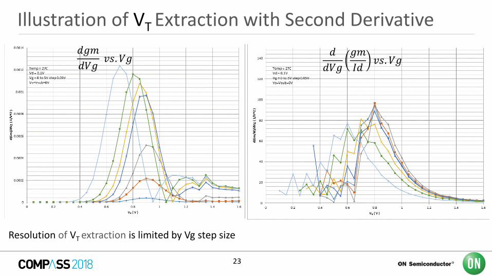
Illustration of VT Extraction with Second Derivative
Sample title (First Level)
Sample Description Text (second Level)
• Sample Bullet (third level)
– Sample Bullet 2 (fourth level)
o Sample Bullet 3 (fifth level)
𝑑
𝑑𝑉𝑔
𝑔𝑚
𝐼𝑑𝑣𝑠. 𝑉𝑔
𝑑𝑔𝑚
𝑑𝑉𝑔𝑣𝑠. 𝑉𝑔
Resolution of VT extraction is limited by Vg step size
24
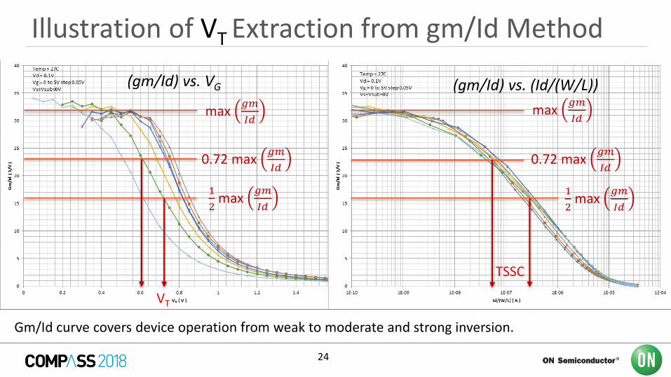
Illustration of VT Extraction from gm/Id Method
Sample title (First Level)
Sample Description Text (second Level)
• Sample Bullet (third level)
– Sample Bullet 2 (fourth level)
o Sample Bullet 3 (fifth level)
(gm/Id) vs. VG (gm/Id) vs. (Id/(W/L))
max 𝑔𝑚
𝐼𝑑max
𝑔𝑚
𝐼𝑑
0.72 max 𝑔𝑚
𝐼𝑑0.72 max
𝑔𝑚
𝐼𝑑
1
2max
𝑔𝑚
𝐼𝑑
1
2max
𝑔𝑚
𝐼𝑑
VT
TSSC
Gm/Id curve covers device operation from weak to moderate and strong inversion.
Comparison of VT Extraction Results
26
Comparison of VT Extraction Results
Sample title (First Level)
Sample Description Text (second Level)
• Sample Bullet (third level)
– Sample Bullet 2 (fourth level)
o Sample Bullet 3 (fifth level)
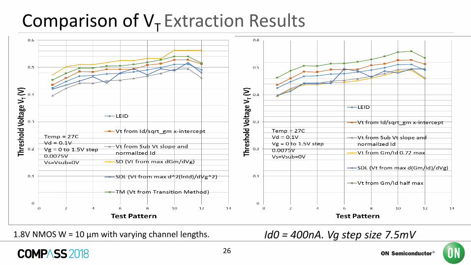
1.8V NMOS W = 10 µm with varying channel lengths. Id0 = 400nA. Vg step size 7.5mV
27
Comparison of VT Extraction Results
Sample title (First Level)
Sample Description Text (second Level)
• Sample Bullet (third level)
– Sample Bullet 2 (fourth level)
o Sample Bullet 3 (fifth level)
Id0 = 400nA. Vg step size 7.5mV
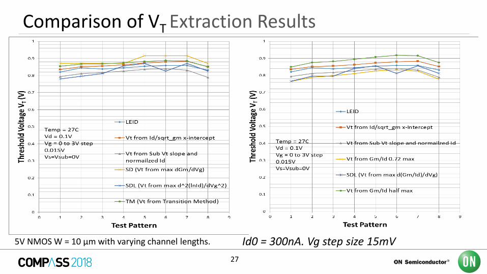
Id0 = 300nA. Vg step size 15mV5V NMOS W = 10 µm with varying channel lengths.
28
Comparison of VT Extraction Results for LDMOS
Sample title (First Level)
Sample Description Text (second Level)
• Sample Bullet (third level)
– Sample Bullet 2 (fourth level)
o Sample Bullet 3 (fifth level)
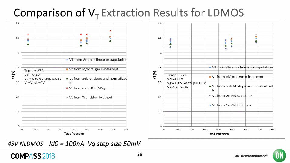
45V NLDMOS Id0 = 100nA. Vg step size 50mV
29
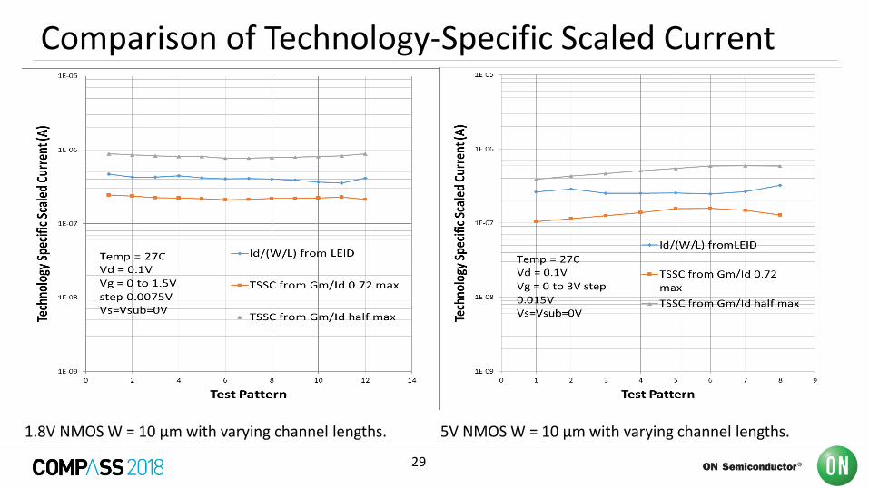
Comparison of Technology-Specific Scaled Current
Sample title (First Level)
Sample Description Text (second Level)
• Sample Bullet (third level)
– Sample Bullet 2 (fourth level)
o Sample Bullet 3 (fifth level)
1.8V NMOS W = 10 µm with varying channel lengths. 5V NMOS W = 10 µm with varying channel lengths.
30
Discussion of VT Extraction Results
• Id/ gm ratio (Y-Function) method and transition method both produce VT extraction results in good agreement with VT from LEID method (slightly higher).
• VT extraction results from subthreshold slope and pre-defined Id is consistent with VT
from LEID method (slightly lower). This method is valid only when there is no deviation of subthreshold Id-Vg characteristics from a straight line in semi-log plot (so is the Match Point method in literature).
• Technology-Specific Scaled Current (TSSC) can be selected from Id at VT from LEID method for each device category (e.g., 1.8V NMOS, 5V NMOS or 45V NLDMOS).
• Second derivative method produces VT extraction results higher than VT from LEID method.
• Gm/Id curve covers device operation from weak to moderate and strong inversion. VT
from LEID method lies between the two predictions from gm/Id methodology.
31
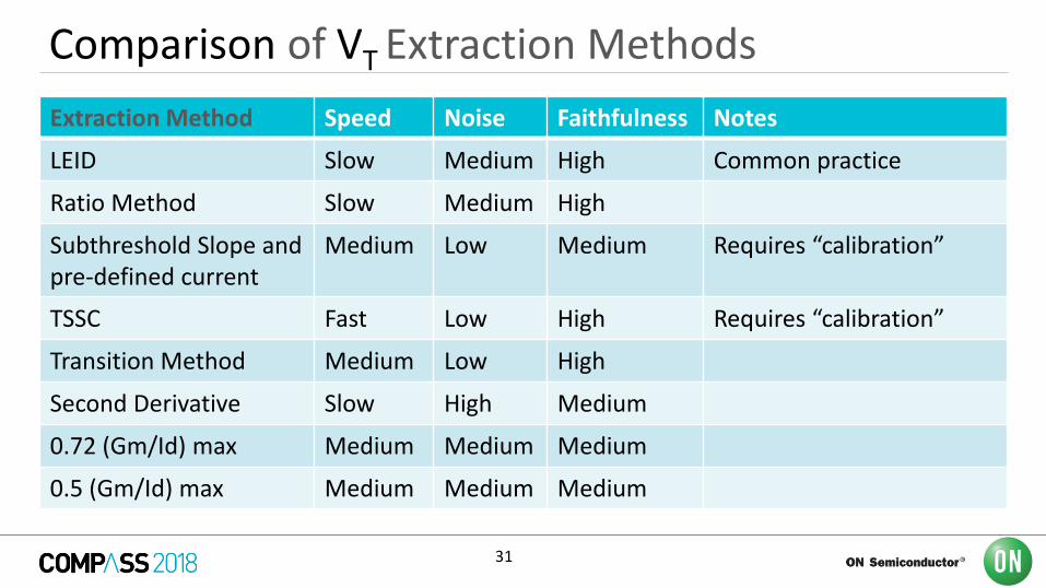
Comparison of VT Extraction Methods
Extraction Method Speed Noise Faithfulness Notes
LEID Slow Medium High Common practice
Ratio Method Slow Medium High
Subthreshold Slope and pre-defined current
Medium Low Medium Requires “calibration”
TSSC Fast Low High Requires “calibration”
Transition Method Medium Low High
Second Derivative Slow High Medium
0.72 (Gm/Id) max Medium Medium Medium
0.5 (Gm/Id) max Medium Medium Medium
Summary and Conclusion
33
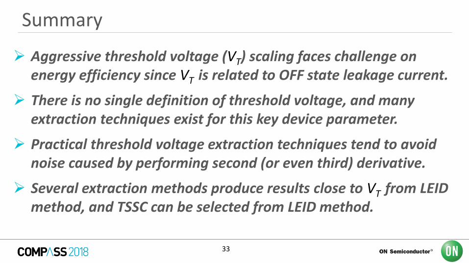
Summary
Aggressive threshold voltage (VT) scaling faces challenge on energy efficiency since VT is related to OFF state leakage current.
There is no single definition of threshold voltage, and many extraction techniques exist for this key device parameter.
Practical threshold voltage extraction techniques tend to avoid noise caused by performing second (or even third) derivative.
Several extraction methods produce results close to VT from LEID method, and TSSC can be selected from LEID method.
34
Test Insights from Lab to Fab
Technology-Specific Scaled Current (TSSC)
Id = Id0 x (W/L)
• Id0 can be selected from LEID method:
– Id0= (Id at VT) / (W/L)
• Id0 is Technology-Specific Scaled Current (TSSC) that applies to all geometries of the same device category.
• Id0 information can be used to monitor VT shift in reliability tests.
• Id0 information can be provided from lab to fab to save time on VT
measurements.
35
Acknowledgment
Chris Kendrick
Thomas Odenwalder
Michael Cook