Embed Size (px)
Citation preview

Journal of Microwaves, Optoelectronics and Electromagnetic Applications, Vol. 16, No. 3, September 2017 DOI: http://dx.doi.org/10.1590/2179-10742017v16i3897
Brazilian Microwave and Optoelectronics Society-SBMO received 20 Jan 2017; for review 26 Jan 2017; accepted 26 May 2017
Brazilian Society of Electromagnetism-SBMag © 2017SBMO/SBMag ISSN 2179-1074
675
Abstract— In this paper a wideband microstrip patch antenna
(MPA) using aperture coupling feeding technique with bandwidth
(BW) of 28% is designed at first. Afterwards for the pupose of
reducing the size of the radiating element, the composite right/left
hand (CRLH) concept is used by implementing an interdigital
capacitor (IDC) as series left hand component in the antenna. The
slot in the ground plane acts as a left hand parallel inductor.
Through this technique, three operation modes of CRLH antenna is
excited and by appropriate adjusting of the IDC parameters,
closing and mixing of resonant frequencies are achieved. Size
reduction in the order of 15.5% and 6.2% in the patch and slot
dimensions compared to the initial designed antenna is obtained
respectively. The equivalent circuit model of the final designed
antenna is presented and simulated. The final designed antenna is
fabricated and tested.
Index Terms— Compact, wideband, interdigital capacitor, equivalent circuit.
I. INTRODUCTION
The demands for compact, wideband and portable transceiver systems are the consequence of
increasing development of modern wireless communication. Since antenna is an important part in
transceiver systems with limited space in many applications, many efforts have been done to reduce
the size of antenna [1]. One of the limitations of MPA is its narrow BW which is in the order of a few
percent. Several techniques have been introduced for widening the BW of MPA including stacked
patch, proximity coupling, multimode techniques, implementing variations in the ground of the
antenna by defected ground structures (DGS) and changing shape of the patch [1], [2]. In this study,
aperture coupling feeding technique is used for BW increasing which was first introduced by Pozar in
1985 [3]. Several advantages of this method are: isolation of feed from radiating element, capability
of using different substrates for feed and patch with different thickness and permittivity which lead to
reduction of surface waves in the feed substrate and also antenna BW enhancement [3]. As it was
mentioned, besides being wideband, size reduction is an important subject in nowadays
communication systems. One way for size reduction is the utilization of metamaterials. Metamaterials
are artificially structured materials providing electromagnetic properties not encountered in the nature.
These materials are also called left handed materials (LHMs) due to the left handness of electric,
A Compact Wideband Patch Antenna
Loaded by Interdigital Capacitor with
Equivalent Circuit Model
Mojtaba Simruni, Shahrokh Jam
Department of Electrical and Electronic Engineering, Shiraz University of Technology, Shiraz, Iran,

Journal of Microwaves, Optoelectronics and Electromagnetic Applications, Vol. 16, No. 3, September 2017 DOI: http://dx.doi.org/10.1590/2179-10742017v16i3897
Brazilian Microwave and Optoelectronics Society-SBMO received 20 Jan 2017; for review 26 Jan 2017; accepted 26 May 2017
Brazilian Society of Electromagnetism-SBMag © 2017SBMO/SBMag ISSN 2179-1074
676
magnetic field and wave vector. Some of the other various specifications of LHMs are: reversal of
Doppler effect, inverse Snell’s law, changing of convergence and divergence effect in incidence of
wave to concave and convex lens [4], [5]. Also by using LHMs concept, size reduction in the
radiating element of the antenna is done [5]-[7]. Through using metamaterials, an antenna with
compact size, high efficiency and proper BW can be obtained. In this article, at first step, a wideband
aperture coupled MPA is designed. Then an IDC as a left hand series capacitor is implemented in the
patch [8]-[12]. The slot in the ground plane is a left hand parallel inductor which together with the
IDC offers a CRLH microstrip antenna. This is the main feature of this antenna. In the other works the
left hand inductor is imposed to the antenna by using microstrip line [13], cutting CSRR in the ground
[10], chip [14] or post-wall [11], [12], [16] but in this article the slot in the ground inherently acts as a
resonator and a left hand inductor simultaneously. In [10], through implementing an IDC in radiating
element and a complementary split ring resonator in the ground plane of the antenna, a CRLH antenna
has been proposed with BW of 6.8%. In [16], a CRLH antenna has been designed by using surface
integrated waveguide (SIW) as distributed left hand inductors and an IDC as series left hand
capacitor. The -10 dB impedance BW of this antenna is 1.52%. In [15], a two arm transmission line
metamaterial antenna with the BW of 3% has been proposed. Further size reduction of antenna has
been achieved in [15] in comparison with those in [10], [16]. In both of the antennas have been
investigated in [15] and [16], via is used in the structure. But a single layer vialess CRLH antenna,
using coplanar waveguide feeding technique has been offered in [17] with the BW of 6.8%. In our
work a three layer compact CRLH antenna with the BW of 28% is designed without via.
II. PROPOSED DESIGN
Among different feeding methods of MPAs, aperture coupling feeding technique is used in the
designing of initial antenna because of several advantages which was mentioned in section I.
Extended BW is the most important reason for choosing this kind of feeding method in this paper.
A. Wideband aperture coupled MPA
We first designed an aperture coupled MPA without IDC. According to Fig. 1(b) this antenna has
three layers. Feed layer with 0.762 , 2.5f rfh mm (Rogers ultralam 2000, loss tangent=0.0019),
patch layer1 with 8.6, 1p rph (air) and third layer above the patch which is similar to the feed layer.
Air gap is selected as the patch substrate to increase the BW of the antenna. The return loss and the
normalized radiation pattern of this antenna are shown in Fig. 1(c) and (d). The dimensions of the
antenna after optimization have been listed in table I. The BW of the antenna is 28% from 2.64 GHz
to 3.5 GHz (11S ≤ -10 dB). Electromagnetic simulations have been done by a full wave finite element
based simulator HFSS13 and circuit analyses have been performed by Microwave Office10 software.

Journal of Microwaves, Optoelectronics and Electromagnetic Applications, Vol. 16, No. 3, September 2017 DOI: http://dx.doi.org/10.1590/2179-10742017v16i3897
Brazilian Microwave and Optoelectronics Society-SBMO received 20 Jan 2017; for review 26 Jan 2017; accepted 26 May 2017
Brazilian Society of Electromagnetism-SBMag © 2017SBMO/SBMag ISSN 2179-1074
677
___ xz-plane
----- yz-plane
B. Inserting the IDC in the antenna
In the next stage for improving the features of the antenna, an IDC is implemented in the patch (Fig.
2). The effect of variations of capacitor parameters on antenna characteristics are shown in Fig. 3 and
4. The IDC which represents a left hand series capacitor is inserted in the center of upper semi part of
the patch. The dimensions of the capacitor in the first effort are as follow:
0 1 2 0 01 , 8 , 8.75 , 1 a a mm a mm b mm d mm (Fig. 3). 11S of this antenna is shown in Fig. 3(a). As it
can be seen, although there is some degradation in return loss of the original antenna after inserting
capacitor in it, but a new resonant frequency is added. Referring to Fig. 3 it should be noted that when
each of the IDC parameters is varied, the other parameters of the antenna and IDC remain constant.
Since the antenna acts as a one stage CRLH transmission line antenna and also according to the
equivalent circuit model of CRLH antenna (π-type), there are three resonances when M=1 [8].
, 0, 1n
p nM
(1)
(a) (b)
(c) (d)
Fig. 1. Initial designed antenna. (a) top view, (b) side view, (c) simulated11S ,(d) simulated normalized radiation pattern
(dB).
x y
x z

Journal of Microwaves, Optoelectronics and Electromagnetic Applications, Vol. 16, No. 3, September 2017 DOI: http://dx.doi.org/10.1590/2179-10742017v16i3897
Brazilian Microwave and Optoelectronics Society-SBMO received 20 Jan 2017; for review 26 Jan 2017; accepted 26 May 2017
Brazilian Society of Electromagnetism-SBMag © 2017SBMO/SBMag ISSN 2179-1074
678
Fig. 2. Aperture coupled MPA structure with IDC.
According to Fig. 3(a) by decreasing0a from 1mm to 0.25 mm the third resonance is shifted
downward whereas1a and
2a are constant. The third resonant frequency is equivalent to 1n . There
is no change in the first resonance by variation of 0a which belongs to 1n . When
0 0.25 a mm , the
second resonance (zeroth order resonance) is omitted. In Fig. 3(b), the effect of variation of 1a from
0.25 mm to 1mm is demonstrated whereas 0a and
2a are constant. As it can be seen, there is no
change in the first resonance; but by increasing1a , the second and the third resonances are shifted
upward simultaneously. The effects of variations of 0a and
1a are similar. In Fig. 3(c), the effect of
increasing 2a on
11S is shown. For 2 8 a mm the antenna has three resonances. In this step, by proper
tuning of IDC parameters, a wideband antenna can be achieved by closing and mixing these resonant
frequencies. Fig. 3(d) illustrates the effect of variation of 0d on the return loss of the antenna. By
decreasing 0d the third resonance is shifted downward.
The best result is achieved when0 0.5 d mm . The effect of shifting of the IDC toward the radiating
edge of the patch is presented in Fig. 4. The Second resonance of the antenna is weakened and the
third resonance is shifted downward but there is no change in the first resonance. Finally we choose
the best results from each part which lead to the BW enhancement.11S of the antenna after
implementing optimum IDC parameters is depicted in Fig. 5. It seems that the second and the third
resonances are mixed and the new BW is 830 MHz. Therefore, in the first step, a wideband aperture
coupled MPA without IDC is designed with BW=28% in S-band which the patch size is 35 35mm mm
and the slot size is 29 1.7mm mm . Then through an optimized IDC which is inserted in the patch, size
reduction is achieved. After several simulations, we reach an optimized patch which it’s 11S is
compared with the previous designs in Fig. 6.

Journal of Microwaves, Optoelectronics and Electromagnetic Applications, Vol. 16, No. 3, September 2017 DOI: http://dx.doi.org/10.1590/2179-10742017v16i3897
Brazilian Microwave and Optoelectronics Society-SBMO received 20 Jan 2017; for review 26 Jan 2017; accepted 26 May 2017
Brazilian Society of Electromagnetism-SBMag © 2017SBMO/SBMag ISSN 2179-1074
679
(a)
(b)
(c)
(d)
Fig. 3. Simulated return loss for different IDC parameters. (a) with0a variations, (b) with
1a variations, (c) with2a
variations, (d) with0d variations.
Journal of Microwaves, Optoelectronics and Electromagnetic Applications, Vol. 16, No. 3, September 2017 DOI: http://dx.doi.org/10.1590/2179-10742017v16i3897
Brazilian Microwave and Optoelectronics Society-SBMO received 20 Jan 2017; for review 26 Jan 2017; accepted 26 May 2017
Brazilian Society of Electromagnetism-SBMag © 2017SBMO/SBMag ISSN 2179-1074
680
Fig. 4. Simulated return loss for different
Fig. 5. Simulated return loss with optimum IDC parameters.
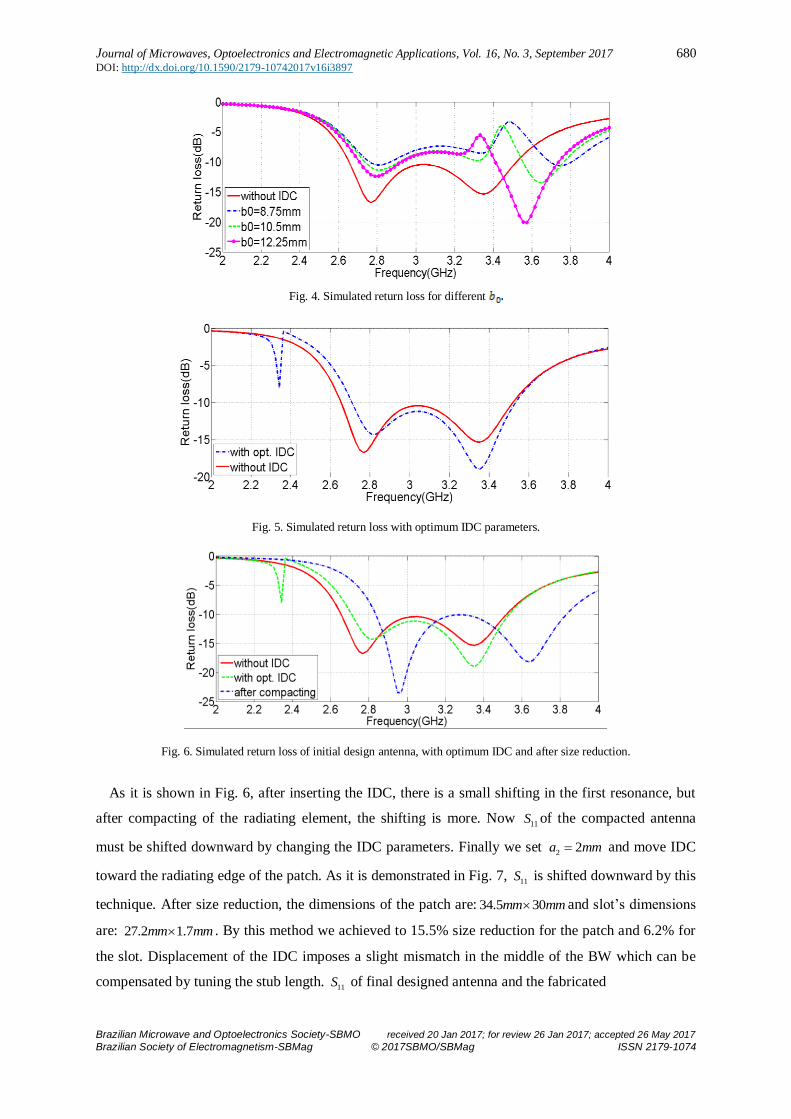
Fig. 6. Simulated return loss of initial design antenna, with optimum IDC and after size reduction.
As it is shown in Fig. 6, after inserting the IDC, there is a small shifting in the first resonance, but
after compacting of the radiating element, the shifting is more. Now 11S of the compacted antenna
must be shifted downward by changing the IDC parameters. Finally we set 2 2a mm and move IDC
toward the radiating edge of the patch. As it is demonstrated in Fig. 7, 11S is shifted downward by this
technique. After size reduction, the dimensions of the patch are: 34.5 30mm mm and slot’s dimensions
are: 27.2 1.7mm mm . By this method we achieved to 15.5% size reduction for the patch and 6.2% for
the slot. Displacement of the IDC imposes a slight mismatch in the middle of the BW which can be
compensated by tuning the stub length. 11S of final designed antenna and the fabricated

Journal of Microwaves, Optoelectronics and Electromagnetic Applications, Vol. 16, No. 3, September 2017 DOI: http://dx.doi.org/10.1590/2179-10742017v16i3897
Brazilian Microwave and Optoelectronics Society-SBMO received 20 Jan 2017; for review 26 Jan 2017; accepted 26 May 2017
Brazilian Society of Electromagnetism-SBMag © 2017SBMO/SBMag ISSN 2179-1074
681
Fig. 7. Simulated return loss for different displacement of IDC
prototype is depicted in Fig. 8. According to Fig. 10(a), the gain of the antenna is varied from 8.73 dB
to 10 dB in the BW. The normalized radiation pattern in the xz-plane and yz-plane is illustrated in
Fig. 10(b). The dimensions of the final designed antenna have been listed in table I.
III. EQUIVALENT CIRCUIT MODEL
In this section, an equivalent circuit model of final designed antenna (compacted antenna) with the
IDC is presented. According to Fig. 8, the model is consisted of input transmission line (TL), first
coupling transformer, parallel LC tank which is equivalent to the slot, second coupling transformer
and patch impedance [18]. The patch impedance is comprised from lower and upper parts. The upper
part of the patch is divided into two TLs which the IDC is inserted between them. It is necessary that:
4 5 0/ 2pL L L a . Values of 4 1 1 2, , , ,C L C N N can be calculated by the formulation offered in [19]-
[20]. The values of the lumped elements and the other parameters in the equivalent circuit model are:
1 2 3 4 5 1 2 1 2 3 4, , , 16 , 1 , 347 , 0.9 , 0.384 , 3.42 ,2
p
f stub
LL L L L L L mm L mm R R C pF C C pF C F
1 20964, 0.385, 1.977N N LL nH
It should be mentioned that through using formulas, initial values of lumped elements are
calculated then for better compatibility of circuit model simulation results with full wave
electromagnetic counterpart, tuning of elements values is necessary. The simulation result of circuit
model is depicted in Fig. 9.

Journal of Microwaves, Optoelectronics and Electromagnetic Applications, Vol. 16, No. 3, September 2017 DOI: http://dx.doi.org/10.1590/2179-10742017v16i3897
Brazilian Microwave and Optoelectronics Society-SBMO received 20 Jan 2017; for review 26 Jan 2017; accepted 26 May 2017
Brazilian Society of Electromagnetism-SBMag © 2017SBMO/SBMag ISSN 2179-1074
682
Fig. 8. Equivalent circuit model of the final designed antenna.
IV. MEASUREMENT RESULTS
Final designed antenna is fabricated on ultaralam2000 printed circuit board (PCB). The patch and
the feed line are implemented on two separate PCBs. The air gap between two layers is implemented
by a frame of Teflon with loss tangent of 0.001. Fig. 11 shows the fabricated antenna. The return loss
of the antenna is measured by 8510C network analyzer. There is a good agreement between
measurement and simulation result of final designed antenna.
Table I. Dimensions of the initial and final designed antenna
parameter pL pW
sL sW fL
Value(mm)
Initial
design 35 35 29 1.7 50
Final
design 34.5 30 27.2 1.7 50
parameter fW
stubL 0a
1a 2a
Value(mm)
Initial
design 2.15 4.7 - - -
Final
design 2.15 4.2 0.25 0.25 2
parameter 0d
0b ph fh 1L 1W
Value(mm)
Initial
design - - 8.6 0.762 60 60
Final
design 0.5 16 8.6 0.762 60 60

Journal of Microwaves, Optoelectronics and Electromagnetic Applications, Vol. 16, No. 3, September 2017 DOI: http://dx.doi.org/10.1590/2179-10742017v16i3897
Brazilian Microwave and Optoelectronics Society-SBMO received 20 Jan 2017; for review 26 Jan 2017; accepted 26 May 2017
Brazilian Society of Electromagnetism-SBMag © 2017SBMO/SBMag ISSN 2179-1074
683
____ xz-plane
------ yz-plane
2 2.2 2.4 2.6 2.8 3 3.2 3.4 3.6 3.8 4-35
-30
-25
-20
-15
-10
-5
0
Frequency(GHz)
Retu
rn loss (
dB
)
without IDC
with opt. IDC
after compacting
after shifting of s11
measurement
circuit model
Fig. 9. 11S of final designed antenna and fabricated prototype.
(a)
(b) Fig.10. Simulated characteristics of final designed antenna. (a) Gain (dBi), (b) Normalized radiation pattern (dB)

Journal of Microwaves, Optoelectronics and Electromagnetic Applications, Vol. 16, No. 3, September 2017 DOI: http://dx.doi.org/10.1590/2179-10742017v16i3897
Brazilian Microwave and Optoelectronics Society-SBMO received 20 Jan 2017; for review 26 Jan 2017; accepted 26 May 2017
Brazilian Society of Electromagnetism-SBMag © 2017SBMO/SBMag ISSN 2179-1074
684
(a) (b)
Fig. 11. Photograph of fabricated antenna (a) patch and feed boards, (b) assembled antenna.
V. CONCLUSION
A wideband aperture coupled MPA with the BW of 28% has been designed at first. Then through
inserting an IDC and by optimum tuning of its physical dimensions and location, size reduction of the
patch and the slot in the order of 15.5% and 6.2% is achieved respectively. Effects of variation of IDC
parameters on the antenna return loss are studied in detail. The IDC and the slot in the ground plane
offered a CRLH antenna which allows more size reduction whereas the antenna remains wideband.
To obtain better insight into performance of the antenna, a circuit model is developed. The prototype
of the antenna has been fabricated and there is a good agreement between circuit and full wave
simulation with measurement result.
REFERENCES
[1] N. Nasimuddin, Microstrip Antennas, Intech Publisher, 2011. [2] H. Malekpoor, and Sh. Jam, “Design of a multi-band asymmetric patch antenna for wireless applications,” Microwave
Opt. Tech. Lett., vol. 55, pp. 730-734, 2013.
[3] D. M. Pozar, “A review of aperture coupled microstrip antennas: history, operation, development, and applications, Internet Archive of Univ. Massachusetts at Amherst,” archived at http:/www.ecs.umass/ece/pozar/aperture.pdf, May 1996.
[4] C. Caloz, and T. Itoh, Electromagnetic metamaterials: transmission line theory and microwave applications, New York, Wiley-IEEE Press, 2005.
[5] N. Engheta, and R. N. Ziolkowski, Electromagnetic metamaterials:physics and engineering explorations, New York, Wiley-IEEE Press, 2006.
[6] A. Jafargholi, and M.H. Mazaheri, “Broadband microstrip antenna using epsilon near zero metamaterials,” IET
Microwaves Antennas Propag, vol. 9, no. 2, pp. 1612-1617, 2015. [7] W.Q. Cao, “Compact dual band dual mode circular patch antenna with broadband unidirectional linearly polarized and
omnidirectional circularly polarized characteristics,” IET Microwaves Antennas Propag.,vol. 10, no. 2, pp. 223-229, 2016.
[8] Y. Dong, and T. Itoh, “Metamaterial-based antenna,” in Proc IEEE, vol. 100, no. 7, pp. 2271-2285, 2012. [9] K. Wong, Compact and broadband microstrip antenna, John Wiley & Sons Inc, 2002. [10] G. Ha, K. Kwon, Y. Lee, and J. choi, “Hybrid mode wideband patch antenna loaded with a planar metamaterial unit
cell,” IEEE Trans. Antennas propagat, vol. 60, no. 2, pp. 1143-1147, 2012.
[11] A. P. Saghati, and K. Entesari, “A miniaturized switchable SIW-CBS antenna using positive and negative order resonances,” in Proc IEEE Int. symp. Antennas Propag., pp. 566-567, 2013.

Journal of Microwaves, Optoelectronics and Electromagnetic Applications, Vol. 16, No. 3, September 2017 DOI: http://dx.doi.org/10.1590/2179-10742017v16i3897
Brazilian Microwave and Optoelectronics Society-SBMO received 20 Jan 2017; for review 26 Jan 2017; accepted 26 May 2017
Brazilian Society of Electromagnetism-SBMag © 2017SBMO/SBMag ISSN 2179-1074
685
[12] S. Sam, and S. Lim, “Compact frequency-reconfigurable half-mode substrate-integrated waveguide antenna,” IEEE Antennas Wireless Propag. Lett., vol. 12, pp. 951-954, 2013.
[13] A. Sanada, K. Murakami, I. Awai, H. Kubo, C. Caloz, and T. Itoh, “A planar zeroth-order resonator antenna using a left-handed transmission line,” in Proc 34th Eur. Microw. Conf., Amsterdam, The Netherlands, pp. 1341-1344, 2004.
[14] J. Choi, and S. Lim, “Frequency and radiation pattern reconfigurable small metamaterial antenna using its extraordinary
zeroth-order resonance,” J. Electromagn. Waves Appl, vol.24, pp.2119-2127, 2010. [15] J. Zhu, and G. V. Eleftheriades, “A compact transmission-line metamaterial antenna with extended bandwidth,” IEEE
Antennas Wireless Propag. Lett., vol. 8, pp. 295-298, 2009. [16] Y. Dong, and T. Itoh, “Miniaturized substrate integrated waveguide slot antennas based on negative order resonance,”
IEEE Trans. Antennas propag., vol. 58, no. 12, pp. 3856-3864, 2010. [17] T. Jang, J. Choi, and S. Lim, “Compact coplanar waveguide (CPW)-fed zeroth order resonant antennas with extended
bandwidth and high efficiency on vialess single layer,” IEEE Trans. Antennas propag., vol. 54, no. 2, pp.363-372, 2011.
[18] R. Garg, P. Bhartia, I. Bahl, and A. Ittipiboon, Microstrip antenna design handbook, Artech House Inc, 2001. [19] C. A. Balanis, Antenna theory analysis and design, john wily & sons Inc, 2005. [20] K. C. Gupta, R. Garg, I. Bahl, and P. Bhartia, Microstrip lines and slotlines, Artech house, London, 1996.


![Miniaturized Triple Wideband CPW-Fed Patch Antenna With a ... · Double L-slot microstrip patch antenna array for WiMAX and WLAN applications is proposed in [20]. A coplanar waveguide](https://img.pdfslide.us/doc/110x75/5f14d7603b24ad1cb956d521/miniaturized-triple-wideband-cpw-fed-patch-antenna-with-a-double-l-slot-microstrip.jpg)